Embed Size (px)
Citation preview

ABSTRACTEnergy & Eco-Sustainability using Pressure-less Silver Sintering for RF Power Electronics
A virtually void free die attach was successfully achieved using a fixed but critical volume of Ag sinter paste by a pro-cess of pressure-less sintering on a multi-axis cartesian style bonder, retrofitted with a high-speed jetting dispenser. While this process potentially offered an ideal combination of cost-effectiveness, control and speed, it required the development of additional software protocols to secure the level of performance demanded of the dispenser to meet exacting technical requirements. This proprietary adaption we term “Fixed BLT” software, and over five test pieces we were consistently able to deliver a fixed height bond-line of circa 70% of bond height, translating as 50μm before sinter and 30μm after. In each case the result was a virtually void free bond secured in a timely, repeatable, commer-cially effective manner. The absence of voids was verified through industry standard non-destructive analysis utilizing C-mode scanning acoustic microscope (CSAM).
1. Case Study
Silver sintering technology has been around since the 1980s, but the process has faced numerous problems. The lim-its of traditional sintering, rapidly growing market demand, 5G, evolving technologies, issues of energy and eco-sus-tainability, together with lead-free requirements, have, however, led many to revisit these challenges. Since 2016 especially, these efforts have gained more traction, moving from research to commercialization driven by innova-tion in nano-particle material sciences, greater emphasis on energy effectiveness and eco-sustainability, and the widespread adoption of lead-free legislation across the globe. This paper will review the work that Palomar has undertaken to develop sustainable packaging and assembly die attach, using pressure-less silver sintering for high temperature (>300 ͦC) power electronics.
As a bonding technology, silver sintering promises a void-free, strong bond, with superior thermal and electrical con-ductivity. It has the ability to decrease the junction temperature (Tj) of a device up to 100 ͦC. In the process, when the silver material is heated under optimal circumstances (pressure, temperature and time) its form will change from powder to a solid structure. Compared to traditional solder material, the action of sintering results in a more reliable bond, significantly increasing performance and lifetime, while being more energy efficient and placing less stress on the package.
2. Introduction and Background
To better convey the relevance of our case study, we must first examine the solder alloys that are used in conventional eutectic die attach. In terms of RF power electronics, and as shown in Table 1, these fall into four category types.
Energy and Eco-Sustainability using Pressure-less Silver Sintering for RF Power Electronics
Authors: Evan A. Hueners, Richard D. Hueners,Anthony D. F. O’Sullivan, M. Redzuan Zin.
Making the connected world possible™

Table 1. - Solder Alloys for RF Power Electronics.
Historically, eutectic die attach using solder alloys has been preferred because it copes well with high temperatures and is widely proven for performance and reliability. However, it now faces a number of perhaps insurmountable challenges: materials such as AuSn though very reliable, are notoriously slow to process and expensive; furthermore, the bonding processes they utilize require increasingly unacceptable energy costs on the one hand, and place un-desirable packaging level stress, on the other. Though Pb-Sn offers reliability, performance, and lower cost, global environmental requirements for lead free manufacturing now preclude this option.
3. Alternatives to Traditional Solder
Die attach materials need to withstand operating temperatures of up to 300 ͦC for SiC based power modules; in comparison, Si-based devices have a maximum junction temperature of 175°C. As Ag sintered bond processes can be performed at lower temperatures (below the melting point of the resulting bond), they endure less residual stress than their eutectic bonded counterparts. Ag sintering has the additional benefit of being lead-free.
Extensive research demonstrates that Ag sintering works well with wide-band gap materials such as GaN and SiC due to its temperature capability (tested up to 500 ͦC). When combining GaN die on SiC substrates and using Ag sintering to make the bond, the lower temperatures will result in less residual stress while retaining high operating tempera-tures. We now consider in further detail the choice of alloy, the mechanics/advantages of a pressure-less application, and their comparison to more traditional alternatives:
3.1. Choice Alloy: Ag
Gold has been the preferred alloy in high temperature power applications due to its excellent material properties. However, with gold at a five year high and anticipated to move towards a record, and with increasing demand for power electronics, a more scalable and long-term solution is needed. Against this backdrop, silver presents an excel-lent alloy and a highly viable alternative, offering:
1. Excellent thermal and electrical performance. 2. Lower material cost. 3. Low temperature sintering.
Table 2. - Material Comparison
Type Characteristics Consideration ThermalConductivity
SACs Sn, Ag, Cu with a melting temp of 200°C+, lead-freeSAC solders use more than lead-tin solders, prone to voiding because of the transition from solid to liquid.
SAC 305: 58.7 W/mK
HMP(High melting point)
280°C melting pointHigh lead content, prone to voiding because of
transition from solid to liquid.PbIn: 17 W/mK
Gold-based AuSn, AuGe, AuSi up to 362°CCostly due to high gold content, prone to voiding
because of transition from solid to liquid.AuSn: 57 W/mK
Lead-free solders Ag, Au, Bi, Cu, Ga, Ge, In, Mg, Sb, Sn, Zn.High temperature, costly, prone to voiding because
of transition from solid to liquid.Cu: 385 W/mK
Material/Specifications AuSn Ag Sinter
Thermal Conductivity (W/mK) 58.7 50-300
Electrical Resistivity (micro-ohms cm) 20.7 20
Cost (USD/oz) Au: 1507 Ag: 18.19
Melting Point (°C) 280 °C 961 °C
Image Source: KYOCERA

3.2. Pressure-less Ag Sintering
Significant inherent technical advantages include:
1. Silver can be sintered in the presence of air.
2. Silver can be dispensed using the same set of tools and with a similar procedure as solder paste; a straight-forward “drop-in” solution.
3. Pressure-less sintering does not require special tooling to avoid damaging the die, as needed in alternative pressured (240 ͦC temp + 100 MPu) uses.
4. Ag sinter paste can be deployed with nano-particles that increase the surface area coverage; smaller particles have more free energy and need less external energy to fuse.
5. Pressure-less sintering allows for the coverage of larger surface area dies. Moreover, silver paste compounds optimize results with low porosity. This is a relatively new and technically significant innovation.
6. Ag sinter paste can match AuSi and AuSn in terms of thermal conductivity.
3.3. Comparing Silver to Lead
Establishing that sintered Ag is a technically effective alternative to Pb, research shows that Ag sintering material capability is beyond that of high-Pb in respect to:
1. Processing temperature similar to, or even lower than, current high-lead solders.
2. Higher service temperature capabilities due to its high melting point 961 ͦC (We estimated the silver joint service temperature as 470–530 ͦC according to the shear strength vs. temperature relationship).
3. Higher value of thermal conductivity as compared to that of solder.
4. Superior mechanical and electrical properties versus other lead-free alternatives.
5. Successful sintering using pressures of 20 to 40 MPa, lower pressures and even zero pressure.
6. Compatibility with existing manufacturing processes (“drop-in” solution).
4. Pressure-less Silver Sintering
We now explicate the work undertaken to create a virtually void-free die attach with a fixed volume of Ag sinter paste. The process utilized pressure-less Ag sintering on a multi-ax-is cartesian robot-style die bonder, retrofitted with a high speed jetting dispenser. We emphasize “pressure-less” so as to not be confused with conventional Ag sintering, or rather, pressured Ag sintering, where the die attach is performed in a reflow oven or in an environment where pressure can be applied. Previously, time-pressure dispense was the tool of choice for die bonder driven Ag sinter paste dispense, be-cause of its low cost, widespread availability, ease of use, and good results. However, with increased demands from RF power electronics manufacturers for better voiding con-trol and higher yielded throughput, a different method of dispense had to be developed. Jet dispense technology presented the ideal combination of control and speed. Not-withstanding, jet dispense proved insufficient on its own to achieve a fixed height bond line and low voiding results; only when combined with our proprietary “Fixed BLT” software were we able to deliver a fixed height bond line of 50μm before sinter and 30μm after sinter with excellent planarity, a virtually void-free bond, and in a time-effective fashion. See Table 3 for Ag sinter material specifications used in this case study:
Paste Property
Ag Concentration:Viscosity:Bonding Area:
90-93%20-60 Pa-s<5x5 mm2
Applied Condition
Atmosphere:Sintering Temperature:Recommended BLT:
Air.200°C-230°C10-30 μm
Process Margin
Pot Life:Printing and Mounting:Mounting and Sintering:
24 hours1 hour4.5 hours
Sintering Properties
Specific Resistance:Shear Strength:
2-2 μΩ-cm.>30 MPa.
Reliability TCT Condition: 1000 cycles -55° - 150°C
StorageTemperature:Period:
-40°C to 10°C6 Months
Curing
Ramp-up Rate:Peak Temperature:Time:Atmosphere:
3-5°C/Min.210°C-230°C60 Min.Air
Table 3. - Ag Sinter Material Specifications

The selection of Ag sinter material was chosen partly because it is readily available and partly because it reflects appli-cation demands. Bond line height or bond line thickness is referred to frequently in this paper. While bond line height requirements will differ across the industry, we tried to model our experiment around those most common, possessing optimum functionality, most likely to be used in these packaging applications. To measure bond line void, we used a C-mode scanning acoustic microscope (CSAM). CSAM scans for voids across multiple depths of the bond line and allows for a statistically relevant set of images to inspect. It is also an accepted industry practice. The die bonders, metrology and test tools used in this case study are exactly those used in, for example, eutectic die attach for RF power electronics, epoxy attach for CoB (chip on board), and CoC (chip on carrier) sub-assemblies in opto-electronic applications.
It was particularly vital to demonstrate that this capability can be “dropped-in” to existing tool sets and deliver the required pressure-less Ag sintering results demanded by RF power electronics. It is important to note that we did not perform electrical testing of the device or device performance cycling. Instead, we assumed that void-free bond lines would result in lower operating temperatures and better device longevity; the fixed height BLT would result in the cor-rect amount of material needed for optimal device performance. Our assumption is based on the preponderance of data and analysis in the public domain. While studying the entire supply chain to design, fabricate, and build a high quality RF device for market delivery goes well beyond the scope of this paper. Nevertheless, we intended to contribute a small butessential knowledge of the RF device’s journey to the end customer: the process of attaching the GaN die to a substrate in a manner that is cost-effective, eco-friendly, sustainable, and high performing.
4.1 Methodology and Rationale
To ensure this application reflected an industrially authentic, repeatable process, the work was performed at Palo-mar’s Innovation Center in Singapore, using a Palomar 3880 Die Bonder and a “drop-in” jet dispenser in the Class 100k clean room with locally sourced materials. (See Figure 1).
Figure 1 - Palomar’s Singapore Innovation Center — Case Study Process
Figure 1a: Palomar 3880 work envelop with GaN on the waffle pack/Gel-Pak. A 2x2 inch coupon acted as substrate; the Musashi Aerojet dispensed the Ag sinter then attached the die. The dual wafer presentation (not shown) approxi-mates commercial production.
Figure 1b: The bonder process view camera shows a Vespel pick-up tool designed for high aspect ratio die. The bonder hovered over the GaN die on the waffle pack/Gel-Pak and with vacuum suction on the tool tip, picked up the die and placed it in the targeted location.
4.2. Defining the Case Study Parameters
A. The defining parameters for the case study: 1. Surface Height Measurement Repeatability.
2. Substrate Topography (flatness and roughness).
3. Line Consistency.
B. The defining metrics for the case study: 1. Wet Bond Line Thickness (BLT) is 42.5 μm ±7.5 μm. (Before sintering)
2. Dry Bond Line Thickness (BLT) is 27.5 μm ±7.5 μm. (After sintering)
3. Fillet coverage 100% of die perimeter.
4. Fillet height aiming for 70% of, but not exceeding, die height.
5. Zero void tolerance.
5. Dispensing Technologies
5.1. Background
A fixed bond line thickness is both important and necessary. Of itself it does not secure a void-free attach, nor does it contribute in a meaningful way to mechanical stability. The real issue lies in the consistency of the material com-position; a designated number of Ag particles would achieve the required performance. Hence the need for a fixed amount of material (bond line) under the die.
To ensure the material volume was consistent and the process was repeatable, it was critical to ensure the devel-opment of a controlled, highly accurate, consistent, and process-repeatable bond line thickness (BLT) or “Fixed Height BLT”; a uniform adhesive layer delivered across the bonded area. “critical” because even small inconsisten-cies produced peel stresses resulting in reduced adhesion strengths. A line that is is too thick ( >50 μm) will result in increased resistance negatively impacting electrical performance. Overly thin bond lines (<30 μm), on the other hand, tend to cause voids, adhesive starvation, and de-bonding also undermining long-term device performance. We will expand on the nature and importance of our proprietary Fixed Height BLT technology in sections 7.1, 8.7 and 9.3 below.
While optimum bond line thickness depends on the type of adhesive, the samples used in our case study found that 50 μm before sintering—and 30 μm before sintering—secured the best results; these numbers were also rec-ommended by the supplier of the Ag sinter paste used. Part of our process was to match the quantity of available Ag material to the gap between the surfaces and their bonding conditions (heat and pressure). A slight overfill was desired to ensure that the gap was totally populated. Earlier trials also found that adhesive would squeeze out of a local area if there was a high spot in one of the adherents.
5.2. Metrology
The next set of critical issues were compensation and control, which in turn required effective metrology. The mea-suring methods adopted/results achieved are shown in Fig. 2 below. Gauging bond line thickness can be variously achieved, for example, by measuring die height after bonding/after sintering (using a digital microscope) and sub-tracting the thickness of the die (measured before bonding/presintering). Height measurement can also be secured with either the focus-variation or 3D scanning. Regardless of the choice here, the bond line thickness should be measured at different positions to evaluate uniformity. Figure 2c records BLT by measuring the height at the four corners (upper left and right, lower left and right) of the die.

Figure 3 - Flatness and Roughness of Coupon
A consistently flat surface that includes sufficient roughness is vital for an accurate, correct, and repeatable BLT. While these two objectives may sound contradictory, typical RF substrate surfaces are designed in such a manner to ensure material can be placed consistently, tacked, and fused to the board. Any variable in these factors will not just affect mea-surement, but the measured height upon which it is pred-icated, and finally the BLT height itself. Collectively these determine the accuracy of the post reference height mea-surement. In our study we used a flat gold-plated coupon, a common test vehicle that was both sufficient to our needs and effectively mimicked a typical RF substrate.
Our method for verification (see Figure 3) was to use confo-cal microscopy to provide a visual and qualitative measure-ment of the surface using confocal microscopy.
5.4. Verifying Touch Contact Repeatability
Measured touch height was used to determine the height of the bonding surface prior to the post reference height check. The intent was to calibrate the bonder with a physical test; this was followed by software simulations to better understand and more successfully ensure the repeatability of the die bonder’s subsequent packaging process. (See Figure 4)
Timer and axis positions logged to record the position of Z-axis during the touch test over 100 cycles. Several test matrices were then drawn from the results and subsequently used to establish the accurate parameters necessary for repeatability. These became the basis for the subsequent case work undertaken.
5.3. Substrate Flatness and Roughness
Figure 2 - BLT Results
Figure 2a. 3D Optical/Laser microscope.
Figure 2b. Cross sectionmeasurement.
Figure 2c. BLT is measured by finding respective height at the four corners of the die.

6. Dispensing Ag Sinter Paste
Figure 4 - Verifying Measured Height Repeatability
Height tests were undertaken over 100 cycles. These results verified that measured height at a range of 3.175μm was well within our required specifications.
Our initial fixed height bond line utilized a time-pressure dispense pump. Only when the limitations of this method become apparent did we seek an alternative. This lesson was an invaluable part of the study’s background allowing us to review/test alternative contact dispensing technologies. These are listed below together with what we judge their concomitant advantages and disadvantages:
6.1. Time and Pressure Dispensing
This process uses a syringe and a pneumatic valve. This process utilizes controlled and timed air pressure that forces fluid out of the syringe via a dispensing needle and onto the work surface. Pressure is removed to stop material flow. Fluid flow is proportional to the amount and duration of the applied pressure.
Advantages: low cost, easy to use, widely available.
Disadvantages: Dot sizes decrease over the process as the plunger does not advance equidistantly with each air shot. While this can be adjusted, operator dependence increases the likelihood of human error. The user must main-tain a consonant dispense height relative to surface in order to produce consistent dots. In the case of Ag sinter dispense, maintaining the right viscosity is also essential to the process; as temperature inside the pump cannot be controlled, the standard time-pressure pump has no means by which to ensure this optimal viscosity, making it un-satisfactory for repeatability and efficiency. The result is limited usability. Finally, time-pressure is also notoriously slow in comparison to jetting.
6.2. Auger Pump
Based on an Archimedes’ screw within a cartridge to eject material. The process uses a motor to drive to engage/disengage screw motor/fine tuning ejection. Air pressure forces material into the pump. Higher-end products can be programmed to dispense a directed, specific, and directed amount of liquid.
Advantages: Programmable dispense, control.
Disadvantages: Slow speed, expensive relative to value. Like time-pressure, the auger pump is susceptible to part height variations. The user must maintain a consistent dispense height relative to surface in order to produce consis-tent dots. Furthermore, the standard auger pump has no way to keep the Ag sinter paste viscosity in its optimal state.
Touch Test (μm)

6.3. Positive Displacement Pump
Piston forces material through a needle, in turn controlled by a DC servo motor/precision encoder. Deposition time is fast but in other critical respects is dependent on piston size and length inside the chamber for consistency.
Advantages: Fast, precise.
Disadvantages: Susceptibility to fluctuations in viscosity. Pressure must be constantly and precisely adjusted. With Ag sinter paste, maintaining the correct viscosity is essential to a good process, hence a pump of this type is not recommended.
7. Jet Dispensing
With traditional dispense contact methods as we have considered them, a needle touches down, moves up to dis-pense height, then physically applies the fluid; with non-contact dispensing, a jet hovers over the location and shoots fluid at the work surface without touching it. This is what we mean by “non-contact” dispensing. Thus, jet dispensing is also referred to as non-contact dispensing—it delivering as it does, adhesive dots at high speeds from a height between 1mm and 3mm above the surface.
This non-contact proved vital because it inherently minimized adhesive tailing (using positive shutoff), allowed for tighter pitch, deeper access, and reduced chances of damaging the die. None of the alternative pumps could deliver this demanding level of performance. Moreover, the Z-axis motion is eliminated during dispensing, yielding a factor 10 increase in process speed (1000 dots/min). The mechanics of the jet dispenser made it possible to program differ-ent sized dots and to jet multiple shots in the same location. With a temperature controlling system integrated into the jet pump assembly, optimal viscosity was maintained at all times. With bond line control and voiding so essential in RF power electronic devices, the jet dispenser was proven to deliver exceptional results: tighter process control, significantly better repeatability, and dot consistency.
7.1. Combining Fixed Height Bond Line and Jetting Technologies
Having established the advantages of jet dispensing, and having outlined our success in securing speed and repeat-ability via our proprietary process, we now need to further expand on the unique and complementary capabilities that mark Palomar’s Fixed Height BLT itself.
As we have already alluded, the technology is based on combining software and process, making it tangibly invisible to the user. It yielded precise control in both dispensing and bonding height. The fundamentals of the process un-dertaken are outlined in Figure 6.
Figure 5. Musashi’sAeroJET Dispense Pump

Figure 6 - Fixed Height Bond Line Process Technology
Figure 6a. Dedicated tool was assigned to measure the substrate surface height.
Figure 6c. The Jet dispensed the Ag Sintering paste at a height calculated from the reference height.
Figure 6b. The measurement tool touched the bondingsurface to record the reference height.
Figure 6d. After vacuum pickup the die was placed/bonded on the dispensed Ag sintering paste.
Figure 6e. The die was bonded on the dispensed Ag sintering paste set to a specific height (in this case 50 μm) calculated from the reference height.

8. Technical Overview
8.1. Defining metrics
1. Wet Bond Line Thickness (BLT) at 42.5 μm ±7.5μm.
2. Dry Bond Line Thickness (BLT) at 27.5 μm ±7.5μm.
3. Fillet coverage 100% of die perimeter.
4. Fillet height at least 70% of the die height but not exceeding die height.
5. Zero void tolerance or Voiding 100%.
8.2. Application materials
1. GaN die size 5232.4 μm x 876.3 μm x 108.4263 μm.
2. 2x2 inch gold coupon.
3. Ag sinter paste (see Table 2 for specification).
4. Custom vespel pick and place tool, specified for GaN die.
8.3. Tools to perform application
1. Palomar Model 3880 Die Bonder.
2. VisionPilot® with Radar Referencing® option.
3. Waffle pack/Gel-Pak Presentation Stage option.
4. Keyence VHX-6000 Digital Microscope.
5. Musashi Aero-JET Dispenser.
6. Sonix HS-1000 C-Mode Scanning Acoustic Microscope (C-SAM).
8.4. Material Loading and Presentation
The GaN die were manually loaded on the waffle pack/Gel-Pak presentation stage. In authentic production scenarios these GaN dies will come either pre-placed on waffle pack, Gel-Pak, or on wafers. In both cases the bonder’s func-tions are the same: dispense Ag sinter, pick and place GaN die on the substrate and bond. The key difference in wafer presentation is the additional action of punching-up the GaN die from the wafer before picking or simultaneously with picking. Either method is efficient. The pickup tool was cleaned with isopropyl alcohol (IPA) and visually inspect-ed above the camera prior to bonding (See Figure 1 for bonder set-up).
A bespoke program was developed using our standard client software to dispense the Ag Sintering material and pick and place the GaN die on the coupon.
8.5. Process Considerations and Steps
Our test process utilized five GaN dies to establish the repeatability of the Ag sintering material viscosity change over time (with an estimated 90 minutes interval time between each die). Standard boundaries of bond force, axis speed, etc. were applied to picking the GaN die and placing it onto the coupon while adhering to the necessary height pa-rameters (the BLT35-50 μm range).
8.6. Sequence of Operation
1. Gold coupon was manually loaded onto the presentation stage and vacuum clamped.
2. Touch tool height measurement.
3. Ag sinter dispensed on bonding location at a 127 μm height.
4. Customized pickup tool moved GaN die from the presentation stage to sintered location/substrate.

5. GaN die placed onto sintered material using Fixed Height BLT technology.
6. Coupon manually removed and wet (before sinter) BLT measurement secured.
7. Curing profile ramped from 25°C→ 210°C (3°C/min ) and soaked in 210°C for 60 minutes.
8. Measured for dry (after sinter) BLT.
8.7. Fixed Height BLT Technology
In regards to Fixed Height BLT engagement the first step was to input the required height specification of 50 μm (about 2 mils) into the 3880 Die Bonder interface. As previously noted, the proprietary software had been designed to make this programing function as fast and straightforward as it was effective. Subsequently the bonding surface touch tool recorded our “reference height” (substrate height). With our Fixed BLT 50um parameter already in place, and using the reference height now established, the dispenser jetted the Ag sinter paste from a height approximately 2.5 times greater than the height of the desired bond line. As shown in Fig. 8 below the die was then placed using fixed height bond line technology—this successfully covered the bottom surface area while simultaneously maintain-ing the 50um BLT height.
9. Findings and Results
9.1. Dispense Line Consistency
A total of 15 lines were dispensed on the coupon/substrate, with measurement following immediately upon com-pletion. The results demonstrated a width, length, and height consistency within the 15 μm tolerance range and well within our specification of 25.4 μm. Figure 7 shows the width, length, and height measurement result of the Ag sintering lines jet dispense using Musashi AeroJET on the coupon.
Figure 7 - Dispense Line Consistency (μm)
Figure 8 - Epoxy Coverage
Figure 8a. 100% coverage on die perimeter.
Figure 8b. Epoxy >70% not exceeding the die height.
Figure 8c. Epoxy >70% notexceeding the die height.
9.2. Epoxy Coverage
Referring to defining metric of achieving fillet coverage 100% of die perimeter, we achieved 100% epoxy coverage to 70% of the die height on each of the five test pieces. The GaN die test pieces and results are illustrated in Figure 8. The token presented from top and corner views; the remaining four dies showed at least equal, if not slightly better results.
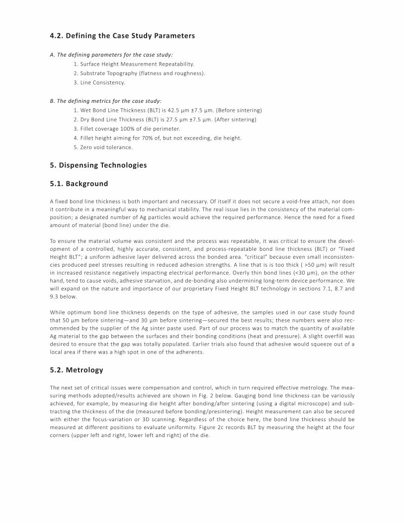
9.3. Bond Line Thickness (BLT)
Using the focal 3D function on the confocal microscope, we referenced/measured the corner top surface of the die to establish bonding height after cure. The bonder measured the substrate surface height by touching the center where the die placement later occurred; the bond line thickness was accounted as one of our defining parameters. From this juncture, there were no further touches to the substrate surface. As previously mentioned, the die height was defined as die thickness + bond line thickness. The die thickness (108.4263 μm) was subtracted from the die height to get the effective BLT. As our results show (Figure 9 below) we achieved our stated specification of a wet Bond Line Thickness (BLT) of 42.5 μm ±7.5 μm and a dry Bond Line Thickness (BLT) of 27.5 μm ±7.5 μm. Measurements are shown for upper left, upper right, lower right and lower left, of the bonded GaN die coupon.
Figure 9 - BLT Measurement
Each die was bonded with estimated 90 minutes interval time including the curing and measurement process. The Wet and Dry BLT (μm) results show a highly consistent range, improving after sinter (dry). The after sinter shrinking is caused by the organic matter and volatiles burning off.
Wet BLT (μm) Dry BLT (μm)

9.4. Scanning for Voids
Voiding was measured using a Sonix HS-1000 C-Mode Scanning Acoustic Microscopy (C-SAM) equipped with 75 MHz transducer. The TAMI region was set from the surface of the coupon up to the GaN die with a 1.882 μm step resolution.
The images in Figure 10 present a typical sample of the void scanning results at 18 different depths (0 μm to 32 μm). Across the 5 units bonded and a 90 minute interval time between bonding. No voids were present at any of these depths.
Figure 10 - Void Results
CONCLUSION
This case study has addressed a number of pressing issues flowing from the current direction of ecosystem dynamics, starting with the imperatives of lead-free manufacturing and eco-energy consumption (efficiency and sustainability), then focusing on the engineering and process challenges required by successfully meeting cost and competitive pres-sures, and finally, the exponential evolution in the underlying technologies served.
Taking advantage of the significant growth in research on Ag sinter applications, together with advances in dispensing mechanics and software protocols for efficient operation, we undertook a case study to test our own ideas in these areas with respect to pressure-less applications and their potential for commercialization.
Drawing together others’ research conclusions together with our own earlier findings allowed us to establish the fol-lowing as critical factors in determining the validity of our proposed process:
1. Highly critical invariability of the required bond height (+/-7.5 μm)
2. Void free sinter bond line
3. Accurate metrology
4. Volume and repeatability
5. Sustainable commercialism
Figure 10a. 0 μm (Surface of GC)
Figure 10c. 20.706 μm cross section
Figure 10b. 9.412 μm cross section
Figure 10d. 32 μm cross section

The case study undertook a number of test applications on a 2x2 inch gold coupon applying a nano-particle Ag sinter paste at a predetermined bond line thickness with the intention of securing repeatability as regards a constant and invariable 70% of bond height (compensating for surface anomalies if any) and wholly void free. Critical to our suc-cess was the development of Fixed Height Bond Line technology combined with the speed and reliability of jetting dispense.
We adapted a Palomar 3880 Die Bonder to “drop-in” an off-the-shelf but high quality jet dispenser (the Musashi AeroJET) together with number of IP process adaptations including our own bespoke software. Other jet dispensers that have similar features as Musashi were considered but not tested.
As well as meeting our initial metrics the process proved exceptional in maintaining the volume of the Ag Sintering material even after a few hours of the material being thawed. Moreover, the line consistency, epoxy coverage and delivery speed improvements over and against those attained by alternate methods were remarkable.
Additionally, other key parameters such as ease of use, cost effectiveness, accuracy and repeatability, volume poten-tial, environmental constraints, energy consumption, and scalable dynamic with technology evolution were all met.
Other methods for creating a fixed height bond line were explored previously. These included mechanical bond line height fixing through the use of a concave tool that sheared the paste to the specified height. However, we ran into difficulties in fabricating a repeatable tooling set while accounting for the various other factors that are involved in handling Ag sinter paste whose viscosity changes with time and temperature. Another method was to manipulate the material viscosity directly and create a cushion effect after bonding.
Further study could be done in Transient Liquid Phase Bonding (TLPB), which uses a thin layer of low melting point material (such as In) between two thicker layers of material. When the thin layer diffuses into the top and bottom layers, the result is a single phase that has a melting temperature higher than the original thin layer.
In terms of future challenges, we are particularly cognizant of the following:
1. Utilizing a larger and different aspect ratio GaN die would more fully establish process capability. We recognize that our study demonstrated only one size and that other sizes (such as square die) may prove more difficult.
2. Further innovations in nano-particles for Ag sinter paste; as this process becomes more prevalent, we expect to see additional research and development going into improvements in material. Concomitantly material innovations in product may present unforeseen bonding challenges.
3. Cost effective automated optical inspection as an additional “drop in” solution (integration) to these style die bonders may help further improve the speed and consistency of this process; in-situ BLT verification would add another level of process reliability.

REFERENCES
[1] Sinhai Chen; Christine La barbera and Ning-Cheng Lee.”Pressure-less Silver Sintering Pastes for Low Porosity and Large Area Die”.
[2] K. Siow, “Are Sintered Silver Joints Ready for Use as Interconnect Material in Microelectronic Packaging?” J. Elec-tron. Mater. 43, (2014) 947-961.
[3] A. Hu, J.Y. Guo, H. Alarifi, G. Patane, Y. Zhou, G. Compagnini, C.X. Xu, “Low temperature sintering of Ag nanoparticles for flexible electronics packaging” Appl. Phys. Lett. 97, (2010) 153117.
[4] S. Chen, C. LaBarbera, N.C. Lee, “Silver Sintering Paste Rendering Low Porosity Joint for High Power Die Attach Ap-plication” IMAPS Conference & Exhibition on HiTEN 2016, Albuquerque, NM July 8-10, (2016) 237-245.
[5] Y. Mei, T. Wang, X. Cao, G. Chen, G.-Q. Lu, X. Chen, “Transient Thermal Impedance Measurements on Low- Tempera-ture-Sintered Nanoscale Silver Joints” J. Electron. Mater. 41, (2012) 3152-3160.
[6] Yril BuFay, Amandine Masson, Jianfeng Li, Mark Johnson, Mihai Lazar, Christophe Raynaud, Hervé Morel “Die Attach of Power Devices Using Silver Sintering - Bonding Process Optimization and Characterization”.
[7] T. G. Lei, J. N. Calata, G.-Q. Lu, X. Chen, and S. Luo, “Low-Temperature Sintering of Nanoscale Silver Paste for At-taching Large-Area (>100mm2) Chips,” IEEE, Transaction on Components and Packaging Technology, vol. 33, no. 1, pp. 98–104, mar 2010.
[8] T. Wang, X. Chen, G.-Q. Lu, and G.-Y. Lei, “Low- Temperature Sintering with Nano-Silver Paste in Die- Attached Inter-connection,” journal of electronic materials, vol. 36, no. 10, pp. 1333–1340, 2007.
[9] R.P.L. Nijssen, P.Brondsted “Bondlines”
[10] Kim S.Siow “Die-Attach Materials for High Temperature Applications in Microelectronics Packaging.
[11] Techtips, Electronic Manufacturing Insights from ACI Technologies, Inc.
[12] Buttay, Cyril & Masson, et al. (2011). Die Attach of Power Devices Using Silver Sintering – Bonding Process Opti-mization and Characterization. Proceedings - 2011 IMAPS International Conference on High Temperature Electronics Network.
[13] Chen & Suganuma (2018). Microstructure and mechanical properties of sintered Ag particles with flake and spher-ical shape from nano to micro size. Institute of Scientific and Industrial Research, Osaka University, Mihogaoka 8-1, Ibaraki, Osaka 567-0047, Japan.
[14] Alpha Advanced Materials; Atrox material data sheet.
[15] H.G. Song (2002). Microstructural Evolution of Eutectic Au-Sn Solder Joints - PhD Thesis. Department of Materials Science and Engineering University of California, Berkeley.
ECOSUSRFWP-01082020


![Postpr int1089465/FULLTEXT01.pdfand thermo-compression bonding [22]–[27]. All these tech-nologies have individual advantages and disadvantages. Draw-backs of solder bonding and eutectic](https://img.pdfslide.us/doc/110x75/5ed15cbfd2340461e35d3944/postpr-1089465fulltext01pdf-and-thermo-compression-bonding-22a27-all-these.jpg)