Embed Size (px)
Citation preview
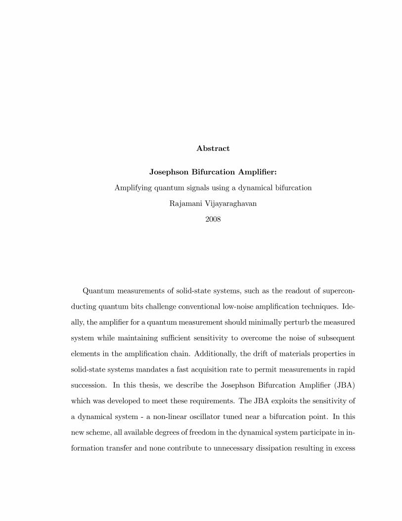
Abstract
Josephson Bifurcation Ampli�er:
Amplifying quantum signals using a dynamical bifurcation
Rajamani Vijayaraghavan
2008
Quantum measurements of solid-state systems, such as the readout of supercon-
ducting quantum bits challenge conventional low-noise ampli�cation techniques. Ide-
ally, the ampli�er for a quantummeasurement should minimally perturb the measured
system while maintaining su¢ cient sensitivity to overcome the noise of subsequent
elements in the ampli�cation chain. Additionally, the drift of materials properties in
solid-state systems mandates a fast acquisition rate to permit measurements in rapid
succession. In this thesis, we describe the Josephson Bifurcation Ampli�er (JBA)
which was developed to meet these requirements. The JBA exploits the sensitivity of
a dynamical system - a non-linear oscillator tuned near a bifurcation point. In this
new scheme, all available degrees of freedom in the dynamical system participate in in-
formation transfer and none contribute to unnecessary dissipation resulting in excess

noise. We have used a superconducting tunnel junction, also known as a Josephson
junction to construct our non-linear oscillator. The Josephson junction is the only
electronic circuit element which remains non-linear and non-dissipative at arbitrarily
low temperatures. This thesis will describe the theory and experiments demonstrat-
ing bifurcation ampli�cation in the JBA and its application to the measurement of
superconducting quantum bits. By describing the JBA as a parametrically driven
oscillator, we will demonstrate that the ultimate sensitivity of the JBA is limited
only by quantum �uctuations. Using this treatment, we will identify the connection
between the four main aspects of working with a dynamical bifurcation: parametric
ampli�cation, squeezing, quantum activation and the Dynamical Casimir E¤ect.
Josephson Bifurcation Ampli�er:
Amplifying quantum signals using a dynamical bifurcation
A Dissertation
Presented to the Faculty of the Graduate School
of
Yale University
in Candidacy for the Degree of
Doctor of Philosophy
by
Rajamani Vijayaraghavan
Dissertation Director: Professor Michel H. Devoret
May 2008
Copyright c 2008 by Rajamani Vijayaraghavan
All rights reserved.
Acknowledgements
Numerous people have played a role in the success of the work described in this thesis
and I will try my best to thank them all.
I would like to begin by thanking my advisor, Prof. Michel Devoret for giving me
a chance to work in his research group - the QuLab. His willingness to devote a lot of
time to his students has always been extremely bene�cial to me, especially during my
early days in the group. Right from the very beginning, Michel gave me the freedom
to be creative in coming up with solutions to the problems we were trying to tackle
in our group. The development of the Josephson Bifurcation Ampli�er (JBA), the
main subject of this thesis was a direct consequence. I am thankful for his continued
guidance throughout the course of my PhD and for instilling in me the importance
of being thorough in the research. I am also extremely grateful for his patience and
support during the writing of my thesis and for reading the manuscript in great detail.
A major part of the experimental work on the JBA was done under the direct
guidance of Irfan Siddiqi who was a post-doctoral researcher in the group and an
experimentalist par excellence. I would like to thank him for teaching me everything
I know about microwave circuit design and cryogenics. His ability to troubleshoot
noise issues in the setup always amazed me. He was also a great friend and the often
monotonous data taking procedure would not have been as much fun without his
1

2
company. A special thanks is also due to Etienne Boaknin, another post-doctoral
associate who developed the lossy "chocolate" �lters which proved critical for imple-
menting the ultra-low noise setup. I would also like to thank Philippe Hya�l for his
assistance in the quantum escape measurements.
A big thanks to the fabrication team which was led by Frederic Pierre and Chris
Wilson during the early days and then taken over by Michael Metcalfe and Chad
Rigetti. All the devices measured during the course of my PhD were fabricated
by them. I would like to thank them for teaching me some of the nuances of the
fabrication procedure as well. I would also like to thank Luigi Frunzio, the ultimate
authority on device fabrication for his assistance in the various fabrication projects.
A special thanks is also due to him for reading my thesis in great detail and providing
suggestions for improvement.
I am extremely grateful to Prof. Daniel Prober for allowing us access to the
resources in his lab. The early work on the JBA was entirely done in his lab. I would
also like to thank him for his role as the Chair of the Applied Physics deparment
in maintaining an enjoyable and productive work enviroment. Thank are also due
to the other members of his lab for their help and support. I would like to thank
Prof. Robert Schoelkopf who along with Prof. Prober served on my thesis committee.
His expertise on designing experiments at microwave frequencies has been extremely
bene�cial to me. I would also like to thank him for numerous discussion on ampli�ers,
especially concerning their noise performance. A big thanks to all the members of his
lab with whom we closely collaborated. The fact that we shared the lab space with
them led to an exciting working enviroment.
Prof. Steven Girvin and his team of theorists have been a great source help in
3
understanding the physics of the JBA. I would like to thank Prof. Girvin for many
useful discussions and his special ability to interface between theory and experiments.
Thanks are also due to K. Sengupta for his work on quantum langevin simulations of
the JBA, Alexandre Blais for his work on the back-action of the JBA on the qubit and
Jay Gambetta for helping us undertand the squeezing e¤ects in the JBA. A special
thanks to Vladimir Manucharyan, a member of our lab, for numerous discussions on
the theory of microwave bifurcations and help with various calculations. Thanks are
also due to the newer members of QuLab: Nicolas, Markus, Flavius and Nick for their
help.
A special thanks to all the administrative sta¤ - Jayne Miller, Pat Brodka, Maria
Gubitosi, Theresa Evangeliste and Giselle DeVito for their hard work in ensuring the
smooth functioning of the group. I would also like to thank Cara Gibilisco for her
prompt assistance in various administrative matters.
Outside of Yale, I would like to thank members of the Quantronics group at Saclay
for their assistance in the design of the quantronium. Thanks are also due to Prof.
Mark Dykman at Michigan State University for being the external reader and also
for his assistance in understanding the physics of driven, non-linear systems. I would
also like to thank all my teachers, especially Dr. Bikram Phookun and Dr. Pratibha
Jolly who have been instrumental in my decision to pursue a career in Physics.
Life at Yale would have been extremely dull without all my friends. I would like
to thank them all for their friendship and support during the last several years. A
special thanks to Dhruv, who has always been there during the good and bad times
and a constant source of encouragement. I would also like to thank Sahar, Josiah,
Athena and Isaac for providing me a place in their home during the last few months

4
at Yale.
Finally, and most importantly, I would like to thank my family - Amma, Appa,
Athai, Mohan and Vasu. Without their love and support, I could have never dreamed
of embarking on this journey and I dedicate this thesis to them.
Contents
1 Introduction 21
1.1 Ampli�cation and quantum limited detection . . . . . . . . . 23
1.2 Amplifying using a bifurcation . . . . . . . . . . . . . . . . . . 26
1.2.1 The Josephson junction . . . . . . . . . . . . . . . . . . . . . 27
1.2.2 Bifurcation in a RF driven Josephson oscillator . . . . . . . . 28
1.2.3 Operating principle of the JBA . . . . . . . . . . . . . . . . . 31
1.3 Superconducting quantum circuits . . . . . . . . . . . . . . . . 32
1.4 Summary of key results . . . . . . . . . . . . . . . . . . . . . . . 40
1.4.1 JBA Measurements . . . . . . . . . . . . . . . . . . . . . . . . 40
1.4.2 Qubit measurements . . . . . . . . . . . . . . . . . . . . . . . 42
1.4.3 Escape measurements in the quantum regime . . . . . . . . . 47
1.5 Thesis overview . . . . . . . . . . . . . . . . . . . . . . . . . . . . 52
2 Josephson Bifurcation Ampli�er: Theory 56
2.1 General properties of a driven non-linear oscillator . . . . . 56
2.2 Josephson junction oscillator . . . . . . . . . . . . . . . . . . . 59
2.2.1 Bistability in driven Josephson oscillator . . . . . . . . . . . . 59
5
CONTENTS 6
2.2.2 Dynamics in quadrature amplitude plane . . . . . . . . . . . . 66
2.3 Josephson Bifurcation Ampli�er . . . . . . . . . . . . . . . . . 69
2.3.1 Operating principle . . . . . . . . . . . . . . . . . . . . . . . . 69
2.3.2 Transition Rates . . . . . . . . . . . . . . . . . . . . . . . . . 73
2.3.3 Measurement sensitivity . . . . . . . . . . . . . . . . . . . . . 77
3 Josephson Bifurcation Ampli�er: Experiments 81
3.1 Experimental setup . . . . . . . . . . . . . . . . . . . . . . . . . . 81
3.2 Frequency domain measurements . . . . . . . . . . . . . . . . . 86
3.2.1 Linear resonance . . . . . . . . . . . . . . . . . . . . . . . . . 86
3.2.2 Non-linear resonance . . . . . . . . . . . . . . . . . . . . . . . 90
3.3 Time domain measurements . . . . . . . . . . . . . . . . . . . . 92
3.3.1 Hysteresis and bistability in the JBA . . . . . . . . . . . . . . 93
3.3.2 JBA as a readout . . . . . . . . . . . . . . . . . . . . . . . . . 96
3.4 Microwave design considerations . . . . . . . . . . . . . . . . . 98
4 JBA as a qubit readout 105
4.1 The Cooper pair box . . . . . . . . . . . . . . . . . . . . . . . . . 105
4.1.1 Hamiltonian in charge basis . . . . . . . . . . . . . . . . . . . 107
4.1.2 Hamiltonian in phase basis . . . . . . . . . . . . . . . . . . . . 108
4.1.3 The split Cooper pair box . . . . . . . . . . . . . . . . . . . . 110
4.2 The quantronium . . . . . . . . . . . . . . . . . . . . . . . . . . . 112
4.2.1 Quantronium as a quantum bit . . . . . . . . . . . . . . . . . 113
4.2.2 Readout strategies . . . . . . . . . . . . . . . . . . . . . . . . 117
4.3 Measuring the quantronium with the JBA . . . . . . . . . . . 119

CONTENTS 7
4.3.1 E¤ective Hamiltonian . . . . . . . . . . . . . . . . . . . . . . . 119
4.3.2 Measurement protocol . . . . . . . . . . . . . . . . . . . . . . 122
4.3.3 E¤ective critical current . . . . . . . . . . . . . . . . . . . . . 124
4.3.4 Qubit readout optimization . . . . . . . . . . . . . . . . . . . 128
4.3.5 Qubit readout performance . . . . . . . . . . . . . . . . . . . 130
4.4 Numerical simulations . . . . . . . . . . . . . . . . . . . . . . . . 132
5 Qubit coherence measurements 136
5.1 Measurement setup . . . . . . . . . . . . . . . . . . . . . . . . . . 136
5.2 Ground state characterization . . . . . . . . . . . . . . . . . . . 140
5.3 Spectroscopy . . . . . . . . . . . . . . . . . . . . . . . . . . . . . . 142
5.4 Time domain measurements . . . . . . . . . . . . . . . . . . . . 145
5.5 Readout �delity . . . . . . . . . . . . . . . . . . . . . . . . . . . . 150
6 Qubit readout performance 155
6.1 Quantum non-demolition readout using a JBA . . . . . . . . 156
6.2 Information �ow during qubit measurement . . . . . . . . . . 158
6.2.1 Multiple pulse measurements . . . . . . . . . . . . . . . . . . 158
6.2.2 AC Stark shift of qubit . . . . . . . . . . . . . . . . . . . . . . 162
6.2.3 Quantifying the losses during readout . . . . . . . . . . . . . . 165
6.3 Characterizing the qubit environment . . . . . . . . . . . . . . 171
6.4 Approaching a single-shot readout . . . . . . . . . . . . . . . . 176
7 Quantum escape and parametric ampli�cation:Theory 182
7.1 Input-Output theory . . . . . . . . . . . . . . . . . . . . . . . . . 183
CONTENTS 8
7.1.1 Harmonic oscillator coupled to a transmission line . . . . . . . 184
7.1.2 Escape in current-biased Josephson junction . . . . . . . . . . 189
7.2 Escape dynamics in the JBA . . . . . . . . . . . . . . . . . . . 195
7.2.1 Parametric ampli�er description of the JBA . . . . . . . . . . 195
7.2.2 Solutions in the frequency domain . . . . . . . . . . . . . . . . 199
7.2.3 Quadrature variables . . . . . . . . . . . . . . . . . . . . . . . 202
7.2.4 Escape rates . . . . . . . . . . . . . . . . . . . . . . . . . . . . 204
7.3 Parametric ampli�cation in the JBA . . . . . . . . . . . . . . 210
7.3.1 Parametric gain . . . . . . . . . . . . . . . . . . . . . . . . . . 211
7.3.2 Noise temperature and the quantum limit . . . . . . . . . . . 212
7.3.3 Squeezing . . . . . . . . . . . . . . . . . . . . . . . . . . . . . 215
8 Quantum escape and parametric ampli�cation:Experiments 218
8.1 Dynamical Casimir E¤ect . . . . . . . . . . . . . . . . . . . . . . 220
8.2 Quantum escape measurements . . . . . . . . . . . . . . . . . . 222
8.2.1 Switching measurements in the JBA . . . . . . . . . . . . . . 222
8.2.2 Combined RF and DC biasing scheme . . . . . . . . . . . . . 224
8.2.3 Measuring escape rates . . . . . . . . . . . . . . . . . . . . . . 228
8.2.4 Temperature dependence . . . . . . . . . . . . . . . . . . . . . 230
8.2.5 Detuning dependence . . . . . . . . . . . . . . . . . . . . . . . 233
8.3 Parametric ampli�cation in the JBA . . . . . . . . . . . . . . 237
8.3.1 Measurement protocol . . . . . . . . . . . . . . . . . . . . . . 237
8.3.2 Gain and noise temperature . . . . . . . . . . . . . . . . . . . 239
8.3.3 Squeezing measurements . . . . . . . . . . . . . . . . . . . . . 244
CONTENTS 9
9 Future directions 247
9.1 Evolution of the JBA . . . . . . . . . . . . . . . . . . . . . . . . 247
9.2 Back-action of the bifurcation readout on a qubit . . . . . . 249
9.3 Josephson Parametric Converter . . . . . . . . . . . . . . . . . 250
10Conclusions 252
Appendices 255
A JBA formulae 255
B Mathematica formulae 257
C Numerical simulations 259
C.1 Equations of motion . . . . . . . . . . . . . . . . . . . . . . . . . 260
List of Figures
1.1 General ampli�cation process . . . . . . . . . . . . . . . . . . . . . . 24
1.2 Josephson tunnel junction . . . . . . . . . . . . . . . . . . . . . . . . 27
1.3 Non-linear resonance curves in a driven Josephson oscillator. . . . . 30
1.4 Schematic of bifurcation ampli�er . . . . . . . . . . . . . . . . . . . . 31
1.5 Di¤erent varieties of superconducting qubits. . . . . . . . . . . . . . . 36
1.6 The original quantronium qubit. . . . . . . . . . . . . . . . . . . . . . 37
1.7 Phase response of JBA as a function of drive frequency and power . . 41
1.8 Quantronium qubit readout using a JBA . . . . . . . . . . . . . . . . 43
1.9 Summary of qubit coherence measurements . . . . . . . . . . . . . . . 45
1.10 Escape temperature v.s. bath temperature for dynamical and static
escape. . . . . . . . . . . . . . . . . . . . . . . . . . . . . . . . . . . . 51
2.1 Simple pendulum as a non-linear oscillator . . . . . . . . . . . . . . . 57
2.2 Linear v.s. non-linear resonance . . . . . . . . . . . . . . . . . . . . . 58
2.3 Driven Josephson oscillator circuit . . . . . . . . . . . . . . . . . . . . 59
2.4 Steady state solutions of the driven non-linear oscillator . . . . . . . . 63
2.5 Bistability diagram . . . . . . . . . . . . . . . . . . . . . . . . . . . . 65
10

LIST OF FIGURES 11
2.6 Poincaré sections of an RF driven Josephson junction. . . . . . . . . . 68
2.7 JBA operating principle . . . . . . . . . . . . . . . . . . . . . . . . . 70
2.8 Switching probability curves . . . . . . . . . . . . . . . . . . . . . . . 72
2.9 Metapotential for the e¤ective slow coordinate. . . . . . . . . . . . . . 75
3.1 Optical image of chip capacitor and SEM image of Josephson junction 83
3.2 Pictures of microwave setup and sample box . . . . . . . . . . . . . . 84
3.3 Schematic of the measurement setup . . . . . . . . . . . . . . . . . . 85
3.4 Phase response of JBA in linear regime. . . . . . . . . . . . . . . . . 87
3.5 Extracting JBA resonator parameters . . . . . . . . . . . . . . . . . . 89
3.6 Phase response of JBA as a function of drive frequency and power . . 91
3.7 Hysteretic response of the JBA . . . . . . . . . . . . . . . . . . . . . 93
3.8 Histograms of the re�ected signal phase . . . . . . . . . . . . . . . . . 95
3.9 Switching probability curves for the JBA . . . . . . . . . . . . . . . . 96
3.10 Linear resonance measurement in a JBA with stray parameters . . . . 98
3.11 Magnitude and phase response of a JBA with stray parameters. . . . 100
3.12 Audio frequency ac resistance of a non-linear oscillator as a function
of drive power at a �xed frequency . . . . . . . . . . . . . . . . . . . 102
4.1 Cooper pair box . . . . . . . . . . . . . . . . . . . . . . . . . . . . . . 106
4.2 Energy levels of the Cooper pair box . . . . . . . . . . . . . . . . . . 109
4.3 Split Cooper pair box . . . . . . . . . . . . . . . . . . . . . . . . . . . 110
4.4 The quantronium circuit . . . . . . . . . . . . . . . . . . . . . . . . . 113
4.5 Bloch sphere representation . . . . . . . . . . . . . . . . . . . . . . . 114
4.6 Quantronium energy levels . . . . . . . . . . . . . . . . . . . . . . . . 116
LIST OF FIGURES 12
4.7 Quantronium with JBA readout . . . . . . . . . . . . . . . . . . . . . 119
4.8 Quantronium loop currents . . . . . . . . . . . . . . . . . . . . . . . . 126
4.9 Quantronium gate and �ux modulations . . . . . . . . . . . . . . . . 127
4.10 Critical current variation in quantronium . . . . . . . . . . . . . . . . 129
4.11 Simulated S-curves for quantronium+JBA. . . . . . . . . . . . . . . . 134
5.1 Schematic of qubit measurement setup . . . . . . . . . . . . . . . . . 137
5.2 Fridge setup for qubit measurements . . . . . . . . . . . . . . . . . . 138
5.3 Ground state properties of the quantronium (sample A) v.s. gate and
�ux bias . . . . . . . . . . . . . . . . . . . . . . . . . . . . . . . . . . 141
5.4 Spectroscopic peaks . . . . . . . . . . . . . . . . . . . . . . . . . . . . 143
5.5 Variation of qubit transition frequency with gate charge . . . . . . . . 144
5.6 Qubit lineshape for sample A . . . . . . . . . . . . . . . . . . . . . . 145
5.7 Rabi oscillation data for sample B . . . . . . . . . . . . . . . . . . . . 146
5.8 T1 data for sample B . . . . . . . . . . . . . . . . . . . . . . . . . . . 148
5.9 Ramsey fringe data for sample B . . . . . . . . . . . . . . . . . . . . 149
5.10 Echo data for sample B . . . . . . . . . . . . . . . . . . . . . . . . . . 151
5.11 S-curves for sample B . . . . . . . . . . . . . . . . . . . . . . . . . . . 153
6.1 Multiple readout of qubit state . . . . . . . . . . . . . . . . . . . . . 159
6.2 Two pulse measurements of the qubit state . . . . . . . . . . . . . . . 161
6.3 AC Stark shift of qubit frequency with driving on phase or gate port. 164
6.4 Information �ow during qubit readout . . . . . . . . . . . . . . . . . 166
6.5 Detuning dependence of two pulse measurements . . . . . . . . . . . 168
6.6 Summary of readout induced relaxation as function of drive detuning. 170
LIST OF FIGURES 13
6.7 Spectroscopy data revealing resonances in the qubit environment . . . 172
6.8 Unexpected variation of T1 with gate and �ux bias. . . . . . . . . . . 175
6.9 T1 measured at Stark shifted frequencies . . . . . . . . . . . . . . . . 176
6.10 Exploiting second excited of qubit to enhance readout contrast. . . . 178
7.1 Harmonic oscillator coupled to a transmission line . . . . . . . . . . . 184
7.2 Transmission line equations . . . . . . . . . . . . . . . . . . . . . . . 185
7.3 Input-output relations for circuits . . . . . . . . . . . . . . . . . . . . 186
7.4 DC current biased Josephson junction . . . . . . . . . . . . . . . . . . 189
7.5 Cubic potential and its harmonic approximation . . . . . . . . . . . . 191
7.6 Non-linear resonance curves in a driven Josephson oscillator. . . . . 198
7.7 Gain functions jA (f)j2 and jB (f)j2 . . . . . . . . . . . . . . . . . . . 201
7.8 Noise dynamics in quadrature variable space. . . . . . . . . . . . . . . 203
7.9 Spectrum of the quadrature variables . . . . . . . . . . . . . . . . . . 206
7.10 Computed gain of a parametric ampli�er . . . . . . . . . . . . . . . . 213
7.11 Squeezing spectrum of the output �eld of the JBA . . . . . . . . . . . 216
8.1 Di¤erent schemes to observe the Dynamical Casimir E¤ect . . . . . . 219
8.2 Combined biasing scheme for single-ended RF and di¤erential DC signals.225
8.3 A picture of the DC and RF circuitry . . . . . . . . . . . . . . . . . . 227
8.4 Measurements of escape rate in the JBA at di¤erent temperatures. . . 229
8.5 A plot of TDCesc vs T in a DC current biased Josephson junction. . . . 231
8.6 A plot of TRFesc vs T in the JBA . . . . . . . . . . . . . . . . . . . . . 232
8.7 Frequency dependence of RF escape temperature . . . . . . . . . . . 234
8.8 Phase diagram of the non-linear resonance in a JBA. . . . . . . . . . 236
LIST OF FIGURES 14
8.9 Measurement protocol for parametric ampli�er . . . . . . . . . . . . . 238
8.10 Gain and output noise in a PARAMP . . . . . . . . . . . . . . . . . . 240
8.11 PARAMP gain near critical point. . . . . . . . . . . . . . . . . . . . . 241
8.12 Gain and noise temperature in a PARAMP . . . . . . . . . . . . . . . 243
8.13 Squeezing in the JBA . . . . . . . . . . . . . . . . . . . . . . . . . . . 245
9.1 Optical image of a Cavity Bifurcation Ampli�er . . . . . . . . . . . . 248
9.2 Schematic of Josephson Parametric Converter . . . . . . . . . . . . . 250
C.1 Full circuit model of the JBA . . . . . . . . . . . . . . . . . . . . . . 259
List of Tables
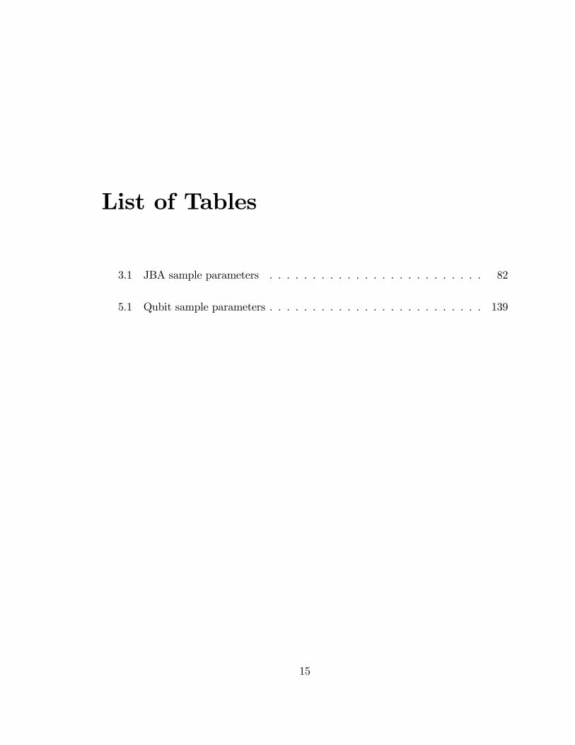
3.1 JBA sample parameters . . . . . . . . . . . . . . . . . . . . . . . . . 82
5.1 Qubit sample parameters . . . . . . . . . . . . . . . . . . . . . . . . . 139
15

List of symbols and abbreviations
(�) Relative detuning � = 1� !d=!p
(�N) Reduced noise intensity
(�) Reduced drive power in a driven du¢ ng oscillator
(��B) Upper and lower bifurcation points in reduced units
(�c) Critical value of �, � > �c for bistability
(�) Gauge invariant phase di¤erence across Josephson junction
(�k) In-phase amplitude of oscillations in the JBA
(�?) Quadrature-phase amplitude of oscillations in the JBA
(�m) Superconducting phase drop due to magnetic �ux
(�R) Superconducting phase drop across readout junction
( ) Coe¢ cient of �rst non-linear term in Josephson oscillator = !2p=6
(�) Oscillator damping rate
(�R) Re�ection coe¢ cient
(�c) Readout contrast
16
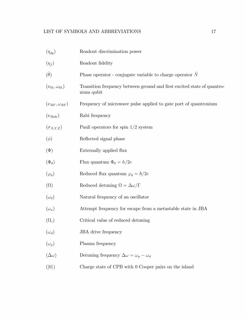
LIST OF SYMBOLS AND ABBREVIATIONS 17
(�dp) Readout discrimination power
(�f) Readout �delity
(�) Phase operator - conjugate variable to charge operator N
(�01; !01) Transition frequency between ground and �rst excited state of quantro-nium qubit
(�RF ; !RF ) Frequency of microwave pulse applied to gate port of quantronium
(�Rabi) Rabi frequency
(�X;Y;Z) Pauli operators for spin 1=2 system
(�) Re�ected signal phase
(�) Externally applied �ux
(�0) Flux quantum �0 = h=2e
('0) Reduced �ux quantum '0 = ~=2e
() Reduced detuning = �!=�
(!0) Natural frequency of an oscillator
(!a) Attempt frequency for escape from a metastable state in JBA
(c) Critical value of reduced detuning
(!d) JBA drive frequency
(!p) Plasma frequency
(�!) Detuning frequency �! = !p � !d
(j0i) Charge state of CPB with 0 Cooper pairs on the island
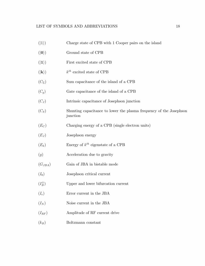
LIST OF SYMBOLS AND ABBREVIATIONS 18
(j1i) Charge state of CPB with 1 Cooper pairs on the island
(j0i) Ground state of CPB
(j1i) First excited state of CPB
(jki) kth excited state of CPB
(C�) Sum capacitance of the island of a CPB
(Cg) Gate capacitance of the island of a CPB
(CJ) Intrinsic capacitance of Josephson junction
(CS) Shunting capacitance to lower the plasma frequency of the Josephsonjunction
(EC) Charging energy of a CPB (single electron units)
(EJ) Josephson energy
(Ek) Energy of kth eigenstate of a CPB
(g) Acceleration due to gravity
(GJBA) Gain of JBA in bistable mode
(I0) Josephson critical current
(I�B ) Upper and lower bifurcation current
(Ie) Error current in the JBA
(IN) Noise current in the JBA
(IRF ) Amplitude of RF current drive
(kB) Boltzmann constant

LIST OF SYMBOLS AND ABBREVIATIONS 19
(LJ) Josephson inductance
(LS) Stray inductance in the microfabricated capacitor
(Ng) Reduced gate polarization charge on the island of CPB
(jNi) Charge state with N Cooper pairs on the island of a CPB
(N) Operator for number of Cooper pairs on the island of CPB
(OH) High amplitude state of the JBA
(OL) High amplitude state of the JBA
(OS) Unstable state (saddle point) of the JBA
(Pswitch) Probability of switching from OL to OH
(Q) Quality factor of a resonator
(R) Source resistance of current source driving the JBA
(RS) Stray resistance in the microfabricated capacitor
(SI0) Critical current sensitivity of JBA in A /pHz
(T ) Temperature
(Techo) Echo time for a qubit
(T') Pure dephasing time for a qubit
(T1) Relaxation time for a qubit
(T2) Total dephasing time for a qubit
(TN) Noise temperature of an ampli�er
(u) Slow, complex amplitude of oscillator response
LIST OF SYMBOLS AND ABBREVIATIONS 20
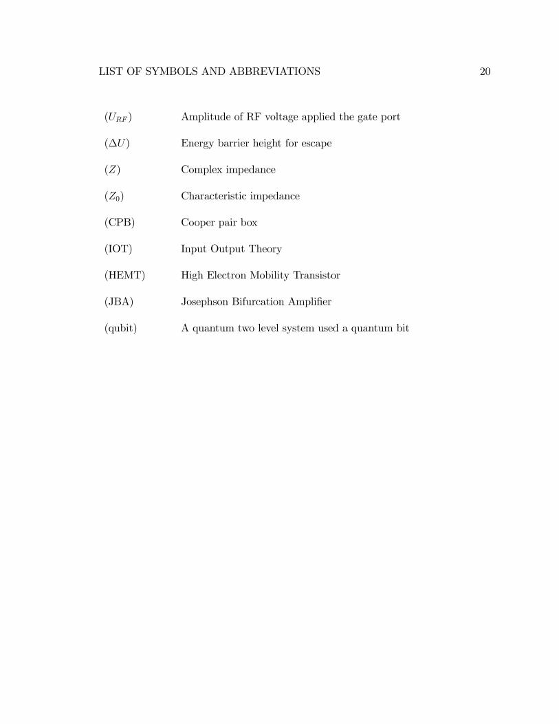
(URF ) Amplitude of RF voltage applied the gate port
(�U) Energy barrier height for escape
(Z) Complex impedance
(Z0) Characteristic impedance
(CPB) Cooper pair box
(IOT) Input Output Theory
(HEMT) High Electron Mobility Transistor
(JBA) Josephson Bifurcation Ampli�er
(qubit) A quantum two level system used a quantum bit

Chapter 1
Introduction
Ampli�cation using a laser, a maser or a transistor is based on energizing many
microscopic systems. Atoms in a cavity or conduction electrons in a channel are some
typical examples. Each microscopic degree of freedom is weakly coupled to the input
signal. The overall power gain of the system, which is determined by the product
of the number of active microscopic systems and their individual response to the
input parameter, can be quite substantial. However, noise can result from the lack
of control of each individual microscopic system. In this thesis, we explore another
strategy for ampli�cation. We utilize a system with only one, well controlled degree
of freedom, which is driven to a high level of excitation. The input signal is coupled
parametrically to the system and in�uences its dynamics leading to ampli�cation. The
superconducting quantum interference device (SQUID) [1] and the radio frequency
single electron transistor (RF-SET) [2] are two well known devices which use this
strategy. The system we have chosen is a driven, non-linear oscillator biased near
a dynamical bifurcation. We call this device the Josephson Bifurcation Ampli�er
(JBA) since the non-linear oscillator is constructed using a Josephson junction [3].
21

CHAPTER 1. INTRODUCTION 22
The main advantage of the JBA over the SQUID and the RF-SET is that there is no
intrinsic dissipation resulting in minimum noise and back-action.
In this dissertation, we exploit the non-linearity of a Josephson junction [3], which
is a superconducting tunnel junction and therefore the only electronic circuit element
which remains non-linear and non-dissipative at arbitrary low temperatures. The pri-
mary goal of the JBA was to readout the quantum state of superconducting quantum
bits (qubits). Superconducting qubits are electronic circuits made to behave like arti-
�cial atoms [4, 5, 6, 7]. We map the two quantum states of the qubit to two di¤erent
driven states of the non-linear oscillator which is bistable under appropriate driving
conditions. Bistability has been extensively studied in non-linear optical systems too,
but they have always been plagued by dissipation in the non-linear medium (see [8]
for a review). We have also explored the possibility of using the JBA as a linear,
phase preserving, parametric ampli�er [9] operating at the quantum limit [10].
This work brings together ideas from di¤erent areas of physics like non-linear dy-
namics, non-equilibrium statistical mechanics, quantum measurements, quantum lim-
ited ampli�cation and experimental techniques like cryogenics, ultra-low noise mea-
surements and microwave engineering. In this introduction, we will �rst discuss the
ampli�cation process and the restrictions placed on it by quantum mechanics. This
will be followed by a discussion on the use of bifurcations for ampli�cation. We will
then brie�y talk about superconducting quantum circuits and highlight the challenges
in reading out their quantum state. Finally, we will summarize the key experimental
results of the work carried out for this dissertation.

CHAPTER 1. INTRODUCTION 23
1.1 Ampli�cation and quantum limited detection
Ampli�ers are an important part of any experiment carrying out high precision mea-
surements. In particular, cryogenic, low noise ampli�ers working in the microwave
domain have recently found a growing number of applications in mesoscopic physics,
astrophysics and particle detector physics [11, 12]. An ampli�er is needed in order
to raise the level of a weak input signal to a macroscopic level so that it can over-
come the noise of conventional signal processing circuitry. The room temperature
signal processing electronics are generally quite noisy and cannot be directly used to
measure very weak signals from typical cryogenic, mesoscopic physics experiments.
A sensitive, low noise ampli�er is required to interface the extremely weak signals
coming from an experiment to the noisy room temperature electronics.
A linear ampli�er is one whose output is linearly related to its input signal. This
de�nition is quite broad and includes both frequency-converting ampli�ers, whose
output is at a frequency di¤erent from the input frequency, and phase-sensitive am-
pli�ers, whose response depends on the phase of the input signal. We will be mostly
considering phase-insensitive linear ampli�ers which preserve the phase of the input
signal.
An ampli�er must have two important properties. Firstly, the output power of
the ampli�er should be large enough, so that any further processing of the signal
does not degrade the signal to noise ratio. At the same time, the ampli�er must
add the minimum possible noise to the signal during the ampli�cation process. The
ampli�cation process in general degrades the signal-to-noise ratio. This is shown
schematically in Fig. 1.1. Quantum mechanics places a restriction on this added
noise. When this is quantum minimum is achieved, the ampli�er is labeled quan-
CHAPTER 1. INTRODUCTION 24
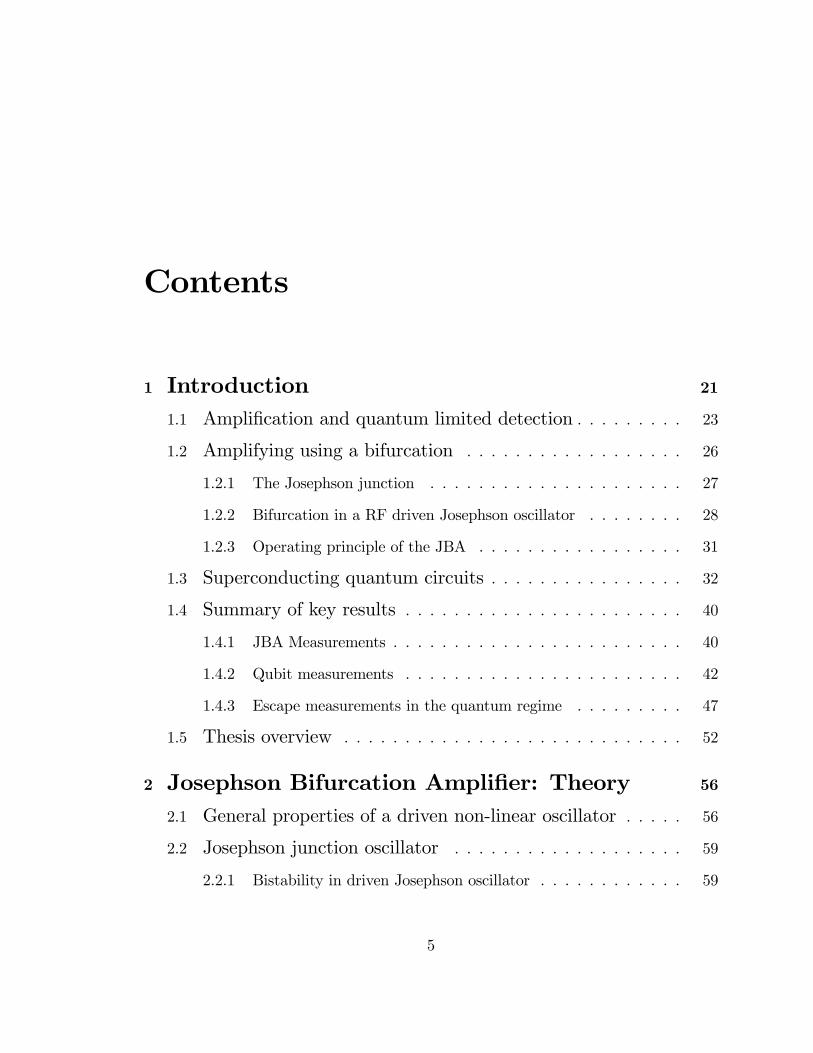
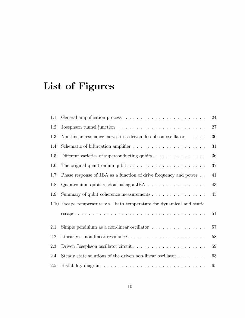
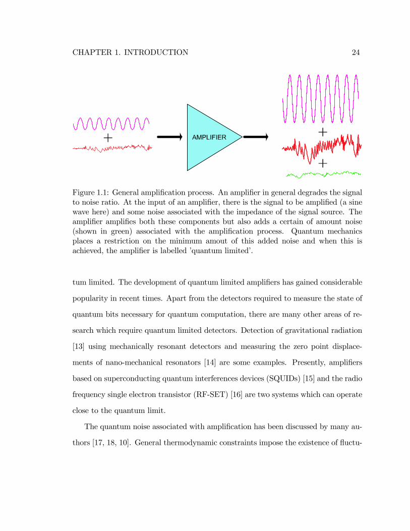
Figure 1.1: General ampli�cation process. An ampli�er in general degrades the signalto noise ratio. At the input of an ampli�er, there is the signal to be ampli�ed (a sinewave here) and some noise associated with the impedance of the signal source. Theampli�er ampli�es both these components but also adds a certain of amount noise(shown in green) associated with the ampli�cation process. Quantum mechanicsplaces a restriction on the minimum amout of this added noise and when this isachieved, the ampli�er is labelled �quantum limited�.
tum limited. The development of quantum limited ampli�ers has gained considerable
popularity in recent times. Apart from the detectors required to measure the state of
quantum bits necessary for quantum computation, there are many other areas of re-
search which require quantum limited detectors. Detection of gravitational radiation
[13] using mechanically resonant detectors and measuring the zero point displace-
ments of nano-mechanical resonators [14] are some examples. Presently, ampli�ers
based on superconducting quantum interferences devices (SQUIDs) [15] and the radio
frequency single electron transistor (RF-SET) [16] are two systems which can operate
close to the quantum limit.
The quantum noise associated with ampli�cation has been discussed by many au-
thors [17, 18, 10]. General thermodynamic constraints impose the existence of �uctu-

CHAPTER 1. INTRODUCTION 25
ations not only for dissipation but for ampli�cation processes as well. In the limit of
zero temperature, these thermal �uctuations reduce to quantum �uctuations which
are governed by the Heisenberg�s uncertainty principle. These quantum �uctuations
determine the ultimate performance of any ampli�er and hence play an important
role in high precision measurements. The exact manifestation of this quantum limit
depends on the kind of measurement being performed [18]. Quantum mechanics does
not impose any restriction on the ultimate precision of a single measurement of a
single quantity (say, position of a particle), but only on the combined precision of two
conjugate variables (for example, position and momentum). For the typical case of
continuous measurement of the amplitude and phase of a sinusoidal signal, the min-
imum noise energy (EN) an ampli�er must add to a signal at frequency !s is given
by
EN = kBTN = ~!s=2: (1.1)
Here EN is referred to the input. This is often called the standard quantum limit and
applies to phase-preserving ampli�ers. The minimum noise energy (EN) can also be
expressed as a noise temperature (TN) as shown in equation 1.1. The above limit has
been derived in various ways by di¤erent authors [17, 18, 10]. A more recent analysis
incorporates ideas from quantum network theory where ampli�cation is described
as an e¤ective scattering process [19, 20]. In this treatment, signals travel to and
from the ampli�er via semi-in�nite transmission lines. The current and voltage along
the line are treated as propagating quantum �elds. The incoming �elds represent the
input signal and �uctuations while the outgoing �elds describe dissipation and output
signals. The commutation properties of the input and output �eld operators lead to
the fact that the ampli�er must add a minimum amount of noise given by equation
CHAPTER 1. INTRODUCTION 26
1.1. We will use this �eld representation to study the quantum behavior of the JBA
in chapter 7.
1.2 Amplifying using a bifurcation
The idea of amplifying signals using a bifurcation has been around for a long time [21,
22]. Any of the di¤erent types of bifurcation could be used, and only the details of the
small signal sensitivity are determined by the type of bifurcation [22]. Bifurcations are
quite common and have been observed in electrical, optical, chemical and biological
systems (see [21] for references). An example of bifurcation ampli�cation in nature is
the ear. It turns out that the cochlea, the hearing organ in our ear, is biased close to a
Hopf bifurcation [23]. This leads to several remarkable properties in our hearing like
compression of dynamic range, in�nitely sharp tuning at zero input and generation
of combination tones. The ear is essentially a non-linear ampli�er, i.e., the response
depends quite strongly on the strength of the input signal. Researchers in robotics
and medical sciences are currently in the process of constructing a hearing sensor
which can mimic the non-linear properties of the cochlea [24].
Bifurcation ampli�cation is also not new to the �eld of superconducting device
physics. The well known Josephson parametric ampli�ers [9] also exploit the near-
ness to a bifurcation. These devices are capable of achieving large gain and can show
interesting quantum e¤ects like squeezing of noise below the vacuum �oor [25]. Tra-
ditionally, they have always been plagued by the "noise rise" problem where the noise
tends to grow with the gain. It has been suggested that this is due to instabilities
in dynamical systems operating near a bifurcation point [26]. In the JBA, we use
this instability to our advantage to make a highly sensitive threshold detector. The
CHAPTER 1. INTRODUCTION 27
main application of this mode of operation of the JBA is to measure the state of
superconducting quantum bits (see section 1.3). We should point out that the JBA
can also be operated as a parametric ampli�er (see chapter 7). We now discuss how
we can access a bifurcation in a non-linear oscillator made with a Josephson junction.
1.2.1 The Josephson junction
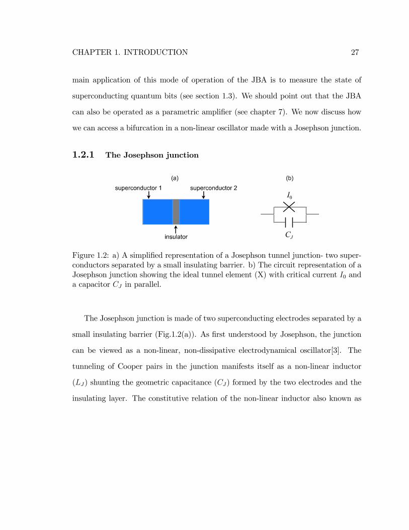
Figure 1.2: a) A simpli�ed representation of a Josephson tunnel junction- two super-conductors separated by a small insulating barrier. b) The circuit representation of aJosephson junction showing the ideal tunnel element (X) with critical current I0 anda capacitor CJ in parallel.
The Josephson junction is made of two superconducting electrodes separated by a
small insulating barrier (Fig.1.2(a)). As �rst understood by Josephson, the junction
can be viewed as a non-linear, non-dissipative electrodynamical oscillator[3]. The
tunneling of Cooper pairs in the junction manifests itself as a non-linear inductor
(LJ) shunting the geometric capacitance (CJ) formed by the two electrodes and the
insulating layer. The constitutive relation of the non-linear inductor also known as

CHAPTER 1. INTRODUCTION 28
the Josephson relations, can be written as
I(t) = I0 sin � (t) (1.2)
� (t) =
Z t
�1dt0V (t0)='0
where I(t), � (t) and V (t) are the current, gauge-invariant phase-di¤erence and voltage
across the junction respectively. The parameter I0 is the junction critical current and
is the maximum current that can passed through the junction in its superconducting
state. Here, '0 = ~=2e is the reduced �ux quantum. For small oscillation amplitude
(j�j << 1), the frequency of oscillation for zero bias current is given by the so-called
plasma frequency
!p =1pLJCJ
(1.3)
where
LJ ='0I0
(1.4)
is e¤ective junction inductance.
1.2.2 Bifurcation in a RF driven Josephson oscillator
The di¤erential equation describing the dynamics of a Josephson junction oscillator
driven with a RF current is given by
CS'0d2�(t)
dt2+'0R
d�(t)
dt+ I0 sin(�(t)) = IRF cos (!dt) (1.5)
Here is � is the gauge-invariant phase di¤erence across the junction, I0 is the critical
current of the junction, CS is the shunt capacitance, R is the source impedance of the
CHAPTER 1. INTRODUCTION 29
current drive and provides damping, !d is the drive frequency and '0 = ~=2e is the
reduced �ux quantum. In our experiments, we always shunt the Josephson junction
with an additional capacitance (CS >> CJ) to reduce the plasma frequency (see
section 2.2). The sine term, whose origin is the current-phase relation of the Josephson
junction (1.2), is the source of non-linearity in the oscillator. Under appropriate
driving conditions, this non-linear oscillator can have two steady driven states di¤ering
in amplitude and phase[27, 28]. We will call these two states as the low amplitude
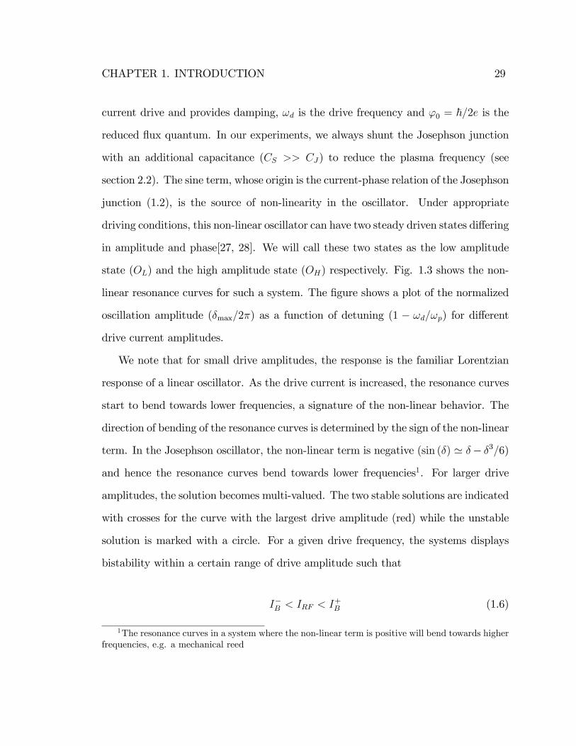
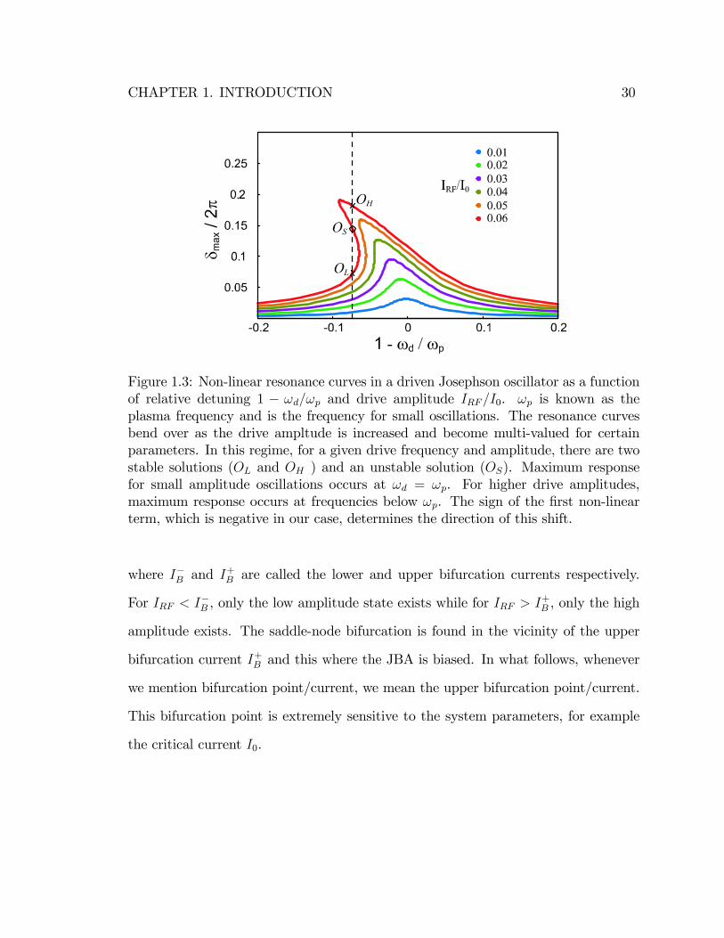
state (OL) and the high amplitude state (OH) respectively. Fig. 1.3 shows the non-
linear resonance curves for such a system. The �gure shows a plot of the normalized
oscillation amplitude (�max=2�) as a function of detuning (1 � !d=!p) for di¤erent
drive current amplitudes.
We note that for small drive amplitudes, the response is the familiar Lorentzian
response of a linear oscillator. As the drive current is increased, the resonance curves
start to bend towards lower frequencies, a signature of the non-linear behavior. The
direction of bending of the resonance curves is determined by the sign of the non-linear
term. In the Josephson oscillator, the non-linear term is negative (sin (�) ' �� �3=6)
and hence the resonance curves bend towards lower frequencies1. For larger drive
amplitudes, the solution becomes multi-valued. The two stable solutions are indicated
with crosses for the curve with the largest drive amplitude (red) while the unstable
solution is marked with a circle. For a given drive frequency, the systems displays
bistability within a certain range of drive amplitude such that
I�B < IRF < I+B (1.6)
1The resonance curves in a system where the non-linear term is positive will bend towards higherfrequencies, e.g. a mechanical reed
CHAPTER 1. INTRODUCTION 30
Figure 1.3: Non-linear resonance curves in a driven Josephson oscillator as a functionof relative detuning 1 � !d=!p and drive amplitude IRF=I0. !p is known as theplasma frequency and is the frequency for small oscillations. The resonance curvesbend over as the drive ampltude is increased and become multi-valued for certainparameters. In this regime, for a given drive frequency and amplitude, there are twostable solutions (OL and OH ) and an unstable solution (OS). Maximum responsefor small amplitude oscillations occurs at !d = !p. For higher drive amplitudes,maximum response occurs at frequencies below !p. The sign of the �rst non-linearterm, which is negative in our case, determines the direction of this shift.
where I�B and I+B are called the lower and upper bifurcation currents respectively.
For IRF < I�B , only the low amplitude state exists while for IRF > I+B , only the high
amplitude exists. The saddle-node bifurcation is found in the vicinity of the upper
bifurcation current I+B and this where the JBA is biased. In what follows, whenever
we mention bifurcation point/current, we mean the upper bifurcation point/current.
This bifurcation point is extremely sensitive to the system parameters, for example
the critical current I0.
CHAPTER 1. INTRODUCTION 31
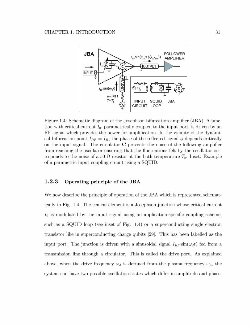
Figure 1.4: Schematic diagram of the Josephson bifurcation ampli�er (JBA). A junc-tion with critical current I0, parametrically coupled to the input port, is driven by anRF signal which provides the power for ampli�cation. In the vicinity of the dynami-cal bifurcation point IRF = IB, the phase of the re�ected signal � depends criticallyon the input signal. The circulator C prevents the noise of the following ampli�erfrom reaching the oscillator ensuring that the �uctuations felt by the oscillator cor-responds to the noise of a 50 resistor at the bath temperature Tb. Inset: Exampleof a parametric input coupling circuit using a SQUID.
1.2.3 Operating principle of the JBA
We now describe the principle of operation of the JBA which is represented schemat-
ically in Fig. 1.4. The central element is a Josephson junction whose critical current
I0 is modulated by the input signal using an application-speci�c coupling scheme,
such as a SQUID loop (see inset of Fig. 1.4) or a superconducting single electron
transistor like in superconducting charge qubits [29]. This has been labelled as the
input port. The junction is driven with a sinusoidal signal IRF sin(!dt) fed from a
transmission line through a circulator. This is called the drive port. As explained
above, when the drive frequency !d is detuned from the plasma frequency !p, the
system can have two possible oscillation states which di¤er in amplitude and phase.
CHAPTER 1. INTRODUCTION 32
Starting in the lower amplitude state, at the bifurcation point IRF = I+B � I0, the
system becomes in�nitely sensitive, in absence of thermal and quantum �uctuations,
to variations in I0. In general, thermal or quantum �uctuations broaden this tran-
sition and at �nite temperature T , sensitivity scales as T 2=3(see chapter 2). The
re�ected component of the drive signal, measured through another transmission line
connected to the circulator, is a convenient signature of the junction oscillation state
which carries with it information about the input signal. This is the output port of
the JBA. This arrangement minimizes the back-action of the ampli�er since the only
�uctuations felt at its input port arise from the load impedance of the circulator,
which is physically separated from the junction via a transmission line of arbitrary
length and can therefore be thermalized e¢ ciently to base temperature2. The JBA
maps the tiny changes in the e¤ective critical current of the junction (via the input
signal) to changes in occupation probability of the two oscillation states which can be
easily measured. This is the essence of the operation of the JBA and can be used to
detect any signal which can be coupled to oscillator parameters. The main applica-
tion of the JBA was to readout the quantum state of a superconducting qubit which
is discussed next.
1.3 Superconducting quantum circuits
Nano-fabrication technology has enabled the fabrication of various kinds of nanoscale
devices which have been shown to behave quantum mechanically. An example is
superconducting quantum bits which are electronic circuits made to behave like ar-
2A common problem with DC SQUID ampli�ers is the inability to cool the shunt resistorse¤ectively [15].

CHAPTER 1. INTRODUCTION 33
ti�cial atoms [30]. These devices are promising candidates for building a scalable
quantum computer, which relies on the coherent manipulation and entanglement of
these quantum bits. In order that these systems behave quantum mechanically, they
have to be well isolated from the environment but at the same time one must be able
to manipulate and detect the quantum state of these systems with relative ease.
Quantum systems like atoms, ions etc. are inherently well protected from the
environment and show good quantum coherence. It would seem like a natural choice
to use these systems for implementing quantum bits and at present trapped ion sys-
tems are the most advanced in terms of progress towards multi-qubit systems [31, 32].
However, the small size scale, and their inherent decoupling from the environment
makes it quite di¢ cult to manipulate and detect their state, though a lot of progress
has been made recently in this regard. Another major issue is the scalability of these
systems. A successful implementation of a quantum computer requires thousands
of such quantum bits and the ability to entangle them - a major challenge for sys-
tems based on trapped atoms/ions. This is where the solid state implementation of
quantum bits may have a signi�cant advantage, especially superconducting quantum
circuits. Since these circuits are made using standard lithography techniques, it is
possible to make thousands of quantum bits with relative ease. The challenge lies in a
di¤erent area, namely their coherence properties which are typically much worse than
their atomic counterparts. These nanoscale circuits are still much more macroscopic
than their atomic counterparts, containing billions of atoms. Their macroscopic na-
ture makes it easy to couple to them using wires, but at the same time makes them
much more susceptible to sources of noise and decoherence. A lot of clever circuit
design and optimal choice of fabrication material and techniques is required to pro-

CHAPTER 1. INTRODUCTION 34
tect them from environmental noise. Nevertheless, a lot of progress has been made
in improving the coherence properties of superconducting quantum bits and several
�avors of qubit designs with di¤erent readout schemes have emerged [6, 7, 33, 34, 28].
Superconductors are a good choice for making quantum circuits for several reasons.
First, billions of electrons in a small piece of superconductor, pair up as Cooper pairs
and settle down in a ground state which can be described as one collective degree
of freedom [35]. This collective degree of freedom can then be used as our quantum
variable to implement our "arti�cial atom", i.e., a superconducting circuit containing
billions of atoms behaves like an e¤ective single atom. Also, superconductors are
practically dissipationless since the Cooper pairs can �ow without any resistance3.
Dissipation in quantum circuits can lead to decoherence. But how does one build
a circuit which has energy levels like an atom ? The most simple implementation
of a quantum multi-level system is a quantum harmonic oscillator which in circuit
representation would be a superconducting LC oscillator. At low enough temperature
T such that kBT << ~!p, where !p =p1=LC is the plasma frequency of the
oscillator, the di¤erent energy levels can be resolved. The problem with a harmonic
oscillator is that all the levels have the same spacing (~!p) between them. This
prevents one from isolating two levels which can then be used as an e¤ective quantum
two level system. A non-linear circuit element is required to achieve an anharmonic
level structure. As discussed in the previous section, a Josephson junction behaves
like a non-linear inductor and is the element of choice for building these quantum
anharmonic oscillators for implementing quantum bits.
3In practice, there is always a �nite amount of dissipation due to quasiparticles (unpaired elec-trons), but their population is suppressed exponentially at low temperatures. Also, the frequenciesused must be below the gap frequency of the superconductor.

CHAPTER 1. INTRODUCTION 35
Various kinds of qubits have been implemented using superconducting tunnel junc-
tions [30]. At the start of this thesis work, the superconducting qubit system with
the longest coherence time (� 500 ns), was the "quantronium" design developed at
CEA-Saclay, France [6]. The "quantronium", also known as the charge-phase qubit,
is a slight modi�cation to the charge qubit which is based on the Cooper pair box cir-
cuit [36, 37] and was the �rst superconducting qubit system to demonstrate coherent
oscillations [4]. One can also use superconducting loops interrupted with Josephson
junctions to form what is known as the �ux qubit [5]. Another design, called the
phase qubit [7] uses the plasma mode of a current biased Josephson junction to im-
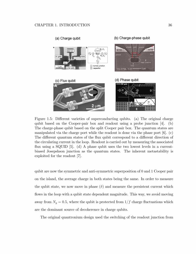
plement the quantum two level system. Fig. 1.5 shows SEM images of these di¤erent
types of qubits.
We have chosen the quantronium design as our qubit for the work described in
this thesis. The quantronium design uses a split Cooper pair box4 as shown in Fig.
1.6a. In this circuit, there are two small junctions with Josephson energy EJ=2 and a
large readout junction with a Josephson energy ERJ � 50EJ , all in a superconducting
loop. There are two control parameters which controls the energy spectrum of the
quantronium�the gate charge Ng = CgU=2e, and the superconducting phase � across
the two junctions which can be set by a �ux (�m = �='0) through the loop or
by applying a current bias (�R = arcsin(I'0=ERJ )) to the readout junction. The
quantronium has a special property when biased at the so called "sweet spot" (Ng =
0:5; � = 0). At this bias point, the transition frequency between the �rst two qubit
states is stationary with respect to both control variables Ng and �, i.e., the system
becomes immune to charge and �ux noise to �rst order. The quantum states of the
4See chapter 4 and ref. [38] for more details about the quantronium circuit
CHAPTER 1. INTRODUCTION 36
Figure 1.5: Di¤erent varieties of superconducting qubits. (a) The original chargequbit based on the Cooper-pair box and readout using a probe junction [4]. (b)The charge-phase qubit based on the split Cooper pair box. The quantum states aremanipulated via the charge port while the readout is done via the phase port [6]. (c)The di¤erent quantum states of the �ux qubit correspond to a di¤erent direction ofthe circulating current in the loop. Readout is carried out by measuring the associated�ux using a SQUID [5]. (d) A phase qubit uses the two lowest levels in a current-biased Josepshson junction as the quantum states. The inherent metastability isexploited for the readout [7].
qubit are now the symmetric and anti-symmetric superposition of 0 and 1 Cooper pair
on the island, the average charge in both states being the same. In order to measure
the qubit state, we now move in phase (�) and measure the persistent current which
�ows in the loop with a qubit state dependent magnitude. This way, we avoid moving
away from Ng = 0:5, where the qubit is protected from 1=f charge �uctuations which
are the dominant source of decoherence in charge qubits.
The original quantronium design used the switching of the readout junction from
CHAPTER 1. INTRODUCTION 37
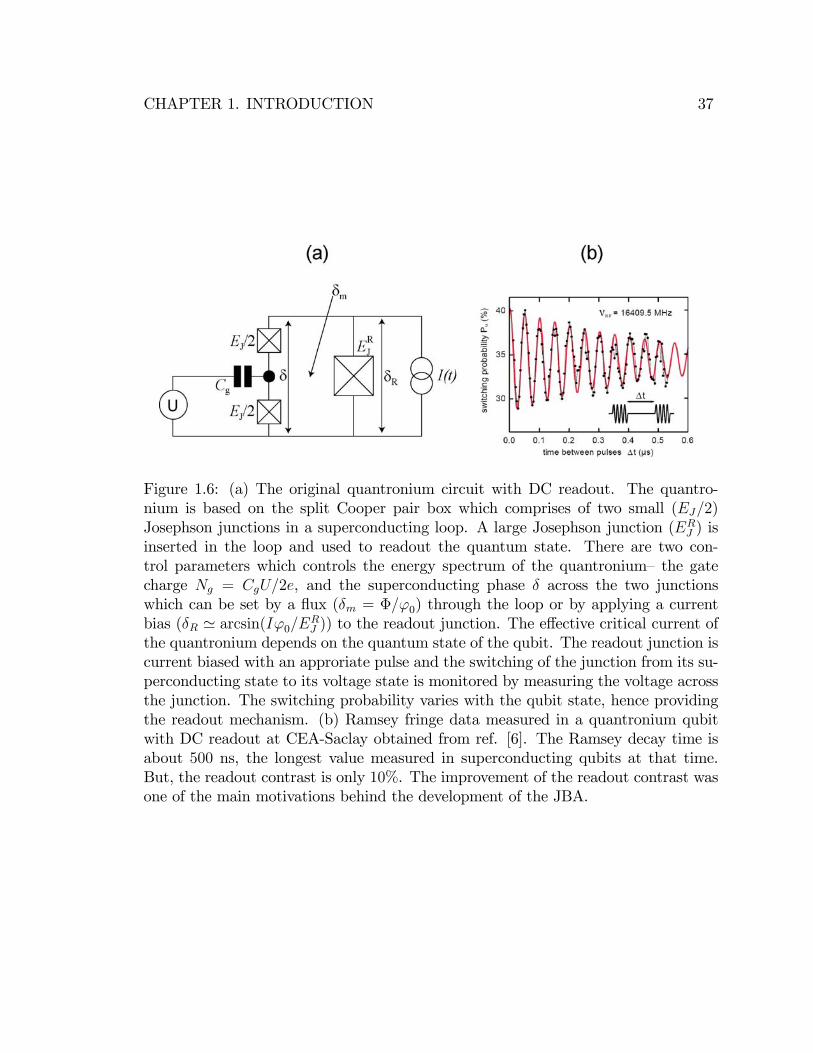
Figure 1.6: (a) The original quantronium circuit with DC readout. The quantro-nium is based on the split Cooper pair box which comprises of two small (EJ=2)Josephson junctions in a superconducting loop. A large Josephson junction (ERJ ) isinserted in the loop and used to readout the quantum state. There are two con-trol parameters which controls the energy spectrum of the quantronium�the gatecharge Ng = CgU=2e, and the superconducting phase � across the two junctionswhich can be set by a �ux (�m = �='0) through the loop or by applying a currentbias (�R ' arcsin(I'0=ERJ )) to the readout junction. The e¤ective critical current ofthe quantronium depends on the quantum state of the qubit. The readout junction iscurrent biased with an approriate pulse and the switching of the junction from its su-perconducting state to its voltage state is monitored by measuring the voltage acrossthe junction. The switching probability varies with the qubit state, hence providingthe readout mechanism. (b) Ramsey fringe data measured in a quantronium qubitwith DC readout at CEA-Saclay obtained from ref. [6]. The Ramsey decay time isabout 500 ns, the longest value measured in superconducting qubits at that time.But, the readout contrast is only 10%. The improvement of the readout contrast wasone of the main motivations behind the development of the JBA.

CHAPTER 1. INTRODUCTION 38
its superconducting state to the voltage state to discriminate between the qubit states.
In the absence of an external current bias, the system remains at the �magic�point
and one can carry out quantum manipulations by applying microwave pulses to the
gate port. The measurement process is initiated by passing a current through the big
junction, which in turn imposes a phase across the split Cooper pair box. The loop
currents thus generated, modify the amount of current �owing through the readout
junction. By carefully biasing the system with a current pulse of the right amplitude
and length, one can make the readout junction switch into its voltage state with high
probability when the qubit is in state j1i and very low probability when it is in state
j0i. This way one could discriminate between the two qubit states. Fig. 1.6b shows
the result of a Ramsey fringe experiment [6] yielding a coherence time T2 � 500ns.
At the start of this thesis work, this was the best result in the superconducting qubit
community and an important reason for choosing this system for our work. The
quantronium design also allows the separation between the read (phase) and write
(charge) ports which prevents complications due to cross-talk between the read and
write operation.
Nevertheless, there were still a few problems in the original design which needed
to be recti�ed in order to achieve better operation. A major issue was the generation
of quasi-particles when the readout junction switched into its voltage state. It is now
widely accepted that the presence of quasi-particles near the qubit is very harmful.
It leads to heating, poisoning of the qubit states and limits the repetition rate of
the experiment because one has to wait long enough to make sure that all the quasi-
particles have di¤used out (which can be quite long at the extremely low temperatures
at which the experiments are performed � 10 mK). Moreover, the recombination
CHAPTER 1. INTRODUCTION 39
process can itself produce excess noise for the adjacent circuitry[39]. The observed
contrast of Rabi oscillations and Ramsey fringes was also quite low (� 10%) [6] though
it was subsequently improved to about 40% using a clever combination of �ux and
current bias [40]. It was clear that a better readout was needed which would address
all these problems. This was the main motivation behind the development of the
Josephson Bifurcation Ampli�er.
Instead of probing the loop currents by biasing with a DC current and measuring
the probability of switching into the voltage state, we decided to bias the junction
with an AC current (microwaves) and probe the inductance of the quantronium.
The readout junction was shunted with a capacitor to form a non-linear oscillator
and energized with microwave pulses to bias it near a saddle-node bifurcation. The
qubit state modi�ed the bifurcation point of the non-linear oscillator which resulted
in the JBA ending up in either the low amplitude state or the high amplitude state
depending on whether qubit was in state j0i or j1i. Analogous to the previous
measurement scheme one can now measure the probability of switching from one
oscillation state to another to discriminate between the qubit states. This purely
dispersive method has the advantage of high speed and high �delity, with no on-
chip dissipation. This method avoids generation of quasi-particles since the readout
junction remains in the superconducting state at all times.
The next section brie�y summarizes the key results obtained in this thesis.
CHAPTER 1. INTRODUCTION 40
1.4 Summary of key results
1.4.1 JBA Measurements
The existence of a plasma like mode of oscillation in Josephson junctions was �rst
predicted by Josephson himself [3]. Several experiments followed which probed the
microwave power absorption at the plasma resonance [41, 42]. In our experiment, we
directly measure the plasma resonance in a coherent microwave re�ection experiment,
measuring both the magnitude and the phase of re�ected microwave signal. Typical
junction fabrication parameters limit the plasma frequency to the 20 - 100 GHz range
where techniques for addressing junction dynamics are inconvenient. We have chosen
to shunt the junction by a capacitive admittance to lower the plasma frequency by
more than an order of magnitude and attain a frequency in 1-2 GHz range (microwave
L-band). In this frequency range, a simple on-chip electrodynamic environment with
minimum parasitic elements can be implemented, and the hardware for precise signal
generation and processing is readily available. Since there is no intrinsic dissipation in
the oscillator in principle5, the phase of the re�ected signal contains all the information
about the resonance characteristics. The response of the system was studied in both
the linear and non-linear regime by varying the drive power and the result is shown
in Fig. 1.7.
The normalized re�ected signal phase as a function of drive frequency and power
is presented in the right panel of Fig. 1.7 as a two dimensional color plot. For
small excitation power, we recover the linear plasma resonance at 1:54GHz, shown
in yellow corresponding to � = 0. As the power is increased above �115 dBm, the
5In practice, the on-chip capacitive admittance always provides some dissipation but it is usuallyvery small.

CHAPTER 1. INTRODUCTION 41
Figure 1.7: Normalized re�ected signal phase � (wrap-around color scheme) as afunction of excitation frequency !d=2� and excitation power P . Experimental datais shown in the right panel. A vertical slice taken at !d=2� = 1:375 GHz (dashed linein the inset) shows the abrupt transition between two oscillation states of the system.The left panel is the result of numerical simulations of the full circuit including strayelements, and shows very good agreement with the experimental results.
plasma frequency decreases as expected for the non-linear oscillator. The boundary
between the leading-phase region (green) and the lagging-phase region (red) therefore
curves for high powers. When we increase the drive power at a constant frequency
slightly below the plasma frequency, the phase as a function of power undergoes an
abrupt step (dashed line), as predicted. This represents the transition from the low
amplitude state to the high amplitude state. For yet greater powers (> �90 dBm),
we encounter a new dynamical regime (black region in Fig. 1.7) where � appears to
di¤use between the wells of the cosine potential. This was con�rmed by the presence
of an unambiguous audio frequency AC resistance in the black region (see section
3.4). In the inset of right panel of Fig. 1.7, we illustrate the sequence of dynamical
transitions by plotting � as a function of incident power at !d=2� = 1:375GHz. For

CHAPTER 1. INTRODUCTION 42
P < �102 dBm, the phase is independent of power (� oscillates in a single well in the
harmonic-like, phase-leading state, letter A). For �102 dBm < P < �90 dBm, the
phase evolves with power and � still remains within the same well, but oscillates in
the anharmonic phase-lagging state (letter B). Finally, for P > �90 dBm, the average
phase of the re�ected signal saturates to -180 degrees, corresponding to a capacitive
short circuit. This last value is expected if � hops randomly between wells, the e¤ect
of which is to neutralize the Josephson inductive admittance.
The above measurements were taken using a network analyzer which only allows
for slow frequency sweeps. In other measurements (see Chapter 3), where the power is
ramped in less than 100 ns, we veri�ed that the transition between dynamical states
is hysteretic, another prediction of the theory. To explain the complete frequency
and power dependence of the transitions shown in the right panel of Fig. 1.7, we
have performed numerical simulations by solving the full circuit model (equation
1.5 + stray elements). The result of this calculation is shown in the left panel of
Fig. 1.7. It correctly predicts the variation of the plasma frequency with excitation
power, and the boundaries of the phase di¤usion region. The agreement between
theory and experiment is remarkable in view of the simplicity of the model which
uses only measured parameters, and only small di¤erences in the exact shape of
region boundaries are observed.
1.4.2 Qubit measurements
As discussed in section 1.2, the transition from the low amplitude state to the high
amplitude state of the JBA depends sensitively on the critical current of the junction.
This is exploited to make a readout for superconducting qubits using the JBA. The
CHAPTER 1. INTRODUCTION 43
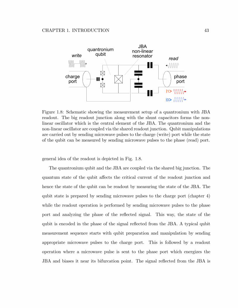
Figure 1.8: Schematic showing the measurement setup of a quantronium with JBAreadout. The big readout junction along with the shunt capacitors forms the non-linear oscillator which is the central element of the JBA. The quantronium and thenon-linear oscillator are coupled via the shared readout junction. Qubit manipulationsare carried out by sending microwave pulses to the charge (write) port while the stateof the qubit can be measured by sending microwave pulses to the phase (read) port.
general idea of the readout is depicted in Fig. 1.8.
The quantronium qubit and the JBA are coupled via the shared big junction. The
quantum state of the qubit a¤ects the critical current of the readout junction and
hence the state of the qubit can be readout by measuring the state of the JBA. The
qubit state is prepared by sending microwave pulses to the charge port (chapter 4)
while the readout operation is performed by sending microwave pulses to the phase
port and analyzing the phase of the re�ected signal. This way, the state of the
qubit is encoded in the phase of the signal re�ected from the JBA. A typical qubit
measurement sequence starts with qubit preparation and manipulation by sending
appropriate microwave pulses to the charge port. This is followed by a readout
operation where a microwave pulse is sent to the phase port which energizes the
JBA and biases it near its bifurcation point. The signal re�ected from the JBA is
CHAPTER 1. INTRODUCTION 44
then analyzed to determine whether the JBA is in the low amplitude state or the high
amplitude state. The process is then repeated thousands of times and the probability
of switching from the low amplitude to the high amplitude state is determined (output
signal). The measurement is arranged so that the switching probability is close to
zero when the qubit is in its ground state while the switching probability is close to
one when the qubit is in its �rst excited state. Ideally, we would like the switching
probability to be zero for qubit ground state and one for qubit excited state. The
optimization of the qubit readout performance is discussed in chapter 6.
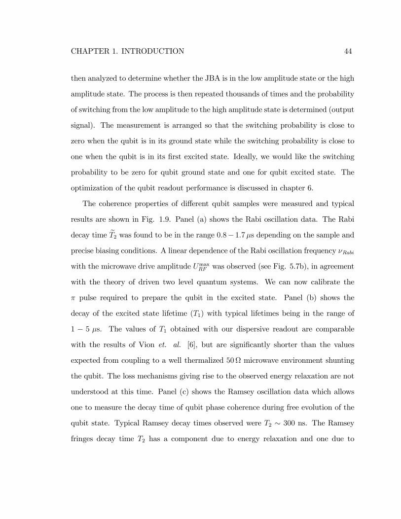
The coherence properties of di¤erent qubit samples were measured and typical
results are shown in Fig. 1.9. Panel (a) shows the Rabi oscillation data. The Rabi
decay time eT2 was found to be in the range 0:8� 1:7�s depending on the sample andprecise biasing conditions. A linear dependence of the Rabi oscillation frequency �Rabi
with the microwave drive amplitude UmaxRF was observed (see Fig. 5.7b), in agreement
with the theory of driven two level quantum systems. We can now calibrate the
� pulse required to prepare the qubit in the excited state. Panel (b) shows the
decay of the excited state lifetime (T1) with typical lifetimes being in the range of
1 � 5 �s. The values of T1 obtained with our dispersive readout are comparable
with the results of Vion et. al. [6], but are signi�cantly shorter than the values
expected from coupling to a well thermalized 50 microwave environment shunting
the qubit. The loss mechanisms giving rise to the observed energy relaxation are not
understood at this time. Panel (c) shows the Ramsey oscillation data which allows
one to measure the decay time of qubit phase coherence during free evolution of the
qubit state. Typical Ramsey decay times observed were T2 � 300 ns. The Ramsey
fringes decay time T2 has a component due to energy relaxation and one due to
CHAPTER 1. INTRODUCTION 45
Figure 1.9: Summary of qubit coherence measurement. (a)Rabi oscillations of theswitching probability as a function of the duration � of a square pulse applied on thegate. Solid green curve is an exponentially decaying sinusoidal �t with eT2 = 1:6�s.(b) Decay of the excited state switching probability after preparing the qubit inthe excited state by a � pulse, as a function of the waiting time tw between thepreparation pulse and the readout pulse. Solid green curve is an exponential �t witha decay constant T1 = 3.2�s. The dashed line indicates the value of Pswitch in theabsense of a � pulse. (c) Ramsey fringes obtained with two �=2 pulses separated bythe time interval �t. The pulse frequency was detuned from the Larmor frequency by20MHz. The green curve is a exponentially decaying sinusoid �t. The decay time T2is 320ns. (d) Switching probability as a function of maximum drive current and qubitstate. The vertical dotted line represents value of drive current at which maximaldi¤erence in Pswitch is observed. The solid line connects the observed data points inthe j0i state and the dashed line is a copy of the solid line horizontally shifted tooverlap the j1i state data at low values of Pswitch.
CHAPTER 1. INTRODUCTION 46
pure dephasing: 1=T2 = 1= (2T1) + 1=T', where T' represents pure dephasing. In our
measurements, T2 is usually dominated by pure dephasing which is due to �uctuations
in the qubit transition frequency originating from 1=f o¤set charge noise. Recent
qubit measurements using the cavity version of the JBA show that the dephasing
times are compatible with the magnitude of the typical 1=f o¤set noise seen in these
systems [43]. Immunity to 1=f charge noise can be achieved by increasing the EJ=EC
ratio in these qubits and we observed some improvement in the pure dephasing time
for such samples (see chapter 5). This strategy is now being implemented in some
new qubit implementations which use very large EJ=EC ratios to almost eliminate
the gate charge dependence of the transition frequency [44, 45].
Panel (d) shows the S-curves corresponding to the qubit being in the ground and
excited state. The open circle points in blue and red correspond to data for the
qubit ground and excited states respectively while the solid black line is the best �t
through the ground state data. The dashed black line is the same as the solid black
line but shifted to match the excited state data for low switching probabilities. This
was done to indicate the small di¤erence in the shape of the excited state S-curve
resulting in the reduction of readout contrast. The observed contrast for this data is
about 15� 30% smaller than expected. In a set of experiments described in chapter
6, we used two readout pulses in succession to determine that a 15 � 30% loss of
qubit population occurs, even before the resonator is energized to its operating point.
We attribute this loss to spurious on-chip defects [46]. As photons are injected into
the resonator, the e¤ective qubit frequency is lowered due to a Stark shift via the
phase port [47]. When the Stark shifted frequency coincides with the frequency of
an on-chip defect, a relaxation of the qubit can occur. Typically, the qubit frequency
CHAPTER 1. INTRODUCTION 47
spans 200 � 300MHz before the state of the qubit is registered by the readout, and
3 � 4 spurious resonances are encountered in this range. Chapter 6 discusses these
issues in more detail.
1.4.3 Escape measurements in the quantum regime
The ultimate sensitivity of the JBA depends on the e¤ective intensity of �uctuations
felt by it at the operating temperature (chapter 2). As the operating temperature
approaches zero, quantum �uctuations start becoming important. In the classical
regime, the transitions are governed by some kind of activation process and ther-
mal noise activates the system over an e¤ective barrier [27]. But what mechanism
governs the transition as T ! 0 ? More importantly, what sets the classical to quan-
tum crossover temperature? Borrowing ideas from the theory of macroscopic quan-
tum tunnelling (MQT) in current biased Josephson junctions (see [48] and references
therein), we can make an educated guess that the crossover temperature must be
related to the plasma frequency of the oscillator. It turns out that for this driven,
non-linear system, the transition between the metastable states is predominantly due
to an activation process even as T ! 0[49, 50, 51], but the origin of �uctuations is
the zero-point �uctuations of the oscillator. There has also been some recent work on
the signatures of quantum behavior in driven non-linear systems and its dependence
on system parameters[52].
The escape in the quantum regime is closely connected to the Dynamical Casimir
E¤ect (DCE)� an elusively weak phenomenon predicted about 40 years ago [53, 54]
but whose theory remains essentially experimentally unveri�ed. In perhaps the most
promising opto-mechanical realization of the DCE [55], one of the mirrors of a Fabry-
CHAPTER 1. INTRODUCTION 48
Perot cavity is driven by a force that periodically varies the cavity�s geometric length
at a frequency which is a multiple of the lowest cavity mode frequency !0. Ac-
cording to prediction, even when the cavity is at a low temperature T such that it is
initially void of all real electromagnetic radiation (~!0 >> kBT ) and contains only
virtual zero-point quantum �uctuations, the mirror motion should spontaneously cre-
ate thermal radiation inside the cavity. Our experiment implements a fully electrical
version of the DCE where we have periodically varied the frequency of an electromag-
netic resonator not by mechanical means, but through an element whose reactance
can be modulated by an electrical signal. This element is the Josephson tunnel junc-
tion in the JBA which can be modelled as an inductor which is both non-linear and
purely dispersive. The non-linearity enables electrical modulation of the resonator
inductance while the absence of dissipation eliminates parasitic channels of heat pro-
duction.
Our implementation can be classi�ed as a pumped, doubly degenerate parametric
resonator operating in the quantum regime. Its operation can be described as the
parametric conversion of positive frequency components at the idler and signal fre-
quencies into their negative counterparts. Josephson parametric ampli�ers[9] which
essentially perform the same function are also potential candidates for observing the
DCE, but a major experimental challenge is to detect the small e¤ective temperature
of the output photon �eld produced by the DCE, and requires a detector with mini-
mal coupling loss and quantum-noise limited sensitivity. In our experiment, we use a
unique approach by operating the non-linear resonator close to a saddle-node bifur-
cation which can then also function as a detector. Thermal noise that, according to
the DCE, should be generated from the ampli�cation of quantum �uctuations inside
CHAPTER 1. INTRODUCTION 49
the resonator, here provokes the switching of the system from the initially prepared
low amplitude state into the high amplitude state. By performing a calibration in
the high temperature regime where the switching process is dominated solely by ordi-
nary black-body thermal radiation, we can infer the temperature of the spontaneously
created noise in the quantum regime and compare it to theory.
The theory of quantum escape [49, 50, 51] predicts6 that the e¤ective temperature
is given by
Teff (T ) =~!d2kB
coth
�~!d2kBT
�(1.7)
From the above equation, we can see that in the classical regime (kBT � ~!d), the
e¤ective temperature Teff tends to the physical temperature T . On the other hand,
as T ! 0, Teff ! ~!d=2kB. We note that this result is di¤erent from the MQT
results where the saturation temperature is given by ~!d=7:2kB [48]. This is due to
the fact the escape from the metastable state in the JBA takes place via quantum
activation and not via tunneling.
The experimental procedure is similar to the MQT experiment [48]. We bias the
JBA near the bifurcation point and monitor the rate of escape as a function of the
distance to the bifurcation point. Since we know this expected dependence from
theory [27], we can infer the e¤ective escape temperature. This experiment is then
repeated for di¤erent temperatures and the corresponding escape temperatures are
recorded (see chapter 8 and [56]). Since we expect the escape temperature to be equal
to the physical temperature in the classical regime, we normalize the data so that
the measured escape temperature matches the physical temperature in the classical
regime. This can only be done if we are sure that the only source of �uctuations
6This result is derived in Chapter 7 using a di¤erent approach based on Input-Output theory.
CHAPTER 1. INTRODUCTION 50
felt by the system in the classical regime is the thermal noise corresponding to that
temperature. In order to verify this, we also measured at every temperature point, the
escape from the DC current biased junction which provides an independent calibration
of the noise intensity in the system. We then observe how the escape temperature
in the RF case varies as the physical temperature is lowered. The experiment was
performed on two samples with di¤erent plasma frequency and the result is shown in
Fig. 1.10.
The blue square points correspond to the sample with the !p=2� = 1:67 GHz while
the red circles correspond to the sample with !p=2� = 4:69 GHz. The corresponding
drive frequencies are !d=2� = 1:525 GHz and !d=2� = 4:450 GHz. The solid colored
lines are a plot of equation 1.7 as a function of physical temperature for the corre-
sponding values of drive frequency. We note that the solid lines �t the data quite
well. The dashed black line represents the equation Tesc = T for comparison. In the
inset, we show the data for the escape temperature inferred from DC switching mea-
surements and the DC saturation temperatures are indicated with colored arrows on
the main plot. For our system parameters, we should have measured TMQTeff = T over
the entire temperature range. We believe that the small residual deviations are due
to improperly thermalized �lters and noise in the dual biasing con�guration. Another
possibility is the contribution of higher frequency plasma dynamics due to residual
inductance in series with the shunting capacitor. Nevertheless, we note that the data
for escape in the quantum regime agrees well with the theoretical predictions and the
saturation temperatures corresponds to ~!d=2kB. This experiment provides evidence
for the existence of the electrical version of DCE at microwave frequencies involving a
Josephson junction RF driven near its dynamic bifurcation point. From the point of

CHAPTER 1. INTRODUCTION 51
Figure 1.10: Escape temperature v.s. bath temperature for an RF driven Joseph-son oscillator biased near a bifurcation point. The escape temperature is inferredby monitoring the transition rates from the low amplitude to the high amplitudestate of the Josephson oscillator. The blue square points correspond to the samplewith the !p=2� = 1:67 GHz while the red circles correspond to the sample with!p=2� = 4:69 GHz. The corresponding drive frequencies are !d=2� = 1:525 GHz and!d=2� = 4:450 GHz. The solid colored lines are a plot of equation 1.7 as a functionof physical temperature for the corresponding values of !d. We note that solid lines�t the data quite well. The dashed black line represents the equation Tesc = T forcomparison. The errors in the measurement of escape temperature are set by theamount of statistics obtained and the stability of the drive power. It is usually lessthan 5%. In the inset, we show the data for the escape temperature inferred fromDC switching measurements and the DC saturation temperatures are indicated withcolored arrows on main plot.
CHAPTER 1. INTRODUCTION 52
view of signals coming from the load impedance, the RF biased junction behaves as a
parametric ampli�er and, in the quantum regime, converts quantum �uctuations into
thermal noise. In other experiments described in chapter 8, we have characterized
the performance of the JBA as a parametric ampli�er for amplifying small signals
coupled via the drive port. Data indicates that performance near the quantum limit
is possible.
1.5 Thesis overview
Quantum measurements of solid-state systems, such as the readout of superconduct-
ing quantum bits challenge conventional low-noise ampli�cation techniques. Ideally,
the ampli�er for a quantum measurement should minimally perturb the measured
system while maintaining su¢ cient sensitivity to overcome the noise of subsequent
elements in the ampli�cation chain. Additionally, the drift of materials properties
in solid-state systems mandates a fast acquisition rate to permit measurements in
rapid succession. In this thesis, we harness the sensitivity of a dynamical system -
a non-linear oscillator tuned near a bifurcation point to meet these requirements. In
this new scheme, all available degrees of freedom in the dynamical system participate
in information transfer and none contribute to unnecessary dissipation resulting in
excess noise. We have used a superconducting tunnel junction which can be viewed
as a non-linear inductor to construct our non-linear oscillator. The superconduct-
ing tunnel junction is the only electronic circuit element which remains non-linear
and non-dissipative at arbitrary low temperatures. As the key component of present
superconducting ampli�ers, it is known to exhibit a high degree of stability.
We have performed a novel, phase-sensitive, microwave experiment demonstrat-

CHAPTER 1. INTRODUCTION 53
ing that the Josephson plasma oscillation can transition between the two dynamical
states predicted for a driven non-linear system[28]. Using di¤erent samples, we have
shown that this dynamical phenomenon is stable, reproducible and can be precisely
controlled, thus opening the possibility for practical applications like ampli�cation
which we call the Josephson Bifurcation Ampli�er. A signal coupled to the critical
current of the junction can be detected by monitoring the changes in the dynamical
state of the non-linear oscillator[57]. This approach was used to develop a non-linear,
dispersive readout for superconducting qubits by coupling a Cooper-pair box with
the JBA[29]. In order to perform a readout, the resonator is RF-energized to a level
where its oscillation state now acts as a sensitive pointer of the qubit state. This tech-
nique does not generate any dissipation on chip since the resonator is only damped
by circuitry outside the chip, i.e., a 50 transmission line with a matched circulator
and ampli�er, and enables a high-�delity qubit readout with a MHz repetition rate.
We have measured Rabi oscillations and Ramsey fringes with su¢ cient speed that
real time �ltering to correct for drifts in the charge and �ux bias becomes possible.
Also, several successive readouts may be performed within the energy relaxation time
of the qubit (T1). This gives valuable information on the readout-induced interaction
between the qubit and its environment, and accounts for the observed contrast. The
JBA was also used as a parametric ampli�er to amplify small signals coupled via the
drive port (as opposed to parametric coupling of signals in the qubit readout) achiev-
ing signal gain of about 20 dB and near quantum limited noise temperature. The
parametric ampli�er model of the JBA also helps us understand its behavior in the
quantum regime. The dynamical transition between the metastable states of the JBA
takes place via an activation process even in the limit T ! 0 as opposed to a tunnel-
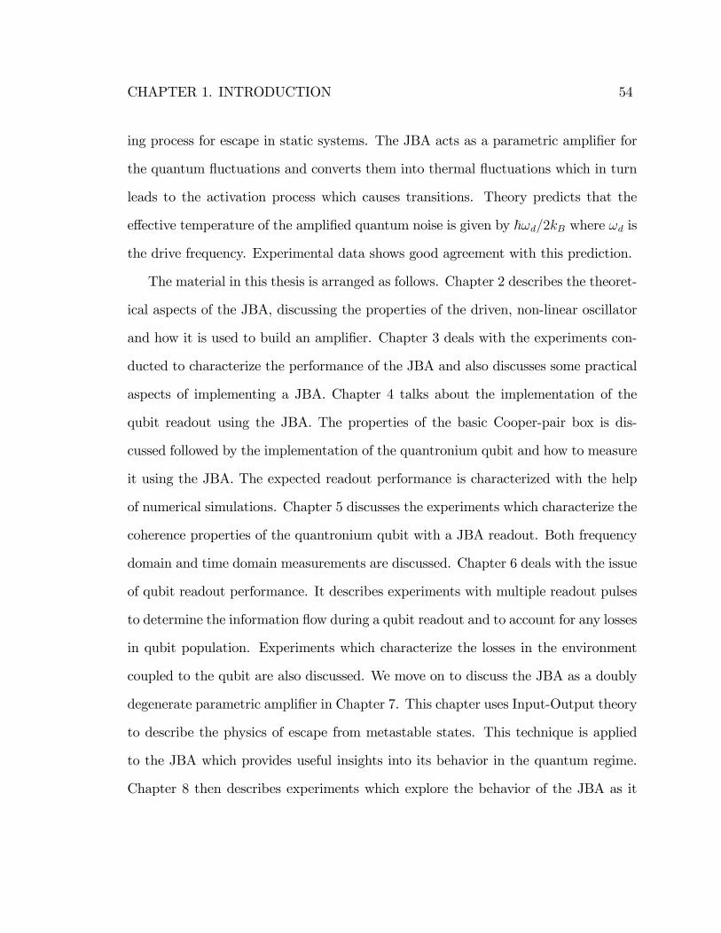
CHAPTER 1. INTRODUCTION 54
ing process for escape in static systems. The JBA acts as a parametric ampli�er for
the quantum �uctuations and converts them into thermal �uctuations which in turn
leads to the activation process which causes transitions. Theory predicts that the
e¤ective temperature of the ampli�ed quantum noise is given by ~!d=2kB where !d is
the drive frequency. Experimental data shows good agreement with this prediction.
The material in this thesis is arranged as follows. Chapter 2 describes the theoret-
ical aspects of the JBA, discussing the properties of the driven, non-linear oscillator
and how it is used to build an ampli�er. Chapter 3 deals with the experiments con-
ducted to characterize the performance of the JBA and also discusses some practical
aspects of implementing a JBA. Chapter 4 talks about the implementation of the
qubit readout using the JBA. The properties of the basic Cooper-pair box is dis-
cussed followed by the implementation of the quantronium qubit and how to measure
it using the JBA. The expected readout performance is characterized with the help
of numerical simulations. Chapter 5 discusses the experiments which characterize the
coherence properties of the quantronium qubit with a JBA readout. Both frequency
domain and time domain measurements are discussed. Chapter 6 deals with the issue
of qubit readout performance. It describes experiments with multiple readout pulses
to determine the information �ow during a qubit readout and to account for any losses
in qubit population. Experiments which characterize the losses in the environment
coupled to the qubit are also discussed. We move on to discuss the JBA as a doubly
degenerate parametric ampli�er in Chapter 7. This chapter uses Input-Output theory
to describe the physics of escape from metastable states. This technique is applied
to the JBA which provides useful insights into its behavior in the quantum regime.
Chapter 8 then describes experiments which explore the behavior of the JBA as it
CHAPTER 1. INTRODUCTION 55
goes from the classical to the quantum regime. In particular, measurements of the
transition rates from the low amplitude to the high amplitude states as a function of
temperature, are described. Data describing the performance of the JBA as a para-
metric ampli�er are also presented. Finally, we provide some directions for future
experiments in chapter 9 and conclusions of this thesis in chapter 10.
Chapter 2
Josephson Bifurcation Ampli�er: Theory
In this chapter we will introduce the Josephson Bifurcation Ampli�er (JBA), the main
subject of research in this thesis. We will begin by describing a driven, non-linear
oscillator and its properties. We will then describe how one can use such a system to
make a sensitive detector/ampli�er. Finally, we will discuss the various properties of
the JBA and derive formulae to compute its performance.
2.1 General properties of a driven non-linear oscillator
Periodically driven non-linear oscillators often have several stable states, that cor-
respond to steady state oscillations di¤ering in their amplitude and phase. A well
known example of a non-linear oscillator is a simple pendulum(Fig. 2.1 (a)).
In a linear oscillator, the restoring force is proportional to the displacement. But
the restoring force in a pendulum is proportional to the sine of the angle �v with
respect to the vertical, which makes it non-linear. In other words, the frequency of
oscillations depends on its amplitude or energy. As the oscillation energy increases,
56
CHAPTER 2. JOSEPHSON BIFURCATION AMPLIFIER: THEORY 57
Figure 2.1: a) Simple pendulum as a non-linear oscillator. The restoring force isproportional to the sine of the angular displacement which is the origin of the non-linearity. The frequency for small oscillations is given by (g=l)1=2. b) A plot of thenormalized angular frequency (!0= (g=l)
1=2) as a function of the normalized oscilla-tion energy of the pendulum. �maxv now refers to the amplitude of oscillation. Theenergy of oscillation is given by the potential energy at maximum displacement i.e.mgl (1� cos �maxv ) with the maximum value mgl at �maxv = �. We note how thefrequency �rst decreases linearly with energy. The slope at the origin is �1=4 asindicated by the dashed line. The green line is the expected behavior for a linearoscillator. We have assumed that there is no damping in the pendulum
the frequency of oscillation decreases (sin �maxv � �maxv ). This behavior is illustrated
in Fig. 2.1(b). The frequency of small oscillations (sin �v ' �v) is given by !0 =pg=l, where g is the acceleration due to gravity and l is the length of the pendulum.
Now consider the situation where the pendulum is subject to periodic driving at a
frequency !d < !0. If the pendulum has �nite damping, this driving frequency has
to satisfy1 !0 � !d >p3� where � is the amplitude damping coe¢ cient. For a
large enough strength of driving, the pendulum can respond in two di¤erent ways
[58]. It can either respond by oscillating with a small amplitude at frequency !d
where its natural frequency (� !0) is di¤erent than the driving frequency. This is the
1This condition is derived in the next section
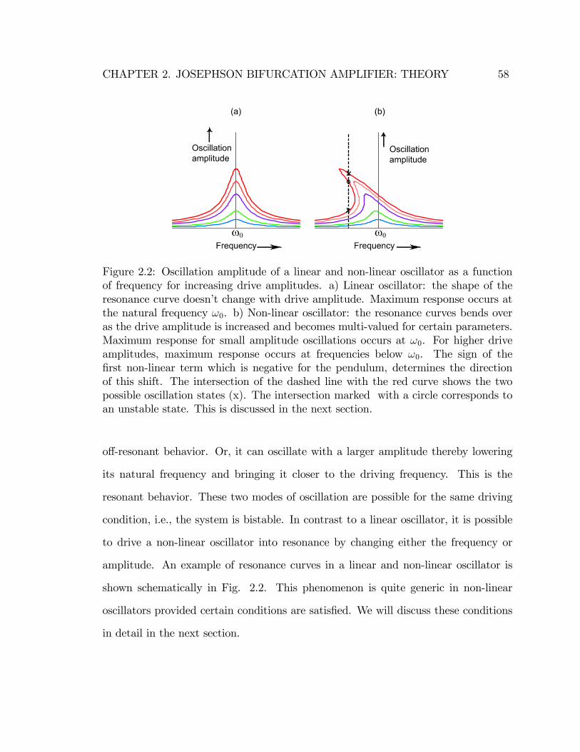
CHAPTER 2. JOSEPHSON BIFURCATION AMPLIFIER: THEORY 58
Figure 2.2: Oscillation amplitude of a linear and non-linear oscillator as a functionof frequency for increasing drive amplitudes. a) Linear oscillator: the shape of theresonance curve doesn�t change with drive amplitude. Maximum response occurs atthe natural frequency !0. b) Non-linear oscillator: the resonance curves bends overas the drive amplitude is increased and becomes multi-valued for certain parameters.Maximum response for small amplitude oscillations occurs at !0. For higher driveamplitudes, maximum response occurs at frequencies below !0. The sign of the�rst non-linear term which is negative for the pendulum, determines the directionof this shift. The intersection of the dashed line with the red curve shows the twopossible oscillation states (x). The intersection marked with a circle corresponds toan unstable state. This is discussed in the next section.
o¤-resonant behavior. Or, it can oscillate with a larger amplitude thereby lowering
its natural frequency and bringing it closer to the driving frequency. This is the
resonant behavior. These two modes of oscillation are possible for the same driving
condition, i.e., the system is bistable. In contrast to a linear oscillator, it is possible
to drive a non-linear oscillator into resonance by changing either the frequency or
amplitude. An example of resonance curves in a linear and non-linear oscillator is
shown schematically in Fig. 2.2. This phenomenon is quite generic in non-linear
oscillators provided certain conditions are satis�ed. We will discuss these conditions
in detail in the next section.
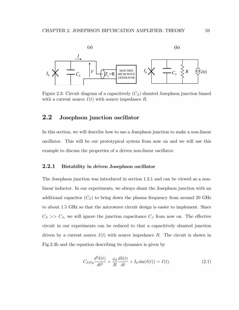
CHAPTER 2. JOSEPHSON BIFURCATION AMPLIFIER: THEORY 59
Figure 2.3: Circuit diagram of a capacitively (CS) shunted Josephson junction biasedwith a current source I(t) with source impedance R.
2.2 Josephson junction oscillator
In this section, we will describe how to use a Josephson junction to make a non-linear
oscillator. This will be our prototypical system from now on and we will use this
example to discuss the properties of a driven non-linear oscillator.
2.2.1 Bistability in driven Josephson oscillator
The Josephson junction was introduced in section 1.2.1 and can be viewed as a non-
linear inductor. In our experiments, we always shunt the Josephson junction with an
additional capacitor (CS) to bring down the plasma frequency from around 20 GHz
to about 1:5 GHz so that the microwave circuit design is easier to implement. Since
CS >> CJ , we will ignore the junction capacitance CJ from now on. The e¤ective
circuit in our experiments can be reduced to that a capacitively shunted junction
driven by a current source I(t) with source impedance R. The circuit is shown in
Fig.2.3b and the equation describing its dynamics is given by
CS'0d2�(t)
dt2+'0R
d�(t)
dt+ I0 sin(�(t)) = I(t): (2.1)
CHAPTER 2. JOSEPHSON BIFURCATION AMPLIFIER: THEORY 60
Note that the above equation is identical to the well known RCSJ equation (resistively
and capacitively shunted junction). The resistance R is often used in literature to
describe the quasi-particle resistance of the junction. It is also used to describe a
shunt resistance whose function is to damp the plasma oscillations of the junction.
This is not the case here. In our experiments, we use microwave signals, propagating
on a transmission line to bias the Josephson oscillator (Fig.2.3a). Here, the resistance
R describes the characteristic impedance (which is real) of the transmission line or
equivalently, the source impedance of the matched, microwave signal generator. At
microwave frequencies, there are no ideal current or voltage sources and they usually
have a �nite source impedance R = 50 . We have chosen to represent the microwave
source as an ideal current source shunted with a resistance R. Since we always work
with the junction in its superconducting state, the Josephson oscillator has no intrinsic
dissipation2. Dissipation enters equation 2.1 only due to the fact that the oscillator is
connected to a transmission line which provides a mechanism for energy to leak out
of the oscillator. See section 7.1 for a more detailed discussion of these ideas.
In equation 2.1, the non-linear term is given by the sine of the phase di¤erence
across the junction - just like in the pendulum. Similarly, the frequency of natural
oscillations decreases with increasing amplitude. We will now derive the condition
for bistability when this non-linear oscillator is subject to harmonic driving, i.e.,
I(t) = IRF cos(!dt). Rewriting the above equation for a harmonic drive at frequency
!d, and retaining only the �rst non-linear term in the expansion of the sine term, we
2This is true provided the operating temperature (� 10 mK) is much lower than the criticaltemperature of the superconductor (� 1 K). Also the frequencies used (� 1 GHz) are much belowthe gap frequency (� 100 GHz) of the superconductor.
CHAPTER 2. JOSEPHSON BIFURCATION AMPLIFIER: THEORY 61
get:d2�(t)
dt2+ 2�
d�(t)
dt+ !2p
��(t)� �(t)
3
6
�= !2p
IRFI0cos(!dt) (2.2)
where � = 1=2RCS is the damping rate of the oscillation amplitude and !p =pI0= ('0CS) is the plasma frequency. We expect that the oscillator will respond
predominantly at the frequency of driving (!d). Therefore, it is convenient to de-
scribe the dynamics by using dimensionless, slow complex amplitudes [27] as below:
�(t) =
s2!d�!
3 (u(�) exp (i!dt) + u
�(�) exp (�i!dt)) (2.3)
where
= !2p=6 (2.4)
is the magnitude of the coe¢ cient of the non-linear term (_ � (t)3),
�! = !p � !d (2.5)
is the detuning of the drive from the plasma frequency, and
� = �!t (2.6)
is the new dimensionless, slow time variable. Substituting 2.3 into 2.2, we get:
�!
!d
d2u
d� 2+ (2�
!d+ 2i)
du
d�+
�2
�!2p � !2d2!d�!
�+i2�
�!� 2 juj2
�u(�) = 2
p� (2.7)

CHAPTER 2. JOSEPHSON BIFURCATION AMPLIFIER: THEORY 62
where
� =3 !4pI
2RF
32I20!3d(�!)
3(2.8)
is the reduced drive strength. We will now make some approximations. We only
consider under-damped oscillators, i.e., 2�=!p << 1. Also !d � !p, i.e., �!=!d <<
1. Making these approximations, equation 2.7 reduces to
du
d�= � u
� iu
�juj2 � 1
�� ip� (2.9)
where
= j�!j =� (2.10)
is the reduced detuning.
In order to �nd the steady state solutions, we set du=d� = 0 and we get a complex
algebraic equation
� u
� u
�juj2 � 1
�= ip� (2.11)
Multiplying equation 2.11 by its complex conjugate, we get a cubic equation for the
modulus square of the complex amplitude juj2:
juj2
2+ juj2
�juj2 � 1
�2= � (2.12)
Provided >p3, the above equation has three real roots for a certain range of �.
The extreme points of this range are called the bifurcation points and are given by
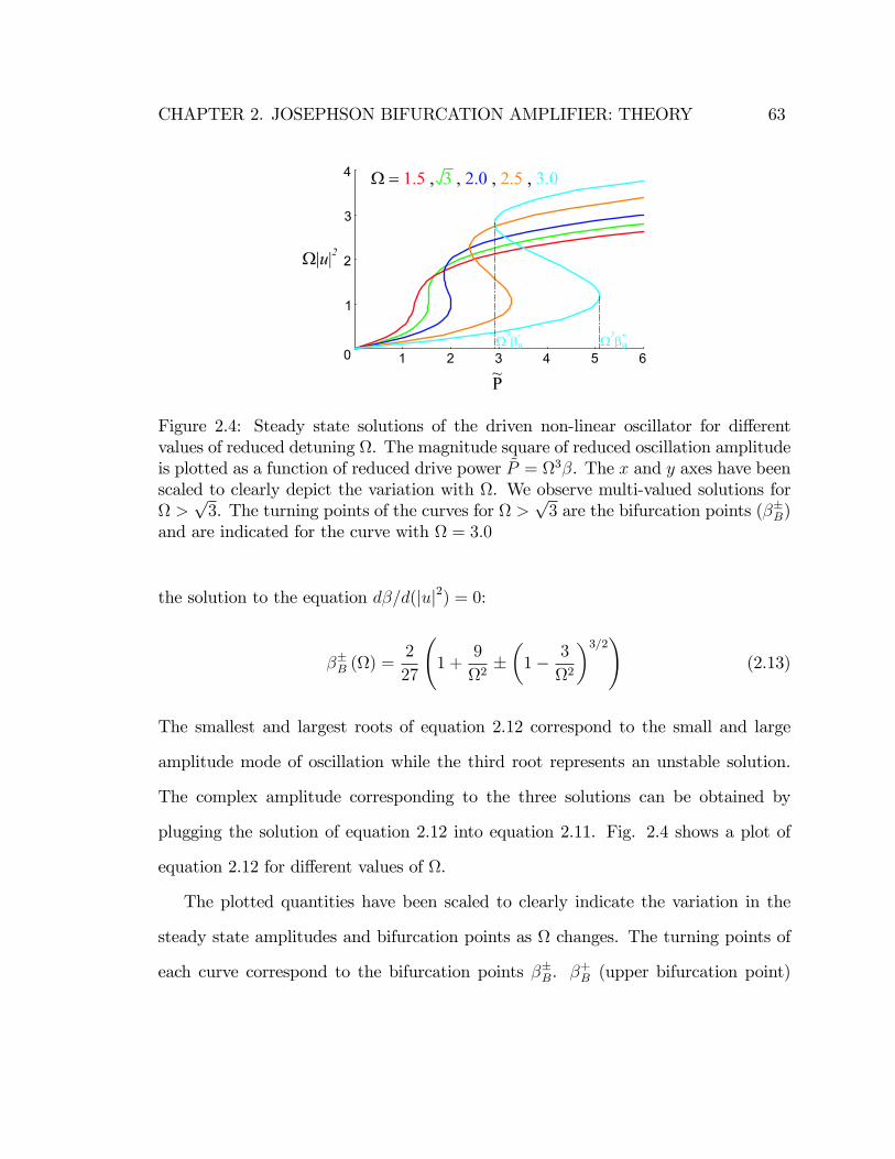
CHAPTER 2. JOSEPHSON BIFURCATION AMPLIFIER: THEORY 63
Figure 2.4: Steady state solutions of the driven non-linear oscillator for di¤erentvalues of reduced detuning . The magnitude square of reduced oscillation amplitudeis plotted as a function of reduced drive power ~P = 3�. The x and y axes have beenscaled to clearly depict the variation with . We observe multi-valued solutions for >
p3. The turning points of the curves for >
p3 are the bifurcation points (��B)
and are indicated for the curve with = 3:0
the solution to the equation d�=d(juj2) = 0:
��B () =2
27
1 +
9
2��1� 3
2
�3=2!(2.13)
The smallest and largest roots of equation 2.12 correspond to the small and large
amplitude mode of oscillation while the third root represents an unstable solution.
The complex amplitude corresponding to the three solutions can be obtained by
plugging the solution of equation 2.12 into equation 2.11. Fig. 2.4 shows a plot of
equation 2.12 for di¤erent values of .
The plotted quantities have been scaled to clearly indicate the variation in the
steady state amplitudes and bifurcation points as changes. The turning points of
each curve correspond to the bifurcation points ��B. �+B (upper bifurcation point)
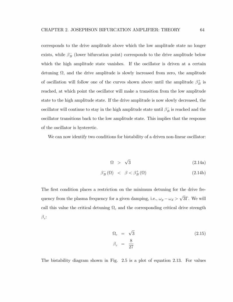
CHAPTER 2. JOSEPHSON BIFURCATION AMPLIFIER: THEORY 64
corresponds to the drive amplitude above which the low amplitude state no longer
exists, while ��B (lower bifurcation point) corresponds to the drive amplitude below
which the high amplitude state vanishes. If the oscillator is driven at a certain
detuning , and the drive amplitude is slowly increased from zero, the amplitude
of oscillation will follow one of the curves shown above until the amplitude �+B is
reached, at which point the oscillator will make a transition from the low amplitude
state to the high amplitude state. If the drive amplitude is now slowly decreased, the
oscillator will continue to stay in the high amplitude state until ��B is reached and the
oscillator transitions back to the low amplitude state. This implies that the response
of the oscillator is hysteretic.
We can now identify two conditions for bistability of a driven non-linear oscillator:
>p3 (2.14a)
��B () < � < �+B () (2.14b)
The �rst condition places a restriction on the minimum detuning for the drive fre-
quency from the plasma frequency for a given damping, i.e., !p�!d >p3�. We will
call this value the critical detuning c and the corresponding critical drive strength
�c:
c =p3 (2.15)
�c =8
27
The bistability diagram shown in Fig. 2.5 is a plot of equation 2.13. For values
CHAPTER 2. JOSEPHSON BIFURCATION AMPLIFIER: THEORY 65
Figure 2.5: Bistability diagram in the plane of reduced drive power ( ~P= ~Pc =(3��B)=(
3c�
�c )) and detuning (). The power is plotted on log units to enable
easy comparison with experimental plots. The x-axis has been plotted as a negativequantity to emphasize that for the Josephson oscillator, we need !d � !p < 0 toobserve bistability. The red and blue curves represent the upper (�+B) and lower (�
�B)
bifurcation points as a function of for >p3. The area between these two curves
(shaded in gray) is the bistable region. The black curve ( �p3) represents the
value of � for which d(juj2)=d� is maximum. The green dot represents the criticalpoint (c; �c) and marks the onset of bistability. Note that this plot is universal anddoes not depend on the particular parameters of the system.
of > c, the red and blue curves correspond to the upper (�+B) and lower (�
�B)
bifurcation points respectively. For values of � c, the black curve depicts the real
part of equation 2.13, which is the value of � at which d(juj2)=d� is maximum. The
green dot identi�es the critical point which marks the onset of the bistable region
(shaded in gray). We will use these ideas in the next section for making a sensitive
detector.
We can now write down the expressions for the bifurcation points in terms of the

CHAPTER 2. JOSEPHSON BIFURCATION AMPLIFIER: THEORY 66
drive current by using equation 2.8 in equation 2.13:
I�B = 8I0
q�3��B (2.16)
where we have approximated3 !p � !d. Here, � is the relative detuning given by
� =�!
!p(2.17)
Equation 2.16 is useful for getting numerical estimates for the bifurcation current in
a real experiment. We will see in section 2.3 how changes in the critical current a¤ect
the bifurcation current and hence provide a way for detecting small changes in critical
current.
In this analysis, we have assumed that the oscillator is damped via a frequency
independent impedance R. This can be extended to the general case where this
impedance Z(!) can be a function of frequency. It turns out that bistability can still
be observed provided constraints similar to equations 2.14 are satis�ed. See reference
[59] for more details. The experiments are engineered to minimize the variation of
this impedance, especially near the plasma frequency of the oscillator.
2.2.2 Dynamics in quadrature amplitude plane
The driven states of the non-linear oscillator can be visualized in the plane of in-phase
(�k) and quadrature phase (�?) components of the oscillations amplitude �, i.e.,
�(t) = �k cos!dt+ �? sin!dt (2.18)
3See Appendix A for expressions without this approximation

CHAPTER 2. JOSEPHSON BIFURCATION AMPLIFIER: THEORY 67
The quadrature variables are just another way of parameterizing the solution and
are related to the complex amplitude u de�ned earlier in equation 2.3 (�k _ u + u�,
�? _ u � u�). In this plane, the steady state solution can be represented as points
(�k,�?) and we can also draw trajectories to show dynamics. Fig. 2.6 shows four
such plots. The color code depicts the magnitude of the error current jIej[60], which
can be thought of as the restoring force in this plane driving the system to steady
state. The error current jIej��k; �?
�is computed by substituting equation 2.18 into
equation 2.2 and averaging over one period of the drive
jIej��k; �?
�I0
=
�d2�(t)
dt2+ 2�
d�(t)
dt+ !2p
��(t)� �(t)
3
6
�� !2p
IRFI0cos(!dt)
�(2.19)
The above equation illustrates why this quantity is called the error current. The
steady state solutions correspond to the points where the error current goes to zero
(OL; OH and OS). At all other points (�k; �?), equation 2.2 is not satis�ed for a
given value of IRF . The error current can be thought of as the additional drive
current required to satisfy equation 2.2. The �rst three panels (a,b,c) in Fig. 2.6 are
computed for the parameters Q = 20, � = 0:129 and three di¤erent drive amplitudes
as indicated in the plots. Panel (d) shows the case when the system is driven at the
plasma frequency with a power corresponding to the bifurcation power for � = 0:129,
but we note that there is only one steady state as condition 2.14a is not satis�ed. Panel
(b) also shows some trajectories like the separatrix (red dashed line) which separates
the basins of attraction of the two steady states labelled as OL (low amplitude) and
OH (high amplitude). The black dashed line is the escape trajectory from the low

CHAPTER 2. JOSEPHSON BIFURCATION AMPLIFIER: THEORY 68
Figure 2.6: Poincaré sections of an RF-driven Josephson junction withQ = 20. Panels(a), (b) and (c) have � = 0:129 and di¤erent drive strengths corresponding to thesystem being below bifurcation point, near bifurcation point and above the bifurcationpoint respectively. The coordinates �k and �? are the in-phase and quadrature-phasecomponents of the junction gauge-invariant phase di¤erence �. The color code givesthe magnitude of the error current Ie [60] which describes the �force�on �. In panel(b), where the system is near the upper bifurcation point, the two stable oscillationstates are labeled by OL and OH . The basins of attraction corresponding to the twostates are separated by the red dashed line (separatrix). Point OS which lies on theseparatrix is the saddle point at which the escape trajectory from state OL (black,dashed line) meets the retrapping trajectory into state OH (black, solid line). Panel(d) has � = 0 and IRF=I+B = 1 and does not display bistability since it doesn�t satisfy = 2�Q >
p3.
CHAPTER 2. JOSEPHSON BIFURCATION AMPLIFIER: THEORY 69
amplitude and intersects the retrapping trajectory (black solid line) at the saddle
point (OS). The escape trajectory is the path of least action [61] which takes the
system, in the presence of �uctuations, from the low amplitude state to the high
amplitude state via the saddle point. More about escape rates will be discussed in
section 2.3.2
2.3 Josephson Bifurcation Ampli�er
2.3.1 Operating principle
We will now describe how to use the driven Josephson oscillator as a sensitive detec-
tor. The idea is based on the fact that the driven oscillation state of the Josephson
oscillator depends very sensitively on the parameters of the oscillator when operated
in the vicinity of the bifurcation points. This is the origin of the name Josephson
Bifurcation Ampli�er (JBA). Small changes in a parameter of the oscillator (e.g.
critical current) are ampli�ed into large changes in the oscillation state which can be
measured in an experiment. There are two possible modes of operation.
The �rst one is in the hysteretic regime ( >p3) where the oscillator is bistable.
If we bias the oscillator near its upper bifurcation point (�+B), a small change in a
parameter of the oscillator can make the oscillator transition from the low amplitude
state to the high amplitude state. In this mode, the JBA acts as a two state ampli�er
or a threshold detector. Fig. 2.7 schematically illustrates the bistable mode of opera-
tion. The oscillator response is plotted as a function of the RF drive amplitude (non
reduced). The two curves correspond to the oscillator response for a small change in
a parameter of the oscillator e.g. the critical current of the Josephson junction. The
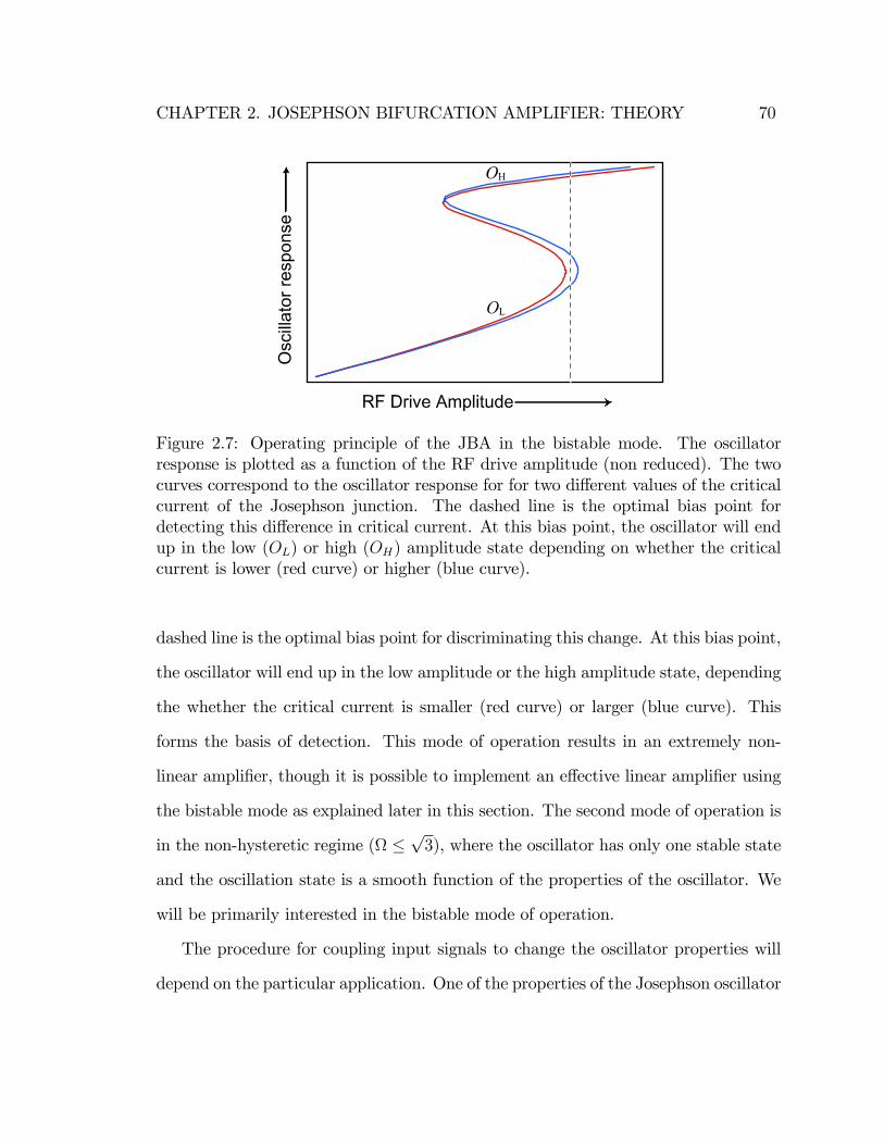
CHAPTER 2. JOSEPHSON BIFURCATION AMPLIFIER: THEORY 70
Figure 2.7: Operating principle of the JBA in the bistable mode. The oscillatorresponse is plotted as a function of the RF drive amplitude (non reduced). The twocurves correspond to the oscillator response for for two di¤erent values of the criticalcurrent of the Josephson junction. The dashed line is the optimal bias point fordetecting this di¤erence in critical current. At this bias point, the oscillator will endup in the low (OL) or high (OH) amplitude state depending on whether the criticalcurrent is lower (red curve) or higher (blue curve).
dashed line is the optimal bias point for discriminating this change. At this bias point,
the oscillator will end up in the low amplitude or the high amplitude state, depending
the whether the critical current is smaller (red curve) or larger (blue curve). This
forms the basis of detection. This mode of operation results in an extremely non-
linear ampli�er, though it is possible to implement an e¤ective linear ampli�er using
the bistable mode as explained later in this section. The second mode of operation is
in the non-hysteretic regime ( �p3), where the oscillator has only one stable state
and the oscillation state is a smooth function of the properties of the oscillator. We
will be primarily interested in the bistable mode of operation.
The procedure for coupling input signals to change the oscillator properties will
depend on the particular application. One of the properties of the Josephson oscillator
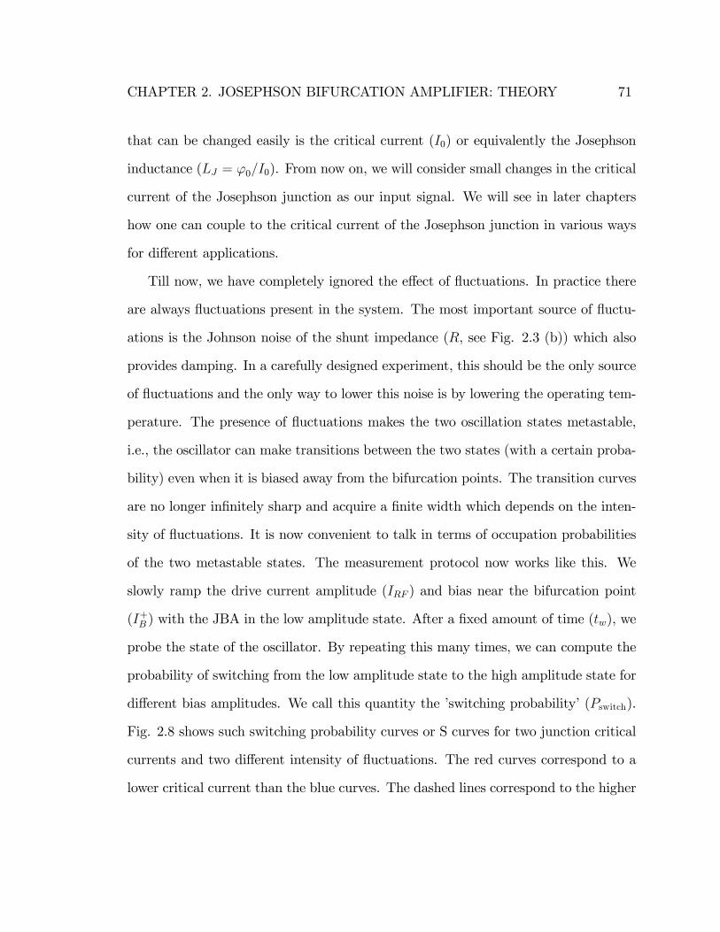
CHAPTER 2. JOSEPHSON BIFURCATION AMPLIFIER: THEORY 71
that can be changed easily is the critical current (I0) or equivalently the Josephson
inductance (LJ = '0=I0). From now on, we will consider small changes in the critical
current of the Josephson junction as our input signal. We will see in later chapters
how one can couple to the critical current of the Josephson junction in various ways
for di¤erent applications.
Till now, we have completely ignored the e¤ect of �uctuations. In practice there
are always �uctuations present in the system. The most important source of �uctu-
ations is the Johnson noise of the shunt impedance (R, see Fig. 2.3 (b)) which also
provides damping. In a carefully designed experiment, this should be the only source
of �uctuations and the only way to lower this noise is by lowering the operating tem-
perature. The presence of �uctuations makes the two oscillation states metastable,
i.e., the oscillator can make transitions between the two states (with a certain proba-
bility) even when it is biased away from the bifurcation points. The transition curves
are no longer in�nitely sharp and acquire a �nite width which depends on the inten-
sity of �uctuations. It is now convenient to talk in terms of occupation probabilities
of the two metastable states. The measurement protocol now works like this. We
slowly ramp the drive current amplitude (IRF ) and bias near the bifurcation point
(I+B ) with the JBA in the low amplitude state. After a �xed amount of time (tw), we
probe the state of the oscillator. By repeating this many times, we can compute the
probability of switching from the low amplitude state to the high amplitude state for
di¤erent bias amplitudes. We call this quantity the �switching probability�(Pswitch).
Fig. 2.8 shows such switching probability curves or S curves for two junction critical
currents and two di¤erent intensity of �uctuations. The red curves correspond to a
lower critical current than the blue curves. The dashed lines correspond to the higher
CHAPTER 2. JOSEPHSON BIFURCATION AMPLIFIER: THEORY 72
Figure 2.8: Switching probability or S curves indicate the probability of the JBAswitching from the low amplitude state to the high amplitude when biased near theupper bifurcation point (�+B). S curves are plotted as a function of the bias ampli-tude. Solid lines correspond to lower intensity of �uctuations while the dashed linescorrespond to higher intenstity of �uctuations. The red and blue curves correspondto di¤erent critical currents of the junction with the red one being lower than theblue one. The change in switching probability (�Pswitch) for a given change in criticalcurrent is smaller for larger intensity of �uctuations.
intensity of �uctuations. We note that the change in switching probability (�Pswitch)
for a given change in critical current gets smaller when the intensity of �uctuations
gets larger.
Small changes in critical current now result in small changes in switching proba-
bility. This mapping is linear for small changes and can be the basis of building an
e¤ective linear ampli�er. Note that the switching probability is an average quantity
and requires several measurements of the state of the oscillator. So the JBA can
act as a linear ampli�er for small, slow changes in critical current permitting sev-
eral preparations and measurements of the oscillator state before the critical current
changes signi�cantly. For detecting changes in a single measurement without too
much uncertainty, the shift in the S curve due that change in critical current must be
CHAPTER 2. JOSEPHSON BIFURCATION AMPLIFIER: THEORY 73
comparable to its width. In order to compute S curves and measurement sensitivity,
we need to compute the �uctuation induced transition rates between the metastable
states. This will be the subject of the next section.
2.3.2 Transition Rates
The theory of �uctuation induced transitions between metastable states in a driven
non-linear oscillator has been the subject of several papers [61, 27, 62] and the transi-
tion rates have been computed by di¤erent techniques. We will present results based
on the method followed in reference [27] because it provides easy to use formulae.
The starting point is the equation of motion for the driven Josephson junction
(2.1), but now we will include a noise term which is responsible for the transitions
between the metastable states
CS'0d2�(t)
dt2+'0R
d�(t)
dt+ I0 sin(�(t)) = I(t) + IN(t): (2.20)
Here IN(t) is the noise current corresponding to the Johnson noise in the resistor R
at temperature T . The noise current is white with a correlation function given by
hIN(t)IN(0)i =2kBT
R�(t) (2.21)
where T is the temperature of the resistor R and �(t) is the Dirac delta function [60].
Using the procedure outlined in section 2.2.1 we can arrive at the following equation
of motion for the complex amplitude u
du
d�= � u
� u
�juj2 � 1
�� ip� +~{N (�) (2.22)
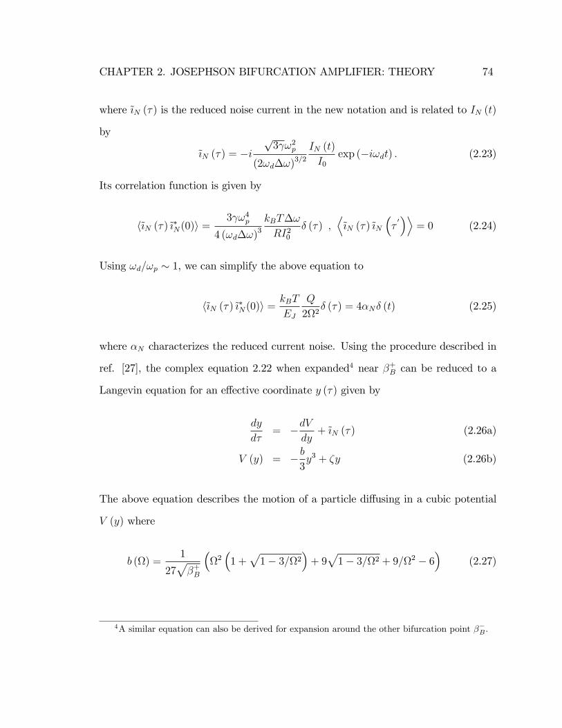
CHAPTER 2. JOSEPHSON BIFURCATION AMPLIFIER: THEORY 74
where ~{N (�) is the reduced noise current in the new notation and is related to IN (t)
by
~{N (�) = �ip3 !2p
(2!d�!)3=2
IN (t)
I0exp (�i!dt) : (2.23)
Its correlation function is given by
h~{N (�)~{�N(0)i =3 !4p
4 (!d�!)3
kBT�!
RI20� (�) ;
D~{N (�)~{N
��0�E= 0 (2.24)
Using !d=!p � 1, we can simplify the above equation to
h~{N (�)~{�N(0)i =kBT
EJ
Q
22� (�) = 4�N� (t) (2.25)
where �N characterizes the reduced current noise. Using the procedure described in
ref. [27], the complex equation 2.22 when expanded4 near �+B can be reduced to a
Langevin equation for an e¤ective coordinate y (�) given by
dy
d�= �dV
dy+~{N (�) (2.26a)
V (y) = � b3y3 + �y (2.26b)
The above equation describes the motion of a particle di¤using in a cubic potential
V (y) where
b () =1
27p�+B
�2�1 +
p1� 3=2
�+ 9p1� 3=2 + 9=2 � 6
�(2.27)
4A similar equation can also be derived for expansion around the other bifurcation point ��B .
CHAPTER 2. JOSEPHSON BIFURCATION AMPLIFIER: THEORY 75
Figure 2.9: Metapotential for the e¤ective slow coordinate. Its form is cubic when� ! �+B. The minima at �
p�=b corresponds to the low amplitude state while the
maxima at +p�=b corresponds to the unstable solution also known as the saddle
point (in phase space).
� (; �) =1
2
�+B � �p�+B
(2.28)
When the system is biased near a bifurcation point, its motion becomes over-
damped and one of the coordinates becomes much slower than all the other time
scales in the problem [27]. Consequently, the equation describing the dynamics can
be simpli�ed and the multidimensional equation 2.22 can be reduced to a simple
1-D motion of an e¤ective slow coordinate 2.26a. This separation of time scales is
discussed using a di¤erent approach in chapter 7.
For bias points such that � > 0, i.e., � < �+B, the potential V (y) has a local
minima and a saddle point at �p�=b respectively (see Fig. 2.9). The local minima
corresponds to the low amplitude state of the JBA while the saddle point is the
unstable solution (see section 2.2.1). The escape problem has now been reduced to a

CHAPTER 2. JOSEPHSON BIFURCATION AMPLIFIER: THEORY 76
standard Kramer�s [63, 64] problem for escape over barrier. It is now straightforward
to write down the escape rate from the low amplitude state of the JBA and it has an
Arrhenius like form given by
�RFesc =!RFa2�
exp
���URFesckBT
�(2.29)
where the exponent has been written as the ratio of an e¤ective barrier energy (�URFesc )
over thermal energy (kBT ). !RFa is called the attempt frequency (or inverse equili-
bration time) and is given by
!RFa = 2pb� (2.30)
while the expression for the barrier height is given by
�URFesc = kBT�V
�N=4
3
�3=2
b1=21
�N: (2.31)
Using equations 2.25,2.27 and 2.28 in equations 2.30 and 2.31, and simplifying5 in the
limit of large detuning >> 1, we arrive at the following expressions
!RFa = !RFa0
�1�
�IRF=I
+B
�2�1=2(2.32a)
�U = URFesc
�1�
�IRF=I
+B
�2�3=2(2.32b)
5See Appendix A for expressions without this approximation

CHAPTER 2. JOSEPHSON BIFURCATION AMPLIFIER: THEORY 77
where
!RFa0 =2
3p3
�!2
�(2.33a)
URFesc =32
9p3EJ
Q: (2.33b)
As expected for a cubic potential, the barrier height goes to zero with a 3=2 power law
as one approaches the bifurcation point. It is important to note that the Kramer�s
escape rate given by equation 2.29 is valid when �URFesc =kBT >> 1, i.e., only in the
limit of small escape rate [63].
The above expressions illustrate the dependence of the escape rate on various
parameters of the experiment. The dominant e¤ect comes due to changes in the
barrier height as it is inside the exponential. The drive amplitude IRF is one obvious
way of controlling the escape rate but we also see its dependence on the critical current
of the junction via various parameters (EJ = '0I0; !p = (I0='0CS)1=2; I+B (I0)). This
provides for a mechanism to detect changes in critical current via changes in switching
probability. We will discuss the sensitivity of the JBA to changes in critical current
in the next section.
2.3.3 Measurement sensitivity
There are two important quantities which go into determining the sensitivity of the
JBA to changes in critical current. The �rst quantity is the variation of the bifurcation
current I+B with critical current I0. This quantity for >> 1 can be written as follows
@I+B@I0
=I+BI0
3
4�: (2.34)

CHAPTER 2. JOSEPHSON BIFURCATION AMPLIFIER: THEORY 78
We can reorder the above equation in the following way
@I+B=I+B
@I0=I0=3
4�(2.35)
and note that the fractional variation in the bifurcation current (@I+B=IB) is always
bigger than the fractional variation in critical current (@I0=I0) since 3=4� > 1.
We introduced the idea of a switching probability curve or an S-curve in section
2.3.1. The width of the S-curve which depends on the intensity of �uctuations (given
by temperature T ) is the second quantity which determines the sensitivity of the
JBA. We will now de�ne this mathematically. Since we know the escape rate from
the low amplitude state to the high amplitude state of the JBA, we can de�ne the
probability of switching in a given time tw
Pswitch(IRF ; I0) = 1� exp��tw�RFesc (IRF ; I0)
�(2.36)
where Pswitch(IRF ; I0) has been de�ned as function of two parameters - the drive
amplitude IRF and the critical current I0 as we are interested in the variation of
Pswitch with respect to these two parameters. The S-curve is basically the plot of
Pswitch v.s. IRF for a given I0 (Fig. 5.11). In order to compute the sensitivity, we
need to calculate @Pswitch=@I0, which is given by
@Pswitch@I0
= �s1
I0
�URFesckBT
�2=3�I0I+B
@I+B@I0
�(2.37)
where �s � 1 is a scaling factor which depends weakly on the operating parameters.
We can now compute the smallest change in critical current �I0 that can be resolved
CHAPTER 2. JOSEPHSON BIFURCATION AMPLIFIER: THEORY 79
(�Pswitch � 1) in a single measurement
�I0 =
�@Pswitch@I0
��1(2.38)
This is can be expressed in terms of a current sensitivity SI0(in A/pHz) given a time
tpulse by the following equation
SI0 = �I0ptpulse =
�@Pswitch@I0
��1ptpulse (2.39)
The time tpulse is the total time of a single measurement which includes the time to
energize the JBA, the wait time tw, the time to record the oscillation state and the
time to ramp down the JBA. This time scale is set by the inverse damping rate � of
the JBA and we can write
tpulse = �po1
2�(2.40)
where �po � 10 is the pulse overhead factor. We can now write down the full expression
for the sensitivity as
SI0 =32=3
4p2
p�po
�s
1p�I1=30
�kBT
'0
�2=3�1=3 (2.41)
We note that the sensitivity depends quite weakly on most parameters, the strongest
being the temperature (T 2=3). The dependence on I0 is quite weak (I1=30 ) which
means that there is �exibility in choosing the value of junction critical current. An
important point to be noted is that the above analysis involves many approximations
which have been used to simplify calculations and see trends clearly. Often, many of
these approximations become too crude in real experiments and the only way to get

CHAPTER 2. JOSEPHSON BIFURCATION AMPLIFIER: THEORY 80
accurate predictions is to do full numerical simulations (Appendix C). Nevertheless,
the above formulae serve as a guide to the phenomena and provide quick estimates.
Chapter 3
Josephson Bifurcation Ampli�er: Experiments
In this chapter, we will discuss the experiments that were carried out to characterize
the performance of the Josephson Bifurcation Ampli�er. We will begin by discussing
the experimental setup and then go on to describe the measurement of the Josephson
oscillator resonance in the linear and non-linear regime. The hysteresis and bista-
bility measurements of the JBA will then be discussed. We will then describe the
experiments implementing the JBA as a sensitive detector and also discuss the noise
and sensitivity issues. Finally, we will discuss some practical issues concerning the
successful implementation of the JBA.
3.1 Experimental setup
The basic experiment that was carried out to probe the properties of the Josephson
oscillator was a phase-sensitive microwave re�ection experiment. A microwave signal
is sent via a transmission line to the oscillator, and the signal which is re�ected from
the oscillator is ampli�ed and its relative magnitude and phase recorded. For an ideal
81

CHAPTER 3. JOSEPHSON BIFURCATION AMPLIFIER: EXPTS 82
electrical oscillator made with dissipationless inductors and capacitors, the magnitude
of the re�ected signal is the same as the incident magnitude, and all the information
is contained in the relative phase of the re�ected signal.
The Josephson junction is the only known electrical element which remains non-
linear and non-dissipative at arbitrarily low temperatures. Typical junction fabrica-
tion parameters limit the plasma frequency of the Josephson oscillator to the 20 - 100
GHz range where techniques for addressing junction dynamics are inconvenient. We
have chosen to shunt the junction by a capacitive admittance to lower the plasma
frequency by more than an order of magnitude and attain a frequency in 1-2 GHz
range (microwave L-band). In this frequency range, a simple on-chip electrodynamic
environment with minimum parasitic elements can be implemented, and the hardware
for precise signal generation and processing is readily available.
Sample LJ(nH) !p=2�(GHz) CS(pF) LS(nH) RS ()1 0:28 1:18 39� 1 0:20� :02 0:82 0:18 1:25 30� 4 0:34� :04 0:82a 0:17 1:66 18� 1 0:32� :02 0:83 0:32 1:64 16� 1 0:27� :02 � 0:04 0:38 1:81 19� 1 0:03� :02 � 0:025 0:40 1:54 19� 1 0:15� :02 � 0:06 0:28 1:80 27� 1 0:01� :02 � 0:0
Table 3.1: Sample parameters. LJ = '0=I0 and !p are measured values. CS and LSare �t values to the data. Samples 1,2 and 2a have a 100 nm thick Au underlayer,sample 3 has a 50 nm thick Nb underlayer, sample 4 has a 1 �m thick Cu underlayer,and sample 5 has a 200 nm thick Nb underlayer.
In the �rst step of sample fabrication, a metallic underlayer �either a normal metal
(Au, Cu) or a superconductor (Nb) �was deposited on a silicon substrate to form
one plate of the shunting capacitor, followed by the deposition of an insulating Si3N4
layer which is the dielectric material in the capacitor. Using e-beam lithography and
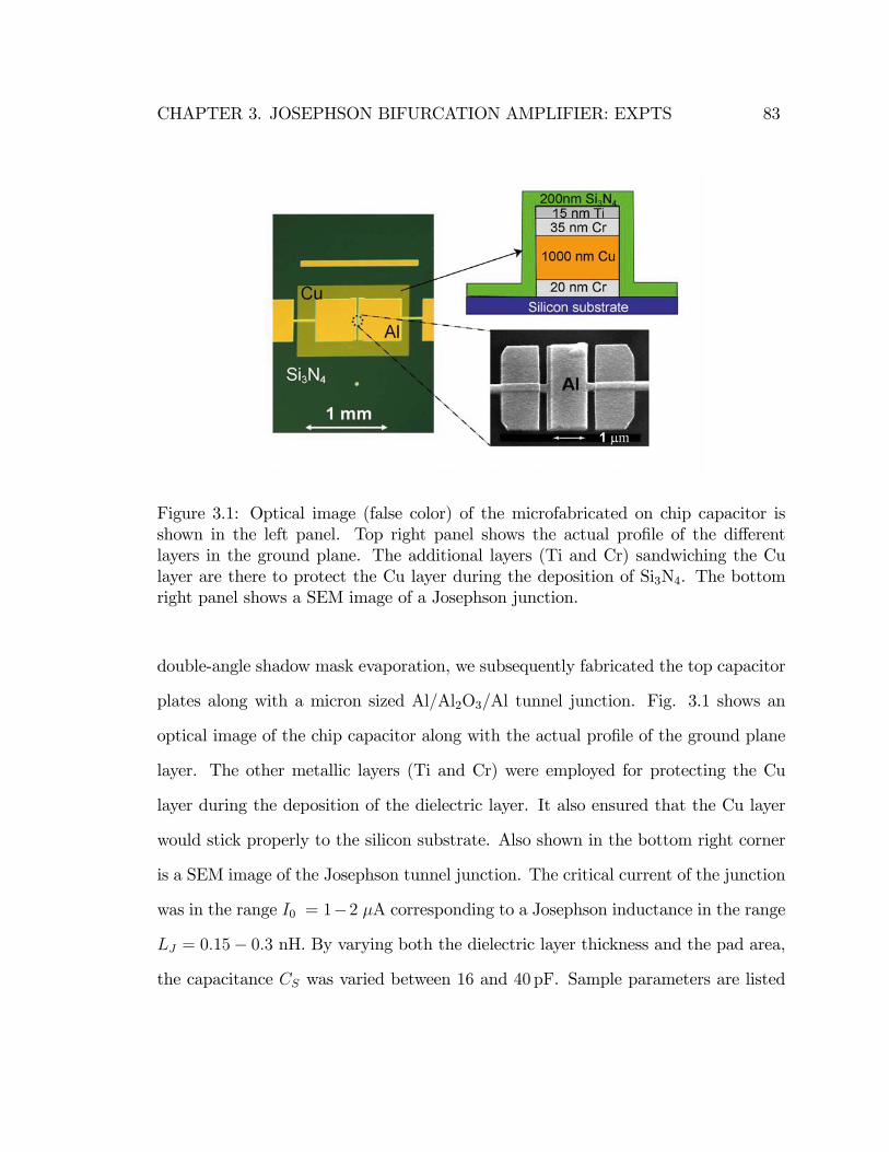
CHAPTER 3. JOSEPHSON BIFURCATION AMPLIFIER: EXPTS 83
Figure 3.1: Optical image (false color) of the microfabricated on chip capacitor isshown in the left panel. Top right panel shows the actual pro�le of the di¤erentlayers in the ground plane. The additional layers (Ti and Cr) sandwiching the Culayer are there to protect the Cu layer during the deposition of Si3N4. The bottomright panel shows a SEM image of a Josephson junction.
double-angle shadow mask evaporation, we subsequently fabricated the top capacitor
plates along with a micron sized Al=Al2O3=Al tunnel junction. Fig. 3.1 shows an
optical image of the chip capacitor along with the actual pro�le of the ground plane
layer. The other metallic layers (Ti and Cr) were employed for protecting the Cu
layer during the deposition of the dielectric layer. It also ensured that the Cu layer
would stick properly to the silicon substrate. Also shown in the bottom right corner
is a SEM image of the Josephson tunnel junction. The critical current of the junction
was in the range I0 = 1�2 �A corresponding to a Josephson inductance in the range
LJ = 0:15� 0:3 nH. By varying both the dielectric layer thickness and the pad area,
the capacitance CS was varied between 16 and 40 pF. Sample parameters are listed
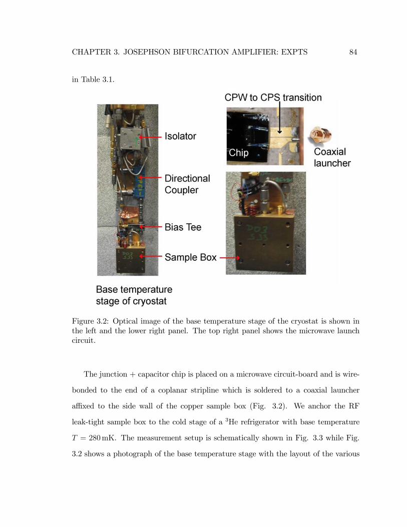
CHAPTER 3. JOSEPHSON BIFURCATION AMPLIFIER: EXPTS 84
in Table 3.1.
Figure 3.2: Optical image of the base temperature stage of the cryostat is shown inthe left and the lower right panel. The top right panel shows the microwave launchcircuit.
The junction + capacitor chip is placed on a microwave circuit-board and is wire-
bonded to the end of a coplanar stripline which is soldered to a coaxial launcher
a¢ xed to the side wall of the copper sample box (Fig. 3.2). We anchor the RF
leak-tight sample box to the cold stage of a 3He refrigerator with base temperature
T = 280mK. The measurement setup is schematically shown in Fig. 3.3 while Fig.
3.2 shows a photograph of the base temperature stage with the layout of the various

CHAPTER 3. JOSEPHSON BIFURCATION AMPLIFIER: EXPTS 85
microwave components.
Figure 3.3: Schematic of the measurement setup. Thick lines correspond to 50coaxial transmission lines. The network analyzer is used for CW measurements. Forprobing the dynamics (section 3.3), the pulse generator and phase detector were used.A lumped element model for the junction chip and measurement line is shown. Thetwo ideal current sources actually represent external sources.
Microwave excitation signals are generated by a HP 8722D vector network ana-
lyzer or a pulse generator and are coupled to the sample via the -13 dB side port
of a directional coupler after passing through cryogenic attenuators. The re�ected
microwave signal passes through the direct port of the coupler, and is ampli�ed �rst
using a cryogenic 1:20� 1:85GHz HEMT ampli�er with noise temperature TN = 4K
CHAPTER 3. JOSEPHSON BIFURCATION AMPLIFIER: EXPTS 86
before returning to the network analyzer or a phase detector1. The isolators allow
microwave signals to propagate only in one direction, preventing the HEMT ampli-
�er noise from reaching the sample. The attenuators on the input line carry out a
similar function by attenuating the thermal noise from higher temperature stages.
In later experiments we have also used various kinds of microwave �lters to prevent
spurious noise from reaching the sample. All this ensures that the �uctuations felt by
the sample correspond to the temperature of the cold stage to which it is anchored.
This is important for maximizing the sensitivity of the JBA when implemented as a
readout. A DC bias current can also be applied to the junction by way of a bias tee
and a passive �lter network.
3.2 Frequency domain measurements
3.2.1 Linear resonance
We locate the linear plasma resonance by sweeping the excitation frequency from 1
to 2 GHz and measuring the re�ection coe¢ cient
�R(!d) = Iin=Iout ej� = (Z(!d)� Z0)=(Z(!d) + Z0) (3.1)
where Z0 = 50 is the characteristic impedance of our transmission lines and Z(!d)
is the impedance presented to the analyzer by the chip and the measurement lines.
For an ideal LC resonator without intrinsic dissipation, we expect a phase shift �� =
�!d�!p��!d�!p = 2�, which we veri�ed by placing a chip capacitor and an inductive
1A pulse generator and a phase detector were used for the time domain measurements describedsection 3.3.
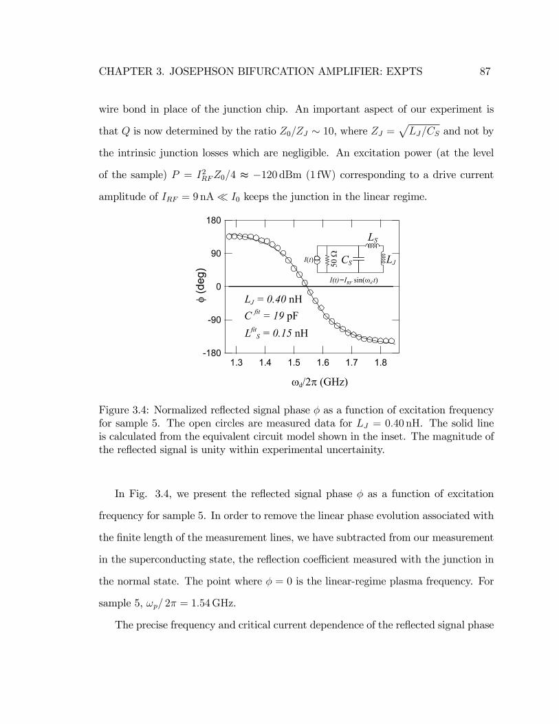
CHAPTER 3. JOSEPHSON BIFURCATION AMPLIFIER: EXPTS 87
wire bond in place of the junction chip. An important aspect of our experiment is
that Q is now determined by the ratio Z0=ZJ � 10, where ZJ =pLJ=CS and not by
the intrinsic junction losses which are negligible. An excitation power (at the level
of the sample) P = I2RFZ0=4 t �120 dBm (1 fW) corresponding to a drive current
amplitude of IRF = 9nA� I0 keeps the junction in the linear regime.
Figure 3.4: Normalized re�ected signal phase � as a function of excitation frequencyfor sample 5. The open circles are measured data for LJ = 0:40 nH. The solid lineis calculated from the equivalent circuit model shown in the inset. The magnitude ofthe re�ected signal is unity within experimental uncertainity.
In Fig. 3.4, we present the re�ected signal phase � as a function of excitation
frequency for sample 5. In order to remove the linear phase evolution associated with
the �nite length of the measurement lines, we have subtracted from our measurement
in the superconducting state, the re�ection coe¢ cient measured with the junction in
the normal state. The point where � = 0 is the linear-regime plasma frequency. For
sample 5, !p= 2� = 1:54GHz.
The precise frequency and critical current dependence of the re�ected signal phase

CHAPTER 3. JOSEPHSON BIFURCATION AMPLIFIER: EXPTS 88
of our samples can be accounted for by a 3-element model for the electrodynamic
environment seen by the junction. This lumped element model is shown in the lower
right corner of Fig. 3.3. The parasitic inductance LS and resistance RS model the
non-ideality of the shunting capacitor CS. They arise from the imperfect screening of
currents �owing in the capacitor plates and the �nite conductivity of these plates. The
plasma frequency in the linear regime is determined by the total inductance LJ +LS
and capacitance Ceff = CJ + CS ' CS; and is given by the following relation:
�1
!p
�2= CS(LJ + LS) =
'0CSI0
+ CSLS: (3.2)
We thus plot (2�=!p)2 versus 1=I0 = LJ='0 in Fig. 3.5 for samples 1, 2, 2a, 4 and
5. As the critical current is decreased by applying a magnetic �eld, the junction
inductance increases, and the plasma frequency is reduced. For each sample, a linear
�t to the data of Fig. 3.5 yields the values of CS and LS (see table 3.1). The �t values
for CS agree well with simple estimates made from the sample geometry. Samples 1
and 2 have nominally the same capacitance but di¤erent critical current, and hence
lie approximately on the same line in Fig. 3.5.
A total of four capacitive pads were used to make the shunting capacitor in samples
1 and 2, and after initial measurements, we scratched o¤two of the pads from sample 2
to obtain sample 2a, and the resulting capacitance is indeed halved. For samples with
a thin underlayer (1,2 and 3), a stray inductance in the range LS = 0:20 � 0:34 nH
is observed. For samples 4 and 5 with a signi�cantly thicker underlayer, LS was
reduced to 0:026 nH and 0:15 nH respectively. This behavior is consistent with the
calculated screening properties of our thin �lms. To verify that the values of CS and
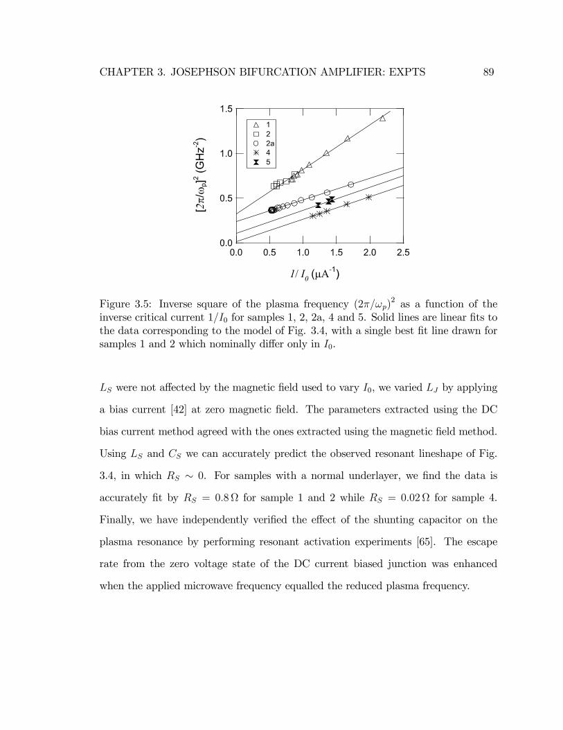
CHAPTER 3. JOSEPHSON BIFURCATION AMPLIFIER: EXPTS 89
Figure 3.5: Inverse square of the plasma frequency (2�=!p)2 as a function of the
inverse critical current 1=I0 for samples 1, 2, 2a, 4 and 5. Solid lines are linear �ts tothe data corresponding to the model of Fig. 3.4, with a single best �t line drawn forsamples 1 and 2 which nominally di¤er only in I0.
LS were not a¤ected by the magnetic �eld used to vary I0, we varied LJ by applying
a bias current [42] at zero magnetic �eld. The parameters extracted using the DC
bias current method agreed with the ones extracted using the magnetic �eld method.
Using LS and CS we can accurately predict the observed resonant lineshape of Fig.
3.4, in which RS � 0. For samples with a normal underlayer, we �nd the data is
accurately �t by RS = 0:8 for sample 1 and 2 while RS = 0:02 for sample 4.
Finally, we have independently veri�ed the e¤ect of the shunting capacitor on the
plasma resonance by performing resonant activation experiments [65]. The escape
rate from the zero voltage state of the DC current biased junction was enhanced
when the applied microwave frequency equalled the reduced plasma frequency.
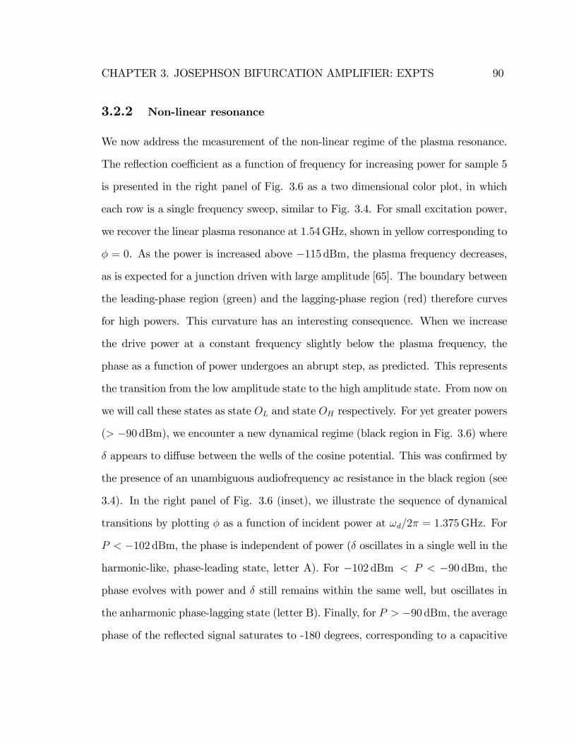
CHAPTER 3. JOSEPHSON BIFURCATION AMPLIFIER: EXPTS 90
3.2.2 Non-linear resonance
We now address the measurement of the non-linear regime of the plasma resonance.
The re�ection coe¢ cient as a function of frequency for increasing power for sample 5
is presented in the right panel of Fig. 3.6 as a two dimensional color plot, in which
each row is a single frequency sweep, similar to Fig. 3.4. For small excitation power,
we recover the linear plasma resonance at 1:54GHz, shown in yellow corresponding to
� = 0. As the power is increased above �115 dBm, the plasma frequency decreases,
as is expected for a junction driven with large amplitude [65]. The boundary between
the leading-phase region (green) and the lagging-phase region (red) therefore curves
for high powers. This curvature has an interesting consequence. When we increase
the drive power at a constant frequency slightly below the plasma frequency, the
phase as a function of power undergoes an abrupt step, as predicted. This represents
the transition from the low amplitude state to the high amplitude state. From now on
we will call these states as state OL and state OH respectively. For yet greater powers
(> �90 dBm), we encounter a new dynamical regime (black region in Fig. 3.6) where
� appears to di¤use between the wells of the cosine potential. This was con�rmed by
the presence of an unambiguous audiofrequency ac resistance in the black region (see
3.4). In the right panel of Fig. 3.6 (inset), we illustrate the sequence of dynamical
transitions by plotting � as a function of incident power at !d=2� = 1:375GHz. For
P < �102 dBm, the phase is independent of power (� oscillates in a single well in the
harmonic-like, phase-leading state, letter A). For �102 dBm < P < �90 dBm, the
phase evolves with power and � still remains within the same well, but oscillates in
the anharmonic phase-lagging state (letter B). Finally, for P > �90 dBm, the average
phase of the re�ected signal saturates to -180 degrees, corresponding to a capacitive

CHAPTER 3. JOSEPHSON BIFURCATION AMPLIFIER: EXPTS 91
short circuit. This last value is expected if � hops randomly between wells, the e¤ect
of which is to neutralize the Josephson inductive admittance.
Figure 3.6: Normalized re�ected signal phase � (wrap-around color scheme) as afunction of excitation frequency !d=2� and excitation power P is shown for sample5. Experimental data is shown in the right panel while the left panel is the resultof numerical simulations. A vertical slice taken at !d=2� = 1:375 GHz (dashed line)shows the abrupt transition between two oscillation states of the system.
The value of the current IB for the A-B transition, which is a function of both
the relative detuning � = 1 � !d=!p and power P , is in good agreement with the
analytical theory which retains only the �rst anharmonic term in the cosine potential
(see chapter 2). For instance, the slope of the A-B transition line (equation 2.8 and
2.13) at the linecut in Fig. 3.6, dP (dBm)=d�(%) = 0:8 for the experiment while we
calculate its value to be 0:7. Furthermore, in measurements in which the power is
ramped in less than 100 ns, we veri�ed that the transition between dynamical states
is hysteretic, another prediction of the theory. To explain the complete frequency and
power dependence of the transitions shown in the right panel of Fig. 3.6, we have
CHAPTER 3. JOSEPHSON BIFURCATION AMPLIFIER: EXPTS 92
performed numerical simulations by solving the full circuit model of the lower right
corner of Fig. 3.3, including the exact junction non-linear constitutive relation. The
result of this calculation is shown in the left panel of Fig. 3.6. It correctly predicts the
variation of the plasma frequency with excitation power, and the boundaries of the
phase di¤usion region. The agreement between theory and experiment is remarkable
in view of the simplicity of the model which uses only measured parameters, and only
small di¤erences in the exact shape of region boundaries are observed2.
3.3 Time domain measurements
The measurements described so far characterized the time averaged response of the
Josephson oscillator under continuous microwave excitation. We will now describe
the experiments which probed the response of the JBA at short time scales (� 10
ns) under pulsed microwave excitation. Sample 6 was used for this experiment and
had a Josephson junction with critical current I0 = 1:17�A, an on-chip lithographic
capacitance CS = 27 pF resulting in a reduced plasma frequency !p=2� = 1:80GHz.
The stray elements LS and RS were negligible for this sample. The dynamics of
the transition between the two oscillation states were probed using microwave pulses,
generated by the amplitude modulation of a CW source with a phase-locked arbitrary
waveform generator with 1 ns resolution. As described in the previous section, the
re�ected signal from the sample was passed through a circulator at base temperature
T = 0:25K to a matched HEMT ampli�er at T = 4:2K. At room temperature, the
re�ected signal was further ampli�ed, mixed down to 100MHz and �nally digitally
2It is important to mention that the overall topology of Fig. 3.6 is not signi�cantly a¤ected bychanges in the parameter values within the bounds of Table 3.1
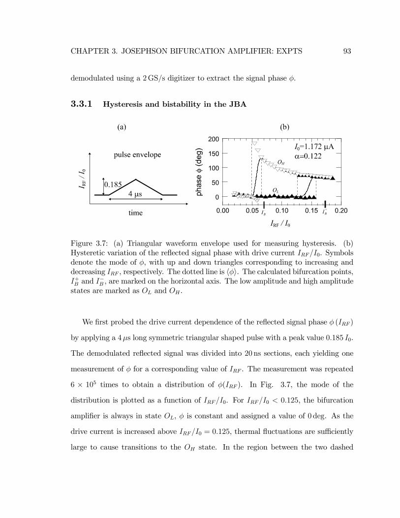
CHAPTER 3. JOSEPHSON BIFURCATION AMPLIFIER: EXPTS 93
demodulated using a 2GS=s digitizer to extract the signal phase �.
3.3.1 Hysteresis and bistability in the JBA
Figure 3.7: (a) Triangular waveform envelope used for measuring hysteresis. (b)Hysteretic variation of the re�ected signal phase with drive current IRF=I0. Symbolsdenote the mode of �, with up and down triangles corresponding to increasing anddecreasing IRF , respectively. The dotted line is h�i. The calculated bifurcation points,I+B and I
�B , are marked on the horizontal axis. The low amplitude and high amplitude
states are marked as OL and OH .
We �rst probed the drive current dependence of the re�ected signal phase � (IRF )
by applying a 4�s long symmetric triangular shaped pulse with a peak value 0:185 I0.
The demodulated re�ected signal was divided into 20 ns sections, each yielding one
measurement of � for a corresponding value of IRF . The measurement was repeated
6 � 105 times to obtain a distribution of �(IRF ). In Fig. 3.7, the mode of the
distribution is plotted as a function of IRF=I0. For IRF=I0 < 0:125, the bifurcation
ampli�er is always in state OL, � is constant and assigned a value of 0 deg. As the
drive current is increased above IRF=I0 = 0:125, thermal �uctuations are su¢ ciently
large to cause transitions to the OH state. In the region between the two dashed
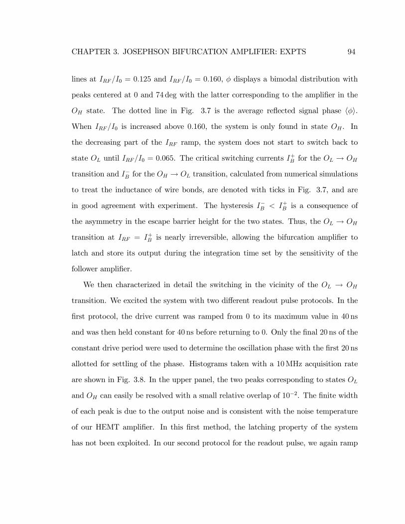
CHAPTER 3. JOSEPHSON BIFURCATION AMPLIFIER: EXPTS 94
lines at IRF=I0 = 0:125 and IRF=I0 = 0:160, � displays a bimodal distribution with
peaks centered at 0 and 74 deg with the latter corresponding to the ampli�er in the
OH state. The dotted line in Fig. 3.7 is the average re�ected signal phase h�i.
When IRF=I0 is increased above 0:160, the system is only found in state OH . In
the decreasing part of the IRF ramp, the system does not start to switch back to
state OL until IRF=I0 = 0:065. The critical switching currents I+B for the OL ! OH
transition and I�B for the OH ! OL transition, calculated from numerical simulations
to treat the inductance of wire bonds, are denoted with ticks in Fig. 3.7, and are
in good agreement with experiment. The hysteresis I�B < I+B is a consequence of
the asymmetry in the escape barrier height for the two states. Thus, the OL ! OH
transition at IRF = I+B is nearly irreversible, allowing the bifurcation ampli�er to
latch and store its output during the integration time set by the sensitivity of the
follower ampli�er.
We then characterized in detail the switching in the vicinity of the OL ! OH
transition. We excited the system with two di¤erent readout pulse protocols. In the
�rst protocol, the drive current was ramped from 0 to its maximum value in 40 ns
and was then held constant for 40 ns before returning to 0. Only the �nal 20 ns of the
constant drive period were used to determine the oscillation phase with the �rst 20 ns
allotted for settling of the phase. Histograms taken with a 10MHz acquisition rate
are shown in Fig. 3.8. In the upper panel, the two peaks corresponding to states OL
and OH can easily be resolved with a small relative overlap of 10�2. The �nite width
of each peak is due to the output noise and is consistent with the noise temperature
of our HEMT ampli�er. In this �rst method, the latching property of the system
has not been exploited. In our second protocol for the readout pulse, we again ramp
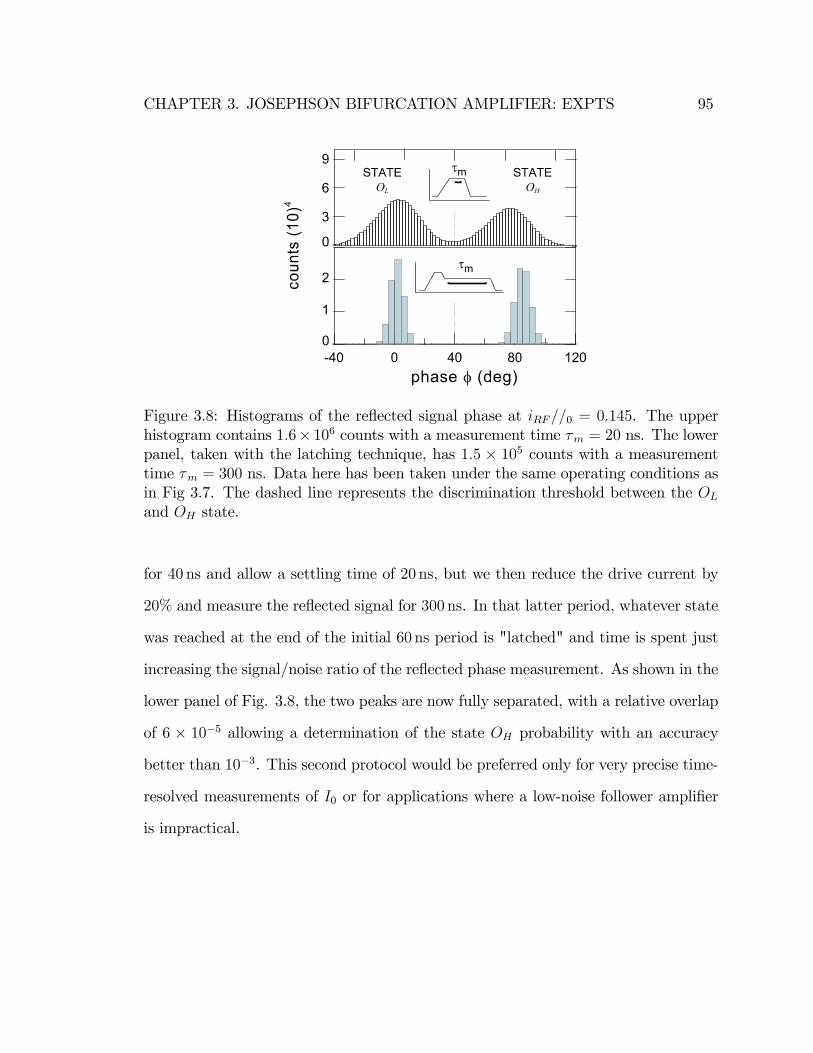
CHAPTER 3. JOSEPHSON BIFURCATION AMPLIFIER: EXPTS 95
Figure 3.8: Histograms of the re�ected signal phase at iRF==0 = 0:145. The upperhistogram contains 1:6� 106 counts with a measurement time �m = 20 ns. The lowerpanel, taken with the latching technique, has 1:5 � 105 counts with a measurementtime �m = 300 ns. Data here has been taken under the same operating conditions asin Fig 3.7. The dashed line represents the discrimination threshold between the OLand OH state.
for 40 ns and allow a settling time of 20 ns, but we then reduce the drive current by
20% and measure the re�ected signal for 300 ns. In that latter period, whatever state
was reached at the end of the initial 60 ns period is "latched" and time is spent just
increasing the signal/noise ratio of the re�ected phase measurement. As shown in the
lower panel of Fig. 3.8, the two peaks are now fully separated, with a relative overlap
of 6 � 10�5 allowing a determination of the state OH probability with an accuracy
better than 10�3. This second protocol would be preferred only for very precise time-
resolved measurements of I0 or for applications where a low-noise follower ampli�er
is impractical.
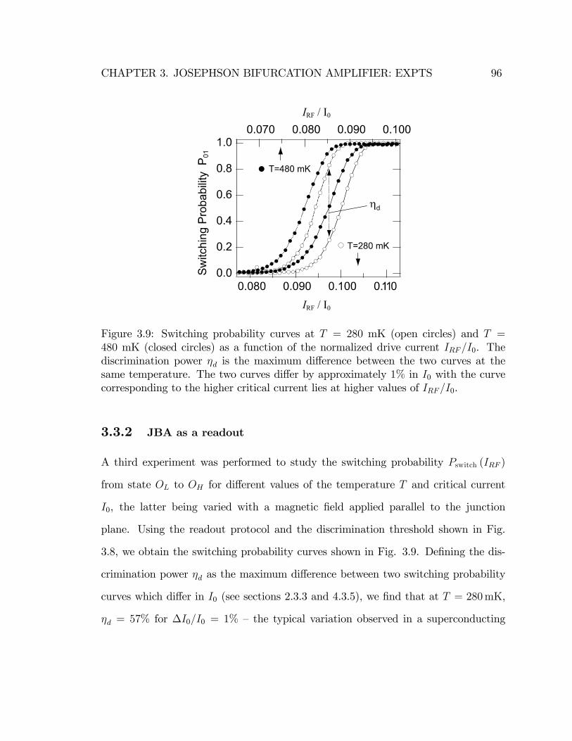
CHAPTER 3. JOSEPHSON BIFURCATION AMPLIFIER: EXPTS 96
Figure 3.9: Switching probability curves at T = 280 mK (open circles) and T =480 mK (closed circles) as a function of the normalized drive current IRF=I0. Thediscrimination power �d is the maximum di¤erence between the two curves at thesame temperature. The two curves di¤er by approximately 1% in I0 with the curvecorresponding to the higher critical current lies at higher values of IRF=I0.
3.3.2 JBA as a readout
A third experiment was performed to study the switching probability Pswitch (IRF )
from state OL to OH for di¤erent values of the temperature T and critical current
I0, the latter being varied with a magnetic �eld applied parallel to the junction
plane. Using the readout protocol and the discrimination threshold shown in Fig.
3.8, we obtain the switching probability curves shown in Fig. 3.9. De�ning the dis-
crimination power �d as the maximum di¤erence between two switching probability
curves which di¤er in I0 (see sections 2.3.3 and 4.3.5), we �nd that at T = 280mK,
�d = 57% for �I0=I0 = 1% �the typical variation observed in a superconducting
CHAPTER 3. JOSEPHSON BIFURCATION AMPLIFIER: EXPTS 97
charge-phase qubit [6]. The switching probability curves should shift according to
(�IB=IB)=(�I0=I0) = 3=4� (equation 2.35), which for our case takes the value 6.1.
In Fig. 3.9, the curves are shifted by 6%, which agrees well with this prediction.
For the case of the DC current biased junction, similar curves would shift only by
1%. Comparable discrimination power using DC switching has only been achieved in
these devices at T � 60mK: As the temperature is increased, the switching probabil-
ity curves broaden due to increased thermal �uctuations and the discriminating power
decreases: at T = 480mK, �d = 49%. Correspondingly, the discrimination increases
as the temperature is lowered. The experimentally achieved values of discrimination
power were in good agreement with the theoretical predictions and numerical simu-
lations. Numerical simulations of the combined JBA+qubit system will be discussed
in the next chapter.
As discussed in section 2.3.3, the sensitivity of the JBA as a detector of critical cur-
rent variations is determined by the width of the S-curves, which in turn is determined
by the e¤ective intensity of �uctuations felt by the JBA. A well designed experimental
setup will ensure that this intensity of �uctuations is set by the thermal/quantum
�uctuations corresponding to the operating temperature of the JBA. It is possible
to determine the e¤ective temperature felt by the JBA by carefully measuring the
escape rates from state OL to OH as a function of the various bias parameters. The
classical theory of escape was brie�y described in section 2.3.2. Chapter 7 describes
a theory of escape which is applicable both the classical (kBT >> ~!p) and quantum
(kBT >> ~!p) regimes. The escape measurements are described in chapter 8. These
measurements will help in determining the ultimate sensitivity of the JBA.
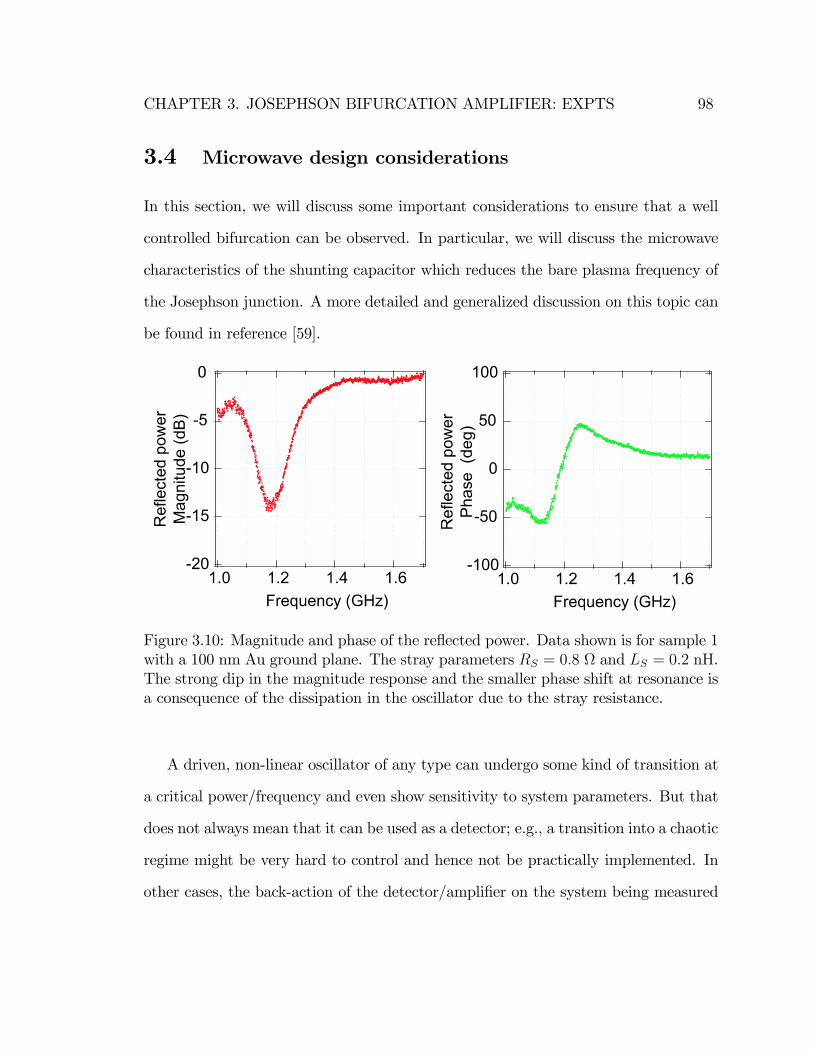
CHAPTER 3. JOSEPHSON BIFURCATION AMPLIFIER: EXPTS 98
3.4 Microwave design considerations
In this section, we will discuss some important considerations to ensure that a well
controlled bifurcation can be observed. In particular, we will discuss the microwave
characteristics of the shunting capacitor which reduces the bare plasma frequency of
the Josephson junction. A more detailed and generalized discussion on this topic can
be found in reference [59].
Figure 3.10: Magnitude and phase of the re�ected power. Data shown is for sample 1with a 100 nm Au ground plane. The stray parameters RS = 0:8 and LS = 0:2 nH.The strong dip in the magnitude response and the smaller phase shift at resonance isa consequence of the dissipation in the oscillator due to the stray resistance.
A driven, non-linear oscillator of any type can undergo some kind of transition at
a critical power/frequency and even show sensitivity to system parameters. But that
does not always mean that it can be used as a detector; e.g., a transition into a chaotic
regime might be very hard to control and hence not be practically implemented. In
other cases, the back-action of the detector/ampli�er on the system being measured

CHAPTER 3. JOSEPHSON BIFURCATION AMPLIFIER: EXPTS 99
might become uncontrolled. The kind of bifurcation described theoretically in the
previous chapter and experimentally in this one, is controllable and well behaved
as a function of bias parameters (frequency and power). In order to observe this
bifurcation phenomena and use it e¤ectively as a detector/ampli�er, we need to ensure
that the non-linear system is constructed correctly.
During the initial stages of this experiment, we realized that the design of the
shunting capacitor had to be implemented carefully to ensure that it behaved as
a capacitor at the relevant frequencies. Fabricating ideal, lumped circuit elements
operable at microwave frequencies is non-trivial. Typically, the lumped element will
have capacitance, inductance and resistance depending on how it is fabricated and
the frequencies at which it is being used. As we go to higher frequencies (> 5 GHz), it
is much easier and practical to use distributed circuit elements like transmission line
resonators. This was one of the reasons for the development of the Cavity Bifurcation
Ampli�er (CBA) which uses transmission line resonators with an embedded Josephson
junction to implement the non-linear oscillator [66].
The �rst generation of our microwave capacitors were made using a thin (100
nm) Au ground plane. This was followed by Nb ground planes (50 and 200 nm) and
then thick (1 �m) Cu. As discussed in section 3.1, imperfect screening currents in
the capacitor plates due to the �nite conductivity (Au and Cu) and thickness of the
ground planes, results in a stray inductance (LS) and a stray resistance (RS). The
inset shown in Fig. 3.3 depicts a model which accounts for the stray inductance and
resistance. The samples made with superconducting Nb ground planes did not have
any stray resistance while the data for samples with Au and Cu ground planes lead
to a value of RS = 0:8 and 0:02 respectively. The best results were obtained with
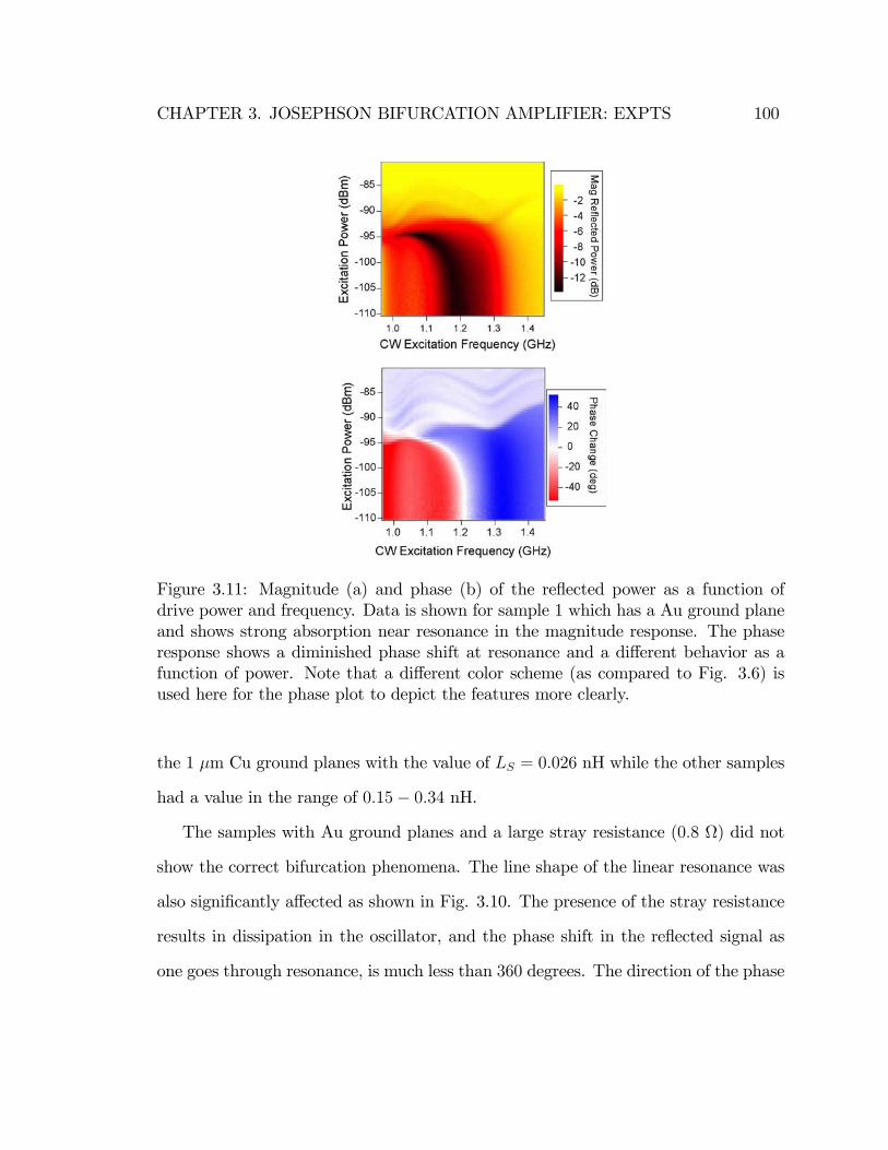
CHAPTER 3. JOSEPHSON BIFURCATION AMPLIFIER: EXPTS 100
Figure 3.11: Magnitude (a) and phase (b) of the re�ected power as a function ofdrive power and frequency. Data is shown for sample 1 which has a Au ground planeand shows strong absorption near resonance in the magnitude response. The phaseresponse shows a diminished phase shift at resonance and a di¤erent behavior as afunction of power. Note that a di¤erent color scheme (as compared to Fig. 3.6) isused here for the phase plot to depict the features more clearly.
the 1 �m Cu ground planes with the value of LS = 0:026 nH while the other samples
had a value in the range of 0:15� 0:34 nH.
The samples with Au ground planes and a large stray resistance (0:8 ) did not
show the correct bifurcation phenomena. The line shape of the linear resonance was
also signi�cantly a¤ected as shown in Fig. 3.10. The presence of the stray resistance
results in dissipation in the oscillator, and the phase shift in the re�ected signal as
one goes through resonance, is much less than 360 degrees. The direction of the phase
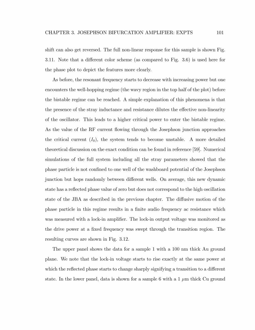
CHAPTER 3. JOSEPHSON BIFURCATION AMPLIFIER: EXPTS 101
shift can also get reversed. The full non-linear response for this sample is shown Fig.
3.11. Note that a di¤erent color scheme (as compared to Fig. 3.6) is used here for
the phase plot to depict the features more clearly.
As before, the resonant frequency starts to decrease with increasing power but one
encounters the well-hopping regime (the wavy region in the top half of the plot) before
the bistable regime can be reached. A simple explanation of this phenomena is that
the presence of the stray inductance and resistance dilutes the e¤ective non-linearity
of the oscillator. This leads to a higher critical power to enter the bistable regime.
As the value of the RF current �owing through the Josephson junction approaches
the critical current (I0), the system tends to become unstable. A more detailed
theoretical discussion on the exact condition can be found in reference [59]. Numerical
simulations of the full system including all the stray parameters showed that the
phase particle is not con�ned to one well of the washboard potential of the Josephson
junction but hops randomly between di¤erent wells. On average, this new dynamic
state has a re�ected phase value of zero but does not correspond to the high oscillation
state of the JBA as described in the previous chapter. The di¤usive motion of the
phase particle in this regime results in a �nite audio frequency ac resistance which
was measured with a lock-in ampli�er. The lock-in output voltage was monitored as
the drive power at a �xed frequency was swept through the transition region. The
resulting curves are shown in Fig. 3.12.
The upper panel shows the data for a sample 1 with a 100 nm thick Au ground
plane. We note that the lock-in voltage starts to rise exactly at the same power at
which the re�ected phase starts to change sharply signifying a transition to a di¤erent
state. In the lower panel, data is shown for a sample 6 with a 1 �m thick Cu ground
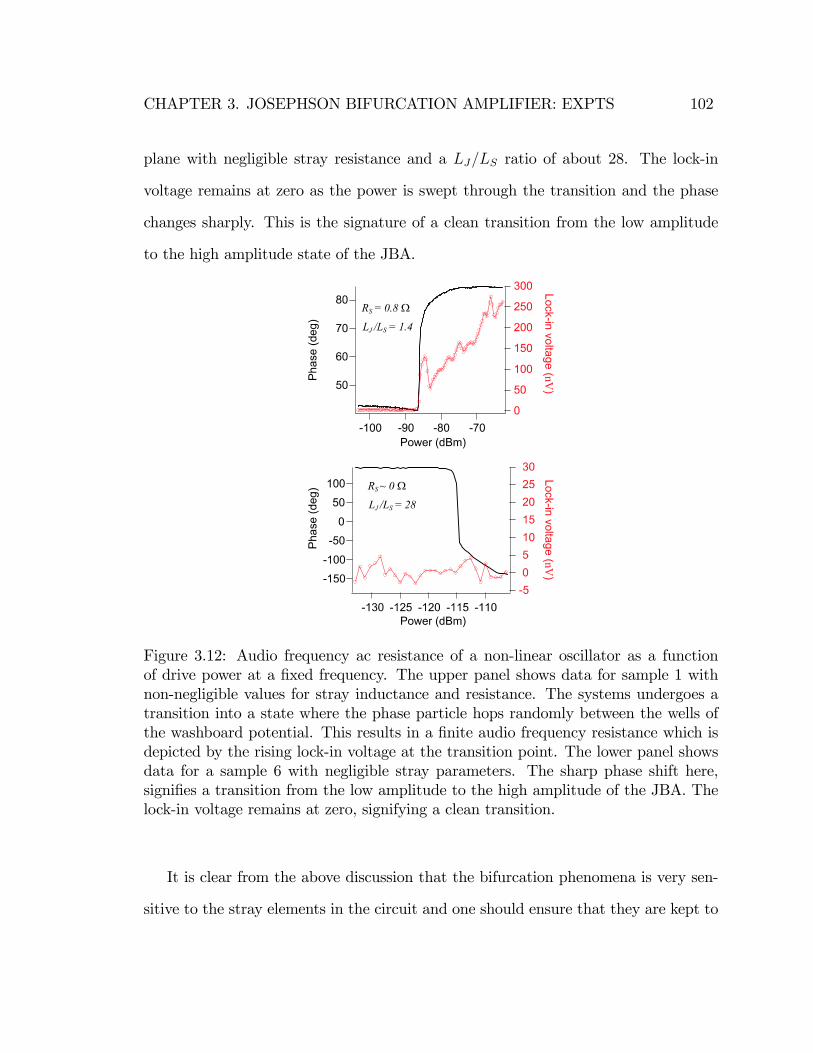
CHAPTER 3. JOSEPHSON BIFURCATION AMPLIFIER: EXPTS 102
plane with negligible stray resistance and a LJ=LS ratio of about 28. The lock-in
voltage remains at zero as the power is swept through the transition and the phase
changes sharply. This is the signature of a clean transition from the low amplitude
to the high amplitude state of the JBA.
Figure 3.12: Audio frequency ac resistance of a non-linear oscillator as a functionof drive power at a �xed frequency. The upper panel shows data for sample 1 withnon-negligible values for stray inductance and resistance. The systems undergoes atransition into a state where the phase particle hops randomly between the wells ofthe washboard potential. This results in a �nite audio frequency resistance which isdepicted by the rising lock-in voltage at the transition point. The lower panel showsdata for a sample 6 with negligible stray parameters. The sharp phase shift here,signi�es a transition from the low amplitude to the high amplitude of the JBA. Thelock-in voltage remains at zero, signifying a clean transition.
It is clear from the above discussion that the bifurcation phenomena is very sen-
sitive to the stray elements in the circuit and one should ensure that they are kept to

CHAPTER 3. JOSEPHSON BIFURCATION AMPLIFIER: EXPTS 103
a minimum. Irrespective of the stray parameters, the well-hopping regime is always
encountered at high enough drive power (the black region in Fig. 3.6 and the white
region in Fig. 3.11). The stray parameters determine whether one can approach the
critical power required for observing the bifurcation phenomena before running into
the well-hopping regime. For future experiments, we decided on using a 500 nm thick
Cu ground plane for the capacitors. This provided us with a small stray resistance
(< 0.05 ) and LJ=LS ratio greater than than 20. The thickness of the ground plane
was reduced from 1 �m to make the fabrication procedure easier. These parameters
provided us with a clean bifurcation and su¢ cient room to vary drive frequency and
power without running into the well-hopping regime. Furthermore, we noted that the
transition into the well-hopping state showed su¢ cient sensitivity to system parame-
ters and could in principle be used for making a detector. But the di¤usive nature
of the phase particle in this regime can lead to strong back-action e¤ects. This rules
out its application for measuring delicate systems like superconducting qubits. We
will discuss these back-action e¤ects on qubits in chapter 6.
In conclusion, we have performed a novel, phase-sensitive, microwave experiment
demonstrating that the Josephson plasma oscillation can transition between the two
dynamical states predicted for a driven non-linear system. Using di¤erent samples,
we have shown that this dynamical phenomenon is stable, reproducible and can be
precisely controlled, thus opening the possibility for practical applications like am-
pli�cation. We have also studied its response in the time domain and successfully
implemented a readout protocol to discriminate small changes in critical current of
the Josephson junction. With the JBA operating at T = 280mK, it is possible to
resolve with a signal/noise ratio of 1 a 10 nA variation in I0 in a total time � 80
CHAPTER 3. JOSEPHSON BIFURCATION AMPLIFIER: EXPTS 104
ns, corresponding to a critical current sensitivity of S1=2I0= 3:3 � 10�12A � Hz�1=2
(see section 2.3.3). The critical current (I0) of typical junctions is about 1 � 2 �A
leading to a fractional sensitivity of S1=2I0=I0 ' 10�6Hz�1=2. If we replace the junc-
tion with a SQUID, this would correspond to a �ux sensitivity of approximately
S1=2� =�0 = 10
�6Hz�1=2. This is comparable to the �ux sensitivity obtained in typical
DC SQUIDs [67] though the best DC SQUIDs have a �ux sensitivity of 10�8�0Hz�1=2.
The �ux sensitivity in the SQUID-JBA device could be enhanced by increasing the
critical current of the junction and going to lower temperatures. The advantage of
the JBA over DC SQUIDs [15] resides in its extremely low back-action. Since there
is no on-chip dissipation, the only source of back-action is the matched isolator load,
which is e¢ ciently thermalized at T = 280mK. An important point is that in the
JBA, only �uctuations from the load that occur in a narrow band centered about
the plasma frequency contribute to the back-action, whereas in the SQUID noise
from many high frequency bands is also signi�cant. Finally, the bifurcation ampli-
�er does not su¤er from quasiparticle generation associated with hysteretic SQUIDS
[68] and DC current-biased junctions [38] which switch into the voltage state. Long
quasiparticle recombination times at low temperatures limit the acquisition rate of
these devices while the recombination process itself produces excess noise for adjacent
circuitry [39].
We will discuss the implementation of JBA as a readout for superconducting
qubits in the next three chapters.
Chapter 4
JBA as a qubit readout
In this chapter, we will describe the implementation of the JBA as a qubit readout.
Speci�cally, we will use the so-called quantronium qubit which was developed at
CEA-Saclay [6]. We will �rst describe the Cooper pair box (CPB) circuit [36, 69, 37]
and then go on to discuss the split Cooper pair box circuit on which the quantronium
qubit is based. The material presented on the Cooper pair box and the quantronium is
based on the Cottet thesis [38]. This will be followed by a description of the combined
quantronium and JBA system. We will discuss how the properties of the quantronium
a¤ect the JBA and the principle of the qubit readout. We will �nally look at some
numerical simulations which will provide us with an idea of the performance of the
JBA as a qubit readout.
4.1 The Cooper pair box
The Cooper pair box circuit (Fig. 4.1) consists of a superconducting island which
is connected to a superconducting reservoir via a Josephson junction. The island is
105
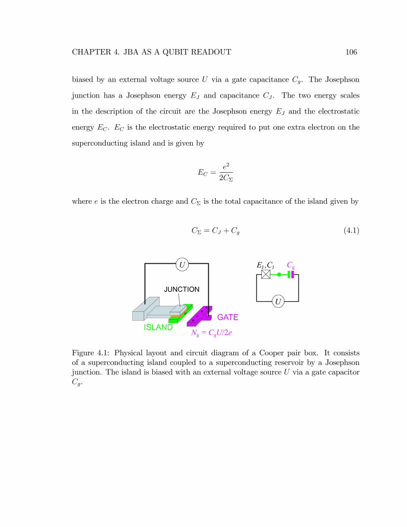
CHAPTER 4. JBA AS A QUBIT READOUT 106
biased by an external voltage source U via a gate capacitance Cg. The Josephson
junction has a Josephson energy EJ and capacitance CJ . The two energy scales
in the description of the circuit are the Josephson energy EJ and the electrostatic
energy EC . EC is the electrostatic energy required to put one extra electron on the
superconducting island and is given by
EC =e2
2C�
where e is the electron charge and C� is the total capacitance of the island given by
C� = CJ + Cg (4.1)
Figure 4.1: Physical layout and circuit diagram of a Cooper pair box. It consistsof a superconducting island coupled to a superconducting reservoir by a Josephsonjunction. The island is biased with an external voltage source U via a gate capacitorCg.
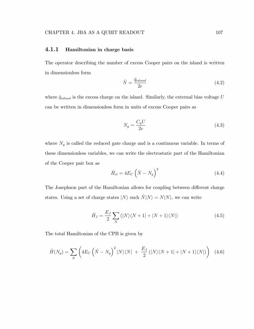
CHAPTER 4. JBA AS A QUBIT READOUT 107
4.1.1 Hamiltonian in charge basis
The operator describing the number of excess Cooper pairs on the island is written
in dimensionless form
N =qisland2e
(4.2)
where qisland is the excess charge on the island. Similarly, the external bias voltage U
can be written in dimensionless form in units of excess Cooper pairs as
Ng =CgU
2e(4.3)
where Ng is called the reduced gate charge and is a continuous variable. In terms of
these dimensionless variables, we can write the electrostatic part of the Hamiltonian
of the Cooper pair box as
Hel = 4EC
�N �Ng
�2(4.4)
The Josephson part of the Hamiltonian allows for coupling between di¤erent charge
states. Using a set of charge states jNi such N jNi = N jNi, we can write
HJ =EJ2
XN
(jNihN + 1j+ jN + 1ihN j) (4.5)
The total Hamiltonian of the CPB is given by
H(Ng) =XN
�4EC
�N �Ng
�2jNihN j + EJ
2(jNihN + 1j+ jN + 1ihN j)
�(4.6)
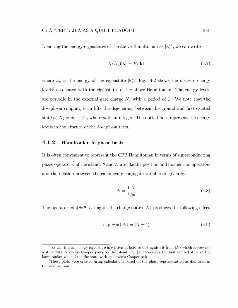
CHAPTER 4. JBA AS A QUBIT READOUT 108
Denoting the energy eigenstates of the above Hamiltonian as jki1, we can write
H(Ng)jki = Ekjki (4.7)
where Ek is the energy of the eigenstate jki. Fig. 4.2 shows the discrete energy
levels2 associated with the eigenstates of the above Hamiltonian. The energy levels
are periodic in the external gate charge Ng with a period of 1. We note that the
Josephson coupling term lifts the degeneracy between the ground and �rst excited
state at Ng = m+ 1=2, where m is an integer. The dotted lines represent the energy
levels in the absence of the Josephson term.
4.1.2 Hamiltonian in phase basis
It is often convenient to represent the CPB Hamiltonian in terms of superconducting
phase operator � of the island. � and N are like the position and momentum operators
and the relation between the canonically conjugate variables is given by
N =1
i
@
@�(4.8)
The operator exp(�i�) acting on the charge states jNi produces the following e¤ect
exp(�i�)jNi = jN � 1i (4.9)
1 jki which is an energy eigenstate is written in bold to distinguish it from jNi which representsa state with N excess Cooper pairs on the island e.g. j1i represents the �rst excited state of thehamiltonian while j1i is the state with one excess Cooper pair.
2These plots were created using calculations based on the phase representation as discussed inthe next section.

CHAPTER 4. JBA AS A QUBIT READOUT 109
Figure 4.2: Energy levels of the Cooper pair box with EJ=EC = 4:0 as a function ofgate charge Ng. The ground state and the �rst three excited states are shown. Thedotted lines correspond to the case where the Josephson coupling term is absent.
Using equations 4.8 and 4.9 we can rewrite the CPB Hamiltonian (4.6) in phase
representation as
H(Ng) = 4EC(1
i
@
@��Ng)2 � EJ cos
���
(4.10)
The advantage of using the phase representation is that the Schrödinger equation
associated with the above Hamiltonian can be solved analytically in terms of the
Mathieu functions. The Mathieu functions which are the solutions to the Mathieu
equation can be computed easily using the software package Mathematica (see [38]
for more details and Appendix B for a Mathematica notebook demonstrating the
calculations)
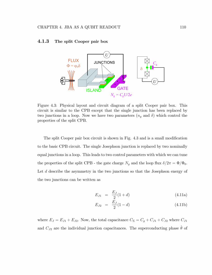
CHAPTER 4. JBA AS A QUBIT READOUT 110
4.1.3 The split Cooper pair box
Figure 4.3: Physical layout and circuit diagram of a split Cooper pair box. Thiscircuit is similar to the CPB except that the single junction has been replaced bytwo junctions in a loop. Now we have two parameters (ng and �) which control theproperties of the split CPB.
The split Cooper pair box circuit is shown in Fig. 4.3 and is a small modi�cation
to the basic CPB circuit. The single Josephson junction is replaced by two nominally
equal junctions in a loop. This leads to two control parameters with which we can tune
the properties of the split CPB - the gate charge Ng and the loop �ux �=2� = �=�0.
Let d describe the asymmetry in the two junctions so that the Josephson energy of
the two junctions can be written as
EJ1 =EJ2(1 + d) (4.11a)
EJ2 =EJ2(1� d) (4.11b)
where EJ = EJ1 + EJ2. Now, the total capacitance C� = Cg + CJ1 + CJ2 where CJ1
and CJ2 are the individual junction capacitances. The superconducting phase � of
CHAPTER 4. JBA AS A QUBIT READOUT 111
the island is now equal to the di¤erence in the phase across the individual junctions
� =�1 � �22
(4.12)
while the net phase across the two junctions is given by their sum
� = �1 + �2 (4.13)
where �1 and �2 are the individual phases across the two junctions. We will treat �
as a classical parameter � since in our measurements, the impedance across the split
junction is always kept lower than the resistance quantum h=e2 (see chapter 2 in [38]).
The external �ux � imposes a phase3 � such that � = '0� where '0 = �0=2� is the
reduced �ux quantum. So Ng and � are the two external control parameters.
The electrostatic part of the Hamiltonian remains the same as before (4.4) while
the Josephson part of the Hamiltonian can be written as
HJ = �EJ1 cos(�1)� EJ2 cos(�2) (4.14)
Using equations 4.11,4.12,4.13, and after carrying out some trigonometric manipula-
tions, we write the Josephson Hamiltonian as
HJ(�) = �EJ cos(�
2) cos(�) + dEJ sin(
�
2) sin(�) (4.15)
The above Hamiltonian reduces to the CPB Hamiltonian for d = 0 and � = 0.
For d = 0, the split Cooper pair box can be considered as a CPB with a tunable
3Assuming that the loop inductance is much smaller than Josephson inductance of the junctions

CHAPTER 4. JBA AS A QUBIT READOUT 112
Josephson energy as H(�) = �EJ cos(�=2) cos(�). The full Hamiltonian in the phase
representation for the split CPB can now be written as
H(Ng; �) = 4EC(1
i
@
@��Ng)2 � E�J(d; �) cos
�� + �(d; �)
�(4.16)
where
E�J(d; �) = EJ
r1 + d2 + (1� d2) cos(�)
2(4.17a)
tan�(d; �) = �d tan(�2) (4.17b)
The properties of the split CPB are periodic in both Ng (period 1)and � (period 2�).
In what follows, whenever a particular value of Ng or � is speci�ed, it is assumed that
the same would be true for other values which are separated by integer number of
periods e.g. Ng = N0 is the same as Ng = N0 +m where m is any integer. Similarly
� = �0 is the same as � = �0 + 2�m.
4.2 The quantronium
If we take the split CPB circuit and insert a large Josephson junction (with Josephson
energy ERJ such that ERJ >> EJ) in the loop, we get the circuit shown in Fig. 4.4.
This circuit has been nicknamed quantronium to illustrate the fact that this circuit
behaves like an arti�cial atom with the big junction being equivalent to the nucleus
and the small junctions being equivalent to electrons. This modi�cation allows one
to impose a phase di¤erence � across the split CPB junctions by means of passing a
current through the large Josephson junction, which we will call the readout junction.
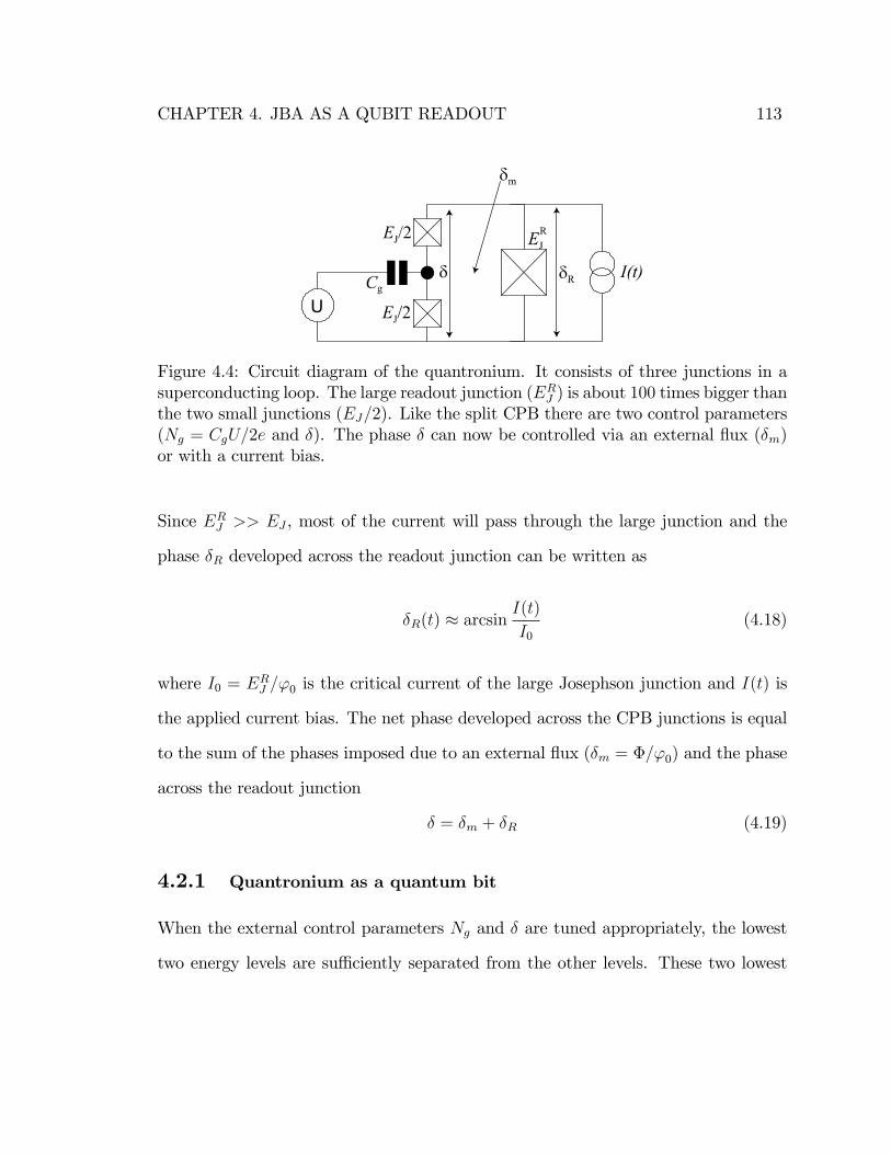
CHAPTER 4. JBA AS A QUBIT READOUT 113
Figure 4.4: Circuit diagram of the quantronium. It consists of three junctions in asuperconducting loop. The large readout junction (ERJ ) is about 100 times bigger thanthe two small junctions (EJ=2). Like the split CPB there are two control parameters(Ng = CgU=2e and �). The phase � can now be controlled via an external �ux (�m)or with a current bias.
Since ERJ >> EJ , most of the current will pass through the large junction and the
phase �R developed across the readout junction can be written as
�R(t) � arcsinI(t)
I0(4.18)
where I0 = ERJ ='0 is the critical current of the large Josephson junction and I(t) is
the applied current bias. The net phase developed across the CPB junctions is equal
to the sum of the phases imposed due to an external �ux (�m = �='0) and the phase
across the readout junction
� = �m + �R (4.19)
4.2.1 Quantronium as a quantum bit
When the external control parameters Ng and � are tuned appropriately, the lowest
two energy levels are su¢ ciently separated from the other levels. These two lowest
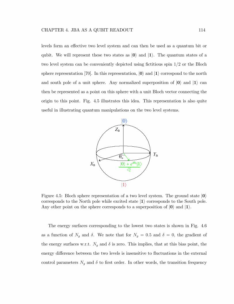
CHAPTER 4. JBA AS A QUBIT READOUT 114
levels form an e¤ective two level system and can then be used as a quantum bit or
qubit. We will represent these two states as j0i and j1i. The quantum states of a
two level system can be conveniently depicted using �ctitious spin 1=2 or the Bloch
sphere representation [70]. In this representation, j0i and j1i correspond to the north
and south pole of a unit sphere. Any normalized superposition of j0i and j1i can
then be represented as a point on this sphere with a unit Bloch vector connecting the
origin to this point. Fig. 4.5 illustrates this idea. This representation is also quite
useful in illustrating quantum manipulations on the two level systems.
Figure 4.5: Bloch sphere representation of a two level system. The ground state j0icorresponds to the North pole while excited state j1i corresponds to the South pole.Any other point on the sphere corresponds to a superposition of j0i and j1i.
The energy surfaces corresponding to the lowest two states is shown in Fig. 4.6
as a function of Ng and �. We note that for Ng = 0:5 and � = 0, the gradient of
the energy surfaces w.r.t. Ng and � is zero. This implies, that at this bias point, the
energy di¤erence between the two levels is insensitive to �uctuations in the external
control parameters Ng and � to �rst order. In other words, the transition frequency

CHAPTER 4. JBA AS A QUBIT READOUT 115
�01(Ng = 0:5; � = 0) = [E1 � E0](Ng=0:5;�=0) at this operating point is protected from
noise in Ng and � to �rst order:
�@�01@Ng
�Ng=0:5;�=0
= 0 (4.20)�@�01@�
�Ng=0:5;�=0
= 0 (4.21)
This point has been nicknamed the "sweet spot" and is the optimal point to operate
the quantronium qubit. Note that, other operating points where @�01=@(Ng; �) = 0
exist e.g. Ng = 0 and � = 0. But, the second derivative4 in charge @201�=@N2g has
a larger value at Ng = 0 when compared to its value at Ng = 0:5. Hence the best
protection from noise in Ng and � is achieved at the "sweet spot". This is important
because low frequency noise in the control parameters can cause dephasing of the
qubit [6, 40]. Unless speci�ed otherwise, all qubit manipulations are carried out at
the "sweet spot", i.e., Ng = 0:5 and � = 0.
The qubit state manipulations are carried out using techniques borrowed from
Nuclear Magnetic Resonance (NMR) experiments [71]. This involves applying a mi-
crowave frequency signal of amplitude URF and frequency �RF to the gate electrode.
This results in an additional time dependent term in the Hamiltonian 4.16 of the split
CPB
HRF = �8EC�Ng cos(2��RF t)N
where �Ng = CgURF=2e is the reduced gate voltage amplitude. Under the in�uence
of this drive, the qubit state vector precesses in a frame rotating at �RF at a frequency
4The second and higher derivatives at the sweet spot depend on the ratio EJ=EC and can betuned by adjusting sample parameters.

CHAPTER 4. JBA AS A QUBIT READOUT 116
Figure 4.6: Ground and �rst excited energy level of the quantronium as a function ofthe control parameters Ng and �. Data is shown for an EJ=EC ratio of 4: The biaspoint Ng = 0:5, � = 0 is nicknamed the sweet spot because the transition frequency�01, to �rst order, is insensitive to noise in the control parameters (Ng, �).
[38] given by
�p =
q�2Rabi + (�01 � �RF )
2 (4.22)
When this driving �eld is resonant with the qubit transition frequency, i.e., �RF = �01,
the system undergoes Rabi oscillations [72] at a rate given by
�Rabi =8EC�Ngh1jN j0i
h(4.23)
We note that �Rabi is proportional to the drive amplitude URF and to the matrix ele-
ment between the ground and �rst excited state. In the Bloch sphere representation,
this corresponds to the Bloch vector rotating from the North pole to the South pole
around the xB axis. When the qubit evolves freely (�Rabi = 0) e.g. between successive
CHAPTER 4. JBA AS A QUBIT READOUT 117
Rabi pulse, the Bloch vector precesses around the zB axis in a frame rotating at �RF ,
at a rate given by the Ramsey [73] frequency
�Ramsey = j�01 � �RF j (4.24)
Thus, a combination of driven and free evolution allows one to prepare any qubit
state on the Bloch sphere.
4.2.2 Readout strategies
We now discuss the various strategies that can be used to measure the state of the
qubit. We need to exploit some property of the quantronium which depends on its
quantum state. The control ports (gate and �ux/phase) also allow us to couple to
the qubit and measure its properties. For the quantronium qubit, there are four
quantities that can be conveniently measured to determine the state of the qubit.
These are the island charge (Qk _ @Ek=@Ng), the loop current (Ik _ @Ek=@�), the
island capacitance (Ck _ @2Ek=@N2g ) and the loop inductance (Lk _
�@2Ek=@�
2��1).
The �rst CPB based qubits employed a charge measurement technique to readout the
qubit state [4]. Measuring the charge requires an electrometer coupled to the island
of the CPB [74], but the ground and the excited state have the same average charge
when operated at the sweet spot. Hence, one has to move away from the sweet spot
(in gate charge) at the time of measurement which can lead to rapid decoherence [40].
The original quantronium qubit readout [6] was based on measuring the current in
the loop. The loop currents modi�ed the e¤ective critical current of the readout junc-
tion. This change was detected by measuring the switching of the readout junction

CHAPTER 4. JBA AS A QUBIT READOUT 118
from the superconducting state to the voltage state. This measurement also involved
moving away from the sweet spot (in phase/�ux) during the readout, because the
average current at the sweet spot was zero for both qubit states. Furthermore, the
switching of the readout junction into the voltage state led to the generation of qua-
siparticles which take a long time to recombine at low temperatures resulting in a
slow repetition rate of the experiment. The presence of quasiparticles near the qubit
can cause dissipation and lead to decoherence.
It is now well understood that dispersive measurements of the qubit state [75,
76, 77, 33], which probe the reactive part of the response of the circuit, perform
better as qubit readouts. For the CPB based qubits, this amounts to measuring the
capacitance or inductance of the qubit. This can be done by coupling the qubit to
a resonator and measuring its response under AC excitation. The measurement can
now be performed at the sweet spot as the technique probes the second derivative
(w.r.t. charge or phase) of the energy surface which has a di¤erent value for the
two qubit states even at the sweet spot. In fact, the di¤erence is maximum at this
operating point, making it ideal for measurement. Our measurement technique using
the JBA involves the measurement of the inductance by coupling the quantronium
qubit to a non-linear resonator via the phase port. Using the phase port o¤ers the
additional advantage of separating the write port (charge) from the readout port
(phase). Experiments probing the e¤ective capacitance of the CPB have also been
successfully implemented [33, 78]. It should be pointed out that the idea of an e¤ective
capacitance or inductance is valid only when the readout frequency is much smaller
than the qubit transition frequency. This condition is satis�ed for the JBA readout.
In general, one should characterize the qubit by a state dependent e¤ective impedance.
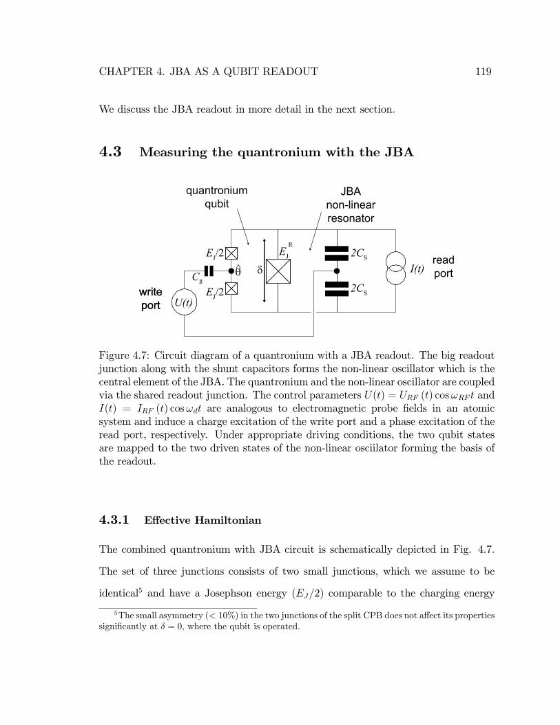
CHAPTER 4. JBA AS A QUBIT READOUT 119
We discuss the JBA readout in more detail in the next section.
4.3 Measuring the quantronium with the JBA
Figure 4.7: Circuit diagram of a quantronium with a JBA readout. The big readoutjunction along with the shunt capacitors forms the non-linear oscillator which is thecentral element of the JBA. The quantronium and the non-linear oscillator are coupledvia the shared readout junction. The control parameters U(t) = URF (t) cos!RF t andI(t) = IRF (t) cos!dt are analogous to electromagnetic probe �elds in an atomicsystem and induce a charge excitation of the write port and a phase excitation of theread port, respectively. Under appropriate driving conditions, the two qubit statesare mapped to the two driven states of the non-linear osciilator forming the basis ofthe readout.
4.3.1 E¤ective Hamiltonian
The combined quantronium with JBA circuit is schematically depicted in Fig. 4.7.
The set of three junctions consists of two small junctions, which we assume to be
identical5 and have a Josephson energy (EJ=2) comparable to the charging energy
5The small asymmetry (< 10%) in the two junctions of the split CPB does not a¤ect its propertiessigni�cantly at � = 0, where the qubit is operated.
CHAPTER 4. JBA AS A QUBIT READOUT 120
(EC) of the island between them, and a large readout junction, whose Josephson
energy (ERJ ) is approximately 100 times larger than that of each small junction.
The readout junction is shunted with capacitors (CS) to reduce its plasma frequency
to the 1 � 2 GHz range. The readout junction together with the shunt capacitors
form the non-linear resonator which is the central element of the JBA readout. The
quantronium qubit and the non-linear resonator are phase coupled via the shared
readout junction. The gauge-invariant phase di¤erence � of the island with respect
to the mid-point of the capacitance shunting the large junction is analogous to the
position of the electron relative to the nucleus of the atom, while the gauge-invariant
phase di¤erence � across the large junction is the absolute position of the nucleus.
Neglecting the dissipation induced in the transmission lines, the total Hamiltonian of
the split Cooper pair box biased at the sweet spot and coupled to a JBA resonator
is H(t) = Hbox(t) + Hres(t) with
Hbox(t) = 4EC
�N � 1
2+CgU (t)
2e
�2� EJ cos
�
2
!cos � (4.25)
Hres (t) =q2
2Cs� ERJ cos � � '0I (t) �
This Hamiltonian has been written supposing that the asymmetry between the two
small junctions is zero5, and the DC values of the o¤set gate charge and loop �ux have
been compensated to operate at the sweet spot, i.e., Ng = 1=2 and �m = 0 and hence
�R = � (see 4.19). Here, N and q=2e are the momenta conjugate to the generalized
positions � and �, respectively. The control parameters U(t) = URF (t) cos!RF t and
I(t) = IRF (t) cos!dt are analogous to electromagnetic probe �elds in an atomic
system and induce a charge excitation of the write port and a phase excitation of the

CHAPTER 4. JBA AS A QUBIT READOUT 121
read port, respectively.
If we keep these two lowest states in the Hilbert space of Hbox [40] and we express
Hres in terms of the photon creation and annihilation operators, we obtain an e¤ective
Hamiltonian
Heff =2CgU (t)
eEC�X �
EJ2�Z + ~!p (1 + ��Z) aya (4.26)
���1 +
�
4�Z
��a+ ay
�4 � f �a+ ay� I (t)where
!p =
sERJ'20CS
(4.27a)
� =EJ4ERJ
(4.27b)
� =ERC12
=1
12
(e)2
2CS(4.27c)
f = '0
�2ERCERJ
�1=4(4.27d)
The photon annihilation operator a is related to � by
� =a+ ay
(ERJ =2ERC )
1=4(4.28)
which represents the decomposition of the gauge-invariant phase di¤erence into anni-
hilation and creation operators of the �plasma�mode whose bare frequency is !p. The
operators �X and �Z are the Pauli spin operators and ERC = e2= (2CS) is the single
electron charging energy of the readout junction. In this e¤ective Hamiltonian, the
expansion of cos � is carried out only to the �rst anharmonic term, which describes
CHAPTER 4. JBA AS A QUBIT READOUT 122
the non-linear resonator dynamics with su¢ cient accuracy for a bifurcation readout
(see chapter 2).
Let us describe the role of each term in equation 4.26. The �rst term describes the
in�uence on the qubit of the charge port drive which is used to manipulate its state.
The second term describes the free evolution of the qubit at the Larmor frequency
!01 = EJ=~. We have supposed here that the ratio EJ=EC is su¢ ciently small that
corrections to the Larmor frequency involving EC are small. To model the behavior
of qubit samples with an appreciable EJ=EC ratio, we would keep higher order terms,
yielding renormalized values of the coe¢ cients in equation 4.26. The third term
describes the dominant coupling between the qubit and the resonator. Note that this
term commutes with the Hamiltonian of the qubit when U = 0, o¤ering the possibility
of quantum non-demolition measurements6 (see chapter 6 for more details). The
fourth term describes a decrease in the frequency of the resonator when its photon
population increases (chapter 2). Finally, the �fth term describes the excitation of
the resonator by the drive current applied through the phase port. When the drive
current is increased while its frequency is su¢ ciently below !p the system becomes
metastable with two possible dynamical states with di¤erent oscillation amplitudes
(chapter 2). We exploit this bistability for our readout, which we describe in the next
section.
4.3.2 Measurement protocol
It is clear from the Hamiltonian (4.26) above that the dynamics of the non-linear
resonator depend on the value �Z = �1 corresponding to the state of the qubit.
6This is strictly true in the limit of zero asymmetry d = 0. For �nite values of d, corrections tothe QND fraction of order d2 exists [79].
CHAPTER 4. JBA AS A QUBIT READOUT 123
In particular, the small oscillation �plasma�frequency !e�p = !p (1� �) varies with
the qubit state. We probe the nonlinear resonator by sending down the phase port
transmission line a microwave pulse with carrier frequency !d = !p ��!, such that
the detuning �! >p3
2Q!p where Q is the quality factor of the plasma resonance
(chapter 2). In our circuit, the damping of the plasma resonance arises from the
characteristic transmission line impedance Zc = 50 and thus Q = ZcC!p ' 10�20.
For this value of detuning, when ramping up the drive current IRF the resonator
switches from one dynamical state to another when
IRF > I+B
�!d; !
e�p
�(4.29)
where I+B is the bifurcation current (equation 2.16). Therefore, by choosing the max-
imum pulse amplitude
I+B [!d; !p (1� �)] < ImaxRF < I+B [!d; !p (1 + �)] (4.30)
we can determine, by measuring if the resonator has switched or not, whether the
qubit was in state j0i or j1i.
The dynamical states of the resonator di¤er in both the amplitude and phase
of the forced oscillations at frequency !d. In this work, we have chosen to use a
re�ectometry setup in which all the information about the resonator state is carried
by the re�ected drive signal phase �. This last property occurs because the probed
circuit is not intrinsically dissipative (in absence of quasi-particles, which is very well
realized in our measurements) and the power re�ected from the chip is equal to the
incident power in steady state.
CHAPTER 4. JBA AS A QUBIT READOUT 124
As explained in chapter 2, a further advantage of the non-linear resonator is that
the switching is strongly hysteretic. Once a switching event has occurred we can de-
crease the drive current IRF to a value which, while much smaller than I+B [!d; !p (1� �)],
is still higher than the reverse bifurcation �retrapping� current I�B . This latching
property conserves the information about the qubit state acquired during a small
time interval �m in the resonator and allows us to probe the re�ected phase � during
a time typically longer than �m. This helps in determining the re�ected signal phase
with much higher accuracy (see section 3.3) without being a¤ected by any subsequent
evolution of the qubit.
4.3.3 E¤ective critical current
The last two subsections gave us a simple picture to understand the coupling between
the qubit and the JBA. The calculation was carried out in the limit EJ=EC << 1.
But in order to make accurate predictions for the performance of the JBA as a qubit
readout, we will use the full expressions for the loop currents computed in the phase
representation. We saw in chapter 2 that the JBA converts changes in the critical
current of the Josephson junction to changes in switching probability, i.e., the JBA
ampli�es changes in critical current. Hence, it is convenient to consider the changes
in e¤ective critical current of the qubit+JBA system as the main signal of interest7.
This can then be converted to changes in switching probability once the parameters
of the JBA are known (see section 2.3.3).
We need to compute the loop currents of the quantronium as a function of � in
order to determine its e¤ect on the critical current of the Josephson junction, i.e., we
7This is equivalent to considering the changes in e¤ective inductance (LJ _ I�10 ) but is compu-tationally more convenient.
CHAPTER 4. JBA AS A QUBIT READOUT 125
need to calculate the current-phase relationship for the quantronium. For the readout
junction, this is given by the standard Josephson relationship I(�) = I0 sin �. For DC
experiments, the critical current is the maximum current that can be passed before
the junction switches into its voltage state and is given by I (� = �=2) = I0. Here, we
will de�ne the e¤ective critical current as the slope of the current-phase relationship
at � = 0.
Ieff0 =
����@I(�)@�
�����=0
(4.31)
This is related to the fact that we are essentially probing the inductance of the
quantronium which is proportional to the inverse of this slope.
LeffJ = '0
�����@I(�)@�
�����=0
��1(4.32)
For the bare readout junction, Ieff0 = I0, but this not true for the quantronium which
typically has a non-sinusoidal current-phase relationship. The loop currents in the
quantronium are given by [38]
ik (Ng; �) =1
'0
@Ek(Ng; �)
@�(4.33)
Then from equation 4.31, we can write the e¤ective critical current for the quantro-
nium as
ieffk (Ng; �m) =1
'0
@2Ek(Ng; � = �m)
@�2(4.34)
where �m takes into account an external �ux bias. The above expression can be
computed in terms of the Mathieu functions (Appendix B). Fig. 4.8 shows a plot of
the loop currents in the ground and excited state at Ng = 0:5. The parameters used

CHAPTER 4. JBA AS A QUBIT READOUT 126
correspond to the four qubit samples whose data is presented in chapters 5 and 6.
Figure 4.8: Loop currents for the ground and �rst excited state of the quantroniumqubit are plotted as a function of phase � (for Ng = 0:5). Theoretical curves areshown for four di¤erent qubit samples. One can observe how the shape of the loopcurrents depends on the EJ=EC ratio.
We note that the current-phase relationship for the quantronium depends on the
EJ=EC ratio quite strongly. For small values of EJ=EC , the loop currents have oppo-
site signs for the ground and excited states, but for larger values, they have the same
sign. However, the slopes at � = 0 are always di¤erent allowing one to discriminate
between the two states. The ground state properties of the quantronium are often the
�rst quantities to be measured in an experiment. We plot in Fig. 4.9 the variation
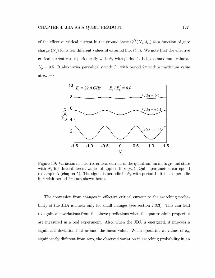
CHAPTER 4. JBA AS A QUBIT READOUT 127
of the e¤ective critical current in the ground state ieff0 (Ng; �m) as a function of gate
charge (Ng) for a few di¤erent values of external �ux (�m). We note that the e¤ective
critical current varies periodically with Ng with period 1. It has a maximum value at
Ng = 0:5. It also varies periodically with �m with period 2� with a maximum value
at �m = 0.
Figure 4.9: Variation in e¤ective critical current of the quantronium in its ground statewith Ng for three di¤erent values of applied �ux (�m). Qubit parameters correpondto sample A (chapter 5). The signal is periodic in Ng with period 1. It is also periodicin � with period 2� (not shown here).
The conversion from changes in e¤ective critical current to the switching proba-
bility of the JBA is linear only for small changes (see section 2.3.3). This can lead
to signi�cant variations from the above predictions when the quantronium properties
are measured in a real experiment. Also, when the JBA is energized, it imposes a
signi�cant deviation in � around the mean value. When operating at values of �m
signi�cantly di¤erent from zero, the observed variation in switching probability in an
CHAPTER 4. JBA AS A QUBIT READOUT 128
experiment can vary signi�cantly from the above prediction. The qubit can also Zener
tunnel between the ground and excited state during measurements near �m = 0:5,
which can a¤ect the switching probability. In order to fully understand the e¤ect of
the quantronium on the JBA, we carried out classical numerical simulations of the
JBA but used the modi�ed current-phase relations to fully incorporate the e¤ect of
the quantronium. This is discussed in more detail in the next section. Nevertheless,
the e¤ective critical current discussed above provides a convenient way to predict the
expected signal in a qubit measurement using simple analytical formulae and without
resorting to time consuming numerical simulations.
4.3.4 Qubit readout optimization
We now consider the problem of choosing the parameters for the quantronium and
JBA to achieve the best possible qubit readout. As discussed in chapter 3, the JBA
parameters are dictated by the requirement that !p=2� � 1� 2 GHz8, Q � 20 and
R = 50 . This leads to a junction critical current I0 � 1 �A and shunt capacitance
CS � 30 pF. For the quantronium, we are looking to maximize the change in e¤ective
critical current (�ieff01 ) between the two qubit states. This is entirely determined by
the choice of EJ and EC . In order to achieve robust microwave design and signal
manipulation, it is better to keep the qubit Larmor frequency �01 < 20 GHz. The
qubit Larmor frequency also depends on EJ and EC . Once �01 is �xed, the other free
parameter is the ratio EJ=EC . It can be shown that the critical current variation
�ieff01 / �01. Fig. 4.10 shows the variation of �ieff01 =�01 with EJ=EC .
8This is not a fundamental requirement but only constrained by our choice of experimentalsetup. We have succesfully operated the JBA up to 4:5 GHz and to about 10 GHz with geometricresonators (CBA).

CHAPTER 4. JBA AS A QUBIT READOUT 129
Figure 4.10: Di¤erence in e¤ective critical current (�ieff01 ) between the ground andexcited state of the quantronium as a function of EJ=EC . �i
eff01 is larger for larger
values of �01. As EJ=EC ratio increases beyond a value of 10, �ieff01 tends to saturate.
We note that �ieff01 =�01 has two asymptotic values for small and large values of
EJ=EC . It starts out with a value of around 0:5 at low values of EJ=EC . It then
decreases with increasing values of EJ=EC but tends to saturate to value of around 0:3
for EJ=EC > 10. This is related to the fact that the Larmor frequency �01 �! EJ for
EJ=EC << 1 while �01 �!p8EJEC for EJ=EC >> 1. Also, the loop currents have
opposite signs for EJ=EC << 1 resulting in a bigger signal while the loop currents
tend to have the same sign for EJ=EC >> 1. As discussed earlier in this chapter,
the sensitivity to low frequency charge noise decreases dramatically with increasing
EJ=EC and typically EJ=EC > 4 is used. The experiments presented in the next
two chapter were carried out on four samples with EJ=EC ratios of 6, 2:7, 17:5, and

CHAPTER 4. JBA AS A QUBIT READOUT 130
1:8. From the above plot, we can estimate that for values of EJ=EC > 10, we get a
critical current variation (�ieff01 ) of about 0:3 nA per GHz for the Larmor frequency.
If we have �01 = 20 GHz, we can get a critical current variation between 6 and 10 nA
depending on the EJ=EC ratio. In section 4.4, we will use these numbers to predict
the performance of the JBA as a qubit readout.
As discussed above, the value of �ieff01 is limited to a certain range due to experi-
mental constraints. In order to enhance this signal, we developed a new circuit which
uses two readout junction in series to increase the coupling between the JBA and the
quantronium. The two readout junctions now have twice the original value of ERJ
which results in the double junction JBA (DJBA) having the same plasma frequency
as the single junction JBA. This circuit e¤ectively doubles the coupling and the hence
the e¤ective change in critical current (�ieff01 ). Numerical simulations with the DJBA
con�rm this e¤ect (section 4.4).
4.3.5 Qubit readout performance
We now de�ne a few quantities which are useful for gauging the performance of a
qubit readout. The �rst quantity is the gain or transfer function of the detector. In
the case of JBA, the relevant quantity is the change in switching probability (�Pswitch)
per unit change in critical current of the junction (�I0). We will denote this quantity
by
GJBA =�Pswitch�I0
: (4.35)
This quantity only depends on the parameters of the JBA (including pulse parameters
and temperature) and does not depend on the qubit parameters. It characterizes the
sensitivity of the detector. As mentioned earlier in this section, equation 4.35 is valid
CHAPTER 4. JBA AS A QUBIT READOUT 131
only for small changes in critical current and the gain drops as �I0 increases. For
a qubit readout, the qubit parameters set the value of �I0. So the gain can be
computed for the given value of �I0.
The next quantity characterizes a given qubit readout system. Once the parame-
ters of the qubit are known, we can calculate �I0 = �ieff01 and hence the expected
�Pswitch. We call this quantity the discrimination power and is given by
�dp = �ieff01 GJBA
��ieff01
�(4.36)
where we have written gain GJBA as a function of �ieff01 to emphasize that the gain
has been calculated for a particular value of �ieff01 . This quantity tells us the expected
performance of the given qubit readout system. While setting up an experiment, we
will try to adjust the parameters so that the value of �dp is as close to 1:0 as possible.
We will compute this number for a few systems in the next section.
The next quantity called contrast (�c) is the actual �Pswitch observed in a qubit
readout experiment. This is the actual performance of the qubit readout achieved in
a given experiment. This incorporates all possible problems in the qubit as well as
the readout.
The three quantities GJBA, �dp, and �c allow us to gauge the anticipated and the
actual performance of the qubit readout system. There are two more quantities which
are sometimes useful to characterize a qubit readout. The �rst one is called the readout
�delity (�f) and takes into account imperfections in the qubit e.g. �nite qubit lifetime
and state preparation of the qubit. These imperfections can reduce the contrast in an
experiment and the readout �delity allows us to isolate the qubit/technical problems
CHAPTER 4. JBA AS A QUBIT READOUT 132
from the detector performance. Note that the readout �delity still includes any back-
action e¤ects which could be present during a measurement. The last quantity is
called visibility and is given by
�v =�c�dp
(4.37)
This quantity compares the achieved performance (�c) to the anticipated performance
(�dp) of a qubit readout system. In a typical experiment, the quantities �dp,�f and �c
line up as follows
�dp � �f � �c (4.38)
though ideally we would like �dp = �f = �c = 1:0. Chapter 6 discusses experimental
results which help us identify some of the problems which results in a reduced contrast.
4.4 Numerical simulations
We will now brie�y describe the numerical simulations that were carried out to char-
acterize the performance of the JBA as a qubit readout. The equation of motion
for the JBA was given in equation 2.1. In order to incorporate the e¤ect of the
quantronium, we just add a term corresponding to the current-phase relationship of
the quantronium (4.33)
CJ'0d2�(t)
dt2+'0R
d�(t)
dt+ I0 sin �(t) + ik (Ng; �m + �) = I(t) + IN (t) (4.39)
where k, Ng and �m are constants for a given problem and determine the qubit state,
gate bias and �ux bias respectively. The loop current function ik (Ng; �m + �), is
incorporated in the numerical simulation by storing a sampled version (calculated in

CHAPTER 4. JBA AS A QUBIT READOUT 133
Mathematica) in an array for given values of k, Ng and �m. I(t) is the RF current drive
and IN (t) is the Johnson noise current corresponding to a given temperature. A C++
code solves the above equation (in reduced units) using the 4th order Runge-Kutta
method. The details of the implementation are given in Appendix C.
Each numerical experiment involves simulating the above equation for a given set
of parameters. The simulator outputs � (t) from which we can determine the state of
the JBA at the end of a particular numerical experiment. By repeating the experiment
many times one can compute the switching probability Pswitch. One can then study
the variation of Pswitch as a function of the control parameters like drive amplitude
and temperature. In Fig. 4.11 we show plots of the switching probability curves or S-
curves which plot the variation of Pswitch with drive amplitude. Numerically simulated
S-curve data9 is shown for typical qubit parameters with�ieff01 = 4:5 nA (corresponds
to Sample B, see chapter 5) for both the ground and the excited state. A simulation
temperature of T = 80 mK was used, while !p=2� = 1:7 GHz and !d=2� = 1:55 GHz
for the JBA. The value of temperature (T ) used for this simulation is our best guess for
the e¤ective temperature10 which was determined through other measurements (not
described here). This allows us to determine the expected discrimination power (�dp)
which is computed by taking the maximum of the di¤erence between the S-curves
corresponding to the two qubit states. The discrimination power tells us how good
the JBA will perform as a qubit readout e.g. �dp = 0:7 implies that the JBA should
measure the qubit state correctly 70% of the times. The panels (a) and (b) compare
9The actual equation used in the numerical simulation is slightly di¤erent from equation 4.39to incorporate e¤ects of stray parameters in the circuit. See section 3.2.1 and Appendix C for moredetails.
10The e¤ective temperature of the JBA when T << ~!p, is given by Teff = ~!p= (2kB) (chapter7&8). It could be higher if the microwave lines connected to the JBA are not su¢ ciently �ltered.

CHAPTER 4. JBA AS A QUBIT READOUT 134
Figure 4.11: Switching probability curves computed using numerical simulations ofthe quantronium+JBA circuit. The e¤ect of the quantronium was incorporated byincluding the current-phase relation of the quantronium. Data is shown for typicalqubit parameters with �ieff01 = 4:5 nA (corresponds to Sample B, see chapter 5).A simulation temperature of T = 80 mK was used, while !p=2� = 1:7 GHz and!d=2� = 1:55 GHz for the JBA. Panel (a) shows the case for a single junction JBAwhile panel (b) is for the double junction JBA and we see an improvement in �dp from0.7 to 0.9. An interesting feature to note is that the width of the S-curves (in unitsof current) is roughly the same for the two cases but the shift is double in panel (b).This is a consequence of enhanced (roughly double) coupling to the quantronium inthe double junction JBA. Also note that the typical values of ImaxRF are also doublein panel (b) due to the fact that the critical currents of the individual junctions aredoubled to keep the same !p.
CHAPTER 4. JBA AS A QUBIT READOUT 135
results for the single junction JBA with the double junction JBA which provides
enhanced coupling to the quantronium and hence higher discrimination power.
The ultimate goal is to get �dp = 1:0 (and �c = 1:0), but a readout with �dp < 1
is still usable. It just means that the experiment has to be repeated several times in
order to determine the qubit state accurately. As discussed in the previous section,
discrimination power mainly depends on two quantities. The �rst is the e¤ective
change in critical current (�ieff01 ) when the qubit state changes. �ieff01 depends on
EJ and EC and determines the shift in the S-curves. The second is the e¤ective
temperature of the JBA which determines the width of the S-curves (sections 2.3.3
and 3.3.2). We will see in chapters 7 and 8 that the e¤ective temperature of the
JBA has a lower bound and is given by Teff = ~!p= (2kB). In order to get closer to
�dp; �c = 1:0, one can use tricks like enhanced coupling using the DJBA. In certain
cases, it is possible to access the second excited state (j2i) by sending a microwave
pulse at frequency �12 to the gate port, just before the measurement. For certain
range of parameters, �ieff02 is bigger than �ieff01 and can provide an improvement in
contrast. The next two chapters discuss experimental results of measurements carried
out on the quantronium qubit using the JBA.

Chapter 5
Qubit coherence measurements
In this chapter, we will describe the measurements that were carried out on the
quantronium qubit (see chapter 4) using the JBA, to probe its coherence properties.
The experiments were carried out in a dilution refrigerator with a base temperature of
12 mK. We will �rst discuss the new experimental setup for the qubit measurements.
The measurements characterizing the ground state of the split Cooper pair box will
then be discussed. This will be followed by the discussion of the spectroscopic mea-
surements of the excited state. We will then describe the time domain measurements
which characterize the coherence properties of the qubit. Finally, we will talk about
the �delity of the JBA readout.
5.1 Measurement setup
The principle of our experiment is schematically depicted in Fig. 5.1 and is based, as
discussed in the previous chapter, on the quantronium qubit, a three junction circuit
which is analogous to a one-dimensional atom. The set of three junctions consists of
136
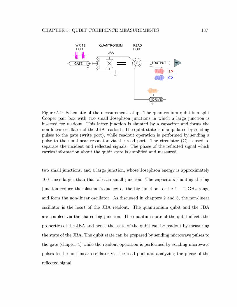
CHAPTER 5. QUBIT COHERENCE MEASUREMENTS 137
Figure 5.1: Schematic of the measurement setup. The quantronium qubit is a splitCooper pair box with two small Josephson junctions in which a large junction isinserted for readout. This latter junction is shunted by a capacitor and forms thenon-linear oscillator of the JBA readout. The qubit state is manipulated by sendingpulses to the gate (write port), while readout operation is performed by sending apulse to the non-linear resonator via the read port. The circulator (C) is used toseparate the incident and re�ected signals. The phase of the re�ected signal whichcarries information about the qubit state is ampli�ed and measured.
two small junctions, and a large junction, whose Josephson energy is approximately
100 times larger than that of each small junction. The capacitors shunting the big
junction reduce the plasma frequency of the big junction to the 1 � 2 GHz range
and form the non-linear oscillator. As discussed in chapters 2 and 3, the non-linear
oscillator is the heart of the JBA readout. The quantronium qubit and the JBA
are coupled via the shared big junction. The quantum state of the qubit a¤ects the
properties of the JBA and hence the state of the qubit can be readout by measuring
the state of the JBA. The qubit state can be prepared by sending microwave pulses to
the gate (chapter 4) while the readout operation is performed by sending microwave
pulses to the non-linear oscillator via the read port and analyzing the phase of the
re�ected signal.

CHAPTER 5. QUBIT COHERENCE MEASUREMENTS 138
Figure 5.2: Fridge setup for qubit measurements. There are three microwave linesand one DC line. The readout injection and the RF gate line are attenuated and�ltered whle the readout return line has isolators and lossy �lters. The DC gateline has a voltage divider and copper powder �lters. Typical values of attenuatorsused are indicated. They were varied between di¤erent experiments depending on theparameters being optimized.
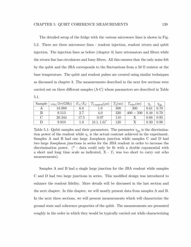
CHAPTER 5. QUBIT COHERENCE MEASUREMENTS 139
The detailed setup of the fridge with the various microwave lines is shown in Fig.
5.2. There are three microwave lines - readout injection, readout return and qubit
injection. The injection lines as before (chapter 3) have attenuators and �lters while
the return line has circulators and lossy �lters. All this ensures that the only noise felt
by the qubit and the JBA corresponds to the �uctuations from a 50 resistor at the
base temperature. The qubit and readout pulses are created using similar techniques
as discussed in chapter 3. The measurements described in the next few sections were
carried out on three di¤erent samples (A-C) whose parameters are described in Table
5.1.
Sample !01=2�(GHz) EJ=EC T1;typical(�s) T2(ns) Techo(ns) �c �dpA 18:989 6:0 1:0 300 300 0:61 0:70B 9:513 2:7 4:0 320 400� 500 0:48 0:70C 20:344 17:5 0:07 110 X 0:68 0:95
D 9:910 1:8 (0:1; 1:0)* 120 X 0:30 0:90
Table 5.1: Qubit samples and their parameters. The parameter �dp is the discrimina-tion power of the readout while �c is the actual contrast achieved in the experiment.Samples A and B had one large Josephson junction while samples C and D hadtwo large Josephson junctions in series for the JBA readout in order to increase thediscrimination power. (* - data could only be �t with a double exponential witha short and long time scale as indicated, X - T1 was too short to carry out echomeasurements).
Samples A and B had a single large junction for the JBA readout while samples
C and D had two large junctions in series. This modi�ed design was introduced to
enhance the readout �delity. More details will be discussed in the last section and
the next chapter. In this chapter, we will mostly present data from samples A and B.
In the next three sections, we will present measurements which will characterize the
ground state and coherence properties of the qubit. The measurements are presented
roughly in the order in which they would be typically carried out while characterizing
CHAPTER 5. QUBIT COHERENCE MEASUREMENTS 140
a qubit. This gives us a �avour of the sequence of operations involved during a typical
experiment.
5.2 Ground state characterization
The �rst step in a qubit measurement is to characterize the ground state properties
of the qubit as a function of the bias parameters (gate and �ux). But before one
can carry out any measurements, it is necessary to characterize the JBA readout, the
procedure for which was described in chapter 3. We identify an operating frequency
and the pulse parameters for the JBA readout. These parameters are often modi�ed
later to optimize the signal to noise ratio and the readout �delity. Once the readout
is ready, the only quantity that is monitored is the switching probability of the JBA
which is the main output signal of any measurement.
As discussed in the previous chapter, the properties of the quantronium are peri-
odic functions of the gate charge (Ng) and loop �ux (�l). At low enough temperature
(kBT << ~!01) and in the absence of any microwave irradiation on the qubit, the
qubit stays predominantly in its ground state due to the �nite lifetime of the excited
state. We monitor the switching probability of the JBA as a function of gate and
�ux bias and the result (sample A) is shown Fig. 5.3. Each trace is a plot of the
switching probability (Pswitch) as a function of the gate voltage for a given value of
�ux. The readout bias is adjusted at every value of �ux bias to give a mean value
of Pswitch = 0:5. As is expected, the modulations in Pswitch increase as the �ux bias
deviates from zero (or integer �ux quantum). The modulation magnitude at zero �ux
depends on the EJ and EC values of the Cooper-pair transistor. For large ratios of
EJ=EC , this modulation can be quite small and di¢ cult to measure. In that regard,

CHAPTER 5. QUBIT COHERENCE MEASUREMENTS 141
Figure 5.3: Switching probability v.s. DC gate voltage for di¤erent values for bias�ux. Data (sample A) shows the periodic nature of the ground state properties ofthe quantronium. As discussed in chapter 4, the JBA probes the e¤ective criticalcurrent of the quantronium which varies periodically with gate charge Ng with period1. By noting that the period in gate voltage is 15 mV = 2e=Cg, we can extract thegate capacitance of this sample Cg =21 aF. The magnitude of the modulation alsochanges with the bias �ux as expected for the quantronium.
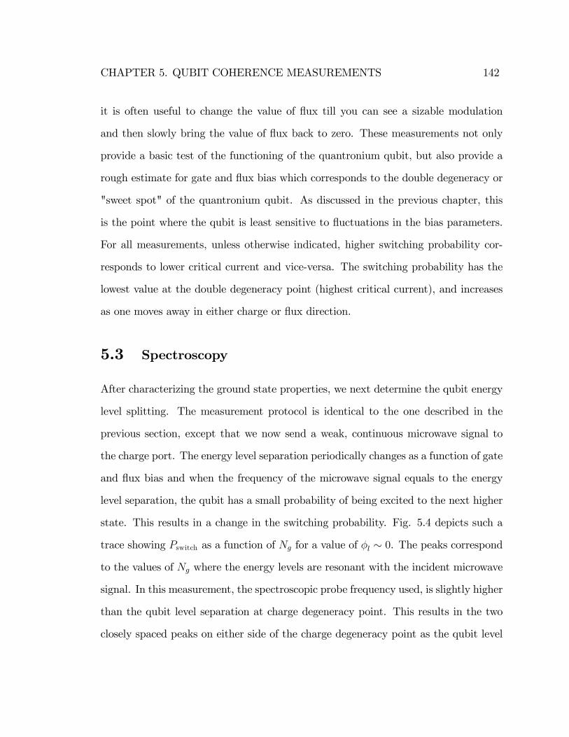
CHAPTER 5. QUBIT COHERENCE MEASUREMENTS 142
it is often useful to change the value of �ux till you can see a sizable modulation
and then slowly bring the value of �ux back to zero. These measurements not only
provide a basic test of the functioning of the quantronium qubit, but also provide a
rough estimate for gate and �ux bias which corresponds to the double degeneracy or
"sweet spot" of the quantronium qubit. As discussed in the previous chapter, this
is the point where the qubit is least sensitive to �uctuations in the bias parameters.
For all measurements, unless otherwise indicated, higher switching probability cor-
responds to lower critical current and vice-versa. The switching probability has the
lowest value at the double degeneracy point (highest critical current), and increases
as one moves away in either charge or �ux direction.
5.3 Spectroscopy
After characterizing the ground state properties, we next determine the qubit energy
level splitting. The measurement protocol is identical to the one described in the
previous section, except that we now send a weak, continuous microwave signal to
the charge port. The energy level separation periodically changes as a function of gate
and �ux bias and when the frequency of the microwave signal equals to the energy
level separation, the qubit has a small probability of being excited to the next higher
state. This results in a change in the switching probability. Fig. 5.4 depicts such a
trace showing Pswitch as a function of Ng for a value of �l � 0. The peaks correspond
to the values of Ng where the energy levels are resonant with the incident microwave
signal. In this measurement, the spectroscopic probe frequency used, is slightly higher
than the qubit level separation at charge degeneracy point. This results in the two
closely spaced peaks on either side of the charge degeneracy point as the qubit level

CHAPTER 5. QUBIT COHERENCE MEASUREMENTS 143
splitting increases as one moves away from the charge degeneracy point.
Figure 5.4: Spectrocopic peaks for sample A. The qubit is irradiated with a continuousmicrowave signal while the gate bias is swept. The switching probably shows the usualgate modulation but now has additional peaks at certain values of gate bias whenthe qubit level spacing becomes resonant with the incident microwave radiation. Themicrowave frequency used here is slightly larger than the Larmor frequency at thecharge degeneracy point.
We can then map the variation of the qubit level splitting as a function of gate
charge by using di¤erent probe frequencies. This data for sample A is shown in Fig.
5.5 and allows us to determine the EJ and EC values for the qubit. The brighter
regions correspond to the qubit being excited by the incident microwaves. The light
blue curve is the theoretical �t for the variation of qubit transition frequency with
gate charge. Sample A had a EJ=EC ratio of about 6 and the curvature of the
energy bands with charge is not too high even at Ng = 0. This is evident from the
spectroscopy data as shown in Fig. 5.5 We were able to carry out coherent operations
on the qubit at both Ng = 0:5 and Ng = 0 for sample A.
Now we know the approximate value of the Larmor frequency !01. We then
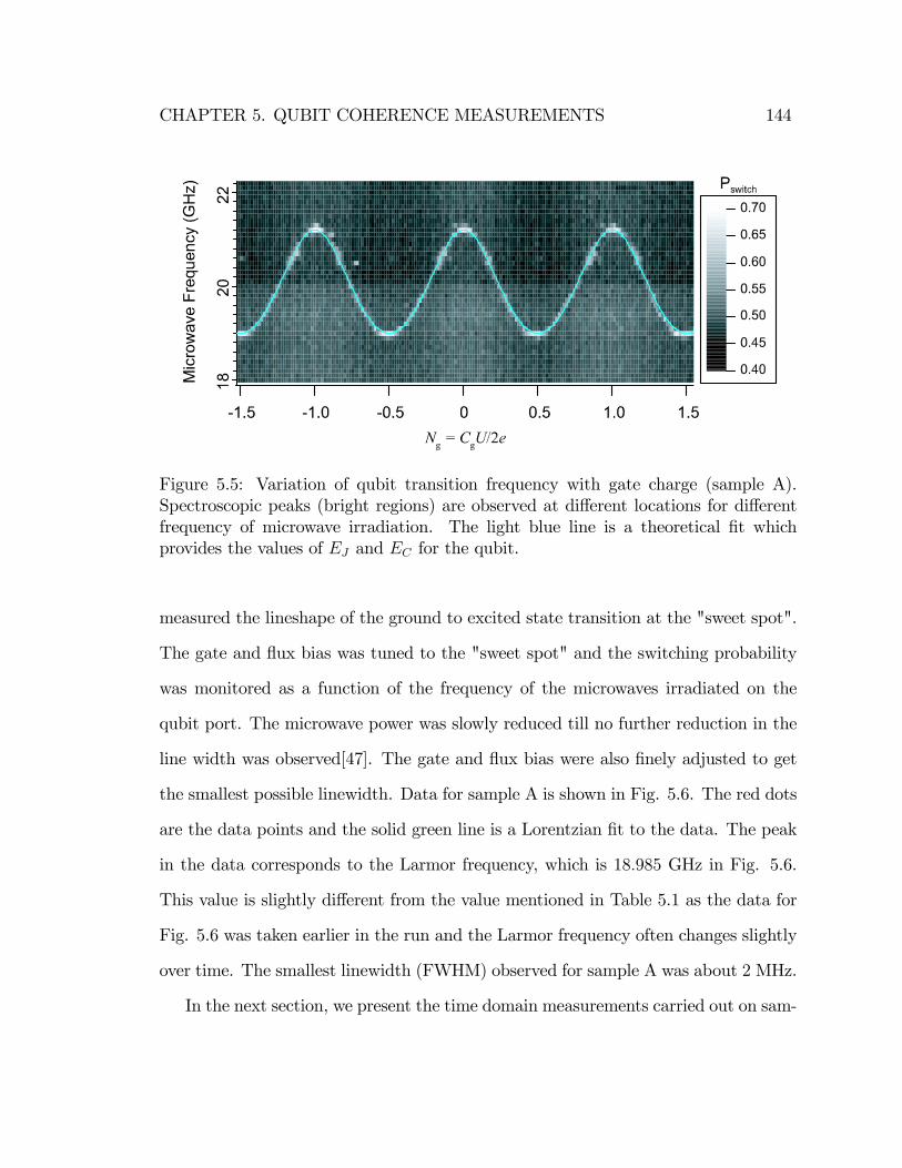
CHAPTER 5. QUBIT COHERENCE MEASUREMENTS 144
Figure 5.5: Variation of qubit transition frequency with gate charge (sample A).Spectroscopic peaks (bright regions) are observed at di¤erent locations for di¤erentfrequency of microwave irradiation. The light blue line is a theoretical �t whichprovides the values of EJ and EC for the qubit.
measured the lineshape of the ground to excited state transition at the "sweet spot".
The gate and �ux bias was tuned to the "sweet spot" and the switching probability
was monitored as a function of the frequency of the microwaves irradiated on the
qubit port. The microwave power was slowly reduced till no further reduction in the
line width was observed[47]. The gate and �ux bias were also �nely adjusted to get
the smallest possible linewidth. Data for sample A is shown in Fig. 5.6. The red dots
are the data points and the solid green line is a Lorentzian �t to the data. The peak
in the data corresponds to the Larmor frequency, which is 18:985 GHz in Fig. 5.6.
This value is slightly di¤erent from the value mentioned in Table 5.1 as the data for
Fig. 5.6 was taken earlier in the run and the Larmor frequency often changes slightly
over time. The smallest linewidth (FWHM) observed for sample A was about 2MHz.
In the next section, we present the time domain measurements carried out on sam-
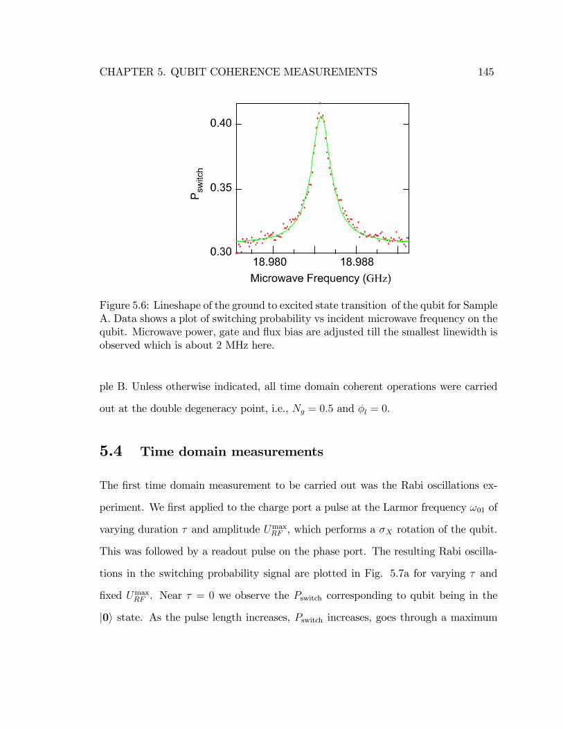
CHAPTER 5. QUBIT COHERENCE MEASUREMENTS 145
Figure 5.6: Lineshape of the ground to excited state transition of the qubit for SampleA. Data shows a plot of switching probability vs incident microwave frequency on thequbit. Microwave power, gate and �ux bias are adjusted till the smallest linewidth isobserved which is about 2 MHz here.
ple B. Unless otherwise indicated, all time domain coherent operations were carried
out at the double degeneracy point, i.e., Ng = 0:5 and �l = 0.
5.4 Time domain measurements
The �rst time domain measurement to be carried out was the Rabi oscillations ex-
periment. We �rst applied to the charge port a pulse at the Larmor frequency !01 of
varying duration � and amplitude UmaxRF , which performs a �X rotation of the qubit.
This was followed by a readout pulse on the phase port. The resulting Rabi oscilla-
tions in the switching probability signal are plotted in Fig. 5.7a for varying � and
�xed UmaxRF . Near � = 0 we observe the Pswitch corresponding to qubit being in the
j0i state. As the pulse length increases, Pswitch increases, goes through a maximum
CHAPTER 5. QUBIT COHERENCE MEASUREMENTS 146
Figure 5.7: a) Rabi oscillations of the switching probability of qubit sample B asa function of the duration � of a square pulse applied on the gate with maximumamplitude UmaxRF = 0:12mV. Solid green curve is an exponentially decaying sinusoidal�t with eT2 = 1:6�s. Total acquisition time is 3 minutes and the repetition rate is16�s, set by T1 (see below). b) Rabi oscillation frequency (�Rabi) measured in (a) asa function of UmaxRF . Green line represents the expected linear dependence.

CHAPTER 5. QUBIT COHERENCE MEASUREMENTS 147
where the qubit is purely in the j1i state, de�ning at this point the length of a � pulse.
The switching probability then decreases back to the j0i state value, indicating a full
2� rotation of the Bloch vector. This pattern repeats itself but with diminishing
contrast. The decay time eT2 is in the range 0:8 � 1:7�s depending on the sampleand precise biasing condition. The Rabi oscillation frequency �Rabi is plotted as a
function of UmaxRF in Fig. 5.7b. A linear dependence of �Rabi with UmaxRF is observed,
in agreement with theory. The shortest � pulse we generated was 2 ns long, and was
used in the echo experiments described below.
Having calibrated the � pulse, we then performed a qubit energy relaxation mea-
surement by introducing a waiting time tw between the � pulse and the readout pulse.
The decay of Pswitch with tw, shown in Fig. 5.8, is well �tted by a single exponential,
de�ning T1. For sample A, T1 was in the range 1:0� 1:3�s, and for sample B, T1 was
between 2:5�5�s. The values of T1 obtained with our dispersive readout are compa-
rable with the results of Vion et al. [6], and are signi�cantly shorter than the values
expected from coupling to a well thermalized 50 microwave environment shunting
the qubit. The loss mechanisms giving rise to the observed energy relaxation are not
understood at this time.
Following measurements of the qubit energy relaxation, we performed a Ramsey
fringe experiment to determine the phase coherence of the qubit. In this experiment,
two �=2 pulses were applied to the charge port of the qubit at a frequency 10�20MHz
detuned from !01 followed by a readout pulse on the phase port. A free evolution
time �t was introduced between the two �=2 pulses. In Fig. 5.9, Pswitch is plotted
as a function of �t. In the Ramsey sequence, the �rst �=2 pulse tips the Bloch
vector from the north pole to the equatorial plane. During the time �t, the Bloch
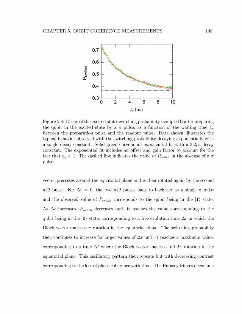
CHAPTER 5. QUBIT COHERENCE MEASUREMENTS 148
Figure 5.8: Decay of the excited state switching probability (sample B) after preparingthe qubit in the excited state by a � pulse, as a function of the waiting time twbetween the preparation pulse and the readout pulse. Data shown illustrates thetypical behavior observed with the switching probability decaying exponentially witha single decay constant. Solid green curve is an exponential �t with a 3.2�s decayconstant. The exponential �t includes an o¤set and gain factor to account for thefact that �d < 1. The dashed line indicates the value of Pswitch in the absense of a �pulse.
vector precesses around the equatorial plane and is then rotated again by the second
�=2 pulse. For �t = 0, the two �=2 pulses back to back act as a single � pulse
and the observed value of Pswitch corresponds to the qubit being in the j1i state.
As �t increases, Pswitch decreases until it reaches the value corresponding to the
qubit being in the j0i state, corresponding to a free evolution time �t in which the
Bloch vector makes a � rotation in the equatorial plane. The switching probability
then continues to increase for larger values of �t until it reaches a maximum value,
corresponding to a time �t where the Bloch vector makes a full 2� rotation in the
equatorial plane. This oscillatory pattern then repeats but with decreasing contrast
corresponding to the loss of phase coherence with time. The Ramsey fringes decay in a
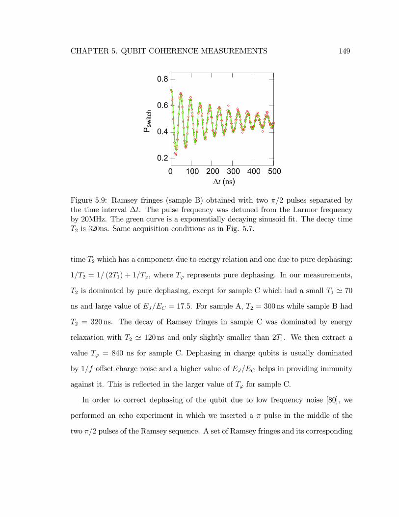
CHAPTER 5. QUBIT COHERENCE MEASUREMENTS 149
Figure 5.9: Ramsey fringes (sample B) obtained with two �=2 pulses separated bythe time interval �t. The pulse frequency was detuned from the Larmor frequencyby 20MHz. The green curve is a exponentially decaying sinusoid �t. The decay timeT2 is 320ns. Same acquisition conditions as in Fig. 5.7.
time T2 which has a component due to energy relation and one due to pure dephasing:
1=T2 = 1= (2T1) + 1=T', where T' represents pure dephasing. In our measurements,
T2 is dominated by pure dephasing, except for sample C which had a small T1 ' 70
ns and large value of EJ=EC = 17:5. For sample A, T2 = 300 ns while sample B had
T2 = 320 ns. The decay of Ramsey fringes in sample C was dominated by energy
relaxation with T2 ' 120 ns and only slightly smaller than 2T1. We then extract a
value T' = 840 ns for sample C. Dephasing in charge qubits is usually dominated
by 1=f o¤set charge noise and a higher value of EJ=EC helps in providing immunity
against it. This is re�ected in the larger value of T' for sample C.
In order to correct dephasing of the qubit due to low frequency noise [80], we
performed an echo experiment in which we inserted a � pulse in the middle of the
two �=2 pulses of the Ramsey sequence. A set of Ramsey fringes and its corresponding

CHAPTER 5. QUBIT COHERENCE MEASUREMENTS 150
echo decay are shown in Fig. 5.10 for sample B. For this sample, the decay constant
was increased to 400 � 500 ns using the echo technique. For sample A, the echo
technique did not increase the phase coherence time. We believe that for sample A,
which has a larger ratio of EJ=EC than sample B,and hence protected from 1=f o¤set
charge noise, the dominant source of dephasing is due to broadband noise emanating
from residual photons in our readout resonator [81], thus explaining the ine¢ cacy
of the echo sequence. It is possible that the 50 environment shunting the qubit
on the phase port side was not fully thermalized to the refrigerator temperature of
10mK. For sample B, where an improvement was observed with the echo sequence,
there are likely two contributing factors. First, the ratio EJ=EC is much smaller
and o¤set charge noise played a stronger role. The low frequency component of this
noise can be corrected using an echo sequence. Second, we added more cryogenic
attenuation in the transmission lines directly coupling to the phase port to reduce
the resonator temperature, thereby potentially reducing the number of excess photons
in the readout resonator and their associated dephasing.
5.5 Readout �delity
We now come to question of the measurement �delity of the JBA readout. In all the
data shown in earlier sections, we note that the change in switching probability of
the JBA when the qubit makes a transition from the ground to the excited state, is
about 40 � 60%. An ideal readout would have a 100% change. This was one of the
main problems plaguing the quantronium qubit with a readout based on the switching
of the large Josephson junction from the superconducting state to the �nite voltage
state [6]. The central motivation for the development of the JBA was to improve
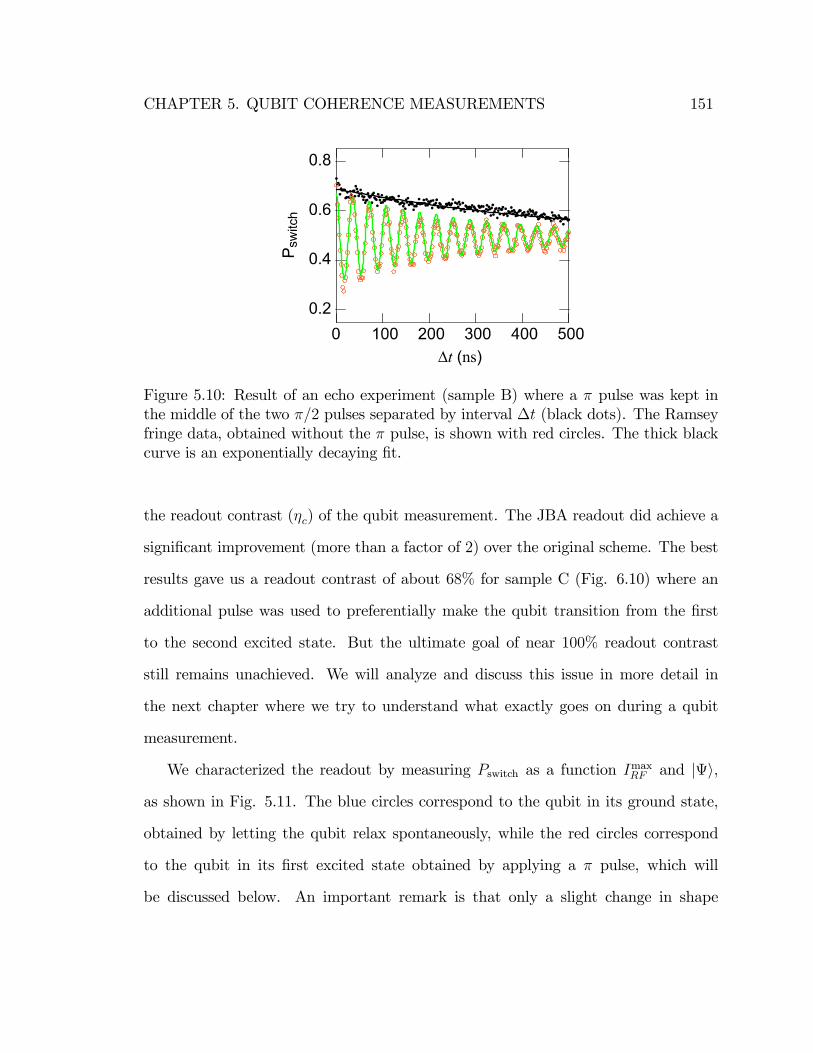
CHAPTER 5. QUBIT COHERENCE MEASUREMENTS 151
Figure 5.10: Result of an echo experiment (sample B) where a � pulse was kept inthe middle of the two �=2 pulses separated by interval �t (black dots). The Ramseyfringe data, obtained without the � pulse, is shown with red circles. The thick blackcurve is an exponentially decaying �t.
the readout contrast (�c) of the qubit measurement. The JBA readout did achieve a
signi�cant improvement (more than a factor of 2) over the original scheme. The best
results gave us a readout contrast of about 68% for sample C (Fig. 6.10) where an
additional pulse was used to preferentially make the qubit transition from the �rst
to the second excited state. But the ultimate goal of near 100% readout contrast
still remains unachieved. We will analyze and discuss this issue in more detail in
the next chapter where we try to understand what exactly goes on during a qubit
measurement.
We characterized the readout by measuring Pswitch as a function ImaxRF and ji,
as shown in Fig. 5.11. The blue circles correspond to the qubit in its ground state,
obtained by letting the qubit relax spontaneously, while the red circles correspond
to the qubit in its �rst excited state obtained by applying a � pulse, which will
be discussed below. An important remark is that only a slight change in shape
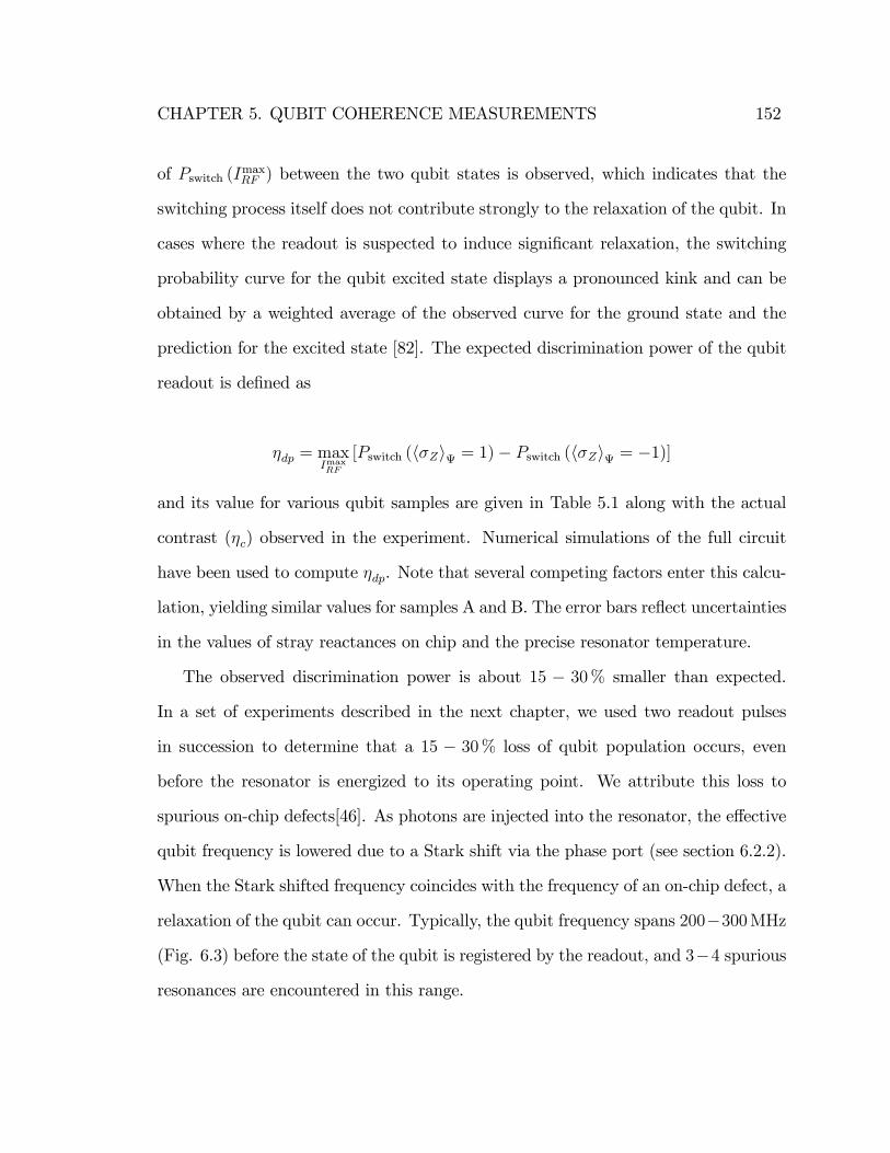
CHAPTER 5. QUBIT COHERENCE MEASUREMENTS 152
of Pswitch (ImaxRF ) between the two qubit states is observed, which indicates that the
switching process itself does not contribute strongly to the relaxation of the qubit. In
cases where the readout is suspected to induce signi�cant relaxation, the switching
probability curve for the qubit excited state displays a pronounced kink and can be
obtained by a weighted average of the observed curve for the ground state and the
prediction for the excited state [82]. The expected discrimination power of the qubit
readout is de�ned as
�dp = maxImaxRF
[Pswitch (h�Zi = 1)� Pswitch (h�Zi = �1)]
and its value for various qubit samples are given in Table 5.1 along with the actual
contrast (�c) observed in the experiment. Numerical simulations of the full circuit
have been used to compute �dp. Note that several competing factors enter this calcu-
lation, yielding similar values for samples A and B. The error bars re�ect uncertainties
in the values of stray reactances on chip and the precise resonator temperature.
The observed discrimination power is about 15 � 30% smaller than expected.
In a set of experiments described in the next chapter, we used two readout pulses
in succession to determine that a 15 � 30% loss of qubit population occurs, even
before the resonator is energized to its operating point. We attribute this loss to
spurious on-chip defects[46]. As photons are injected into the resonator, the e¤ective
qubit frequency is lowered due to a Stark shift via the phase port (see section 6.2.2).
When the Stark shifted frequency coincides with the frequency of an on-chip defect, a
relaxation of the qubit can occur. Typically, the qubit frequency spans 200�300MHz
(Fig. 6.3) before the state of the qubit is registered by the readout, and 3�4 spurious
resonances are encountered in this range.

CHAPTER 5. QUBIT COHERENCE MEASUREMENTS 153
Figure 5.11: Switching probability as a function of maximum drive current and qubitstate for sample B. The vertical dotted line represents value of drive current at whichmaximal discrimination power is observed. The width in current of the curves is inreasonable agreement with numerical simulations (data not shown). The solid lineconnects the observed data points in the j0i state and the dashed line is a copy of thesolid line horizontally shifted to overlap the j1i state data at low values of Pswitch.
We also note from Table 5.1 that the expected discrimination power for samples
A and B was only 0:70. To increase the expected discrimination power, we must
use samples with either a larger qubit EJ or a stronger phase coupling between the
qubit and readout resonator. We used the latter approach in sample C by replacing
the large Josephson junction in the quantronium with two Josephson junctions in
series. This provided us with an expected discrimination close to unity but the
measured discrimination power showed only marginal improvement. Note that a
stronger coupling between the qubit and the resonator also leads to a larger shift in
e¤ective qubit frequency as the resonator is energized, leading to a possibly larger
loss of qubit population. Even the smallest loss in qubit population before the actual
measurement will prevent you from achieving 100% readout �delity.
CHAPTER 5. QUBIT COHERENCE MEASUREMENTS 154
In conclusion, we have successfully implemented a non-linear dispersive readout of
the quantronium qubit using the Josephson Bifurcation Ampli�er. The readout speed
and discrimination power show a signi�cant improvement when compared with the
DC switching readout used in the original quantronium measurements [6]. Perhaps
even more important, in the present readout scheme, the total measurement time is
much smaller than T1, and it is possible to carry out experiments with multiple read-
out pulses to determine the information �ow during a qubit readout and to account
for any losses in qubit population. This important aspect can be used to determine
the degree to which the measurement is quantum non-demolishing. These ideas are
discussed in more detail in the next chapter.
Chapter 6
Qubit readout performance
In this chapter we will discuss the performance of the JBA as a qubit readout. We
saw in the previous chapter that it was theoretically possible to choose qubit and
JBA parameters to achieve a single shot readout. Experimentally we found that
the contrast was smaller than the predicted value. In this chapter, we would like to
analyze the possible causes of this reduced performance and provide a possible �x to
the problem. Speci�cally, we would like to separate the intrinsic sensitivity of the
JBA from other processes taking place during the readout operation which might
lead to reduced performance. We begin by discussing the quantum non-demolition
nature of the qubit readout with the JBA which allows successive measurements of
the qubit state to be carried out. We will then break down the readout process and
describe the evolution of the qubit state during the readout. The AC Stark shift of
the qubit Larmor frequency when the JBA is energized will then be described and we
will discuss its consequences on the readout process. Finally, we will discuss possible
methods by which the goal of a single-shot readout can be achieved.
155

CHAPTER 6. QUBIT READOUT PERFORMANCE 156
6.1 Quantum non-demolition readout using a JBA
Quantum non-demolition measurements are basically the ideal, textbook measure-
ments of a quantum system (see ref. [83] for a review). The measurement process
yields one of the eigenvalues of the measured observable and the quantum state imme-
diately after the measurement is the eigenstate corresponding that eigenvalue. Since
the eigenstate does not evolve under the free evolution of the system, one can then
repeatedly measure the eigenstate achieving the same result everytime. This is the
most important aspect of a QND measurement. QND measurements were originally
discussed in the context of gravitational wave detection using massive metal bars
[84]. They can also be useful in optical communication for tapping the signal from an
optical �bre without a¤ecting it. QND measurements can also be used for entangling
several quantum systems.
A measurement involves coupling a quantum system to a measuring system which
we call the "meter". The total Hamiltonian of the combined system can be written
as a sum of three terms
Htotal = HQ + HM + HI (6.1)
where HQ,HM ,HI are the Hamiltonians of the the quantum system, the meter and
the interaction between them respectively. If we call the measured observable of
the quantum system as AQ, then a QND measurement requires the following two
conditions
hHI ; AQ
i= 0 (6.2a)h
HQ; AQ
i= 0 (6.2b)
CHAPTER 6. QUBIT READOUT PERFORMANCE 157
The �rst condition ensures that there is no back-action of the meter on the measured
observable1 while the second condition ensures that the projected state does not evolve
after that measurement. In chapter 4, we derived the combined Hamiltonian of the
quantronium with the JBA (4.26) which we reproduce below for no gate excitation
(U (t) = 0)
Htotal = �EJ2�Z + �~!p�Zaya+ (6.3)
~!paya� ��1 +
�
4�Z
��a+ ay
�4 � f �a+ ay� I (t)The �rst term is the qubit Hamiltonian (HQ), the second term is the dominant2
interaction Hamiltonian (HI) while the rest of the terms constitute the Hamiltonian
of the driven, non-linear resonator - our meter (HM). The coe¢ cients � and � are
de�ned in equations 4.27b and 4.27c. If we choose �Z as our observable, then we
note that the QND conditions 6.2a and 6.2b are satis�ed. We should point out that
equation 6.3 was derived for the case of zero asymmetry (d = 0) in the quantronium
junctions (see 4.1.3) and only in this limit the QND conditions are fully satis�ed. For
�nite values of d, corrections to the QND fraction of order d2 exist [79].
With the QND conditions being satis�ed for the quantronium with a JBA readout,
we can make multiple measurements of the qubit state and determine the extent to
which they are QND. The fact that the qubits have a �nite lifetime for the excited
state is somewhat contradictory to the requirement that the qubit state should not
1A measurement always involves some backaction but the quantity being a¤ected could be dif-ferent than the one being observed. In this case, the backaction leads to dephasing of the qubit butdoes not cause any mixing of the qubit states.
2There is also a coupling term (/ �) between the qubit and the non-linear part of the resonator.We neglect that term in this analysis for simplicity as it does not a¤ect the QND nature of thereadout.
CHAPTER 6. QUBIT READOUT PERFORMANCE 158
evolve between measurements. Since any measurement requires a �nite amount of
time to complete, there is always a �nite probability for the qubit to decay to its
ground state leading to errors in the subsequent measurements. But we can always
factor this out if we know the lifetime of the qubit excited state. In the next section,
we will discuss the results of multiple measurements of the qubit state and explore in
more detail the evolution of the qubit state during measurement.
6.2 Information �ow during qubit measurement
6.2.1 Multiple pulse measurements
The qubit was prepared in its ground state and then multiple readout pulses were
used to measure the qubit. This was repeated thousands of times to construct the
switching probability for each pulse. We observed that with the qubit in the ground
state, the switching probability associated with each pulse was the same, indicating
that the qubit remained in the ground state after every measurement. The same
procedure when repeated with the qubit prepared in the excited state, led to some
interesting results. In Fig. 6.1 we show the result of multiple measurements of the
excited state of the qubit for di¤erent readout frequencies. Data is shown for sample
A with !01=2� = 18:989 GHz (see Table 5.1). The plasma frequency of the JBA
readout was !p=2� = 1:81 GHz.
The switching probability data has been normalized and converted into a prob-
ability Pj1i of the qubit being in the excited state, by using the result of the �rst
measurement assuming that the �rst pulse makes a perfect measurement of the qubit
state. The time axis indicates the time delay between the � pulse used to prepare
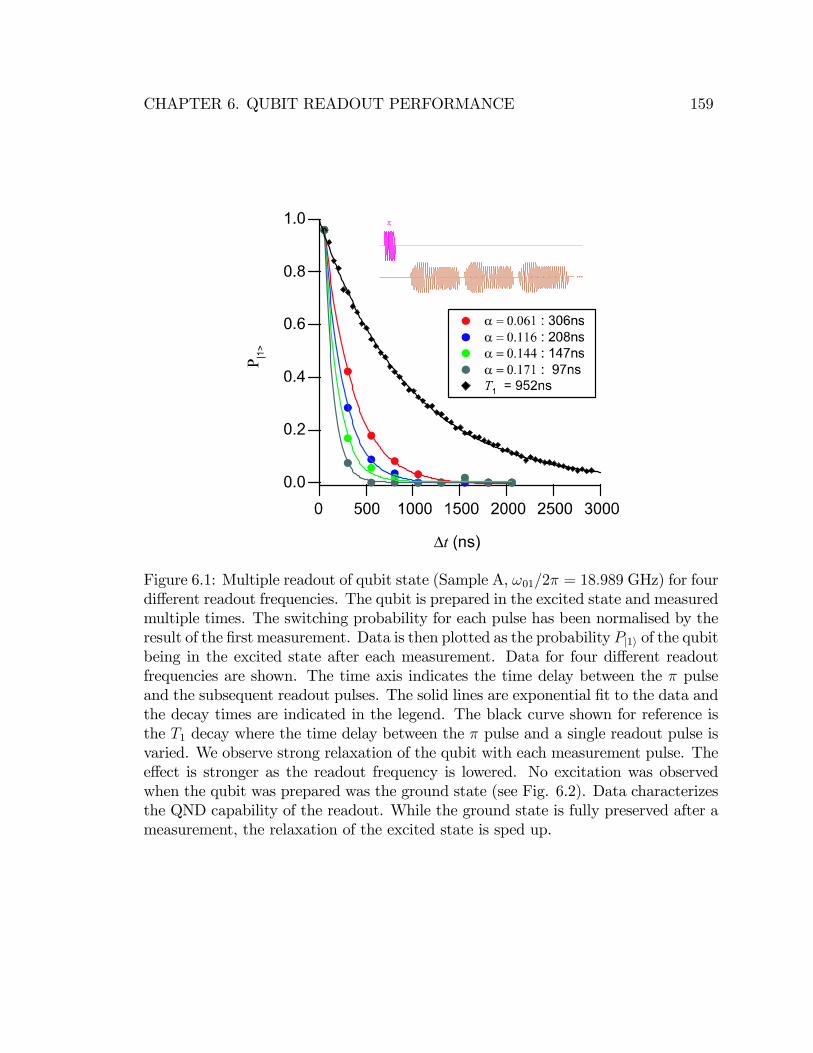
CHAPTER 6. QUBIT READOUT PERFORMANCE 159
Figure 6.1: Multiple readout of qubit state (Sample A, !01=2� = 18:989 GHz) for fourdi¤erent readout frequencies. The qubit is prepared in the excited state and measuredmultiple times. The switching probability for each pulse has been normalised by theresult of the �rst measurement. Data is then plotted as the probability Pj1i of the qubitbeing in the excited state after each measurement. Data for four di¤erent readoutfrequencies are shown. The time axis indicates the time delay between the � pulseand the subsequent readout pulses. The solid lines are exponential �t to the data andthe decay times are indicated in the legend. The black curve shown for reference isthe T1 decay where the time delay between the � pulse and a single readout pulse isvaried. We observe strong relaxation of the qubit with each measurement pulse. Thee¤ect is stronger as the readout frequency is lowered. No excitation was observedwhen the qubit was prepared was the ground state (see Fig. 6.2). Data characterizesthe QND capability of the readout. While the ground state is fully preserved after ameasurement, the relaxation of the excited state is sped up.
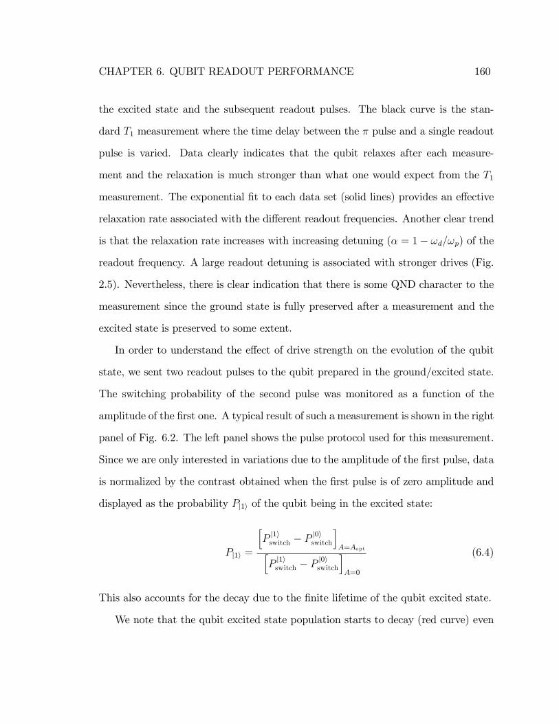
CHAPTER 6. QUBIT READOUT PERFORMANCE 160
the excited state and the subsequent readout pulses. The black curve is the stan-
dard T1 measurement where the time delay between the � pulse and a single readout
pulse is varied. Data clearly indicates that the qubit relaxes after each measure-
ment and the relaxation is much stronger than what one would expect from the T1
measurement. The exponential �t to each data set (solid lines) provides an e¤ective
relaxation rate associated with the di¤erent readout frequencies. Another clear trend
is that the relaxation rate increases with increasing detuning (� = 1� !d=!p) of the
readout frequency. A large readout detuning is associated with stronger drives (Fig.
2.5). Nevertheless, there is clear indication that there is some QND character to the
measurement since the ground state is fully preserved after a measurement and the
excited state is preserved to some extent.
In order to understand the e¤ect of drive strength on the evolution of the qubit
state, we sent two readout pulses to the qubit prepared in the ground/excited state.
The switching probability of the second pulse was monitored as a function of the
amplitude of the �rst one. A typical result of such a measurement is shown in the right
panel of Fig. 6.2. The left panel shows the pulse protocol used for this measurement.
Since we are only interested in variations due to the amplitude of the �rst pulse, data
is normalized by the contrast obtained when the �rst pulse is of zero amplitude and
displayed as the probability Pj1i of the qubit being in the excited state:
Pj1i =
hPj1iswitch � P
j0iswitch
iA=Aopth
Pj1iswitch � P
j0iswitch
iA=0
(6.4)
This also accounts for the decay due to the �nite lifetime of the qubit excited state.
We note that the qubit excited state population starts to decay (red curve) even
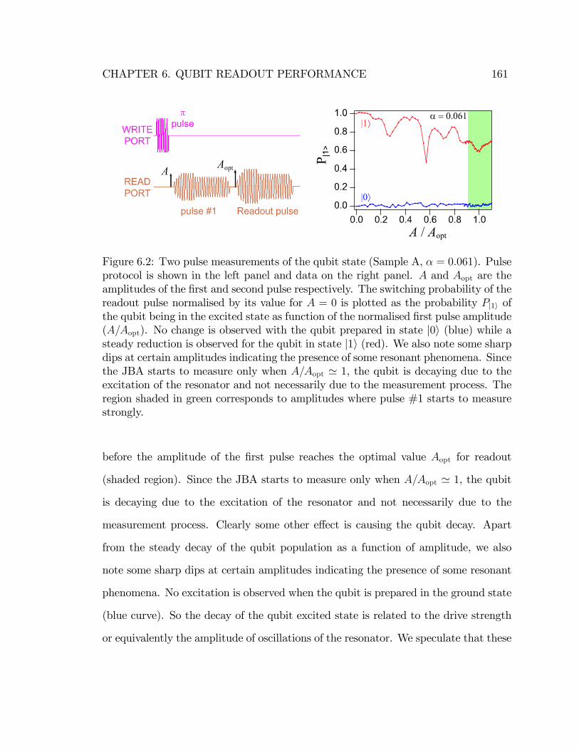
CHAPTER 6. QUBIT READOUT PERFORMANCE 161
Figure 6.2: Two pulse measurements of the qubit state (Sample A, � = 0:061). Pulseprotocol is shown in the left panel and data on the right panel. A and Aopt are theamplitudes of the �rst and second pulse respectively. The switching probability of thereadout pulse normalised by its value for A = 0 is plotted as the probability Pj1i ofthe qubit being in the excited state as function of the normalised �rst pulse amplitude(A=Aopt). No change is observed with the qubit prepared in state j0i (blue) while asteady reduction is observed for the qubit in state j1i (red). We also note some sharpdips at certain amplitudes indicating the presence of some resonant phenomena. Sincethe JBA starts to measure only when A=Aopt ' 1, the qubit is decaying due to theexcitation of the resonator and not necessarily due to the measurement process. Theregion shaded in green corresponds to amplitudes where pulse #1 starts to measurestrongly.
before the amplitude of the �rst pulse reaches the optimal value Aopt for readout
(shaded region). Since the JBA starts to measure only when A=Aopt ' 1, the qubit
is decaying due to the excitation of the resonator and not necessarily due to the
measurement process. Clearly some other e¤ect is causing the qubit decay. Apart
from the steady decay of the qubit population as a function of amplitude, we also
note some sharp dips at certain amplitudes indicating the presence of some resonant
phenomena. No excitation is observed when the qubit is prepared in the ground state
(blue curve). So the decay of the qubit excited state is related to the drive strength
or equivalently the amplitude of oscillations of the resonator. We speculate that these
CHAPTER 6. QUBIT READOUT PERFORMANCE 162
losses are due to resonances in the qubit environment arising from on-chip defects. As
the oscillation amplitude of the resonator increases, the e¤ective qubit frequency is
lowered due to a Stark shift [47] via the phase port. When the Stark shifted frequency
coincides with the frequency of an on-chip defect, a relaxation of the qubit can occur.
We characterize this frequency shift next.
6.2.2 AC Stark shift of qubit
The shifting of the qubit frequency due to the energizing of the oscillator can be
understood in two ways. From the discussion in section 4.1.3, we know the qubit
Hamiltonian and hence the Larmor frequency is a function of the two control pa-
rameters - Ng and � (4.6). When the resonator coupled to the qubit via the phase
port is energized, the phase � across the qubit oscillates, resulting in a modulation
of the qubit Larmor frequency. The frequency modulation which takes place at the
resonator drive frequency results in an average shift of the Larmor frequency. The
Larmor frequency is maximum at the phase bias point (� = 0) for the qubit and
decreases with increasing � and this results in the lowering of the Larmor frequency
in the presence of driving on the phase port. A similar e¤ect can be achieved if we
drive the gate port (Ng) with a frequency far detuned from the Larmor frequency to
prevent qubit excitation. But now, the direction of shift is towards higher frequen-
cies because the Larmor frequency is the smallest at the gate bias point (Ng = 0:5).
We can also understand the AC Stark shift via the phase port in another way by

CHAPTER 6. QUBIT READOUT PERFORMANCE 163
combining the �rst two terms in the Hamiltonian in 6.3 and writing it as
Htotal = ��EJ � 2�~!paya
� �Z2+ (6.5)
~!paya� ��1 +
�
4�Z
��a+ ay
�4 � f �a+ ay� I (t)The �rst term can now be seen as a spin 1=2 with a Larmor frequency which is
dependent on the number of photons (hayai) in the resonator [47]-the frequency shift
per photon being 2�~!p.
In order to calibrate these frequency shifts as a function of the readout amplitude,
we carried out the two pulse measurement described above with a small modi�cation.
With the qubit prepared in the ground state, we added a probe microwave signal on
the gate port overlapping in time with the �rst pulse which we now call the Stark
pulse (see Fig. 6.3). When the amplitude of the Stark pulse is large enough to
Stark shift the qubit (prepared in its ground state) into resonance with the probe
signal, we observe enhancement in Pswitch of the readout pulse #2 indicating resonant
excitation of the qubit. By repeating this measurement for di¤erent probe frequencies
(!probe < !01), we can map out the Stark shifted qubit frequency as a function of the
drive amplitude. A similar experiment can be carried out to calibrate the Stark shift
from the gate port with both the Stark and the probe pulse being applied to the gate
port. The result of such measurements on Sample B is shown in Fig. 6.3.
Panel (a) shows the pulse protocol used for this measurement. Panel (b) plots
Pswitch as a function of drive amplitude for three di¤erent probe frequencies. The
position of the peak corresponds to the amplitude at which the qubit is Stark shifted
into resonance with the probe frequency. Panel (c) maps out this dependence and
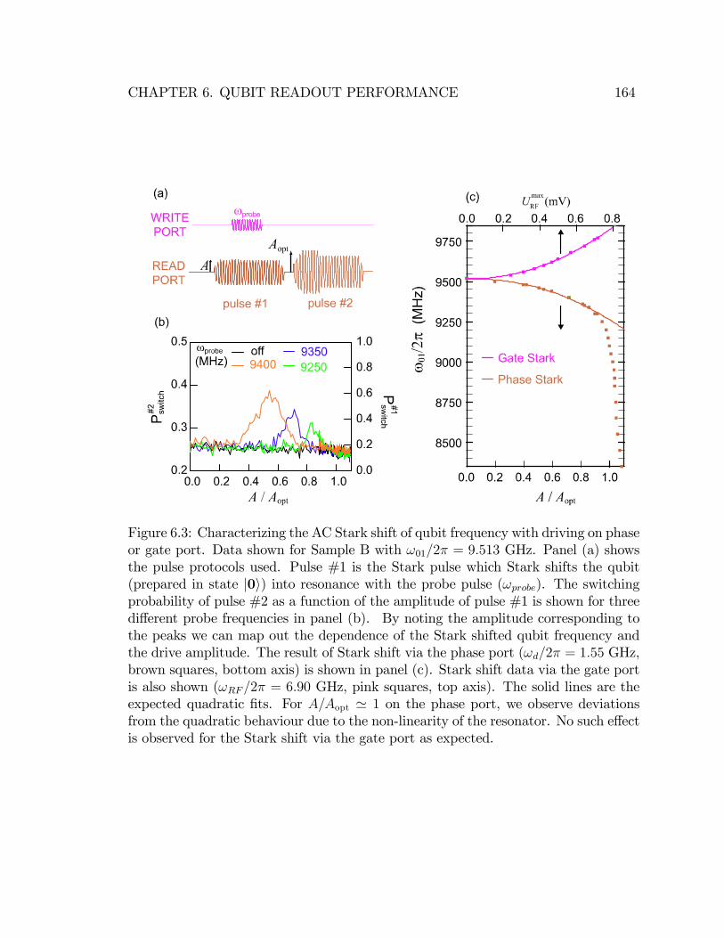
CHAPTER 6. QUBIT READOUT PERFORMANCE 164
Figure 6.3: Characterizing the AC Stark shift of qubit frequency with driving on phaseor gate port. Data shown for Sample B with !01=2� = 9:513 GHz. Panel (a) showsthe pulse protocols used. Pulse #1 is the Stark pulse which Stark shifts the qubit(prepared in state j0i) into resonance with the probe pulse (!probe). The switchingprobability of pulse #2 as a function of the amplitude of pulse #1 is shown for threedi¤erent probe frequencies in panel (b). By noting the amplitude corresponding tothe peaks we can map out the dependence of the Stark shifted qubit frequency andthe drive amplitude. The result of Stark shift via the phase port (!d=2� = 1:55 GHz,brown squares, bottom axis) is shown in panel (c). Stark shift data via the gate portis also shown (!RF=2� = 6:90 GHz, pink squares, top axis). The solid lines are theexpected quadratic �ts. For A=Aopt ' 1 on the phase port, we observe deviationsfrom the quadratic behaviour due to the non-linearity of the resonator. No such e¤ectis observed for the Stark shift via the gate port as expected.

CHAPTER 6. QUBIT READOUT PERFORMANCE 165
plots the Stark shifted frequency as a function of drive amplitude for both phase
and gate driving. The solid lines are quadratic �ts to the data which indicate that
the Stark shift is proportional to the drive power and hence photon number in the
resonator. For drive amplitudes close to Aopt, the non-linearity of the resonator starts
coming into play and the frequency starts to change much faster. This is because the
oscillation amplitude now grows non-linearly with the drive amplitude. Also, for
A=Aopt � 1, the JBA starts to switch into its high amplitude state resulting in much
larger Stark shifts. No such e¤ect is observed for AC Stark shift via the gate port as
expected, since the oscillation amplitude of Ng is directly proportional to the drive
amplitude UmaxRF .
6.2.3 Quantifying the losses during readout
In order to quantify the loss in qubit population during readout, we came up with
a model to illustrate the evolution of the qubit state during di¤erent parts of the
readout pulse. Note that this is a very simplistic model and might not account for all
scenarios. The model evolved from analyzing typical qubit behavior in experiments.
Nevertheless, it provides a simple way to separate the intrinsic discrimination power
of the readout from the losses due to qubit decay. This model is illustrated in Fig.
6.4.
The readout pulse is separated into four parts - ARM, PROJECT, RECORD and
DISARM. The ARM phase is when the JBA is energized up to the optimal level for
readout. The PROJECT phase is when the qubit state is projected and the JBA
ends up in its low or high amplitude state. In the RECORD phase, the result of
measurement is latched and recorded and �nally in the DISARM phase the readout
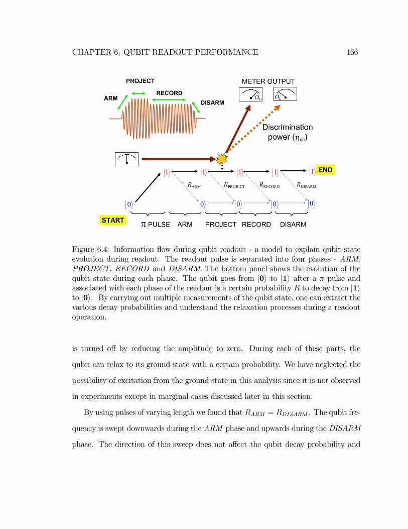
CHAPTER 6. QUBIT READOUT PERFORMANCE 166
Figure 6.4: Information �ow during qubit readout - a model to explain qubit stateevolution during readout. The readout pulse is separated into four phases - ARM,PROJECT, RECORD and DISARM. The bottom panel shows the evolution of thequbit state during each phase. The qubit goes from j0i to j1i after a � pulse andassociated with each phase of the readout is a certain probability R to decay from j1ito j0i. By carrying out multiple measurements of the qubit state, one can extract thevarious decay probabilities and understand the relaxation processes during a readoutoperation.
is turned o¤ by reducing the amplitude to zero. During each of these parts, the
qubit can relax to its ground state with a certain probability. We have neglected the
possibility of excitation from the ground state in this analysis since it is not observed
in experiments except in marginal cases discussed later in this section.
By using pulses of varying length we found that RARM = RDISARM . The qubit fre-
quency is swept downwards during the ARM phase and upwards during the DISARM
phase. The direction of this sweep does not a¤ect the qubit decay probability and

CHAPTER 6. QUBIT READOUT PERFORMANCE 167
hence RARM = RDISARM . Also, we found that the decay during the PROJECT phase
is usually smaller than the ARM phase and hence we can set3 that RPROJECT = 0.
Given these constraints we can analyze the data shown in Fig. 6.5 which shows data
for di¤erent readout frequencies with the �rst pulse amplitude close to Aopt. The
data for smaller amplitudes for the �rst pulse is similar to Fig. 6.2.
Also shown for reference are the switching probability curves for the ground and
excited state obtained from the �rst measurement pulse. For a single readout, only
the ARM and PROJECT phase is encountered, and we can write
�f = (1�RARM) (1�RPROJECT ) �dp (6.6)
where �f is the readout �delity (obtained from the observed contrast after accounting
for T1 losses) and �dp is the actual discrimination power of the readout (see 4.3.5).
From the data in Fig. 6.5, if we take the value of the qubit excited state population
(PAj1i) at an amplitude just before the S-curves start (indicated by dashed line A), we
get the losses associated with the ARM and DISARM phase of the readout
(1�RARM) (1�RDISARM) = PAj1i (6.7)
Solving for RARM = RDISARM (� 1), we get
RARM = 1�qPAj1i (6.8)
3This assumption need not always be true. The decay during the PROJECT phase can accountedas a modi�ed T1 e¤ect. Note that the T1 of the qubit while it is being driven can be di¤erent than theundriven T1 as shown later. It is also possible to combine the PROJECT and ARM phase together.We usually observed that the dominant relaxation before the actual measurement was due to theARM phase.
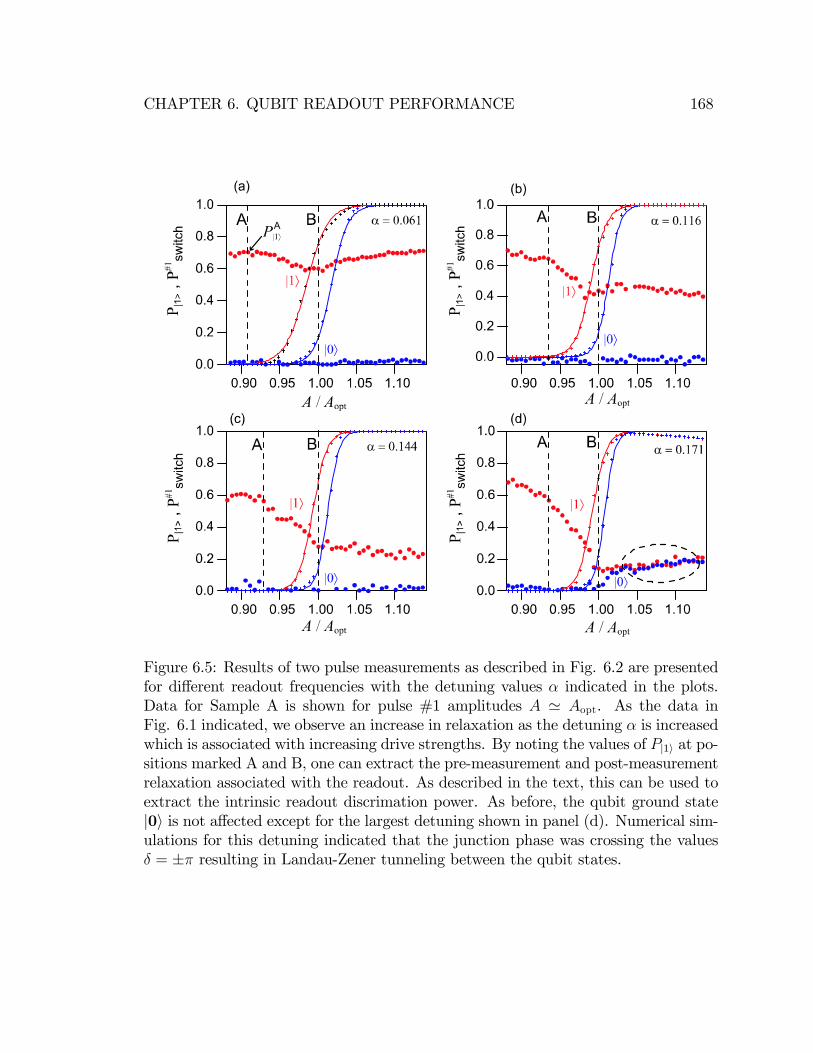
CHAPTER 6. QUBIT READOUT PERFORMANCE 168
Figure 6.5: Results of two pulse measurements as described in Fig. 6.2 are presentedfor di¤erent readout frequencies with the detuning values � indicated in the plots.Data for Sample A is shown for pulse #1 amplitudes A ' Aopt. As the data inFig. 6.1 indicated, we observe an increase in relaxation as the detuning � is increasedwhich is associated with increasing drive strengths. By noting the values of Pj1i at po-sitions marked A and B, one can extract the pre-measurement and post-measurementrelaxation associated with the readout. As described in the text, this can be used toextract the intrinsic readout discrimation power. As before, the qubit ground statej0i is not a¤ected except for the largest detuning shown in panel (d). Numerical sim-ulations for this detuning indicated that the junction phase was crossing the values� = �� resulting in Landau-Zener tunneling between the qubit states.
CHAPTER 6. QUBIT READOUT PERFORMANCE 169
Setting RPROJECT = 0, we can solve for �dp
�dp =�fqPAj1i
(6.9)
The value of Pj1i at an amplitude equal to the optimal readout amplitude (indicated
by dashed line B) tells us about the fraction of qubit excited state population which
survives after a full readout operation. We call this the QND fraction FQND given by
FQND = (1�RARM) (1�RDISARM) (1�RRECORD) = PBj1i (6.10)
where we have set RPROJECT = 0. Solving for RRECORD, we get
RRECORD = 1� PBj1i=PAj1i (6.11)
Processing the data in Fig. 6.5 using the technique described we can compute RARM
and RRECORD for the di¤erent readout frequencies. The result is summarized as
a function of readout detuning � in Fig. 6.6. The pre-measurement relaxation
(RARM) has a weak dependence on the detuning but the post-measurement relaxation
(RRECORD) has a very strong dependence. This implies that the observed contrast
doesn�t vary much with detuning4 as can been seen from the S-curves in Fig. 6.5. The
QND fraction which depends on RRECORD must decreases strongly with detuning as
we saw in Fig. 6.1.
We note that the data in Fig. 6.5d show some excitation of the qubit state for
4This is because the discrimination power �dp also does not vary much with detuning.
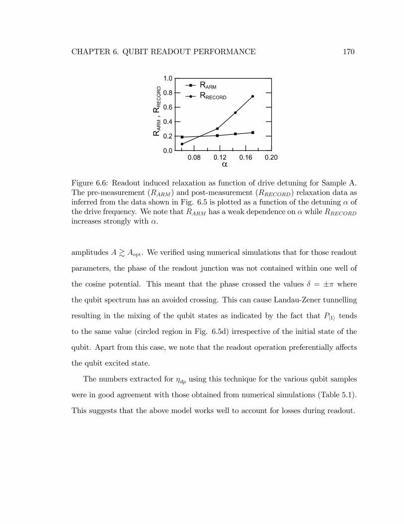
CHAPTER 6. QUBIT READOUT PERFORMANCE 170
Figure 6.6: Readout induced relaxation as function of drive detuning for Sample A.The pre-measurement (RARM) and post-measurement (RRECORD) relaxation data asinferred from the data shown in Fig. 6.5 is plotted as a function of the detuning � ofthe drive frequency. We note that RARM has a weak dependence on � while RRECORDincreases strongly with �.
amplitudes A & Aopt. We veri�ed using numerical simulations that for those readout
parameters, the phase of the readout junction was not contained within one well of
the cosine potential. This meant that the phase crossed the values � = �� where
the qubit spectrum has an avoided crossing. This can cause Landau-Zener tunnelling
resulting in the mixing of the qubit states as indicated by the fact that Pj1i tends
to the same value (circled region in Fig. 6.5d) irrespective of the initial state of the
qubit. Apart from this case, we note that the readout operation preferentially a¤ects
the qubit excited state.
The numbers extracted for �dp using this technique for the various qubit samples
were in good agreement with those obtained from numerical simulations (Table 5.1).
This suggests that the above model works well to account for losses during readout.

CHAPTER 6. QUBIT READOUT PERFORMANCE 171
6.3 Characterizing the qubit environment
It is clear from the data shown in the previous sections that the losses in the envi-
ronment seen by the qubit have an important role to play in the performance of the
qubit and its readout. The T1 measurements discussed in chapter 5 are not com-
patible with the values that would be expected from the designed electromagnetic
environment [40]. The decoherence in the qubit is set by the properties of an un-
controlled environment coupled to the qubit. It has been conjectured that the losses
are due to a collection of two level �uctuators (TLF) which could be present in the
substrate, in the oxide layer covering the metallic electrodes or in the oxide barrier
of the junction [85]. Such TLFs have been routinely observed as avoided crossings
in the spectroscopy of phase qubits which use large area Josephson junctions [46].
They have also been observed in CPB based qubits which typically use small area
Josephson junctions, though their occurrence is rarer [40, 86]. This collection of TLFs
usually result in an e¤ective, frequency dependent, lossy bath, but coherent coupling
between the qubit and the TLF has also been observed.
Fig. 6.7 shows spectroscopy data for sample C. Panel (a) shows the data obtained
in the �rst cooldown. The qubit frequency was varied by applying a magnetic �eld.
Each row is a plot of Pswitch (mean subtracted) plotted as a color v.s. qubit transition
frequency. The red regions correspond to the frequency where the excitation frequency
matches the qubit transition frequency. The dashed line is the expected dependence
calculated using the EJ and EC values for this sample (Table 5.1). One can clearly
observe a strong avoided crossing (� 0:2 GHz splitting) around 19:5 GHz along with
some weaker cutouts in the spectrum at a few other locations. There is also a cutout
in the spectrum at the sweet spot (�=�0 = 0) which explains the extremely low
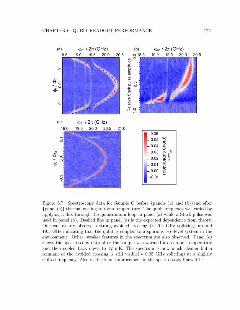
CHAPTER 6. QUBIT READOUT PERFORMANCE 172
Figure 6.7: Spectroscopy data for Sample C before {panels (a) and (b)}and after{panel (c)} thermal cycling to room temperature. The qubit frequency was varied byapplying a �ux through the quantronium loop in panel (a) while a Stark pulse wasused in panel (b). Dashed line in panel (a) is the expected dependence from theory.One can clearly observe a strong avoided crossing (� 0:2 GHz splitting) around19:5 GHz indicating that the qubit is coupled to a spurious two-level system in theenvironment. Other, weaker features in the spectrum are also observed. Panel (c)shows the spectroscopy data after the sample was warmed up to room temperatureand then cooled back down to 12 mK. The spectrum is now much cleaner but aremnant of the avoided crossing is still visible(� 0:05 GHz splitting) at a slightlyshifted frequency. Also visible is an improvement in the spectroscopy linewidth.
CHAPTER 6. QUBIT READOUT PERFORMANCE 173
T1(< 10 ns) which was observed during the �rst cooldown. Panel (b) shows the same
data taken using a Stark pulse to shift the qubit frequency. Sample C had two readout
junctions in series for enhanced coupling to the split CPB, resulting in much larger
Stark shifts (� 1:6 GHz) as compared to sample B (� 0:2 GHz, 6.3). This is for Stark
pulse amplitudes less than those required for the JBA to switch. We can explain the
factor of 8 di¤erence observed in the maximum Stark shift between Sample B and
Sample C as follows. The two readout junctions double the phase excursion across the
split CPB resulting in 4 times the Start shift (quadratic dependence on amplitude).
The remaining factor of 2 is due to the Larmor frequency of Sample C being roughly
twice that of Sample B.
Panel (c) shows the spectroscopy performed on sample C after the sample was
warmed up to room temperature and cooled back down to 12 mK. The data is now
much cleaner with fewer cutouts. There is still a remnant of the avoided crossing
at 19:5 GHz which is now slightly shifted in frequency and weaker (� 0:05 GHz
splitting). Also, the cutout at the sweet spot is no longer present, resulting in an
improved T1 � 70 ns. This kind of behavior with temperature cycling is often seen
in solid state systems. The temperature cycling can lead to the rearrangement of the
microscopic defects leading to a change in the spectrum of the environment.
We also used T1 measurements as a way to characterize the environment as it is
a probe for the available decay modes at the qubit transition frequency. A common
feature we observed in all samples is the dependence of T1 on gate voltage U . Ideally,
the qubit properties should be the same as long as Ngmod 1 = 0:5, the sweet spot in
charge. But in practice, we always found that certain values of U where better than
others in terms of stability and T1 values. This variation of T1 with gate voltage for
CHAPTER 6. QUBIT READOUT PERFORMANCE 174
Sample B is shown in Fig. 6.8a. We note that variations in T1 of about a factor of two
is observed. The data point with the largest positive gate voltage had a parity jump
where one extra electron gets onto the island. Often, the gate voltage at which best
results are obtained changes with time. This dependence on gate voltage suggests that
the loss mechanism must involve some charged TLFs. Note that the qubit transition
frequency is kept the same as we are always biased at the sweet spot. In another
set of T1 measurements shown Fig. 6.8b, we varied the qubit transition frequency
by threading a �ux through the loop of the quantronium while keeping Ng = 0:5.
Again, we note variations as large as a factor of two while the expected variation
from theory is much smaller. We observe similar behavior when the frequency is
varied by changing gate charge. These kind of variations in T1 have been seen in
other superconducting qubit measurements [40].
Qubit properties like T1 can di¤er when they are driven by a strong �eld [40],
like during a readout operation. We carried out T1 measurements on Sample B in
the presence of strong driving on the phase and gate port. As discussed in 6.2.2,
driving the qubit on the gate or phase port leads to an AC Stark shift of the qubit
frequency. This is another way of characterizing the frequency dependence of the
qubit environment, though the driving can lead to additional e¤ects. Results of such
measurements are shown in Fig. 6.9. The measurement protocol is similar to the one
described in 5.4, but now we include a Stark pulse on either the gate or the phase
port during the time delay between the � pulse and the readout pulse.
We again see strong variations in T1 for di¤erent Stark shifted qubit frequencies.
The dashed line indicates the undriven Larmor frequency of the qubit. We also note
an overall reduction in T1 as the driving strength is increased, though the e¤ect is
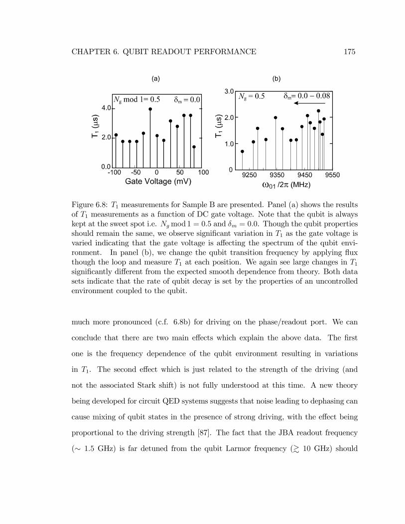
CHAPTER 6. QUBIT READOUT PERFORMANCE 175
Figure 6.8: T1 measurements for Sample B are presented. Panel (a) shows the resultsof T1 measurements as a function of DC gate voltage. Note that the qubit is alwayskept at the sweet spot i.e. Ngmod 1 = 0:5 and �m = 0:0. Though the qubit propertiesshould remain the same, we observe signi�cant variation in T1 as the gate voltage isvaried indicating that the gate voltage is a¤ecting the spectrum of the qubit envi-ronment. In panel (b), we change the qubit transition frequency by applying �uxthough the loop and measure T1 at each position. We again see large changes in T1signi�cantly di¤erent from the expected smooth dependence from theory. Both datasets indicate that the rate of qubit decay is set by the properties of an uncontrolledenvironment coupled to the qubit.
much more pronounced (c.f. 6.8b) for driving on the phase/readout port. We can
conclude that there are two main e¤ects which explain the above data. The �rst
one is the frequency dependence of the qubit environment resulting in variations
in T1. The second e¤ect which is just related to the strength of the driving (and
not the associated Stark shift) is not fully understood at this time. A new theory
being developed for circuit QED systems suggests that noise leading to dephasing can
cause mixing of qubit states in the presence of strong driving, with the e¤ect being
proportional to the driving strength [87]. The fact that the JBA readout frequency
(� 1:5 GHz) is far detuned from the qubit Larmor frequency (& 10 GHz) should
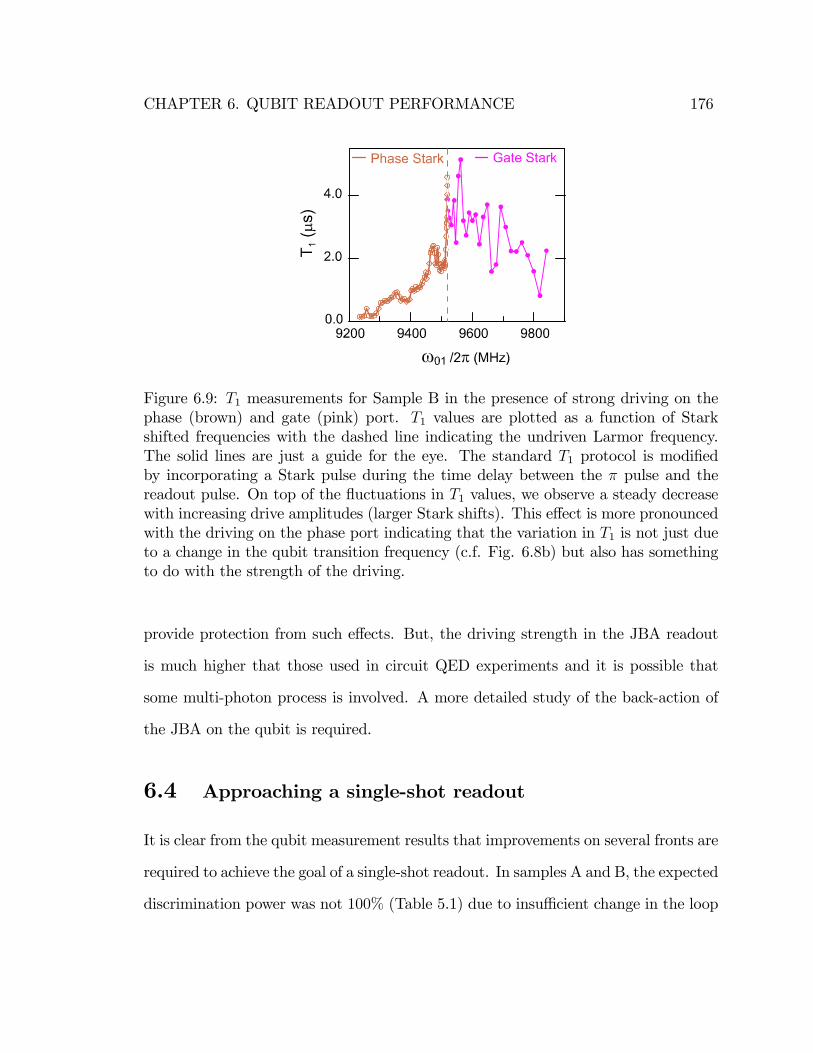
CHAPTER 6. QUBIT READOUT PERFORMANCE 176
Figure 6.9: T1 measurements for Sample B in the presence of strong driving on thephase (brown) and gate (pink) port. T1 values are plotted as a function of Starkshifted frequencies with the dashed line indicating the undriven Larmor frequency.The solid lines are just a guide for the eye. The standard T1 protocol is modi�edby incorporating a Stark pulse during the time delay between the � pulse and thereadout pulse. On top of the �uctuations in T1 values, we observe a steady decreasewith increasing drive amplitudes (larger Stark shifts). This e¤ect is more pronouncedwith the driving on the phase port indicating that the variation in T1 is not just dueto a change in the qubit transition frequency (c.f. Fig. 6.8b) but also has somethingto do with the strength of the driving.
provide protection from such e¤ects. But, the driving strength in the JBA readout
is much higher that those used in circuit QED experiments and it is possible that
some multi-photon process is involved. A more detailed study of the back-action of
the JBA on the qubit is required.
6.4 Approaching a single-shot readout
It is clear from the qubit measurement results that improvements on several fronts are
required to achieve the goal of a single-shot readout. In samples A and B, the expected
discrimination power was not 100% (Table 5.1) due to insu¢ cient change in the loop
CHAPTER 6. QUBIT READOUT PERFORMANCE 177
currents between the ground and the excited state. In order to increase this signal, we
developed the double junction JBA (DJBA) where the readout junction was replaced
by two readout junctions in series. This roughly doubled the coupling between the
readout junction and the qubit which was con�rmed by numerical simulations (section
4.4). Samples C was made with the DJBA readout and the measured S-curves are
shown in Fig. 6.10a.
The measured contrast is about 40% while the calculated discrimination power
is 95%. Using the two pulse experiment described above, we found that the qubit
relaxation during the ARM+PROJECT phase was much stronger (roughly 3 times)
in this sample as compared to samples A and B, resulting in a reduced contrast. We
believe that this is due to the much larger Stark shifts observed in the DJBA samples
due to the enhanced coupling with the qubit. The larger excursion in frequency
space results in a higher probability of encountering environmental resonances and
hence relaxation. This sample also had a much smaller T1 and as is evident from
Fig. 6.7, had several environmental resonances near the qubit Larmor frequency.
Nevertheless, we were able to improve the contrast further in sample C by using the
following technique. Due to the large EJ=EC (= 17:5) ratio, we were able to access
the second excited state j2i. The transition frequency between the �rst and second
excited state (!12 = 18:275 GHz) is now smaller than !01 = 20:344 GHz. It turns
out that for these qubit parameters, the change in the e¤ective critical current of the
split CPB is almost double in state j2i as compared to state j1i. The measurement
protocol now involves applying a � pulse at !12 before the readout operation. If the
qubit is initially in state j0i, it would remain in that state while if the qubit is in state
j1i, it would be transformed to j2i. In general, a qubit state �1j0i+ �2j1i would be
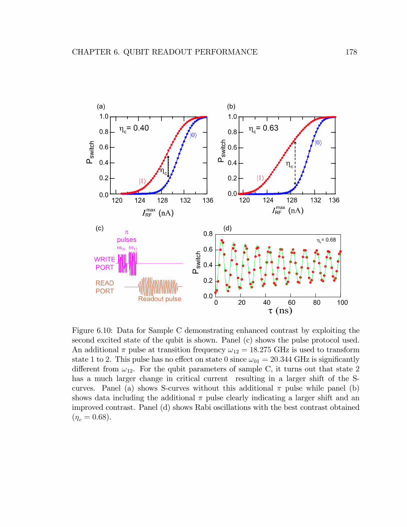
CHAPTER 6. QUBIT READOUT PERFORMANCE 178
Figure 6.10: Data for Sample C demonstrating enhanced contrast by exploiting thesecond excited state of the qubit is shown. Panel (c) shows the pulse protocol used.An additional � pulse at transition frequency !12 = 18:275 GHz is used to transformstate 1 to 2. This pulse has no e¤ect on state 0 since !01 = 20:344 GHz is signi�cantlydi¤erent from !12. For the qubit parameters of sample C, it turns out that state 2has a much larger change in critical current resulting in a larger shift of the S-curves. Panel (a) shows S-curves without this additional � pulse while panel (b)shows data including the additional � pulse clearly indicating a larger shift and animproved contrast. Panel (d) shows Rabi oscillations with the best contrast obtained(�c = 0:68).
CHAPTER 6. QUBIT READOUT PERFORMANCE 179
transformed to �1j0i+ �2j2i.
The S-curves measured using this new technique are shown in Fig. 6.10·c. We
note an improved contrast �c = 0:63. The excited state S-curve (red) is now shifted
more because it now corresponds to the qubit being in state j2i which has a smaller
e¤ective critical current. There are still losses associated with the energizing of the
oscillator but overall we observe an improvement in the contrast. The excited state
S-curve is now a weighted average of the S-curve in state j2i, j1i and j0i depending
on the probability of decay from state j2i to j1i and from state j1i to j0i. There are
two e¤ects which result in the improved contrast. As explained above, the �rst one is
the larger change in e¤ective critical current in state j2i, though the e¤ective critical
current change for state j1i was already large enough to obtain �dp = 0:95. We believe
that a more important e¤ect is the fact that the qubit in state j2i is now sensitive to a
di¤erent range of frequencies. Due to the selection rules for the qubit transitions, the
most probable way for the qubit to relax is from j2i to j1i and then from j1i to j0i.
For the qubit to decay from j2i to j1i, the relevant frequency is !12 = 18:275 GHz.
As the oscillator is energized this frequency gets Stark shifted to lower frequencies.
It is possible that this frequency range has less environmental resonances resulting in
a reduced probability of relaxation during readout. The best contrast obtained using
this technique was about 68% as illustrated by the Rabi oscillation data shown in
Fig. 6.10d.
In conclusion, getting the qubit readout contrast within a few % of unity is an
important problem that needs to be solved for quantum computing applications. This
will allow interesting experiments like measuring the entanglement of multiple qubits
and testing Bell�s inequality [88] with good signal to noise. A single-shot readout
CHAPTER 6. QUBIT READOUT PERFORMANCE 180
will also enable more stringent tests of the theory of quantum measurements and
understanding the evolution of the qubit during a measurement operation [89].
The superconducting qubit community is yet to achieve a readout with near 100%
e¢ ciency but steady progress is being made. Phase qubits with about 90% readout
contrast are in the front of the race [90]. Flux qubits have demonstrated 87% contrast
using a non-linear resonator readout like the JBA [91]. They were able to change the
qubit frequency rapidly by applying �ux pulses just before the readout operation.
This way they were able to minimize the relaxation of the qubit during readout,
resulting in a better contrast. Circuit QED systems with charge qubits coupled to
superconducting cavities have achieved 100% visibility with weak measurements [86]
but the readout contrast is often limited to about 30% [92]. This has been improved
recently to about 70% [93]. They are mostly limited due to the noise temperature of
their following ampli�er but also observe mixing of qubit states when using a large
number of photons for measurement. Experiments using a CBA, the distributed ele-
ment version of the JBA, to measure the quantronium qubit have achieved a readout
contrast of 60% [43] though very recent CBA measurements using low Q (� 100),
coplanar stripline resonators indicate a readout contrast of about 85% [94].
All these di¤erent systems ultimately su¤er from some kind of qubit relaxation
during the readout process. The uncontrolled losses in the qubit environment are
partly responsible for this relaxation and hence further research in improving the
quality of the materials used in fabrication is required. Nevertheless, there is still
scope for improvement in readout design which might enable one to achieve 100%
readout contrast. A two stage readout process where a weak, yet projective mea-
surement is followed by a stronger ampli�cation stage to improve the signal to noise
CHAPTER 6. QUBIT READOUT PERFORMANCE 181
ratio seems to be a promising way for solving the problem. An example would be to
measure a qubit coupled to a linear resonator with a few photons and following it up
with a non-linear system like the JBA or a parametric ampli�er for further gain.
Chapter 7
Quantum escape and parametric ampli�cation:
Theory
In this chapter, we will address the problem of transitions between the metastable
states of the JBA in the quantum regime. In the classical regime, the transitions
are governed by an activation process with thermal noise activating the system over
an e¤ective barrier (see section 2.3.2 and ref. [27]). Now, we want to consider the
case as T ! 0 [49, 50]. What mechanism governs the transitions as T ! 0 ? Is there
tunneling between the metastable states or does a di¤erent mechanism exists? More
importantly, what sets the classical to quantum crossover temperature? Borrowing
ideas from the theory of macroscopic quantum tunnelling (MQT) in current biased
Josephson junctions [95, 48], we can make an educated guess that the crossover tem-
perature must be related to the plasma frequency of the oscillator. We will try to
answer these questions in the next few sections.
We will begin by discussing Input-Output theory (see [96] and reference therein)
and how we can use it to compute escape rates out of metastable states. We will treat
182
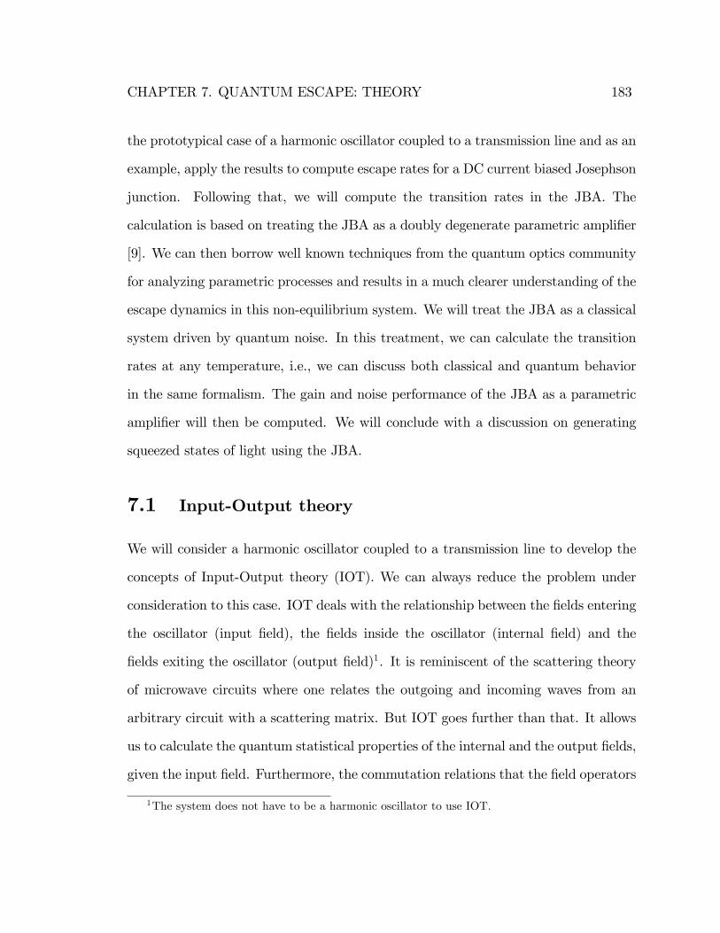
CHAPTER 7. QUANTUM ESCAPE: THEORY 183
the prototypical case of a harmonic oscillator coupled to a transmission line and as an
example, apply the results to compute escape rates for a DC current biased Josephson
junction. Following that, we will compute the transition rates in the JBA. The
calculation is based on treating the JBA as a doubly degenerate parametric ampli�er
[9]. We can then borrow well known techniques from the quantum optics community
for analyzing parametric processes and results in a much clearer understanding of the
escape dynamics in this non-equilibrium system. We will treat the JBA as a classical
system driven by quantum noise. In this treatment, we can calculate the transition
rates at any temperature, i.e., we can discuss both classical and quantum behavior
in the same formalism. The gain and noise performance of the JBA as a parametric
ampli�er will then be computed. We will conclude with a discussion on generating
squeezed states of light using the JBA.
7.1 Input-Output theory
We will consider a harmonic oscillator coupled to a transmission line to develop the
concepts of Input-Output theory (IOT). We can always reduce the problem under
consideration to this case. IOT deals with the relationship between the �elds entering
the oscillator (input �eld), the �elds inside the oscillator (internal �eld) and the
�elds exiting the oscillator (output �eld)1. It is reminiscent of the scattering theory
of microwave circuits where one relates the outgoing and incoming waves from an
arbitrary circuit with a scattering matrix. But IOT goes further than that. It allows
us to calculate the quantum statistical properties of the internal and the output �elds,
given the input �eld. Furthermore, the commutation relations that the �eld operators
1The system does not have to be a harmonic oscillator to use IOT.
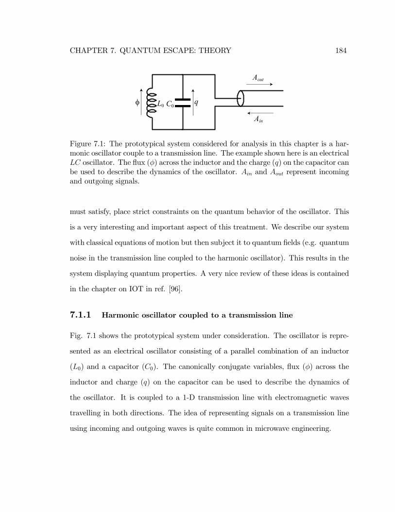
CHAPTER 7. QUANTUM ESCAPE: THEORY 184
Figure 7.1: The prototypical system considered for analysis in this chapter is a har-monic oscillator couple to a transmission line. The example shown here is an electricalLC oscillator. The �ux (�) across the inductor and the charge (q) on the capacitor canbe used to describe the dynamics of the oscillator. Ain and Aout represent incomingand outgoing signals.
must satisfy, place strict constraints on the quantum behavior of the oscillator. This
is a very interesting and important aspect of this treatment. We describe our system
with classical equations of motion but then subject it to quantum �elds (e.g. quantum
noise in the transmission line coupled to the harmonic oscillator). This results in the
system displaying quantum properties. A very nice review of these ideas is contained
in the chapter on IOT in ref. [96].
7.1.1 Harmonic oscillator coupled to a transmission line
Fig. 7.1 shows the prototypical system under consideration. The oscillator is repre-
sented as an electrical oscillator consisting of a parallel combination of an inductor
(L0) and a capacitor (C0). The canonically conjugate variables, �ux (�) across the
inductor and charge (q) on the capacitor can be used to describe the dynamics of
the oscillator. It is coupled to a 1-D transmission line with electromagnetic waves
travelling in both directions. The idea of representing signals on a transmission line
using incoming and outgoing waves is quite common in microwave engineering.
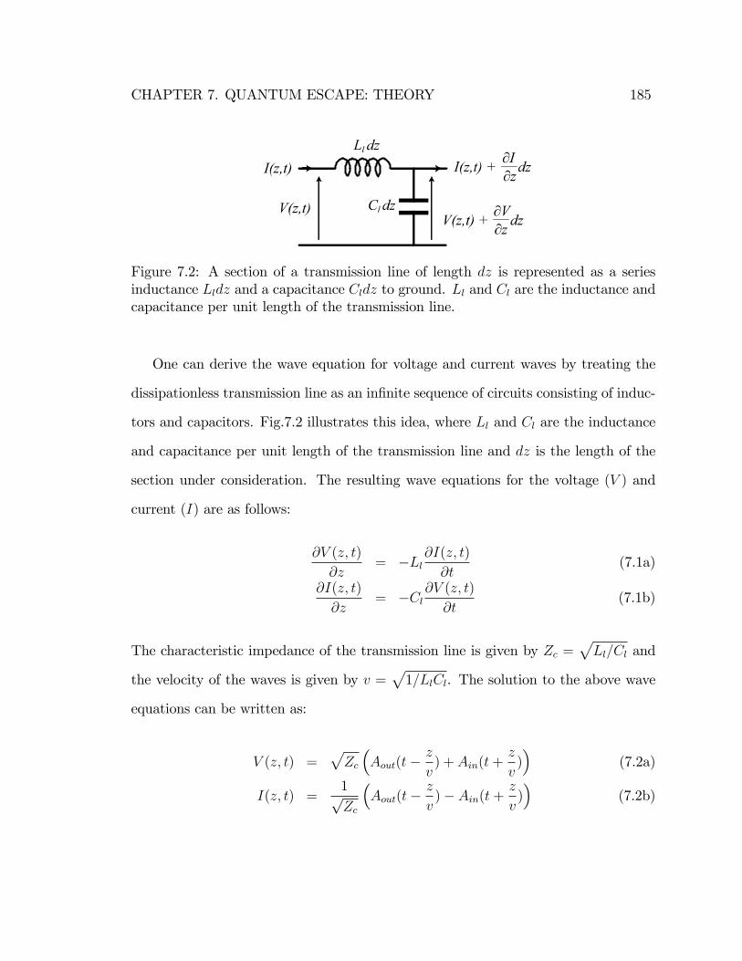
CHAPTER 7. QUANTUM ESCAPE: THEORY 185
Figure 7.2: A section of a transmission line of length dz is represented as a seriesinductance Lldz and a capacitance Cldz to ground. Ll and Cl are the inductance andcapacitance per unit length of the transmission line.
One can derive the wave equation for voltage and current waves by treating the
dissipationless transmission line as an in�nite sequence of circuits consisting of induc-
tors and capacitors. Fig.7.2 illustrates this idea, where Ll and Cl are the inductance
and capacitance per unit length of the transmission line and dz is the length of the
section under consideration. The resulting wave equations for the voltage (V ) and
current (I) are as follows:
@V (z; t)
@z= �Ll
@I(z; t)
@t(7.1a)
@I(z; t)
@z= �Cl
@V (z; t)
@t(7.1b)
The characteristic impedance of the transmission line is given by Zc =pLl=Cl and
the velocity of the waves is given by v =p1=LlCl. The solution to the above wave
equations can be written as:
V (z; t) =pZc
�Aout(t�
z
v) + Ain(t+
z
v)�
(7.2a)
I(z; t) =1pZc
�Aout(t�
z
v)� Ain(t+
z
v)�
(7.2b)
CHAPTER 7. QUANTUM ESCAPE: THEORY 186
Figure 7.3: The left panel shows a circuit driven by a voltage source Vs with sourceimpedance R. The right panel shows the same circuit now connected to a transmissionline with incoming (Ain) and outgoing (Aout) waves. The two cases depicted representthe same situation if we make the identi�cation Zc = R and Vs = 2
pRAin (t).
The voltage and current along the line can be represented as a linear superposition of
waves travelling in opposite directions. This gives now a concrete meaning to what
these waves represent. They could represent a signal launched on the transmission
line in order to drive the oscillator or they could represent the thermal/quantum
�uctuations in the transmission line. Note that the wave amplitudes Aout and Ain
have dimensions of square root of power. The total power crossing a point in the
transmission line is given by�jAinj2 � jAoutj2
�=2.
Fig. 7.3 gives an example of an arbitrary circuit driven by a voltage source Vs(t)
with internal resistance R. The right panel shows the same circuit connected to a
transmission line of characteristic impedance Zc = R with incoming and outgoing
waves.
The two cases depicted are equivalent if we make the identi�cation Zc = R and
Vs(t) = 2pRAin(t). If we set z = 0 (the location of the circuit) in equations 7.2a and
7.2b, the outgoing wave computes to:
Aout(t) =V (t)pZc� Ain(t) (7.3)

CHAPTER 7. QUANTUM ESCAPE: THEORY 187
These relations are derived by imposing the appropriate boundary conditions on the
solutions given by equations 7.2a and 7.2b. We can now compute the response of the
system given the input �eld. Equation 7.3 is the essence of IOT. It relates the input
�eld Ain, the internal �eld V (t), and the output �eld Aout. In the above example,
the voltage source Vs should not only represent the intended drive signal, but also
the Nyquist noise of the resistance R, in order to completely describe the problem.
In the examples that follow, we will separate any intentional drive signal (classical)
from the noise so that Ain only represents the noise, which we will describe quantum
mechanically from now on.
We introduce quantum mechanics into the picture by quantizing the �elds on the
transmission line and representing them in terms of creation (ayin [!]) and annihilation
(ain [!]) operators of the quantum modes of the transmission line:
Ain(t) =1
2�
Z 1
0
d!
r~!2
�ain[!] exp (�i!t) + ayin[!] exp (i!t)
�!(7.4)
The �eld operators ain[!] and ayin[!] satisfy the standard commutation relations for
1-D scalar �elds given below, where we have used the conventions described in [19, 20]
but we restrict ! to only have positive values:
hain[!]; a
yin [!
0]i= 2��(! � !0)
[ain[!]; ain [!0]] =
hayin[!]; a
yin [!
0]i= 0
hnain[!]; a
yin[!
0]oi = Saa (!) 2��(! � !0) (7.5)
Saa (!) = coth�~!2kBT
�
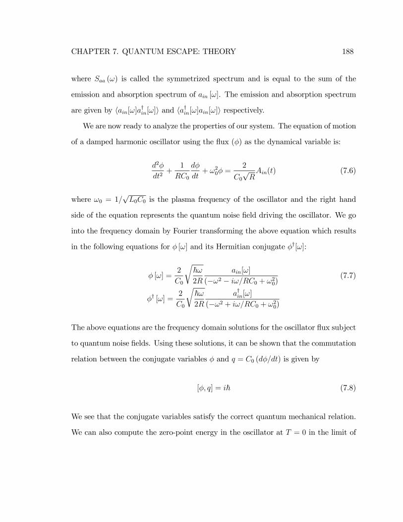
CHAPTER 7. QUANTUM ESCAPE: THEORY 188
where Saa (!) is called the symmetrized spectrum and is equal to the sum of the
emission and absorption spectrum of ain [!]. The emission and absorption spectrum
are given by hain[!]ayin[!]i and hayin[!]ain[!]i respectively.
We are now ready to analyze the properties of our system. The equation of motion
of a damped harmonic oscillator using the �ux (�) as the dynamical variable is:
d2�
dt2+
1
RC0
d�
dt+ !20� =
2
C0pRAin(t) (7.6)
where !0 = 1=pL0C0 is the plasma frequency of the oscillator and the right hand
side of the equation represents the quantum noise �eld driving the oscillator. We go
into the frequency domain by Fourier transforming the above equation which results
in the following equations for � [!] and its Hermitian conjugate �y[!]:
� [!] =2
C0
r~!2R
ain[!]
(�!2 � i!=RC0 + !20)(7.7)
�y [!] =2
C0
r~!2R
ayin[!]
(�!2 + i!=RC0 + !20)
The above equations are the frequency domain solutions for the oscillator �ux subject
to quantum noise �elds. Using these solutions, it can be shown that the commutation
relation between the conjugate variables � and q = C0 (d�=dt) is given by
[�; q] = i~ (7.8)
We see that the conjugate variables satisfy the correct quantum mechanical relation.
We can also compute the zero-point energy in the oscillator at T = 0 in the limit of
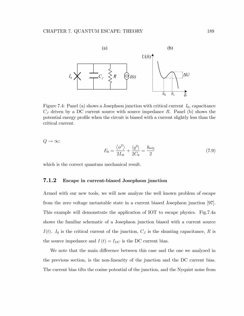
CHAPTER 7. QUANTUM ESCAPE: THEORY 189
Figure 7.4: Panel (a) shows a Josephson junction with critical current I0, capacitanceCJ driven by a DC current source with source impedance R. Panel (b) shows thepotential energy pro�le when the circuit is biased with a current slightly less than thecritical current.
Q!1:
E0 =
�2�
2L0+hq2i2C0
=~!02
(7.9)
which is the correct quantum mechanical result.
7.1.2 Escape in current-biased Josephson junction
Armed with our new tools, we will now analyze the well known problem of escape
from the zero voltage metastable state in a current biased Josephson junction [97].
This example will demonstrate the application of IOT to escape physics. Fig.7.4a
shows the familiar schematic of a Josephson junction biased with a current source
I(t). I0 is the critical current of the junction, CJ is the shunting capacitance, R is
the source impedance and I (t) = IDC is the DC current bias.
We note that the main di¤erence between this case and the one we analyzed in
the previous section, is the non-linearity of the junction and the DC current bias.
The current bias tilts the cosine potential of the junction, and the Nyquist noise from
CHAPTER 7. QUANTUM ESCAPE: THEORY 190
the resistor causes the junction to switch from the zero voltage state. We include the
e¤ect of the classical DC current drive in the classical equation of the motion for the
system and replace the resistor by a transmission line of characteristic impedance R.
Representing the quantum noise as an incoming �eld as before, we get the following
equation:
'0CJd2�
dt2+'0R
d�
dt+ I0 sin (�)� IDC =
2pRAin(t) (7.10)
where � = �='0 is the superconducting phase di¤erence across the junction and '0 is
the reduced �ux quantum. In the absence of noise, the junction will develop a phase
� = �0 = sin�1 (IDC=I0). This is the metastable state of the junction. The �uctuations
in � induced by the incoming noise cause transitions out of this metastable state. The
escape happens when � �uctuates from the equilibrium point �0 and reaches �s. This
point �s, where U (�) has a maximum as shown Fig. 7.4b, corresponds to a saddle
point in the phase space (�; _�) and hence is known as the saddle point. In order to
compute the �uctuations induced in � due to the noise, we expand the above equation
around the equilibrium point � = �0, i.e., we write � = �0 + x, where x is our new
dynamical variable. Substituting this in the above equation and retaining only terms
up to �rst order in x, we get:
d2x
dt2+
1
RCJ
dx
dt+ ~!
2
px =2!2p
I0pRAin(t) (7.11)
where !p =pI0= ('0CJ) is the bare plasma frequency of the junction, while ~!p =
!p(1� (I=IDC)2)1=4 is the reduced plasma frequency. This is the step where we have
reduced the problem to an e¤ective harmonic oscillator driven by quantum noise,
as can be seen by comparing equation (7.11) with equation (7.6) and noting that

CHAPTER 7. QUANTUM ESCAPE: THEORY 191
Figure 7.5: The tilted washboard potential of a Josephson junction biased with aDC current IDC . I0, is shown here in the cubic approximation (red). The poten-tial representing the harmonic approximation is shown in green. �0 and �s are theequilibrium and the saddle points respectively. Also illustrated is the overestimationof the barrier height (�U� v.s. �U) in the harmonic approximation. The correctionfactor � can be found by using a value �x� at which the harmonic approximationgives the same barrier height as in the cubic case, and computes to � = 1=3.
x = �='0. The expression for the full potential for the DC biased junction is given
by:
U(�) = �'0I0 [cos (�) + � (IDC=I0)] (7.12)
In the limit when IDC=I0 ' 1, the tilted potential can be well approximated for
� ' �0 by a cubic potential. Fig. 7.5 shows the cubic potential (red) and the harmonic
approximation (green).
An important quantity for computing the escape probability is the distance from
the equilibrium point (�0) to the saddle point (�s). This is given by:
�x = �s � �0 = 2p2p1� IDC=I0 (7.13)
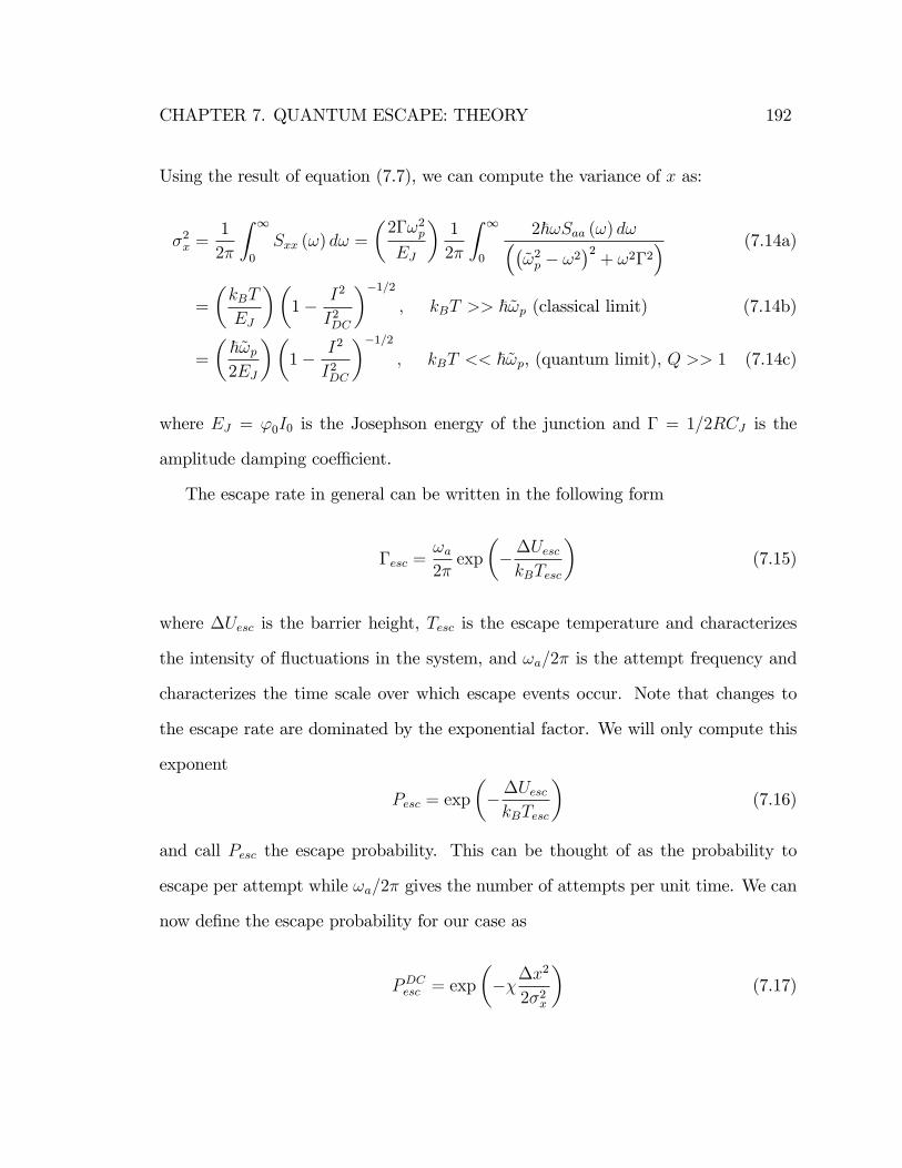
CHAPTER 7. QUANTUM ESCAPE: THEORY 192
Using the result of equation (7.7), we can compute the variance of x as:
�2x =1
2�
Z 1
0
Sxx (!) d! =
�2�!2pEJ
�1
2�
Z 1
0
2~!Saa (!) d!��~!2p � !2
�2+ !2�2
� (7.14a)
=
�kBT
EJ
��1� I2
I2DC
��1=2; kBT >> ~~!p (classical limit) (7.14b)
=
�~~!p2EJ
��1� I2
I2DC
��1=2; kBT << ~~!p, (quantum limit), Q >> 1 (7.14c)
where EJ = '0I0 is the Josephson energy of the junction and � = 1=2RCJ is the
amplitude damping coe¢ cient.
The escape rate in general can be written in the following form
�esc =!a2�exp
���UesckBTesc
�(7.15)
where �Uesc is the barrier height, Tesc is the escape temperature and characterizes
the intensity of �uctuations in the system, and !a=2� is the attempt frequency and
characterizes the time scale over which escape events occur. Note that changes to
the escape rate are dominated by the exponential factor. We will only compute this
exponent
Pesc = exp
���UesckBTesc
�(7.16)
and call Pesc the escape probability. This can be thought of as the probability to
escape per attempt while !a=2� gives the number of attempts per unit time. We can
now de�ne the escape probability for our case as
PDCesc = exp
����x
2
2�2x
�(7.17)

CHAPTER 7. QUANTUM ESCAPE: THEORY 193
which is the probability that x will �uctuate by �x given the variance �2x of its
distribution. Note how �x2 plays the role of �Uesc and �2x plays the role of Tesc. The
factor � in the exponent is a scaling constant which accounts for the overestimation of
the barrier height in the harmonic approximation for the potential. This is illustrated
in Fig. 7.5. Instead of using �x, we can use the value �x� for which the harmonic
approximation gives the same barrier height as the cubic potential. We compute the
value of � to be
� =1
3: (7.18)
Note that this is a general result for the harmonic approximation of the cubic poten-
tial. We will use this value of � when we compute the escape from the metastable
states of the JBA in the next section. Computing PDCesc using equation (7.17), we get
in the classical limit (kBT >> ~~!p)
PDCesc = exp
�4p2
3
EJkBT
�1� IDC
I0
�3=2!. (7.19)
The actual expression for the escape rate for the DC current biased Josephson junction
in the classical limit, is given by [97]
�DCesc =!p2�
�1� I2=I2DC
��1=2exp
�4p2
3
EJkBT
�1� IDC
I0
�3=2!. (7.20)
Comparing the above two equations, we can see that the exponents are identical. It is
important to note that in the harmonic approximation, we are analyzing the system
only for small �uctuations around the metastable minimum, while an escape event is
essentially a large �uctuation. Even though the average �uctuations are small, there
CHAPTER 7. QUANTUM ESCAPE: THEORY 194
is always a small probability for the system to make a large �uctuation leading to an
escape event. The use of the harmonic approximation is justi�ed because it does not
signi�cantly a¤ect the spectrum of the �uctuations as the system is predominantly
found near the minimum of the potential. The procedure is valid provided we work
with small escape probabilities.
In the quantum regime kBT << ~~!p, the escape out of the metastable state of
the DC current biased junction takes place via quantum tunneling. This process is
called Macroscopic Quantum Tunnelling (MQT) since it involves the tunneling of a
macroscopic quantity - the phase of the Josephson junction. In this regime, the escape
rate [95, 48] is given (in the high Q limit) by
�DC�MQTesc = ap
!p2�
�1� I2=I2DC
��1=2exp
�4p2
3
EJ~~!p=7:2
�1� IDC
I0
�3=2!(7.21)
where ap is a prefactor of order unity to account for �nite damping. We note that the
escape rate is now a constant independent of temperature with the e¤ective escape
temperature given by ~~!p=7:2kB. We can extend the method outlined in this section
to compute this result also. Note that the expression for �2x in the quantum limit
(7.14c) becomes independent of T and related to ~!p. But now these �uctuations in x
are arising from "virtual" zero point �uctuations and hence cannot activate over the
barrier. For tunneling through the barrier, we could use a di¤erent e¤ective �x in
the harmonic approximation to reproduce the result of equation 7.21.
We now have a method for computing exponents in the escape rates. In the next
section, we will apply this technique to the case of an RF driven Josephson oscillator.
We will be particularly interested in the quantum limit as T ! 0, and we will compare

CHAPTER 7. QUANTUM ESCAPE: THEORY 195
the results with the MQT case.
7.2 Escape dynamics in the JBA
We will begin by describing the JBA as a parametric ampli�er. We then proceed to
describe the system in the harmonic approximation so that we can use the techniques
developed in the previous section to compute escape rates.
7.2.1 Parametric ampli�er description of the JBA
We start with the classical equation of motion describing the driven, non-linear
Josephson oscillator. The initial part of this section reproduces some of the calcula-
tions done in section 2.2 to keep this chapter self-contained. We will use a slightly
di¤erent terminology as compared to chapter 2 to simplify calculations. We reproduce
equation 2.1 below, the starting point of our calculations:
CS'0d2�(t)
dt2+'0R
d�(t)
dt+ I0 sin(�(t)) = I(t) (7.22)
where CS is the total capacitance shunting the junction2, R is the impedance of the
transmission line to which the oscillator is coupled, I0 is the critical current of the
junction, � is the superconducting phase across the junction, '0 is the reduced �ux
quantum and I(t) is now the RF drive current. Rewriting the above equation for a
harmonic drive at frequency !d, and retaining only the �rst non-linear term in the
2We have ignored the junction capacitance CJ since CJ << CS .
CHAPTER 7. QUANTUM ESCAPE: THEORY 196
expansion of the sine term, we get:
d2�(t)
dt2+ 2�
d�(t)
dt+ !2p
��(t)� �(t)
3
6
�� !2p
IRFI0cos(!dt) =
2
CS'0pRAin(t) (7.23)
where !p = (I0=CS'0)1=2 is the plasma frequency of the oscillator (for small oscilla-
tions), � = 1=(2RCS) is the damping rate of the oscillation amplitude, and Ain is the
quantum noise felt by the oscillator written in �eld representation. As explained in
the previous section, we have separated the classical harmonic drive (IRF cos (!dt))
from the input �eld (Ain) which only represents the quantum noise. In order to com-
pute the steady state classical solution, we set Ain to zero and use the technique of
harmonic balance, i.e., we assume a steady state harmonic solution at frequency !d
of the form3:
�c(t) = �ck cos(!dt) + �c? sin(!dt) (7.24)
where �ck and �c? are the in-phase and quadrature-phase components of the classical
solution. We substitute this solution into the di¤erential equation and equate terms
at frequency !d. After eliminating terms at frequencies higher than !d, we get two
algebraic equations for �ck and �c? :
fdQ�ck + f
2d �c? + �c?
�2c? + �
2ck
8� 1!
= 0 (7.25a)
fdQ�c? � f 2d �ck � �ck
�2c? + �
2ck
8� 1!� iRF = 0
3We use the quadrature amplitude representation as described in 2.2.2 instead of the complexamplitudes of 2.2.1.
CHAPTER 7. QUANTUM ESCAPE: THEORY 197
where Q = RCS!p is the quality factor of the oscillator, fd = !d=!p is the dimension-
less drive frequency and iRF = IRF=I0 is the dimensionless drive current. The above
equations have three solutions in general. In the bistable regime, there are three
real valued solutions. The solution with the smallest (small amplitude state) and the
largest (large amplitude state) value of �2ck + �2c? represent the two metastable solu-
tions, while the third solution is the saddle point separating the two metastable states.
Fig.7.6 shows the solutions for some typical parameters, where �maxc =q�2k + �
2?. The
di¤erent curves correspond to di¤erent drive current amplitudes. We note that for
small values of drive current, there is only one solution, while above a certain drive
amplitude, three solutions are possible for certain drive frequencies.
Now we incorporate the e¤ect of noise and do a perturbation expansion (harmonic
approximation) around the classical solution, i.e., we look for solutions of the type:
�(t) = �c(t) + �q(t) (7.26)
where �c(t) is the steady state classical solution in the absence of noise, while �q(t)
is the quantum part of the solution in the presence of thermal/quantum noise. By
substituting the above solution into di¤erential equation(2.2), and retaining terms
only up to �rst order in �q(t), we get the di¤erential equation describing the dynamics
of �q(t) in the harmonic approximation:
d2�q(t)
dt2+ 2�
d�q(t)
dt+ !20(j�maxc j2 ; t)�q(t) =
2
CJ'0pRAin(t) (7.27)
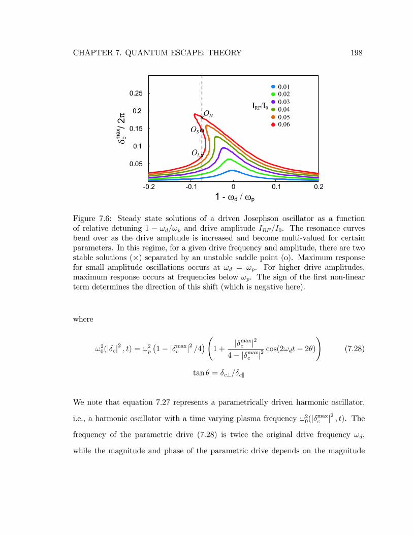
CHAPTER 7. QUANTUM ESCAPE: THEORY 198
Figure 7.6: Steady state solutions of a driven Josephson oscillator as a functionof relative detuning 1 � !d=!p and drive amplitude IRF=I0. The resonance curvesbend over as the drive ampltude is increased and become multi-valued for certainparameters. In this regime, for a given drive frequency and amplitude, there are twostable solutions (�) separated by an unstable saddle point (o). Maximum responsefor small amplitude oscillations occurs at !d = !p. For higher drive amplitudes,maximum response occurs at frequencies below !p. The sign of the �rst non-linearterm determines the direction of this shift (which is negative here).
where
!20(j�cj2 ; t) = !2p
�1� j�maxc j2 =4
� 1 +
j�maxc j2
4� j�maxc j2cos(2!dt� 2�)
!(7.28)
tan � = �c?=�ck
We note that equation 7.27 represents a parametrically driven harmonic oscillator,
i.e., a harmonic oscillator with a time varying plasma frequency !20(j�maxc j2 ; t). The
frequency of the parametric drive (7.28) is twice the original drive frequency !d,
while the magnitude and phase of the parametric drive depends on the magnitude
CHAPTER 7. QUANTUM ESCAPE: THEORY 199
and phase of the classical solution �c. This demonstrates that the system behaves
like a parametric ampli�er when biased near the bifurcation point, resulting in the
ampli�cation of quantum noise (Ain) which is feeding the oscillator. It is this am-
pli�cation of quantum noise we are interested in studying. In the presence of this
ampli�ed quantum noise, the steady-state solutions become metastable and the sys-
tem can make transitions from one steady state to another. By solving the above
equation, we can compute the �uctuations felt by the system and hence compute the
transition rates between the metastable states. In particular, we are interested in
the transition from the low amplitude state to the high amplitude state, the quantity
we usually measure in experiments. Also, when implemented as a qubit readout, the
JBA is biased near this transition and the width of this transition sets the ultimate
sensitivity of the JBA readout. Note that the above equation for the parametrically
driven oscillator does not display bistability due to the fact that we have only retained
the terms linear in �q(t).
7.2.2 Solutions in the frequency domain
The solutions to the di¤erential equation (7.27) are easily found by going to the
frequency domain. We de�ne the Fourier transform of �q(t) as �q[!] where the two
are related as given below:
�q (t) =1
2�
Z 1
0
��q [!] exp(�i!t) + �yq [!] exp(i!t)
�d!

CHAPTER 7. QUANTUM ESCAPE: THEORY 200
Note again that ! � 0. Taking the Fourier transform of equation(7.27), we get
�!2p (1� ")� !2 � i2�!
��q[!]�
!2p"
2exp(�2i�)�yq[2!d � !] (7.29)
=4�pR
'0
r~!2ain[!]
where " = �2c4; and
p~!=2ain[!] is the Fourier representation of Ain[t]. We have
ignored terms at frequencies which are a multiple of !d. Note how the above equa-
tion couples the creation and annihilation operator for �q, a characteristic feature
of parametrically driven systems. After making the rotating wave approximation
(!p + ! � 2!p, !=!p � 1) for the coe¢ cient of �q[!] in equation(7.29), and a change
of variable �q[!] =p~!=�EJx[!], we get after simplifying
�!p � !�
� !p"2�
� i�x[!]� !p"
4�exp(�2i�)xy[2!d � !] = ain[!] (7.30)
We now make the following transformations into dimensionless variables
!p � !�
� !p"2�
=!p � !d�
� ! � !d�
� !p"2�
= � f � 2� (7.31)
where
=!p � !d�
(7.32)
f =! � !d�
� =!p"
4�
Using the above transformation we can now write 7.30 as
CHAPTER 7. QUANTUM ESCAPE: THEORY 201
Figure 7.7: Gain functions jA (f)j2 and jB (f)j2 are plotted for �=�+B = 0:0; 0:85; 0:95where �+B is the value of � at the upper bifurcation point.. The functions jA (f)j
2 andjB (f)j2 represent the emission and absorption spectrum of xq at T = 0. The greencurve for �=�+B = 0:0 is the result for a harmonic oscilaltor subject to quantum noiseonly which has a �nite emission spectrum. As the system is driven to the bifurcationpoint, the absorption spectrum starts to grow due to parametric ampli�cation ofquantum noise. In a sense, the spectrum starts to look classical with equal values foremission and absorption.
(� 2�� f � i)x[�f ]� � exp(�2i�)xy[�f ] = ain[f ] (7.33)
where the dimensionless frequency f refers to an o¤set from the drive frequency !d
and can have negative values, i.e., �f $ !d � �f . The above equation along with
its Hermitian conjugate forms a set of four coupled algebraic equations. The solution
can be written as follows
x[�f ] = A (�f) ain [�f ] +B (�f) ayin [�f ] (7.34)
CHAPTER 7. QUANTUM ESCAPE: THEORY 202
where the functions A (f) and B (f) are given by
A(f) = � � 2�+ f + i�2 + (i+ f)2 � (� 2�)2
(7.35a)
B(f) = � � exp (2i�)
�2 + (i+ f)2 � (� 2�)2(7.35b)
The function A (f) links the annihilation operators of x with the annihilation op-
erators of ain, while B (f) links the annihilation operators of x with the creation
operators of ain. This connection between creation and annihilation operators is a
characteristic feature of any ampli�cation process. Fig.7.7 shows a plot of the func-
tions jA (f)j2 and jB (f)j2 which represent the emission and absorption spectrum of
xq for T = 0. The di¤erent curves correspond to di¤erent drive strengths approach-
ing the upper bifurcation point. Note how the peak in both functions shifts towards
the drive frequency and grows in magnitude as the bifurcation point is approached.
This indicates an increase in ampli�cation as one approaches the bifurcation point.
The green curve for �=�+B = 0:0 represents the harmonic oscillator with no parametric
driving and hence only the emission spectrum is �nite, re�ecting the spectrum of
quantum noise at T = 0. In section 7.3, we will discuss the operation of the JBA as
a parametric ampli�er and we will see how the functions A (f) and B (f) determine
the gain and noise performance of the ampli�er.
7.2.3 Quadrature variables
The escape dynamics for this problem can be described best in the quadrature variable
space. We will separate x (t) into its two quadrature components as we did for the

CHAPTER 7. QUANTUM ESCAPE: THEORY 203
Figure 7.8: The schematic illustrates the noise dynamics in the quadrature variablespace. Xjj and X? are the original axes used to describe the classical solutions with(0; 0) being the low amplitude state and (Xjjs,X?s) the saddle point. The noise ellipse(red) is drawn with its major and minor axis representing the standard deviation ofthe ampli�ed and squeezed quadrature respectively. The ellipse is also drawn in arotated coordinate system (Xjj�,X?�) where the cross-correlations between the twoquadratures is imaginary. When biased close to the bifurcation point, the saddlepoint tends to fall along the major axis of the noise ellipse, allowing us to ignore theother quadrature for computing the escape probability (1-D approximation).
classical solution in equation (7.24):
x(t) = Xk�(t) cos (!dt+ �) +X?�(t) sin (!dt+ �) (7.36)
The 2D coordinate system for the noise quadratures is rotated by angle � from the
one used for the classical solution. This is because we are trying reduce the problem
to 1D and for a certain angle �, the motion along one of the quadratures can be
ignored as explained below. In Fourier domain, we get:
X�[f ] = exp (�i�)x[f ] + exp (i�)xy[�f ] (7.37)
CHAPTER 7. QUANTUM ESCAPE: THEORY 204
where X� is the quadrature rotated by angle � and the other quadrature is found
by adding �=2 to the value of �. We will then �nd the angle �; along which the
�uctuations are maximum (the ampli�ed quadrature). The �uctuations in the other
quadrature are de-ampli�ed and the two quadratures have an imaginary correlation
function. When one is biased very close to the bifurcation point, this angle will
roughly correspond to the direction in which the saddle point lies in the quadrature
space. This allows us to neglect the de-ampli�ed quadrature (1D approximation). We
can then compute the distance to the saddle point and the variance of �uctuations
in X�[f ] for this angle, the two quantities needed to compute the escape probability.
Fig. 7.8 illustrates these ideas. Xk and X? are the original quadrature axes while
Xjj� and X?� are the rotated axes. The red ellipse is drawn with its major and minor
axis given by the standard deviation of the ampli�ed and de-ampli�ed quadratures
respectively. The blue circle represents the saddle point which is shown to lie (almost)
along the axis corresponding to the ampli�ed quadrature.
7.2.4 Escape rates
We need to compute the variance of X� and then �nd the angle � which maximizes
it. We reproduce here the commutation relations for the �eld operators ain [f ], but
CHAPTER 7. QUANTUM ESCAPE: THEORY 205
for dimensionless frequency f
hain[f ]; a
yin [f
0]i=2�
��(f � f 0)
[ain[f ]; ain [f0]] =
hayin[f ]; a
yin [f
0]i= 0
hnain[f ]; a
yin[f
0]oi = Saa (f)
2�
��(f � f 0) (7.38)
Saa (f) ' Saa(! = !d) = coth�~!d2kBT
�
Note that we have approximated ! = !d in Saa (f) This is valid because the spectrum
for dynamical variables of the system have a sharp peak at ! � !d but the function
Saa (!) varies smoothly in this range. This is another manifestation of the rotating
wave approximation. The anticommutator in the frequency domain for X� [f ] gives
us the spectrum SX�X� (f) where
SX�X� (f)2�
�� (f � f 0) = h
nX�[f ]; X
y�[f
0]oi (7.39)
Using the commutation relations for the �eld operators (7.38), we compute the spec-
trum of �uctuations to be:
SX�X� (f) = Saa (f)
0B@ �jA (�f)j2 + jA (f)j2 + jB (�f)j2 + jB (f)j2
�+
2Re(exp (�2i�) (A (f)B (�f) + A (�f)B (f)))
1CA (7.40)

CHAPTER 7. QUANTUM ESCAPE: THEORY 206
Figure 7.9: The spectrum of the ampli�ed (red) and squeezed (blue) quadrature isshown for �=�+B = 0:5; 0:85; 0:95 and 1:0, where �+B is the value of � at the upperbifurcation point. The detuning used is = 3. The green curve for � = 0:0 (nodriving) is shown for comparison. We note how the ampli�ed quadrature spectrumgrows as we approach the bifurcation while the squeezed spectrum shrinks. At thebifurcation point �=�+B = 1:0, the ampli�ed spectrum diverges for f = 0, while thesqueezed spectrum remains �nite and does not go to zero.
Substituting for A (f) and B (f), we get
SX�X� (f) = Saa (f)
~2 + 1 + �2 + 2�n~ cos(2(� � �))� sin (2 (� � �))
o+ f 2�
~2 + 1� �2�2� 2f 2
�~2 � 1� �2
�+ f 4
(7.41)
where ~ = � 2�. The term in curly brackets changes with the angle � and the two
extreme values are �p1 + ~2 corresponding to the ampli�ed and the de-ampli�ed

CHAPTER 7. QUANTUM ESCAPE: THEORY 207
quadratures. Fig. 7.9 shows the spectrum of the ampli�ed and de-ampli�ed quadra-
tures for = 3 and four di¤erent values of �.
After making a variable change back to ��[f ] =p~!d=�EJX�[f ] (again, ! = !d)
and integrating over all frequencies, we get the variance for the ampli�ed (+) and
de-ampli�ed (�) quadratures
�2��� =1
2�
~!d�EJ
Z 1
�1�SX�X� (f) df =
kBTeffEJ
0@q(� 2�)2 + 1q
(� 2�)2 + 1� �
1A (7.42)
where Teff is an e¤ective temperature given by
Teff =~!d2kB
coth
�~!d2kBT
�(7.43)
Let us evaluate equation 7.42 in a few interesting limits. In the absence of any drive
(� = 0), the system is identical to the harmonic oscillator. Setting � = 0, we get
�2��� (� = 0) =�2��= kBTeff=EJ which reduces to kBT=EJ in the classical limit and
~!p=2EJ in the quantum limit as expected. Here, we have replaced !d with !p since
in the absence of driving the oscillator responds maximally at !p. Note that �2��+
goes to in�nity when the denominator in equation 7.42 goes to zero. This condition
is satis�ed when
� = ��B =1
3
�2�
p2 � 3
�(7.44)
which exactly corresponds to the bifurcation points (for >p3). For the same
operating point, �2��� goes to kBTeff=2EJ which is a factor of two smaller than
�2��� (� = 0), the variance in the undriven case. This is a general result for squeez-
ing of the internal �eld in a cavity. The maximum squeezing one can obtain for the

CHAPTER 7. QUANTUM ESCAPE: THEORY 208
internal �eld is a factor of two [98]. Nevertheless, as we will see in section 7.3.3, the
output �eld can be squeezed much more [99]. We will need the variance of the am-
pli�ed quadrature �2��+, and then we can compute the escape probability by knowing
the distance to the saddle point which we call ���. The escape probability is given
by:
PRFesc = exp
��
��2�2�2��+
!(7.45)
where � is the same scaling factor introduced in the previous section and corrects
for the fact that in the harmonic approximation we overestimate the barrier. In the
calculations that follow, we will use � = 1=3 because the dynamics of this system
near the bifurcation point can be understood as that of a particle di¤using in a cubic
potential [27].
We expand the expressions for ��2� and �2��+
around the bifurcation point (7.44),
and after keeping only leading order terms in (high detuning limit), we get
�2��+ =1
2p3
kBTeffEJ
�1� I2RF=I2B
��1=2(7.46a)
��2� =32
9
Q
�1� I2RF=I2B
�(7.46b)
where the relative distance to the bifurcation point is given in terms of the ratio
I2RF=I2B, and IB is the upper bifurcation current. In general, the escape rate can be
written as:
�RFesc =!RFa2�
exp
���U
RFesc
kBTRFesc
�(7.47)
where !RFa is the attempt frequency, and the exponent is written as a ratio of a
barrier energy divided by an e¤ective temperature. Using the expressions in 7.46, we

CHAPTER 7. QUANTUM ESCAPE: THEORY 209
can write down the exponent as
�URFesckBTRFesc
= ���2�2�2��+
=32
9p3
Q
EJkBTeff
�1� I2RF=I2B
�3=2(7.48)
where we have used � = 1=3. The expressions for barrier energy and escape temper-
ature then are
�URFesc =32
9p3
QEJ�1� I2RF=I2B
�3=2(7.49a)
TRFesc = Teff =~!d2kB
coth
�~!d2kBT
�(7.49b)
These results for the escape exponent agree with the results derived by other authors
using a di¤erent technique [49, 50]. The procedure used here has the advantage of
clearly highlighting the parametric ampli�cation in the system and its role in the
escape process. It also allows us to make the connection with the Dynamical Casimir
E¤ect (DCE) [53] which predicts the creation of thermal photons from zero point
�uctuations in a parametrically driven cavity. We note that at high temperatures
(kBT >> ~!d), TRFesc tends to T , the bath temperature and hence reproducing the
classical result of section 2.3.2. But for kBT << ~!d, it saturates to a value of
~!d=2, the full dependence on temperature being given by equation 7.49b. This
�nite escape temperature, even at T = 0, is due to the parametric conversion of
zero point �uctuations into thermal noise which results in the activated escape from
the metastable state. This activation process dominates over any tunneling from the
metastable state, especially near the bifurcation point [50]. The conditions for which
tunneling might be observed is discussed is ref. [100]. We will discuss these ideas
CHAPTER 7. QUANTUM ESCAPE: THEORY 210
in more detail in the next chapter which describes the experiments carried out to
measure the escape out the metastable state in the JBA. The main objective of these
experiments is to measure TRFesc as function of T .
7.3 Parametric ampli�cation in the JBA
The JBA can be operated in a di¤erent mode to exploit the parametric ampli�cation
process. Instead of coupling an input signal to the critical current of the junction, we
can send a weak signal at frequency !s, along with the strong drive (known as the
pump) at frequency !d [9, 101]. Under proper conditions, this additional signal will get
re�ected from the JBA with gain. Another signal at frequency !i = 2!d � !s, called
the idler frequency is also created, a typical signature of a parametric ampli�cation
process. This mode of operation is called the four-wave or four-photon mixing since
four photons are involved (one each at !s and !i and two at !d). Another mode called
the three-wave or three photon mixing also exists where !s + !i = !d. This requires
that the non-linear element have an odd symmetry in the amplitude of the pump and
is achieved in the Josephson junction by applying a DC bias. When !s = !i, it is
called a degenerate parametric ampli�er and the gain of the ampli�er depends on the
phase of the input signal with respect to the pump. For !s 6= !i, it is known as a
non-degenerate parametric ampli�er with the gain being independent of the phase of
the input signal.
In this section, we will only be concerned with the four-photon mode. We will now
proceed to compute the gain and noise performance of such a parametric ampli�er.
CHAPTER 7. QUANTUM ESCAPE: THEORY 211
7.3.1 Parametric gain
In order to compute the gain, we need to compute the output �eld Aout[t]. Again, we
will work in the frequency domain to simplify our calculations. The relation between
the input and output �eld is given by
aout [f ] = �i2 x[f ]� ain [f ] (7.50)
where we have used the dimensionless frequency f . Using equations 7.34, we can
write aout[f ] in terms of the gain functions A (f) and B (f) as
aout [f ] = (�1� i2A (f)) ain[f ]� i2B (f) ayin[�f ] (7.51)
We consider the noise free case and set all signals at the idler frequency (�f) to zero,
i.e., ain [f ] now represents a classical signal at frequency f . We can then de�ne two
power gains Gs and Gi which are known as signal and conversion gain respectively
Gs (f) =
����aout [f ]ain [f ]
����2 = j�1� i2A (f)j2 (7.52a)
Gi (f) =
�����aout [�f ]ayin [f ]
�����2
= j2B (�f)j2 (7.52b)
The quantity Gs is the power gain you can get for your input signal while Gi tells
you how much power is generated at the idler frequency (�f). Using equations 7.35,

CHAPTER 7. QUANTUM ESCAPE: THEORY 212
we can compute these gains and the result is
Gs (f) = 1 +4�2�
(� 2�)2 � �2 + 1�2 � 2f 2 �(� 2�)2 � �2 � 1�+ f 4 (7.53a)
Gi (f) = Gs (f)� 1 (7.53b)
The relation between Gs and Gi is again a characteristic feature of the parametric
ampli�cation process. Let us analyze the behavior of Gs in various limiting cases. For
no driving, i.e., � = 0, we get Gs = 1 and Gi = 0 as expected. The gain diverges4 for
f = 0 at the bifurcation points (7.44) where the �rst term in the denominator goes to
zero. For <p3, when there is no bistability, the maximum gain is achieved when
�max =
r1 + 2
3(7.54)
and is �nite. We also note that the gain is a symmetric function of frequency f . Fig.
7.10 shows a plot of Gs(f) as a function of f and �=�max for critical detuning =p3.
7.3.2 Noise temperature and the quantum limit
We will now compute the noise performance of the parametric ampli�er. Equation
7.51 not only contains information about gain but also about the noise spectrum. If
we go back to considering ain and aout as noise �elds, we can compute the output
noise spectrum
~!Soutaa [f ] = Gs (f) ~!Sinaa [f ] + (Gs (f)� 1) ~!Sinaa [�f ] (7.55)
4Near points of diverging gain, the theory breaks down and higher order e¤ects start to contributekeeping the gain �nite. Nevertheless, maximum gain is achieved at these points.

CHAPTER 7. QUANTUM ESCAPE: THEORY 213
Figure 7.10: The power gain of the JBA operated as a parametric ampli�er is plotted(color) as a function of f and �=�max for critical detuning =
p3. The gain has a
single maximum at f = 0 for �=�max �p3 but two maxima at other bias points. The
gain is also symmetric function of f . At �=�max = 1:0 and f = 0, the computed gaindiverges but higher order e¤ects which have been ignored in this calculation will keepthe gain �nite.
where ~!Soutaa [f ] and ~!Sinaa [f ] represent the output and input noise energy respec-
tively. So the system ampli�es the noise at signal frequency f by Gs but also adds
an ampli�ed component of the noise at idler frequency (�f). The noise at signal
frequency f is considered to be a part of the input signal and hence the added noise
component is
EoutN = (Gs � 1)~!Sinaa [�f ] = (Gs � 1) kBTeff (7.56)

CHAPTER 7. QUANTUM ESCAPE: THEORY 214
where Teff is de�ned in equation 7.43 and ! = !d + �f . We also approximate
Saa [f ] = Saa [�f ] since the function varies slowly around f = 0 or ! = !d. We can
divide the added noise by the gain Gs to refer it back to the input and compute the
noise temperature in the limit Gs >> 1 as
TN =EoutN
kBGs= Teff =
~!2kB
coth
�~!2kBT
�(7.57)
We note that the noise temperature TN and the escape temperature TRFesc are given
by the same expression Teff . This is not surprising since both quantities are related
to the same parametric ampli�cation process which a¤ects the noise properties of the
both the internal and the output �eld. As T ! 0, we get the quantum limit [10] for
the noise temperature
TN =~!d2: (7.58)
The ampli�er adds half a photon worth of noise to the signal. So an ideal parametric
ampli�er when operated at a temperature kBT << ~!d, is always quantum limited.
In practice, the noise temperature of a parametric ampli�er tends to increase with
increasing gain. This has been traditionally known as the "noise rise" problem in
parametric ampli�ers [26] and has prevented extensive practical applications. Oper-
ating points with high gain are typically close to bifurcation points. As the gain starts
to increase, higher order e¤ects which have not been treated in the theory described
above, can lead to instabilities which can enhance the noise. In the next chapter, we
will discuss some experimental results of operating the JBA as a parametric ampli�er.
CHAPTER 7. QUANTUM ESCAPE: THEORY 215
7.3.3 Squeezing
A parametric ampli�er can create squeezed states of the output �eld. The basic idea
is that the �elds coming out at signal frequency !d + �f and the idler frequency
!d��f are correlated. This applies to the noise �elds at the two frequencies as well.
We can combine the signal at frequencies !d � �f by beating the output �eld with a
signal at !d using a mixer. This homodyne spectrum at the output of the mixer (at
��f) can go below the vacuum/thermal �oor for a properly chosen phase di¤erence
between the original drive and the beating signal. This is the essence of squeezing.
This mixing operation can be written down in frequency domain as
amixout [f ] = exp (�i�) aout[f ] + exp (i�) aout[�f ] (7.59)
where amixout [f ] is the combined signal. Note the similarity between the above equation
and equation 7.37 which describes the quadrature components of the internal �eld.
It is not surprising that the expression for the spectrum of amixout [f ] is identical to
equation 7.40 but with A (f) and B (f) replaced by Aout (f) and Bout (f) where
Aout (f) = �1� i2A (f) (7.60)
Bout (f) = �i2B (f) :

CHAPTER 7. QUANTUM ESCAPE: THEORY 216
Figure 7.11: The ampli�ed (red) and squeezed (blue) spectrum of the output �eldof the JBA biased at the critical point =
p3 and � = �max is shown for T = 0.
The green curve is the vacuum noise �oor corresponding to the undriven case. Wenote that the squeezed spectrum goes to zero at f = 0 , corresponding to perfectsqueezing. At the same point, the ampli�ed spectrum diverges but in practice, higherorder e¤ects ignored in this calculation will keep it �nite.
The spectrum Smixaa (f) computes to
Smixaa (f) = 2Saa (f)0B@1 + 8�2 � 8~� cos (2 (� � �)) + 4��1 + f 2 + �2 � ~2
�sin (2 (� � �))
4f 2 +��1 + f 2 + �2 � ~2
�21CA(7.61)
where ~ = � 2�. If we set � = 0 (no driving), we get Smixaa (f) = 2Saa (f) which
is the vacuum/thermal �oor. If the value of Smixaa (f) goes below 2Saa (f), we have
squeezing. The point of perfect squeezing is when Smixaa (f) = 0 for some f . It can
be shown that we get perfect squeezing at the bifurcation points (7.44) at frequency
f = 0, i.e., the drive frequency. At f = 0, Smix�aa (f) = 0 while Smix+aa (f) diverges.
CHAPTER 7. QUANTUM ESCAPE: THEORY 217
Fig. 7.11 shows the squeezed (blue) and ampli�ed (red) spectrum at T = 0 for the
critical point, i.e., =p3, and � = �max. The horizontal line (green) is the vacuum
�oor. The squeezed spectrum is the same at all bifurcation points. In practice, it
is not possible to bias at the bifurcation points since the system will switch to the
other metastable state. Hence, it is best to bias near the critical point for observing
the maximum amount of squeezing. We will present some preliminary experimental
results in the next chapter.
Chapter 8
Quantum escape and parametric ampli�cation:
Experiments
In this chapter, we will discuss the experiments which measure the escape from the
low amplitude state of the JBA in the classical (kBT >> ~!p) and quantum regime
(kBT << ~!p). We will compare the results with the quantum escape theory de-
scribed in the previous chapter. We will begin by discussing the connection of the
quantum escape process in the JBA and the Dynamical Casimir E¤ect (DCE). This
will be followed by a discussion of the escape measurements. Finally, we will discuss
some preliminary experiments testing the performance of the JBA as a parametric
ampli�er. We will characterize its gain and noise properties and test its potential for
squeezing vacuum noise. These are proof of principle experiments and have not yet
been optimized for practical applications. The experiments described in this chapter
explore the connection between the four facets of a dynamical bifurcation: parametric
ampli�cation, squeezing, quantum escape and the DCE.
218
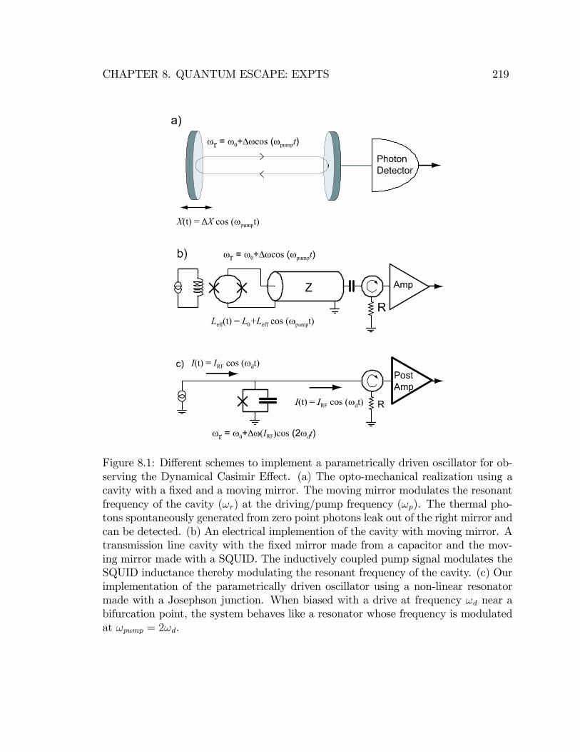
CHAPTER 8. QUANTUM ESCAPE: EXPTS 219
Figure 8.1: Di¤erent schemes to implement a parametrically driven oscillator for ob-serving the Dynamical Casimir E¤ect. (a) The opto-mechanical realization using acavity with a �xed and a moving mirror. The moving mirror modulates the resonantfrequency of the cavity (!r) at the driving/pump frequency (!p). The thermal pho-tons spontaneously generated from zero point photons leak out of the right mirror andcan be detected. (b) An electrical implemention of the cavity with moving mirror. Atransmission line cavity with the �xed mirror made from a capacitor and the mov-ing mirror made with a SQUID. The inductively coupled pump signal modulates theSQUID inductance thereby modulating the resonant frequency of the cavity. (c) Ourimplementation of the parametrically driven oscillator using a non-linear resonatormade with a Josephson junction. When biased with a drive at frequency !d near abifurcation point, the system behaves like a resonator whose frequency is modulatedat !pump = 2!d.
CHAPTER 8. QUANTUM ESCAPE: EXPTS 220
8.1 Dynamical Casimir E¤ect
The paradoxical nature of quantum �uctuations is particularly well showcased in the
Dynamical Casimir E¤ect (DCE)� an elusively weak phenomenon predicted almost
40 years ago [53] but whose theory remains essentially experimentally unveri�ed (see
[102] for a review). In perhaps the most promising opto-mechanical realization of
the DCE [55], one of the mirrors of a Fabry-Perot cavity is driven by a force that
periodically varies the cavity�s geometric length at a frequency !pump which is a mul-
tiple of the lowest cavity mode frequency !0 (see Fig. 8.1a). According to prediction,
even when the cavity is at a low temperature T such that it is initially devoid of all
photons (~!0 >> kBT ) and contains only virtual zero-point quantum �uctuations,
the mirror motion should spontaneously create photons inside the cavity. The e¤ect
is surprising for two reasons: i) no free charge is involved in the radiation process
and ii) entropy appears to be created from a driven, but perfectly ordered system.
These photons obey the statistics of black-body radiation with some e¤ective tem-
perature, i.e., the distribution is thermal. As pointed out by several authors, the
DCE is intimately related with the Unruh e¤ect [103] in cosmology which posits that
vacuum �uctuations appear to an accelerated observer as a thermal bath with an
elevated temperature proportional to the acceleration. The Unruh e¤ect provides a
key semi-classical explanation of black-hole evaporation, and, like the DCE, remains
to be observed. Present experimental techniques lack the required sensitivity for the
unambiguous detection of the DCE by several orders of magnitude, though several
proposals exist [55, 104].
Traditionally, the DCE e¤ect has been discussed in the context of mechanical
motion of a mirror. The use of resonant cavities was introduced to enhance the
CHAPTER 8. QUANTUM ESCAPE: EXPTS 221
photon production rate, with the cavity frequency being modulated by mechanical
means [55]. But if we believe that electrical degrees of freedom are equivalent to
mechanical ones, it is possible to construct an experiment to observe the DCE by
using an electrical resonator. We can periodically vary the frequency of an electrical
resonator not by mechanical means, but through an element whose reactance can be
modulated by an electrical signal. Fig. 8.1b shows a possible implementation using
a SQUID at the end of an electrical cavity. The SQUID inductance and hence the
e¤ective electrical length of the cavity can be varied by coupling a signal inductively.
Fig. 8.1a and Fig. 8.1b are essentially parametrically driven oscillators. As we saw in
the previous chapter, the JBA (8.1c) biased near the bifurcation point behaves like a
parametrically driven oscillator (see section 7.2.1). The JBA converts quantum zero
point �uctuations into thermal �uctuations via parametric ampli�cation. This is the
link between the JBA and the DCE. The traditional DCE e¤ect in cavities can be
thought of as parametric ampli�cation of zero point �uctuations (T = 0) with the
pump being applied to a mechanical degree of freedom. In the JBA, the pump is
applied to an electrical degree of freedom instead. The use of a Josephson junction
based non-linear resonator to observe the DCE has two main advantages. The non-
linearity enables electrical modulation of the resonator frequency while the absence
of dissipation eliminates parasitic channels of heat production.
The DCE predictions and experiments have been mostly concerned with measuring
the e¤ective temperature of the output �eld of the cavity which can be a signi�cant
experimental challenge. An unambiguous detection of the e¤ective temperature of
the photon �eld produced by the DCE requires a detector with minimal coupling
loss and quantum-noise limited sensitivity. The key feature of our experiment is that

CHAPTER 8. QUANTUM ESCAPE: EXPTS 222
we measure the e¤ective temperature of the internal �eld of the resonator. This is
valid because the output �eld and the internal �eld are related to each other (see
section 7.1). As we saw in the previous chapter, the thermal noise created from
the parametric ampli�cation of zero point �uctuations leads to the switching of the
JBA from its low amplitude state to the high amplitude state. By performing a
calibration in the high temperature regime where the switching process is dominated
solely by ordinary black-body thermal radiation, we can infer the temperature of the
spontaneously created noise in the quantum regime and compare it to theory. We
now proceed to describe these escape measurements.
8.2 Quantum escape measurements
8.2.1 Switching measurements in the JBA
The main goal of the experiment is to measure the transitions rates from the low
amplitude to the high amplitude state of the JBA. By characterizing these rates, we
can extract an e¤ective escape temperature TRFesc which is a measure of the intensity
of the �uctuations felt by the system. The escape rate from the low amplitude state
can be written as
�RFesc (IRF ) =!RFa (IRF )
2�exp
� URFesckBTRFesc
�1� I
2RF
I2B
�3=2!(8.1)
where !RFa (IRF ) and URFesc are de�ned in equations 2.32a and 2.33b. I have written
�RFesc (IRF ) as a function of the drive current IRF only since we will be measuring the
CHAPTER 8. QUANTUM ESCAPE: EXPTS 223
variation of escape rate with the drive current. We can rewrite the above equation as
~�RFesc (IRF ) =
�URFesckBTRFesc
�2=3�1� I
2RF
I2B
�(8.2)
where ~�RFesc (IRF ) is a reduced escape rate given by
~�RFesc (IRF ) =
�log
�!RFa (IRF )
2��RFesc (IRF )
��2=3: (8.3)
If we plot ~�RFesc (IRF ) as a function of I2RF , we should get a straight line with a slope
~�slope and an intercept ~�int given by
~�slope = ��URFesckBTRFesc
�2=31
I2B(8.4a)
~�int =
�URFesckBTRFesc
�2=3: (8.4b)
From these two quantities we can determine the bifurcation current IB and escape
temperature TRFesc using the following formulae
IB =��~�int = ~�slope
�1=2(8.5a)
TRFesc =URFesc
kB~�3=2int
(8.5b)
where URFesc is computed using equation 2.33b. So the experiment involves measuring
�RFesc (IRF ) for di¤erent operating parameters and extracting the escape temperature
TRFesc . From the results of the previous chapter, we expect TRFesc to be given by
TRFesc =~!d2kB
coth
�~!d2kBT
�: (8.6)
CHAPTER 8. QUANTUM ESCAPE: EXPTS 224
We studied the variation of TRFesc with bath temperature T and drive frequency !d.
Two JBA samples with a plasma frequency of 1:67 GHz (sample LF) and 4:69 GHz
(sample HF) were measured to study the scaling of TRFesc with frequency.
In order to get an independent calibration of the intensity of �uctuations at every
operating temperature, we measured the escape rates from the superconducting state
to the voltage state of the DC current biased Josephson junction. The theory for
this experiment is well understood and has been experimentally veri�ed to be quite
accurate [48]. The escape rate for this process is given by
�DCesc (IDC) = ap!p2�(1� IDC=I0)1=4 exp
�4p2
3
EJkBTDCesc
�1� IDC
I0
�3=2!
where I0 is the critical current of the junction, EJ = '0I0 is the Josephson energy, !p is
the plasma frequency and ap is a prefactor of order unity to account for �nite damping.
Using the procedure described above, we can extract the escape temperature TDCesc by
measuring �DCesc (IDC). In our experiments, we were always in the classical regime
(kBT & ~!p (1� IDC=I0)1=4 =2�) where TDCesc = T , the bath temperature.
8.2.2 Combined RF and DC biasing scheme
One of the main challenges of this experiment was to implement an ultra low noise
biasing scheme. We want the JBA to only feel the thermal/quantum �uctuations
corresponding to the bath temperature T at which the experiment is carried out.
The ability to measure DC and RF switching in the same experimental setup adds
to the complication. The best DC biasing schemes are implemented using shielded,
twisted-pair wires which are excited di¤erentially. This not only eliminates interaction

CHAPTER 8. QUANTUM ESCAPE: EXPTS 225
Figure 8.2: A schematic of the biasing scheme for combining singled-ended RF withdi¤erential DC signals. Shielded twisted-pair wires are used to carry out a four wireDC I � V measurement. A 180 degree hybrid is used to split the RF signal intotwo components which are phase shifted by 180 degrees, creating the di¤erential RFdrive. The RF and DC signals are combined using a "Bias Tee" before they reachthe device (inside blue box). A superconducting (at T = 12 mK) aluminum box isused to shield the device from low frequency magnetic �elds since the twisted-pairshave to be opened up before they can combined with the RF signals. This di¤erentialbiasing scheme allows the creation of an ultra-low noise environment for the deviceat both low and high frequencies.
CHAPTER 8. QUANTUM ESCAPE: EXPTS 226
with the ground of the electrical system which is often noisy, but also minimizes
inductive pickup. RF signals are typically propagated on single ended coaxial lines
and since they can be capacitively coupled, grounding problems are usually not an
issue. In order to combine the di¤erential DC and single-ended RF bias lines we
had to transform the RF signal into a di¤erential one using a device called the 180
degree hybrid. Now we have two single ended RF signals with opposite phase and
each part is combined with the DC signal from the two wires of the twisted-pair
respectively. This is the most vulnerable part of the biasing circuit since the twisted-
pair now opens up into a loop and therefore prone to low frequency inductive pickup.
A superconducting (at T = 12 mK) aluminum box was used to shield this part of
the circuit from low frequency magnetic �elds. The combined signals then go to the
device enabling di¤erential excitation. The biasing scheme is shown schematically in
Fig. 8.2.
The �lter chain for the DC path (both current and voltage lines) included several
copper powder �lters made with twisted-pair wires for �ltering high frequency noise
(& 1 GHz). Pi �lters made with inductors and capacitors were used to �lter the
intermediate frequency noise and limit the bandwidth of the DC lines to about 10
kHz. In addition, for the current line, a 100:1 voltage divider at the 4K stage of the
fridge and a well thermalized bias resistor at the base temperature stage were used.
For the RF lines, the �lter chain on the input side included several attenuators (� 73
dB total) and re�ective �lters to set a pass band from 1 to 2 GHz for sample LF and
4 to 5 GHz for sample HF. The RF �lter chain for the output line was made up of
three circulators with two of them anchored at the base temperature and one at the
100 mK stage of the dilution refrigerator. A very important element of the RF output

CHAPTER 8. QUANTUM ESCAPE: EXPTS 227
Figure 8.3: A picture of the base temperature stage of the experiment showing thesuperconducting aluminum box containing the DC and RF circuitry.
line was the lossy low pass �lter. This �lter is basically a microstrip transmission line
where the dielectric has a frequency dependent loss. The main advantage of these
�lters is that they are well matched to the 50 ohm transmission lines thereby avoiding
re�ections and the possibility of setting up standing waves. The �ltering action comes
from a frequency dependent attenuation of the signal passing through. These can be
designed to have less than 1 dB attenuation in the pass band (< 2 GHz). The loss
outside the pass band can be as large as 60 dB. See [66] for more details. Fig. 8.3
shows an image of the aluminum box with DC and RF circuitry inside.
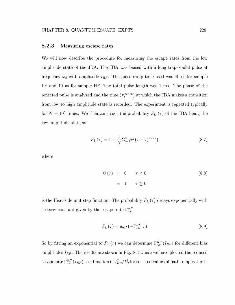
CHAPTER 8. QUANTUM ESCAPE: EXPTS 228
8.2.3 Measuring escape rates
We will now describe the procedure for measuring the escape rates from the low
amplitude state of the JBA. The JBA was biased with a long trapezoidal pulse at
frequency !d with amplitude IRF . The pulse ramp time used was 40 ns for sample
LF and 10 ns for sample HF. The total pulse length was 1 ms. The phase of the
re�ected pulse is analyzed and the time (� switchi ) at which the JBA makes a transition
from low to high amplitude state is recorded. The experiment is repeated typically
for N = 105 times. We then construct the probability PL (�) of the JBA being the
low amplitude state as
PL (�) = 1�1
N�Ni=1�
�� � � switchi
�(8.7)
where
�(�) = 0 � < 0 (8.8)
= 1 � � 0
is the Heaviside unit step function. The probability PL (�) decays exponentially with
a decay constant given by the escape rate �RFesc
PL (�) = exp���RFesc �
�(8.9)
So by �tting an exponential to PL (�) we can determine �RFesc (IRF ) for di¤erent bias
amplitudes IRF . The results are shown in Fig. 8.4 where we have plotted the reduced
escape rate ~�RFesc (IRF ) as a function of I2RF=I
2B for selected values of bath temperatures.
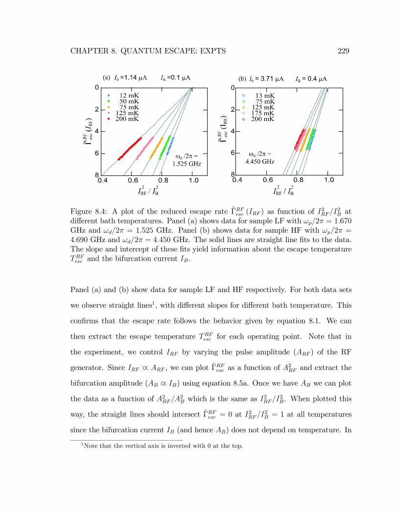
CHAPTER 8. QUANTUM ESCAPE: EXPTS 229
Figure 8.4: A plot of the reduced escape rate ~�RFesc (IRF ) as function of I2RF=I
2B at
di¤erent bath temperatures. Panel (a) shows data for sample LF with !p=2� = 1:670GHz and !d=2� = 1:525 GHz. Panel (b) shows data for sample HF with !p=2� =4:690 GHz and !d=2� = 4:450 GHz. The solid lines are straight line �ts to the data.The slope and intercept of these �ts yield information about the escape temperatureTRFesc and the bifurcation current IB.
Panel (a) and (b) show data for sample LF and HF respectively. For both data sets
we observe straight lines1, with di¤erent slopes for di¤erent bath temperature. This
con�rms that the escape rate follows the behavior given by equation 8.1. We can
then extract the escape temperature TRFesc for each operating point. Note that in
the experiment, we control IRF by varying the pulse amplitude (ARF ) of the RF
generator. Since IRF _ ARF , we can plot ~�RFesc as a function of A2RF and extract the
bifurcation amplitude (AB _ IB) using equation 8.5a. Once we have AB we can plot
the data as a function of A2RF=A2B which is the same as I
2RF=I
2B. When plotted this
way, the straight lines should intersect ~�RFesc = 0 at I2RF=I
2B = 1 at all temperatures
since the bifurcation current IB (and hence AB) does not depend on temperature. In
1Note that the vertical axis is inverted with 0 at the top.

CHAPTER 8. QUANTUM ESCAPE: EXPTS 230
practice, we always observe small di¤erences in the extracted values of AB at di¤erent
temperatures. This could imply that the data starts to deviate from the prediction
of equation 8.1. But we found that this variation was predominantly due to the
slow increase in the attenuation of the input coaxial lines due to slowly decreasing
levels of liquid Helium in the dewar of the dilution refrigerator. We observed that the
extracted values of AB always increased with time even when the temperature was
kept constant and reverts back when the liquid Helium level is restored. The data
shown in Fig. 8.4 takes about 2 days to acquire since one has to wait for the system
to thermalize at each operating temperature. During such long periods, the liquid
Helium level can change appreciably. We also veri�ed that the extracted values of
AB remained constant when noise was added to the system to arti�cially elevate the
temperature. All these checks were done to ensure that our experiment really follows
the prediction of equation 8.1 and we can extract meaningful results for the value of
TRFesc . The data for each temperature in Fig. 8.4 has been plotted after normalizing
the x-axis with the value of IB (AB) extracted at the lowest temperature so that the
variations in IB (AB) are still visible.
8.2.4 Temperature dependence
In order to extract TRFesc from the data, we need the value of URFesc . Data from numerical
simulations2 of the JBA circuit yielded a value for URFesc which was 10-20% than those
obtained from equation 2.33b. This would lead to a 10-20% smaller value for TRFesc
and we observed this discrepancy in the experiments. In order to overcome this
problem, we used the following procedure. At the highest temperature point, we
2The numerical simulations were used to compute escape rates in the JBA. Since we know theprecise temperature (T ) used in the simulations, we can extract URFesc by setting T
RFesc = T .

CHAPTER 8. QUANTUM ESCAPE: EXPTS 231
Figure 8.5: A plot of TDCesc vs T in a DC current biased Josephson junction. Datafor sample LF with !p=2� = 1:670 GHz is shown in red while that for sample HFwith !p=2� = 4:690 GHz is shown in blue. The dashed line is expected dependenceTDCesc = T . The data falls on the dashed line for high temperatures but TDCesc startsto saturate at the low temperature. We believe the small deviations are due toimproperly thermalized �lters and un�ltered noise in the dual biasing con�guration.The high frequency dynamics at the bare plasma frequency (� 20GHz) of the junctioncan also contribute to this e¤ect.
assumed TRFesc = T , since that is the expected result in the classical regime. We can
then use equation 8.5b to extract URFesc = kBTRFesc~�3=2int . This extracted value of U
RFesc is
then used for all the lower temperature points. This is valid provided we can ensure
that the intensity of �uctuations felt by the JBA really corresponds to the thermal
�uctuations at temperature T . We veri�ed this by biasing the junction with a DC
current and measuring the escape rate from the superconducting to the normal state
of the junction. We used the procedure3 described in ref. [48] to measure the escape
3The measurement protocol is basically the same as the one for JBA switching but we use alinear ramp instead of a trapezoidal pulse. This slightly changes the procedure for extracting theescape rate from the data.
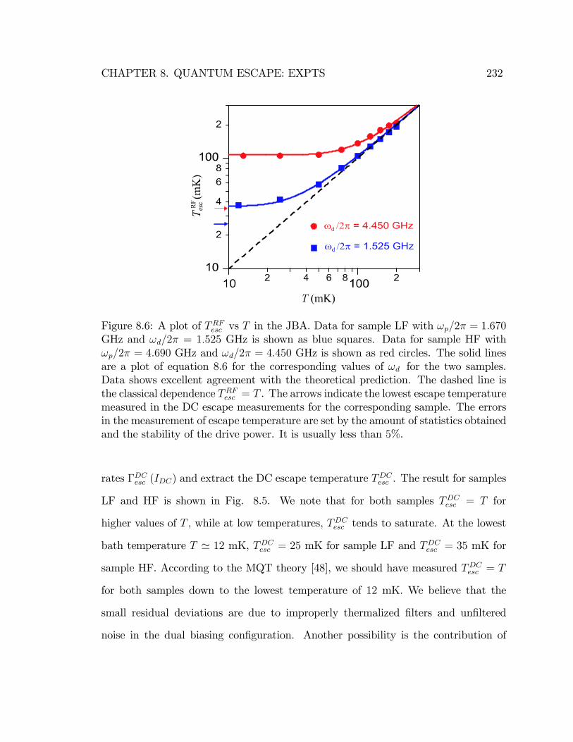
CHAPTER 8. QUANTUM ESCAPE: EXPTS 232
Figure 8.6: A plot of TRFesc vs T in the JBA. Data for sample LF with !p=2� = 1:670GHz and !d=2� = 1:525 GHz is shown as blue squares. Data for sample HF with!p=2� = 4:690 GHz and !d=2� = 4:450 GHz is shown as red circles. The solid linesare a plot of equation 8.6 for the corresponding values of !d for the two samples.Data shows excellent agreement with the theoretical prediction. The dashed line isthe classical dependence TRFesc = T . The arrows indicate the lowest escape temperaturemeasured in the DC escape measurements for the corresponding sample. The errorsin the measurement of escape temperature are set by the amount of statistics obtainedand the stability of the drive power. It is usually less than 5%.
rates �DCesc (IDC) and extract the DC escape temperature TDCesc . The result for samples
LF and HF is shown in Fig. 8.5. We note that for both samples TDCesc = T for
higher values of T , while at low temperatures, TDCesc tends to saturate. At the lowest
bath temperature T ' 12 mK, TDCesc = 25 mK for sample LF and TDCesc = 35 mK for
sample HF. According to the MQT theory [48], we should have measured TDCesc = T
for both samples down to the lowest temperature of 12 mK. We believe that the
small residual deviations are due to improperly thermalized �lters and un�ltered
noise in the dual biasing con�guration. Another possibility is the contribution of
CHAPTER 8. QUANTUM ESCAPE: EXPTS 233
high frequency dynamics at the bare plasma frequency of the Josephson junction.
This can happen due to the �nite stray inductance between the junction and the
microfabricated shunting capacitor (see section 3.2.1). Nevertheless, the DC escape
temperature data validates our normalization procedure described in the previous
paragraph.
Fig. 8.6 plots TRFesc extracted from the data shown in Fig. 8.4 as a function of
bath temperature T for both samples. The solid lines are a plot of equation 8.6 with
the corresponding values of !d used for the two samples. The agreement between
theory and experiment is excellent. Note that this is not a �t to the data. The
only scaling of data performed, as explained above, is the extraction of URFesc from
the highest temperature data point for each sample. The results for TRFesc not only
agree with theory for the lowest temperature point, but the functional dependence
on temperature as we cross-over from the classical (kBT >> ~!d) to quantum regime
(kBT << ~!d) is also nicely reproduced.
8.2.5 Detuning dependence
We also studied the variation of TRFesc as function of drive frequency !d for each sample
separately. Since the range of drive frequencies accessible for a given sample is small
(!d � !p), we expect that the saturation temperature TRFesc (T ! 0) = ~!d=2kB is
roughly constant for each sample. Fig. 8.7 shows a plot of TRFesc (T ! 0) as a function
of !d=2� for both samples. Data for sample LF (blue circles) show a fairly constant
value of the saturation temperature which is in good agreement with the theoretical
prediction (blue dashed line). However, the data for sample HF (red circles) shows a
much stronger variation in the saturation temperature. The agreement with theory is
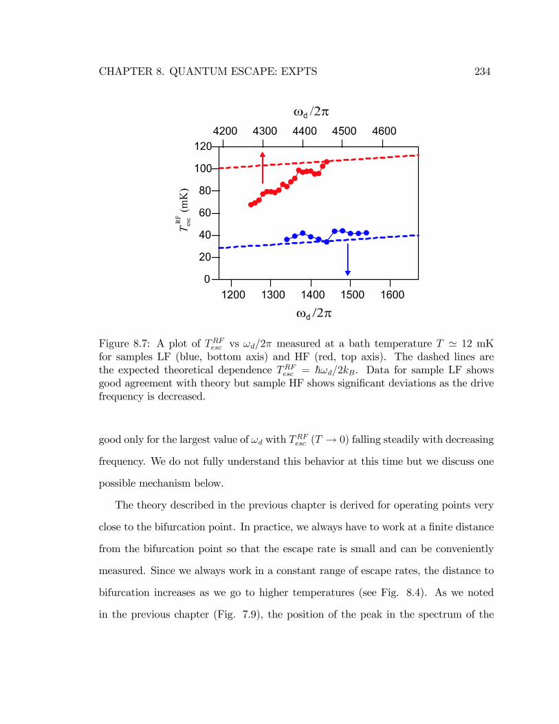
CHAPTER 8. QUANTUM ESCAPE: EXPTS 234
Figure 8.7: A plot of TRFesc vs !d=2� measured at a bath temperature T ' 12 mKfor samples LF (blue, bottom axis) and HF (red, top axis). The dashed lines arethe expected theoretical dependence TRFesc = ~!d=2kB. Data for sample LF showsgood agreement with theory but sample HF shows signi�cant deviations as the drivefrequency is decreased.
good only for the largest value of !d with TRFesc (T ! 0) falling steadily with decreasing
frequency. We do not fully understand this behavior at this time but we discuss one
possible mechanism below.
The theory described in the previous chapter is derived for operating points very
close to the bifurcation point. In practice, we always have to work at a �nite distance
from the bifurcation point so that the escape rate is small and can be conveniently
measured. Since we always work in a constant range of escape rates, the distance to
bifurcation increases as we go to higher temperatures (see Fig. 8.4). As we noted
in the previous chapter (Fig. 7.9), the position of the peak in the spectrum of the
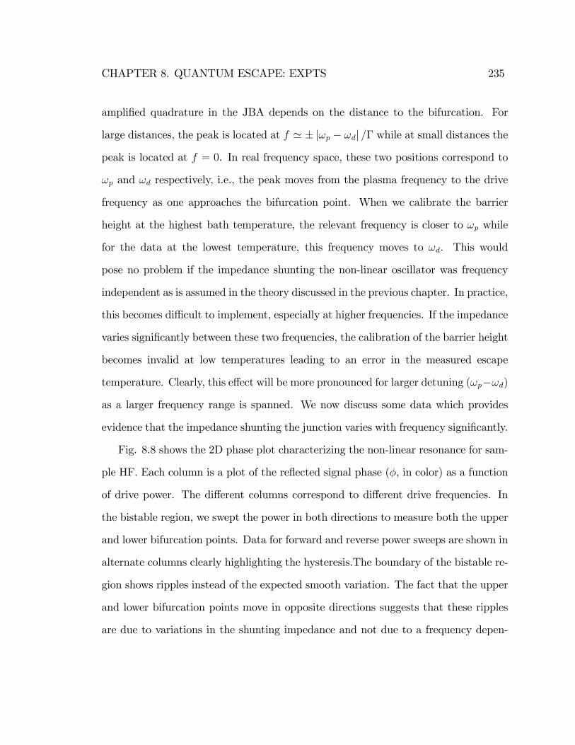
CHAPTER 8. QUANTUM ESCAPE: EXPTS 235
ampli�ed quadrature in the JBA depends on the distance to the bifurcation. For
large distances, the peak is located at f ' � j!p � !dj =� while at small distances the
peak is located at f = 0. In real frequency space, these two positions correspond to
!p and !d respectively, i.e., the peak moves from the plasma frequency to the drive
frequency as one approaches the bifurcation point. When we calibrate the barrier
height at the highest bath temperature, the relevant frequency is closer to !p while
for the data at the lowest temperature, this frequency moves to !d. This would
pose no problem if the impedance shunting the non-linear oscillator was frequency
independent as is assumed in the theory discussed in the previous chapter. In practice,
this becomes di¢ cult to implement, especially at higher frequencies. If the impedance
varies signi�cantly between these two frequencies, the calibration of the barrier height
becomes invalid at low temperatures leading to an error in the measured escape
temperature. Clearly, this e¤ect will be more pronounced for larger detuning (!p�!d)
as a larger frequency range is spanned. We now discuss some data which provides
evidence that the impedance shunting the junction varies with frequency signi�cantly.
Fig. 8.8 shows the 2D phase plot characterizing the non-linear resonance for sam-
ple HF. Each column is a plot of the re�ected signal phase (�, in color) as a function
of drive power. The di¤erent columns correspond to di¤erent drive frequencies. In
the bistable region, we swept the power in both directions to measure both the upper
and lower bifurcation points. Data for forward and reverse power sweeps are shown in
alternate columns clearly highlighting the hysteresis.The boundary of the bistable re-
gion shows ripples instead of the expected smooth variation. The fact that the upper
and lower bifurcation points move in opposite directions suggests that these ripples
are due to variations in the shunting impedance and not due to a frequency depen-
CHAPTER 8. QUANTUM ESCAPE: EXPTS 236
Figure 8.8: A 2D phase plot characterizing the non-linear resonance for sample HF.Each column is a plot of the re�ected signal phase (�, in color) as a function ofdrive power (P=Pc). Pc is the critical drive power. The di¤erent columns correspondto di¤erent drive frequencies. In the bistable region, we swept the power in bothdirections to measure both the upper and lower bifurcation points. Data for forwardand reverse power sweeps are shown in alternate columns clearly highlighting thehysteresis. Also visible are ripples in the boundary marking the bistable region,indicating variations in the impedance shunting the JBA.
dent power coupling which would have caused them to move in the same direction.
The width of the hysteresis is proportional to the real part of the impedance4 at that
frequency. The use of the hybrid to implement the di¤erential RF biasing scheme can
lead to this impedance variation. The electric length of the two paths from the hybrid
to the junction have to be kept as identical as possible. Any asymmetry in the two
paths can lead to variations in the impedance seen by the junction. This is di¢ cult
to implement especially at higher frequencies. The 2D phase plot shown in Fig. 3.6
4The width of the hysteris is proportional to the relative detuning � and the quality factor Q ofthe resonator. The dependence on � is smooth so any ripples in the hysteresis width has to do withlocal variations in Q or the real part of the impedance at that frequency. See also ref. [59].

CHAPTER 8. QUANTUM ESCAPE: EXPTS 237
and all other samples we measured without the di¤erential biasing scheme showed no
ripples in the width of the hysteresis. Sample LF also showed some variations in the
shunting impedance which is re�ected in the ripples in the measured TRFesc as seen in
Fig. 8.7, though the e¤ect here is much smaller.
At this stage, we believe that the disagreement with theory for sample HF is
predominantly due to the impedance variations, though we cannot completely rule out
other e¤ects not included in the theory described in the previous chapter. For future
experiments, we hope to solve this impedance variation problem by implementing the
non-linear oscillator using geometric resonators which would provide a much better
control over the impedance shunting the junction.
8.3 Parametric ampli�cation in the JBA
We now describe some preliminary experiments which test the performance of the
JBA as a parametric ampli�er (PARAMP). These are proof of principle experiments
and have not yet been optimized for practical applications.
8.3.1 Measurement protocol
The measurement protocol is as follows. We energize the JBA with a CW signal at
frequency !d close to the critical point. This signal is known as the pump. To this
pump, we add another input at frequency !s which is much weaker than the pump.
This is called the signal. As explained in section 7.3, the re�ected output from the
PARAMP contains an ampli�ed component of the signal at !s along with another
component called the idler at !i = 2!d � !s. Fig. 8.9a shows a schematic of the
measurement protocol while 8.9b shows the pump, signal and idler components in the
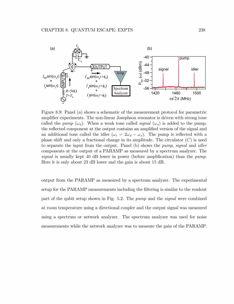
CHAPTER 8. QUANTUM ESCAPE: EXPTS 238
Figure 8.9: Panel (a) shows a schematic of the measurement protocol for parametricampli�er experiments. The non-linear Josephson resonator is driven with strong tonecalled the pump (!d). When a weak tone called signal (!s) is added to the pump,the re�ected component at the output contains an ampli�ed version of the signal andan additional tone called the idler (!i = 2!d � !s). The pump is re�ected with aphase shift and only a fractional change in its amplitude. The circulator (C) is usedto separate the input from the output. Panel (b) shows the pump, signal and idlercomponents at the output of a PARAMP as measured by a spectrum analyzer. Thesignal is usually kept 40 dB lower in power (before ampli�cation) than the pump.Here it is only about 23 dB lower and the gain is about 15 dB.
output from the PARAMP as measured by a spectrum analyzer. The experimental
setup for the PARAMP measurements including the �ltering is similar to the readout
part of the qubit setup shown in Fig. 5.2. The pump and the signal were combined
at room temperature using a directional coupler and the output signal was measured
using a spectrum or network analyzer. The spectrum analyzer was used for noise
measurements while the network analyzer was to measure the gain of the PARAMP.

CHAPTER 8. QUANTUM ESCAPE: EXPTS 239
8.3.2 Gain and noise temperature
We used the following procedure to measure the gain of the PARAMP. Using a net-
work analyzer, we �rst measured the transmission through the entire measurement
chain but with the pump o¤. In the absence of the pump, the JBA behaves like a
harmonic oscillator for a weak input. Since the intrinsic dissipation in the JBA is very
small, it re�ects the entire signal back, i.e., the gain is unity. We then repeat the same
measurement with the pump on and divide the result by the �rst measurement. This
directly gives us the gain of the PARAMP. We always ensure that the strength of the
signal is 40 dB lower in power than the pump to prevent saturating the PARAMP.
We do the same two measurements for determining the noise performance but record
the output power spectrum using a spectrum analyzer. The ratio of the two noise
spectrums gives us information about the noise added by the PARAMP.
Fig. 8.10 shows the gain as well as the noise spectrum (with pump on and o¤)
for an operating point close to the critical point. Note that the gain is maximum at
the pump frequency (1450 MHz) and is greater than 25 dB. The spurious peak at
1450 MHz in the noise spectrum is the remnant of the pump signal which we tried to
cancel by adding a coherent tone to the output at the pump frequency. The unwanted
pump signal at the output of the PARAMP within its band is one of the drawbacks of
this mode of operation. In the next chapter, we will brie�y outline a new, Josephson
junction based ampli�er which overcomes this problem.
Fig. 8.11 shows a plot of the power gain (color) of the PARAMP as a function of
signal frequency and pump power. The pump frequency used was 1450 MHz. This
plot qualitatively agrees with the predicted gain shown in Fig. 7.10 with regions of
single and double peaks in the gain as a function of frequency. An important di¤erence

CHAPTER 8. QUANTUM ESCAPE: EXPTS 240
Figure 8.10: Gain (right axis )and noise measurements (left axis) in a PARAMP.Pump frequency is 1450 MHz and the pump power is adjusted for maximum gain.We note a maximum gain of about 27 dB at 1450 MHz which is the pump frequency.Output noise as measured by a spectrum analyzer is plotted in black (pump o¤) andred (pump on). The increase in noise with the pump on tells us about the noise addedin the ampli�cation process. The spurious peak at 1450 MHz in the noise spectrumis the remnant of the pump signal which we tried to cancel by adding a coherent toneto the output at the pump frequency
we note is that the gain is not perfectly symmetric about the pump frequency as
predicted by theory. This is due to the assumption in the theory that the resonator
has no intrinsic dissipation. If we include additional sources of dissipation, the gain
becomes asymmetric [101]. Also note how the bandwidth increases with decreasing
gain. This is a common feature of PARAMPS. Nevertheless, we can see that it is
possible to get about 50 MHz of bandwidth with a gain of about 15 dB.
We will now describe how to extract the noise temperature of the PARAMP. We
will call the frequency dependent power gain of the PARAMP as GP (!) and its
noise temperature TNP (!). In what follows, we will express the noise power as a
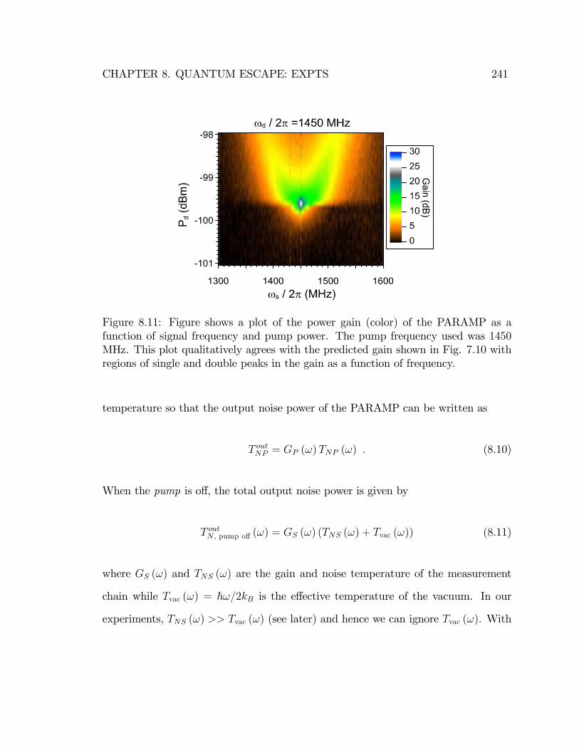
CHAPTER 8. QUANTUM ESCAPE: EXPTS 241
Figure 8.11: Figure shows a plot of the power gain (color) of the PARAMP as afunction of signal frequency and pump power. The pump frequency used was 1450MHz. This plot qualitatively agrees with the predicted gain shown in Fig. 7.10 withregions of single and double peaks in the gain as a function of frequency.
temperature so that the output noise power of the PARAMP can be written as
T outNP = GP (!)TNP (!) : (8.10)
When the pump is o¤, the total output noise power is given by
T outN , pump o¤ (!) = GS (!) (TNS (!) + Tvac (!)) (8.11)
where GS (!) and TNS (!) are the gain and noise temperature of the measurement
chain while Tvac (!) = ~!=2kB is the e¤ective temperature of the vacuum. In our
experiments, TNS (!) >> Tvac (!) (see later) and hence we can ignore Tvac (!). With

CHAPTER 8. QUANTUM ESCAPE: EXPTS 242
the pump on, we get
T outN , pump on (!) = GS (!)ToutNP (!) +GS (!)TNS (!) : (8.12)
Taking the ratio of the two and diving by the gain of the PARAMP, we get,
T outN , pump on (!)
GP (!)T outN , pump o¤ (!)= TN ,ratio = 1 +
TNP (!)
TNS (!): (8.13)
Since we can measureGP (!) and the ratio T outN , pump on (!) =ToutN , pump o¤ (!) as described
above, we can compute TN ,ratio. We can then determine TNP (!) from the above equa-
tion if we know TNS (!). Accurately determining the system noise temperature of a
cryogenic setup is quite challenging and requires a well calibrated variable temper-
ature load or a calibrated noise source which works at cryogenic temperatures. We
were only able to make a rough measurement of the system noise temperature by
varying the temperature of the base temperature stage of our cryostat, and estimated
it to be TNS ' 12 K �20% within the frequency band of our experiment (1:3-1:5
GHz) . This number agreed with our estimate using the manufacture provided num-
ber for the noise temperature of the HEMT ampli�er (2:2 K) and about 6 dB of loss
in our output line from the sample to the HEMT ampli�er. This limits our accuracy
to determine the noise temperature of the PARAMP to �20%.
Fig. 8.12 shows plots of the gain and noise temperature (in color) as a function
of signal frequency and pump frequency. The pump power at each value of pump
frequency has been optimized for maximum gain. In panel (b), one should ignore
the blue region on either side as it does not represent valid data. Also, the noise
temperature data becomes noisy as one moves away from the pump frequency due
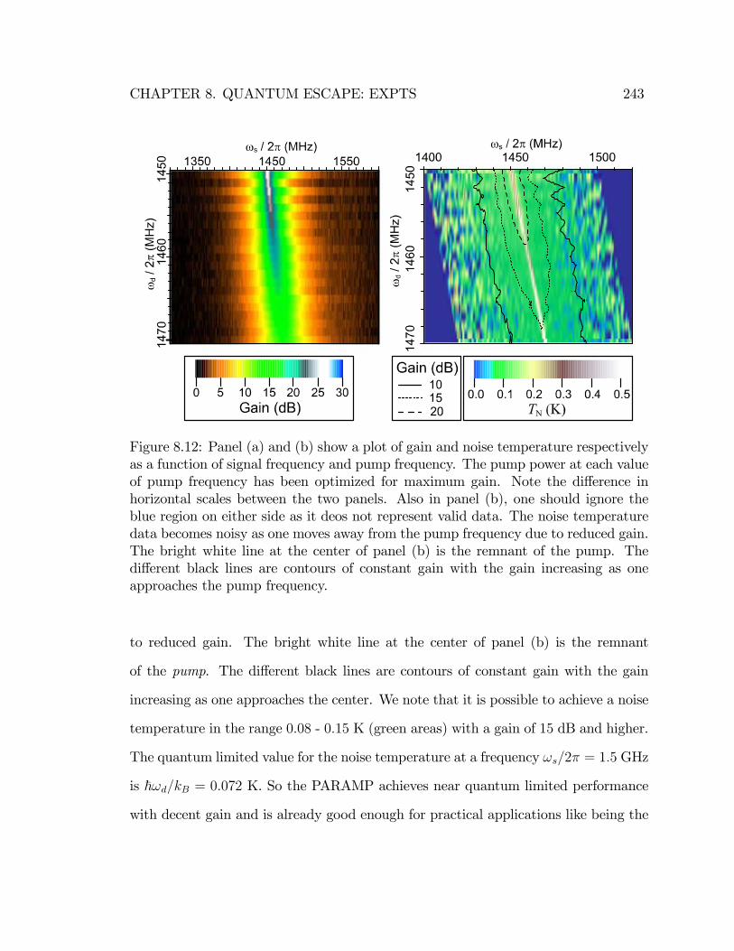
CHAPTER 8. QUANTUM ESCAPE: EXPTS 243
Figure 8.12: Panel (a) and (b) show a plot of gain and noise temperature respectivelyas a function of signal frequency and pump frequency. The pump power at each valueof pump frequency has been optimized for maximum gain. Note the di¤erence inhorizontal scales between the two panels. Also in panel (b), one should ignore theblue region on either side as it deos not represent valid data. The noise temperaturedata becomes noisy as one moves away from the pump frequency due to reduced gain.The bright white line at the center of panel (b) is the remnant of the pump. Thedi¤erent black lines are contours of constant gain with the gain increasing as oneapproaches the pump frequency.
to reduced gain. The bright white line at the center of panel (b) is the remnant
of the pump. The di¤erent black lines are contours of constant gain with the gain
increasing as one approaches the center. We note that it is possible to achieve a noise
temperature in the range 0:08 - 0:15 K (green areas) with a gain of 15 dB and higher.
The quantum limited value for the noise temperature at a frequency !s=2� = 1:5 GHz
is ~!d=kB = 0:072 K. So the PARAMP achieves near quantum limited performance
with decent gain and is already good enough for practical applications like being the
CHAPTER 8. QUANTUM ESCAPE: EXPTS 244
�rst stage ampli�er for experiments like dispersive qubit measurements. Though the
strong pump signal still needs to be isolated from the qubit using isolators. Section
9.3 discusses a modi�ed design to solve this problem.
8.3.3 Squeezing measurements
Squeezing of thermal and vacuum noise has been demonstrated in Josephson junction
based parametric ampli�ers [105, 25]. We discuss below some preliminary experiments
testing the ability of the JBA to squeeze vacuum noise (T << ~!d=kB). The mea-
surement protocol is similar to the one described in 8.3.1 but now we beat the output
signal with another signal at the pump frequency !d using a mixer. The beating
signal is phase locked with the pump. The output of the mixer is �ltered to remove
the high frequency components and fed to a spectrum analyzer. We now look at the
spectrum near zero frequency. We �rst looked at the case when a signal tone at !s
was present along with the pump at !d. The mixer combines the signals at !s and
!i = 2!d�!s and outputs them at a frequency j!d � !sj. The spectrum at j!d � !sj
is monitored as a function of the phase di¤erence (�LO) between the pump and the
beating signal. The result is shown in Fig. 8.13a. The black curve corresponds to
the pump being o¤ and shows no dependence on �LO while the red curve taken with
the pump on shows strong variations. At certain values of �LO, the red curve falls
below the black curve implying a destructive interference between the components at
!s and !i. When the same thing happens with the noise, it is called squeezing and
is shown in Fig. 8.13b.
Though the e¤ect is small we can clearly see the red curve dipping just below the
black curve which corresponds to the vacuum �oor. The squeezing e¤ect in the output
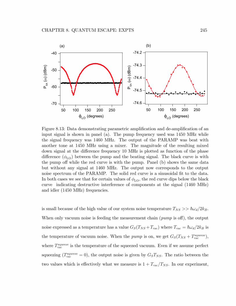
CHAPTER 8. QUANTUM ESCAPE: EXPTS 245
Figure 8.13: Data demonstrating parametric ampli�cation and de-ampli�cation of aninput signal is shown in panel (a). The pump frequency used was 1450 MHz whilethe signal frequency was 1460 MHz. The output of the PARAMP was beat withanother tone at 1450 MHz using a mixer. The magnitude of the resulting mixeddown signal at the di¤erence frequency 10 MHz is plotted as function of the phasedi¤erence (�LO) between the pump and the beating signal. The black curve is withthe pump o¤ while the red curve is with the pump. Panel (b) shows the same databut without any signal at 1460 MHz. The output now corresponds to the outputnoise spectrum of the PARAMP. The solid red curve is a sinusoidal �t to the data.In both cases we see that for certain values of �LO, the red curve dips below the blackcurve indicating destructive interference of components at the signal (1460 MHz)and idler (1450 MHz) frequencies.
is small because of the high value of our system noise temperature TNS >> ~!d=2kB.
When only vacuum noise is feeding the measurement chain (pump is o¤), the output
noise expressed as a temperature has a value GS(TNS+Tvac) where Tvac = ~!d=2kB is
the temperature of vacuum noise. When the pump is on, we get GS(TNS + T squeezevac ),
where T squeezevac is the temperature of the squeezed vacuum. Even if we assume perfect
squeezing (T squeezevac = 0), the output noise is given by GSTNS. The ratio between the
two values which is e¤ectively what we measure is 1 + Tvac=TNS. In our experiment,

CHAPTER 8. QUANTUM ESCAPE: EXPTS 246
Tvac=TNS ' 0:003 << 1, and hence the squeezing e¤ect in the output is very small.
We now provide a rough estimate of the amount squeezing achieved. From the noise
temperature measurements, our best estimate of Tvac=TNS � 0:004. The red curve
dips below the black curve in Fig. 8.13b by about 0:026 � 0:008 dB. We can then
estimate the amount of squeezing T squeezevac =Tvac. Unfortunately the error in the noise
measurements (estimated from the spread in the black data points) is so large that
the estimated amount of squeezing goes all the way from 10% to better than 100%
squeezing (which is not possible). At this point, we would just like to say that we
observe some evidence of squeezing but further improvements in the system noise
temperature and the precision of noise measurements are required to estimate the
amount of squeezing more precisely.
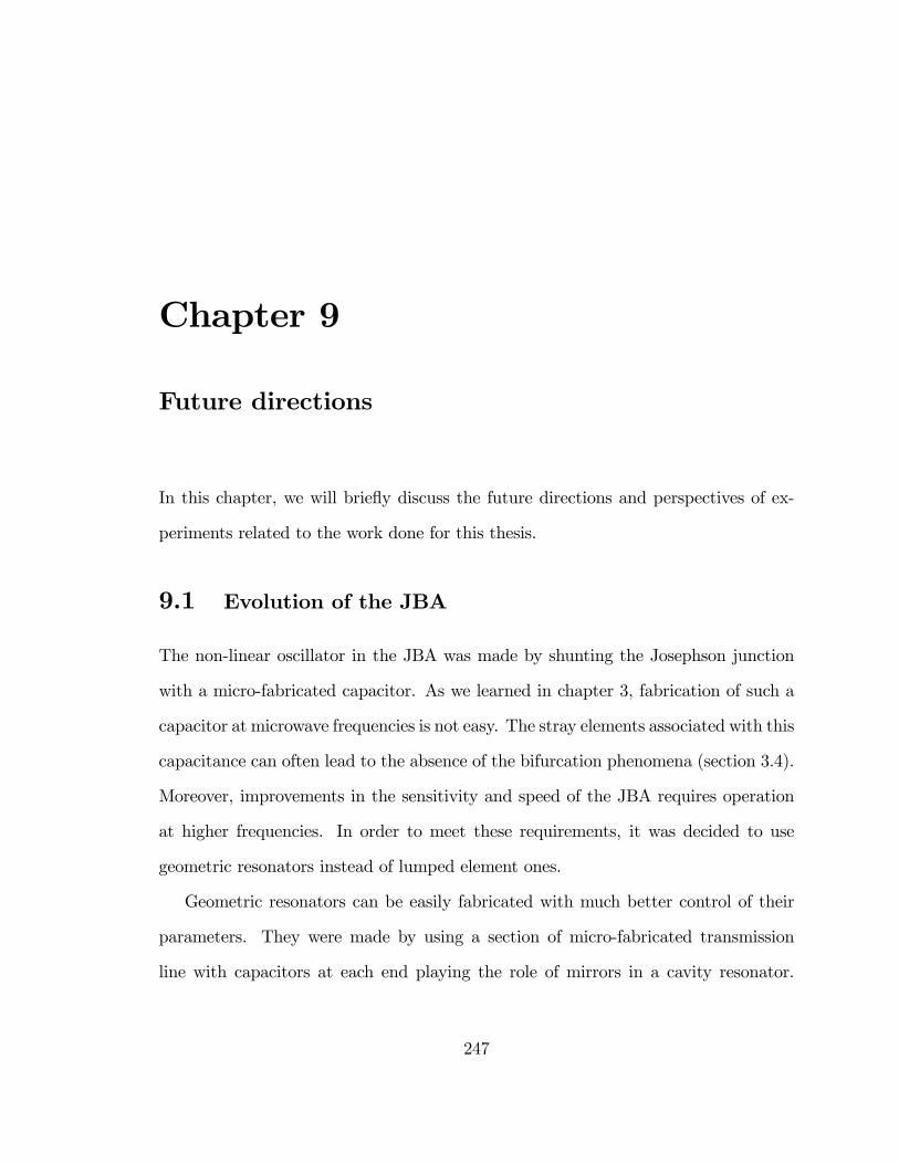
Chapter 9
Future directions
In this chapter, we will brie�y discuss the future directions and perspectives of ex-
periments related to the work done for this thesis.
9.1 Evolution of the JBA
The non-linear oscillator in the JBA was made by shunting the Josephson junction
with a micro-fabricated capacitor. As we learned in chapter 3, fabrication of such a
capacitor at microwave frequencies is not easy. The stray elements associated with this
capacitance can often lead to the absence of the bifurcation phenomena (section 3.4).
Moreover, improvements in the sensitivity and speed of the JBA requires operation
at higher frequencies. In order to meet these requirements, it was decided to use
geometric resonators instead of lumped element ones.
Geometric resonators can be easily fabricated with much better control of their
parameters. They were made by using a section of micro-fabricated transmission
line with capacitors at each end playing the role of mirrors in a cavity resonator.
247
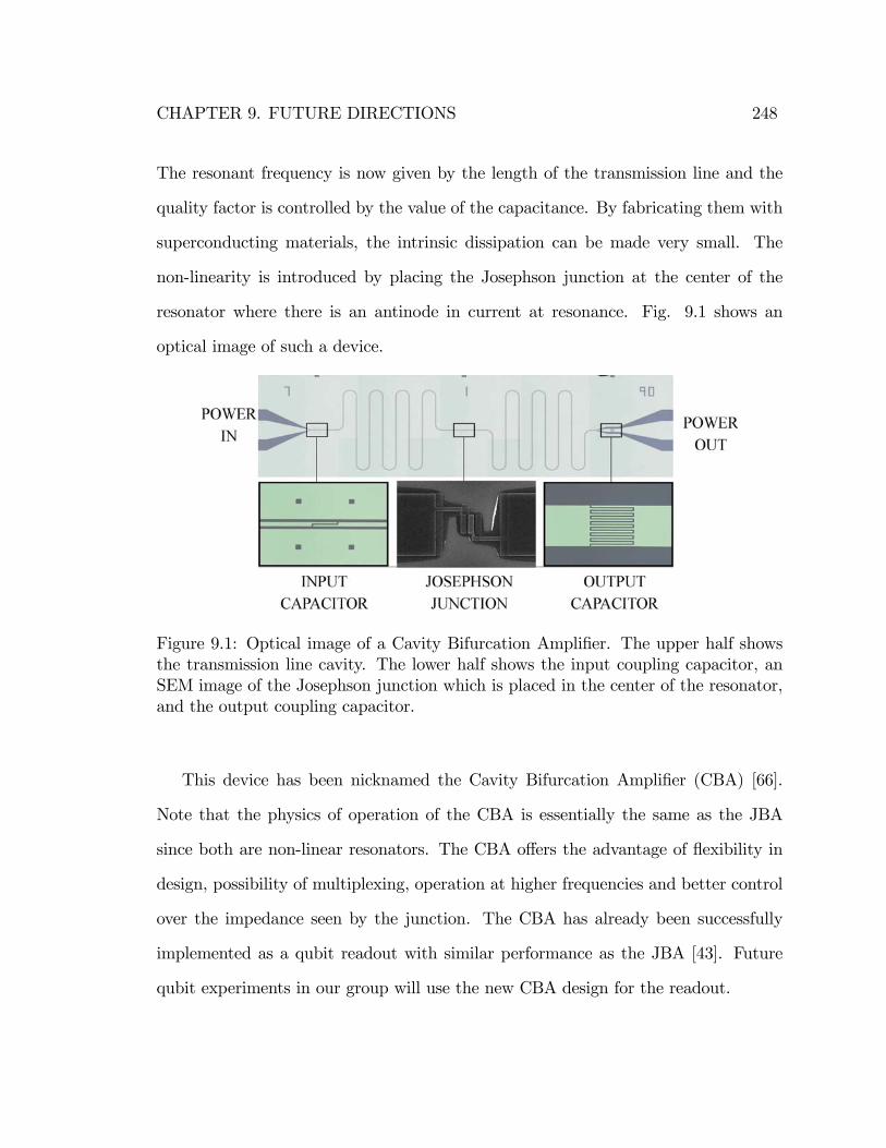
CHAPTER 9. FUTURE DIRECTIONS 248
The resonant frequency is now given by the length of the transmission line and the
quality factor is controlled by the value of the capacitance. By fabricating them with
superconducting materials, the intrinsic dissipation can be made very small. The
non-linearity is introduced by placing the Josephson junction at the center of the
resonator where there is an antinode in current at resonance. Fig. 9.1 shows an
optical image of such a device.
Figure 9.1: Optical image of a Cavity Bifurcation Ampli�er. The upper half showsthe transmission line cavity. The lower half shows the input coupling capacitor, anSEM image of the Josephson junction which is placed in the center of the resonator,and the output coupling capacitor.
This device has been nicknamed the Cavity Bifurcation Ampli�er (CBA) [66].
Note that the physics of operation of the CBA is essentially the same as the JBA
since both are non-linear resonators. The CBA o¤ers the advantage of �exibility in
design, possibility of multiplexing, operation at higher frequencies and better control
over the impedance seen by the junction. The CBA has already been successfully
implemented as a qubit readout with similar performance as the JBA [43]. Future
qubit experiments in our group will use the new CBA design for the readout.
CHAPTER 9. FUTURE DIRECTIONS 249
9.2 Back-action of the bifurcation readout on a qubit
In chapter 6, we saw that the readout operation induced relaxation in the excited state
of the qubit, ultimately resulting in a reduced measurement contrast. Coupling to
spurious environmental modes due to the AC Stark shift associated with the readout
operation was identi�ed as one possible culprit. But this could not completely explain
the reduction in contrast observed. The qubit experiments carried out with the CBA
also su¤ered from this reduced contrast. We believe that the highly excited non-linear
oscillator has a "cooling" e¤ect on the qubits and hence leads to their relaxation. This
would be consistent with the fact that we never observed any excitation of the qubit
ground state during the readout. More theoretical analysis is required to compute the
e¤ective spectral density of �uctuations seen by the qubit on the phase port, when
the readout is energized.
It is also possible that coupling a bifurcation ampli�er directly to the qubit is
too invasive. We are slowly learning from experience that these quantum two level
systems are more delicate than we imagined them to be. To minimize the e¤ect of
the readout on the qubit state, the best approach seems to be the one involving a
linear resonator coupled to a qubit where the measurement is carried out with a few
photons. This approach is used in the circuit QED experiments [33]. The few photons
are enough to perform a fully projective measurement, but result in a poor signal to
noise due to limitations in the ampli�ers used to amplify these photons. This is
where the JBA could play a role. The JBA/CBA could be operated as a parametric
ampli�er to provide a �rst stage of ampli�cation for these few photons. As we saw in
chapter 7, we can achieve a gain of about 20 dB with a near quantum limited noise
temperature. This is already good enough to enable single-shot measurements of the

CHAPTER 9. FUTURE DIRECTIONS 250
qubit state. We hope to implement such a technique in the near future.
9.3 Josephson Parametric Converter
One of the main problems in using the JBA as a doubly degenerate parametric is
the presence of the strong pump signal right in the middle of the frequency band of
ampli�cation. Even though this signal could be �ltered out, this mode of operation is
quite impractical especially for measuring sensitive systems like the qubit. We need to
separate the modes associated with the signal (!s), idler (!i) and the pump (!pump)
frequencies. We have developed a new type of device called the Josephson Parametric
Converter (JPC) [106] to achieve this. Fig. 9.2 shows a schematic of this device which
is based on the Josephson ring modulator which consists of four Josephson junctions
in a loop.
Figure 9.2: A schematic of the Josephson Parametric Converter illustrating the sep-aration of the signal, idler and the pump mode.
The two LC oscillators represent the signal (X) and the idler (Y) modes while
the pump (IP ) drives the common mode. The gauge-invariant phases corresponding
CHAPTER 9. FUTURE DIRECTIONS 251
to modes are de�ned as follows
�X = (�1 + �2 � �3 � �4) =4
�Y = (��1 + �2 + �3 � �4) =4 (9.1)
�Z = (�1 � �2 + �3 � �4) =4
where �1, �2, �3 and �4 are the gauge-invariant phases across the four junction. In
this representation the Hamiltonian of the four junction system reduces to
HJPC = �4EJ�cos �X cos �Y cos �Z cos
�
4'0+ sin �X sin �X sin �X sin
�
4'0
�
where EJ is the Josephson energy of each junction and � is the �ux in the loop. If we
work at a �ux bias � = �0=2 where �0 is the �ux quantum, and for small excitations,
the Hamiltonian reduces to
HmixJPC = �2
p2EJ
"�X�Y �Z �
��2X + �
2Y + �
2Z
�2
#: (9.2)
The Hamiltonian contains a pure non-linear mixing term �X�Y �Z which allows three
mode mixing. The other term only leads to renormalization of the mode frequencies.
The implementation of this Hamiltonian is a key feature of the JPC design.
The device can be operated in either the ampli�cation mode with photon number
gain (!pump = !s + !i) or the frequency conversion mode with no photon number
gain(!pump = j!s � !ij). Preliminary experiments have yielded promising results
with gain as high 30 dB [106] and we are in the process of investigating the noise
performance and the dynamic range of the JPC.
Chapter 10
Conclusions
In this thesis, we have demonstrated that a dynamical bifurcation can be used for
amplifying quantum signals. The device which we call the Josephson Bifurcation
Ampli�er (JBA), exploits a bifurcation in a driven, non-linear oscillator made with a
Josephson tunnel junction and a shunting capacitor. The Josephson tunnel junction
is the only electronic circuit element which remains non-linear and non-dissipative
at arbitrary low temperatures. In this new scheme, all available degrees of freedom
in the dynamical system participate in information transfer and none contribute to
unnecessary dissipation resulting in excess noise.
We performed a novel, phase-sensitive, microwave experiment demonstrating that
the Josephson plasma oscillation can transition between the two dynamical states
predicted for a driven non-linear system[28]. Using di¤erent samples, we have shown
that this dynamical phenomenon is stable, reproducible and can be precisely con-
trolled, thus opening the possibility for practical applications like ampli�cation. Any
signal coupled to the critical current of the junction can be detected by monitoring
the changes in the dynamical state of the non-linear oscillator[57].
252
CHAPTER 10. CONCLUSIONS 253
This approach was used to develop a non-linear, dispersive readout for super-
conducting qubits by coupling a quantronium qubit with the JBA[29]. In order to
perform a readout, the resonator is RF-energized to a level where its oscillation state
now acts as a sensitive pointer of the qubit state. This technique does not gener-
ate any dissipation on chip since the resonator is only damped by circuitry outside
the chip, i.e. a 50 transmission line with a matched circulator and ampli�er, and
enables a high-�delity qubit readout with a MHz repetition rate. We have mea-
sured Rabi oscillations and Ramsey fringes in the quantronium qubit with su¢ cient
speed that real time �ltering to correct for drifts in the charge and �ux bias becomes
possible. The coherence properties of the qubit were similar to those of other super-
conducting qubits. Exploiting the QND nature of the readout, we performed several
successive readouts within the energy relaxation time of the qubit (T1). This pro-
vided valuable information on the readout-induced interaction between the qubit and
its environment and was useful in understanding the observed contrast. Signi�cant
improvement was achieved in the readout contrast (68%) as compared to the original
quantronium measurements (10%, [6]).
The JBA was also operated as a parametric ampli�er to amplify small signals
coupled via the drive port (as opposed to parametric coupling of signals in the qubit
readout) achieving signal gain of about 20 dB and near quantum limited noise tem-
perature. We also showed some evidence of squeezing in the JBA. The parametric
ampli�er model of the JBA also helps us understand its behavior in the quantum
regime. The dynamical transition between the metastable states of the JBA takes
place via an activation process even in the limit T ! 0 as opposed to a tunnel-
ing process observed in static systems. The JBA acts as a parametric ampli�er for
CHAPTER 10. CONCLUSIONS 254
the quantum �uctuations and converts them into thermal �uctuations which in turn
lead to a transition via activation. The creation of thermal photons from zero point
quantum �uctuations is the essence of the Dynamical Casimir E¤ect which has been
traditionally discussed in the context of mechanical modulation of resonant cavities
as opposed to the electrical modulation in our case. Theory predicts that the e¤ective
temperature of the ampli�ed quantum noise when T ! 0 is given by ~!d=2kB where
!d is the drive frequency. Experimental data shows good agreement with this pre-
diction. The parametric ampli�er model of the JBA brings together four aspects of
working with a dynamical bifurcation: parametric ampli�cation, squeezing, quantum
activation and the Dynamical Casimir E¤ect.
In conclusion, we have developed a new ampli�cation principle harnessing the non-
linear, non-dissipative inductance of the Josephson junction. The JBA is competitive
with other cryogenic ampli�ers like the SQUID and the RF-SET, especially when low
back-action is required. The JBA principle is already being used by several groups
for measuring quantum systems and is well on its way to become a general purpose
ampli�er/detector for low temperature physics experiments.

Appendix A
JBA formulae
In this appendix, we will provide formulae for computing quantities related to the
JBA. These formulae have been computed by retaining higher order terms in detuning
� and the inverse of the quality factor 1=Q and provide better estimates especially
for small Q.
1. Upper bifurcation current
I+B =16
3p3I0�
3=2 (1� �)3=2�1 +
9
42
�1=2(A.1)
2. Barrier height
URFesc =64
9p3EJ� (1� �)3
�1 +
9
42
�(A.2)
3. Critical detuning
c =p3� 3
4Q(A.3)
Note that the critical frequency is no longer universal for small Q. In practice,
255
APPENDIX A. JBA CALCULATIONS 256
the approximation c =p3 gives less than 5% error for Q > 5.
Appendix B
Mathematica formulae
In this Appendix, I provide some useful Mathematica formulae to compute various
qubit related quantities. Note that the symbols used in the formulae may di¤er from
ones used in the thesis but I describe all symbols used. These formulae were written
for Mathematica version 5.0.
1. Energy levels of a split Cooper-pair box: The function returns the energy
levels in units of EJ . Multiply the result by EJ to get the real energy. The function
takes �ve arguments: ng is gate charge in units of single electron, ib is the level number
starting from 1 (ground state), EjoEc is the ratio EJ=EC , d is the asymmetry in the
two junctions of the split Cooper-pair box and �flux is the �ux in the loop in units
of �ux quantum. The function can also be used to compute the transition frequencies
257

APPENDIX B. MATHEMATICA FORMULAE 258
between levels by subtracting the energy of two levels.
EnergyLevels[ng_; ib_; EjoEc_; d_; �flux_] :=
(ng1 = Abs[Mod[ng + 1; 2]� 1; If [ng1 == �1; ng1 = 0:999];1
EjoEcMathieuCharacteristicA[ib�Mod[ib; 2]� (�1)ibng1;
� 0:5EjoEc
r1 + d2 + (1� d2)Cos [2��flux]
2
!])
2. Loop currents in the split Cooper-pair box: The function returns the
loop currents in the nA. The function arguments are the same as described above
except for EjGHz which is the Josephson energy given in GHz, and � is is the phase
(divided by 2�) across the split Cooper-pair box. The derivative of this function with
respect to � at � = 0 gives the e¤ective critical current. The e¤ective inductance is
proportional to the inverse of the e¤ective critical current.
iloopnA[ng_; ib_EjoEc_; d_; �_; EjGHz_] :=
2:01 EjGHz D[EnergyLevels[Mod[ng; 2;�1]; ib; EjoEc; d; y]; y]=:fy ! �g
With these two functions, we can calculate all the relevant numbers concerning
the measurement of the quantronium qubit with the JBA.
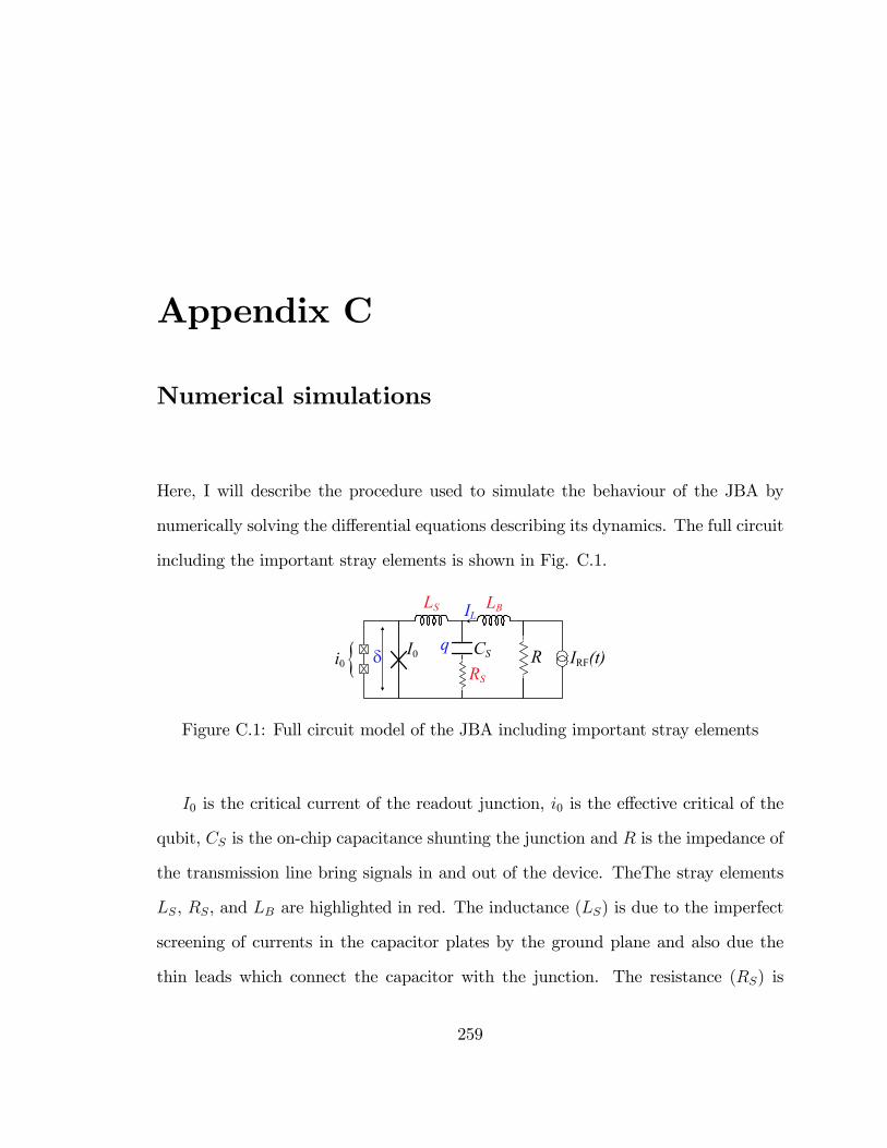
Appendix C
Numerical simulations
Here, I will describe the procedure used to simulate the behaviour of the JBA by
numerically solving the di¤erential equations describing its dynamics. The full circuit
including the important stray elements is shown in Fig. C.1.
Figure C.1: Full circuit model of the JBA including important stray elements
I0 is the critical current of the readout junction, i0 is the e¤ective critical of the
qubit, CS is the on-chip capacitance shunting the junction and R is the impedance of
the transmission line bring signals in and out of the device. TheThe stray elements
LS, RS, and LB are highlighted in red. The inductance (LS) is due to the imperfect
screening of currents in the capacitor plates by the ground plane and also due the
thin leads which connect the capacitor with the junction. The resistance (RS) is
259
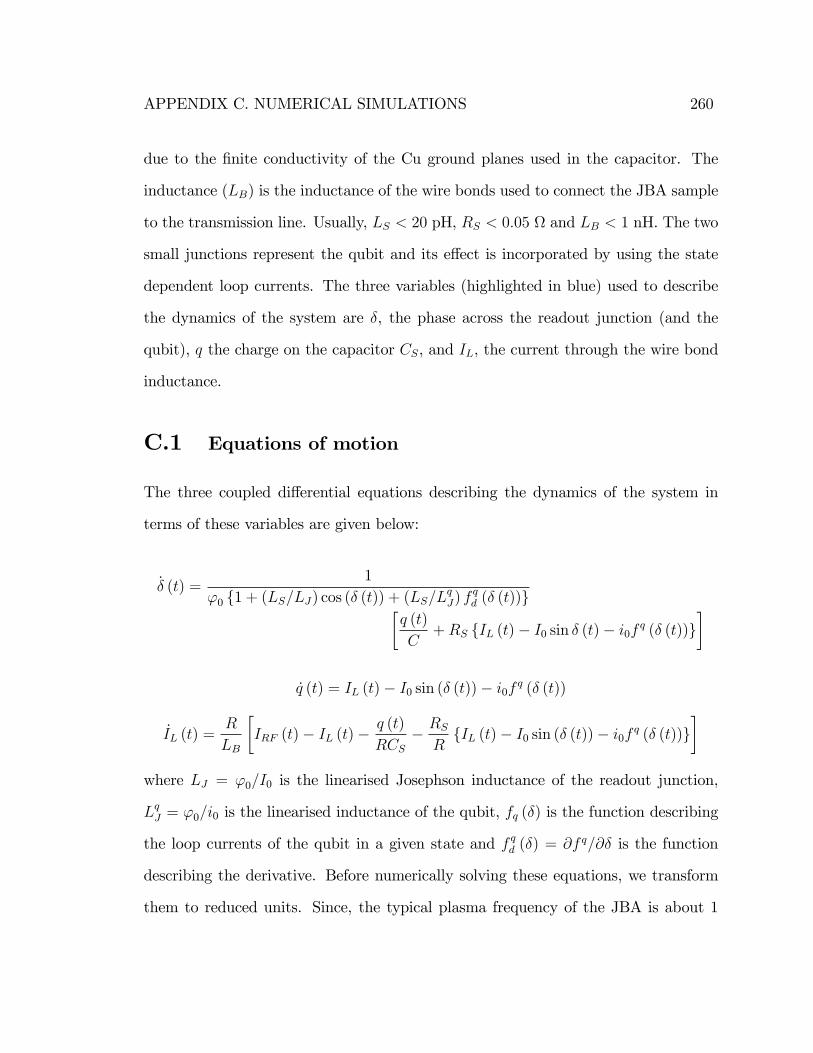
APPENDIX C. NUMERICAL SIMULATIONS 260
due to the �nite conductivity of the Cu ground planes used in the capacitor. The
inductance (LB) is the inductance of the wire bonds used to connect the JBA sample
to the transmission line. Usually, LS < 20 pH, RS < 0:05 and LB < 1 nH. The two
small junctions represent the qubit and its e¤ect is incorporated by using the state
dependent loop currents. The three variables (highlighted in blue) used to describe
the dynamics of the system are �, the phase across the readout junction (and the
qubit), q the charge on the capacitor CS, and IL, the current through the wire bond
inductance.
C.1 Equations of motion
The three coupled di¤erential equations describing the dynamics of the system in
terms of these variables are given below:
_� (t) =1
'0 f1 + (LS=LJ) cos (� (t)) + (LS=LqJ) f
qd (� (t))g�
q (t)
C+RS fIL (t)� I0 sin � (t)� i0f q (� (t))g
�
_q (t) = IL (t)� I0 sin (� (t))� i0f q (� (t))
_IL (t) =R
LB
�IRF (t)� IL (t)�
q (t)
RCS� RSRfIL (t)� I0 sin (� (t))� i0f q (� (t))g
�where LJ = '0=I0 is the linearised Josephson inductance of the readout junction,
LqJ = '0=i0 is the linearised inductance of the qubit, fq (�) is the function describing
the loop currents of the qubit in a given state and f qd (�) = @f q=@� is the function
describing the derivative. Before numerically solving these equations, we transform
them to reduced units. Since, the typical plasma frequency of the JBA is about 1
APPENDIX C. NUMERICAL SIMULATIONS 261
GHz and the critical current of the junction is about 1 �A, we change into a system
of units where time is measured in ns, current in �A. So we make the following
transformations
t = 109�
� (t) = 2�x (�)
q (t) = RCs 10�6y (�)
IL (t) = 10�6z (t)
In these new system of variables x (�), y (�) and z (�), the equations become
_x (�) =Q
f1 + (LS=LJ) cos (2�x (�)) + (LS=LqJ) fqd (2�x (�))g�
fJGHzI0�A
��y (�) +
RSRfz (�)� I0�A sin 2�x (t)� i0�Af q (2�x (�))g
�
_y (�) =2�
QfJGHz [z (�)� I0�A sin (2�x (�))� i0�Af q (2�x (�))]
_IL (t) =2�
QfJGHz
�LJLB
��IRF�A (�)� z (�)� y (�)�
RSRfz (�)� I0�A sin 2�x (t)� i0�Af q (2�x (�))g
�
The reduced equations are solved using 4th order Runge-Kutta method [107]. The
code is written in C++ and the compiled code is imported into the Labview software
which o¤ers many data processing routines and easy to use graphical interface. The
drive and the noise current are generated in Labview. The noise signal is generated
APPENDIX C. NUMERICAL SIMULATIONS 262
by using a Gaussian distributed random number generator in Labview. In order to
correctly mimic thermal noise current at temperature T and resistance R, the random
number generator is set to zero mean and a standard deviation Irmsgiven [60]by
Irms =
r2kBT
R�t
where �t is the time step used in the numerical simulation. In reduced units de�ned
above this becomes
irms�A =
r2kBT
R��1023
where irms�A is the standard deviation of the current noise distribution.
The loop current functions f q and f qd are computed in Mathematica and passed
on to the C++ code as an array of 1000 values de�ned for a range of � going from 0
to �. The code uses linear interpolation compute the functions from these array of
values.
Bibliography
[1] M. Muck, C. Welzel, and J. Clarke, Superconducting quantum interferencedevice ampli�ers at gigahertz frequencies, Appl. Phys. Lett. 82(19), 3266�3268(2003).
[2] R. J. Schoelkopf, P. Wahlgren, A. A. Kozhevnikov, P. Delsing, and D. E. Prober,The radio-frequency single-electron transistor (RF-SET): A fast and ultrasen-sitive electrometer, Science 280(5367), 1238�1242 (1998).
[3] B. D. Josephson, Coupled Superconductors, Rev. Mod. Phys. 36(1P1), 216(1964).
[4] Y. Nakamura, Y. A. Pashkin, and J. S. Tsai, Coherent control of macroscopicquantum states in a single-Cooper-pair box, Nature 398(6730), 786�788 (1999).
[5] J. E. Mooij, T. P. Orlando, L. Levitov, L. Tian, C. H. van der Wal, and S. Lloyd,Josephson persistent-current qubit, Science 285(5430), 1036�1039 (1999).
[6] D. Vion, A. Aassime, A. Cottet, P. Joyez, H. Pothier, C. Urbina, D. Esteve,and M. H. Devoret, Manipulating the quantum state of an electrical circuit,Science 296(5569), 886�889 (2002).
[7] J. M. Martinis, S. Nam, J. Aumentado, and C. Urbina, Rabi oscillations in alarge Josephson-junction qubit, Phys. Rev. Lett. 89(11), 117901 (2002).
[8] E. Abraham and S. D. Smith, Optical bistability and related devices, Reportson Progress in Physics 45(8), 815�885 (1982).
[9] B. Yurke, L. R. Corruccini, P. G. Kaminsky, L. W. Rupp, A. D. Smith, A. H.Silver, R. W. Simon, and E. A. Whittaker, Observation of Parametric Ampli-�cation and Deampli�cation in a Josephson Parametric-Ampli�er, Phys. Rev.A 39(5), 2519�2533 (1989).
[10] C. M. Caves, Quantum Limits on Noise in Linear-Ampli�ers, Phys. Rev. D26(8), 1817�1839 (1982).
263

BIBLIOGRAPHY 264
[11] R. Bradley, J. Clarke, D. Kinion, L. J. Rosenberg, K. van Bibber, S. Matsuki,M. Muck, and P. Sikivie, Microwave cavity searches for dark-matter axions,Rev. Mod. Phys. 75(3), 777�817 (2003).
[12] N. Wadefalk, A. Mellberg, I. Angelov, M. E. Barsky, S. Bui, E. Choumas, R. W.Grundbacher, E. L. Kollberg, R. Lai, N. Rorsman, P. Starski, J. Stenarson,D. C. Streit, and H. Zirath, Cryogenic wide-band ultra-low-noise IF ampli�ersoperating at ultra-low DC power, IEEE Transactions on Microwave Theory andTechniques 51(6), 1705�1711 (2003).
[13] P. F. Michelson, J. C. Price, and R. C. Taber, Resonant-Mass Detectors ofGravitational-Radiation, Science 237(4811), 150�157 (1987).
[14] K. Schwab, Spring constant and damping constant tuning of nanomechanicalresonators using a single-electron transistor, Appl. Phys. Lett. 80(7), 1276�1278(2002).
[15] M. Muck, J. B. Kycia, and J. Clarke, Superconducting quantum interferencedevice as a near-quantum-limited ampli�er at 0.5 GHz, Appl. Phys. Lett. 78(7),967�969 (2001).
[16] M. H. Devoret and R. J. Schoelkopf, Amplifying quantum signals with thesingle-electron transistor, Nature 406(6799), 1039�1046 (2000).
[17] H. A. Haus and J. A. Mullen, Quantum Noise in Linear Ampli�ers, PhysicalReview 128(5), 2407 (1962).
[18] C. M. Caves, K. S. Thorne, R. W. P. Drever, V. D. Sandberg, and M. Zimmer-mann, On the Measurement of a Weak Classical Force Coupled to a Quantum-Mechanical Oscillator .1. Issues of Principle, Rev. Mod. Phys. 52(2), 341�392(1980).
[19] J. M. Courty, F. Grassia, and S. Reynaud, Quantum noise in ideal operationalampli�ers, Europhysics Letters 46(1), 31�37 (1999).
[20] J.-M. Courty, F. Grassia, and S. Reynaud, Thermal and quantum noise inactive systems, arXiv:quant-ph/0110021v1 (2000).
[21] K. Wiesenfeld and B. McNamara, Period-doubling systems as small-signal am-pli�ers, Phys. Rev. Lett. 55(1), 13�16 (1985).
[22] K. Wiesenfeld and B. McNamara, Small-signal ampli�cation in bifurcatingdynamical systems, Phys. Rev. A 33(1), 629�642 (1986).
BIBLIOGRAPHY 265
[23] V. M. Eguíluz, M. Ospeck, Y. Choe, A. J. Hudspeth, and M. O. Magnasco,Essential Nonlinearities in Hearing, Phys. Rev. Lett. 84(22), 5232�5235 (2000).
[24] S. Martignoli, J.-J. van der Vyver, A. Kern, Y. Uwate, and R. Stoop, Analogelectronic cochlea with mammalian hearing characteristics, Appl. Phys. Lett.91(6), 064108 (2007).
[25] R. Movshovich, B. Yurke, P. G. Kaminsky, A. D. Smith, A. H. Silver, R. W.Simon, and M. V. Schneider, Observation of zero-point noise squeezing via aJosephson-parametric ampli�er, Phys. Rev. Lett. 65(12), 1419�1422 (1990).
[26] P. H. Bryant, R. Movshovich, and B. Yurke, Noise rise in nondegenerate para-metric ampli�ers, Phys. Rev. Lett. 66(20), 2641�2644 (1991).
[27] M. I. Dykman and M. A. Krivoglaz, Fluctuations in Non-Linear Systems NearBifurcations Corresponding to the Appearance of New Stable States, PhysicaA 104(3), 480�494 (1980).
[28] I. Siddiqi, R. Vijay, F. Pierre, C. M. Wilson, L. Frunzio, M. Metcalfe, C. Rigetti,R. J. Schoelkopf, M. H. Devoret, D. Vion, and D. Esteve, Direct observationof dynamical bifurcation between two driven oscillation states of a Josephsonjunction, Phys. Rev. Lett. 94(2), 027005 (2005).
[29] I. Siddiqi, R. Vijay, M. Metcalfe, E. Boaknin, L. Frunzio, R. J. Schoelkopf, andM. H. Devoret, Dispersive measurements of superconducting qubit coherencewith a fast latching readout, Phys. Rev. B 73(5), 054510 (2006).
[30] M. H. Devoret, A. Wallra¤, and J. M. Martinis, Superconducting Qubits: AShort Review, 2004.
[31] C. Monroe, D. M. Meekhof, B. E. King, W. M. Itano, and D. J. Wineland,Demonstration of a Fundamental Quantum Logic Gate, Phys. Rev. Lett.75(25), 4714�4717 (1995).
[32] J. J. García-Ripoll, P. Zoller, and J. I. Cirac, Speed Optimized Two-Qubit Gateswith Laser Coherent Control Techniques for Ion Trap Quantum Computing,Phys. Rev. Lett. 91(15), 157901 (2003).
[33] A. Wallra¤, D. I. Schuster, A. Blais, L. Frunzio, R. S. Huang, J. Majer, S. Ku-mar, S. M. Girvin, and R. J. Schoelkopf, Strong coupling of a single photonto a superconducting qubit using circuit quantum electrodynamics, Nature431(7005), 162�167 (2004).
BIBLIOGRAPHY 266
[34] I. Chiorescu, P. Bertet, K. Semba, Y. Nakamura, C. J. P. M. Harmans, andJ. E. Mooij, Coherent dynamics of a �ux qubit coupled to a harmonic oscillator,Nature 431(7005), 159�162 (2004).
[35] M. Tinkham, Introduction to Superconductivity, Dover, 2004.
[36] M. Büttiker, Zero-current persistent potential drop across small-capacitanceJosephson junctions, Phys. Rev. B 36(7), 3548�3555 (1987).
[37] V. Bouchiat, D. Vion, P. Joyez, D. Esteve, and M. H. Devoret, Quantumcoherence with a single Cooper pair, Physica Scripta T76, 165�170 (1998).
[38] A. Cottet, Implementation of a quantum bit in a superconducting circuit, PhDthesis, l�Universite Paris VI, 2002.
[39] J. Mannik and J. E. Lukens, E¤ect of measurement on the periodicity of theCoulomb staircase of a superconducting box, Phys. Rev. Lett. 92(5), 057004(2004).
[40] G. Ithier, E. Collin, P. Joyez, P. J. Meeson, D. Vion, D. Esteve, F. Chiarello,A. Shnirman, Y. Makhlin, J. Schrie�, and G. Schon, Decoherence in a super-conducting quantum bit circuit, Phys. Rev. B 72(13), 134519 (2005).
[41] J. Mygind, N. F. Pedersen, and O. H. Soerensen, Direct Detection of Para-metrically Generated Half-Harmonic Voltage in a Josephson Tunnel Junction,Appl. Phys. Lett. 29(5), 317�319 (1976).
[42] T. Holst and J. B. Hansen, The Plasma Resonance in Microwave-Driven SmallJosephson Tunnel-Junctions, Physica B 165, 1649�1650 (1990).
[43] M. Metcalfe, E. Boaknin, V. Manucharyan, R. Vijay, I. Siddiqi, C. Rigetti,L. Frunzio, R. J. Schoelkopf, and M. H. Devoret, Measuring the decoherenceof a quantronium qubit with the cavity bifurcation ampli�er, Phys. Rev. B76(17), 174516 (2007).
[44] J. Koch, T. M. Yu, J. Gambetta, A. A. Houck, D. I. Schuster, J. Majer, A. Blais,M. H. Devoret, S. M. Girvin, and R. J. Schoelkopf, Charge-insensitive qubitdesign derived from the Cooper pair box, Phys. Rev. A 76(4), 042319 (2007).
[45] J. Majer, J. M. Chow, J. M. Gambetta, J. Koch, B. R. Johnson, J. A. Schreier,L. Frunzio, D. I. Schuster, A. A. Houck, A. Wallra¤, A. Blais, M. H. Devoret,S. M. Girvin, and R. J. Schoelkopf, Coupling superconducting qubits via acavity bus, Nature 449(7161), 443�447 (2007).

BIBLIOGRAPHY 267
[46] R. W. Simmonds, K. M. Lang, D. A. Hite, S. Nam, D. P. Pappas, and J. M.Martinis, Decoherence in Josephson phase qubits from Junction resonators,Phys. Rev. Lett. 93(7), 077003 (2004).
[47] D. I. Schuster, A. Wallra¤, A. Blais, L. Frunzio, R. S. Huang, J. Majer, S. M.Girvin, and R. J. Schoelkopf, AC-Stark shift and dephasing of a superconduct-ing qubit strongly coupled to a cavity �eld, Phys. Rev. Lett. 94(12), 123602(2005).
[48] J. M. Martinis, M. H. Devoret, and J. Clarke, Experimental tests for thequantum behavior of a macroscopic degree of freedom: The phase di¤erenceacross a Josephson junction, Phys. Rev. B 35(10), 4682�4698 (1987).
[49] M. I. Dykman and V. N. Smelyansky, Quantum-Theory of Transitions betweenStable States of a Nonlinear Oscillator Interacting with the Medium in a Res-onant Field, Zhurnal Eksperimentalnoi i Teoreticheskoi Fiziki 94(9), 61�74(1988).
[50] M. Marthaler and M. I. Dykman, Switching via quantum activation: A para-metrically modulated oscillator, Phys. Rev. A 73(4), 042108 (2006).
[51] M. I. Dykman, Critical exponents in metastable decay via quantum activation,Phys. Rev. E 75(1), 011101 (2007).
[52] I. Katz, A. Retzker, R. Straub, and R. Lifshitz, Signatures for a Classical toQuantum Transition of a Driven Nonlinear Nanomechanical Resonator, Phys.Rev. Lett. 99(4), 040404 (2007).
[53] G. T. Moore, Quantum Theory of Electromagnetic Field in a Variable-LengthOne-Dimensional Cavity, Journal of Mathematical Physics 11(9), 2679 (1970).
[54] V. V. Dodonov, Dynamical Casimir e¤ect in a nondegenerate cavity with lossesand detuning, Phys. Rev. A 58(5), 4147�4152 (1998).
[55] A. Lambrecht, M. T. Jaekel, and S. Reynaud, Motion induced radiation froma vibrating cavity, Phys. Rev. Lett. 77(4), 615�618 (1996).
[56] R. Vijay, I. Siddiqi, P. Hya�l, M.Metcalfe, L. Frunzio, and M. H. Devoret, Inpreparation.
[57] I. Siddiqi, R. Vijay, F. Pierre, C. M. Wilson, M. Metcalfe, C. Rigetti, L. Frunzio,and M. H. Devoret, RF-driven Josephson bifurcation ampli�er for quantummeasurement, Phys. Rev. Lett. 93(20), 207002 (2004).

BIBLIOGRAPHY 268
[58] L. D. Landau and E. M. Lifshitz, Small Oscillations, chapter V, Mechanics,Pergamon Press, 1960.
[59] V. E. Manucharyan, E. Boaknin, M. Metcalfe, R. Vijay, I. Siddiqi, and M. De-voret, Microwave bifurcation of a Josephson junction: Embedding-circuit re-quirements, Phys. Rev. B 76(1), 014524 (2007).
[60] R. L. Kautz, Thermally Induced Escape - the Principle of Minimum AvailableNoise Energy, Phys. Rev. A 38(4), 2066�2080 (1988).
[61] M. I. Dykman and M. A. Krivoglaz, Theory of Fluctuational Transitions be-tween the Stable States of a Non-Linear Oscillator, Zhurnal Eksperimentalnoii Teoreticheskoi Fiziki 77(1), 60�73 (1979).
[62] M. I. Dykman and V. N. Smelyanski, Fluctuational Transitions between StableStates of a Nonlinear Oscillator Driven by Random Resonant Force, Phys. Rev.A 41(6), 3090�3102 (1990).
[63] H. A. Kramers, Brownian motion in a �eld of force and the di¤usion model ofchemical reactions, Physica 7, 284�304 (1940).
[64] P. Hänggi, P. Talkner, and M. Borkovec, Reaction-rate theory: �fty years afterKramers, Rev. Mod. Phys. 62(2), 251�341 (1990).
[65] M. H. Devoret, D. Esteve, J. M. Martinis, A. Cleland, and J. Clarke, Reso-nant Activation of a Brownian Particle Out of a Potential Well - Microwave-Enhanced Escape from the Zero-Voltage State of a Josephson Junction, Phys.Rev. B 36(1), 58�73 (1987).
[66] M. Metcalfe, A new microwave resonator readout scheme for superconductingqubits, PhD thesis, Yale University, 2008.
[67] J. Clarke, Principles and Applications of Squids, Proceedings of the IEEE77(8), 1208�1223 (1989).
[68] I. Chiorescu, Y. Nakamura, C. J. P. M. Harmans, and J. E. Mooij, Coherentquantum dynamics of a superconducting �ux qubit, Science 299(5614), 1869�1871 (2003).
[69] V. Bouchiat, Quantum �uctuations of the charge in single electron and singleCooper pair devices, PhD thesis, l�Universite Paris VI, 1997.
[70] F. L. Claude Cohen-Tannoudji, Bernard Diu, Quantum Mechanics, John Wileyand Sons, Hermann, 1977.
BIBLIOGRAPHY 269
[71] Abragam, The principles of nuclear magnetism, Oxford University Press, 1961.
[72] I. I. Rabi, Space Quantization in a Gyrating Magnetic Field, Phys. Rev. 51(8),652�654 (1937).
[73] N. F. Ramsey, AMolecular BeamResonance Method with Separated OscillatingFields, Phys. Rev. 78(6), 695�699 (1950).
[74] K. W. Lehnert, K. Bladh, L. F. Spietz, D. Gunnarsson, D. I. Schuster, P. Dels-ing, and R. J. Schoelkopf, Measurement of the Excited-State Lifetime of aMicroelectronic Circuit, Phys. Rev. Lett. 90(2), 027002 (2003).
[75] E. Il�ichev, N. Oukhanski, A. Izmalkov, T. Wagner, M. Grajcar, H. G. Meyer,A. Y. Smirnov, A. M. van den Brink, M. H. S. Amin, and A. M. Zagoskin,Continuous monitoring of Rabi oscillations in a Josephson �ux qubit, Phys.Rev. Lett. 91(9), 097906 (2003).
[76] M. Grajcar, A. Izmalkov, E. Il�ichev, T. Wagner, N. Oukhanski, U. Hubner,T. May, I. Zhilyaev, H. E. Hoenig, Y. S. Greenberg, V. I. Shnyrkov, D. Born,W. Krech, H.-G. Meyer, A. M. van den Brink, and M. H. S. Amin, Low-frequency measurement of the tunneling amplitude in a �ux qubit, Phys. Rev.B 69(6), 060501 (2004).
[77] A. Lupascu, C. J. M. Verwijs, R. N. Schouten, C. J. P. M. Harmans, and J. E.Mooij, Nondestructive readout for a superconducting �ux qubit, Phys. Rev.Lett. 93(17), 177006 (2004).
[78] C. M. Wilson, T. Duty, F. Persson, M. Sandberg, G. Johansson, and P. Delsing,Coherence Times of Dressed States of a Superconducting Qubit under ExtremeDriving, Phys. Rev. Lett. 98(25), 257003 (2007).
[79] N. Boulant, G. Ithier, P. Meeson, F. Nguyen, D. Vion, D. Esteve, I. Siddiqi,R. Vijay, C. Rigetti, F. Pierre, and M. Devoret, Quantum nondemolition read-out using a Josephson bifurcation ampli�er, Phys. Rev. B 76(1), 014525 (2007).
[80] D. Vion, A. Aassime, A. Cottet, P. Joyez, H. Pothier, C. Urbina, D. Esteve,and M. H. Devoret, Rabi oscillations, Ramsey fringes and spin echoes in anelectrical circuit, Fortschritte Der Physik-Progress of Physics 51(4-5), 462�468(2003).
[81] P. Bertet, I. Chiorescu, G. Burkard, K. Semba, C. J. P. M. Harmans, D. P.DiVincenzo, and J. E. Mooij, Dephasing of a superconducting qubit inducedby photon noise, Phys. Rev. Lett. 95(25), 257002 (2005).

BIBLIOGRAPHY 270
[82] P. Bertet, I. Chiorescu, K. Semba, C. J. P. M. Harmans, and J. E. Mooij,Detection of a persistent-current qubit by resonant activation, Phys. Rev. B70(1), 100501 (2004).
[83] V. B. Braginsky and F. Y. Khalili, Quantum nondemolition measurements: theroute from toys to tools, Rev. Mod. Phys. 68(1), 1�11 (1996).
[84] V. B. Braginsky, Y. I. Vorontsov, and K. S. Thorne, Quantum NondemolitionMeasurements, Science 209, 547�557 (1980).
[85] A. B. Zorin, F.-J. Ahlers, J. Niemeyer, T. Weimann, H. Wolf, V. A. Krupenin,and S. V. Lotkhov, Background charge noise in metallic single-electron tunnel-ing devices, Phys. Rev. B 53(20), 13682�13687 (1996).
[86] J. A. Schreier, A. A. Houck, J. Koch, D. I. Schuster, B. R. Johnson, J. M.Chow, J. M. Gambetta, J. Majer, L. Frunzio, M. H. Devoret, S. M. Girvin, andR. J. Schoelkopf, Suppressing Charge Noise Decoherence in SuperconductingCharge Qubits, 2007.
[87] M. Boissonneault, J. Gambetta, and A. Blais, In preparation, (2008).
[88] M. Ste¤en, M. Ansmann, R. C. Bialczak, N. Katz, E. Lucero, R. McDermott,M. Neeley, E. M. Weig, A. N. Cleland, and J. M. Martinis, Measurement of theEntanglement of Two Superconducting Qubits via State Tomography, Science313(5792), 1423�1425 (2006).
[89] N. Katz, M. Ansmann, R. C. Bialczak, E. Lucero, R. McDermott, M. Neeley,M. Ste¤en, E. M. Weig, A. N. Cleland, J. M. Martinis, and A. N. Korotkov,Coherent State Evolution in a Superconducting Qubit from Partial-CollapseMeasurement, Science 312(5779), 1498�1500 (2006).
[90] M. Ste¤en, M. Ansmann, R. McDermott, N. Katz, R. C. Bialczak, E. Lucero,M. Neeley, E. M. Weig, A. N. Cleland, and J. M. Martinis, State Tomography ofCapacitively Shunted Phase Qubits with High Fidelity, Phys. Rev. Lett. 97(5),050502 (2006).
[91] A. Lupascu, E. F. C. Driessen, L. Roschier, C. J. P. M. Harmans, and J. E.Mooij, High-contrast dispersive readout of a superconducting �ux qubit usinga nonlinear resonator, Phys. Rev. Lett. 96(12), 127003 (2006).
[92] A. Wallra¤, D. I. Schuster, A. Blais, L. Frunzio, J. Majer, M. H. Devoret,S. M. Girvin, and R. J. Schoelkopf, Approaching unit visibility for control of asuperconducting qubit with dispersive readout, Phys. Rev. Lett. 95(6), 060501(2005).
BIBLIOGRAPHY 271
[93] R. J. Schoelkopf, Private communication.
[94] C. Rigetti, Private communication.
[95] A. O. Caldeira and A. J. Leggett, Quantum tunnelling in a dissipative system,Annals of Physics 149(2), 374�456 (1983).
[96] B. Yurke, Input-Output theory, chapter 3, page 53, Quantum Squeezing,Springer, 2004.
[97] T. A. Fulton and L. N. Dunkleberger, Lifetime of the zero-voltage state inJosephson tunnel junctions, Phys. Rev. B 9(11), 4760�4768 (1974).
[98] G. Milburn and D. F. Walls, Production of squeezed states in a degenerateparametric ampli�er, Optics Communications, 39(6), 401�404 (1981).
[99] B. Yurke, Use of cavities in squeezed-state generation, Phys. Rev. A 29(1),408�410 (1984).
[100] I. Serban and F. K. Wilhelm, Dynamical tunneling in macroscopic systems,arXiv.org:0706.3022 (2007).
[101] B. Yurke and E. Buks, Performance of Cavity-Parametric Ampli�ers, Em-ploying Kerr Nonlinearites, in the Presence of Two-Photon Loss, Journal ofLightwave Technology 24(12), 5054�5066 (2006).
[102] V. V. Dodonov and A. V. Dodonov, Quantum harmonic oscillator and non-stationary Casimir e¤ect, Journal of Russian Laser Research 26(6), 445�483(2005).
[103] W. G. Unruh, Notes on Black-Hole Evaporation, Phys. Rev. D 14(4), 870�892(1976).
[104] E. Segev, B. Abdo, O. Shtempluck, E. Buks, and B. Yurke, Prospects of em-ploying superconducting stripline resonators for studying the dynamical Casimire¤ect experimentally, Physics Letters A, 370(3-4), 202�206 (2007).
[105] B. Yurke, P. G. Kaminsky, R. E. Miller, E. A. Whittaker, A. D. Smith, A. H.Silver, and R. W. Simon, Observation of 4.2-K equilibrium-noise squeezing viaa Josephson-parametric ampli�er, Phys. Rev. Lett. 60(9), 764�767 (1988).
[106] N. Bergeal, R. Vijay, V. Manucharyan, I. Siddiqi, R. J. Schoelkopf, S. M. Girvin,and M. H. Devoret, In preparation, (2008).
BIBLIOGRAPHY 272
[107] H. Press, S. Teukolsky, W. Vetterling, and B. Flannery, Numerical Recipes inC++. The Art of Scienti�c Computing, second edition, Cambridge UniversityPress, 2002.
![arXiv:1503.04364v1 [cond-mat.supr-con] 15 Mar 2015 · (Dated: March 17, 2015) Josephson parametric ampli ers have become a critical tool in superconducting device physics due to their](https://img.pdfslide.us/doc/110x75/5f63af5a5896ec767a21b68f/arxiv150304364v1-cond-matsupr-con-15-mar-2015-dated-march-17-2015-josephson.jpg)