Embed Size (px)
Citation preview
ABSTRACT
Title of Document: DESIGN OF A WIRELESS FISH LENGTH
MEASURING BOARD FOR FISHERIES RESEARCH
Omar Farooq Amin, Master of Science, 2006 Directed By: Associate Professor, Omar Ramahi, Department
of Electrical and Computer Engineering, University of Waterloo.
The goal of this work is to design and implement the fundamental technology needed
to construct a wireless fish measuring board that performs non-contact length
measurements. After taking the measurement, the board sends the information
containing the length of the fish amongst other parameters wirelessly to a receiver
located several meters away. The receiver in turn decodes the information and sends
it for display on a computer monitor. The wireless transmission must be immune to
the typical non-line of sight (NLOS) environments that are found in the fisheries
industry. The non-contact technique used here is based on the Hall-effect sensing
mechanism. The wireless link operates in the 902-928MHz Industrial, Scientific and
Medical (ISM) band. The entire system was fully developed using Commercial Off-
the-Shelf (COTS) components and is shown to perform satisfactorily in typical NLOS
environment.
DESIGN OF A WIRELESS FISH LENGTH MEASURING BOARD FOR FISHERIES RESEARCH
By
Omar Farooq Amin
Thesis submitted to the Faculty of the Graduate School of the University of Maryland, College Park, in partial fulfillment
of the requirements for the degree of Master of Science
2006 Advisory Committee: Professor Omar Ramahi, Chair Professor Bruce Jacob Professor Victor Granatstein

© Copyright by Omar Farooq Amin
2006

ii
DEDICATION
To my family.

iii
ACKNOWLEDGEMENTS
Thanks to Professor Ramahi for all his help and the family for all the support.
iv
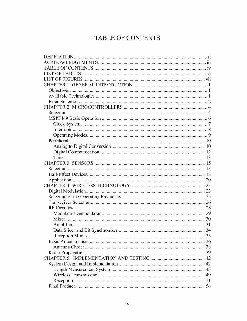
TABLE OF CONTENTS DEDICATION.............................................................................................................. ii ACKNOWLEDGEMENTS......................................................................................... iii TABLE OF CONTENTS............................................................................................. iv LIST OF TABLES....................................................................................................... vi LIST OF FIGURES .................................................................................................... vii CHAPTER 1: GENERAL INTRODUCTION ............................................................. 1
Objectives ................................................................................................................. 1 Available Technologies ............................................................................................ 1 Basic Scheme ............................................................................................................ 2
CHAPTER 2: MICROCONTROLLERS ..................................................................... 4 Selection.................................................................................................................... 4 MSPF449 Basic Operation ....................................................................................... 6
Clock System ........................................................................................................ 7 Interrupts ............................................................................................................... 8 Operating Modes................................................................................................... 9
Peripherals............................................................................................................... 10 Analog to Digital Conversion ............................................................................. 10 Digital Communication....................................................................................... 12 Timer................................................................................................................... 13
CHAPTER 3: SENSORS............................................................................................ 15 Selection.................................................................................................................. 15 Hall-Effect Devices................................................................................................. 18 Application.............................................................................................................. 20
CHAPTER 4: WIRELESS TECHNOLOGY ............................................................. 23 Digital Modulation.................................................................................................. 23 Selection of the Operating Frequency..................................................................... 25 Transceiver Selection.............................................................................................. 26 RF Circuitry ............................................................................................................ 28
Modulator/Demodulator ..................................................................................... 29 Mixer................................................................................................................... 30 Amplifiers ........................................................................................................... 31 Data Slicer and Bit Synchronizer........................................................................ 34 Reception Modes ................................................................................................ 35
Basic Antenna Facts................................................................................................ 36 Antenna Choice................................................................................................... 38
Radio Propagation................................................................................................... 39 CHAPTER 5: IMPLEMENTATION AND TESTING ............................................. 42
System Design and Implementation ....................................................................... 42 Length Measurement System.............................................................................. 43 Wireless Transmission ........................................................................................ 49 Reception ............................................................................................................ 51
Final Product........................................................................................................... 54
v
Device Testing ........................................................................................................ 56 Testing Results.................................................................................................... 57 Majority Vote Analysis....................................................................................... 60
CHAPTER 6: CONCLUDING REMARKS ............................................................. 63 Future Work ............................................................................................................ 63 Conclusion .............................................................................................................. 63
APPENDIX A: LENGTH MEASUREMENT ........................................................... 65 APPENDIX B: TRANSMISION................................................................................ 94 APPENDIX C: RECEPTION................................................................................... 125 REFERENCES ......................................................................................................... 155
vi
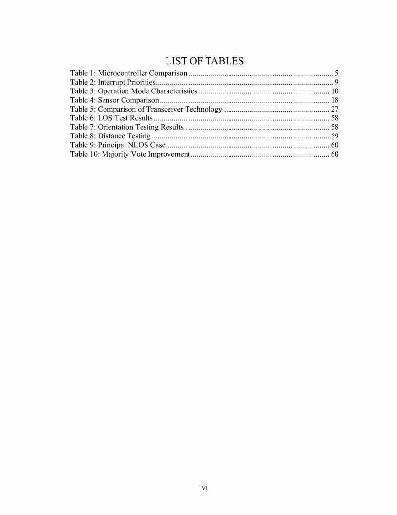
LIST OF TABLES Table 1: Microcontroller Comparison .......................................................................... 5 Table 2: Interrupt Priorities........................................................................................... 9 Table 3: Operation Mode Characteristics ................................................................... 10 Table 4: Sensor Comparison....................................................................................... 18 Table 5: Comparison of Transceiver Technology ...................................................... 27 Table 6: LOS Test Results .......................................................................................... 58 Table 7: Orientation Testing Results .......................................................................... 58 Table 8: Distance Testing ........................................................................................... 59 Table 9: Principal NLOS Case.................................................................................... 60 Table 10: Majority Vote Improvement ....................................................................... 60
vii
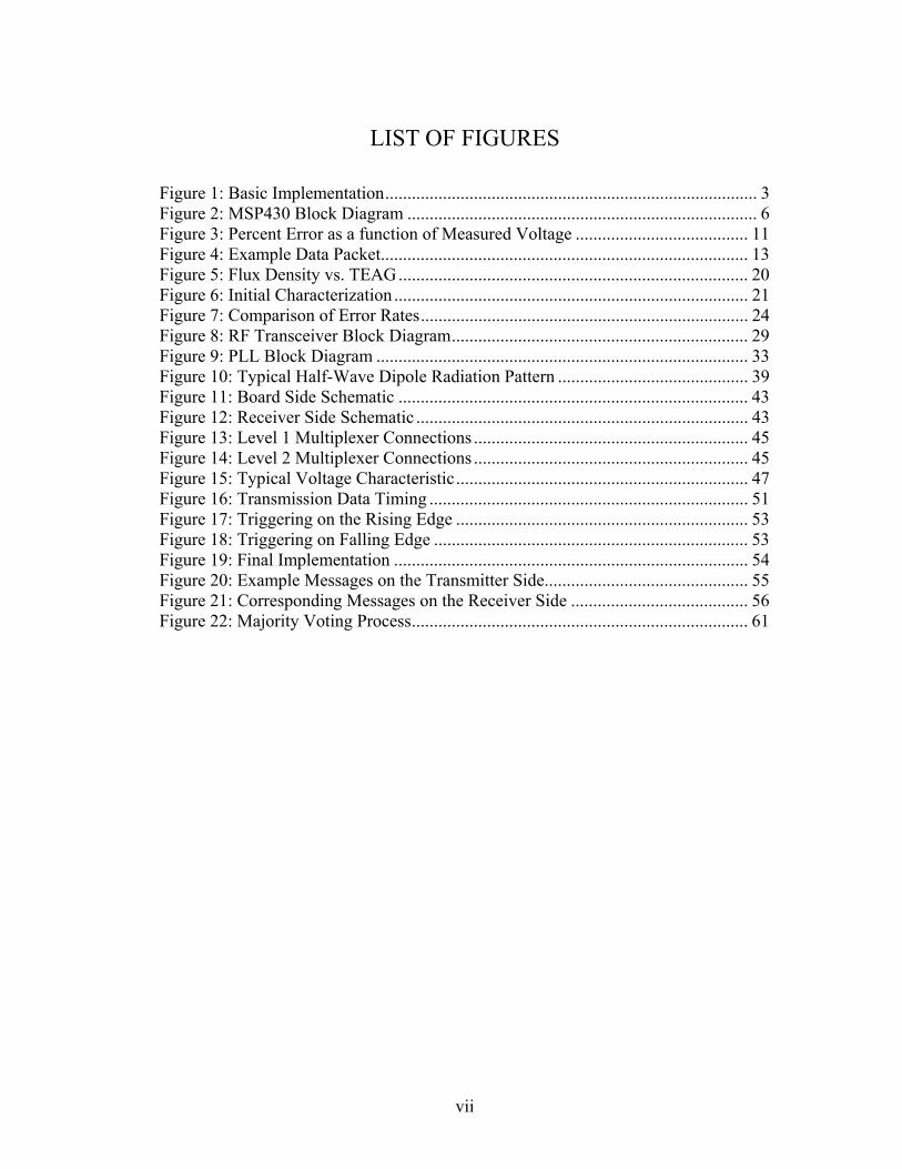
LIST OF FIGURES
Figure 1: Basic Implementation.................................................................................... 3 Figure 2: MSP430 Block Diagram ............................................................................... 6 Figure 3: Percent Error as a function of Measured Voltage ....................................... 11 Figure 4: Example Data Packet................................................................................... 13 Figure 5: Flux Density vs. TEAG............................................................................... 20 Figure 6: Initial Characterization ................................................................................ 21 Figure 7: Comparison of Error Rates.......................................................................... 24 Figure 8: RF Transceiver Block Diagram................................................................... 29 Figure 9: PLL Block Diagram .................................................................................... 33 Figure 10: Typical Half-Wave Dipole Radiation Pattern ........................................... 39 Figure 11: Board Side Schematic ............................................................................... 43 Figure 12: Receiver Side Schematic ........................................................................... 43 Figure 13: Level 1 Multiplexer Connections .............................................................. 45 Figure 14: Level 2 Multiplexer Connections .............................................................. 45 Figure 15: Typical Voltage Characteristic.................................................................. 47 Figure 16: Transmission Data Timing ........................................................................ 51 Figure 17: Triggering on the Rising Edge .................................................................. 53 Figure 18: Triggering on Falling Edge ....................................................................... 53 Figure 19: Final Implementation ................................................................................ 54 Figure 20: Example Messages on the Transmitter Side.............................................. 55 Figure 21: Corresponding Messages on the Receiver Side ........................................ 56 Figure 22: Majority Voting Process............................................................................ 61

1
CHAPTER 1: GENERAL INTRODUCTION
Objectives
The goal of this project is to design the primary technology needed to construct a board
that allows a user to perform length measurements on an object accurate to 1mm and send that
information wirelessly to a receiver. The board will be used in fisheries research to measure the
length of fish for various environmental reasons. Since the creatures being measured often move
around unpredictably, we strive to design a device that has no moving parts and no wires
associated with it that the creatures could become entangled in or break. Moreover, since the
board will be subject to a diverse set of weather and other environmental conditions, the actual
sensing elements cannot be left exposed. Thus the position sensing then must be non-contact.
In addition to these basic functional goals, we also design the board out of Commercially
Off-the-Shelf (COTS) available products so that it can be produced in greater volumes at a later
time without the need for custom electronics. Another consequence of this mass production is that
the individual elements that make up the board should be as cost effective as possible. We also, of
course, take all steps to ensure that the use of the board is as simple as possible so as to remove
human error from the measurement.
As far as the wireless connection is concerned, the most important feature is that it be
able to perform without line-of-sight. We design the device for short range operation in which the
receiver is located a few feet from the transmitter with various non-metallic barriers obstructing
the line of sight.
Available Technologies
There is a wide array of fish length measuring technologies available in the fisheries
industry. The main manufactures of these boards are Wildco, Limnoterra, Scantrol and Juniper
2
Systems. The first of these companies, Wildco, manufactures the 118-B30 fish measuring board
(FMB). This FMB simply consists of a flat surface and a moving brass indicator arm that is
placed at the end of the fish. Instead of taking an electrical measurement, this device simply
allows for the end of the object to be marked and the measurement read off a number tape [1].
The next manufacturer is Limnoterra which offers many variations of the FMB IV. This FMB
improves over the previous technology in that it offers electronic measurement without any
moving parts. It has 1mm accuracy as desired and also performs non-contact length measurement.
This FMB, however, does not allow for wireless transmission of the data from board to a
receiver, rather it simply displays the data on a digital screen on the board itself [2].
Similar to the device from Limnoterra, the Scantrol FM100 performs an electronic
measurement and displays it on the actual FMB, but does not wirelessly transmit the length data
to a receiver. This technology also has wires connecting the display to the FMB which can
become entangled when measuring a fish [3]. Finally, Juniper Systems manufacturers the LAT37
wFMB, which allows for electronic measurement to 1mm accuracy and wireless transmission to a
remote receiver. The main drawback of this system is that it uses a moving part to perform the
measurement [4]. Thus after surveying the available technologies we find that none fulfill our
goals.
Basic Scheme
Our basic principle in this project is to measure the length of the object using a stylus
placed at the end of the object. Sensing elements embedded in the actual board then will react to
the proximity of this stylus and produce an electrical output proportional to the proximity of the
stylus. The outputs of all the sensors will then be scanned using a series of multiplexers that
eventually report all output values to a microcontroller. This microcontroller then will determine
the length of the object and send its value to the transmitter. The transmitter will create the packet
to be sent, modulate the message and send the data to the receiver wirelessly. On the receiver

3
side, the receiver will take the transmitted packet and extract the necessary information and
display this information using a computer on the receiver side. The basic implementation of the
system is shown in Figure 1.
Figure 1: Basic Implementation

4
CHAPTER 2: MICROCONTROLLERS
Selection
The microcontrollers’ purpose is to make all decisions based on inputs from the various
sources and regulate the activity of other components. In this project, the most basic function of
the microcontroller will be to use sensor outputs to find the length of the object. After finding the
length, the microcontroller will send that data to the transmitting device which will wirelessly
send the data to the receiver.
The main criteria used to judge different microcontroller technologies are speed, cost,
power consumption, data and program memory and input/output capabilities. Since
microcontrollers are often complicated to implement, technical support and accompanying
software packages are also considerations. In accordance with our goal of designing the system
out of COTS technology, we restrict ourselves to readily available technologies.
Although speed is usually among the most important characteristics of microcontrollers,
in this project it is a secondary concern. Since many microcontrollers can deliver speeds at
fractions of one million instructions per second (MIPS) and the programs in this project do not
carry out computationally intensive operations, most microcontrollers on the market can deliver
adequate performance. Likewise, the cost of the microcontroller itself is not of paramount
importance since there will only be three microcontrollers in the entire system.
The power consumption of the microcontroller also is not of great importance since we
know beforehand that the sensors will be the main source of power usage in the system. On the
other hand, the random access memory (RAM) and program memory are important concerns in
the microcontroller selection. The microcontrollers will be responsible for holding information
from a multitude of sensors as well as holding somewhat extensive programs making the size of
the RAM and program memory important. In our case the size of the memory is more important
than the type as the speed of the memory look ups is not integral to the operation of the system.
5
The most important factor in selecting the microcontroller is its ability to take both digital
and analog inputs and send digital outputs. Since there will be multiple microcontrollers in the
entire system, they should have the ability to use both parallel and serial communication. The
metric chosen to evaluate the microcontroller’s parallel communicating ability is the number of
I/O ports as this is measure of the amount of information that can be sent at once. Next, the use of
the electrical sensors requires the microcontrollers to be able to take analog voltages
measurements. The main concern with the analog voltage measurement is the resolution of the
analog-to-digital converter (ADC) since it determines the accuracy of the measurement.
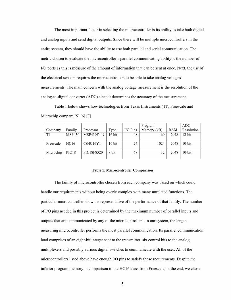
Table 1 below shows how technologies from Texas Instruments (TI), Freescale and
Microchip compare [5] [6] [7].
Company Family Processor Type I/O Pins Program Memory (kB) RAM
ADC Resolution
TI MSP430 MSP430F449 16 bit 48 60 2048 12-bit
Freescale HC16 68HC16Y1 16 bit 24 1024 2048 10-bit
Microchip PIC18 PIC18F8520 8 bit 68 32 2048 10-bit
Table 1: Microcontroller Comparison
The family of microcontroller chosen from each company was based on which could
handle our requirements without being overly complex with many unrelated functions. The
particular microcontroller shown is representative of the performance of that family. The number
of I/O pins needed in this project is determined by the maximum number of parallel inputs and
outputs that are communicated by any of the microcontrollers. In our system, the length
measuring microcontroller performs the most parallel communication. Its parallel communication
load comprises of an eight-bit integer sent to the transmitter, six control bits to the analog
multiplexers and possibly various digital switches to communicate with the user. All of the
microcontrollers listed above have enough I/O pins to satisfy those requirements. Despite the
inferior program memory in comparison to the HC16 class from Freescale, in the end, we chose

6
the MSP430 class, specifically the MSP430F449, from TI. The main reasons for this choice were
the superior resolution of the ADC and the abundance of literature available from TI.
MSPF449 Basic Operation
The MSP430 class of microcontrollers consists of a 16-bit microprocessor that is integrated with
various peripheral devices and a clock system that allows different modes of operation as shown
below in the block diagram provided by TI in Figure 2 [8].
Figure 2: MSP430 Block Diagram
As the block diagram indicates, the MSP430 brings together the operation of a 16-bit RISC CPU
with various peripherals and program memory into a single device that can handle all functions of
our project. The implementation of the device is greatly simplified using the embedded emulation
that allows for controlled experimentation using break points and single steps in code while still
allowing full speed operation. Once experimentation is complete, the same software used to for
the emulation can be used to program the device [8]. There will be a host of peripherals used in
this project. The specifics regarding the operation of these peripherals are set by internal registers.
For example, the clock used for the ADC can be chosen to be taken from a variety of signals and
the choice of signal to be used is set by an internal register.
7
The MSP430 has sixteen total registers, four of which are dedicated to specific functions
while the other twelve can be used for general purpose. The first of these dedicated registers is the
program counter (PC) which points to the next instruction to be executed. Next, the stack pointer
(SP) points to the return address when an interrupt or subroutine is executed. After the stack
pointer, the status register holds the status of the CPU. Of importance in this status register are the
general interrupt enable (GIE), CPU off and oscillator off (OSCOFF) bits. When the GIE bit is
set, all maskable interrupts are enabled, interrupts will be discussed in further depth later. As the
names would suggest, the CPU off and OSCOFF bits turn off the CPU and LFXT1CLK oscillator
respectively when they are set. Lastly, the constant generator registers generate common
constants that are repeatedly used [8].
Clock System
Clock signals for the MSP430 are generated by a frequency-locked loop (FLL) that takes two or
three input clock signals, presumably from a crystal or other highly accurate device, and
generates four output signals. The three input signals that the FLL takes are [8]:
LFXT1CLK: Oscillator that can use a crystal, resonator or other external clock sources.
In our case, a 32.768kHz crystal is used as the input here.
XT2CLK: A high frequency oscillator that uses crystals, resonator or other sources. This
second source is not required.
DCOCLK: Digitally controlled oscillator (DCO) which is stabilized by the FLL.
The output signals provided by the digital FLL are:
ACLK: The ACLK, or the auxiliary clock, is sourced from the LFT1CLK, in our case the
ACLK will always have a frequency of 32.768kHz. It can be selected as the clock source
for many peripherals.
8
ACLK/n: This is the divided ACLK frequency, it can be divided by 1, 2, 4 or 8. This is
not used internally, rather it is used for external devices only.
MCLK: The MCLK, or the master clock, can be sourced from the LFT1CLK, XT2CLK
or DCOCLK. In our system, it is sourced from DCOCLK. The output of the MCLK can
also be divided by 1, 2, 4, or 8.
SMCLK: The SMCLK, or the submain clock, can also be sourced from the LFT1CLK,
XT2CLK or DCOCLK. It is used as a clock source for many peripherals.
In normal operation, the source for the SMCLK and the MCLK is the DCOCLK which is
usually taken to be 32 times the LFT1CLK frequency or about 1.05MHz, but can also be other
multiples of the LFT1CLK frequency. In our system the frequencies of MCLK and SMCLK are
set to be 75 times the LFT1CLK frequency or 2.46MHz. Having many different clock signals
helps satisfy the variable requirements on the microcontroller. On one hand the microcontroller
must have a fast enough clock to respond to fast acting events, but on the other hand should have
a low clock frequency while in low power modes. The multiple signals coming from the FLL
allows for all of these requirements to be met [8].
Interrupts
In the programs for all of the microcontrollers in this system, interrupts play an important role.
They allow the current process of the microcontroller to be interrupted when a specified condition
is met. When the interrupt is executed, the corresponding interrupt service routine (ISR) is called.
After the code contained within the ISR is processed, the microcontroller is returned to the state it
was before the execution of the interrupt [9]. The MSP430 class of microcontrollers has three
main types of interrupts: system, non-maskable and maskable. System interrupts are used to reset
the operation of basic elements of the system such as the power up. Non-maskable interrupts are
not masked by the GIE bit, rather they are set by other fields specific to each type of interrupt.
Maskable interrupts can be enabled using an interrupt enable bit associated with each device or as

9
a whole through the GIE. If the GIE bit in the system register is cleared then all of the maskable
interrupts are disabled. While an ISR is being executed, the GIE is cleared so that no maskable
interrupts will interrupt the progress of the ISR. All of the interrupts that are coded into the
program of microcontrollers in this project use maskable interrupts. The most common form of
these maskable interrupts are device specific interrupts which occur when a certain device
reaches a pre-determined condition. When two or more interrupts are pending concurrently they
are serviced according to their priority, these priorities are listed in Table 2 below from [5].
Table 2: Interrupt Priorities
Table 2 shows that the highest priorities go to the system and non-maskable interrupts which are
followed by peripherals masked using the GIE bit.
Operating Modes
One of the ways the MSP430 class of microcontrollers achieves low power operation is through
the use of multiple operating modes. There is one active mode for typical operation and four
different low power modes offering differing degrees of power saving. Once a low power mode is
10
entered, interrupts are used to return to active mode. Table 3 compiled from [8] below lists the
different characteristics of the various operating modes.
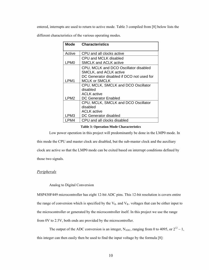
Mode Characteristics
Active CPU and all clocks active
LPM0 CPU and MCLK disabled SMCLK and ACLK active
LPM1
CPU, MCLK and DCO Oscillator disabled SMCLK, and ACLK active DC Generator disabled if DCO not used for MCLK or SMCLK
LPM2
CPU, MCLK, SMCLK and DCO Oscillator disabled ACLK active DC Generator Enabled
LPM3
CPU, MCLK, SMCLK and DCO Oscillator disabled ACLK active DC Generator disabled
LPM4 CPU and all clocks disabled Table 3: Operation Mode Characteristics
Low power operation in this project will predominantly be done in the LMP0 mode. In
this mode the CPU and master clock are disabled, but the sub-master clock and the auxiliary
clock are active so that the LMP0 mode can be exited based on interrupt conditions defined by
those two signals.
Peripherals
Analog to Digital Conversion
MSP430F449 microcontroller has eight 12-bit ADC pins. This 12-bit resolution is covers entire
the range of conversion which is specified by the VR- and VR+ voltages that can be either input to
the microcontroller or generated by the microcontroller itself. In this project we use the range
from 0V to 2.5V, both ends are provided by the microcontroller.
The output of the ADC conversion is an integer, NADC, ranging from 0 to 4095, or 212 – 1,
this integer can then easily then be used to find the input voltage by the formula [8]:
11
Input Voltage = −−+ +− rrr VVV )(4095N ADC (2.1)
Using our given range, (1.1) simply reduces to:
Input Voltage = )5.2(4095NADC V (2.2)
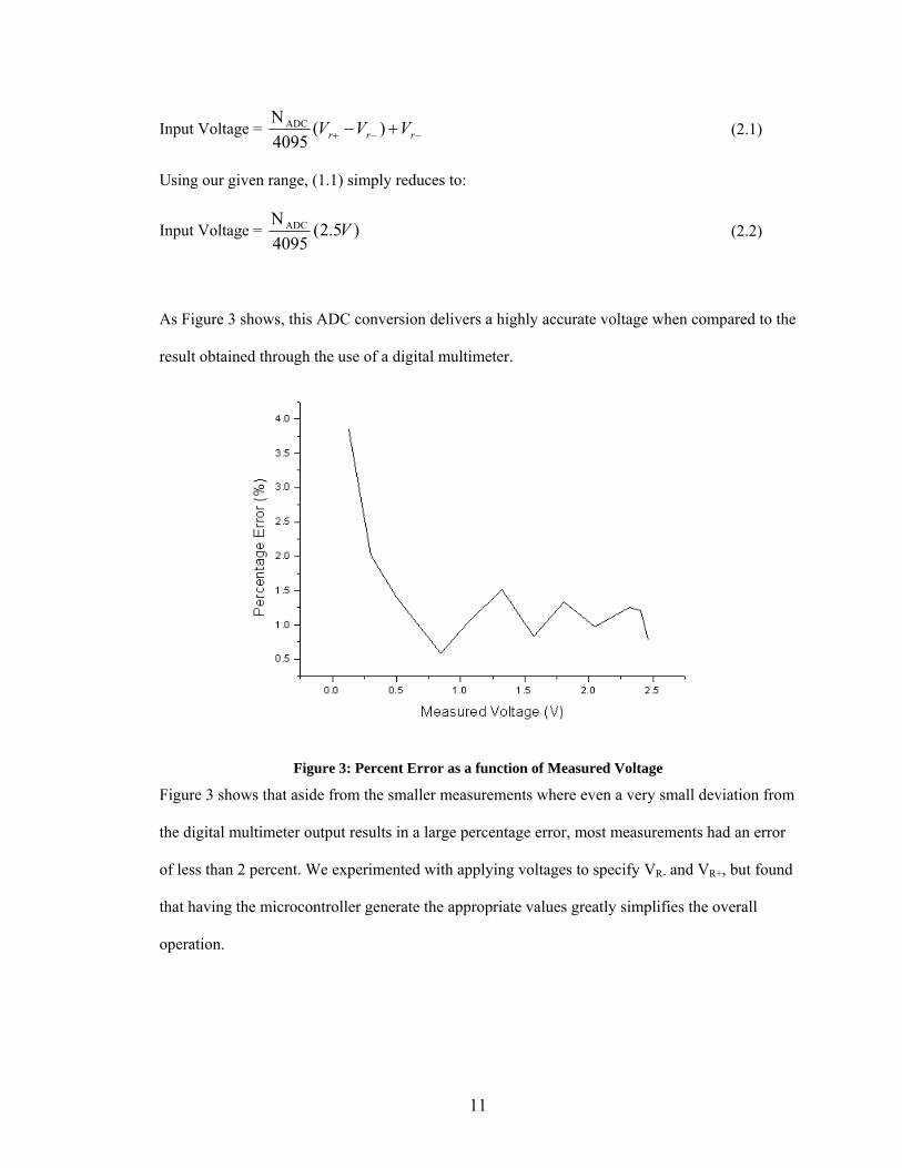
As Figure 3 shows, this ADC conversion delivers a highly accurate voltage when compared to the
result obtained through the use of a digital multimeter.
Figure 3: Percent Error as a function of Measured Voltage
Figure 3 shows that aside from the smaller measurements where even a very small deviation from
the digital multimeter output results in a large percentage error, most measurements had an error
of less than 2 percent. We experimented with applying voltages to specify VR- and VR+, but found
that having the microcontroller generate the appropriate values greatly simplifies the overall
operation.
12
Digital Communication
The MSP430F449 comes with six digital communication ports with each port having eight pins
that can be used for parallel communication. Each of the pins can be read from and written to
independently. Many of the ports have alternate functions, for example, port six is also used for
analog-to-digital conversion. Ports 1 and 2 also have the ability to generate interrupts based on
either high to low or low to high transitions in digital data [8].
The MSP430F449 also allows for two modes of serial communication: UART and SPI.
The SPI mode is a master-slave mode in which data is communicated by multiple devices all
using the same clock provided by the master. The UART mode allows for communication that is
asynchronous to other devices. Instead of sharing a clock, in the UART mode both the transmitter
and receiver operate at the same baud rate. The simplicity associated with not having to have a
shared clock makes the UART mode ideal for all serial communication in this project. Serial
communication will mainly be used for RS232 communication between the receiver and
computer.
A character to be sent or received follows a standard form in which it starts with a start
bit followed by seven or eight data bits, a parity bit, an address bit, and one or two stop bits. All
possible choices in format are set by the appropriate internal register and should obviously be
shared by both the transmitter and receiver. The baud rate used to send the characters is
determined by the clock frequency and internal registers [8].
The UART serial communication mode has two formats: the address bit multiprocessor
format and the idle-line multiprocessor format. The address bit multiprocessor format is typically
used when three or more microcontrollers communicate. The idle-line format is used when two
devices communicate. In our application the microcontroller will be communicating with the
RS232 line so the idle-line format is used.
13
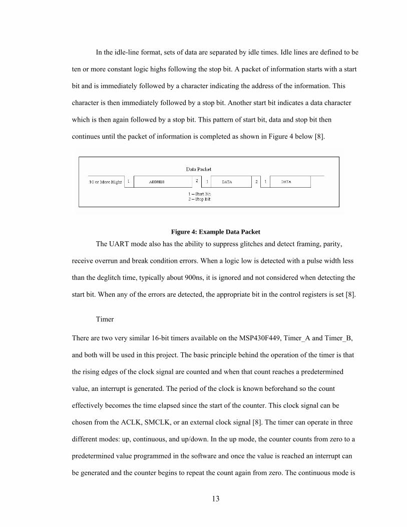
In the idle-line format, sets of data are separated by idle times. Idle lines are defined to be
ten or more constant logic highs following the stop bit. A packet of information starts with a start
bit and is immediately followed by a character indicating the address of the information. This
character is then immediately followed by a stop bit. Another start bit indicates a data character
which is then again followed by a stop bit. This pattern of start bit, data and stop bit then
continues until the packet of information is completed as shown in Figure 4 below [8].
Figure 4: Example Data Packet
The UART mode also has the ability to suppress glitches and detect framing, parity,
receive overrun and break condition errors. When a logic low is detected with a pulse width less
than the deglitch time, typically about 900ns, it is ignored and not considered when detecting the
start bit. When any of the errors are detected, the appropriate bit in the control registers is set [8].
Timer
There are two very similar 16-bit timers available on the MSP430F449, Timer_A and Timer_B,
and both will be used in this project. The basic principle behind the operation of the timer is that
the rising edges of the clock signal are counted and when that count reaches a predetermined
value, an interrupt is generated. The period of the clock is known beforehand so the count
effectively becomes the time elapsed since the start of the counter. This clock signal can be
chosen from the ACLK, SMCLK, or an external clock signal [8]. The timer can operate in three
different modes: up, continuous, and up/down. In the up mode, the counter counts from zero to a
predetermined value programmed in the software and once the value is reached an interrupt can
be generated and the counter begins to repeat the count again from zero. The continuous mode is

14
very similar and can be considered simply an extension of the up mode, but instead of counting to
a value specified in the software it counts to 65,535, or 216 -1, as would be the maximum value
expected in a 16-bit timer. This is also, of course, the highest value the up mode can count to. In
up/down mode the timer counts up to a predetermined value just like the up mode, but instead of
starting at zero again, it decrements the counter to zero. The timer modes used most often are the
up and continuous modes, these will be used in the transmitting microcontroller to control the
digital transmission of the bits to the transceiver and to turn off the board when it has been left
idle for a specified time. The timers also have capture and compare capabilities. When an input is
fed to the timer, the timer can be programmed to copy the contents of the count register at
selected edges of the input signal. When used to compare, the timer can compare the occurrences
of several different interrupts [8].
15
CHAPTER 3: SENSORS
Selection
As discussed earlier, the main goal of the entire board is to perform non-contact length
measurements. To accomplish this we propose a scheme in which the object is placed on the
board and the user uses a hand-held stylus to mark the end point of the object on a number line.
The stylus should not have any wires attaching it to the board or have to touch the sensors which
are placed in a protective covering inside the board.
To accomplish these basic goals we plan to have a linear array of sensors underneath the
number line, when the stylus is brought close to a particular point on the number line, the sensors
underneath identify the position of the stylus. This scheme requires sensors that can, without
mechanical contact, measure the proximity of a stylus. In our case we chose to measure the
proximity of the stylus by inserting a permanent magnet inside of it and measuring the magnet
field emanating from it.
In our search we found two basic types of sensors that can measure magnetic flux density
and can be placed in a linear array: Hall-Effect sensors and magnetorestrictive sensors. Each
produce an electrical output based on the input magnetic flux density. In either case, a
microcontroller will scan the results of all sensors in the linear array to determine the position of
the stylus. Since we strive to design the system out of COTS technology, we choose from readily
available products instead of custom designs.
Although there is a multitude of different characteristics that determine the performance
of a particular sensor, the most important in our case is repeatability. Repeatability specifies
difference between consecutive outputs that are held at identical conditions [10]. In our design, all
the data from the sensors is read by the microcontroller which can adjust the final output for
many types of predictable errors. Since repeatability errors are essentially unpredictable, the
microcontroller cannot adjust for them so the output is directly affected by the error.
16
After repeatability, the next main concern is the reliability of the sensor. The reliability is
defined as likelihood the sensor will function correctly [10]. Since the sensors will be placed
inside the board under a protective layer, any sensor that malfunctions cannot be replaced. This
either forces the user not to measure objects in the vicinity of that sensor or replace the entire
board. In our experience with Hall-Effect sensors, when they do malfunction, the output voltage
with no incident magnetic field density dramatically rises to close to the supply voltage, so
malfunctions are typically easily spotted by the microcontroller and the user can be alerted.
The cost of a sensor is not typically identified as being a characteristic of a sensor, but in
our case it is a major criterion since we hope to build the board as cheaply as possible. Of course
the cost of the sensor is measured not only in how much each individual sensor costs, but also
how many sensors would be required to span the 1m and 2m boards. Furthermore, the current
consumption also indirectly affects the price, since additional current requires a battery which is
typically more expensive.
The non-linear characteristic of the output values is also an important characteristic of the
sensor. If the output of the device can be approximated by a line and still maintain the necessary
accuracy, then interpolation calculations become simpler for the microcontroller. In this context,
interpolation calculations are used to find the location of the magnet when it is not over any
particular sensor. The FMB, however, is calibrated beforehand and a curve for the output can be
found using software such as MATLAB and be programmed into the microcontroller so this
concern is not as major as the previous three. Another somewhat less important concern is the
range of output values for the sensor. A larger range usually implies that changes in the input
magnetic flux density result in larger changes in the output making the overall system more
sensitive to changes in the input. Along with the range, the zero value of the sensor, that is the
output value when there is no input magnetic field must fall in range that can be measured by the
microcontroller.
17
Temperature effects are also normally a serious concern in sensor operation. Most
companies that manufacture sensors do rigorous testing on the performance of their sensors in
different temperature environments so that the microcontroller can use that data coupled with a
temperature sensor to predict any deviations in output value.
As discussed earlier, our two choices for sensing technologies are Hall-Effect sensors and
magnetorestrictive sensors. In a Hall-Effect device, a current is run through a conductor or semi-
conductor material and when a magnetic field is applied a voltage develops that is perpendicular
to both the current and the magnetic field. In physical terms, the incident magnetic field causes a
build up of carriers on one side of the material which creates the potential difference [10]. An
important benefit of Hall-Effect sensors is that they can detect the polarity of the input magnet
field. These sensors then can have their output voltage either increased or decreased from the zero
value.
Magnetorestrictive sensors, on the other hand, produce a change in resistance as a
function of the magnitude of the input magnetic field. The basic physical principle behind
magnetoresistance is the Lorentz force which acts perpendicular to the velocity of the charges and
the magnetic field and tends to force the carriers to move in a circular pattern. This forces more
carriers on one side of the material than the other. Since the carriers are moved to one side of the
material the effective cross-sectional area of the material is reduced, this coupled with the
reduction of carrier speed due to the circular nature of the Lorentz force results in a change in the
resistance. The resistivity of the material is then given by [10]:
Resistivity = VelocityCarrier nsity Carrier De
Voltage×
(3.1)
Typical advantages of magnetoresistive devices are that they can operate at higher frequencies
than Hall-Effect devices, offer greater sensitivity and consume less current [10].
Conventional magnetoresistive and Hall-Effect devices can both deliver repeatability that
is significantly smaller than 1mm accuracy we hope to achieve so both technologies satisfy our
18
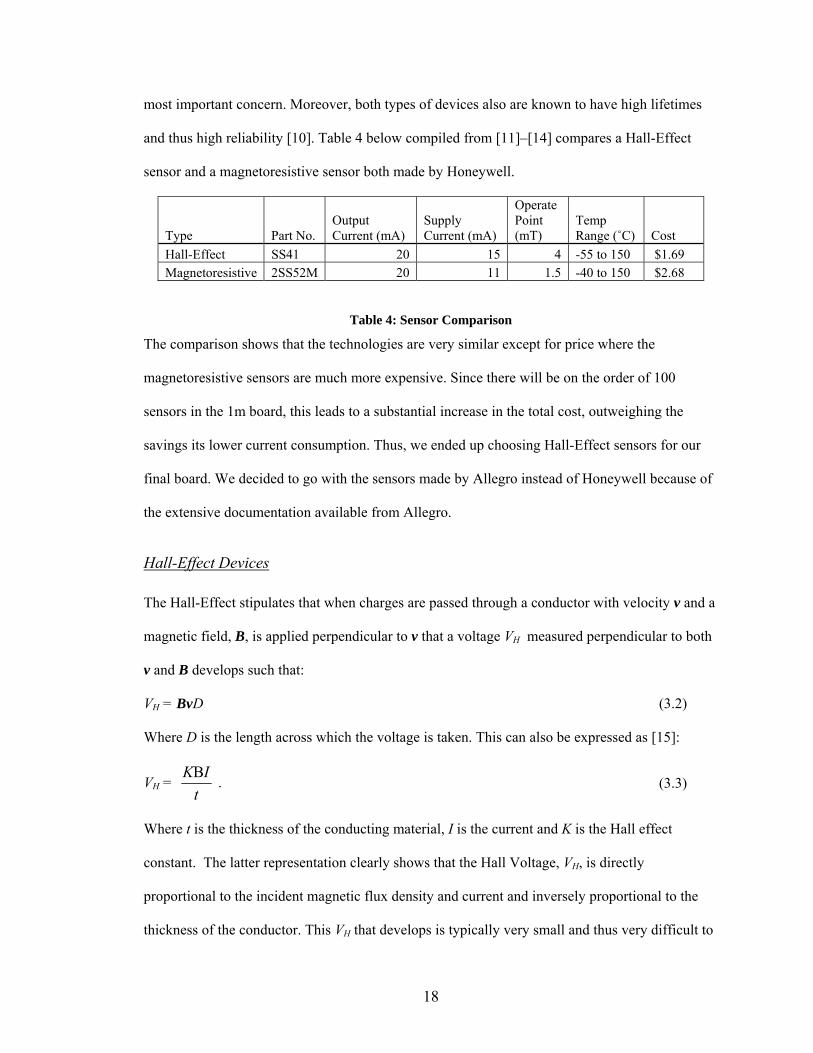
most important concern. Moreover, both types of devices also are known to have high lifetimes
and thus high reliability [10]. Table 4 below compiled from [11]–[14] compares a Hall-Effect
sensor and a magnetoresistive sensor both made by Honeywell.
Type Part No. Output Current (mA)
Supply Current (mA)
Operate Point (mT)
Temp Range (˚C) Cost
Hall-Effect SS41 20 15 4 -55 to 150 $1.69 Magnetoresistive 2SS52M 20 11 1.5 -40 to 150 $2.68
Table 4: Sensor Comparison
The comparison shows that the technologies are very similar except for price where the
magnetoresistive sensors are much more expensive. Since there will be on the order of 100
sensors in the 1m board, this leads to a substantial increase in the total cost, outweighing the
savings its lower current consumption. Thus, we ended up choosing Hall-Effect sensors for our
final board. We decided to go with the sensors made by Allegro instead of Honeywell because of
the extensive documentation available from Allegro.
Hall-Effect Devices
The Hall-Effect stipulates that when charges are passed through a conductor with velocity v and a
magnetic field, B, is applied perpendicular to v that a voltage VH measured perpendicular to both
v and B develops such that:
VH = BvD (3.2) Where D is the length across which the voltage is taken. This can also be expressed as [15]:
VH = t
IKB . (3.3)
Where t is the thickness of the conducting material, I is the current and K is the Hall effect
constant. The latter representation clearly shows that the Hall Voltage, VH, is directly
proportional to the incident magnetic flux density and current and inversely proportional to the
thickness of the conductor. This VH that develops is typically very small and thus very difficult to

19
measure accurately so packaged Hall-Effect devices usually come with some type of amplifying
circuitry built in to raise the voltage levels to a reasonable level [10]. When the Hall-Effect device
is exposed to high fields that often result with a magnet being very close, the device saturates so
there is no increased output voltage for an increase in input flux density. This saturation does not
arise from the Hall-Effect sensor itself, but rather the amplification circuit so the user can be
assured that high fields will not damage the device [16].
The Hall-Effect sensor we chose to use is the Allegro A1321 device. These are three-pin
devices that have a zero voltage that is half of the supply voltage which either increases or
decreases according to whether the South or North pole of the magnet is applied and do not
exhibit dramatic changes in output in different temperatures [17]. Their output is ratiometric, thus
the output voltage is not only proportional to the incident magnet field density but also the supply
voltage [18]. This allows the range of output values to be determined by the supply voltage.
The first concern when operating a Hall-Effect device is that the magnetic flux lines
originating from the magnet must be perpendicular to the face of the device to bring about the
desired change in output [10]. In our case, this requires the stylus to be held perpendicular to the
face of the board to achieve the best results. Moreover, since the calibration of these devices will
be done assuming perpendicular placement of the stylus, any tilt will bring about errors.
The next major concern is the consideration of the total effective air gap (TEAG). Figure
5 from [19] shows that the magnetic flux density is substantially reduced as the TEAG is
increased.

20
Figure 5: Flux Density vs. TEAG
This graph also shows that the relative output voltage decreases dramatically as the TEAG is
increased as would be expected. The TEAG not only refers to the total air gap between the sensor
and the magnet, but rather the total depth between the sensor and magnet. In our case this requires
the protective material covering the sensors to also be included in the TEAG.
In this application we will effectively be measuring the TEAG to determine the proximity
of the stylus. In placing the stylus on the board, the user had three degrees of freedom. Our goal is
only to measure the length, thus the other two degrees of freedom must be constrained to the
calibration procedure. We require, therefore, that the measurement be taken when the stylus is
touching the board to constrain the vertical distance from the sensor and be within the number
tape on the board to constrain the depth, making the horizontal distance the only variable in the
TEAG.
Application
In our application of the Hall-Effect devices, we will be primarily be operating in the unipolar
slide-by mode. That is, one pole will dominate the readings coming from the Hall-Effect sensor

21
and the magnet will be effectively moved from side to side with the components of the TEAG
from the packaging material and stylus predetermined. Given this mode of operation, we expect a
Gaussian curve of voltages with the highest coming when the magnet is directly over the sensor
and the voltages dropping off non-linearly as the magnet is moved horizontally away from the
magnet in either the positive or negative directions [16].
The characterization and verification of a Gaussian characteristic of the sensors was done
by Abhinav Pathak. There were several characterizations done to ensure the predicable behavior
of the output voltages, one of these characterizations are shown below in Figure 6.
-20 -15 -10 -5 0 5 10 15 20
2.5
3.0
3.5
4.0
4.5
5.0
Output Voltage vs. Displacement From Center
Vol
tage
(V)
Displacement (mm)
Figure 6: Initial Characterization
In this initial characterization the magnet is held a fixed distance vertically from the sensor and
displaced in the horizontal direction. Figure 6 illustrates the expected Gaussian shape, but also
shows that as the magnet tends to saturate the sensor as it gets very close. In later
characterizations and the final implementation we will alter the TEAG and magnet strength to
avoid this saturation. Furthermore, when the sensors are actually implemented with the

22
microcontroller we find it advantageous to use the North Pole instead of South Pole so that the
voltages drop from the zero value.

23
CHAPTER 4: WIRELESS TECHNOLOGY
Digital Modulation
The three main digital modulation schemes that were considered for this project are
amplitude shift keying (ASK), frequency shift keying (FSK), and phase shift keying (PSK). All of
these schemes will be used in their binary implementation so that each modulation scheme will
deliver a distinct signal corresponding to either a logic high or a logic low. Typically ASK
consists of the carrier signal being turned on or off depending on the input binary sequence. In
this sense ASK is also known as on-off keying (OOK). Binary FSK consists of a sinusoidal
carrier whose frequency is adjusted to according to the input binary data. Binary PSK consists of
a carrier whose phase is shifted between two different values to reflect the binary data. In practice
these phases are usually 0 and π [20].
The two main criteria used to judge between different modulation schemes in this project
are the probability of error in the presence of additive white Gaussian noise (AWGN) and the
ease of implementation. Performance in AWGN is often used a performance metric to compare
different modulation schemes. The ease of implementation is important because it helps to
determine the diversity of products that implement that scheme. The eventual choice will also be
judged on a variety of hardware criteria, so it helps to have a diverse set of technology to choose
from.
The performance of the different modulation schemes in AWGN is computed using an
optimum receiver based on the maximum likelihood rule. In all cases synchronous detection is
used to compare the schemes. For OOK the probability of error, Pe, can be shown to be [20]:
Pe = 21
erfcon
E4
b. (4.1)
24
Where Eb is the bit energy defined as the energy of the input binary signal over one bit period and
no is defined as the integration of the noise voltage over one bit period. Thus, the probability of
error then is a function of Eb/no which is defined as the signal to noise ratio (SNR) per bit. Next,
for FSK the probability of error can also be shown to be a function of the SNR per bit [20]:
Pe = 21
erfcon
E2
b. (4.2)
Lastly, the probability of error in the case of PSK can be shown to be [20]:
Pe = 21
erfcon
Eb. (4.3)
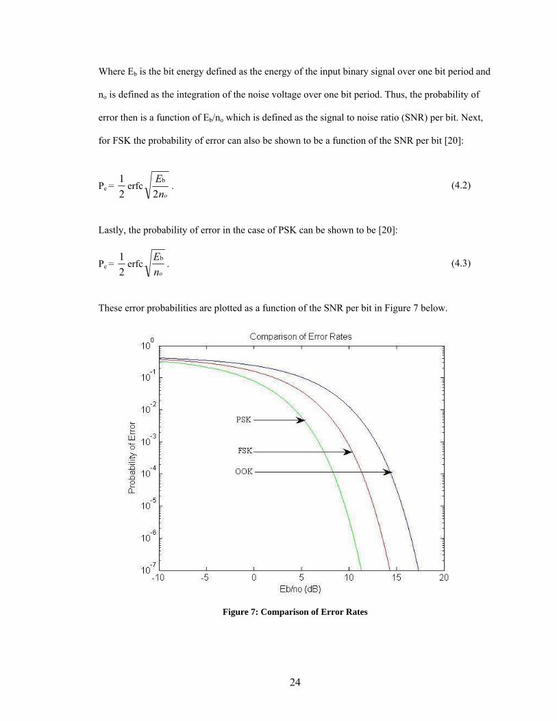
These error probabilities are plotted as a function of the SNR per bit in Figure 7 below.
Figure 7: Comparison of Error Rates
25
As expected, the probability of error with all the modulation schemes decreases as SNR per bit
increases. Figure 7 clearly shows that PSK performs the best in the presence of AWGN, followed
by FSK and ASK. The next criterion used to judge between modulation schemes is the ease of
implementation. OOK is the easiest to implement since it simply involves turning on and off the
carrier based on the binary data. OOK also does not require coherent demodulation and can
simply be demodulated using the received signal strength indication (RSSI). FSK is also simple
to implement as it can be generated coherently using an IQ modulator or incoherently using a
phase locked loop. Also since the signal has constant amplitude, a non-linear power amplifier can
be used in the transmitter circuit. Lastly, PSK is more complex to generate because it requires
coherent modulation [21].
Considering both the error probabilities and the complexity of implementation we chose
FSK as our modulation scheme. This scheme provides better performance than ASK in the
presence of AWGN yet still is relatively simple to implement so that there is a diverse set of
technologies to choose from. Our eventual choice in transceiver technology, the basis for which
will be discussed later, is the TRF6903 transceiver. The transceiver modulates the signal using a
phase locked loop which produces signal with a frequency deviation of 32 KHz, thus a 64 KHz
difference between the two signals. The baseband signal is coded using non-return to zero (NRZ)
coding which doubles the maximum achievable data rate when compared to Manchester coding
[22] and has been experimentally shown to have fewer errors in wireless transmission in a device
similar, the TRF6900A, to the TR6903 [23].
Selection of the Operating Frequency
The selection of the frequency band is one of the most important decisions in the wireless
system design as it often dictates possible choices in transceiver and antenna technology. The
frequency bands that were considered are the 902-928 MHz and the 2.4-2.48GHz Industrial,
Scientific and Medical (ISM) bands. Higher frequencies tend to allow for more bandwidth thus

26
allowing for higher data rates. It should be noted, however, that data rate is not a primary concern
in this project since this is not a high speed application requiring large amounts of data to be sent
over the wireless link. A selection of lower frequency is supported by the fact that antenna gain at
its resonant frequency normally increases with frequency. This increased gain implies that the
wave emanating from the antenna does not spread out as much, thus reducing its ability to
navigate around obstacles in a NLOS environments. After considering all of the options, we
chose the 902-928MHz band since data rates are not pivotal in this project and communication in
this band generally performs better than the 2.4-2.48GHz band in NLOS environments [20].
Transceiver Selection
The function of the transceiver, or a transmitter/receiver pair, is to take digital data on transmitter
side and convert it to an analog waveform fit for wireless transmission and to perform the
complementary action on the receiver side. The selection criteria include the modulation
technique, sensitivity, maximum output power and maximum data rate. Similar to the
microcontroller selection, ease of implementation is also a concern. Documentation regarding the
operation of the device and more importantly the simplicity in the integration with our chosen
microcontroller is important. We again restrict ourselves to readily available technology in so that
we can design the entire product out of COTS technology. This restricts us from designing a
custom transceiver for this specific application. We have already chosen to use FSK modulation
so we are obviously biased towards choosing a device that has FSK capability. The next
consideration is the sensitivity which is defined as minimum input signal that can be converted to
a meaningful voltage by the receiver [20]. This is a major concern for our project because the
FMB will often be operated in severe conditions. On the other hand, we would also like to deliver
as strong a signal as possible to receiver since , as was shown earlier, error rates tends to decline
as the signal to noise ratio increases. Furthermore, we also would like to be able to adjust the
output power based on application, increasing the power when conditions require while saving
27
battery life by reducing the output power in more hospitable environments. Lastly, the maximum
data transfer rate is obviously a concern in designing any wireless system but as discussed earlier,
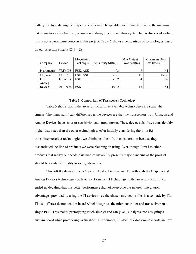
this is not a paramount concern in this project. Table 5 shows a comparison of technologies based
on our selection criteria [24] - [28].
Table 5 shows that in the areas of concern the available technologies are somewhat
similar. The main significant differences in the devices are that the transceivers from Chipcon and
Analog Devices have superior sensitivity and output power. These devices also have considerably
higher data rates than the other technologies. After initially considering the Linx ES
transmitter/receiver technologies, we eliminated them from consideration because they
discontinued the line of products we were planning on using. Even though Linx has other
products that satisfy our needs, this kind of instability presents major concerns as the product
should be available reliably as our goals indicate.
This left the devices from Chipcon, Analog Devices and TI. Although the Chipcon and
Analog Devices technologies both out perform the TI technology in the areas of concern, we
ended up deciding that this better performance did not overcome the inherent integration
advantages provided by using the TI device since the chosen microcontroller is also made by TI.
TI also offers a demonstration board which integrates the microcontroller and transceiver on a
single PCB. This makes prototyping much simpler and can give us insights into designing a
custom board when prototyping is finished. Furthermore, TI also provides example code on how
Company Device Modulation Technique Sensitivity (dBm)
Max Output Power (dBm)
Maximum Data Rate (kb/s)
Texas Instruments TRF6903 FSK, ASK -103 8 64 Chipcon CC1020 FSK, ASK -121 10 153.6 Linx ES Series FSK -102 4 56 Analog Devices ADF7025 FSK -104.2 13 384
Table 5: Comparison of Transceiver Technology
28
to execute wireless communication which simplifies the writing of our own code for this project.
So in the end, we chose to use the TRF6903 transceiver from TI.
RF Circuitry
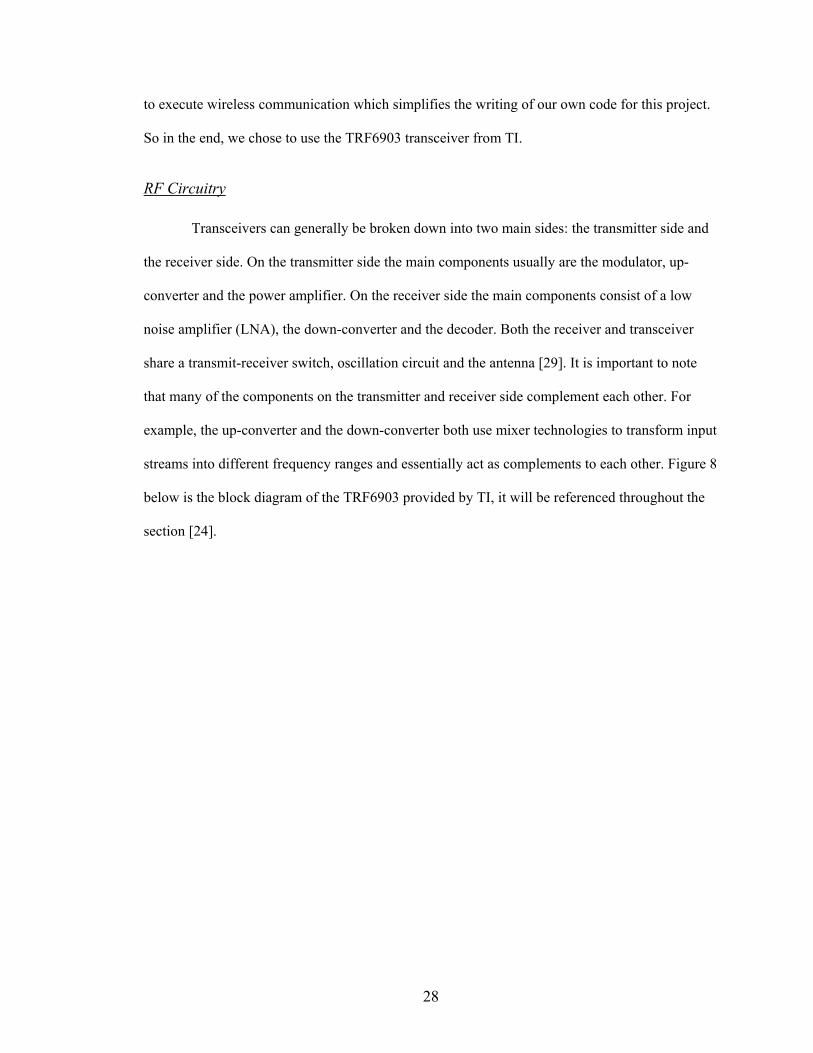
Transceivers can generally be broken down into two main sides: the transmitter side and
the receiver side. On the transmitter side the main components usually are the modulator, up-
converter and the power amplifier. On the receiver side the main components consist of a low
noise amplifier (LNA), the down-converter and the decoder. Both the receiver and transceiver
share a transmit-receiver switch, oscillation circuit and the antenna [29]. It is important to note
that many of the components on the transmitter and receiver side complement each other. For
example, the up-converter and the down-converter both use mixer technologies to transform input
streams into different frequency ranges and essentially act as complements to each other. Figure 8
below is the block diagram of the TRF6903 provided by TI, it will be referenced throughout the
section [24].
29
Figure 8: RF Transceiver Block Diagram
The TRF6903 transceiver has a multitude of options that can be set for various aspects of
transmission and reception. These choices are set by the microcontroller through the serial
interface. Before the start of the transmission, the microcontroller sends data to the transceiver to
program the program words. The transceiver has five program words which can be used to set
choices such as desired output power, modulation scheme and whether the transceiver is in
reception or transmission mode [24].
Modulator/Demodulator
The first component on the transmitter side is the modulator. The modulator converts the
incoming digital data stream into an analog waveform specified by the modulation scheme. It also
increases the frequency of the entire stream to an intermediate frequency (IF) or in some cases all
30
the way to the transmission frequency. In the case that the modulator takes the stream to an IF
frequency, the stream will later be converted to the band of choice later by an up-converter. The
modulation in the TRF6903 is done by a phase-locked loop (PLL) which delivers the modulated
signal at the desired transmit frequency, approximately 915MHz, without the need of an
additional up-converter. The demodulator decodes the modulated received analog signal back to
the original digital data signal. The TRF6903 uses a quadrature demodulator to demodulate the
signal. As the block diagram indicates, the demodulator takes its input from the limiter.
Mixer
Up and down conversion of frequency are complementary operations that can both be
accomplished using a mixer. In this project, only the down conversion is actually done by the
mixer, the PLL serves to deliver a modulated output at the desired frequency for transmission. An
ideal mixer produces an output that is proportional to the product of the inputs. When performing
down-conversion, the inputs to the mixer are the RF input signal and a signal at the local
oscillator frequency delivered by internal circuitry, in this case the PLL. Both of the signals can
be simplified and viewed as pure sinusoids and represented as [20]:
VRF (t) = cos(2ΠfRFt) (4.4) VLO (t) = cos(2ΠfLOt). (4.5) Then the output is the product of the two input signals with an additional constant term
introduced as a result of voltage loss in the operation of the mixer, it can be represented as:
VOUT = A cos(2ΠfRFt) cos(2ΠfLOt). (4.6) Using simple trigonometric identities, the output signal can be viewed as:
vOUT = 2A
[ cos(2Πt(fRF - fLO) + cos(2Πt(fRF + fLO)]. (4.7)
Thus the output frequency of the transmission is then simply:
31
fOUT = fRF ± fLO.. (4.8) The desired frequency is the difference between the two frequencies which is selected using a low
pass filter. Since the LO and RF frequencies are very close together, their sum and difference are
then relatively far apart so that filtering out the sum signal can be done easily.
For ideal mixer operation, impedances at all three ports of the mixer should be matched.
In many technologies, however, that is not the case. This leads to loss in output power, known as
conversion loss. Matching can be done through the use of resistors with real impendence or
reactive components such as capacitors and inductors which have imaginary impedance.
Adequate matching can be difficult in many cases since resistors dissipate power thus leading to
overall loss and reactive components used in matching are typically highly frequency dependent.
Although conversion loss is a reality for many mixer technologies, some technologies actually
boast a conversion gain. Usually diode mixers have losses in the range of 4 to 7 dB and transistor
mixers can deliver some gain [20]. The combination of the LNA and the mixer in the TRF6903
has a conversion gain of 18 dB [24]. The values for the LNA and mixer are given together since
they work so closely together in the transceiver.
Another figure of merit relating to mixers is the noise figure. Noise figure is typically
defined as [29]:
Outputat SNRInputat SNR
=F [dB]. (4.9)
The combination of the LNA and the mixer in the TRF6903 has a single side band noise figure is
6.5 dB so the double side band noise figure then is 13 dB, including the external matching
network [24].
Amplifiers
Typically there are two general types of amplifiers that must be used in transceiver
design. The first is a traditional power amplifier which is used on the transmitter side to amplify

32
the signal before it is transmitted. The second type of amplifier, a low noise amplifier (LNA) is
used to amplify the received signal. At full utilization, the TRF6903’s power amplifier delivers 8
dBm (or about 6.31mW) of output power to a matched 50Ω load. The power amplifier also has
the ability to attenuate the output power by either 10dB or 20dB resulting in -2dBm (0.631mW)
and -12dBm (0.0631 mW) output power to a matched load respectively. When the power
amplifier is disabled, the output power delivered to a matched load is -80dBm (10-8 mW) [24].
This attenuation value is set by the microcontroller through the appropriate program words in the
transceiver. In this project we normally output full power. The power amplifier is only activated
during transmission since the current consumed and thus the power consumed rises significantly
with the power amplifier active. When all other components are active but the power amplifier is
disabled, the transceiver normally consumes 10mA of current, while when the power amplifier is
active at full power in addition to all the other components the typical current consumption jumps
to 35mA [24].
In receiver systems where there are generally low losses after the first amplifier, the noise
figure of the entire system is most significantly affected by the performance of the first amplifier
so a low noise amplifier is used. The output of the LNA is then fed directly to the mixer. In the
TRF6903, the conversion gain of the LNA/mixer system is specified together since they work so
closely together. The conversion gain of the system is 18dB and the SSB noise figure is 6.5dB.
After passing through this stage, the frequency of the data is at the IF frequency, or 10.7MHz.
This signal is then fed to a 10.7MHz discriminator and then to a limiter that has a gain of 86dB
and a noise figure of 4dB. Finally this output is sent to the demodulator.
Oscillation Techniques Many of the RF components in a typical transceiver need a dependable input frequency. One
method of delivering such a known frequency is through the use of crystals that oscillate due to
the piezoelectric effect. When a voltage is applied across the faces of the crystal, forces are
applied to bound charges which result in a vibration at a resonant frequency [29]. The reference
33
crystal used in this application is the Crystek 017119 which outputs a signal at 19.7MHz.
Multiples of this frequency is provided by a phase-locked loop (PLL) which takes a crystal
oscillator as an input and outputs a signal with multiples of that frequency with noise and stability
specifications similar to those of the highly accurate crystal oscillator [30].
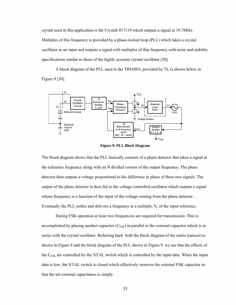
A block diagram of the PLL used in the TRF6903, provided by TI, is shown below in
Figure 9 [30].
Figure 9: PLL Block Diagram
The block diagram shows that the PLL basically consists of a phase detector that takes a signal at
the reference frequency along with an N divided version of the output frequency. The phase
detector then outputs a voltage proportional to the difference in phase of these two signals. The
output of the phase detector is then fed to the voltage controlled oscillator which outputs a signal
whose frequency is a function of the input of the voltage coming from the phase detector.
Eventually the PLL settles and delivers a frequency at a multiple, N, of the input reference.
During FSK operation at least two frequencies are required for transmission. This is
accomplished by placing another capacitor (CFSK) in parallel to the external capacitor which is in
series with the crystal oscillator. Referring back both the block diagram of the entire transceiver
shown in Figure 8 and the block diagram of the PLL shown in Figure 9, we see that the effects of
the CFSK are controlled by the XTAL switch which is controlled by the input data. When the input
data is low, the XTAL switch is closed which effectively removes the external FSK capacitor so
that the net external capacitance is simply:
34
Cnet = Cexternal. (4.10)
The output frequency (flogic low) then is based only on the single external capacitor and the crystal
oscillator. When the input data is high, the XTAL switch is open which gives the net external
capacitance:
Cnet = Cexternal + CFSK. (4.11) The output frequency (flogic high) then is based on both capacitors [24]. In addition to serving as the
modulator, during reception the PLL also delivers the LO frequency to the mixer that is used for
down conversion. In the receive mode the XTAL switch is closed so that a constant frequency is
delivered to mixer.
Data Slicer and Bit Synchronizer
Before discussing the operation of the data slicer and bit synchronizer, it is instructive to look at
the basic structure of a wireless packet. The packet starts off with a training sequence of
alternating logic highs and lows that is used to train the internal components of the transceiver.
After the training sequence, a start bit is sent that is three times the length of a normal bit to
indicate that the training sequence has ended and data is about to begin. Lastly, the data is sent
and the transmission is completed.
The purpose of the data slicer is to take data coming from the demodulator and output
digital data to match the data originally sent by the transmitter. This is accomplished by
comparing the output of the demodulator to a reference voltage. The reference voltage is set by
the sample-and-hold (S&H) capacitor. During learn mode the S&H capacitor charges to the
average value of the training sequence. After the training sequence is completed, the transceiver
switches from learn to hold mode where it holds the S&H capacitor voltage and uses it to
decipher the signal coming from the demodulator. The value of the S&H capacitor is given by
[24]:
35
CSH = (Hz)) in (Data Rate51k5
BitsTraining of #∗∗
. (4.12)
The time constant of the S&H capacitor is determined by factoring in an internal 51kΩ resistor.
Thus the time constant is:
τ = BitsTraining of #
Hz)in (Data Rate5∗. (4.13)
This time constant then also then puts constraints on the duration of the incoming RF signal. As
the voltage level of the S&H capacitor decays, the data slicer looses the ability to accurately
decipher between logic highs and lows. In our project we use a 5.6nF capacitor for CSH.
The bit synchronizer ultimately recovers the data at a predetermined frequency. The
predetermined frequency is a function of the crystal and values provided by the microcontroller.
The transceiver provides both the final received data at the RX_DATA terminal and the
corresponding clock at the DCLK terminal as shown in the block diagram in Figure 8.
Reception Modes
Depending on the needs of the user, the TRF6903 can operate in one of four reception modes.
When operating in the raw data mode the output of the data slicer is directly fed to the output
terminal RX_DATA and the bit synchronizer is completely bypassed. In the Deglitch mode, the
output of the data slicer is fed to a deglitch filter. If five or more of the last seven samples taken
are logic highs, then the filter outputs a high, and if two or fewer of the last seven samples are
logic highs then the filter outputs a low. If neither one of the conditions apply the value is kept the
same. The frequency by which the filter samples that output of the slicer is programmed by the
microcontroller. The clock used to sample the slicer data is provided at the DCLK terminal and
the deglitched data is provided at RX_DATA [24].

36
In clock recovery mode, the output of the deglitch filter is synchronized to a bit-rate
clock. For the clock recovery mode to deliver the desired synchronous data the number of
consecutive logic highs or logic lows, NC, must meet the condition:
NC < Δ
250000 . (4.14)
Where Δ represents the error between the transmit bit rate and the receiver bit rate measure in
parts-per-million (ppm). The deglitched data is outputted at the RX_DATA terminal and the
synchronous bit-rate clock is outputted at the DCLK terminal [24].
The last mode of operation is the self train mode where the transceiver also looks for the
end of the training sequence in addition to performing clock recovery. The transceivers being
used in this project operate in the self train mode. The outputs at the RX_DATA and the DCLK
terminal are identical to those when the transceiver is in the clock recovery mode but in the self
train mode the RX_FLAG terminal is raised to logic high for one clock cycle at the first bit not
within the training sequence [24].
Basic Antenna Facts
The antenna is the final piece of hardware on the transmitter side and the first piece of hardware
on the receiver side. On the transmitter side the antenna is takes an electrical signal and converts
it to an electromagnetic wave which propagates to the receiver side. On the receiver side, the
antenna performs the complimentary action by converting the incoming electromagnetic wave to
an electrical signal. By the Lorentz reciprocity theorem we find that the same antenna can be used
for transmission and reception [31].
The radiation pattern of an antenna shows the strength of the field emanating from the
antenna as a function of either the azimuthal angle, φ, or the elevation angle, θ [20]. By the
reciprocity theorem, this radiation pattern also shows how well the antenna receives in each
direction.
37
The directivity of an antenna is a quantitative description of the radiation pattern. The
directivity, D, of an antenna is defined as [31]:
angle solidunit per radiatedpower Averageangle solidunit per radiatedPower ),( =φϑD . (4.15)
Or equivalently as:
r
r
PdP
4),(Ω
Π=d
D φϑ (4.16)
where Pr is defined to be the total radiated power. Manufactures often refer to the maximum
directivity simply as the directivity [31]. A high directivity cited by the manufacturer then implies
that the electromagnetic wave emanating from the antenna is tightly confined and highly
directional. The gain of an antenna is a closely related parameter that also takes into account the
efficiency, e, of the antenna which is defined as being [20]:
in
r
PP
=e (4.17)
where Pin is defined as being the total input power. The gain, G, of an antenna then is [20]:
).,(),( φϑϕϑ eDG = (4.18) An important receiving characteristic of an antenna is how much of the incident power is
received by the antenna. This total received power can be expressed as [20]:
avger SAP = (4.19)where Savg is the time average of the incident electromagnetic wave’s Poynting vector and Ae is
the effective area of the antenna. This area can be thought of being the effective area that captures
the incoming information bearing wave. It can be shown that under matched impedance and
polarization conditions, the effective area Ae can be expressed as [31]:
),(4
20 φϑ
λGAe Π
= (4.20)
where 0λ is the operating wavelength of the antenna. We are operating in the 902-928MHz
frequency band so the characteristic wavelength is approximately 33cm.
Another critical parameter of an antenna is its impedance. This impendence determines
the amount of power that will be delivered to the antenna. If the impedances of the transmission
38
line and antenna are not matched, some of the power will be reflected rather than fed to the
antenna resulting in a reduction of the efficiency of the transmitting system.
Antenna Choice
In addition to the inverted-F PCB antenna that comes with the TI demonstration board, we also
considered using a dipole antenna. In choosing the antenna we require that the antenna be able to
be adjusted by the user to reduce the effects of polarization mismatch. This freedom in this
azimthual and elevation directions allows for an optimal relative configuration of the transmitting
and receiving antennas irrespective of the relative orientation of the FMB and the receiver. We
also require the antenna be a nearly omnidirectional in the azimuthal direction as we would like to
make the operation as simple as possible by not requiring a specific orientation for the antennas in
the azimuthal direction.
In the end we chose a half-wave dipole antenna, the PSKN series, made by Mobile Mark.
This antenna comes with a knuckle that allows its orientation to easily be changed as we had
earlier stipulated. Furthermore, the dipole antenna has a predictable and an omnidirectional in the
azimuthal direction making it easier to use for both users on the FMB and receiver side. It can be
shown that the directivity of a half-wave dipole antenna is given by [31]:
.sin
cos)2cos((64.1),(2
⎟⎠⎞
⎜⎝⎛ Π
=ϑ
ϑφϑD (4.21)
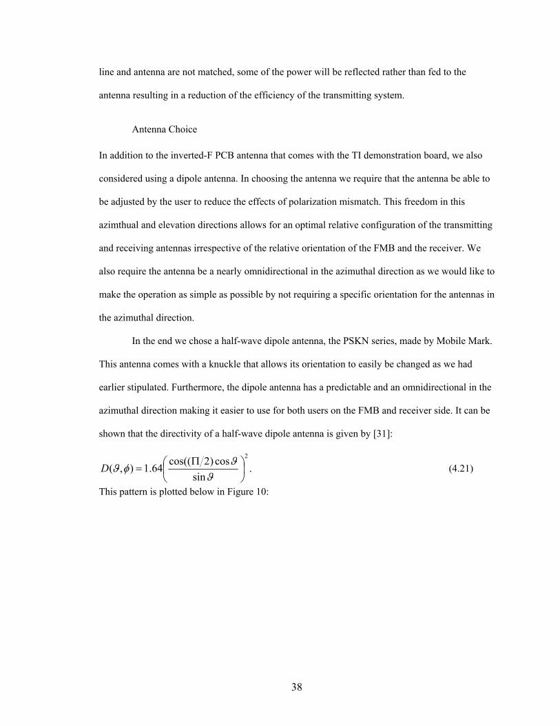
This pattern is plotted below in Figure 10:
39
Figure 10: Typical Half-Wave Dipole Radiation Pattern
Figure 10 shows that the antenna radiates and receives best along the y-axis and has a minimum
transmission and reception along the z-axis. This shows that antenna should be oriented vertically
rather than horizontally for optimum transmission. The PSKN series antenna has a maximum gain
of 1.70 in the 870-960MHz band [32]. The PSKN series antenna also has an impedance of 50Ω
which also is the impedance of the transmission line that feeds the antenna thus assuring no
power is reflected back. Using (6.6) with a maximum gain of 1.70 we find that the maximum
aperture is 0.39m2.
Radio Propagation
Once the antenna radiates the electromagnetic wave, this information carrying wave must
propagate through the communication channel during which it can be subject to a variety of
effects that can impact its characteristics. The main propagation effects for communication in our
frequency band are reflections, diffraction, scattering, attenuation and Doppler spread [20].
The effect of each of these factors depends heavily on the environment and application of
the particular wireless device. Our goal is to design this device to work in all environmental
conditions that fisheries researchers may encounter, thus we must plan for outdoor propagation in
all types of weather conditions as well as indoor propagation. We assume this indoor environment
to have various non-metallic obstacles blocking the line-of-sight.
40
Based on the conditions we expect to operate in, we make several assumptions. First we
assume that the FMB and the receiver will not be moving relative to each other so Doppler shift
will not be an important concern for us. Likewise, we also assume there will be no scattering
objects such as foliage in the channel and no edges or corners that may cause significant
diffraction. Our main concerns, then, are attenuation in the channel due to weather conditions and
reflections from within their environment either indoor or outdoor. All of these channels effects
tend to reduce the signal power from what would be expected in free-space propagation, thus
reducing the signal to noise ratio which has been shown earlier to increase error rate.
The effects of reflections manifest themselves most when there is an absence of a line of
sight between the board and the receiver resulting in a fading environment. Fading is a small-
scale effect in which relatively small variations in distance result in large variations, 20-30dB in
severe cases, in the received signal [20]. To ensure that our wireless link can operate effectively
in a reflective environment, we make sure to test in a situation where there are multiple reflectors
such as walls, desks and appliances and no line of sight. The results of these tests will be
discussed later.
The other main effect is the attenuation due to weather conditions. In our case, we will
have to plan for the attenuation effects of rain, ice and snow. The most substantial attenuation at
our operating frequency is caused by rain. Although rain can cause scattering, the attenuation
mostly derives from the fact that water has a complex permittivity and thus can be considered a
lossy dielectric [31]. In general, the attenuation from rain depends on the rate of rainfall,
operating frequency and temperature. These effects can be summed up in the equation [31]:
baRA = dB/km (4.22)
where R is the rate of rainfall in millimeters per hour, and the constants a and b depend on
temperature and frequency. In our case, for heavy rain which corresponds to about 16 mm/hr
[31], at 0°C we get an attenuation of -410 5.46× dB/km which obviously does not result in a

41
significant decline in signal level at the receiver. So we conclude that main concern in the
propagation is reflections from various elements in the environment of the FMB and the receiver.
In our testing procedure we will then test the link in an environment prone to multiple reflections
rather than an anechoic chamber.
42
CHAPTER 5: IMPLEMENTATION AND TESTING
System Design and Implementation
The operation of the entire system can be broken down into three main stages: length
measurement, wireless transmission and reception. Each of these segments performs a distinct
function and has a microcontroller dedicated to its operation. The length measurement segment
finds the location of the stylus and passes that information along with other parameters to the
transmitting microcontroller that programs the transceiver and sends it the data to be transmitted.
The transceiver then wirelessly sends the data to a transceiver on the receiver side. The receiving
microcontroller then takes the data coming from the receiving transceiver and sends it to the
computer on the receiver end through the RS232 port. The code for the length measuring,
transmitting, and receiving microcontrollers can be found in Appendices A, B, and C
respectively.
The basic schematics shown in Figure 11 and Figure 12 show how the different elements
of the system interact, they will be referenced throughout this section.
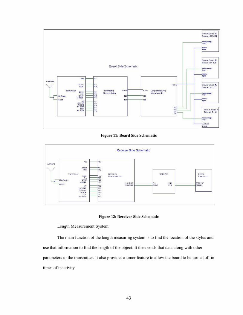
43
Figure 11: Board Side Schematic
Figure 12: Receiver Side Schematic
Length Measurement System
The main function of the length measuring system is to find the location of the stylus and
use that information to find the length of the object. It then sends that data along with other
parameters to the transmitter. It also provides a timer feature to allow the board to be turned off in
times of inactivity

44
The basic length measurement scheme is to measure the output voltage of all of the
sensors, when the output of one of the sensors changes, the microcontroller finds the sensor that
changed to determine the length. The course position of the sensor is simply corresponds to the
identity of the sensor whose output value changes the most. Since the sensors are spaced 6mm
apart, this gives us an accuracy of ± 3mm. After the measurement is taken, the microcontroller
uses a polynomial that describes the position of a magnet as a function of output value derived
from calibration data to find the fine position accurate to 1mm as required.
In practice, the Allegro 1321 Hall-effect sensor has a zero voltage that is half of the
supply voltage. The sensor is also known to have approximately linear operation with respect to
the input flux density when the supply voltage ranges from 4.5V to 5.5V. Though the linearity
does not hold with respect to the distance to magnet, since the flux density of a magnet is non-
linear with respect to distance to the measuring point, we decided to stay in this range to try to
make the calibration as simple and accurate as possible. Operation outside of this range would
require working in a regime that is non-linear with respect to input flux density which then would
lead to a higher degree of non-linearity with respect to distance. This added non-linearity would
make it more difficult to calibrate the sensors accurately. The microcontroller works on a separate
supply voltage of about 2.54V and should not take any inputs more 0.3V higher than its supply
voltage [5], so we chose a supply voltage 4.5V which corresponds to a zero voltage of about
2.25V, well within the range for the microcontroller. We also chose to use the North Pole of the
magnet to force the output voltage to fall from the zero value for the same reason.
Once the board is turned on, the microcontroller begins to continually scan all the
sensors’ outputs by providing a digital address to a series of 8-to-1 analog multiplexers and
reading their output. In the current implementation we have one PCB module consisting of 42
sensors spanning about 25cm. For a 1m long board, we would then have to use four of these
modules. Each of these modules has seven total analog multiplexers, six of these multiplexers are
the considered level 1 multiplexers that are directly tied to seven sensors each and one level 2
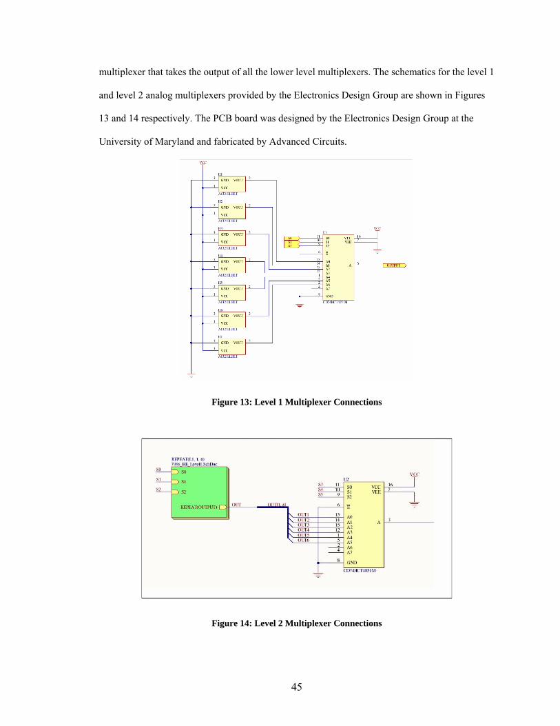
45
multiplexer that takes the output of all the lower level multiplexers. The schematics for the level 1
and level 2 analog multiplexers provided by the Electronics Design Group are shown in Figures
13 and 14 respectively. The PCB board was designed by the Electronics Design Group at the
University of Maryland and fabricated by Advanced Circuits.
Figure 13: Level 1 Multiplexer Connections
Figure 14: Level 2 Multiplexer Connections

46
As the general schematic diagram in Figure 11 shows, the addresses that are fed to the
analog multiplexers come from Port 3 of the microcontroller. The first three pins are tied to the
address lines for all the level 1 analog multiplexers, while the next three pins are tied to level 2
multiplexers. The output of each of the level 2 analog multiplexer’s are then tied to an ADC pin,
the microcontroller has eight total pins to be used for this purpose. Overall this implements a
basic coordinate system, for instance if the first three pins give an address of 5 and the next three
give an address of 3, then the sixth sensor of the fourth analog multiplexer is selected from each
of the modules to be read by its ADC pin. The results from the ADC pins are then converted into
voltages through the use of equation (2.2).
We configure the ADC to operate based on the MCLK which has a frequency of
2.46MHz. For each conversion, the ADC spends 8 cycles sampling the voltage and 13 cycles
performing the conversion. Thus each conversion takes approximately 8.5 μs and an entire scan
of the module takes about 0.4ms.
During normal operation when there are no appreciable changes in the output values of
the sensors, the microcontroller simply repeatedly scans all the sensors’ output voltages,
overwriting the values of the previous scan. When a sensor reacts to magnetic field and its value
drops below a set trigger value another measurement scheme is triggered. As soon as the value of
one or more sensors drops below the set trigger value and a scan is complete, the microcontroller
finds the sensor with lowest output voltage and the second lowest output voltage. We assume the
location of the lowest output to be the course position of stylus. For the next 32 voltage
measurements, the value of the most affected sensor is read into separate array in addition to the
normal scanning. To match the values obtained from a calibration, we need the minimum value of
the output voltage, i.e. the output value when the stylus actually touches the board as stipulated.
After the 32 measurements are completed, the microcontroller finds the minimum voltage which
is the value used to find the fine position. Figure 15 shows a typical voltage characteristic with a
trigger value of 1.5V.
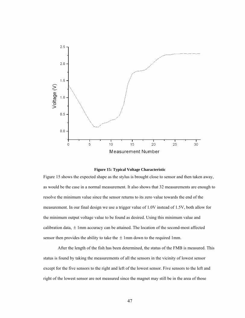
47
Figure 15: Typical Voltage Characteristic
Figure 15 shows the expected shape as the stylus is brought close to sensor and then taken away,
as would be the case in a normal measurement. It also shows that 32 measurements are enough to
resolve the minimum value since the sensor returns to its zero value towards the end of the
measurement. In our final design we use a trigger value of 1.0V instead of 1.5V, both allow for
the minimum output voltage value to be found as desired. Using this minimum value and
calibration data, ± 1mm accuracy can be attained. The location of the second-most affected
sensor then provides the ability to take the ± 1mm down to the required 1mm.
After the length of the fish has been determined, the status of the FMB is measured. This
status is found by taking the measurements of all the sensors in the vicinity of lowest sensor
except for the five sensors to the right and left of the lowest sensor. Five sensors to the left and
right of the lowest sensor are not measured since the magnet may still be in the area of those

48
sensors causing their outputs to be affected. A sensor is defined as degrading if its output voltage
is below 2.0V and failed if its output voltage is below 1.0V. The number of degrading and failed
sensors is then counted. If there are no failing sensors and a non-zero number of sensors
degrading then the condition of the board is defined as ‘Fair’. If there are failing sensors then the
condition is ‘Fail’. In all other cases, the status is defined as ‘Good’. This status information in
addition to the length, measurement units and supply voltage are then sent to the transmitter
board. In our present implementation, the supply voltage is not measured rather if this needed to
be added, one of the sensors at either end of the board could be replaced by the supply voltage.
Since the microcontroller should not have a voltage on any of its pins more than 0.3V above its
own supply voltage, the supply voltage being measured will have to be divided by a voltage
divider. We also set the unit in the mm for the time being, a relatively simple addition to the code
can allow either mm or inches to be selected.
Once the array of information to be sent to the receiver is determined and the
transmission array filled, the parallel communication begins. To start the parallel communication
a UART message is sent from the length measuring microcontroller (L.M.) to the transmitting
microcontroller (T.M.). The information within the packet is not of importance, it is presently set
at the first entry in the transmission array, rather the packet is used to interrupt the T.M. – in
effect letting it know that a transmission is imminent. The basic protocol of the digital
transmission is a combination handshake and timeout. Referring back the basic schematic in
Figure 11, the information is sent through Port 1 on the L.M. and arrives at Port 5 on the T.M.
Once the T.M. is interrupted, its waits a set period of time and then reads the data on Port 5, it is
assumed that in this time the L.M. has entered the desired information. After reading the data and
assigning it in the proper location, the T.M. puts raises pin 6.4 to a logic high which is read in on
the 5.0 pin on the L.M. During the time the T.M. is processing the data, the L.M. is also waiting a
set period of time for the logic high, if the time elapses, a timeout occurs and the digital
transmission is aborted. Once the handshake arrives at the L.M., it changes the data to the next
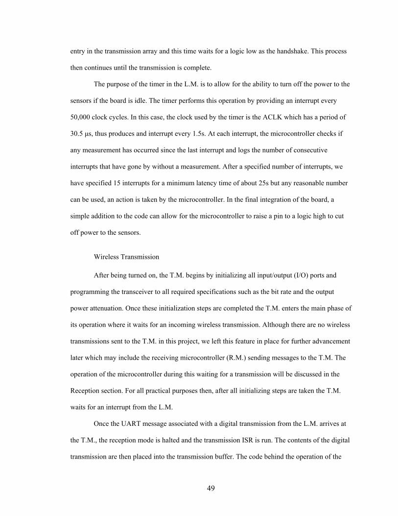
49
entry in the transmission array and this time waits for a logic low as the handshake. This process
then continues until the transmission is complete.
The purpose of the timer in the L.M. is to allow for the ability to turn off the power to the
sensors if the board is idle. The timer performs this operation by providing an interrupt every
50,000 clock cycles. In this case, the clock used by the timer is the ACLK which has a period of
30.5 μs, thus produces and interrupt every 1.5s. At each interrupt, the microcontroller checks if
any measurement has occurred since the last interrupt and logs the number of consecutive
interrupts that have gone by without a measurement. After a specified number of interrupts, we
have specified 15 interrupts for a minimum latency time of about 25s but any reasonable number
can be used, an action is taken by the microcontroller. In the final integration of the board, a
simple addition to the code can allow for the microcontroller to raise a pin to a logic high to cut
off power to the sensors.
Wireless Transmission
After being turned on, the T.M. begins by initializing all input/output (I/O) ports and
programming the transceiver to all required specifications such as the bit rate and the output
power attenuation. Once these initialization steps are completed the T.M. enters the main phase of
its operation where it waits for an incoming wireless transmission. Although there are no wireless
transmissions sent to the T.M. in this project, we left this feature in place for further advancement
later which may include the receiving microcontroller (R.M.) sending messages to the T.M. The
operation of the microcontroller during this waiting for a transmission will be discussed in the
Reception section. For all practical purposes then, after all initializing steps are taken the T.M.
waits for an interrupt from the L.M.
Once the UART message associated with a digital transmission from the L.M. arrives at
the T.M., the reception mode is halted and the transmission ISR is run. The contents of the digital
transmission are then placed into the transmission buffer. The code behind the operation of the

50
wireless transmission was written by Harsha Rao of TI which implements the basic program for
wireless transmission and reception. This code is edited to fit the needs of the project, but we
made sure to hold onto as much of the basic program as possible to preserve its reliability.
The basic program has a 17 element transmission buffer with each element containing 2
bytes or 16 bits. Of the 17 elements, 16 are used for actual data and the last entry is used as a
checksum for error detection on the receiver side. Although our project only requires the
transmission of four basic data fields and the checksum, we decided not to shorten length of the
transmission buffer since our board will not conceivably be used in particularly high speed
environments thus reduction in transmission time is not significant and the implementation with
17 elements works reliably. To make use of the 12 unused entries we filled them with the most
important item of the transmission – the length of the fish. Thus we end up sending the data a
total of 13 times. We intend then to implement a majority vote system on the receiver side that
will decide on what the length of the fish is.
Once the entire transmission buffer is filled, the Send_RF routine, written by Harsha Rao,
is run to send the data in to the transceiver. The goal of the Send_RF routine is to send the entire
transmission at 38.4Kbps, which corresponds to a bit period of 26.04 μs. The transmission
consists of a training sequence that sets the value of the sample and hold capacitor, a start bit
which is a logic high that is three times the length of a normal bit, a delay which is a logic low
that lasts twice a bit duration and the 34 bytes of data.
When programming the transceiver in the initialization steps, the T.M. selects the self-
train mode for the transceiver. In this mode, the transceiver supplies a clock signal at the desired
bit rate at the DCLK pin. This signal is used to time the duration of each data bit coming from the
T.M. The basic process is shown in Figure 16 from TI [22]
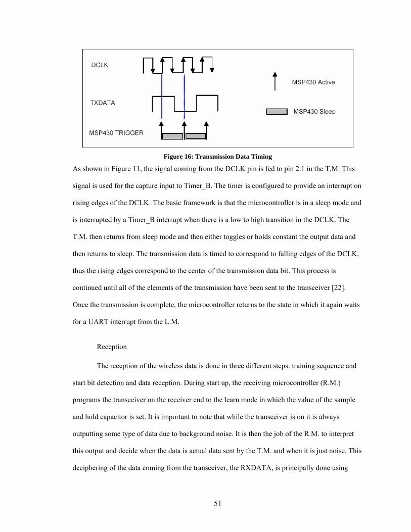
51
Figure 16: Transmission Data Timing
As shown in Figure 11, the signal coming from the DCLK pin is fed to pin 2.1 in the T.M. This
signal is used for the capture input to Timer_B. The timer is configured to provide an interrupt on
rising edges of the DCLK. The basic framework is that the microcontroller is in a sleep mode and
is interrupted by a Timer_B interrupt when there is a low to high transition in the DCLK. The
T.M. then returns from sleep mode and then either toggles or holds constant the output data and
then returns to sleep. The transmission data is timed to correspond to falling edges of the DCLK,
thus the rising edges correspond to the center of the transmission data bit. This process is
continued until all of the elements of the transmission have been sent to the transceiver [22].
Once the transmission is complete, the microcontroller returns to the state in which it again waits
for a UART interrupt from the L.M.
Reception
The reception of the wireless data is done in three different steps: training sequence and
start bit detection and data reception. During start up, the receiving microcontroller (R.M.)
programs the transceiver on the receiver end to the learn mode in which the value of the sample
and hold capacitor is set. It is important to note that while the transceiver is on it is always
outputting some type of data due to background noise. It is then the job of the R.M. to interpret
this output and decide when the data is actual data sent by the T.M. and when it is just noise. This
deciphering of the data coming from the transceiver, the RXDATA, is principally done using
52
Timer_A in the capture mode to determine the pulse width of the incoming data. As Figure 12
shows, the RXDATA pin from the transceiver is tied to the 2.0 pin in the R.M. and is used as the
input to Timer_A. Timer_A is configured to interrupt and copy the value of the count to an
appropriate register on both the rising and falling edges of the RXDATA. The values from
consecutive interrupts are then subtracted and that pulse width is then compared to the expected
pulse width of 26.04 μs to determine if it is a valid pulse [22]. It is also important to note that this
validation step is done during the training sequence of alternating highs and lows so that there
will be no consecutive highs which would not match the desired pulse width but actually would
be valid data.
Ideally the pulse width of a valid training sequence would always be 26.04 μs, but in
practice channel effects often have an impact on this pulse width. To compensate for this
possibility, the R.M. actually looks for data that falls in a range of pulse widths from 22.8 µs to
29.3 µs. The actual deciphering of the training sequence is done by the CC2_INT ISR. It looks
for 16 consecutive valid pulses to declare a valid training sequence. The reason for looking for 16
consecutive valid pulses rather than just one pulse is that given the background noise eventually
some pulse will come that falls in the acceptable range, requiring 16 such pulses reduces the
probability of an incorrect validation. After a valid training sequence is recognized, the R.M.
looks for the start bit which lasts for three times the duration of a single bit. Once the start bit is
received, the CC2_INT returns control to the Receive_RF routine for data reception [22].
Once control is transferred to the Receive_RF routine, the Timer_A capture interrupt is
disabled and the transceiver is switched from learn to hold mode. Since the transceiver is
operating in the self-train mode, the data can be read with the help of a synchronous clock output
at the DCLK terminal. Similar to the transmission, the RXDATA is timed to the falling edge of
the DCLK which would logically lead to the R.M. triggering on the rising edge of the DCLK. It
turns out that triggering on the falling edge of the DCLK actually provides better results due to
the latency between the triggering and actual latching of the R.M. The differences between

53
triggering on the rising and falling edges of the DCLK signal are shown in Figures 17 and 18
from TI [22].
Figure 17: Triggering on the Rising Edge
Figure 18: Triggering on Falling Edge
As shown in Figure 17, there is an approximately 10 μs latency period from when the R.M. is
triggered until when the RXDATA is actually latched, this leaves only about 3 μs until the next
bit period begins. Recall that channel effects often lead to a change in the bit period of the
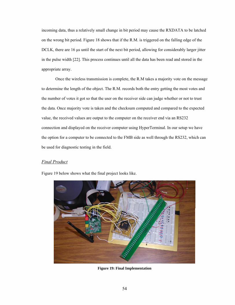
54
incoming data, thus a relatively small change in bit period may cause the RXDATA to be latched
on the wrong bit period. Figure 18 shows that if the R.M. is triggered on the falling edge of the
DCLK, there are 16 μs until the start of the next bit period, allowing for considerably larger jitter
in the pulse width [22]. This process continues until all the data has been read and stored in the
appropriate array.
Once the wireless transmission is complete, the R.M takes a majority vote on the message
to determine the length of the object. The R.M. records both the entry getting the most votes and
the number of votes it got so that the user on the receiver side can judge whether or not to trust
the data. Once majority vote is taken and the checksum computed and compared to the expected
value, the received values are output to the computer on the receiver end via an RS232
connection and displayed on the receiver computer using HyperTerminal. In our setup we have
the option for a computer to be connected to the FMB side as well through the RS232, which can
be used for diagnostic testing in the field.
Final Product
Figure 19 below shows what the final project looks like.
Figure 19: Final Implementation
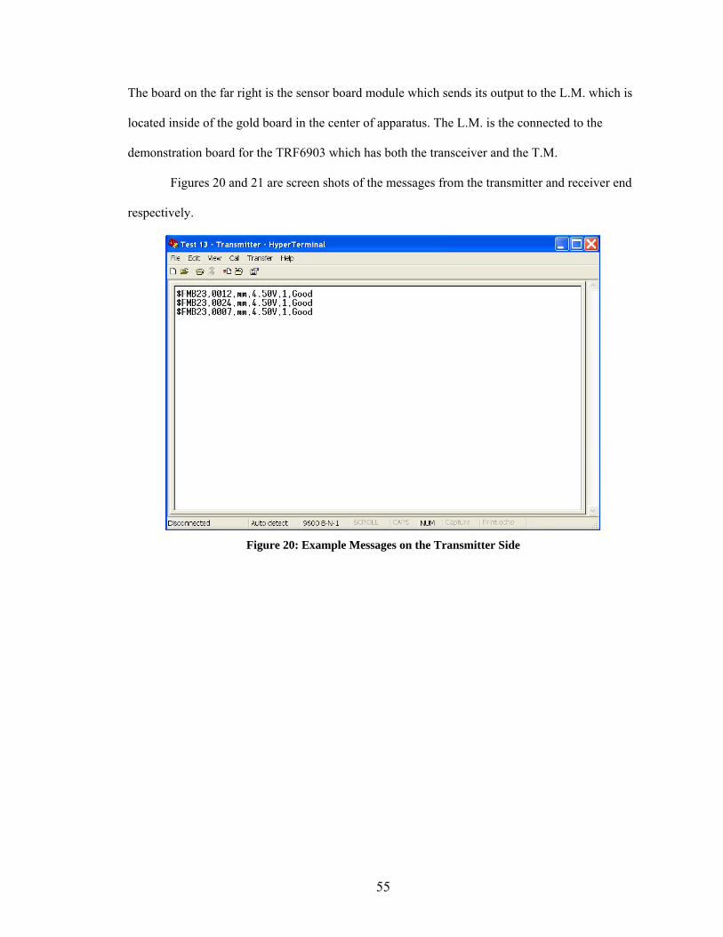
55
The board on the far right is the sensor board module which sends its output to the L.M. which is
located inside of the gold board in the center of apparatus. The L.M. is the connected to the
demonstration board for the TRF6903 which has both the transceiver and the T.M.
Figures 20 and 21 are screen shots of the messages from the transmitter and receiver end
respectively.
Figure 20: Example Messages on the Transmitter Side

56
Figure 21: Corresponding Messages on the Receiver Side
The first field in the display is the board number, as an example we have used ‘$FMB23’, but this
can easily be changed for each board by a simple edit in the code. Next is the length of the object
followed by the measurement units and the supply voltage. On the transmitter side the next field
is the status of the board, but the message on the receiver has two additional fields. The first of
these additional fields is the number of votes the length displayed got, 13 being the maximum,
and the next field indicates whether the checksum was correct, i.e. 1 for a correct checksum and 0
for an incorrect checksum.
Device Testing
After designing and implementing the system, the next step was to test it to understand how it
performed in a variety of circumstances. The principal metric used to measure the performance in
each of the circumstances in was the packet error rate. In most of the tests an incorrect
transmission is defined as the situation in which the checksums do not match up, however, in
some tests each entry is checked for errors.
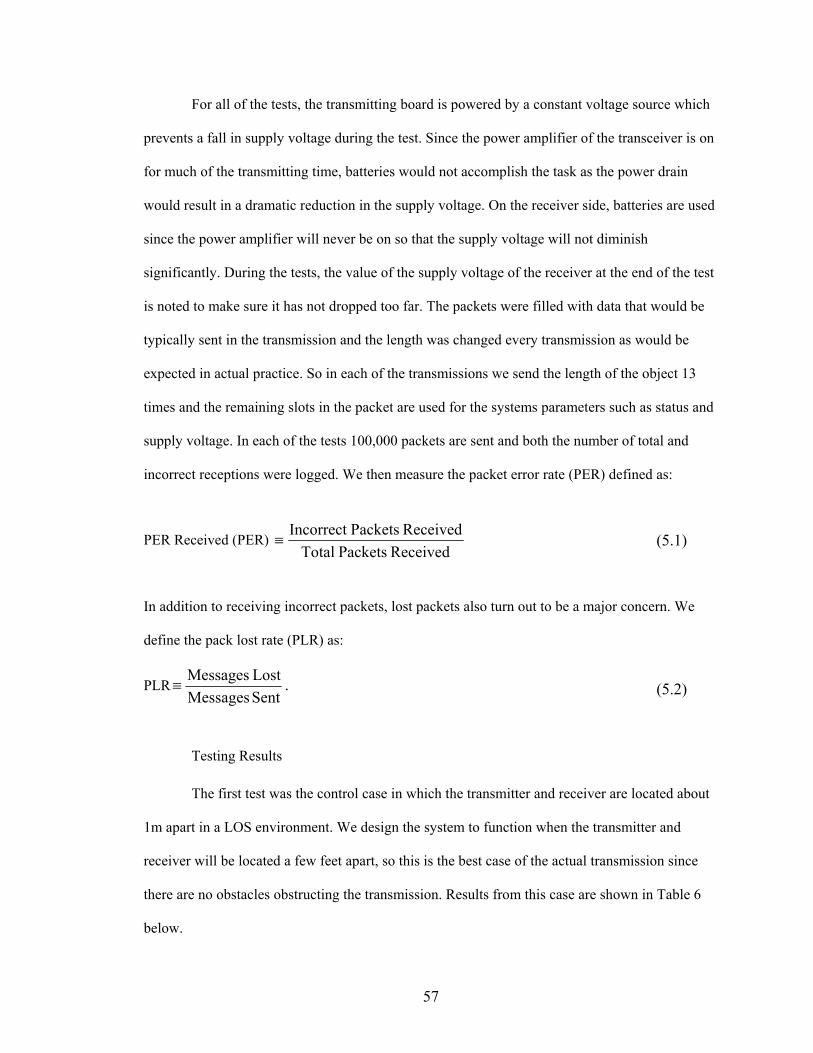
57
For all of the tests, the transmitting board is powered by a constant voltage source which
prevents a fall in supply voltage during the test. Since the power amplifier of the transceiver is on
for much of the transmitting time, batteries would not accomplish the task as the power drain
would result in a dramatic reduction in the supply voltage. On the receiver side, batteries are used
since the power amplifier will never be on so that the supply voltage will not diminish
significantly. During the tests, the value of the supply voltage of the receiver at the end of the test
is noted to make sure it has not dropped too far. The packets were filled with data that would be
typically sent in the transmission and the length was changed every transmission as would be
expected in actual practice. So in each of the transmissions we send the length of the object 13
times and the remaining slots in the packet are used for the systems parameters such as status and
supply voltage. In each of the tests 100,000 packets are sent and both the number of total and
incorrect receptions were logged. We then measure the packet error rate (PER) defined as:
PER Received (PER) ReceivedPacketsTotal
ReceivedPacketsIncorrect ≡ (5.1)
In addition to receiving incorrect packets, lost packets also turn out to be a major concern. We
define the pack lost rate (PLR) as:
PLRSent Messages LostMessages
≡ . (5.2)
Testing Results
The first test was the control case in which the transmitter and receiver are located about
1m apart in a LOS environment. We design the system to function when the transmitter and
receiver will be located a few feet apart, so this is the best case of the actual transmission since
there are no obstacles obstructing the transmission. Results from this case are shown in Table 6
below.
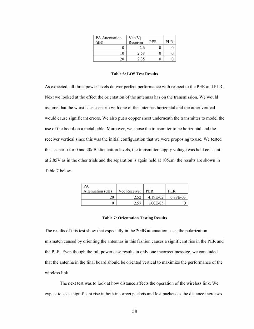
58
PA Attenuation (dB)
Vcc(V) Receiver PER PLR
0 2.6 0 0 10 2.58 0 0 20 2.35 0 0
Table 6: LOS Test Results
As expected, all three power levels deliver perfect performance with respect to the PER and PLR.
Next we looked at the effect the orientation of the antennas has on the transmission. We would
assume that the worst case scenario with one of the antennas horizontal and the other vertical
would cause significant errors. We also put a copper sheet underneath the transmitter to model the
use of the board on a metal table. Moreover, we chose the transmitter to be horizontal and the
receiver vertical since this was the initial configuration that we were proposing to use. We tested
this scenario for 0 and 20dB attenuation levels, the transmitter supply voltage was held constant
at 2.85V as in the other trials and the separation is again held at 105cm, the results are shown in
Table 7 below.
PA Attenuation (dB) Vcc Receiver PER PLR
20 2.52 4.19E-02 6.98E-03 0 2.57 1.00E-05 0
Table 7: Orientation Testing Results
The results of this test show that especially in the 20dB attenuation case, the polarization
mismatch caused by orienting the antennas in this fashion causes a significant rise in the PER and
the PLR. Even though the full power case results in only one incorrect message, we concluded
that the antenna in the final board should be oriented vertical to maximize the performance of the
wireless link.
The next test was to look at how distance affects the operation of the wireless link. We
expect to see a significant rise in both incorrect packets and lost packets as the distance increases
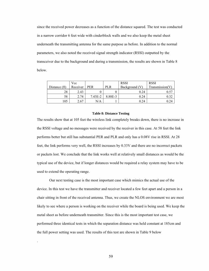
59
since the received power decreases as a function of the distance squared. The test was conducted
in a narrow corridor 6 feet wide with cinderblock walls and we also keep the metal sheet
underneath the transmitting antenna for the same purpose as before. In addition to the normal
parameters, we also noted the received signal strength indicator (RSSI) outputted by the
transceiver due to the background and during a transmission, the results are shown in Table 8
below.
Distance (ft) Vcc Receiver PER PLR
RSSI Background (V)
RSSI Transmission(V)
28 2.43 0 0 0.24 0.57 58 2.74 7.43E-2 8.88E-3 0.24 0.32
105 2.67 N/A 1 0.24 0.24
Table 8: Distance Testing
The results show that at 105 feet the wireless link completely breaks down, there is no increase in
the RSSI voltage and no messages were received by the receiver in this case. At 58 feet the link
performs better but still has substantial PER and PLR and only has a 0.08V rise in RSSI. At 28
feet, the link performs very well, the RSSI increases by 0.33V and there are no incorrect packets
or packets lost. We conclude that the link works well at relatively small distances as would be the
typical use of the device, but if longer distances would be required a relay system may have to be
used to extend the operating range.
Our next testing case is the most important case which mimics the actual use of the
device. In this test we have the transmitter and receiver located a few feet apart and a person in a
chair sitting in front of the received antenna. Thus, we create the NLOS environment we are most
likely to see where a person is working on the receiver while the board is being used. We keep the
metal sheet as before underneath transmitter. Since this is the most important test case, we
performed three identical tests in which the separation distance was held constant at 185cm and
the full power setting was used. The results of this test are shown in Table 9 below
.

60
Test Vcc Receiver (V) PER PLR 1 2.49 0 0 2 2.44 0 0 3 2.42 3.20E-04 4.50E-04
Table 9: Principal NLOS Case
The results show that the device satisfies the goal of operating in an NLOS environment typical to
what the device may be placed in. In the first two testes there were no errors and in the last case
there were a small number of errors and lost packets.
Majority Vote Analysis
After establishing that the link satisfies the goals, we next looked at the effect the
majority vote has on the transmission of length of the object. Since we were checking the value of
a particular field in the packet, we had to keep the values sent constant so that when the check
was done on the receiver end it would know what to look for. Moreover, we also sought to induce
errors in this test so we used 20dB and 10dB attenuation levels. For this test we recorded the
length error rate (LER) and the corrected length error rate (CLER), defined as:
LER ReceivedMessages ErrorsLength
≡ and (5.3)
CLER ReceivedMessages
sCorrectionMajority - ErrorsLength≡ . (5.4)
The majority vote is only considered valid for times when the result gets at least 7 votes. The
results of this test are shown in Table 10 below.
PA Attenuation (dB) LER CLER PER Improvement
20 5.91E-3 2.89E-3 7.69E-03 51% 20 3.00E-5 0 3.00E-05 100% 10 2.08E-3 1.25E-3 2.81E-03 40% 10 2.29E-3 1.45E-3 3.06E-03 36%
Table 10: Majority Vote Improvement
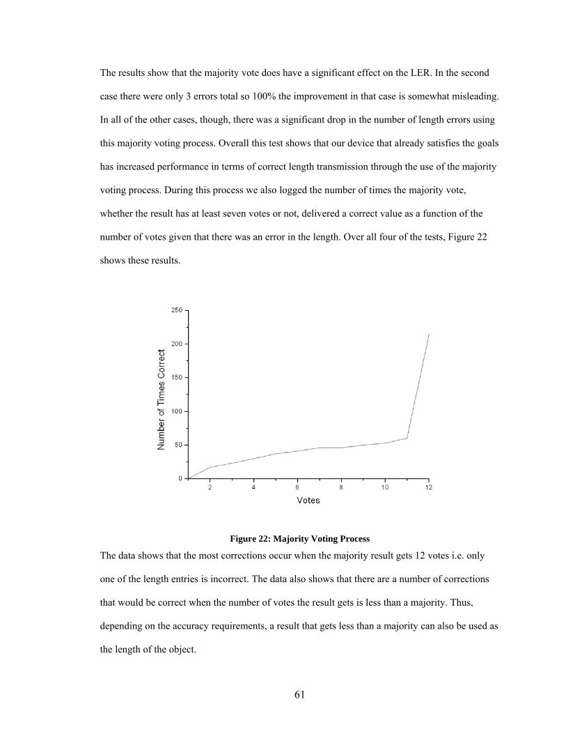
61
The results show that the majority vote does have a significant effect on the LER. In the second
case there were only 3 errors total so 100% the improvement in that case is somewhat misleading.
In all of the other cases, though, there was a significant drop in the number of length errors using
this majority voting process. Overall this test shows that our device that already satisfies the goals
has increased performance in terms of correct length transmission through the use of the majority
voting process. During this process we also logged the number of times the majority vote,
whether the result has at least seven votes or not, delivered a correct value as a function of the
number of votes given that there was an error in the length. Over all four of the tests, Figure 22
shows these results.
Figure 22: Majority Voting Process
The data shows that the most corrections occur when the majority result gets 12 votes i.e. only
one of the length entries is incorrect. The data also shows that there are a number of corrections
that would be correct when the number of votes the result gets is less than a majority. Thus,
depending on the accuracy requirements, a result that gets less than a majority can also be used as
the length of the object.

62
Overall, throughout the various tests we have shown that the wireless link that will be
used in the final board works sufficiently well in a typical NLOS environment. We also have seen
that the orientation of the two antennas plays a significant role in performance and that the device
works well at small distances but performance drops of steeply for larger distances. Finally we
showed that the majority voting process does have a positive impact on the correct reception of
the length of the object.

63
CHAPTER 6: CONCLUDING REMARKS
Future Work
Through the course of this project we have succeeded in designing and implementing the
basic technology needed for a wireless FMB that has 1mm accuracy. What remains is to package
this technology effectively and then use that final packaging in the calibration procedure. The
calibration cannot be done until the material and thickness of the stylus and protective packaging
have been decided on since they severely impact the TEAG.
Aside from the final packaging, there are improvements that can be made in the wireless
technology. We have left open the possibility of the receiver sending data to the FMB, so that
with minimal additions in the code of the receiver the receiver can query the FMB for its status,
ask for a repeat transmission in the case that the majority vote returns a length that does not get at
least seven votes and acknowledge the reception of a transmission. Moreover, the majority voting
concept can be improved upon greatly by using the myriad of coding techniques available. Since
we have allocated 208 bits to be used for the transmission of the length of the fish, this gives great
flexibility in choosing a coding scheme that can maximize the performance of the system. Lastly,
to deal with lost packet, the T.M. can use the timer to wait a predetermined amount of time for an
acknowledgement from the receiver, once this time has elapsed with no acknowledgement, the
T.M. would then re-transmit the data.
Conclusion
In conclusion, through the course of this project we have designed, implemented and
tested the basic technology needed to create a FMB that can take electronic measurements and
send them wirelessly to a receiver. We accomplished our goal of designing a wireless link that
can operate in conditions similar to what FMB operators often encounter and designed the system
out of COTS available technology. We also implemented a majority voting process that has a

64
positive impact on the length error rate. Moreover, we also designed a scheme in which only
calibration is necessary for 1mm accuracy to be achieved. We left open the possibility for
improvements in the wireless technology by allocating 208 bits to be used to code the length of
the fish and allowing the FMB to receive transmissions from the receiver.

65
APPENDIX A: LENGTH MEASUREMENT
What follows is the code necessary for the length measuring microcontroller, the files included are:
1. Length_Measure.c 2. Program_Reg.c 3. SetDCO.s43 4. trf6903_Registers.s43 5. WirelessUART_RF.s43
Of these programs, we wrote Length_Measure.c with parts of it from trf6903_WirelessUART.c written by Harsha Rao of TI, the other files are completely written by Harsha Rao as a part of the “Single-Channel Firmware” which can be found at [33].

66
// Length_Measure.c /** include files **/ #include "msp430x44x.h" #include "in430.h" #include "stdio.h" #include "rf_reg.h" #include "Ctype.h" #include "intrinsics.h" #define GIE (0x0008) #define CPUOFF (0x0010) /** local definitions **/ //TRF6903 control signals #define TRF_STROBE 0x2 #define TRF_DATA 1 #define TRF_MODE 0x80 #define TRF_CLK 0x40 #define TRF_STANDBY 0x20 #define TRF_LH 0x10 #define tx 0x4 //; P2.2 TXDATA transmit data to the TRF6901 #define rx 0x8 //; P1.3 RXDATA receive data from the TRF6901 #define TRF_LOCKDET 0x40 // P2.6 USED FOR LOCK DET #define TRF_DCLK 0x2 // P2.1 USED FOR DCLK #define TRF_RXFLAG 0x8 // P2.3 USED FOR RXFLAG #define LEDALL 0xf0 // Port definitions of Freq Select pins according #define FSEL4 0x8 #define FSEL3 0x4 #define FSEL2 0x2 #define FSEL1 0x1 #define MAXWORD 17 //size in word #define MAXBYTE 32 //size in byte #define ACK_CODE 0x6F6B // OK in ascii #define SAMPLEPERIOD 0x7800; #define XTAL_OFFSET 0 #define rF_REC_FULL 0x0001 /* RF RX buffer is full - send data to PC */ #define rS232_FULL 0x0002 /* RS232 Buf is full - read for TRF6901 to send */ #define rF_ACK_SEND 0x0004 /* RF Acknowledge is to be sent */ #define rF_ACK_WAIT 0x0008 /* RF Acknowledge is to be received */ #define RCVD 0x0010 #define RX_DLY_CNT 0x0020 // Defines the Delay from Start Bit to Data @01010h #define TS_PULSES 0x0028 // Number of pulses in the training sequence @01014h #define Num_of_Results 8 /** external functions **/

67
extern void Set_Clk(void); extern void Set_DCO(int); extern void program_TRF69(unsigned int, unsigned int); //trf6903.s43 extern void receive_RF(unsigned char, unsigned int *); extern void send_RF(unsigned int,unsigned int*); extern void rs232_link_send(unsigned int,unsigned int*); extern void configure_trf6903(void); extern void InitTRF6903(void); /** external data **/ extern struct TRF_REG trf6903; extern int PreAmbleSize; /** internal functions **/ /** public data **/ int f_sel; int opstate; unsigned int DR_DLY_CNT = 0x003F; unsigned int DR_DLY_CNT2; unsigned int DR_DLY_CNT3; unsigned int PULSE_WIDTH_TOL; unsigned int START_WIDTH_TOL; /* k1, m1 and j1 are global variables used in UART RX ISR*/ int k1=1; int m1=0; int j1=MAXBYTE; //Conversion Variables unsigned int results[42]; float volts[42]; float volts_min[32]; float min_volt; int min_array_counter = 0; int counter1; //upper level MUX select lines int counter2; //lower level MUX select lines int n; int k; float smallest; float dummy; int second; float final_location; unsigned int transmit[MAXWORD - 1] = 0; //What is communicated to the transmitter int length; int location; int sent = 0; int index;

68
int measurement_made = 0; // Track whether a measurement has been made for Timer purposes int interrupt_count = 0; // Tracks the number of interrupts int found = 0; int num_made = 0; int number_of_measurements[32]; /** private data **/ /** public functions **/ void InitIo(void); void volt_conversion(); void status(void); /** private functions **/ struct RF_XMIT_PACKET int packetsize; unsigned int xmit[MAXWORD]; unsigned int rcv[MAXWORD]; unsigned int rs232buf[MAXWORD]; unsigned int chk[1]; // stores checksum generated at the receiver for the received data buf; unsigned int Btime; unsigned int Btime1_5; void main(void) DR_DLY_CNT2 = DR_DLY_CNT -12 ; DR_DLY_CNT3 = DR_DLY_CNT2 * 3 ; PULSE_WIDTH_TOL = 0x18; START_WIDTH_TOL = PULSE_WIDTH_TOL * 3; WDTCTL = WDTPW+WDTHOLD; // Stop watchdog timer InitIo(); // Set Digital Ports P1DIR = 255; P3SEL = 0; P3DIR = 255; P3OUT = 0; P6SEL = 0x0F; // Enable A/D channel inputs ADC12CTL0 = ADC12ON+MSC+SHT0_1+REFON+REF2_5V; // ADC12 on, trigger next conversion as soon as previous ends // Set Reference to 2.5V ADC12CTL1 = SHP+CONSEQ_2+ADC12SSEL_2; // Use sampling timer, repeated single channel, use Master Clock ADC12MCTL0 = SREF_1+INCH_0; // ref+=AVcc, channel = A0 ADC12IE = 0x01; // Enable Interrupt from A0
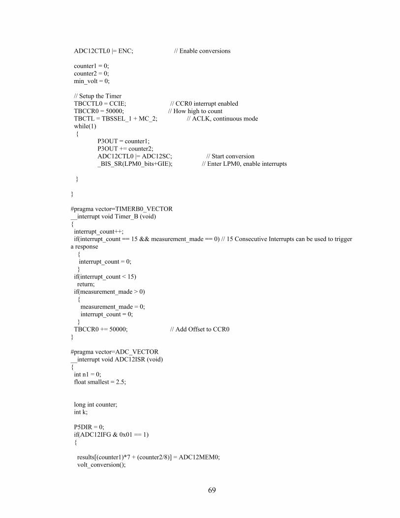
69
ADC12CTL0 |= ENC; // Enable conversions counter1 = 0; counter2 = 0; min_volt = 0; // Setup the Timer TBCCTL0 = CCIE; // CCR0 interrupt enabled TBCCR0 = 50000; // How high to count TBCTL = TBSSEL_1 + MC_2; // ACLK, continuous mode while(1) P3OUT = counter1; P3OUT += counter2; ADC12CTL0 |= ADC12SC; // Start conversion _BIS_SR(LPM0_bits+GIE); // Enter LPM0, enable interrupts #pragma vector=TIMERB0_VECTOR __interrupt void Timer_B (void) interrupt_count++; if(interrupt_count == 15 && measurement_made == 0) // 15 Consecutive Interrupts can be used to trigger a response interrupt_count = 0; if(interrupt_count < 15) return; if(measurement_made > 0) measurement_made = 0; interrupt_count = 0; TBCCR0 += 50000; // Add Offset to CCR0 #pragma vector=ADC_VECTOR __interrupt void ADC12ISR (void) int n1 = 0; float smallest = 2.5; long int counter; int k; P5DIR = 0; if(ADC12IFG & 0x01 == 1) results[(counter1)*7 + (counter2/8)] = ADC12MEM0; volt_conversion();
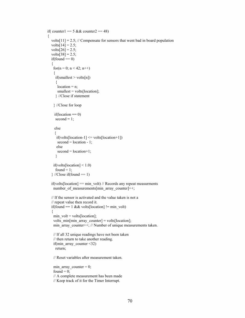
70
if( counter1 == 5 && counter2 == 48) volts[11] = 2.5; // Compensate for sensors that went bad in board population volts[14] = 2.5; volts[26] = 2.5; volts[38] = 2.5; if(found == 0) for(n = 0; n < 42; n++) if(smallest > volts[n]) location = n; smallest = volts[location]; //Close if statement //Close for loop if(location == 0) second = 1; else if(volts[location-1] <= volts[location+1]) second = location - 1; else second = location+1; if(volts[location] < 1.0) found = 1; //Close if(found == 1) if(volts[location] == min_volt) // Records any repeat measurments number_of_measurements[min_array_counter]++; // If the sensor is activated and the value taken is not a // repeat value then record it. if(found == 1 && volts[location] != min_volt) min_volt = volts[location]; volts_min[min_array_counter] = volts[location]; min_array_counter++; // Number of unique measurements taken. // If all 32 unique readings have not been taken // then return to take another reading. if(min_array_counter <32) return; // Reset variables after measurement taken. min_array_counter = 0; found = 0; // A complete measurement has been made // Keep track of it for the Timer Interrupt.
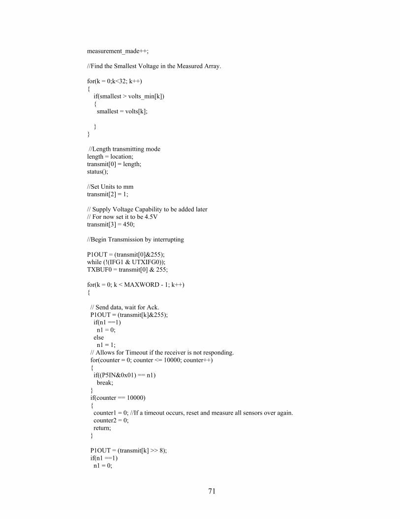
71
measurement_made++; //Find the Smallest Voltage in the Measured Array. for(k = 0;k<32; k++) if(smallest > volts_min[k]) smallest = volts[k]; //Length transmitting mode length = location; transmit[0] = length; status(); //Set Units to mm transmit[2] = 1; // Supply Voltage Capability to be added later // For now set it to be 4.5V transmit[3] = 450; //Begin Transmission by interrupting P1OUT = (transmit[0]&255); while (!(IFG1 & UTXIFG0)); TXBUF0 = transmit[0] & 255; for(k = 0; k < MAXWORD - 1; k++) // Send data, wait for Ack. P1OUT = (transmit[k]&255); if(n1 ==1) n1 = 0; else n1 = 1; // Allows for Timeout if the receiver is not responding. for(counter = 0; counter <= 10000; counter++) if((P5IN&0x01) == n1) break; if(counter == 10000) counter1 = 0; //If a timeout occurs, reset and measure all sensors over again. counter2 = 0; return; P1OUT = (transmit[k] >> 8); if(n1 ==1) n1 = 0;
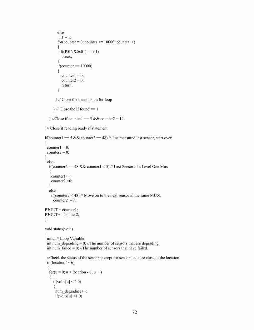
72
else n1 = 1; for(counter = 0; counter <= 10000; counter++) if((P5IN&0x01) == n1) break; if(counter == 10000) counter1 = 0; counter2 = 0; return; // Close the transmision for loop // Close the if found == 1 //Close if counter1 == 5 && counter2 = 14 // Close if reading ready if statement if(counter1 == 5 && counter2 == 48) // Just measured last sensor, start over counter1 = 0; counter2 = 0; else if(counter2 == 48 && counter1 < 5) // Last Sensor of a Level One Mux counter1++; counter2 =0; else if(counter2 < 48) // Move on to the next sensor in the same MUX. counter2+=8; P3OUT = counter1; P3OUT+= counter2; void status(void) int u; // Loop Variable int num_degrading = 0; //The number of sensors that are degrading int num_failed = 0; //The number of sensors that have failed. //Check the status of the sensors except for sensors that are close to the location if (location >=6) for(u = 0; u < location - 6; u++) if(volts[u] < 2.0) num_degrading++; if(volts[u] <1.0)

73
num_failed++; num_degrading--; // End of for loop //Close if statement if (location <38) for(u = location +4; u<42; u++) if(volts[u] < 2.0) num_degrading++; if(volts[u] <1.0) num_failed++; num_degrading--; // End of for loop //Close if statement if(num_degrading == 0 && num_failed ==0) transmit[1] = 1; else if(num_degrading > 0 && num_failed ==0) transmit[1] = 2; else if(num_failed >0) transmit[1] = 3; void volt_conversion() volts[(counter1)*7 + (counter2/8)] = (((float)results[(counter1)*7 + (counter2/8)])/4095)*2.50; void InitIo(void) opstate|=0x00; // initilalize opstate P2DIR|= tx; // TXDATA is set to output direction P2SEL=0x33; //UART for P2.4 and P2.5, TimerA,TimerB capture for RXDATA and DCLK Set_DCO(30000); //set dco for = 2.4576 MHz //initialize UART port. Default Baud =38.4K UTCTL0=0x20; // Select SMCLk as the source for UART clock URCTL0=0x8; UBR00 = 0; //9600bps UBR10 = 0x01;

74
UMCTL0=0x0; UCTL0=0x11; UCTL0&=0xfe; // at first disable UART ME1|=URXE0+UTXE0; //enable both transmitter and receiver
75
// Program_Reg.c /************************************************************************************** RF_reg.c AUTHOR: Harsha Rao ***************************************************************************************/ /**************************** Programming the TRF6903 ************************************************** TX = Mode_0: A Word is programmed for FSK transmission (Mode bit =1) RX = Mode_1: B Word is programmed for FSK receive (Mode bit =0) ;*******************************************************************************************************/ #include "rf_reg.h" #include "msp430x44x.h" #include "in430.h" #include "stdio.h" #include "f_6903.h" #define ENABLE_DCLK 1 extern int f_sel,fsel_update; extern unsigned int DR_DLY_CNT; struct TRF_REG trf6903; extern void program_TRF69(unsigned int, unsigned int); //trf6903.s43 void program_TRF6903_word(unsigned long ); void configure_trf6903(void); void InitTRF6903(void); int PreAmbleSize; void InitTRF6903(void) trf6903.a.bit.BND = 2; //select 900Mhz trf6903.a.bit.CP_Acc=0; trf6903.a.bit.PI = 0; trf6903.a.bit.TX_RX0 = 1; //low on mode means transmit trf6903.a.bit.PA0=0; trf6903.a.bit.B_DIV_M0 = 68; //set to 902 trf6903.a.bit.A_DIV_M0 = 27 ; trf6903.a.bit.ADDR =0; //0x2854A2 trf6903.b.bit.DET_EN = 1; //start off disabled trf6903.b.bit.DET_THRESH = 0; //2.2V trf6903.b.bit.PARXED = 1; trf6903.b.bit.FSK_OOK=1; trf6903.b.bit.TX_RX1=0; //receive when mode input =high trf6903.b.bit.PA1=0; trf6903.b.bit.B_DIV_M1 = 68;
76
trf6903.b.bit.A_DIV_M1 = 1; trf6903.b.bit.ADDR=1; //0x685599 trf6903.c.bit.reserved = 0; //start off disabled trf6903.c.bit.REF_DIV_COEF = 48; trf6903.c.bit.ADDR = 2; trf6903.d.bit.reserved1 = 0; //start off disabled trf6903.d.bit.OOKXS = 0; //2.2V trf6903.d.bit.DEM_TUNE = 7; //6 trf6903.d.bit.PFD_reset=1; trf6903.d.bit.XTAL_Tune=6; //receive when mode input =high trf6903.d.bit.RXS=1; trf6903.d.bit.reserved2 = 0; trf6903.d.bit.ADDR = 3; //0XC0E000 trf6903.e.bit.reserved1 = 1; // trf6903.e.bit.PAI = 2; //Nominal trf6903.e.bit.TCOUNT = 5; //Minimum training = 4 times the value //trf6903.e.bit.TCOUNT =30 ; //Minimum training = 4 times the value trf6903.e.bit.TWO=0; //receive when mode input =high //#ifdef ENABLE_DCLK trf6903.e.bit.TXM = 1; //use DCLK to send data //#else // trf6903.e.bit.TXM = 0; //use RAW //#endif trf6903.e.bit.RXM = 3; if (DR_DLY_CNT == 0x007F) trf6903.e.bit.D3 = 0 ; trf6903.e.bit.D2 = 3 ; // 19.2 k trf6903.e.bit.D1 = 3 ; if (DR_DLY_CNT == 0x003F) trf6903.e.bit.D3 = 0 ; trf6903.e.bit.D2 = 2 ; // 38.4 k trf6903.e.bit.D1 = 3 ; if (DR_DLY_CNT == 0x002F) trf6903.e.bit.D3 = 0 ; trf6903.e.bit.D2 = 2 ; // 51.2 k trf6903.e.bit.D1 = 2 ; trf6903.e.bit.ADDR = 2; PreAmbleSize = trf6903.e.bit.TCOUNT; PreAmbleSize =(PreAmbleSize*4) + 100; void configure_trf6903(void) int pointer; P4OUT&=0xfe; //start with 0 on data

77
pointer=(int)f_sel; trf6903.a.bit.B_DIV_M0=MAIN_B_T[pointer]; trf6903.a.bit.A_DIV_M0=MAIN_A_T[pointer]; program_TRF6903_word(trf6903.a.all); trf6903.b.bit.B_DIV_M1=MAIN_B_R[pointer]; trf6903.b.bit.A_DIV_M1=MAIN_A_R[pointer]; program_TRF6903_word(trf6903.b.all); program_TRF6903_word(trf6903.c.all); trf6903.d.bit.XTAL_Tune = XTAL_OFFSET; program_TRF6903_word(trf6903.d.all); program_TRF6903_word(trf6903.e.all); void program_TRF6903_word(unsigned long control) unsigned int high,low; high = (unsigned int)(control>>16); low =(unsigned int)control; program_TRF69(high,low);
78
; set_dco.s43 ;This module sets the clock. ;================================================================================ #include "msp430x44x.h" #define Count1 R8 #define Count2 R9 MODULE Set_DCO PUBLIC Set_DCO RSEG CODE ;Adjust DCO Routine Set_DCO MOV.B #(75-1),&SCFQCTL_ MOV.B #FN_3,&SCFI0_ ;MOV.B #030h,&FLL_CTL0_ ;10pf load MOV.B #010h,&FLL_CTL0_ ;6pf load Set_DCO1 BIC.B #OFIFG,&IFG1_ NOT_COOKED MOV R12,Count1 ;20 is the wait time WAIT? DEC Count1 //JNZ WAIT? //BIT.B #OFIFG, &IFG1_ ;test oscillator fault flag //JNZ Set_DCO ; Repeat until test flag remains reset MOV #WDTPW+WDTHOLD,&WDTCTL ; if start detected, WDT set to timeout every 52uS RET ENDMOD MODULE ReStart PUBLIC ReStart RSEG CODE ReStart MOV #0fffeh,R5 BR @R5 RET ENDMOD ; END // The Set_Clk routine is never called since XT2 OSC is not used on the demo board
79
MODULE Set_Clk PUBLIC Set_Clk RSEG CODE Set_Clk BIC.B #XT2OFF, &FLL_CTL1_ ; Turn on the High XT2 Xtal TST_OF BIC.B #OFIFG,&IFG1_ MOV #20,Count1 ;20 is the wait time LOOP DEC Count1 JNZ LOOP BIT.B #OFIFG, &IFG1_ ;test oscillator fault flag JNZ TST_OF ; Repeat until test flag remains reset MOV.B #SELM_XT2+SELS,&FLL_CTL1_ ; select the proper clock RET ENDMOD END

80
;trf6903_Registers.s43 /**************************** program_TRF69 ********************************************************** ; purpose: ; programs a word to A, B, C or D word register of the TRF6901 ; gets the settings from the calling routine in R6 and R7 ; ;*******************************************************************************************************/ #include "msp430x44x.h" #include "std_f43x.asm" #define Count1 R8 #define Count2 R9 #define counter R10 ; universal counter NAME TRF6901 RSEG CODE(1) PUBLIC program_TRF69 EXTERN ?CL430_1_23_L08 RSEG CODE program_TRF69 init_high_byte DINT PUSH R10 PUSH R9 PUSH R8 PUSH R7 PUSH R6 PUSH R5 PUSH R4 MOV R12,word_h ;mov data to appropriate register MOV R14,word_l BIC.B #strobe,&P4OUT ; reset Strobe port BIS.B #strobe,&P4DIR ; switch Strobe to output direction MOV #02h,counter ; initialize the counter for high and low byte MOV #08h,bits_r ; initialize bitcounter ; MOV word_h,word_trf MOV R6,R4 SWPB word_trf ; push the low byte to the high byte, only the ; data in the low byte is relevant JMP program_word

81
init_low_byte MOV #010h,bits_r ; initialize bitcounter ; MOV word_l,word_trf ; push the low byte to the programming buffer MOV R7,R4 program_word RLC word_trf ; push the msb of the programming buffer to carry JNC program_low program_high BIS.B #data,&P4OUT ; set data(P1.7) program_clock BIS.B #clk,&P3OUT ; generate a pulse on the clock line BIC.B #clk,&P3OUT program_next_bit DEC bits_r ; decrement bit counter JNZ program_word ; have already all bits been sent? DEC counter ; decrement counter for low byte recognition JNZ init_low_byte ; low byte is to be programmed generate_strobe BIC.B #data,&P4OUT ; reset data BIS.B #strobe,&P4OUT ; set strobe(P1.5) BIC.B #strobe,&P4OUT ; clear strobe(P1.5) BIC.B #strobe,&P4DIR ; set strobe(P1.5) to input direction POP R4 POP R5 POP R6 POP R7 POP R8 POP R9 POP R10 EINT RET ; back to calling routine program_low BIC.B #data,&P4OUT ; clear data(P1.7)

82
JMP program_clock end_program_TRF69 END
83
;WirelessUART_RF.s43 ;/**************************************************************** ; Author - Harsha Rao ;Interrupt subroutines and send and receive RF drivers ;****************************************************************/ #include "msp430x44x.h" #include "std_f43x.asm" #define rF_REC_FULL 0x0001 /* RF RX buffer is full - send data to PC */ #define rS232_FULL 0x0002 /* RS232 Buf is full - read for TRF6901 to send */ #define rF_ACK_SEND 0x0004 /* RF Acknowledge is to be sent */ #define rF_ACK_WAIT 0x0008 /* RF Acknowledge is to be received */ #define RCVD 0x0010 #define RSTAT R8 ; status of the reception #define wait_r R9 ; counter register for all waiting loops ***** #define counter R10 ; universal counter #define RX_DLY_CNT 0x0028 // Not Used in the Firmware #define TS_PULSES 0x0080 // Number of pulses in the training sequence @01014h*/ NAME radio(16) RSEG CODE(1) COMMON INTVEC(1) EXTERN time_out_count EXTERN opstate EXTERN DR_DLY_CNT EXTERN DR_DLY_CNT2 EXTERN DR_DLY_CNT3 EXTERN PULSE_WIDTH_TOL EXTERN START_WIDTH_TOL EXTERN k1 EXTERN m1 EXTERN j1 EXTERN Set_DCO EXTERN Btime EXTERN Btime1_5 PUBLIC Timer_A1 PUBLIC receive_RF PUBLIC send_RF PUBLIC rs232_link_send PUBLIC wait_lockdet EXTERN ?CL430_1_23_L08 RSEG CODE MOV #09F0h,SP

84
Timer_A1: ADD &TAIV,PC RETI RETI JMP CC2_INT ; RF reception -> every edge of ; the rx-signal RETI RETI ?back RETI ;************************************* Timer_B Interrupt routine *********** ; purpose: handle the Timer_B interrupts, and decide which dedicated routine ; should be addressed. (TB_CCR0 / RF reception and transmission) ;**************************************************************************** TimerB0 BIC #CPUOFF,0(SP) ; reactivate CPU end_TB_CCR0 RETI ;****************************** Capture Compare 2 Register ********************************************* ; used for RF-Reception ;******************************************************************************************************* CC2_INT ; used by biph_rx MOV RRFTAB(R8),PC ; conditional jump depends on RSTAT ; RSTAT = 0, detecting the Trianingsequence ; RSTAT = 1, Trainingsquence detected, waiting ; for the Start Bit ; RSTAT = 2, Start Bit detected, Data Reception RRFTAB DW RSTAT00 DW RSTAT01 DW RSTAT10 DW RSTAT11 RSTAT00 MOV &CCR2,R14 ; save Reference Capture value MOV R14,R15 ; copy Timer_A value SUB R13,R15 ; subtract the current Timer_A value from the ; old one -> Bitwidth in cycles in res_r

85
MOV R14,R13 ; current value now -> old value later test_res_r00 SUB DR_DLY_CNT2,R15 CMP PULSE_WIDTH_TOL,R15 ;4/18 is the detected signal 20-34uS long? JHS no_valid_pulse INCD R8 ; first valid pulse detected INC wake_up_counter ; count this valid pulse BIS #CCIE,&CCTL2 ; re-enable CCR2 interrupt JMP go_back no_valid_pulse CLR R8 ; no the signal doesn't fit the wakeup sequence CLR wake_up_counter ; reset the wake_up_counter, received an ; invalid pulse JMP go_back /******************************************************************************************************************************************/ RSTAT01 MOV &CCR2,R14 ; save Reference Capture value MOV R14,R15 ; copy Timer_A value SUB R13,R15 ; subtract the current Timer_A value from the ; old one -> Bitwidth in cycles in res_r MOV R14,R13 ; current value now -> old value later test_res_r01 SUB DR_DLY_CNT2,R15 CMP PULSE_WIDTH_TOL,R15 ;4/18 is the detected signal 20-34uS long? JHS no_valid_pulse INC wake_up_counter ; next valid pulse JMP go_back /*******************************************************************************************************************************************/ RSTAT10 MOV &CCR2,R14 ; save Reference Capture value MOV R14,R15 ; copy Timer_A value SUB R13,R15 ; subtract the current Timer_A value from ; the old one -> Bitwidth in cycles in res_r MOV R14,R13 ; current value now -> old value later

86
test_res_r10 SUB DR_DLY_CNT3,R15 ;CMP #038,R15 ; is the detected signal x cycles long? This is for asymmetric stuff CMP START_WIDTH_TOL,R15 JGE invalid_bit ; restart detection, this is not a valid sequence JHS no_start_int_enable INCD R8 ; go to RSTATE 2, Data Reception, Start Bit ; detected BIC #CCIE,&CCTL2 ; disable CCR2 interrupt BIC #022h,&TACTL ; stop Timer_A and disable interrupt no_start_bit INC wake_up_counter ; count the pulses of the trainings sequence, CMP #TS_PULSES,wake_up_counter ; compare the value of the counter with the JGE invalid_bit ; JMP go_back ;get ready for data collection no_start_int_enable JMP no_start_bit invalid_bit CLR R8 ; restart the detection, this is not a valid CLR wake_up_counter ; initialize the wake_up_counter go_back BIC #CPUOFF,0(SP) ; wake up! RETI /******************************************************************************************************************************************/ /* Not Used in this version of Firmware*/ /*****************************************************************************************************************************************/ RSTAT11 BIT #CAP,&CCTL2 ; if in capture mode, just found start bit JNZ R_start_edge_detected ; due to negative edge BIC.B #rx,&P2SEL ;make it into GPIO BIT.B #rx,&P2IN ;read IObit RLC data_r ; push carry into the data register BIS.B #rx,&P2SEL ;go back to module ADD &Btime,&CCR2
87
INC bits_r CMP #010h,bits_r ; receive 16 bits in row JNE end_RSTAT11_INT ;get all bits BIC #CCIE,&CCTL2 ;no more int JMP end_RSTAT11_INT R_start_edge_detected BIC #CAP,&CCTL2 ;go to compare mode ADD &Btime1_5,&CCR2 ;get ready to receive data CLR bits_r end_RSTAT11_INT ; before the interrupt request, but start BIC #CPUOFF,0(SP) ; wake up! ; subroutine RETI kill_receive BIC #CCIE,&CCTL2 ; disable CCR2 interrupt BIC #022h,&TACTL ; stop Timer_A and disable interrupt BIC #CPUOFF,0(SP) ; wake up! RETI ;*********************************** send_RF *********************************************************** ; purpose: sends data through RF channel ;******************************************************************************************************* send_RF BIC.B #URXIFG0,&IFG1 ; Clear Receive Interrupt Flag BIC.B #URXIE0,&IE1 ; Disable USART1 Receive Interrupt send_RF_acknowledge? BIT #rF_ACK_SEND,&opstate ; has an acknowledge to be send? JNZ send_RF_init data_to_transmit? BIT #rS232_FULL,&opstate ; Is there any data to send via TRF6901? JZ end_send_RF ; No, nothing to send send_RF_init DINT MOV R12,R10 MOV R12,R6 ADD R14,R10 BIC.B #mode,&P3OUT ; Mode=0 -> Send mode BIC.B #tx,&P2OUT ; TXDATA(P2.2) is reset BIS.B #stdb_trf6901,&P3OUT ; TRF6900 active, STANDBY(P3.5) is high DECD R10
88
MOV 0(R10),data_r ; first word to the send register ;This is where clock recovery happens--DCLK has to be connected to the P2.1/TB0 pin MOV #0x4910,&TBCCTL0 ; enable TBCCR0 Interrupt, Capture on Positive Edge of DCLK ; MOV #0x8910,&TBCCTL0 ;capture on negative edge MOV #0x0224,&TBCTL ; enable TIMERB and start in Continous mode EINT send_RF_training_sequence ; the entire length ca. 4ms, 154 pulses MOV #TS_PULSES, tr_counter ; initialize the training sequence counter send1_RF_toggle BIS #CPUOFF+GIE,SR ; CPU off ;------------------ Start of the trainings sequence ---------------------------------------------------- XOR.B #tx,&P2OUT ; toggle TXDATA(P2.2) DEC tr_counter ; decrement counter for the training sequence JNZ send1_RF_toggle ; JMP send1_RF_toggle ; ADD TRIGGER HERE BIC.B #l_h,&P3OUT ; END TRIGGER send_RF_long_bit BIS #CPUOFF+GIE,SR ; CPU off ;------------------ Start of the start bit ------------------------------------------------------------- BIS.B #tx,&P2OUT ; start of the long start-bit 78,12ec BIS #CPUOFF+GIE,SR ; CPU off BIC #rS232_FULL,&opstate ; the RS232 buffer is ready for reception BIS #CPUOFF+GIE,SR ; CPU off BIS #CPUOFF+GIE,SR ; CPU off ;----------------- End of the start bit ---------------------------------------------------------------- start_bit_low BIC.B #tx,&P2OUT ; reset TXDATA(P2.2) MOV DR_DLY_CNT,wait_r INC wait_r RRA wait_r ; used for DIV by 2 send_pause_dly DEC wait_r JNZ send_pause_dly send_RF_data MOV #010h,bits_r ; init bitcounter, transmit first 16 bits
89
send_RF_bit_test RLC data_r ; push the next data bit to carry JC send_RF_high send_RF_low BIC.B #tx,&P2OUT ; reset TXDATA(P2.2) BIS #CPUOFF+GIE,SR ; CPU off ;-------------------------------- Start of the Databit ------------------------------------------------- send_RF_next_word? DEC bits_r ; decrement bit counter JNZ send_RF_bit_test DECD R10 ; decrement word counter DECD R6 JZ send_RF_complete JN send_RF_reset_ackn ; all data has been transmitted MOV 0(R10),data_r JMP send_RF_data ; get next word by sending active low start bit first send_RF_high BIS.B #tx,&P2OUT ; set TXDATA(P2.2) BIS #CPUOFF+GIE,SR ; CPU off ;-------------------------------- Start of the Databit ------------------------------------------------- JMP send_RF_next_word? send_RF_reset_ackn BIC #rF_ACK_SEND,&opstate ; reset acknowledge state send_RF_complete BIS.B #0xF0,&P1OUT MOV #01000,wait_r ;retry about 10 times noyet DEC wait_r ;tried enough? JNZ noyet BIC.B #0xF0,&P1OUT BIS #CPUOFF+GIE,SR ; CPU off-accomodate TRF6901 timing BIC.B #tx,&P2OUT BIC.B #stdb_trf6901,&P3OUT ; clear STDBY(P3.5), TRF6901 standby mode end_send_RF BIC #0x0012,&TBCTL ; stop and disable TIMERB BIC #0x0010,&TBCCTL0 ; disable TBCCR0 Interrupt BIC.B #URXIFG0,&IFG1 ; Clear Receive Interrupt Flag BIS.B #URXIE0,&IE1 ; RE-Enable USART1 Receive Interrupt skip_send_RF RET ;********************************* receive_RF **********************************************************
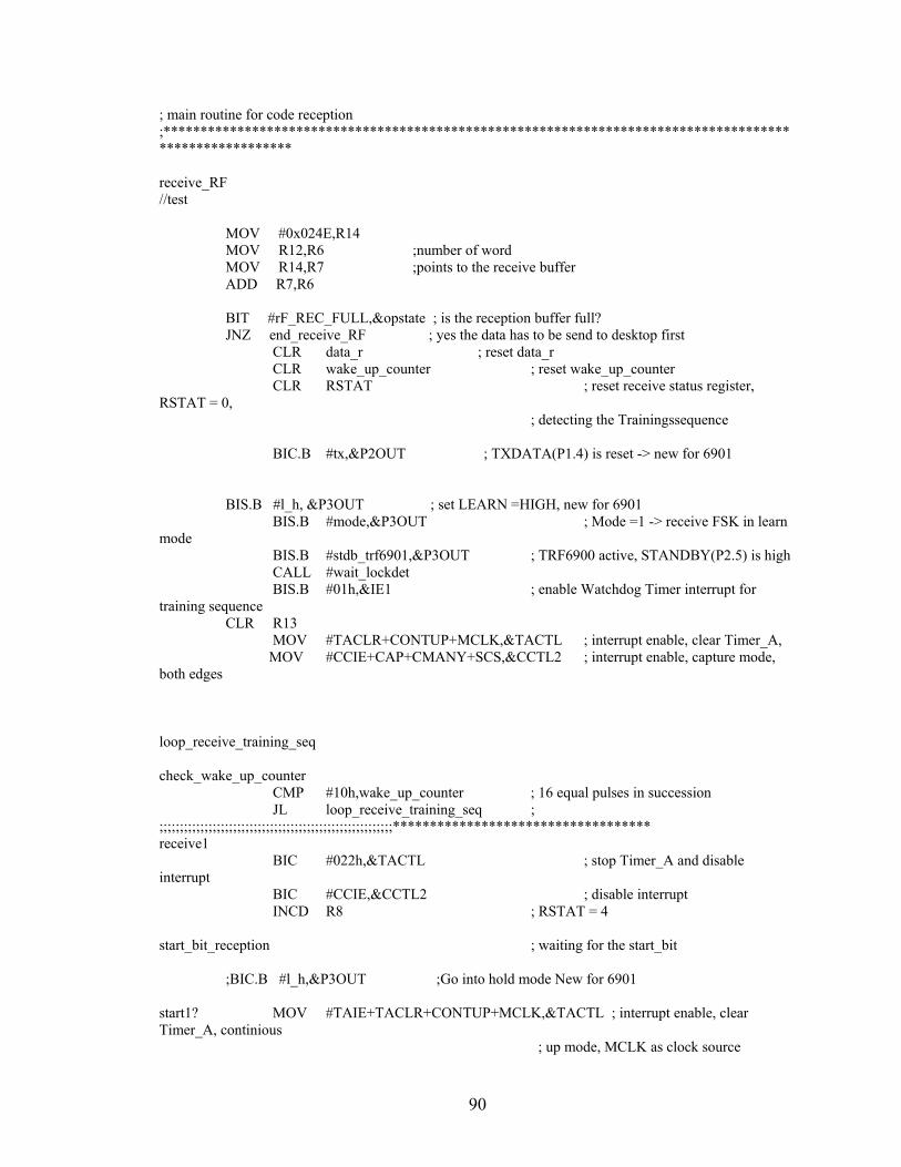
90
; main routine for code reception ;******************************************************************************************************* receive_RF //test MOV #0x024E,R14 MOV R12,R6 ;number of word MOV R14,R7 ;points to the receive buffer ADD R7,R6 BIT #rF_REC_FULL,&opstate ; is the reception buffer full? JNZ end_receive_RF ; yes the data has to be send to desktop first CLR data_r ; reset data_r CLR wake_up_counter ; reset wake_up_counter CLR RSTAT ; reset receive status register, RSTAT = 0, ; detecting the Trainingssequence BIC.B #tx,&P2OUT ; TXDATA(P1.4) is reset -> new for 6901 BIS.B #l_h, &P3OUT ; set LEARN =HIGH, new for 6901 BIS.B #mode,&P3OUT ; Mode =1 -> receive FSK in learn mode BIS.B #stdb_trf6901,&P3OUT ; TRF6900 active, STANDBY(P2.5) is high CALL #wait_lockdet BIS.B #01h,&IE1 ; enable Watchdog Timer interrupt for training sequence CLR R13 MOV #TACLR+CONTUP+MCLK,&TACTL ; interrupt enable, clear Timer_A, MOV #CCIE+CAP+CMANY+SCS,&CCTL2 ; interrupt enable, capture mode, both edges loop_receive_training_seq check_wake_up_counter CMP #10h,wake_up_counter ; 16 equal pulses in succession JL loop_receive_training_seq ; ;;;;;;;;;;;;;;;;;;;;;;;;;;;;;;;;;;;;;;;;;;;;;;;;;;;;;;;;;*********************************** receive1 BIC #022h,&TACTL ; stop Timer_A and disable interrupt BIC #CCIE,&CCTL2 ; disable interrupt INCD R8 ; RSTAT = 4 start_bit_reception ; waiting for the start_bit ;BIC.B #l_h,&P3OUT ;Go into hold mode New for 6901 start1? MOV #TAIE+TACLR+CONTUP+MCLK,&TACTL ; interrupt enable, clear Timer_A, continious ; up mode, MCLK as clock source

91
MOV #SCS+CCIE+CAP+CMANY,&CCTL2 ; interrupt enable, capture mode, both edges CLR R13 loop_start_bit CMP #04h,R8 ; has the start bit been detected? JEQ loop_start_bit ; wait for the start bit JN end_receive_RF ; the received sequence is invalid ; TEST BIC.B #l_h,&P3OUT ;----------------------------- start bit detected ------------------------------------------------------ init_data_reception ; RSTAT = 6, Start Bit detected, Data Reception send_rx_pause_dly BIC #CCIE,&CCTL2 ; disable CCR2 interrupt BIC #022h,&TACTL ; stop Timer_A and disable interrupt BIC.B #URXIE0,&IE1 ; Disable USART1 Receive Interrupt ;This is where clock recovery happens--DCLK has to be connected to the P2.1/TB0 pin ; MOV #0x4910,&TBCCTL0 ; enable TBCCR0 Interrupt, Capture on Positive Edge of DCLK MOV #0x8910,&TBCCTL0 ;capture on negative edge MOV #0x0224,&TBCTL ; enable TIMERB and start in Continous mode init_rx_bit_counter CLR bits_r word_reception_loop BIS #CPUOFF+GIE,SR ; go to sleep! BIT.B #rx,&P2IN ; is RXDATA high or low? read_data RLC data_r ; push carry into the data register INC bits_r CMP #010h,bits_r ; receive 16 bits in row JNE word_reception_loop ; haven't received 8bits yet store_data ; INV data_r ; the received data is inverted! MOV data_r,0(R7) ; store received data to RAM INCD R7 CMP R6,R7 JNE init_rx_bit_counter ; receive the next word ready_to_end NOP
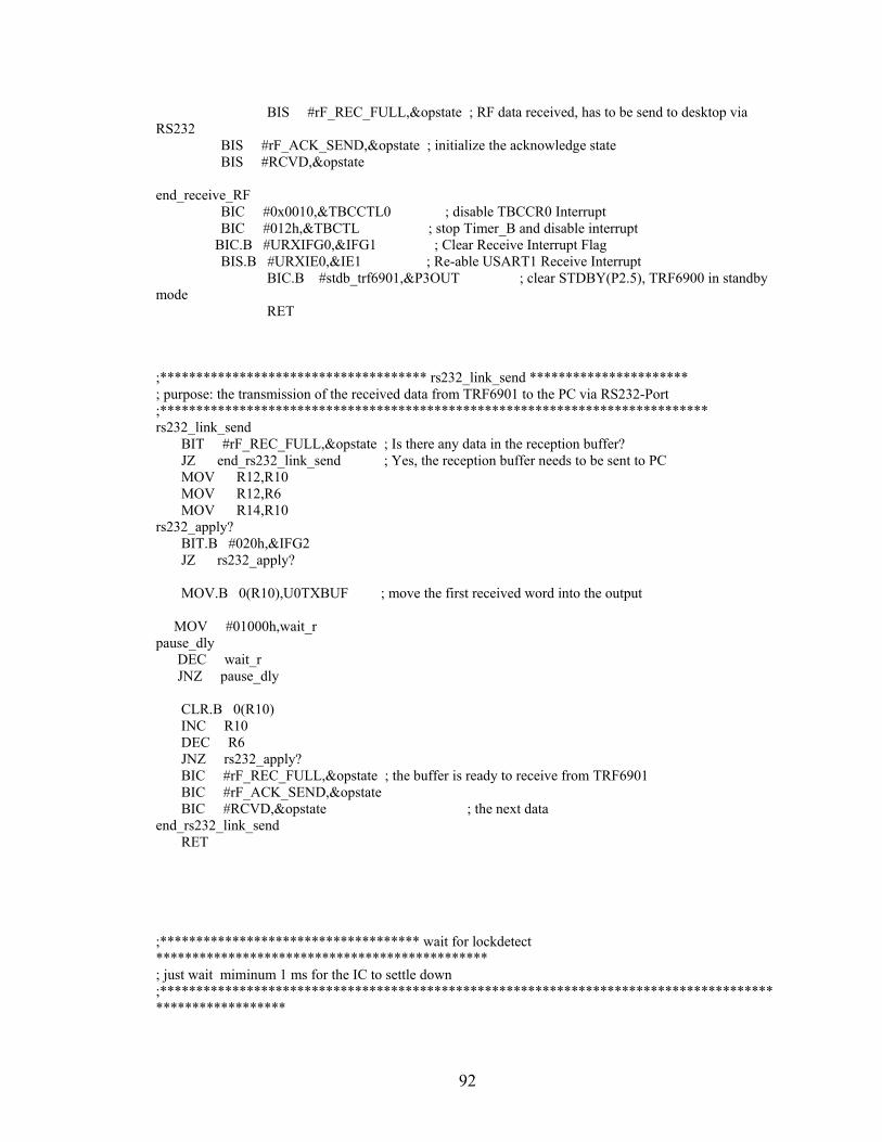
92
BIS #rF_REC_FULL,&opstate ; RF data received, has to be send to desktop via RS232 BIS #rF_ACK_SEND,&opstate ; initialize the acknowledge state BIS #RCVD,&opstate end_receive_RF BIC #0x0010,&TBCCTL0 ; disable TBCCR0 Interrupt BIC #012h,&TBCTL ; stop Timer_B and disable interrupt BIC.B #URXIFG0,&IFG1 ; Clear Receive Interrupt Flag BIS.B #URXIE0,&IE1 ; Re-able USART1 Receive Interrupt BIC.B #stdb_trf6901,&P3OUT ; clear STDBY(P2.5), TRF6900 in standby mode RET ;************************************* rs232_link_send ********************** ; purpose: the transmission of the received data from TRF6901 to the PC via RS232-Port ;**************************************************************************** rs232_link_send BIT #rF_REC_FULL,&opstate ; Is there any data in the reception buffer? JZ end_rs232_link_send ; Yes, the reception buffer needs to be sent to PC MOV R12,R10 MOV R12,R6 MOV R14,R10 rs232_apply? BIT.B #020h,&IFG2 JZ rs232_apply? MOV.B 0(R10),U0TXBUF ; move the first received word into the output MOV #01000h,wait_r pause_dly DEC wait_r JNZ pause_dly CLR.B 0(R10) INC R10 DEC R6 JNZ rs232_apply? BIC #rF_REC_FULL,&opstate ; the buffer is ready to receive from TRF6901 BIC #rF_ACK_SEND,&opstate BIC #RCVD,&opstate ; the next data end_rs232_link_send RET ;************************************ wait for lockdetect ********************************************** ; just wait miminum 1 ms for the IC to settle down ;*******************************************************************************************************
93
wait_lockdet MOV #01000,wait_r ;retry about 10 times not_yet DEC wait_r ;tried enough? JNZ not_yet ;if not try again,this calls for diagnostic NOP RET COMMON INTVEC ; DS 10 DS 2 ;lowest, nothing assigned ; DW PORT2_INT DS 8 DW Timer_A1 ; DW Timer_A0 DS 6 DS 4 ; DW Uart0TX ; DW Uart0RX ; DW WDT DS 4 ;Comparator vector ; DW TImerB1 ;timer B1 handled DW TimerB0 ; DS NMI_VECTOR ; DS RESET_VECTOR END

94
APPENDIX B: TRANSMISION
What follows is the code necessary for the transmitting microcontroller, the files included are:
6. Transmitter.c 7. Program_Reg.c 8. SetDCO.s43 9. trf6903_Registers.s43 10. WirelessUART_RF.s43
Of these programs, we edited trf6903_WirelessUART.c written by Harsha Rao of TI and made it Transmitter.c, the other files are completely written by Harsha Rao as a part of the “Single-Channel Firmware” which can be found at [33].
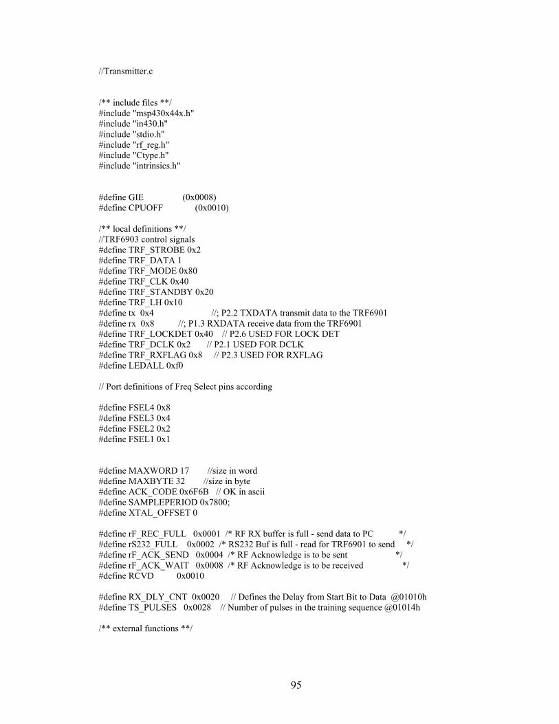
95
//Transmitter.c /** include files **/ #include "msp430x44x.h" #include "in430.h" #include "stdio.h" #include "rf_reg.h" #include "Ctype.h" #include "intrinsics.h" #define GIE (0x0008) #define CPUOFF (0x0010) /** local definitions **/ //TRF6903 control signals #define TRF_STROBE 0x2 #define TRF_DATA 1 #define TRF_MODE 0x80 #define TRF_CLK 0x40 #define TRF_STANDBY 0x20 #define TRF_LH 0x10 #define tx 0x4 //; P2.2 TXDATA transmit data to the TRF6901 #define rx 0x8 //; P1.3 RXDATA receive data from the TRF6901 #define TRF_LOCKDET 0x40 // P2.6 USED FOR LOCK DET #define TRF_DCLK 0x2 // P2.1 USED FOR DCLK #define TRF_RXFLAG 0x8 // P2.3 USED FOR RXFLAG #define LEDALL 0xf0 // Port definitions of Freq Select pins according #define FSEL4 0x8 #define FSEL3 0x4 #define FSEL2 0x2 #define FSEL1 0x1 #define MAXWORD 17 //size in word #define MAXBYTE 32 //size in byte #define ACK_CODE 0x6F6B // OK in ascii #define SAMPLEPERIOD 0x7800; #define XTAL_OFFSET 0 #define rF_REC_FULL 0x0001 /* RF RX buffer is full - send data to PC */ #define rS232_FULL 0x0002 /* RS232 Buf is full - read for TRF6901 to send */ #define rF_ACK_SEND 0x0004 /* RF Acknowledge is to be sent */ #define rF_ACK_WAIT 0x0008 /* RF Acknowledge is to be received */ #define RCVD 0x0010 #define RX_DLY_CNT 0x0020 // Defines the Delay from Start Bit to Data @01010h #define TS_PULSES 0x0028 // Number of pulses in the training sequence @01014h /** external functions **/
96
extern void Set_Clk(void); extern void Set_DCO(int); extern void program_TRF69(unsigned int, unsigned int); //trf6903.s43 extern void receive_RF(unsigned char, unsigned int *); extern void send_RF(unsigned int,unsigned int*); extern void rs232_link_send(unsigned int,unsigned int*); extern void finish(void); extern void configure_trf6903(void); extern void InitTRF6903(void); extern void wait_lockdet(void); /** external data **/ extern struct TRF_REG trf6903; extern int PreAmbleSize; /** internal functions **/ /** public data **/ int f_sel; int opstate; unsigned int DR_DLY_CNT = 0x003F; unsigned int DR_DLY_CNT2; unsigned int DR_DLY_CNT3; unsigned int PULSE_WIDTH_TOL; unsigned int START_WIDTH_TOL; /* k1, m1 and j1 are global variables used in UART RX ISR*/ int k1=1; int m1=0; unsigned int j1=MAXBYTE; /** private data **/ /** public functions **/ void InitIo(void); int GetFsel(void); void program_TRF6903_word(unsigned long ); void ChecksumGenTX(unsigned char num); void TBIntEnable(int); void rs232_report(void); /** private functions **/ struct RF_XMIT_PACKET int packetsize; unsigned int xmit[MAXWORD]; unsigned int rcv[MAXWORD]; unsigned int rs232buf[MAXWORD]; unsigned int chk[1]; // stores checksum generated at the receiver for the received data buf; unsigned int Btime; unsigned int Btime1_5; void main(void)
97
DR_DLY_CNT2 = DR_DLY_CNT -12 ; DR_DLY_CNT3 = DR_DLY_CNT2 * 3 ; PULSE_WIDTH_TOL = 0x18; START_WIDTH_TOL = PULSE_WIDTH_TOL * 3; WDTCTL = WDTPW+WDTHOLD;// Stop watchdog timer InitIo(); InitTRF6903(); Btime=64; Btime1_5=60; f_sel = GetFsel(); configure_trf6903(); buf.packetsize = 34; P6OUT &=~16; P4OUT &=~4; while(1) receive_RF(buf.packetsize,buf.rcv); TBIntEnable(0x0C00); // delay finish(); // end of while (1) // end of main void InitIo(void) int i; opstate|=0x00; // initilalize opstate P3OUT|=TRF_MODE; // MODE is set to output Direction P3OUT|=TRF_LH; // LEARN/HOLD is set to output Direction P1DIR|= LEDALL; P1OUT&= ~LEDALL; P1IES |= 0xf; // all int on high to low trans P2DIR|= tx; // TXDATA is set to output Direction P2SEL=0x33; //select UART functions for P2.4 and P2.5, select TimerA,TimerB capture for RXDATA and DCLK P3DIR|= TRF_CLK + TRF_STANDBY + TRF_MODE + TRF_LH; //P3 OUTPUT * Rest of the ports in Port 3 are Input direction (Fsel1 to Fsel4)* P3SEL|= 0x0; // P3 Input Output Mode P4DIR|= TRF_STROBE + TRF_DATA; //P4.0, P4.1 are output P4SEL|= 0x0; // P4 Input Output Mode P5DIR|= 0x0; // Port 5 is not used P5OUT|= 0x0; P5SEL|= 0x0;
98
P6OUT|=0xf; //All RSSI led off P6DIR|=0x1f; //RSSI LED driver configured as ouput P6SEL|=0x80; //RSSI is AD function TBCCR0|=DR_DLY_CNT; //load TBCCR0 for tx and rx data pulse width Set_DCO(30000); //set dco for 32Khz external watch * 75 = 2.4576 MHz=DCO Freq // After a PUC both SMCLK and MCLK are sourced by DCO freq at 2.4576 MHz //initialize UART port. Default Baud =38.4K UTCTL0=0x20; // Select SMCLk as the source for UART clock URCTL0=0x8; UBR00=0; // Baud Rate = 9600bps UBR10=0x01; UMCTL0=0x0; // No modulation . Since fractional divider is not used UMCTL0=0; UCTL0=0x11; // USART - UART Mode UCTL0&=0xfe; // Disable the UART initially ME1|=URXE0+UTXE0; //enable Transmitter + receiver IE1|=URXIE0; // Enable USART0 Receive Interrupt //blink All RSSI LED and Button LED to indicate power up condition for(i=0;i<30000;i++) P1OUT|=LEDALL; P6OUT&=0xf0; P1OUT&=~(LEDALL); for(i=0;i<30000;i++); //arbitrary wait P6OUT|=0xf; // RSSI LED Off int GetFsel(void) int in0, in1; in0 = P3IN&FSEL1; in0<<=3; in1 = P3IN & FSEL2; // Get remaining select in0|=(in1<<1); // align FSEL3 and FSEL2 in1 = P3IN & FSEL3; // align FSEL1 in0 |= in1>>1; in1=P3IN &FSEL4; in0|=in1>>3; in0=~in0; //reverse polarity in0=in0 & 0xf; return in0;
99
/* Used For RS232 Reception - USART 0 */ #pragma vector=USART0RX_VECTOR __interrupt void Usart0RxInt(void) int cnt2; TACTL&=0x22; // Stop Timer A and Disable Interrupt CCTL2&=CCIE; // Disable Timer_A CCR2 interrupt cnt2 = U0RXBUF; P5DIR = 0; P4DIR &=~4; P4OUT &=~4; if ((opstate&rS232_FULL) == 0) k1 = 0; for(m1 = 1; m1 < MAXWORD; m1++) for(j1 = 0; j1 < 100; j1++); cnt2 = P5IN; buf.xmit[m1] = cnt2; if(k1 ==1) k1 = 0; else k1 = 1; P6OUT = 16*k1; for(j1 = 0; j1 < 100; j1++); cnt2 = P5IN; buf.xmit[m1] |= (cnt2 << 8); if(k1 ==1) k1 = 0; else k1 = 1; P6OUT = 16*k1; for(j1 = 0; j1< 100; j1++); P6OUT|=0xf; // RSSI LED Off //Implement Redundancy for(j1 = 5; j1<MAXWORD; j1++) buf.xmit[j1] = buf.xmit[1]; asm(" BIC #00010h,2(SP)"); // wake up from sleep mode asm ("BIS #00008h,2(SP)"); // restore GIE
100
j1=32; // Initialize Receieve Counter k1=1; m1=0; opstate|=0x00; opstate|=rS232_FULL; asm("MOV #receive_RF,12(SP)"); // return in receive_RF routine asm("BIC #00018h,0(SP)"); // Wake from sleep mode ChecksumGenTX(16); send_RF(buf.packetsize,buf.xmit); rs232_report(); // end of Interrupt Service Routine /******************************************************************************* TimerB clock = 2.4576Mhz ******************************************************************************/ void TBIntEnable( int time) if((TBCTL&0x30)==0) //if the counter is halted TBCTL=0x204; //stop counter- timer running at SMCLK/1 = 2.4576 MHz TBR=0; //clear counter TBCTL=0x220; //continuous up //ms100_cnt=10; TBCCR1=(TBR + time) & 0xffff; //turn on the interrupt - Compare Mode TBCCTL1 =0x0010; //turn on the interrupt return; // Timer B Interrupt Service Routine. // The ISR does nothing. It just returns control to the TBIntEnable function // after the specified time interval is completed #pragma vector=TIMERB1_VECTOR __interrupt void Timer_B(void) if (TBIV == 2) TBCCTL1&=0xffed; /*********************Checksum_gen********************************************** ;for sending data through RF channel only
101
;The calling function must load counter with the data packet size in bytes ;******************************************************************************/ void ChecksumGenTX(unsigned char num) unsigned int sum,k; sum=0; for (k=1;k<=num;k++) sum+=buf.xmit[k]; buf.xmit[0]=sum; return; //Fills the RS232BUF with the Values to Display //RS232 rate is 9600bps void rs232_report(void) int sum; int u; int next; int first_digit; int second_digit; IFG1 = 0; // Comments will Indicate what is being printed buf.rs232buf[0] = 36; //'$' next = 70; //'F' buf.rs232buf[0] |= (next << 8); buf.rs232buf[1] = 77; //'M' next = 66; //'B' buf.rs232buf[1] |= (next << 8); //Display the Board Number, as an example we display 23 buf.rs232buf[2] = 50; //'2' next = 51; //'3' buf.rs232buf[2] |= (next << 8); buf.rs232buf[3] = 44; //',' next = 0; // NULL buf.rs232buf[3] |= (next << 8); // Display length, for now just use sensor number as length since // we do not have calibration data. buf.rs232buf[4] = (buf.xmit[1] / 1000)+ 48; // The thousands digit of the length next = ((buf.xmit[1] - (1000*(buf.xmit[1] / 1000))) / 100)+ 48; // Hundreds digit of the length buf.rs232buf[4] |= (next << 8);
buf.rs232buf[5] = ((buf.xmit[1] -(1000*(buf.xmit[1] / 1000))-(100*(buf.xmit[1] / 100))) / 10)+48; // Tens digit of Length
102
next = ((buf.xmit[1] -(1000*(buf.xmit[1] / 1000)))-(100*(buf.xmit[1] / 100)) - (10*(buf.xmit[1] / 10)))+ 48;
// Ones digit of Length buf.rs232buf[5] |= (next << 8); buf.rs232buf[6] = 44; //',' next = 0; // NULL buf.rs232buf[6] |= (next << 8); //Display Units either inches or mm if(buf.xmit[3] == 1) // mm case buf.rs232buf[7] = 109; //'m' next = 109; //'m' buf.rs232buf[7] |= (next << 8); if(buf.xmit[3] == 2) // inches case buf.rs232buf[7] = 73; //'I' next = 78; //'N' buf.rs232buf[7] |= (next << 8); buf.rs232buf[8] = 44; next = 0; buf.rs232buf[8] |= (next << 8); // Display Supply Voltage buf.rs232buf[9] = (buf.xmit[4] / 100)+ 48; //First Digit Display first_digit = (buf.xmit[4] / 100); next = 46; //'.' buf.rs232buf[9] |= (next << 8); buf.rs232buf[10] = ((buf.xmit[4] - (100*(buf.xmit[4] / 100))) / 10)+ 48; // Second Digit Display second_digit = ((buf.xmit[4] - (100*(buf.xmit[4] / 100))) / 10); next = (buf.xmit[4] - first_digit*100 - second_digit*10) +48; //Third Digit Display buf.rs232buf[10] |= (next << 8); buf.rs232buf[11] = 86; //'V' next = 44;//',' buf.rs232buf[11] |= (next << 8); //Netwok Status Determined by Checksum sum = 0; for(u = 1; u < MAXWORD; u++) sum+=buf.xmit[u]; if(sum == buf.xmit[0]) buf.rs232buf[12] = 49; next = 44;
103
buf.rs232buf[12] |= (next << 8); else buf.rs232buf[12] = 48; next = 44; buf.rs232buf[12] |= (next << 8); // Print the Status of the Sensors //Sensors are 'Good' if(buf.xmit[2] == 1) buf.rs232buf[13] = 71; next = 111; buf.rs232buf[13] |= (next << 8); buf.rs232buf[14] = 111; next = 100; buf.rs232buf[14] |= (next << 8); //Sensors are 'Fair' if(buf.xmit[2] == 2) buf.rs232buf[13] = 70; next = 97; buf.rs232buf[13] |= (next << 8); buf.rs232buf[14] = 105; next = 114; buf.rs232buf[14] |= (next << 8); //Sensors are 'Fail' if(buf.xmit[2] == 3) buf.rs232buf[13] = 70; next = 97; buf.rs232buf[13] |= (next << 8); buf.rs232buf[14] = 105; next = 108; buf.rs232buf[14] |= (next << 8); buf.rs232buf[15] = 13; // Carriage Return next = 10; // Line Feed buf.rs232buf[15] |= (next << 8); for(u = 16; u<MAXWORD; u++) buf.rs232buf[u] = 0; opstate|=rF_REC_FULL; rs232_link_send(32, buf.rs232buf);

104
opstate&=~rF_REC_FULL;
105
// Program_REG.c /************************************************************************************** RF_reg.c AUTHOR: Harsha Rao ***************************************************************************************/ /**************************** Programming the TRF6903 ************************************************** TX = Mode_0: A Word is programmed for FSK transmission (Mode bit =1) RX = Mode_1: B Word is programmed for FSK receive (Mode bit =0) ;*******************************************************************************************************/ #include "rf_reg.h" #include "msp430x44x.h" #include "in430.h" #include "stdio.h" #include "f_6903.h" #define ENABLE_DCLK 1 extern int f_sel,fsel_update; extern unsigned int DR_DLY_CNT; struct TRF_REG trf6903; extern void program_TRF69(unsigned int, unsigned int); //trf6903.s43 void program_TRF6903_word(unsigned long ); void configure_trf6903(void); void InitTRF6903(void); int PreAmbleSize; void InitTRF6903(void) trf6903.a.bit.BND = 2; //select 900Mhz trf6903.a.bit.CP_Acc=0; trf6903.a.bit.PI = 0; trf6903.a.bit.TX_RX0 = 1; //low on mode means transmit trf6903.a.bit.PA0=0; trf6903.a.bit.B_DIV_M0 = 68; //set to 902 trf6903.a.bit.A_DIV_M0 = 27 ; trf6903.a.bit.ADDR =0; //0x2854A2 trf6903.b.bit.DET_EN = 1; //start off disabled trf6903.b.bit.DET_THRESH = 0; //2.2V trf6903.b.bit.PARXED = 1; trf6903.b.bit.FSK_OOK=1; trf6903.b.bit.TX_RX1=0; //receive when mode input =high trf6903.b.bit.PA1=0; trf6903.b.bit.B_DIV_M1 = 68; trf6903.b.bit.A_DIV_M1 = 1;

106
trf6903.b.bit.ADDR=1; //0x685599 trf6903.c.bit.reserved = 0; //start off disabled trf6903.c.bit.REF_DIV_COEF = 48; trf6903.c.bit.ADDR = 2; trf6903.d.bit.reserved1 = 0; //start off disabled trf6903.d.bit.OOKXS = 0; //2.2V trf6903.d.bit.DEM_TUNE = 7; //6 trf6903.d.bit.PFD_reset=1; trf6903.d.bit.XTAL_Tune=6; //receive when mode input =high trf6903.d.bit.RXS=1; trf6903.d.bit.reserved2 = 0; trf6903.d.bit.ADDR = 3; //0XC0E000 trf6903.e.bit.reserved1 = 1; // trf6903.e.bit.PAI = 2; //Nominal trf6903.e.bit.TCOUNT = 5; //Minimum training = 4 times the value //trf6903.e.bit.TCOUNT =30 ; //Minimum training = 4 times the value trf6903.e.bit.TWO=0; //receive when mode input =high //#ifdef ENABLE_DCLK trf6903.e.bit.TXM = 1; //use DCLK to send data //#else // trf6903.e.bit.TXM = 0; //use RAW //#endif trf6903.e.bit.RXM = 3; if (DR_DLY_CNT == 0x007F) trf6903.e.bit.D3 = 0 ; trf6903.e.bit.D2 = 3 ; // 19.2 k trf6903.e.bit.D1 = 3 ; if (DR_DLY_CNT == 0x003F) trf6903.e.bit.D3 = 0 ; trf6903.e.bit.D2 = 2 ; // 38.4 k trf6903.e.bit.D1 = 3 ; if (DR_DLY_CNT == 0x002F) trf6903.e.bit.D3 = 0 ; trf6903.e.bit.D2 = 2 ; // 51.2 k trf6903.e.bit.D1 = 2 ; trf6903.e.bit.ADDR = 2; PreAmbleSize = trf6903.e.bit.TCOUNT; PreAmbleSize =(PreAmbleSize*4) + 100; void configure_trf6903(void) int pointer; P4OUT&=0xfe; //start with 0 on data
107
pointer=(int)f_sel; trf6903.a.bit.B_DIV_M0=MAIN_B_T[pointer]; trf6903.a.bit.A_DIV_M0=MAIN_A_T[pointer]; program_TRF6903_word(trf6903.a.all); trf6903.b.bit.B_DIV_M1=MAIN_B_R[pointer]; trf6903.b.bit.A_DIV_M1=MAIN_A_R[pointer]; program_TRF6903_word(trf6903.b.all); program_TRF6903_word(trf6903.c.all); trf6903.d.bit.XTAL_Tune = XTAL_OFFSET; program_TRF6903_word(trf6903.d.all); program_TRF6903_word(trf6903.e.all); void program_TRF6903_word(unsigned long control) unsigned int high,low; high = (unsigned int)(control>>16); low =(unsigned int)control; program_TRF69(high,low);
108
; set_dco.s43 ;This module sets the clock. ;================================================================================ #include "msp430x44x.h" #define Count1 R8 #define Count2 R9 MODULE Set_DCO PUBLIC Set_DCO RSEG CODE ;Adjust DCO Routine Set_DCO MOV.B #(75-1),&SCFQCTL_ MOV.B #FN_3,&SCFI0_ ;MOV.B #030h,&FLL_CTL0_ ;10pf load MOV.B #010h,&FLL_CTL0_ ;6pf load Set_DCO1 BIC.B #OFIFG,&IFG1_ NOT_COOKED MOV R12,Count1 ;20 is the wait time WAIT? DEC Count1 JNZ WAIT? BIT.B #OFIFG, &IFG1_ ;test oscillator fault flag JNZ Set_DCO ; Repeat until test flag remains reset MOV #WDTPW+WDTHOLD,&WDTCTL ; if start detected, WDT set to timeout every 52uS RET ENDMOD MODULE ReStart PUBLIC ReStart RSEG CODE ReStart MOV #0fffeh,R5 BR @R5 RET ENDMOD ; END // The Set_Clk routine is never called since XT2 OSC is not used on the demo board MODULE Set_Clk PUBLIC Set_Clk RSEG CODE

109
Set_Clk BIC.B #XT2OFF, &FLL_CTL1_ ; Turn on the High XT2 Xtal TST_OF BIC.B #OFIFG,&IFG1_ MOV #20,Count1 ;20 is the wait time LOOP DEC Count1 JNZ LOOP BIT.B #OFIFG, &IFG1_ ;test oscillator fault flag JNZ TST_OF ; Repeat until test flag remains reset MOV.B #SELM_XT2+SELS,&FLL_CTL1_ ; select the proper clock RET ENDMOD END
110
;trf6903_Registers.s43 /**************************** program_TRF69 ********************************************************** ; purpose: ; programs a word to A, B, C or D word register of the TRF6901 ; gets the settings from the calling routine in R6 and R7 ; ;*******************************************************************************************************/ #include "msp430x44x.h" #include "std_f43x.asm" #define Count1 R8 #define Count2 R9 #define counter R10 ; universal counter NAME TRF6901 RSEG CODE(1) PUBLIC program_TRF69 EXTERN ?CL430_1_23_L08 RSEG CODE program_TRF69 init_high_byte DINT PUSH R10 PUSH R9 PUSH R8 PUSH R7 PUSH R6 PUSH R5 PUSH R4 MOV R12,word_h ;mov data to appropriate register MOV R14,word_l BIC.B #strobe,&P4OUT ; reset Strobe port BIS.B #strobe,&P4DIR ; switch Strobe to output direction MOV #02h,counter ; initialize the counter for high and low byte MOV #08h,bits_r ; initialize bitcounter ; MOV word_h,word_trf MOV R6,R4 SWPB word_trf ; push the low byte to the high byte, only the ; data in the low byte is relevant JMP program_word

111
init_low_byte MOV #010h,bits_r ; initialize bitcounter ; MOV word_l,word_trf ; push the low byte to the programming buffer MOV R7,R4 program_word RLC word_trf ; push the msb of the programming buffer to carry JNC program_low program_high BIS.B #data,&P4OUT ; set data(P1.7) program_clock BIS.B #clk,&P3OUT ; generate a pulse on the clock line BIC.B #clk,&P3OUT program_next_bit DEC bits_r ; decrement bit counter JNZ program_word ; have already all bits been sent? DEC counter ; decrement counter for low byte recognition JNZ init_low_byte ; low byte is to be programmed generate_strobe BIC.B #data,&P4OUT ; reset data BIS.B #strobe,&P4OUT ; set strobe(P1.5) BIC.B #strobe,&P4OUT ; clear strobe(P1.5) BIC.B #strobe,&P4DIR ; set strobe(P1.5) to input direction POP R4 POP R5 POP R6 POP R7 POP R8 POP R9 POP R10 EINT RET ; back to calling routine program_low BIC.B #data,&P4OUT ; clear data(P1.7) JMP program_clock

112
end_program_TRF69 END
113
;WirelessUART_RF.s43 ;/**************************************************************** ; Author - Harsha Rao ;Interrupt subroutines and send and receive RF drivers ;****************************************************************/ #include "msp430x44x.h" #include "std_f43x.asm" #define rF_REC_FULL 0x0001 /* RF RX buffer is full - send data to PC */ #define rS232_FULL 0x0002 /* RS232 Buf is full - read for TRF6901 to send */ #define rF_ACK_SEND 0x0004 /* RF Acknowledge is to be sent */ #define rF_ACK_WAIT 0x0008 /* RF Acknowledge is to be received */ #define RCVD 0x0010 #define RSTAT R8 ; status of the reception #define wait_r R9 ; counter register for all waiting loops ***** #define counter R10 ; universal counter #define RX_DLY_CNT 0x0028 // Not Used in the Firmware #define TS_PULSES 0x0080 // Number of pulses in the training sequence @01014h*/ NAME radio(16) RSEG CODE(1) COMMON INTVEC(1) EXTERN time_out_count EXTERN opstate EXTERN DR_DLY_CNT EXTERN DR_DLY_CNT2 EXTERN DR_DLY_CNT3 EXTERN PULSE_WIDTH_TOL EXTERN START_WIDTH_TOL EXTERN k1 EXTERN m1 EXTERN j1 EXTERN Set_DCO EXTERN Btime EXTERN Btime1_5 PUBLIC Timer_A1 PUBLIC receive_RF PUBLIC send_RF PUBLIC rs232_link_send PUBLIC wait_lockdet PUBLIC finish EXTERN ?CL430_1_23_L08 RSEG CODE MOV #09F0h,SP
114
Timer_A1: ADD &TAIV,PC RETI RETI JMP CC2_INT ; RF reception -> every edge of ; the rx-signal RETI RETI ?back RETI ;************************************* Timer_B Interrupt routine *********** ; purpose: handle the Timer_B interrupts, and decide which dedicated routine ; should be addressed. (TB_CCR0 / RF reception and transmission) ;**************************************************************************** TimerB0 BIC #CPUOFF,0(SP) ; reactivate CPU end_TB_CCR0 RETI ;****************************** Capture Compare 2 Register ********************************************* ; used for RF-Reception ;******************************************************************************************************* CC2_INT ; used by biph_rx MOV RRFTAB(R8),PC ; conditional jump depends on RSTAT ; RSTAT = 0, detecting the Trianingsequence ; RSTAT = 1, Trainingsquence detected, waiting ; for the Start Bit ; RSTAT = 2, Start Bit detected, Data Reception RRFTAB DW RSTAT00 DW RSTAT01 DW RSTAT10 DW RSTAT11 RSTAT00 MOV &CCR2,R14 ; save Reference Capture value MOV R14,R15 ; copy Timer_A value SUB R13,R15 ; subtract the current Timer_A value from the ; old one -> Bitwidth in cycles in res_r MOV R14,R13 ; current value now -> old value later

115
test_res_r00 SUB DR_DLY_CNT2,R15 CMP PULSE_WIDTH_TOL,R15 ;4/18 is the detected signal 20-34uS long? JHS no_valid_pulse INCD R8 ; first valid pulse detected INC wake_up_counter ; count this valid pulse BIS #CCIE,&CCTL2 ; re-enable CCR2 interrupt JMP go_back no_valid_pulse CLR R8 ; no the signal doesn't fit the wakeup sequence CLR wake_up_counter ; reset the wake_up_counter, received an ; invalid pulse JMP go_back /******************************************************************************************************************************************/ RSTAT01 MOV &CCR2,R14 ; save Reference Capture value MOV R14,R15 ; copy Timer_A value SUB R13,R15 ; subtract the current Timer_A value from the ; old one -> Bitwidth in cycles in res_r MOV R14,R13 ; current value now -> old value later test_res_r01 SUB DR_DLY_CNT2,R15 CMP PULSE_WIDTH_TOL,R15 ;4/18 is the detected signal 20-34uS long? JHS no_valid_pulse INC wake_up_counter ; next valid pulse JMP go_back /*******************************************************************************************************************************************/ RSTAT10 MOV &CCR2,R14 ; save Reference Capture value MOV R14,R15 ; copy Timer_A value SUB R13,R15 ; subtract the current Timer_A value from ; the old one -> Bitwidth in cycles in res_r MOV R14,R13 ; current value now -> old value later

116
test_res_r10 SUB DR_DLY_CNT3,R15 ;CMP #038,R15 ; is the detected signal x cycles long? This is for asymmetric stuff CMP START_WIDTH_TOL,R15 JGE invalid_bit ; restart detection, this is not a valid sequence JHS no_start_int_enable INCD R8 ; go to RSTATE 2, Data Reception, Start Bit ; detected BIC #CCIE,&CCTL2 ; disable CCR2 interrupt BIC #022h,&TACTL ; stop Timer_A and disable interrupt no_start_bit INC wake_up_counter ; count the pulses of the trainings sequence, CMP #TS_PULSES,wake_up_counter ; compare the value of the counter with the JGE invalid_bit ; JMP go_back ;get ready for data collection no_start_int_enable JMP no_start_bit invalid_bit CLR R8 ; restart the detection, this is not a valid CLR wake_up_counter ; initialize the wake_up_counter go_back BIC #CPUOFF,0(SP) ; wake up! RETI /******************************************************************************************************************************************/ /* Not Used in this version of Firmware*/ /*****************************************************************************************************************************************/ RSTAT11 BIT #CAP,&CCTL2 ; if in capture mode, just found start bit JNZ R_start_edge_detected ; due to negative edge BIC.B #rx,&P2SEL ;make it into GPIO BIT.B #rx,&P2IN ;read IObit RLC data_r ; push carry into the data register BIS.B #rx,&P2SEL ;go back to module ADD &Btime,&CCR2 INC bits_r
117
CMP #010h,bits_r ; receive 16 bits in row JNE end_RSTAT11_INT ;get all bits BIC #CCIE,&CCTL2 ;no more int JMP end_RSTAT11_INT R_start_edge_detected BIC #CAP,&CCTL2 ;go to compare mode ADD &Btime1_5,&CCR2 ;get ready to receive data CLR bits_r end_RSTAT11_INT ; before the interrupt request, but start BIC #CPUOFF,0(SP) ; wake up! ; subroutine RETI kill_receive BIC #CCIE,&CCTL2 ; disable CCR2 interrupt BIC #022h,&TACTL ; stop Timer_A and disable interrupt BIC #CPUOFF,0(SP) ; wake up! RETI ;*********************************** send_RF *********************************************************** ; purpose: sends data through RF channel ;******************************************************************************************************* send_RF BIC.B #URXIFG0,&IFG1 ; Clear Receive Interrupt Flag BIC.B #URXIE0,&IE1 ; Disable USART1 Receive Interrupt send_RF_acknowledge? BIT #rF_ACK_SEND,&opstate ; has an acknowledge to be send? JNZ send_RF_init data_to_transmit? BIT #rS232_FULL,&opstate ; Is there any data to send via TRF6901? JZ end_send_RF ; No, nothing to send send_RF_init DINT MOV R12,R10 MOV R12,R6 ADD R14,R10 BIC.B #mode,&P3OUT ; Mode=0 -> Send mode BIC.B #tx,&P2OUT ; TXDATA(P2.2) is reset BIS.B #stdb_trf6901,&P3OUT ; TRF6900 active, STANDBY(P3.5) is high DECD R10 MOV 0(R10),data_r ; first word to the send register
118
;This is where clock recovery happens--DCLK has to be connected to the P2.1/TB0 pin MOV #0x4910,&TBCCTL0 ; enable TBCCR0 Interrupt, Capture on Positive Edge of DCLK ; MOV #0x8910,&TBCCTL0 ;capture on negative edge MOV #0x0224,&TBCTL ; enable TIMERB and start in Continous mode EINT send_RF_training_sequence ; the entire length ca. 4ms, 154 pulses MOV #TS_PULSES, tr_counter ; initialize the training sequence counter send1_RF_toggle BIS #CPUOFF+GIE,SR ; CPU off ;------------------ Start of the trainings sequence ---------------------------------------------------- XOR.B #tx,&P2OUT ; toggle TXDATA(P2.2) DEC tr_counter ; decrement counter for the training sequence JNZ send1_RF_toggle ; JMP send1_RF_toggle ; ADD TRIGGER HERE BIC.B #l_h,&P3OUT ; END TRIGGER send_RF_long_bit BIS #CPUOFF+GIE,SR ; CPU off ;------------------ Start of the start bit ------------------------------------------------------------- BIS.B #tx,&P2OUT ; start of the long start-bit 78,12ec BIS #CPUOFF+GIE,SR ; CPU off BIC #rS232_FULL,&opstate ; the RS232 buffer is ready for reception BIS #CPUOFF+GIE,SR ; CPU off BIS #CPUOFF+GIE,SR ; CPU off ;----------------- End of the start bit ---------------------------------------------------------------- start_bit_low BIC.B #tx,&P2OUT ; reset TXDATA(P2.2) MOV DR_DLY_CNT,wait_r INC wait_r RRA wait_r ; used for DIV by 2 send_pause_dly DEC wait_r JNZ send_pause_dly send_RF_data MOV #010h,bits_r ; init bitcounter, transmit first 16 bits send_RF_bit_test RLC data_r ; push the next data bit to carry
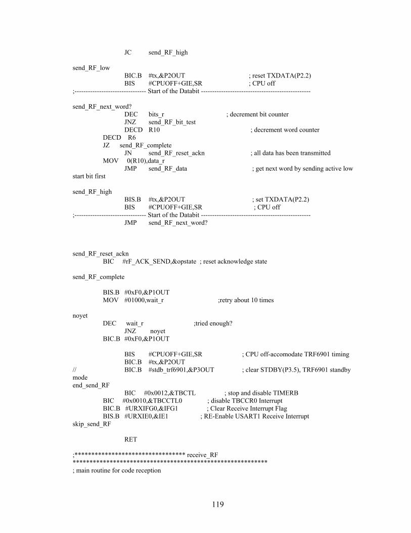
119
JC send_RF_high send_RF_low BIC.B #tx,&P2OUT ; reset TXDATA(P2.2) BIS #CPUOFF+GIE,SR ; CPU off ;-------------------------------- Start of the Databit ------------------------------------------------- send_RF_next_word? DEC bits_r ; decrement bit counter JNZ send_RF_bit_test DECD R10 ; decrement word counter DECD R6 JZ send_RF_complete JN send_RF_reset_ackn ; all data has been transmitted MOV 0(R10),data_r JMP send_RF_data ; get next word by sending active low start bit first send_RF_high BIS.B #tx,&P2OUT ; set TXDATA(P2.2) BIS #CPUOFF+GIE,SR ; CPU off ;-------------------------------- Start of the Databit ------------------------------------------------- JMP send_RF_next_word? send_RF_reset_ackn BIC #rF_ACK_SEND,&opstate ; reset acknowledge state send_RF_complete BIS.B #0xF0,&P1OUT MOV #01000,wait_r ;retry about 10 times noyet DEC wait_r ;tried enough? JNZ noyet BIC.B #0xF0,&P1OUT BIS #CPUOFF+GIE,SR ; CPU off-accomodate TRF6901 timing BIC.B #tx,&P2OUT // BIC.B #stdb_trf6901,&P3OUT ; clear STDBY(P3.5), TRF6901 standby mode end_send_RF BIC #0x0012,&TBCTL ; stop and disable TIMERB BIC #0x0010,&TBCCTL0 ; disable TBCCR0 Interrupt BIC.B #URXIFG0,&IFG1 ; Clear Receive Interrupt Flag BIS.B #URXIE0,&IE1 ; RE-Enable USART1 Receive Interrupt skip_send_RF RET ;********************************* receive_RF ********************************************************** ; main routine for code reception
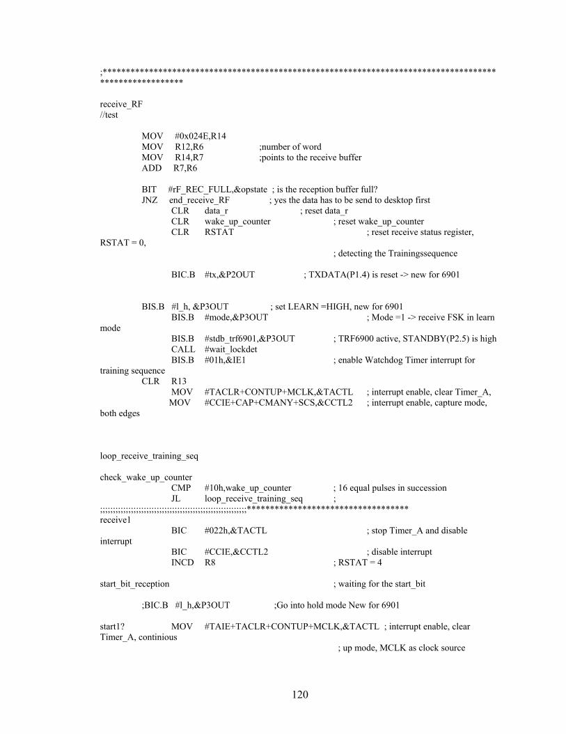
120
;******************************************************************************************************* receive_RF //test MOV #0x024E,R14 MOV R12,R6 ;number of word MOV R14,R7 ;points to the receive buffer ADD R7,R6 BIT #rF_REC_FULL,&opstate ; is the reception buffer full? JNZ end_receive_RF ; yes the data has to be send to desktop first CLR data_r ; reset data_r CLR wake_up_counter ; reset wake_up_counter CLR RSTAT ; reset receive status register, RSTAT = 0, ; detecting the Trainingssequence BIC.B #tx,&P2OUT ; TXDATA(P1.4) is reset -> new for 6901 BIS.B #l_h, &P3OUT ; set LEARN =HIGH, new for 6901 BIS.B #mode,&P3OUT ; Mode =1 -> receive FSK in learn mode BIS.B #stdb_trf6901,&P3OUT ; TRF6900 active, STANDBY(P2.5) is high CALL #wait_lockdet BIS.B #01h,&IE1 ; enable Watchdog Timer interrupt for training sequence CLR R13 MOV #TACLR+CONTUP+MCLK,&TACTL ; interrupt enable, clear Timer_A, MOV #CCIE+CAP+CMANY+SCS,&CCTL2 ; interrupt enable, capture mode, both edges loop_receive_training_seq check_wake_up_counter CMP #10h,wake_up_counter ; 16 equal pulses in succession JL loop_receive_training_seq ; ;;;;;;;;;;;;;;;;;;;;;;;;;;;;;;;;;;;;;;;;;;;;;;;;;;;;;;;;;*********************************** receive1 BIC #022h,&TACTL ; stop Timer_A and disable interrupt BIC #CCIE,&CCTL2 ; disable interrupt INCD R8 ; RSTAT = 4 start_bit_reception ; waiting for the start_bit ;BIC.B #l_h,&P3OUT ;Go into hold mode New for 6901 start1? MOV #TAIE+TACLR+CONTUP+MCLK,&TACTL ; interrupt enable, clear Timer_A, continious ; up mode, MCLK as clock source
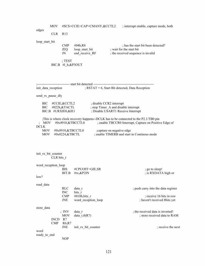
121
MOV #SCS+CCIE+CAP+CMANY,&CCTL2 ; interrupt enable, capture mode, both edges CLR R13 loop_start_bit CMP #04h,R8 ; has the start bit been detected? JEQ loop_start_bit ; wait for the start bit JN end_receive_RF ; the received sequence is invalid ; TEST BIC.B #l_h,&P3OUT ;----------------------------- start bit detected ------------------------------------------------------ init_data_reception ; RSTAT = 6, Start Bit detected, Data Reception send_rx_pause_dly BIC #CCIE,&CCTL2 ; disable CCR2 interrupt BIC #022h,&TACTL ; stop Timer_A and disable interrupt BIC.B #URXIE0,&IE1 ; Disable USART1 Receive Interrupt ;This is where clock recovery happens--DCLK has to be connected to the P2.1/TB0 pin ; MOV #0x4910,&TBCCTL0 ; enable TBCCR0 Interrupt, Capture on Positive Edge of DCLK MOV #0x8910,&TBCCTL0 ;capture on negative edge MOV #0x0224,&TBCTL ; enable TIMERB and start in Continous mode init_rx_bit_counter CLR bits_r word_reception_loop BIS #CPUOFF+GIE,SR ; go to sleep! BIT.B #rx,&P2IN ; is RXDATA high or low? read_data RLC data_r ; push carry into the data register INC bits_r CMP #010h,bits_r ; receive 16 bits in row JNE word_reception_loop ; haven't received 8bits yet store_data ; INV data_r ; the received data is inverted! MOV data_r,0(R7) ; store received data to RAM INCD R7 CMP R6,R7 JNE init_rx_bit_counter ; receive the next word ready_to_end NOP
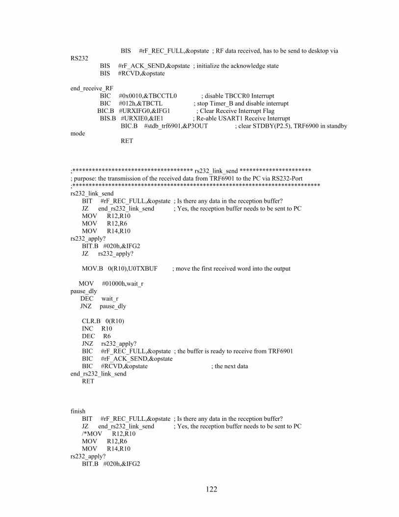
122
BIS #rF_REC_FULL,&opstate ; RF data received, has to be send to desktop via RS232 BIS #rF_ACK_SEND,&opstate ; initialize the acknowledge state BIS #RCVD,&opstate end_receive_RF BIC #0x0010,&TBCCTL0 ; disable TBCCR0 Interrupt BIC #012h,&TBCTL ; stop Timer_B and disable interrupt BIC.B #URXIFG0,&IFG1 ; Clear Receive Interrupt Flag BIS.B #URXIE0,&IE1 ; Re-able USART1 Receive Interrupt BIC.B #stdb_trf6901,&P3OUT ; clear STDBY(P2.5), TRF6900 in standby mode RET ;************************************* rs232_link_send ********************** ; purpose: the transmission of the received data from TRF6901 to the PC via RS232-Port ;**************************************************************************** rs232_link_send BIT #rF_REC_FULL,&opstate ; Is there any data in the reception buffer? JZ end_rs232_link_send ; Yes, the reception buffer needs to be sent to PC MOV R12,R10 MOV R12,R6 MOV R14,R10 rs232_apply? BIT.B #020h,&IFG2 JZ rs232_apply? MOV.B 0(R10),U0TXBUF ; move the first received word into the output MOV #01000h,wait_r pause_dly DEC wait_r JNZ pause_dly CLR.B 0(R10) INC R10 DEC R6 JNZ rs232_apply? BIC #rF_REC_FULL,&opstate ; the buffer is ready to receive from TRF6901 BIC #rF_ACK_SEND,&opstate BIC #RCVD,&opstate ; the next data end_rs232_link_send RET finish BIT #rF_REC_FULL,&opstate ; Is there any data in the reception buffer? JZ end_rs232_link_send ; Yes, the reception buffer needs to be sent to PC /*MOV R12,R10 MOV R12,R6 MOV R14,R10 rs232_apply? BIT.B #020h,&IFG2
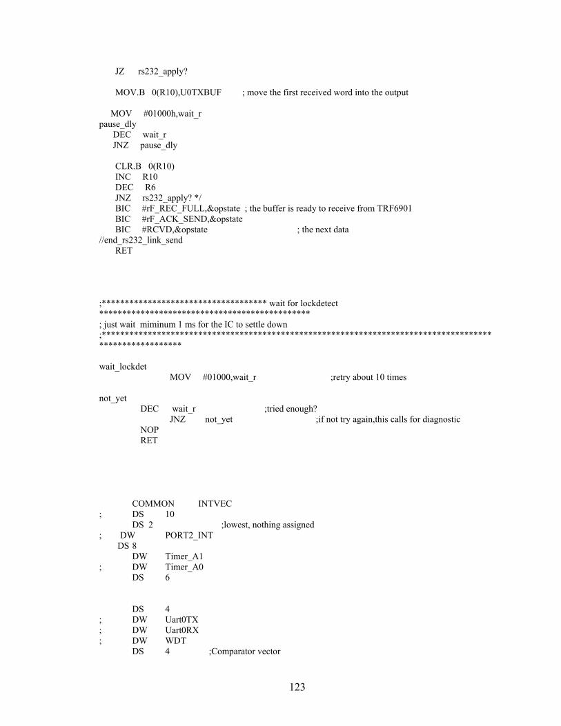
123
JZ rs232_apply? MOV.B 0(R10),U0TXBUF ; move the first received word into the output MOV #01000h,wait_r pause_dly DEC wait_r JNZ pause_dly CLR.B 0(R10) INC R10 DEC R6 JNZ rs232_apply? */ BIC #rF_REC_FULL,&opstate ; the buffer is ready to receive from TRF6901 BIC #rF_ACK_SEND,&opstate BIC #RCVD,&opstate ; the next data //end_rs232_link_send RET ;************************************ wait for lockdetect ********************************************** ; just wait miminum 1 ms for the IC to settle down ;******************************************************************************************************* wait_lockdet MOV #01000,wait_r ;retry about 10 times not_yet DEC wait_r ;tried enough? JNZ not_yet ;if not try again,this calls for diagnostic NOP RET COMMON INTVEC ; DS 10 DS 2 ;lowest, nothing assigned ; DW PORT2_INT DS 8 DW Timer_A1 ; DW Timer_A0 DS 6 DS 4 ; DW Uart0TX ; DW Uart0RX ; DW WDT DS 4 ;Comparator vector

124
; DW TImerB1 ;timer B1 handled DW TimerB0 ; DS NMI_VECTOR ; DS RESET_VECTOR END

125
APPENDIX C: RECEPTION
What follows is the code necessary for the receiving microcontroller, the files included are:
11. Receiver.c 12. Program_Reg.c 13. SetDCO.s43 14. trf6903_Registers.s43 15. WirelessUART_RF.s43
Of these programs, we edited trf6903_WirelessUART.c written by Harsha Rao of TI and made it Transmitter.c, the other files are completely written by Harsha Rao as a part of the “Single-Channel Firmware” which can be found at [33]. Slight edits are made to WirelessUART_RF.s43.

126
// receiver.c /** include files **/ #include "msp430x44x.h" #include "in430.h" #include "stdio.h" #include "rf_reg.h" #include "Ctype.h" #include "intrinsics.h" #define GIE (0x0008) #define CPUOFF (0x0010) /** local definitions **/ //TRF6903 control signals #define TRF_STROBE 0x2 #define TRF_DATA 1 #define TRF_MODE 0x80 #define TRF_CLK 0x40 #define TRF_STANDBY 0x20 #define TRF_LH 0x10 #define tx 0x4 //; P2.2 TXDATA transmit data to the TRF6901 #define rx 0x8 //; P1.3 RXDATA receive data from the TRF6901 #define TRF_LOCKDET 0x40 // P2.6 USED FOR LOCK DET #define TRF_DCLK 0x2 // P2.1 USED FOR DCLK #define TRF_RXFLAG 0x8 // P2.3 USED FOR RXFLAG #define LEDALL 0xf0 // Port definitions of Freq Select pins according #define FSEL4 0x8 #define FSEL3 0x4 #define FSEL2 0x2 #define FSEL1 0x1 #define MAXWORD 17 //size in word #define MAXBYTE 32 //size in byte #define ACK_CODE 0x6F6B // OK in ascii #define SAMPLEPERIOD 0x7800; #define XTAL_OFFSET 0 #define rF_REC_FULL 0x0001 /* RF RX buffer is full - send data to PC */ #define rS232_FULL 0x0002 /* RS232 Buf is full - read for TRF6901 to send */ #define rF_ACK_SEND 0x0004 /* RF Acknowledge is to be sent */ #define rF_ACK_WAIT 0x0008 /* RF Acknowledge is to be received */ #define RCVD 0x0010 #define RX_DLY_CNT 0x0020 // Defines the Delay from Start Bit to Data @01010h #define TS_PULSES 0x0028 // Number of pulses in the training sequence @01014h /** external functions **/ extern void Set_Clk(void);
127
extern void Set_DCO(int); extern void program_TRF69(unsigned int, unsigned int); //trf6903.s43 extern void receive_RF(unsigned char, unsigned int *); extern void send_RF(unsigned int,unsigned int*); extern void rs232_link_send(unsigned int,unsigned int*); extern void configure_trf6903(void); extern void InitTRF6903(void); /** external data **/ extern struct TRF_REG trf6903; extern int PreAmbleSize; /** internal functions **/ /** public data **/ int f_sel; int opstate; unsigned int DR_DLY_CNT = 0x003F; unsigned int DR_DLY_CNT2; unsigned int DR_DLY_CNT3; unsigned int PULSE_WIDTH_TOL; unsigned int START_WIDTH_TOL; /* k1, m1 and j1 are global variables used in UART RX ISR*/ int k1=1; int m1=0; int j1=MAXBYTE; struct majority int length; int num_of_votes; decision; unsigned int received[MAXWORD]; /** private data **/ /** public functions **/ void InitIo(void); int GetFsel(void); void program_TRF6903_word(unsigned long ); void checksum_r(void); void ChecksumGenRX(unsigned char num); void TBIntEnable(int); void majority_vote(); void rs232_report(void); /** private functions **/ struct RF_XMIT_PACKET int packetsize; unsigned int xmit[MAXWORD]; unsigned int rcv[MAXWORD]; unsigned int rs232buf[MAXWORD];
128
unsigned int chk[1]; // stores checksum generated at the receiver for the received data buf; unsigned int Btime; unsigned int Btime1_5; void main(void) DR_DLY_CNT2 = DR_DLY_CNT -12 ; DR_DLY_CNT3 = DR_DLY_CNT2 * 3 ; PULSE_WIDTH_TOL = 0x18; START_WIDTH_TOL = PULSE_WIDTH_TOL * 3; WDTCTL = WDTPW+WDTHOLD;// Stop watchdog timer InitIo(); InitTRF6903(); Btime=64; Btime1_5=60; f_sel = GetFsel(); configure_trf6903(); buf.packetsize = 34; decision.num_of_votes = 0; decision.length = 0; while(1) receive_RF(buf.packetsize,buf.rcv); checksum_r(); rs232_report(); TBIntEnable(0x0C00); // delay opstate = 0; // end of while (1) // end of main /************************************* checksum_r **************************** ; purpose: the checksum of the received data package from RF, ; for reliable data transmission ;****************************************************************************/ void checksum_r(void) if((opstate&rF_ACK_WAIT)==0) // IF RX routine not expecting ack //Generate checksum at the receiver - store the result( 1 byte in an array buf.chk[0]) ChecksumGenRX(16); // Generate chksum of the received data and store it in buf.chk return; else return; // Initializes all I/O Ports void InitIo(void)
129
int i; opstate|=0x00; // initilalize opstate P3OUT|=TRF_MODE; // MODE is set to output Direction P3OUT|=TRF_LH; // LEARN/HOLD is set to output Direction P1DIR|= LEDALL; P1OUT&= ~LEDALL; P1IES |= 0xf; // all int on high to low trans P2DIR|= tx; // TXDATA is set to output Direction P2SEL=0x33; //select UART functions for P2.4 and P2.5, select TimerA,TimerB capture for RXDATA and DCLK P3DIR|= TRF_CLK + TRF_STANDBY + TRF_MODE + TRF_LH; //P3 OUTPUT * Rest of the ports in Port 3 are Input direction (Fsel1 to Fsel4)* P3SEL|= 0x0; // P3 Input Output Mode P4DIR|= TRF_STROBE + TRF_DATA; //P4.0, P4.1 are output P4SEL|= 0x0; // P4 Input Output Mode P5DIR|= 0x0; // Port 5 is not used P5OUT|= 0x0; P5SEL|= 0x0; P6OUT|=0xf; //All RSSI led off P6DIR|=0xf; //RSSI LED driver configured as ouput P6SEL|=0x80; //RSSI is AD function TBCCR0|=DR_DLY_CNT; //load TBCCR0 for tx and rx data pulse width Set_DCO(30000); //set dco for 32Khz external watch * 75 = 2.4576 MHz=DCO Freq // After a PUC both SMCLK and MCLK are sourced by DCO freq at 2.4576 MHz //initialize UART port. Default Baud =38.4K UTCTL0=0x20; // Select SMCLk as the source for UART clock URCTL0=0x8; UBR00=0x40; // Baud rate = 2.4576 MHz/64 = 38.4kbps // UBR00=0x80; // Baud rate = 2.4576 MHz/128 = 19.2kbps UBR10=0; /*Use the definitions below for different serial port rates. The GUI can be used to transfer data at the speified rate UBR00=0x80; // Baud rate = 2.4576 MHz/64 = 19.2kbps UBR00=0x10; // Baud rate = 2.4576 MHz/21 = 115.2kbps UBR00=0x80; // Baud rate = 2.4576 MHz/256 = 9.6kbps UBR10=0x80; // NOTE THAT BOTH UBR0 and UBR1 are used */ UMCTL0=0x0; // No modulation . Since fractional divider is not used UMCTL0=0;
130
UCTL0=0x11; // USART - UART Mode UCTL0&=0xfe; // Disable the UART initially ME1|=URXE0+UTXE0; //enable Transmitter + receiver IE1|=URXIE0; // Enable USART0 Receive Interrupt //blink All RSSI LED and Button LED to indicate power up condition for(i=0;i<30000;i++) P1OUT|=LEDALL; P6OUT&=0xf0; P1OUT&=~(LEDALL); for(i=0;i<30000;i++); //arbitrary wait P6OUT|=0xf; // RSSI LED Off int GetFsel(void) int in0, in1; in0 = P3IN&FSEL1; in0<<=3; in1 = P3IN & FSEL2; // Get remaining select in0|=(in1<<1); // align FSEL3 and FSEL2 in1 = P3IN & FSEL3; // align FSEL1 in0 |= in1>>1; in1=P3IN &FSEL4; in0|=in1>>3; in0=~in0; //reverse polarity in0=in0 & 0xf; return in0; /******************************************************************************* TimerB clock = 2.4576Mhz ******************************************************************************/ void TBIntEnable( int time) if((TBCTL&0x30)==0) //if the counter is halted TBCTL=0x204; //stop counter- timer running at SMCLK/1 = 2.4576 MHz TBR=0; //clear counter TBCTL=0x220; //continuous up //ms100_cnt=10; TBCCR1=(TBR + time) & 0xffff; //turn on the interrupt - Compare Mode TBCCTL1 =0x0010; //turn on the interrupt return;

131
// Timer B Interrupt Service Routine. // The ISR does nothing. It just returns control to the TBIntEnable function // after the specified time interval is completed #pragma vector=TIMERB1_VECTOR __interrupt void Timer_B(void) if (TBIV == 2) TBCCTL1&=0xffed; /*********************Checksum_gen********************************************** ;for sending data through RF channel only ;The calling function must load counter with the data packet size in bytes ;******************************************************************************/ void ChecksumGenRX(unsigned char num) unsigned int sum,k; sum=0; for (k=0;k<num;k++) sum+=buf.rcv[k]; buf.chk[0]=sum; return; void majority_vote(void) int n; int i; int next = 1; int length_value[13] = 0; int votes[13] = 0; int voted = 0; int max = 0; length_value[0] = buf.rcv[15]; votes[0]++; for(n = 0; n<MAXWORD-5; n++) for(i = 0; i<next;i++) if(buf.rcv[n] == length_value[i]) votes[i]++; voted = 1;
132
break; if(voted == 0) length_value[next] = buf.rcv[n]; votes[next]++; next++; voted = 0; //Determine which entry has the highest Vote for(n = 0; n<MAXWORD - 5; n++) if(max<votes[n]) decision.length = length_value[n]; decision.num_of_votes = votes[n]; max = votes[n]; //Fills the RS232BUF with the Values to Display //RS232 rate is 9600bps void rs232_report(void) int u; int next; int first_digit; int second_digit; IFG1 = 0; majority_vote(); // Comments will Indicate what is being printed buf.rs232buf[0] = 36; //'$' next = 70; //'F' buf.rs232buf[0] |= (next << 8); buf.rs232buf[1] = 77; //'M' next = 66; //'B' buf.rs232buf[1] |= (next << 8); //Display the Board Number, as an example we display 23 buf.rs232buf[2] = 50; //'2' next = 51; //'3' buf.rs232buf[2] |= (next << 8); buf.rs232buf[3] = 44; //',' next = 0; // NULL buf.rs232buf[3] |= (next << 8);
133
// Display length, for now just use sensor number as length since // we do not have calibration data. //In thesis explain the /1000 and *1000, b/c it does the truncation for you!!!!!!!!!!!!! buf.rs232buf[4] = (decision.length / 1000)+ 48; // The thousands digit of the length next = ((decision.length - (1000*(decision.length / 1000))) / 100)+ 48; // Hundreds digit of the length buf.rs232buf[4] |= (next << 8); buf.rs232buf[5] = ((decision.length -(1000*(decision.length / 1000))-(100*(decision.length / 100))) / 10)+48; // Tens digit of Length next = ((decision.length -(1000*(decision.length / 1000)))-(100*(decision.length / 100)) - (10*(decision.length / 10)))+ 48; // Ones digit of Length buf.rs232buf[5] |= (next << 8); buf.rs232buf[6] = 44; //',' next = 0; // NULL buf.rs232buf[6] |= (next << 8); //Display Units either inches or mm if(buf.rcv[13] == 1) // mm case buf.rs232buf[7] = 109; //'m' next = 109; //'m' buf.rs232buf[7] |= (next << 8); if(buf.rcv[13] == 2) // inches case buf.rs232buf[7] = 73; //'I' next = 78; //'N' buf.rs232buf[7] |= (next << 8); buf.rs232buf[8] = 44; next = 0; buf.rs232buf[8] |= (next << 8); // Display Supply Voltage buf.rs232buf[9] = (buf.rcv[12] / 100)+ 48; //First Digit Display first_digit = (buf.rcv[12] / 100); next = 46; //'.' buf.rs232buf[9] |= (next << 8); buf.rs232buf[10] = ((buf.rcv[12] - (100*(buf.rcv[12] / 100))) / 10)+ 48; // Second Digit Display second_digit = ((buf.rcv[12] - (100*(buf.rcv[12] / 100))) / 10); next = (buf.rcv[12] - first_digit*100 - second_digit*10) +48; //Third Digit Display buf.rs232buf[10] |= (next << 8); buf.rs232buf[11] = 86; //'V' next = 44;//',' buf.rs232buf[11] |= (next << 8); //Netwok Status Determined by Votes and Checksum
134
first_digit = decision.num_of_votes/10; buf.rs232buf[12] = 48+first_digit; next = 48+(decision.num_of_votes - first_digit*10); buf.rs232buf[12] |= (next << 8); buf.rs232buf[13] = 44; if ((buf.chk[0] == buf.rcv[16])) next = 49; // Display '1' if Checksum Correect else next = 48; // Display '0' if Checksum Incorrect buf.rs232buf[13] |= (next << 8); buf.rs232buf[14] = 44; for(u = 15; u<MAXWORD; u++) buf.rs232buf[u] = 0; opstate|=rF_REC_FULL; rs232_link_send(32, buf.rs232buf); opstate&=~rF_REC_FULL; // Print the Status of the Sensors in the next transmission //Sensors are 'Good' if(buf.rcv[14] == 1) buf.rs232buf[0] = 71; next = 111; buf.rs232buf[0] |= (next << 8); buf.rs232buf[1] = 111; next = 100; buf.rs232buf[1] |= (next << 8); //Sensors are 'Fair' if(buf.rcv[14] == 2) buf.rs232buf[0] = 70; next = 97; buf.rs232buf[0] |= (next << 8); buf.rs232buf[1] = 105; next = 114; buf.rs232buf[1] |= (next << 8); //Sensors are 'Fail' if(buf.rcv[14] == 3) buf.rs232buf[0] = 70; next = 97; buf.rs232buf[0] |= (next << 8); buf.rs232buf[1] = 105;
135
next = 108; buf.rs232buf[1] |= (next << 8); buf.rs232buf[2] = 13; // Carriage Return next = 10; // Line Feed buf.rs232buf[2] |= (next << 8); for(u = 3; u<MAXWORD; u++) buf.rs232buf[u] = 0; opstate|=rF_REC_FULL; rs232_link_send(32, buf.rs232buf); for(u = 0; u<MAXWORD;u++) buf.rs232buf[u] = 0; //opstate&=~rF_REC_FULL;

136
//Program_Reg.c /************************************************************************************** RF_reg.c AUTHOR: Harsha Rao ***************************************************************************************/ /**************************** Programming the TRF6903 ************************************************** TX = Mode_0: A Word is programmed for FSK transmission (Mode bit =1) RX = Mode_1: B Word is programmed for FSK receive (Mode bit =0) ;*******************************************************************************************************/ #include "rf_reg.h" #include "msp430x44x.h" #include "in430.h" #include "stdio.h" #include "f_6903.h" #define ENABLE_DCLK 1 extern int f_sel,fsel_update; extern unsigned int DR_DLY_CNT; struct TRF_REG trf6903; extern void program_TRF69(unsigned int, unsigned int); //trf6903.s43 void program_TRF6903_word(unsigned long ); void configure_trf6903(void); void InitTRF6903(void); int PreAmbleSize; void InitTRF6903(void) trf6903.a.bit.BND = 2; //select 900Mhz trf6903.a.bit.CP_Acc=0; trf6903.a.bit.PI = 0; trf6903.a.bit.TX_RX0 = 1; //low on mode means transmit trf6903.a.bit.PA0=0; trf6903.a.bit.B_DIV_M0 = 68; //set to 902 trf6903.a.bit.A_DIV_M0 = 27 ; trf6903.a.bit.ADDR =0; //0x2854A2 trf6903.b.bit.DET_EN = 1; //start off disabled trf6903.b.bit.DET_THRESH = 0; //2.2V trf6903.b.bit.PARXED = 1; trf6903.b.bit.FSK_OOK=1; trf6903.b.bit.TX_RX1=0; //receive when mode input =high trf6903.b.bit.PA1=0; trf6903.b.bit.B_DIV_M1 = 68; trf6903.b.bit.A_DIV_M1 = 1;
137
trf6903.b.bit.ADDR=1; //0x685599 trf6903.c.bit.reserved = 0; //start off disabled trf6903.c.bit.REF_DIV_COEF = 48; trf6903.c.bit.ADDR = 2; trf6903.d.bit.reserved1 = 0; //start off disabled trf6903.d.bit.OOKXS = 0; //2.2V trf6903.d.bit.DEM_TUNE = 7; //6 trf6903.d.bit.PFD_reset=1; trf6903.d.bit.XTAL_Tune=6; //receive when mode input =high trf6903.d.bit.RXS=1; trf6903.d.bit.reserved2 = 0; trf6903.d.bit.ADDR = 3; //0XC0E000 trf6903.e.bit.reserved1 = 1; // trf6903.e.bit.PAI = 2; //Nominal trf6903.e.bit.TCOUNT = 5; //Minimum training = 4 times the value //trf6903.e.bit.TCOUNT =30 ; //Minimum training = 4 times the value trf6903.e.bit.TWO=0; //receive when mode input =high //#ifdef ENABLE_DCLK trf6903.e.bit.TXM = 1; //use DCLK to send data //#else // trf6903.e.bit.TXM = 0; //use RAW //#endif trf6903.e.bit.RXM = 3; if (DR_DLY_CNT == 0x007F) trf6903.e.bit.D3 = 0 ; trf6903.e.bit.D2 = 3 ; // 19.2 k trf6903.e.bit.D1 = 3 ; if (DR_DLY_CNT == 0x003F) trf6903.e.bit.D3 = 0 ; trf6903.e.bit.D2 = 2 ; // 38.4 k trf6903.e.bit.D1 = 3 ; if (DR_DLY_CNT == 0x002F) trf6903.e.bit.D3 = 0 ; trf6903.e.bit.D2 = 2 ; // 51.2 k trf6903.e.bit.D1 = 2 ; trf6903.e.bit.ADDR = 2; PreAmbleSize = trf6903.e.bit.TCOUNT; PreAmbleSize =(PreAmbleSize*4) + 100; void configure_trf6903(void) int pointer; P4OUT&=0xfe; //start with 0 on data
138
pointer=(int)f_sel; trf6903.a.bit.B_DIV_M0=MAIN_B_T[pointer]; trf6903.a.bit.A_DIV_M0=MAIN_A_T[pointer]; program_TRF6903_word(trf6903.a.all); trf6903.b.bit.B_DIV_M1=MAIN_B_R[pointer]; trf6903.b.bit.A_DIV_M1=MAIN_A_R[pointer]; program_TRF6903_word(trf6903.b.all); program_TRF6903_word(trf6903.c.all); trf6903.d.bit.XTAL_Tune = XTAL_OFFSET; program_TRF6903_word(trf6903.d.all); program_TRF6903_word(trf6903.e.all); void program_TRF6903_word(unsigned long control) unsigned int high,low; high = (unsigned int)(control>>16); low =(unsigned int)control; program_TRF69(high,low);

139
; set_dco.s43 ;This module sets the clock. ;================================================================================ #include "msp430x44x.h" #define Count1 R8 #define Count2 R9 MODULE Set_DCO PUBLIC Set_DCO RSEG CODE ;Adjust DCO Routine Set_DCO MOV.B #(75-1),&SCFQCTL_ MOV.B #FN_3,&SCFI0_ ;MOV.B #030h,&FLL_CTL0_ ;10pf load MOV.B #010h,&FLL_CTL0_ ;6pf load Set_DCO1 BIC.B #OFIFG,&IFG1_ NOT_COOKED MOV R12,Count1 ;20 is the wait time WAIT? DEC Count1 JNZ WAIT? BIT.B #OFIFG, &IFG1_ ;test oscillator fault flag JNZ Set_DCO ; Repeat until test flag remains reset MOV #WDTPW+WDTHOLD,&WDTCTL ; if start detected, WDT set to timeout every 52uS RET ENDMOD MODULE ReStart PUBLIC ReStart RSEG CODE ReStart MOV #0fffeh,R5 BR @R5 RET ENDMOD ; END // The Set_Clk routine is never called since XT2 OSC is not used on the demo board MODULE Set_Clk PUBLIC Set_Clk RSEG CODE
140
Set_Clk BIC.B #XT2OFF, &FLL_CTL1_ ; Turn on the High XT2 Xtal TST_OF BIC.B #OFIFG,&IFG1_ MOV #20,Count1 ;20 is the wait time LOOP DEC Count1 JNZ LOOP BIT.B #OFIFG, &IFG1_ ;test oscillator fault flag JNZ TST_OF ; Repeat until test flag remains reset MOV.B #SELM_XT2+SELS,&FLL_CTL1_ ; select the proper clock RET ENDMOD END
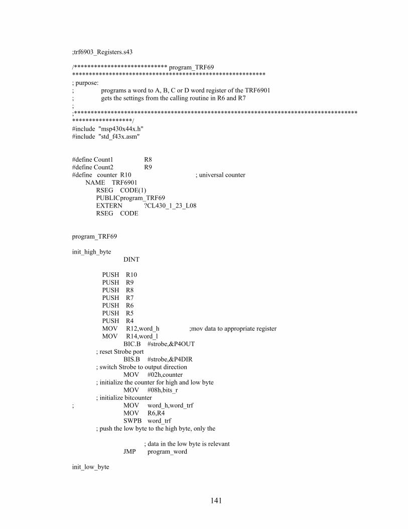
141
;trf6903_Registers.s43 /**************************** program_TRF69 ********************************************************** ; purpose: ; programs a word to A, B, C or D word register of the TRF6901 ; gets the settings from the calling routine in R6 and R7 ; ;*******************************************************************************************************/ #include "msp430x44x.h" #include "std_f43x.asm" #define Count1 R8 #define Count2 R9 #define counter R10 ; universal counter NAME TRF6901 RSEG CODE(1) PUBLIC program_TRF69 EXTERN ?CL430_1_23_L08 RSEG CODE program_TRF69 init_high_byte DINT PUSH R10 PUSH R9 PUSH R8 PUSH R7 PUSH R6 PUSH R5 PUSH R4 MOV R12,word_h ;mov data to appropriate register MOV R14,word_l BIC.B #strobe,&P4OUT ; reset Strobe port BIS.B #strobe,&P4DIR ; switch Strobe to output direction MOV #02h,counter ; initialize the counter for high and low byte MOV #08h,bits_r ; initialize bitcounter ; MOV word_h,word_trf MOV R6,R4 SWPB word_trf ; push the low byte to the high byte, only the ; data in the low byte is relevant JMP program_word init_low_byte

142
MOV #010h,bits_r ; initialize bitcounter ; MOV word_l,word_trf ; push the low byte to the programming buffer MOV R7,R4 program_word RLC word_trf ; push the msb of the programming buffer to carry JNC program_low program_high BIS.B #data,&P4OUT ; set data(P1.7) program_clock BIS.B #clk,&P3OUT ; generate a pulse on the clock line BIC.B #clk,&P3OUT program_next_bit DEC bits_r ; decrement bit counter JNZ program_word ; have already all bits been sent? DEC counter ; decrement counter for low byte recognition JNZ init_low_byte ; low byte is to be programmed generate_strobe BIC.B #data,&P4OUT ; reset data BIS.B #strobe,&P4OUT ; set strobe(P1.5) BIC.B #strobe,&P4OUT ; clear strobe(P1.5) BIC.B #strobe,&P4DIR ; set strobe(P1.5) to input direction POP R4 POP R5 POP R6 POP R7 POP R8 POP R9 POP R10 EINT RET ; back to calling routine program_low BIC.B #data,&P4OUT ; clear data(P1.7) JMP program_clock

143
end_program_TRF69 END
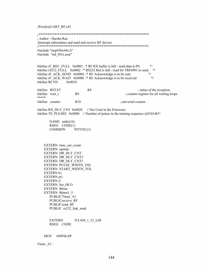
144
;WirelessUART_RF.s43 ;/**************************************************************** ; Author - Harsha Rao ;Interrupt subroutines and send and receive RF drivers ;****************************************************************/ #include "msp430x44x.h" #include "std_f43x.asm" #define rF_REC_FULL 0x0001 /* RF RX buffer is full - send data to PC */ #define rS232_FULL 0x0002 /* RS232 Buf is full - read for TRF6901 to send */ #define rF_ACK_SEND 0x0004 /* RF Acknowledge is to be sent */ #define rF_ACK_WAIT 0x0008 /* RF Acknowledge is to be received */ #define RCVD 0x0010 #define RSTAT R8 ; status of the reception #define wait_r R9 ; counter register for all waiting loops ***** #define counter R10 ; universal counter #define RX_DLY_CNT 0x0028 // Not Used in the Firmware #define TS_PULSES 0x0080 // Number of pulses in the training sequence @01014h*/ NAME radio(16) RSEG CODE(1) COMMON INTVEC(1) EXTERN time_out_count EXTERN opstate EXTERN DR_DLY_CNT EXTERN DR_DLY_CNT2 EXTERN DR_DLY_CNT3 EXTERN PULSE_WIDTH_TOL EXTERN START_WIDTH_TOL EXTERN k1 EXTERN m1 EXTERN j1 EXTERN Set_DCO EXTERN Btime EXTERN Btime1_5 PUBLIC Timer_A1 PUBLIC receive_RF PUBLIC send_RF PUBLIC rs232_link_send EXTERN ?CL430_1_23_L08 RSEG CODE MOV #09F0h,SP Timer_A1:

145
ADD &TAIV,PC RETI RETI JMP CC2_INT ; RF reception -> every edge of ; the rx-signal RETI RETI ?back RETI ;************************************* Timer_B Interrupt routine *********** ; purpose: handle the Timer_B interrupts, and decide which dedicated routine ; should be addressed. (TB_CCR0 / RF reception and transmission) ;**************************************************************************** TimerB0 BIC #CPUOFF,0(SP) ; reactivate CPU end_TB_CCR0 RETI ;****************************** Capture Compare 2 Register ********************************************* ; used for RF-Reception ;******************************************************************************************************* CC2_INT ; used by biph_rx MOV RRFTAB(R8),PC ; conditional jump depends on RSTAT ; RSTAT = 0, detecting the Trianingsequence ; RSTAT = 1, Trainingsquence detected, waiting ; for the Start Bit ; RSTAT = 2, Start Bit detected, Data Reception RRFTAB DW RSTAT00 DW RSTAT01 DW RSTAT10 DW RSTAT11 RSTAT00 MOV &CCR2,R14 ; save Reference Capture value MOV R14,R15 ; copy Timer_A value SUB R13,R15 ; subtract the current Timer_A value from the ; old one -> Bitwidth in cycles in res_r MOV R14,R13 ; current value now -> old value later
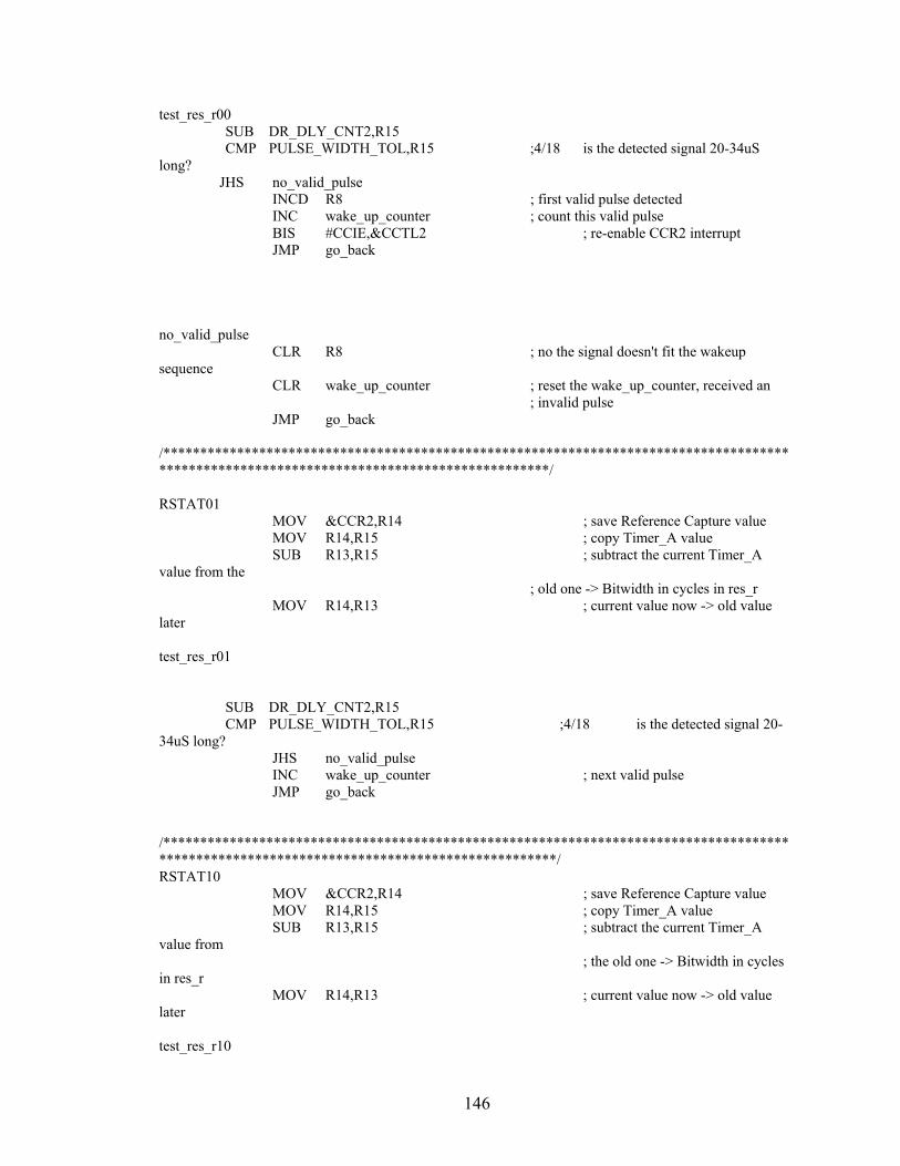
146
test_res_r00 SUB DR_DLY_CNT2,R15 CMP PULSE_WIDTH_TOL,R15 ;4/18 is the detected signal 20-34uS long? JHS no_valid_pulse INCD R8 ; first valid pulse detected INC wake_up_counter ; count this valid pulse BIS #CCIE,&CCTL2 ; re-enable CCR2 interrupt JMP go_back no_valid_pulse CLR R8 ; no the signal doesn't fit the wakeup sequence CLR wake_up_counter ; reset the wake_up_counter, received an ; invalid pulse JMP go_back /******************************************************************************************************************************************/ RSTAT01 MOV &CCR2,R14 ; save Reference Capture value MOV R14,R15 ; copy Timer_A value SUB R13,R15 ; subtract the current Timer_A value from the ; old one -> Bitwidth in cycles in res_r MOV R14,R13 ; current value now -> old value later test_res_r01 SUB DR_DLY_CNT2,R15 CMP PULSE_WIDTH_TOL,R15 ;4/18 is the detected signal 20-34uS long? JHS no_valid_pulse INC wake_up_counter ; next valid pulse JMP go_back /*******************************************************************************************************************************************/ RSTAT10 MOV &CCR2,R14 ; save Reference Capture value MOV R14,R15 ; copy Timer_A value SUB R13,R15 ; subtract the current Timer_A value from ; the old one -> Bitwidth in cycles in res_r MOV R14,R13 ; current value now -> old value later test_res_r10
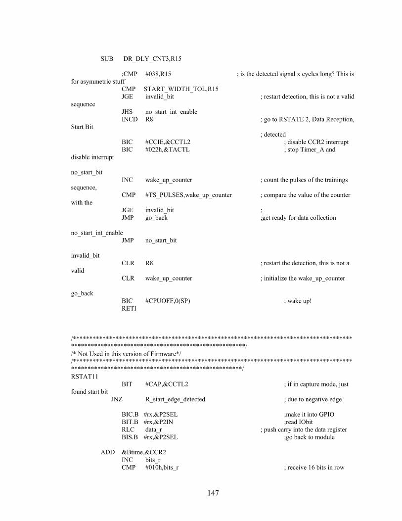
147
SUB DR_DLY_CNT3,R15 ;CMP #038,R15 ; is the detected signal x cycles long? This is for asymmetric stuff CMP START_WIDTH_TOL,R15 JGE invalid_bit ; restart detection, this is not a valid sequence JHS no_start_int_enable INCD R8 ; go to RSTATE 2, Data Reception, Start Bit ; detected BIC #CCIE,&CCTL2 ; disable CCR2 interrupt BIC #022h,&TACTL ; stop Timer_A and disable interrupt no_start_bit INC wake_up_counter ; count the pulses of the trainings sequence, CMP #TS_PULSES,wake_up_counter ; compare the value of the counter with the JGE invalid_bit ; JMP go_back ;get ready for data collection no_start_int_enable JMP no_start_bit invalid_bit CLR R8 ; restart the detection, this is not a valid CLR wake_up_counter ; initialize the wake_up_counter go_back BIC #CPUOFF,0(SP) ; wake up! RETI /******************************************************************************************************************************************/ /* Not Used in this version of Firmware*/ /*****************************************************************************************************************************************/ RSTAT11 BIT #CAP,&CCTL2 ; if in capture mode, just found start bit JNZ R_start_edge_detected ; due to negative edge BIC.B #rx,&P2SEL ;make it into GPIO BIT.B #rx,&P2IN ;read IObit RLC data_r ; push carry into the data register BIS.B #rx,&P2SEL ;go back to module ADD &Btime,&CCR2 INC bits_r CMP #010h,bits_r ; receive 16 bits in row

148
JNE end_RSTAT11_INT ;get all bits BIC #CCIE,&CCTL2 ;no more int JMP end_RSTAT11_INT R_start_edge_detected BIC #CAP,&CCTL2 ;go to compare mode ADD &Btime1_5,&CCR2 ;get ready to receive data CLR bits_r end_RSTAT11_INT ; before the interrupt request, but start BIC #CPUOFF,0(SP) ; wake up! ; subroutine RETI kill_receive BIC #CCIE,&CCTL2 ; disable CCR2 interrupt BIC #022h,&TACTL ; stop Timer_A and disable interrupt BIC #CPUOFF,0(SP) ; wake up! RETI ;*********************************** send_RF *********************************************************** ; purpose: sends data through RF channel ;******************************************************************************************************* send_RF BIC.B #URXIFG0,&IFG1 ; Clear Receive Interrupt Flag BIC.B #URXIE0,&IE1 ; Disable USART1 Receive Interrupt send_RF_acknowledge? BIT #rF_ACK_SEND,&opstate ; has an acknowledge to be send? JNZ send_RF_init data_to_transmit? BIT #rS232_FULL,&opstate ; Is there any data to send via TRF6901? JZ end_send_RF ; No, nothing to send send_RF_init DINT MOV R12,R10 MOV R12,R6 ADD R14,R10 BIC.B #mode,&P3OUT ; Mode=0 -> Send mode BIC.B #tx,&P2OUT ; TXDATA(P2.2) is reset BIS.B #stdb_trf6901,&P3OUT ; TRF6900 active, STANDBY(P3.5) is high DECD R10 MOV 0(R10),data_r ; first word to the send register
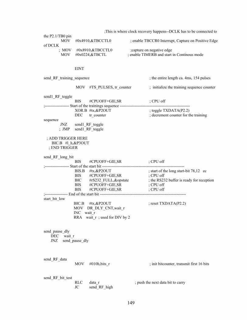
149
;This is where clock recovery happens--DCLK has to be connected to the P2.1/TB0 pin MOV #0x4910,&TBCCTL0 ; enable TBCCR0 Interrupt, Capture on Positive Edge of DCLK ; MOV #0x8910,&TBCCTL0 ;capture on negative edge MOV #0x0224,&TBCTL ; enable TIMERB and start in Continous mode EINT send_RF_training_sequence ; the entire length ca. 4ms, 154 pulses MOV #TS_PULSES, tr_counter ; initialize the training sequence counter send1_RF_toggle BIS #CPUOFF+GIE,SR ; CPU off ;------------------ Start of the trainings sequence ---------------------------------------------------- XOR.B #tx,&P2OUT ; toggle TXDATA(P2.2) DEC tr_counter ; decrement counter for the training sequence JNZ send1_RF_toggle ; JMP send1_RF_toggle ; ADD TRIGGER HERE BIC.B #l_h,&P3OUT ; END TRIGGER send_RF_long_bit BIS #CPUOFF+GIE,SR ; CPU off ;------------------ Start of the start bit ------------------------------------------------------------- BIS.B #tx,&P2OUT ; start of the long start-bit 78,12ec BIS #CPUOFF+GIE,SR ; CPU off BIC #rS232_FULL,&opstate ; the RS232 buffer is ready for reception BIS #CPUOFF+GIE,SR ; CPU off BIS #CPUOFF+GIE,SR ; CPU off ;----------------- End of the start bit ---------------------------------------------------------------- start_bit_low BIC.B #tx,&P2OUT ; reset TXDATA(P2.2) MOV DR_DLY_CNT,wait_r INC wait_r RRA wait_r ; used for DIV by 2 send_pause_dly DEC wait_r JNZ send_pause_dly send_RF_data MOV #010h,bits_r ; init bitcounter, transmit first 16 bits send_RF_bit_test RLC data_r ; push the next data bit to carry JC send_RF_high
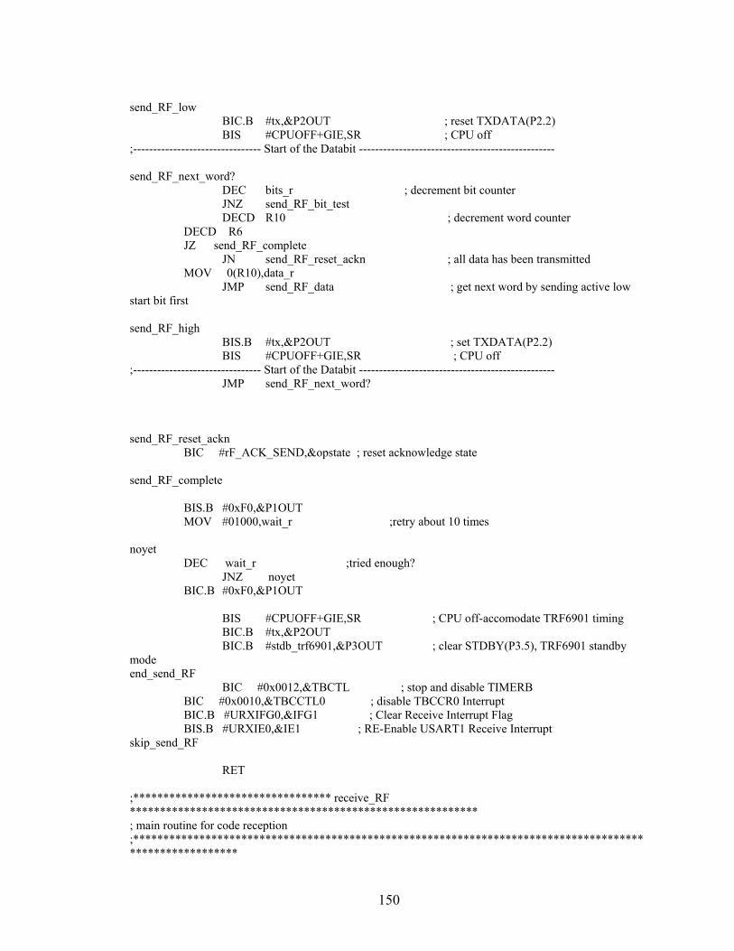
150
send_RF_low BIC.B #tx,&P2OUT ; reset TXDATA(P2.2) BIS #CPUOFF+GIE,SR ; CPU off ;-------------------------------- Start of the Databit ------------------------------------------------- send_RF_next_word? DEC bits_r ; decrement bit counter JNZ send_RF_bit_test DECD R10 ; decrement word counter DECD R6 JZ send_RF_complete JN send_RF_reset_ackn ; all data has been transmitted MOV 0(R10),data_r JMP send_RF_data ; get next word by sending active low start bit first send_RF_high BIS.B #tx,&P2OUT ; set TXDATA(P2.2) BIS #CPUOFF+GIE,SR ; CPU off ;-------------------------------- Start of the Databit ------------------------------------------------- JMP send_RF_next_word? send_RF_reset_ackn BIC #rF_ACK_SEND,&opstate ; reset acknowledge state send_RF_complete BIS.B #0xF0,&P1OUT MOV #01000,wait_r ;retry about 10 times noyet DEC wait_r ;tried enough? JNZ noyet BIC.B #0xF0,&P1OUT BIS #CPUOFF+GIE,SR ; CPU off-accomodate TRF6901 timing BIC.B #tx,&P2OUT BIC.B #stdb_trf6901,&P3OUT ; clear STDBY(P3.5), TRF6901 standby mode end_send_RF BIC #0x0012,&TBCTL ; stop and disable TIMERB BIC #0x0010,&TBCCTL0 ; disable TBCCR0 Interrupt BIC.B #URXIFG0,&IFG1 ; Clear Receive Interrupt Flag BIS.B #URXIE0,&IE1 ; RE-Enable USART1 Receive Interrupt skip_send_RF RET ;********************************* receive_RF ********************************************************** ; main routine for code reception ;*******************************************************************************************************
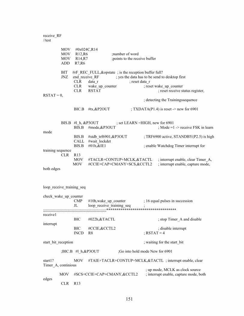
151
receive_RF //test MOV #0x024C,R14 MOV R12,R6 ;number of word MOV R14,R7 ;points to the receive buffer ADD R7,R6 BIT #rF_REC_FULL,&opstate ; is the reception buffer full? JNZ end_receive_RF ; yes the data has to be send to desktop first CLR data_r ; reset data_r CLR wake_up_counter ; reset wake_up_counter CLR RSTAT ; reset receive status register, RSTAT = 0, ; detecting the Trainingssequence BIC.B #tx,&P2OUT ; TXDATA(P1.4) is reset -> new for 6901 BIS.B #l_h, &P3OUT ; set LEARN =HIGH, new for 6901 BIS.B #mode,&P3OUT ; Mode =1 -> receive FSK in learn mode BIS.B #stdb_trf6901,&P3OUT ; TRF6900 active, STANDBY(P2.5) is high CALL #wait_lockdet BIS.B #01h,&IE1 ; enable Watchdog Timer interrupt for training sequence CLR R13 MOV #TACLR+CONTUP+MCLK,&TACTL ; interrupt enable, clear Timer_A, MOV #CCIE+CAP+CMANY+SCS,&CCTL2 ; interrupt enable, capture mode, both edges loop_receive_training_seq check_wake_up_counter CMP #10h,wake_up_counter ; 16 equal pulses in succession JL loop_receive_training_seq ; ;;;;;;;;;;;;;;;;;;;;;;;;;;;;;;;;;;;;;;;;;;;;;;;;;;;;;;;;;*********************************** receive1 BIC #022h,&TACTL ; stop Timer_A and disable interrupt BIC #CCIE,&CCTL2 ; disable interrupt INCD R8 ; RSTAT = 4 start_bit_reception ; waiting for the start_bit ;BIC.B #l_h,&P3OUT ;Go into hold mode New for 6901 start1? MOV #TAIE+TACLR+CONTUP+MCLK,&TACTL ; interrupt enable, clear Timer_A, continious ; up mode, MCLK as clock source MOV #SCS+CCIE+CAP+CMANY,&CCTL2 ; interrupt enable, capture mode, both edges CLR R13
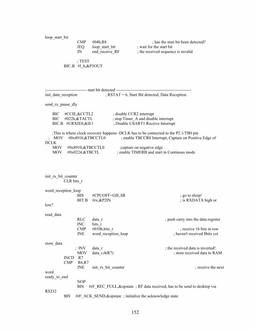
152
loop_start_bit CMP #04h,R8 ; has the start bit been detected? JEQ loop_start_bit ; wait for the start bit JN end_receive_RF ; the received sequence is invalid ; TEST BIC.B #l_h,&P3OUT ;----------------------------- start bit detected ------------------------------------------------------ init_data_reception ; RSTAT = 6, Start Bit detected, Data Reception send_rx_pause_dly BIC #CCIE,&CCTL2 ; disable CCR2 interrupt BIC #022h,&TACTL ; stop Timer_A and disable interrupt BIC.B #URXIE0,&IE1 ; Disable USART1 Receive Interrupt ;This is where clock recovery happens--DCLK has to be connected to the P2.1/TB0 pin ; MOV #0x4910,&TBCCTL0 ; enable TBCCR0 Interrupt, Capture on Positive Edge of DCLK MOV #0x8910,&TBCCTL0 ;capture on negative edge MOV #0x0224,&TBCTL ; enable TIMERB and start in Continous mode init_rx_bit_counter CLR bits_r word_reception_loop BIS #CPUOFF+GIE,SR ; go to sleep! BIT.B #rx,&P2IN ; is RXDATA high or low? read_data RLC data_r ; push carry into the data register INC bits_r CMP #010h,bits_r ; receive 16 bits in row JNE word_reception_loop ; haven't received 8bits yet store_data ; INV data_r ; the received data is inverted! MOV data_r,0(R7) ; store received data to RAM INCD R7 CMP R6,R7 JNE init_rx_bit_counter ; receive the next word ready_to_end NOP BIS #rF_REC_FULL,&opstate ; RF data received, has to be send to desktop via RS232 BIS #rF_ACK_SEND,&opstate ; initialize the acknowledge state
153
BIS #RCVD,&opstate end_receive_RF BIC #0x0010,&TBCCTL0 ; disable TBCCR0 Interrupt BIC #012h,&TBCTL ; stop Timer_B and disable interrupt BIC.B #URXIFG0,&IFG1 ; Clear Receive Interrupt Flag BIS.B #URXIE0,&IE1 ; Re-able USART1 Receive Interrupt BIC.B #stdb_trf6901,&P3OUT ; clear STDBY(P2.5), TRF6900 in standby mode RET ;************************************* rs232_link_send ********************** ; purpose: the transmission of the received data from TRF6901 to the PC via RS232-Port ;**************************************************************************** rs232_link_send BIT #rF_REC_FULL,&opstate ; Is there any data in the reception buffer? JZ end_rs232_link_send ; Yes, the reception buffer needs to be sent to PC MOV R12,R10 MOV R12,R6 MOV R14,R10 rs232_apply? BIT.B #020h,&IFG2 JZ rs232_apply? MOV.B 0(R10),U0TXBUF ; move the first received word into the output MOV #01000h,wait_r pause_dly DEC wait_r JNZ pause_dly CLR.B 0(R10) INC R10 DEC R6 JNZ rs232_apply? BIC #rF_REC_FULL,&opstate ; the buffer is ready to receive from TRF6901 BIC #rF_ACK_SEND,&opstate BIC #RCVD,&opstate ; the next data end_rs232_link_send RET ;************************************ wait for lockdetect ********************************************** ; just wait miminum 1 ms for the IC to settle down ;******************************************************************************************************* wait_lockdet MOV #01000,wait_r ;retry about 10 times
154
not_yet DEC wait_r ;tried enough? JNZ not_yet ;if not try again,this calls for diagnostic NOP RET COMMON INTVEC ; DS 10 DS 2 ;lowest, nothing assigned ; DW PORT2_INT DS 8 DW Timer_A1 ; DW Timer_A0 DS 6 DS 4 ; DW Uart0TX ; DW Uart0RX ; DW WDT DS 4 ;Comparator vector ; DW TImerB1 ;timer B1 handled DW TimerB0 ; DS NMI_VECTOR ; DS RESET_VECTOR END
155
REFERENCES
[1] WildCo, “Fish Measuring Board,” WildCo, [Online]. Available: http://www.wildco.com/vw_prdct_mdl.asp?prdct_mdl_cd=118. [Accessed: Mar. 21 2006]. [2] Limnoterra, “Electronic Fish Measuring Systems Design Specifications,” Limnoterra, [Online]. Available: http://www.limnoterragroup.com/fmb/design2.html. [Accessed: Mar. 21 2006]. [3] Scantrol, “Electronic Fish Sampling Board For Efficient Fish Sampling,” Scantrol, [Online]. Available: http://www.scantrol.net/FishMeter.htm. [Accessed: Mar. 21 2006]. [4] Juniper Systems, Inc., “Lat. 37 wFMB Wireless Fish Measuring Board,” Juniper Systems, Inc., [Online]. Avaliable: http://www.junipersys.com/files/wireless_fish_measuring_board.pdf [Accessed: Mar. 21 2006]. [5] SLAS344D MSP430x43x, MSP430x44x Datasheet Dallas, Tx: Texas Instruments, 2004. [6] DS39609B PIC18F6520/8520/6620/8620/6720/8720 Datasheet Chandler, Az: Microchip Technology Inc., 2004. [7] MC68HC16Y1TS/D Rev. 1 Technical Summary 16-Bit Modular Microcontroller MC68HC16Y1 Datasheet Phoenix, Az: Motorola Inc., 1996. [8] SLAU056D MSP430x4xx Family. User’s Guide Dallas, Tx: Texas Instruments, 2003. [9] M. Mano, Computer System Architecture, Englewood Cliffs: Prentice Hall, 1982. [10] D. S. Nyce, Linear Position Sensors: Theory and Applications, Hoboken, NJ: John Wiley and Sons, 2004. [11] Honeywell International Inc., “SS41,” January 2006, Available:http://catalog.sensing.honeywell.com/printfriendly.asp? FAM=solidstate&PN=SS41 [Accessed: Mar. 31 2006]. [12] Honeywell International Inc., “2SS52M,” January 2006, Available: http://catalog.sensing.honeywell.com/printfriendly.asp?FAM=solidstate& PN=2SS52M [Accessed: Mar. 31 2006].
156
[13] Catalog No. 480-1999-ND, Honeywell International Inc., Digi-Key Corporation, Thief River Falls, MN. [14] Catalog No. 480-1997-ND, Honeywell International Inc., Digi-Key Corporation, Thief River Falls, MN. [15] J.R. Carstens, Electrical Sensors and Transducers, Englewood Cliffs: Prentice Hall, 1993. [16] Honeywell, Hall-Effect Sensing and Application, Jan. 2004. [17] Allegro A1321 Data Sheet, Allegro Microsystems Inc., Dec. 2005. [18] Allegro Microsystems Inc., Appl. Note: 27701B, Sep. 1999. [19] Allegro Microsystems Inc., Appl. Note: 27702A*, April 1999. [20] D. Pozar, Microwave and RF Design of Wireless Systems, New York: John Wiley and Sons, 2001 [21] Smithson, G., "Introduction to digital modulation schemes," The Design of Digital Cellular Handsets (Ref. No. 1998/240), IEE Colloquium on , vol., no.pp.2/1-2/9, 4 Mar 1998. [22] H. Rao, “Implementing a Bidirectional Wireless UART Application With TRF6903 and MSP430,” Texas Instruments, 2004. [23] Mitra, A., "Bit error analysis of new generation wireless transceivers," Communication Systems, 2002. ICCS 2002. The 8th International Conference on, vol.2, no.pp. 636- 640 vol.2, 25-28 Nov. 2002. [24] TRF6903 Data sheet, Texas Instruments, Mar. 2005. [25] Chipcon CC1020 Data sheet, Chipcon Products from Texas Instruments, Feb. 2006. [26] ES Series RF Receiver Module Data Guide, Linx Technologies, Sept. 2005. [27] ES Series RF Transmitter Module Data Guide, Linx Technologies, Nov. 2005. [28] ADF7025 Data Sheet, Analog Devices Inc., Feb. 2006. [29] K. Chang, RF and Mircrowave Wireless Systems, New York: John Wiley and Sons, 2000. [30] M. Loy, “Understanding and Enhancing Sensitivity in Receivers for Wireless
157
Applications, Texas Instruments Application Note, SWRA030”, TX, US, 1999. [31] R. E. Collin, Antennas and Radiowave Propagation, New York, NY: McGraw- Hill Book Company, 1985. [32] Mobile Mark, “PSTN-900,” Mobile Mark, Nov. 2004. [33] Texas Instruments, “ISM Band Application Notes Abstract from Texas Instruments,” Texas Instruments [Online]. Available: http://focus.ti.com/analog/ docs/techdocsabstract.tsp?familyId=368&abstractName=swra039. [Accessed: April 13, 2006].