Embed Size (px)
Citation preview

1
Leuven Nano-Conference – LNC'07
Leuven, College De Valk
June 5-6, 2007
Jointly organized by
the Institute for Nanoscale Physics and Chemistry (INPAC)
the K.U.Leuven Materials Research Centre
(Leuven-MRC)
and
IMEC – Leuven
ABSTRACT BOOK

2
Index
Scope of the conference 3
Organization 3
Venue-Location 4
Programme Matrix 5
Programme
Oral presentations (June 5) 6
Oral presentations (June 6) 7
Posters 25
List of Participants 27

3
Scope of the conference:
The scope of the LNC'07 conference is focused on the effects of nanostructuring on materials'
properties resulting in development of new materials, products and devices that demonstrate new
functionalities. The topics covered also include fundamental relation between nanoscale
confinement of charge, spin and photon and the electrical, magnetic optical and chemical
properties of nanostructured inorganic, organic and bio-materials; the processing and properties
of materials for nano-electronics and nanoporeous materials. Nano-technology based applications
will be discussed, among others molecular healthcare, energy production and storage, catalysis
and ICT.
This conference is organized jointly by the Institute for Nanoscale Physics and Chemistry (INPAC-
K.U.Leuven), the Leuven Materials Research Center (Leuven-MRC - K.U.Leuven) and the
Interuniversity Microelectronics Center (IMEC). These research centers have a strong common
interest in nanoscience and nanotechnology, and therefore co-organize this event.
Conference Chairmen:
V.V. Moshchalkov (INPAC), R. Mertens (IMEC), I. Verpoest (Leuven-MRC)
Advisory and Programme committee:
G. Borghs (IMEC)
B. Goderis (Leuven-MRC)
P. Lievens (INPAC / LeuvenMRC)
J. Martens (Leuven-MRC
A. Vantomme (INPAC / Leuven-MRC)
M. Van der Auweraer (INPAC)
M. Van Rossum (IMEC
Conference Secretaries:
J. Vanacken, K. Van Acker
Local organizing committee:
M. Van Meerbeek, J. Herczeg
4
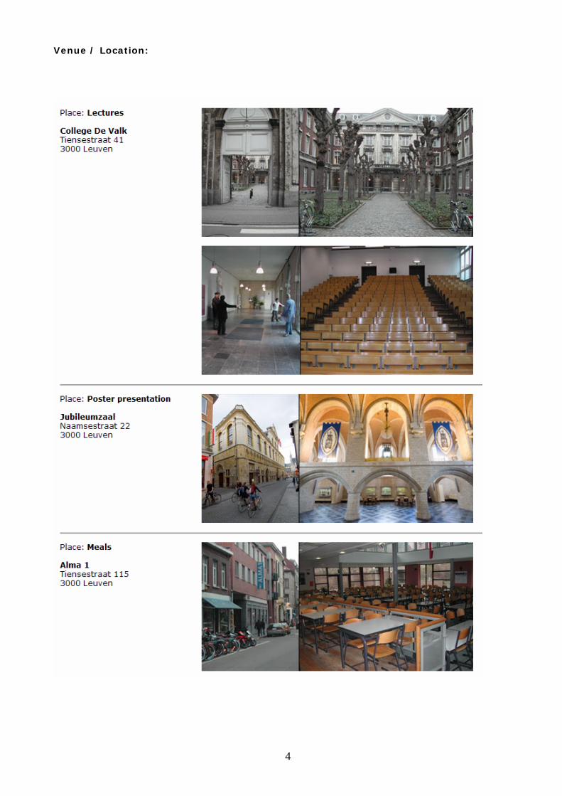
Venue / Location:
5
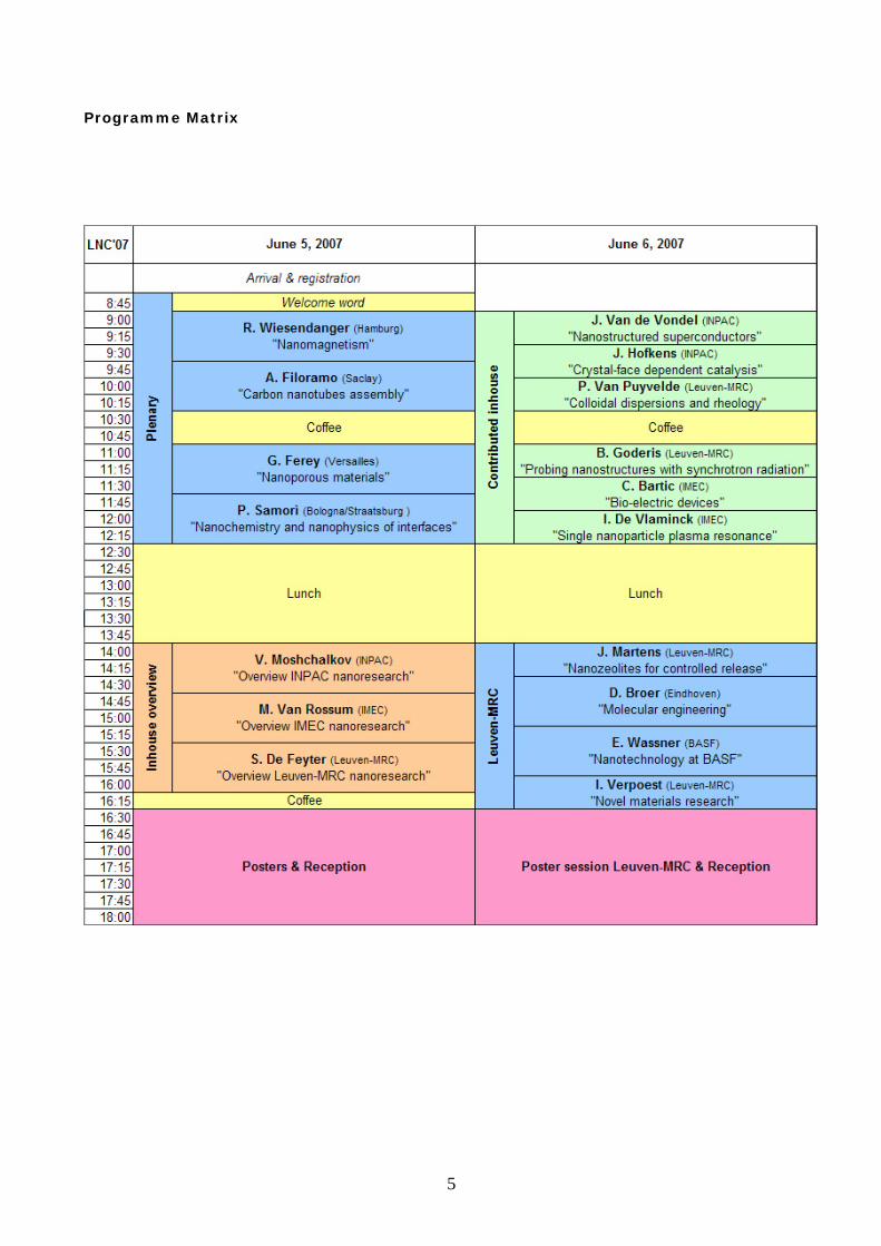
Programme Matrix
6
ORAL PRESENTATIONS
JUNE 5, 2007 Mapping spin structures on the atomic scale. 8 R. Wiesendanger Self assembly approaches for nanoelectronics 9 Arianna Filoramo Metal-Organic Frameworks : the promising young child of the family 10 of porous solids. G. Ferey Hierarchical self-assembly of carbon-based 2D architectures: 11 processing, nanomanipulation and functions P. Samorì Overview INPAC nanoresearch 12 V. Moshchalkov Nanoelectronics at IMEC: Beyond Moore’s law 13 M. Van Rossum Overview Leuven-MRC nanoresearch 14 S. De Feyter

7
ORAL PRESENTATIONS
JUNE 6, 2007 Controlled multiple reversals of the vortex ratchet effect 15 in nanostructured superconductors J. Van de Vondel Single molecule catalysis 16 J. Hofkens Colloidal dispersions and rheology 17 P. Van Puyvelde Probing nanostructures with synchrotron radiation 18 B. Goderis Artificial synapses: interfacing nerve cells and electronics 19 at micro- and nanoscale C. Bartic Optical Near-Field Interactions in Nanomechanics and Plasmonics 20 I. De Vlaminck Development of silica excipient materials for immediate 21 and controlled release Johan Martens Gradient enhanced phenomena in thin polymer films 22 Dirk J. Broer Nanotechnology at BASF: Improved products, 23 more efficient processes and new properties E. Wassner Novel materials research 24 I. Verpoest

8
Mapping spin structures on the atomic scale. R. Wiesendanger Institute of Applied Physics, University of Hamburg, D-20355 Hamburg, Germany [email protected], www.nanoscience.de A fundamental understanding of magnetic and spin-dependent phenomena requires the determination of spin structures and spin excitations down to the atomic scale. The direct visualization of atomic-scale spin structures [1-4] has first been accomplished for magnetic metals by combining the atomic resolution capability of Scanning Tunnelling Microscopy (STM) with spin sensitivity, based on vacuum tunnelling of spin-polarized electrons [5]. The resulting technique, Spin-Polarized Scanning Tunnelling Microscopy (SP-STM), nowadays provides unprecedented insight into collinear and non-collinear spin structures at surfaces of magnetic nanostructures and has already led to the discovery of new types of magnetic order at the nanoscale [6,7]. More recently, the detection of spin-dependent exchange and correlation forces has allowed a first direct real-space observation of spin structures at surfaces of antiferromagnetic insulators [8]. This new type of scanning probe microscopy, called Magnetic Exchange Force Microscopy (MExFM), provides a powerful new tool to investigate different types of spin-spin interactions based on direct-, super-, or RKKY-type exchange down to the atomic level. By combining SP-STM with inelastic electron tunnelling spectroscopy or by performing MExFM together with high-precision measurements of damping forces localized or confined spin excitations in magnetic systems of reduced dimensions now become experimentally accessible. [1] R. Wiesendanger, I. V. Shvets, D. Bürgler, G. Tarrach, H.-J. Güntherodt, J. M. D. Coey, and S. Gräser, Science 255, 583 (1992); R. Wiesendanger, I. V. Shvets, D. Bürgler, G. Tarrach, G. Güntherodt, H.-J. Güntherodt, and J. M. D. Coey, Europhys. Lett. 19, 141 (1992) [2] S. Heinze, M. Bode, O. Pietzsch, A. Kubetzka, X. Nie, S. Blügel, and R. Wiesendanger, Science 288, 1805 (2000) [3] A. Kubetzka, P. Ferriani, M. Bode, S. Heinze, G. Bihlmayer, K. von Bergmann, O. Pietzsch, S. Blügel, and R. Wiesendanger, Phys. Rev. Lett. 94, 087204 (2005) [4] M. Bode, E. Y. Vedmedenko, K. von Bergmann, A. Kubetzka, P. Ferriani, S. Heinze, and R. Wiesendanger, Nature Materials 5, 477 (2006) [5] R. Wiesendanger, H.-J. Güntherodt, G. Güntherordt, R. J. Gambino, and R. Ruf, Phys. Rev. Lett. 65, 247 (1990) [6] K. von Bergmann, S. Heinze, M. Bode, E. Y. Vedmedenko, G. Bihlmayer, S. Blügel, and R. Wiesendanger, Phys. Rev. Lett. 96, 167203 (2006) [7] M. Bode, M. Heide, K. von Bergmann, P. Ferriani, S. Heinze, G. Bihlmayer, A. Kubetzka, O. Pietzsch, S. Blügel, and R. Wiesendanger, Nature (in press) [8] U. Kaiser, A. Schwarz, and R. Wiesendanger, Nature 446, 522 (2007)
9
Self assembly approaches for nanoelectronics Arianna Filoramo Laboratoire d’Electronique Moleculaire, SPEC/DRECAM/DSM, CEA Saclay 91191 Gif Sur Yvette – France The Silicon-CMOS technology is the base of present hardware technology for information processing. Until now, its evolution is governed by the Moore’ laws (1970s), stating that microprocessor performance (defined as the number of transistors on a chip) doubles every 18 months. However, the International Technology Roadmap for Semiconductors (ITRS) [1] predicts that the present CMOS technology will reach its fundamental limits in terms of miniaturisation by 2010-2015, concurrently with a dramatic increase of the cost of the production units. This prompts to study and develop alternative nanofabrication technologies, which will enable the production and manipulation of well-defined structures at the nanoscale level. Indeed, it is well accepted that conventional technologies based on the "top-down” approach are foreseen to experiment difficulties. This is due to the existence of various physical effects that do not down-scale properly, and, most important, to the fabrication cost issues at the nanoscale dimension. At this scale self-assembly, and more generally, “bottom-up” approaches appear to be a more reasonable way to assemble nano-objects into circuits with a two-dimensional and/or three-dimensional layout. In particular, self-assembly is also identified as the most promising way to reduce significantly the fabrication costs compared to what is expected for standard “top-down“ silicon based devices. Indeed, the basic idea of self-assembly is to use a process involving the spontaneous self-ordering of substructures into superstructures. This spontaneous self-ordering is due to specific chemical or physical properties of matter, and relies on the natural tendency of the system to search for a stable configuration. This lecture is not meant to be an exhaustive review of all self-assembly techniques, but rather a focused discussion on the application of this concept to a particular nano-object: carbon nanotube (CNT or NT). At present there are several materials with a potential for the fabrication of a new generation of nanodevices. They vary from conventional semiconductors to conjugated molecules, but among them carbon nanotubes are one of the most interesting. Among the self-assembly methods, we will focus on the methods that permit to localize CNT onto a surface. We will present their advantages, drawbacks and perspectives. In particular, we will discuss in details the DNA-directed approach. This bio-directed method constitutes a genuine and complete molecular-scale bottom-up method, since it relies on recognition properties inherent to biological entities and can be employed without using any standard lithography technique. [1] http://www.itrs.net Dr. Arianna Filoramo, [email protected]

10
Metal-Organic Frameworks : the promising young child of the family of porous solids. G. Férey Institut Lavoisier (UMR CNRS 8180), Université Versailles-St-Quentin en Yvelines, 45, Avenue des Etats-Unis. 78035. VERSAILLES (France). E-mail : [email protected] Metal-Organic Frameworks (MOFs) correspond to a new class of porous solids. Their skeleton combines organic and inorganic moieities linked by strong bonds. Even if they are not conceptually different from the other classes of micro- and mesoporous solids, they present many advantages, some of them unprecedented, which are mainly due to the variability of the organic and inorganic parts which lead to a quasi-infinite number of combinations for the micro- and mesoporous resulting solids, with some spectacular results in terms of specific surfaces (ca. 6000 m2/g) and pore volumes (20,000). The first part of the lecture will focus on the synthesis aspects and the parameters which influence the structures of the final solids, with some details on the richness of the tools like highthroughput and microwave synthesis. Current trends on some specific syntheses will be presented. The second part will be devoted to the structural aspects of MOFs, their description and the building rules which allow a classification of the known structures. Under some conditions, these rules can serve as a good tool for anticipating new solids with a given topology. Beside the numerous rigid structures of MOFs, one feature, specific to MOFs, will be evoked. It concerns dynamic frameworks and large breathing effects and the reasons of such a behaviour. Finally, it will be shown that the combination of targetted chemistry and computer simulation can provide a real prediction of the structures of MOFs, the framework being rigid or not (AASBU method)1. The last part of the lecture will concern the various applications of MOFs. Beside those which are common to the other classes of porous solids (catalysis, separation/sqtorage, catalysis), MOFs exhibit original properties, described in detail in the lecture : long range magnetic interactions, mixed ionic-electronic conduction, high yield luminescence properties, nanosciences, long time delivery of large amounts of drugs. 1. G. Férey, C. Mellot-Draznieks, C. Serre, F. Millange. Acc. Chem. Res. 2005, 38, 217

11
Hierarchical self-assembly of carbon-based 2D architectures: processing, nanomanipulation and functions P. Samorì a Istituto per la Sintesi Organica e la Fotoreattività, Consiglio Nazionale delle Ricerche, via Gobetti 101, I-40129 Bologna (Italy), [email protected] b Institut de Science et d'Ingénierie Supramoléculaires (ISIS), Université Louis Pasteur, 8 allée Gaspard Monge, F-67083 Strasbourg (France), [email protected] Scanning Probe Microscopies (SPMs) are unique tools which make it possible to unravel different physico-chemical properties of supramolecular architectures across multiple length scales, thus they can provide crucial information for the optimization of multifunctional materials for nanotechnology. My lecture will review recent progress in the use of SPMs beyond imaging on soft materials,[1] with a particular emphasis on the Atomic Force Microscopy studies of mechanical properties of isolated polymer chains rigidified by non-covalent interactions.[2] In addition Kelvin Probe Force Microscopy (KPFM) [3] investigations were carried out in order to explore the electronic properties of single [4] and multi-component functional nanostructures. Moreover KPFM made it possible to map the photovoltaic activity in electron acceptor/donor blends both on the hundreds of nanometers [5a] and on the few nanometers scale.[5b] On the other hand, Scanning Tunnelling Microscopy (STM) provided direct insight into the perturbation of the electronic states of molecules adsorbed at surfaces. Detailed understanding on the contrast in sub-molecularly resolved STM images of a monolayer of an azatriphenylene physisorbed on graphite was accomplished relying on the assistance of quantum chemical calculations.[6] I will also present a strategy to fabricate prototypes of mechano-chemical switches triggered by light irradiation: Significantly, the photochemical isomerization of a new terminally thiolated azobiphenyl rigid rod, forming a single component SAM on metallic surfaces, was found by STM to highly cooperative and to be complete over a molecular 2D crystal. [7] Furthermore, the processing of nanomaterials with non-conventional protocols to obtain ordered multifunctional architectures is of key technological relevance. I will introduce three approaches we recently developed in our lab. First, millimetre long crystalline fibers of an organic semiconductor, i.e. perylene-bis-dicarboximide (PDI), were formed using solution processing assisted by solvent vapour annealing post-treatments to foster long-range molecular re-organization on surfaces. This versatile, cooperative and reversible self-assembly was found to comply with an Avrami type nucleation governed growth. The millimetre long fibers revealed a ten-fold increase in conductivity if compared to the pristine PDI thin layer [8]. Second, electrophoretic approaches were successfully employed to nanomanipulate, on a pre-patterned surface, supramolecularly engineered nanofibers pre-programmed to possess an intrinsic high dipole moment.[9] Third, we devised a new general approach to process giant (macro)molecules into ultra-pure and highly ordered structures at surfaces, which relies on the soft-landing of ions generated by solvent-free matrix assisted laser desorption/ionization (MALDI). [10] Overall, the possibility to develop ultra-pure, well-defined and highly ordered functional supramolecular architectures, combined with the ability of SPM to visualize and manipulate nano-objects on the sub-molecular scale, opens new exciting avenues for the exploration and optimization of smart materials, which may be of interest for the fabrication of future organic electronic nanodevices and sensors. [1] (a) P. Samorí, J. Mater. Chem. 2004, 14, 1353. (b) P. Samorì, Chem. Soc. Rev. 2005, 34, 551-561. (c) Scanning probe microscopies beyond imaging (Guest Editor: P. Samorí) Wiley-VCH (2006). [2] P. Samorí, et al Macromolecules 2002, 35 , 5290-5294 [3] V. Palermo, M. Palma, P. Samorì, Adv. Mater 2006, 18, 145-164. [4] A. Liscio, V. Palermo, D. Gentilini, F. Nolde, K. Müllen, P. Samorì Adv. Funct. Mater. 2006, 16, 1407-1416. [5] (a) V. Palermo, G. Ridolfi, A.M. Talarico, L. Favaretto, G. Barbarella, N. Camaioni, P. Samorì, Adv. Funct Mater. 2007, 17, 472-478. (b) M.B.J. Otten, V. Palermo, A. Liscio, E. Schwartz, P.A.J. de Witte, M.A. Castriciano, M.M. Wienk, R.A.J. Janssen, A.E. Rowan, P. Samorì, R.J.M. Nolte, 2007 submitted [6] M. Palma, J. Levin, V. Lemaur, A. Liscio, V. Palermo, J. Cornil, Y. Geerts, M. Lehmann, P. Samorì, Adv. Mater. 2006, 18, 3313. [7] G. Pace, V. Ferri, C. Grave, M. Elbing, M. Zharnikov, M. Mayor, M.A. Rampi, P. Samorì, 2007 submitted [8] G. De Luca, A. Liscio, P. Maccagnani, F. Nolde, V. Palermo, K. Müllen, P. Samorì, 2007 submitted. [9] L. Sardone, et al Adv. Mater. 2006 18, 1276-1280 [10] H.-J. Räder, A. Rouhanipour, A.M. Talarico, V. Palermo, P. Samorì, K. Müllen, Nat. Mater. 2006, 5, 276.
12
Overview INPAC nanoresearch V. Moshchalkov Institute for Nanoscale Physics and Chemistry, Katholieke Universiteit Leuven Celestijnenlaan 200D, B-3001 Heverlee INPAC – Institute for Nanoscale Physics and Chemistry www.kuleuven.be/INPAC – is one of the Centers of Excellence at the K.U.Leuven formed in November 2005 by nine participating teams from three Departments (V.V. Moshchalkov, A. Ceulemans, M. Van der Auweraer, C. Van Haesendonck, A. Vantomme, K. Clays, P. Lievens, A. Stesmans, J. Vanderleiden). INPAC’s mission is to investigate systematically the effect of nanostructuring and nanoscale confinement of charge, spin and photon on the electrical, magnetic, optical and chemical properties of inorganic, organic and bio-materials in order to reveal the fundamental relation between quantized confined states and physical and chemical properties of these materials. This relation will form the backbone of the new concept of “quantum design” through nanostructuring. The basic idea behind the research is to optimize the confinement pattern and the composition, which eventually would lead to the controlled quantum effects providing the desired physical and chemical properties of nanostructured materials and their superior functionality. A brief overview will be given of the most recent results obtained by the INPAC teams.
13
Nanoelectronics at IMEC: Beyond Moore’s law M. Van Rossum IMEC & KULeuven Moore’s law is still driving most of the current R&D for future CMOS integrated circuits, leading to continuous miniaturization of circuits and components. However, in the nanoelectronics regime transistor scaling no longer automatically results in reduced cost and power. Issues such as power dissipation and process variability are now severely complicating the scaling process. The introduction of new materials and new transistor architectures, together with advanced lithography techniques, are necessary to further shrink transistor dimensions while keeping performance at a satisfactory level. CMOS R&D at IMEC now focuses on the 32nm technology node and beyond. This covers research on new materials (high-k dielectrics, metal gates, low-k interconnects), new device concepts (ultra-shallow junctions, strain engineering, alternative transistor structures) and on new lithography methods. The lithography program reached the headlines in the international press several times because of major progress on immersion lithography and the installation of the world’s first Extreme UV tool. The new 300mm-compatible clean room, inaugurated in 2004, is now fully equipped with front-end-of-line and back-end-of-line equipment. Apart from research on logic, there is also an increasing focus on advanced memory concepts. The whole program is supported by a strong packaging activity. For its research on CMOS-based scaling, IMEC relies on an extensive collaboration with material suppliers, tool suppliers, IC manufacturers and foundries. Together, they constitute a unique worldwide network of R&D partners. At the core of the program, nine world leading IC manufacturers support the entire scope of the CMOS research domain. Eventually - some say within the next 10 years - the physical scaling of CMOS transistors will reach its limits. Research groups all over the world are exploring possible routes beyond CMOS and even beyond silicon to ensure the continued success of the IC industry. In this context, IMEC investigates several alternatives to replace silicon for specific applications. The growth of carbon nanotubes and their use in interconnect technology is being considered, as well spintronics technology for the more distant future. Combination of IC technology with biotechnology is now developing into a promising applications area. Organic electronics R&D will create a new platform for special electronics applications. Special efforts are devoted to nanoelectronics-based approaches of energy problems. Together with some other directions, these various research fields are forming the “More than Moore” domain, in which much hope is placed for the future of the semiconductor industry.

14
Overview Leuven-MRC nanoresearch S. De Feyter The Leuven Materials Research Centre has been created at the end of 2005 as an interfaculty collaborative centre, providing a coordinating link between materials science and technology research groups at the K.U.Leuven. Leuven-MRC brings together a large critical mass in materials research, a unique combination of competence and know-how, an impressive and state-of-the-art infrastructure and wide variety of studied material families, processes and applications. The mission of Leuven-MRC is to enhance the innovative character of the top materials research present at the K.U.Leuven by developing and disseminating a common vision on future materials research coordinating interdisciplinary materials research at and with K.U.Leuven strengthening the interaction with industry through its portal function increasing the visibility of materials research. Leuven-MRC is composed of 19 research groups spread over 3 faculties and 9 different departments. In this contribution, selected examples will be given of its activities in the 'nano'-domain, one of the well-chosen focus themes of multidisciplinary interaction within Leuven-MRC and together with the industry and other research centres.

15
Controlled multiple reversals of the vortex ratchet effect in nanostructured superconductors Joris Van de Vondel, CC. de Souza Silva*, Mathieu Morelle and Victor V. Moshchalkov INPAC-Institute for Nanoscale Physics and Chemistry, K.U.Leuven, Celestijnenlaan 200D, B-3001 Leuven, Belgium *Departamento de Fisica, Universidade Federal de Pernambuco, Cidade Universitaria, 50670-901 Recife-PE, Brazil Nanostructured arrays of artificial vortex traps can be used as a very powerful tool for manipulating equilibrium and dynamical properties of vortex matter in superconductors. Diverse collective effects arise due to the competition between interactions of vortices with each other and with the periodic potential generated by the traps as, for instance, the integer and rational matching peaks observed in the critical current vs. field curves. In this work we focus on an interesting dynamical effect resulting from the interaction between vortices and a lattice of asymmetric pinning sites: the vortex ratchet effect. We have studied this effect in type-II Al films with a periodic array of asymmetric antidots [1]. Our data have revealed clear signatures of collective behaviour in the vortex ratchet effect, such as the enhancement of the rectified voltage near matching fields [2]. Moreover, we found that the direction of the vortex drift undergoes a remarkable series of reversals as the vortex density is increased [3], that is, the actual ratchet direction may be inverted several times by simply changing the magnetic field. The periodicity of the reversals may be controlled by the geometrical parameters of the nanostructured sample. By using a model of repelling particles in a one-dimensional ratchet potential we were able to reproduce these results. Our calculations show that multiple reversals result, in a simple way, from the interplay between the inter-particle interactions and the ratchet potential. These multiple sign reversals provide a new tool for controlling and manipulating the motion of magnetic flux quanta in superconductors. Our findings have a very general character and are also relevant for other ratchet systems of interacting particles, like charged colloidal suspensions in ratchet-like microtubules and ions in the selectivity filter of ion channels in cell membranes in two drift regimes: diluted (single particles) and concentrated (interacting particles). [1] J. Van de Vondel, C.C. de Souza Silva, B. Y. Zhu, M. Morelle and V.V. Moshchalkov, Phys. Rev. Lett. 94, 057003 (2005). [2] C.C. de Souza Silva, J. Van de Vondel, B. Y. Zhu, M. Morelle and V.V. Moshchalkov, Phys. Rev. B, 73, 014503 (2006). [3] C.C. de Souza Silva, J. Van de Vondel, M. Morelle and V.V. Moshchalkov, Nature 440, 651 (2006).

16
Single molecule catalysis Roeffaers, M., Uji-i, H., Sels, B., Jacobs, P. ,De Schryver, F.C., De Vos, D., Hofkens, J. Department of Chemistry, Center of Excellence in Catalysis (CECAT) and Institute for Nanoscale Physics and Chemistry (INPAC), Katholieke Universiteit Leuven, Celestijnenlaan 200F, 3001 Heverlee, Belgium, [email protected] In situ physicochemical studies of working heterogeneous catalysts aim at understanding reactions at the surface of solids. Whereas classical techniques only yield ensemble-averaged values for powders, recent progress in (optical) microscopy allows for studying catalytic process with single molecule sensitivity and with high spatial and temporal resolution. Observing a single molecule removes the usual ensemble average, allowing the exploration of hidden heterogeneity in complex condensed phases as well as direct observation of dynamic changes. For example, the application of scanning tunnelling microscopy has improved insights in gas phase reactions on model surfaces. However, catalysts realistically operate at higher pressures or in condensed phase rather than in vacuum and industrial catalysts are often non conductive polycrystalline powders with a three dimensional structure rather than single crystal faces. In this research fluorescence microscopy is used to image chemical transformation under realistic catalytic conditions on catalytic crystals. Layered double hydroxides1 were chosen as catalyst. This material has a crystal structure related to that of brucite (Mg(OH)2), in which MII/MIII isomorphous substitution in the sheets results in a net positive charge of the layers, which is compensated by anions in the interlayers. This gives the materials anion adsorbing and basic properties, both of them being exploited in their use as catalyst. Ad- and desorption of organic molecules2 and organic transformations at the level of individual catalytic turnovers3 were monitored on these crystals. The measurements provide the first direct evidence on the role of different crystal planes in the catalytic process. The research is also extended to other classes of catalytic crystals. In zeolitic materials for example, the accessibility differences of various crystal faces was directly visualized, and further also the catalytic reactivity inside these crystals was monitored in three dimensions. In summary, these results show the strength of fluorescence microscopy as in situ technique in the study of heterogeneous catalysis. References (1) [MII1-xMIIIx (OH)2]x+[An-x/n•yH2O]x- ; MII, MIII are divalent and trivalent cations, An- is an n-valent anion and x between 0.2 and 0.4. (2) Roeffaers, M.B.J.; Sels, B.F.; Loos, D.; Kohl, C.; Man, K.; Jacobs, PA; Hofkens, J.; De Vos, D.E. ChemPhysChem. 6, 2295-2299 (2005) (3) Roeffaers, M.B.J.; Sels, B.F.; Uji-i, H.; De Schryver, F.C.; Jacobs, PA; De Vos, D.E.; Hofkens, J. Nature. 439, 572-575 (2006)

17
Colloidal dispersions and rheology P. Van Puyvelde and J. Vermant Department of Chemical Engineering, K.U. Leuven. Thermodynamic and mechanical forces control the assembly of colloidal and nano-particles. Synthesis, experiments and theory have been successful in measuring, describing and predicting the phase behavior of model spherical colloids and even nano-particles with tailored interactions [1]. In previous years, the effects of tailoring the interparticle interaction from hard to soft repulsion and the effects of attractive interactions on both the phase behavior and other (e.g. rheological) properties have been studied. In some cases, a predictive understanding of the properties is achieved. For example, phase behavior [2], transport and bulk rheological properties of stabilized dispersions can be readily predicted [3,4]. A key technological challenge in designing nanoparticle based materials is to control their flow properties in order to meet the manifold requirements during processing and application, such as to prevent sagging and sedimentation, to ensure easy handling (mixing, pumping, stirring) and good e.g. coating properties, a well-balanced rheological profile has to be provided and tailored for the particular application under consideration. In the present contribution, the interaction and self-assembly of particles leads to structured fluids, with typical features as an (engineering) yield stress and time-dependent (thixotropic) properties, especially at high particle loadings. Progress has recently been made in predicting the linear viscoelastic properties in suspensions containing 'simple' spherical nanoparticles (see e.g. [5]), and an understanding of the link between flow-induced structure and flow properties in suspensions composed of spherical nanoparticles has been developed over the past few years [6] and the issues and outstanding research challenges will be discussed. Flow also can be used as a 'directing field'. The effect of flow on ordering and structuring of nanoparticles needs to be understood for optical or barrier properties to be controlled. In this respect, the effects of changing the nature of the suspending medium to a viscoelastic one can be specifically be exploited. Recent work on colloidal spheres reveal a subtle effect of the rheological medium on chain formation of particles, for non-spherical particles a complex cascade of orientational transitions is observed [8]. Finally, we will briefly discuss the particle size effects when leaving the 'continuum world' and discuss effects that have recently been reported in literature for particle filled polymer melts which at first sight defy the suspension laws for viscosity and diffusion, as derived by Einstein [9] [1] Dhont J.K.G, An Introduction to Dynamics of Colloids, Elsevier (1999) [2] Yodh AG, Lin KH, Crocker JC, et al. Entropically driven self-assembly and interaction in suspension, Phil. Tran Roy Soc. 359 (1782): 921-937 (2001) [3] Petekidis G, Vlassopoulos D, Pusey PN, Yielding and flow of colloidal glasses, Faraday Discussions 123: 287-302 (2003). [4] Mewis J, Vermant J, Rheology of sterically stabilized dispersions and lattices, Prog. Org. Coat. 40 (1-4): 111-117 (2000) [6] Ramakrishnan S, Zukoski CF, Microstructure and rheology of thermoreversible nanoparticle gels, Langmuir 22 (18): 7833-7842 (2006) [7] H. Hoekstra, J. Vermant, J. Mewis and T. Narayanan, Multi length scale analysis of the microstructure in sticky sphere dispersions during shear flow, Langmuir 21 (24): 11017-11025 (2005) [8] J. Vermant, M.J. Solomon Flow-Induced structure in colloidal suspensions Journal of Physics: condensed matter, 17 (4): R187-R216 (2005). [9] M. E. Mackay, T.T. Dao, A.Tuteja, D.L. Ho, B.Van Horn, H. Kim and C. J. Hawker Nature Materials 2, 762–766 (2003).

18
Probing nanostructures with synchrotron radiation B. Goderis Synchrotron radiation is electromagnetic radiation generated by the acceleration of ultrarelativistic (i.e., moving near the speed of light) charged particles through magnetic fields. This may be achieved artificially by storage rings in a synchrotron, or naturally by fast moving electrons moving through magnetic fields in space. The radiation typically includes infrared, optical, ultraviolet, x-rays. Third-generation synchrotron radiation sources, like e.g. the European Synchrotron Radiation Facility (ESRF) are optimized to produce bright X-rays, which can be used to probe the nanostructure of materials in very short time frames (typically seconds) by exploiting the beam absorption or scattering. In 1988, Belgium was one of the twelve founding members of the ESRF. Since 1990 our yearly financial contribution gives us access right to 3% of the available beam time. Moreover, in addition to these public lines, Flemish researchers have access to the Collaborative Research Group (CRG) beam line "Dubble", which has been funded and built as a result of collaboration between FWO-Vlaanderen and the Dutch NWO. The experimental possibilities at these beam lines are discussed and illustrated with some material science oriented examples.

19
Artificial synapses: interfacing nerve cells and electronics at micro- and nanoscale C. Bartic Bioelectronic Systems Group, IMEC vzw, Kapeldreef 75, Leuven 3001, Belgium Tel.: +32 16 281 904; Fax.: +32 16 281 097; [email protected] Nerve cells and other neuronal tissues use complex signal transduction pathways in order to regulate vital processes as development, differentiation, sensorial perception, memory and cognitive processes. The basic biophysical mechanisms underlying these complex processes involve transport of ions and other chemical messengers at the level of ion channels present in the cell membrane and synapses. Yet the membrane potential serves as primary vehicle for the neuronal operations enabling rapid computations in the brain. Hybrid bio-electronic systems allowing us to interact with the electrical and chemical activity of nervous system components will provide powerful tools for the elucidation of neuronal communication mechanisms. Although still in early infancy, neuron-electronic interfaces are already present in retina and cochlear implants and they can, in the future, be used to help brain disorders such Parkinson and Alzheimer diseases. In such systems, we deal with a complex interfacing problem between the biological and hardware components as well as between the micro- and the nano-scale components of the system. The purpose of this lecture is to give an overview of the fundamental aspects involved in the interfacing of individual neurons with electronic devices and the steps that can be taken at micro- and nano- levels towards the connection of silicon chips with living neuronal networks.

20
Optical Near-Field Interactions in Nanomechanics and Plasmonics I. De Vlaminck a), P. Van Dorpe a), J. Roels b), D. Taillaert b), D. Van Thourhout b), R. Baets
b), L. Lagae a), G. Borghs a) a) IMEC, Kapeldreef 75, 3000, Leuven, Belgium b) Ghent Univeristy-IMEC (INTEC In order to exploit the full potential of nanotechnology in creating systems with great functional density and diversity, techniques that allow local communication with nanoscale components are highly desirable. In this talk, we will demonstrate how optical near-field interactions can be exploited for efficient transduction of both mechanical motion of nanoscale resonators and plasmonic excitations in metallic nanoparticles. A central problem in the development of mechanical devices and systems is accurate and fast motion sensing. We demonstrate that this problem can be solved by fabricating a mechanical device in close proximity of a photonic waveguide [1]. Through a process of photon tunneling, optical energy in the guided mode of the photonic waveguide can couple to the nanomechanical structure. Exploiting the strong dependence of this coupling to changes in separation between the waveguide and the mechanical resonator we were able to detect in- and out-of-plane displacements. We conclude this part of the presentation with a discussion of possible applications. In the second part of the talk we apply a similar idea to the transduction of Localized Surface Plasmon resonances in metallic nanostructures. Surface Plasmons are electromagnetic excitations existing at the surface of metals or in metal nanostructures. The properties of surface plasmons have received great interest in recent years as it is recognized that they have the ability to overcome the size-mismatch between diffraction limited photonic components and nanoscale objects, opening up new possibilities in, e.g. optical signal processing and biosensing. Through optical near-field coupling of a metal nanoparticle to a nanoscale semiconducting photodetector we were able to detect plasmonic resonances of individual nanostructures. In this talk we will highlight our current efforts in integrating these devices with fluidic components to create a biosensing system and discuss opportunities in fast signal processing and optical communication. [1] I. De Vlaminck, J. Roels, D. Taillaert, D. Van Thourhout, L. Lagae, R. Baets, G. Borghs “Sensitive detection of nanomechanical motion through evanescent light-wave coupling” Applied Physics Letters, submitted (2006). [2] I. De Vlaminck, P. Van Dorpe, L. Lagae, G. Borghs “Local electrical detection of single nanoparticle plasmon resonance” Nano Letters, 7, 703 (2007).
21
Development of silica excipient materials for immediate and controlled release Randy Mellaerts1, Caroline Aerts1, Johan Martens1, Jan Van Humbeeck2, Patrick Augustijns3 and Guy Van den Mooter3 1, Centre of Excellence in Catalytic Science; 2, Afdeling fysische materiaalkunde, Departement MTM; 3, Laboratorium voor Farmacotechnologie en biofarmacie, KU Leuven. Drug formulation is an important aspect of pharmaceutical research. Especially the formulation of poorly soluble drug compounds can be problematic and can present a serious obstacle for newly discovered drug compounds to come to application. Among the possible approaches the development of excipient materials is an attractive option. The interest of the pharmaceutical research community in silica excipient materials as a means of release control is growing rapidly. Silica is non toxic and is known for its excellent biocompatibility. In this presentation two new types of silica excipients are presented. With the advent of ordered mesoporous silica materials new tools to construct drug delivery carriers became available. Originally, the focus of mesoporous silica materials has been on the development of slow release formulations. We demonstrate that the presence of a sufficiently wide pore diameter is the key for accelerating the release of the poorly soluble drugs such as itraconazole. The rapid release kinetics can be explained by a displacement desorption of itraconazole caused by influx of water. The hydrophilicity of the silica pore walls is such that adsorbed itraconazole molecules are lifted from the surface by competitive adsorption with water molecules and exported to the surrounding medium (Scheme 1). Amorphous microporous silica (AMS) materials with subtle variation of porosity were prepared using an acid-catalyzed sol-gel process departing from tetraethylorthosilicate. Molecules such as ibuprofen can be molecularly dispersed in the AMS micropores. In vitro buprofen release from AMS was investigated in simulated intestinal fluid and in a dissolution medium simulating the gastrointestinal tract with simulated gastric fluid followed by simulated intestinal fluid. AMS has particular advantages in the controlled release application. Drug release from the silica particles is controlled by configurational diffusion. The diffusion constant can be varied by orders of magnitude by adapting the pore diameter. AMS xerogel can be fined to different particle sizes by crushing and sieving. Ibuprofen release kinetics from AMS can be fine tuned by adjusting AMS pore diameter and particle size.
22
Gradient enhanced phenomena in thin polymer films Dirk J. Broer Philips Research Laboratories, Eindhoven University of Technology Plastics or polymers are ductile materials that are easy to shape and process. Traditionally they are used as packaging and construction materials. The control over the molecular structure and the way they pack in three dimensional arrangements make them also suited as functional elements in (opto)electronics products and biomedical devices. Liquid crystal technology is a convenient instrument to establish this. We developed special processes based on photo-chemistry, self-organization, well-controlled diffusion induced by localized polymerization and phase separation to control the molecular organization and the formation of structures on (sub) nanometer level. This has led to unique properties, such as diffraction of linearly polarized light, selective reflection of circularly polarized light, or to unique products, such as paintable displays and all-in-one display illumination systems. In addition to the diffusion processes on microscopic scale, the control over the adjusted morphology and molecular orientation profiles over the cross-section of thin patterned films also enables us to create motion in the polymers over macroscopic dimensions. A property that leads to new applications such as thin-film actuators or artificial muscles.
23
Nanotechnology at BASF: Improved products, more efficient processes and new properties E. Wassner BASF Aktiengesellschaft, Polymer Physics Nanotechnology is considered to be one of the most important emerging technologies worldwide. Through the controlled manufacture and structuring of materials, it allows the creation of completely new properties in product development. For BASF, the application of new insights and developments in nanotechnology is a decisive step on the road to profitable growth through innovation. The company intends to spend €180 million in these activities up to 2008. Besides manufacturing nanoparticles and studying their properties, BASF also devotes considerable research effort to the risk assessment of nanoparticles. In this talk, several examples from nanotechnology research at BASF are presented, e.g. Ultradur® High Speed, a nanotechnology-based engineering plastic, that offers numerous advantages, for customers in the automotive and electronics industries. A nanoparticulate additive greatly improves the flowability of the plastic while preserving its mechanical properties. Thanks to their extremely fine nanostructure, BASF's next-generation binders COL.9®, make surfaces particularly resistant to weathering and dirt. The textile finishing Mincor® TXTT contains nanoparticles that provide a self-cleaning effect. Cube-shaped nanostructures known as metal organic frameworks (MOFs) are capable of storing large amounts of energy-rich gases making them suitable for use in automobiles as well as energy sources for electronic devices in the future. Plastic foams with nanodimensional pores reduce the thermal conductivity to one-third of a conventional insulating material. This also benefits the environment because nanofoams reduce energy consumption and also save material.

24
Novel materials research I. Verpoest, K. Van Acker The open annual meeting of the Leuven Materials Research Centre will be concluded with an overview of the activities of Leuven-MRC in the past 12 months and a look ahead to the strategy for the next years. In line with the objectives of Leuven-MRC, a number of new interdisciplinary research projects have been started, new interactions with industrial companies have been set up, and the visibility of the materials research at K.U.Leuven has been enhanced. Internal expert panel discussions about a vision on future materials research at K.U.Leuven have led to the definition of new focussed interdisciplinary research lines, which will be presented at the annual meeting.

25
POSTERS
P.1. Activation of silica materials with anatase towards degradation of organic compounds Koen De Witte, Pegie Cool and Etienne F. Vansant
P.2. Superconducting properties of Ga grains in GaAs Bram Willems, David Taylor, Victor Moshchalkov
P.3. Development of combined micro- / mesoporous material synthesized from zeolite Y precursor solution E. Bruijn, V. Meynen, P. Cool, E. F. Vansant
P.4. Molding Fluorescence by Photonic Band Gap Engineering Branko Kolaric, Kasper Baert, Renaud A. L. Vallée, Mark Van der Auweraer and Koen Clays
P.5. Wiener and Szeged Index of Nanotori Ali Reza Ashrafi and Shahram Yousefi
P.6. Nanowires Arrays Used For Biosensors with High Active Surfaces V. A. Antohe, S. Mátéfi-Tempfli, A. Vlad, D. Serban, M. Mátéfi -Tempfli, S.Melinte, L. Piraux
P.7. Tunable Field Induced Superconductivity W. Gillijns, A.V. Silhanek, V.V. Moshchalkov
P.8. Thermodynamically stable noncomposite vortices in mesoscopic two-gap superconductors L.F. Chibotaru, V.H. Dao, and A. Ceulemans
P.9. Low Temperature Induced Magnetoelastic Anisotropy in Electrodeposited Ni Nanowires Embedded in Polymer Templates Joaquin De La Torre Medina, Michael Darques and Luc Piraux
P.10. Effect of a reduced mobility layer on the interplay between molecular relaxations and diffusion limited crystallization rate in ultrathin polymer films Simone Napolitano, Michael Wübbenhorst
P.11. Controlled growth of single nanowires within supported alumina template: towards circuit integration A. Vlad, M. Mátéfi -Tempfli, S. Faniel, N. Reckinger, A. Crahay, B. Olbrechts, V. Bayot, L. Piraux, S. Melinte and S. Mátéfi -Tempfli
P.12. Scanning Hall probe microscopy of vortex patterns in superconducting micro-squares. Katrien De Keyser, Taichiro Nishio, Roman Kramer, Koen Vervaeke, and Victor V. Moshchalkov
P.13. Order parameter nucleation in superconducting films of finite thickness in presence of nonuniform magnetic field A.Yu. Aladyshkin, D.A. Ryzhov, A.V. Samokhvalov, D.V. Savinov, A.S. Melnikov and V.V. Moshchalkov
P.14. Magnetic Flux penetration patterns in superconductors with asymmetric pinning potentials M. Menghini, J. van de Vondel, G. D. Gheorghe, R. J. Wijngaarden and V. V. Moshchalkov
P.15. Nanoscale thick novel high-k insulator films on silicon: investigation of interface properties M. Badylevich, S. Shamuilia, V. V. Afanas’ev, and A. Stesmans, A. Laha, H. J. Osten, L. F. Edge, W. Tian, D. G. Schlom, J. M. J. Lopes, M. Roeckerath and J. Schubert, Y. Fedorenko, S. De Gendt
P.16. Ru(TAP)32+ photosensitized DNA cleavage studied by atomic force microscopy and gel electrophoresis: a comparative study Hiroshi Uji-i, Philippe Foubert, Willem Vanderlinden, Frans C. De Schryver, Steven De Feyter, Etienne Gicquel, Ariane Etoc, Cécile Moucheron, André Kirsch-De Mesmaeker
P.17. Expression of Molecular Chirality at the Liquid/Solid Interface Hong Xu, Zeljko Tomovic, Andrea Minoia, Albertus P. H. J. Schenning, Roberto Lazzaroni, E. W. Meijer, Steven De Feyter

26
P.18. Magnetoplumbite as a Template for Nucleation of Superconductivity J. Fritzsche, H. Eitel, D. Koelle, R. Kleiner, R. Szymczak, V.V. Moshchalkov
P.19. Defocused imaging of 3D rotation of single molecule in thin polymer films near Tg Hiroshi Uji-i,Ania Deres, Dominik Wüll, Andreas Hermann, Klaus Müllen, Jörg Enderlein, Johan Hofkens
P.20. Self-assembly of an ureidophtalimide based foldamer on graphite Renatus W. Sinkeldam, Freek J. M. Hoeben, Maarten J. Pouderoijen, Inge De Cat, Jian Zhang, Shuhei Furukawa, Steven De Feyter, Jef A. J. M. Vekemans, E. W. Meijer
P.21. High resolution optical microscopy Jun-ichi Hotta, Peter Dedecker, Benoit Muls, Cristina Flors, Michel Sliwa, and Johan Hofkens
P.22. Electroluminescence of smell metal clusters in nanoscale break junctions. Tom Vosch, Johan Hofkens, Robert Dickson, Jose Gonzalez
P.23. Observation of Localized Surface Plasmons on Silver Nanowires by Wide-field Microscopy M. Linh Tran, Silvia P. C. Benigno, Hans Engelkamp, Hiroshi Ujii, Johan Hofkens, Steven De Feyter, and Mark van der Auweraer
P.24. Nanocluster assembled films for hydrogen storage M. Di Vece, P. Lievens
P.25. Unravelling and Guiding the Fibre Formation of a Second Generation Polyphenylene Dendrimer An Ver Heyen, C. C. Buron, A. A. Jonas, K. Müllen, F. C. De Schryver, S. De Feyter
P.26. Voltage rectification effects in superconducting triangles N. Schildermans, R. Salenbien, A. V. Silhanek, and V. V. Moshchalkov
P.27. Stability and dissociation pathways of doped AunX+ clusters (X = Y, Er, Nb): evidence for enhanced stability of 18-electron clusters N. Veldeman, E. Janssens, K. Hansen, J. De Haeck, R.E. Silverans, P. Lievens
P.28. ScCu16+, a stable dopant encapsulated copper cage: Experimental observation and
computational identification Nele Veldeman, Tibor Höltzl, Sven Neukermans, Tamás Veszprémi, Minh Tho Nguyen, and Peter Lievens
P.29. Electronic Structure of Bimetallic Nanoclusters of Germanium and Lithium atoms. Xin WANG, Ewald Janssens, G. Gopakumar, Peter Lievens, Minh Tho Nguyen
P.30. Argon complex formation as a structural probe for endohedral transition metal doped silicon clusters Ewald Janssens, Philipp Grüne, Gerard Meijer, Ludger Wöste, André Fielicke, Peter Lievens
P.31. Scanning probe microscopy of deposited carbon nanotubes and nanowalls M. Pal Chowdhury, A. Volodin, A. Malesivic, A. Vanhulsel, C. Van Haesendonck
P.32. Magnetization Tunnelling in Mn12Ac studied in pulsed magnetic fields Wim Decelle, Johan Vanacken and Victor V. Moshchalkov
P.33. A Compact Synchrotron Light Source for in-situ structural analysis of thin film deposition processes. Jean-Pierre Locquet, Johan Vanacken and Hironari Yamada
P.34. Synchrotron X-ray Powder diffraction and Absorption Spectroscopy in Pulsed Magnetic Fields with Milliseconds Duration J. Vanacken, C. Detlefs, O. Mathon, P. Frings, F. Duc, J.E. Lorenzo, M. Nardone, J. Billette, A. Zitouni, M-C. Dominguez, J. Herczeg, W. Bras, V.V. Moshchalkov and G. Rikken
P.35. Optical properties of molecular and nanomaterials V.K. Valev, S. Fourier, G. Wouters, M.A. Vander Veen, D.E. De Vos, T. Verbiest
P.36. Low-temperature scanning tunneling microscopy and spectroscopy of self-organized nanoscale Co islands on Au(111) K. Schouteden, P. Lievens, and C. Van Haesendonck

27
LIST OF PARTICIPANTS
Lastname Firstname Email Aladyshkin Alexei [email protected] Alaerts Luc [email protected] Alexandru Vlad [email protected] Almeida Francisco [email protected] Antohe Vlad – Andrei [email protected] Arkens Oger [email protected] Arnout Sander [email protected] Ashrafi Ali Reza [email protected] Asselberghs Inge [email protected] Badylevich Mikhail [email protected] Baert Kasper [email protected] Bartic Carmen [email protected] Bonnevie Michel [email protected] Borghs Gustaaf [email protected] Broer Dick [email protected] Bruijn Erik [email protected] Cambier Frederik [email protected] Cano odena Angels [email protected] Carlon Enrico [email protected] Casteele Chris [email protected] Celis Jean-Pierre [email protected] Ceulemans Arnout [email protected] Chen qinghua [email protected] Chibotaru Liviu [email protected] Cottenier Stefaan [email protected] Dao Vu Hung [email protected] De Bruyne Roger [email protected] De Cat Inge [email protected] De Doncker Lieve [email protected] De Feyter Steven [email protected] De Gendt Stefan [email protected] De Keyser Katrien [email protected] De Keyzer René [email protected] De La Torre Medina [email protected] De Meyer Christy [email protected] De Vlaminck Iwijn [email protected] De Witte Koen [email protected] Decelle Wim [email protected] Decoster Stefan [email protected] Di Vece Marcel [email protected] Drees Dirk [email protected] Ferey Gérard [email protected] Flors Cristina [email protected] Foerier Stijn [email protected] Follens Lana [email protected] Franz Edith [email protected] Fritzsche Joachim [email protected] Geeraert Jan [email protected] Gillijns Werner [email protected] Gladilin Vladimir [email protected] Goderis Bart [email protected] Gopinadhanpillai Gopakumar [email protected] Groeninckx Gabriel [email protected] Herlach Fritz [email protected] Heymans Luc [email protected] Hillaert Rik [email protected]

28
Hofkens Johan [email protected] Holtzl Tibor [email protected] Hotta Jun-ichi [email protected] Iacopi Francesca [email protected] Kolaric Branko [email protected] Kramer Roman [email protected] Kumar Rohit [email protected] Kuypers Stefan [email protected] Laenens Bart [email protected] Langenbick Johan [email protected] Lievens Peter [email protected] Lijnen Erwin [email protected] Locquet Jean-Pierre [email protected] Lomov Stepan [email protected] Luyten Walter [email protected] Martens Johan [email protected] Melotte Joseph [email protected] Meneve Jan [email protected] Menghini Mariela [email protected] Mertens Robert Pierre [email protected] Mercier Jean P. [email protected] Moldenaers Paula [email protected] Moshchalkov Victor [email protected] Naelaerts Ludo [email protected] Napolitano Simone [email protected] Nguyen Vinh Son [email protected] Nishio Taichiro [email protected] Nuytten Thomas [email protected] Pal Chowdhury Manish [email protected] Parshin Mikhail [email protected] Qian Jun [email protected] Ramaekers Peter [email protected] Salehi Arezou [email protected] Samori Paolo [email protected] Sarkar Pal Sudipta [email protected] Saurel Damien [email protected] Schildermans Nele [email protected] Sijnave Jan [email protected] Silhanek Alejandro [email protected] Smeets Dries [email protected] Snauwaert Johan [email protected] Soncini Alessandro [email protected] Steenhaut Oscar [email protected] Stesmans Andre [email protected] Stiens Johan [email protected] Stuyven Bernard [email protected] Tandon Nandan [email protected] Taylor David [email protected] Temst Kristiaan [email protected] Tran Linh [email protected] Ujii Hiroshi [email protected] Ustinov Konstantin [email protected] Valev Ventsislav [email protected] Van Acker Karel [email protected] Van Aken Lucas [email protected] Van Bael Margriet [email protected] Van Cleuvenbergen Stijn [email protected] Van de Sande Christian [email protected] Van de Vondel Joris [email protected] Van der Auweraer Mark [email protected] Van der Burght Els [email protected]
29
van der Veen Monique [email protected] van der Velden Peter [email protected] Van Noyen Jasper [email protected] Van Puyvelde Peter [email protected] Van Rossum Marc [email protected] Van Stappen Marc [email protected] van Vuure Aart [email protected] Vanacken Johan [email protected] Vanderlinden Willem [email protected] Vantomme Andre [email protected] Ver Heyen An [email protected] Verbiest Thierry [email protected] Verellen Niels [email protected] Verlinden Bert [email protected] Verpoest Ignace [email protected] Vervaeke Koen [email protected] Vleugels Jozef [email protected] Volodin Alexander [email protected] Vosch Tom [email protected] Vu Thi Ngan [email protected] Vu Thi Thuy [email protected] Wang Huan [email protected] Wassner Erik [email protected] Wevers Martine [email protected] Wiesendanger Roland [email protected] Willems Bram [email protected] Wouters Jelle [email protected] Xu Hong [email protected] Zhan Qingfeng [email protected] Zhao Qiang [email protected] Zutterman Freddy [email protected]