Embed Size (px)
Citation preview
Design and Analysis of SRAMs for
Energy Harvesting Systems
By
Abdullah Baz
School of Electrical, Electronic and Computer Engineering
Newcastle University
A thesis submitted in fulfilment of the requirements for the
degree of Doctor of Philosophy
April 2014
I
Abstract
At present, the battery is employed as a power source for wide varieties of
microelectronic systems ranging from biomedical implants and sensor net-
works to portable devices. However, the battery has several limitations and
incurs many challenges for the majority of these systems. For instance, the
design considerations of implantable devices concern about the battery from
two aspects, the toxic materials it contains and its lifetime since replacing
the battery means a surgical operation. Another challenge appears in wire-
less sensor networks, where hundreds or thousands of nodes are scattered
around the monitored environment and the battery of each node should be
maintained and replaced regularly, nonetheless, the batteries in these nodes
do not all run out at the same time.
Since the introduction of portable systems, the area of low power designs
has witnessed extensive research, driven by the industrial needs, towards
the aim of extending the lives of batteries. Coincidentally, the continuing
innovations in the field of micro-generators made their outputs in the same
range of several portable applications. This overlap creates a clear oppor-
tunity to develop new generations of electronic systems that can be powered,
or at least augmented, by energy harvesters. Such self-powered systems
benefit applications where maintaining and replacing batteries are impossi-
ble, inconvenient, costly, or hazardous, in addition to decreasing the adverse
effects the battery has on the environment.
The main goal of this research study is to investigate energy harvesting
aware design techniques for computational logic in order to enable the capa-
II
bility of working under non-deterministic energy sources. As a case study,
the research concentrates on a vital part of all computational loads, SRAM,
which occupies more than 90% of the chip area according to the ITRS re-
ports.
Essentially, this research conducted experiments to find out the design met-
ric of an SRAM that is the most vulnerable to unpredictable energy sources,
which has been confirmed to be the timing. Accordingly, the study proposed
a truly self-timed SRAM that is realized based on complete handshaking
protocols in the 6T bit-cell regulated by a fully Speed Independent (SI) tim-
ing circuitry. The study proved the functionality of the proposed design in
real silicon. Finally, the project enhanced other performance metrics of the
self-timed SRAM concentrating on the bit-line length and the minimum op-
erational voltage by employing several additional design techniques.
III
Preface
The results in this PhD thesis are realized within the framework of the pro-
ject “Next Generation Energy harvesting Electronics: A Holistic Approach”,
which is a £1.6M project funded by EPSRC. The project involves four uni-
versities, namely, the University of Southampton, Newcastle University,
Imperial College, and the University of Bristol. All academic institutions are
undertaking the three-year collaborative research project in partnership
with four industrial companies: Dialog Semiconductor, Diodes Incorporated,
ARM, and Mentor Graphics.
More information can be found in the project website:
http://www.holistic.ecs.soton.ac.uk/index.php
IV
Acknowledgments
Since November 2009, I have been a research student with the Holistic pro-
ject and currently, I am approaching the end of my third PhD year. During
this time, I have fabricated three chips, published four papers in interna-
tional conferences, an invited journal paper, and several more are being
prepared for submission. The results obtained throughout the study period
were realized by developing several program codes, mastering different
EDA/CAD tools, and testing numerous hardware components, equipment,
and boards in the laboratory. Certainly, carrying out all this work alone is
difficult if not impossible. Accordingly, it is the aim of this text to
acknowledge those key people, without their invaluable help, the mentioned
achievements would not be possible.
First of all, I wish to express my extreme gratitude to my research supervi-
sor Professor Alex Yakovlev for his incredibly wise guidance and motiva-
tions during my research. I appreciate his support for attending all training
courses, meetings, and conferences I have requested throughout my study. I
owe him special thanks for sponsoring me to fabricate three chips while very
few supervisors around the world do that.
Next, my sincere thanks go to Dr. Delong Shang, my colleague and mentor,
for his help throughout this research. He always had the time to propose
new ideas to me and discuss my results.
In addition, I acknowledge the efforts that my colleague, Mr. Reza Rameza-
ni, has made to complete part of the digital part of my first SRAM chip. Fol-

V
lowing my first chip, I helped him in designing the full-custom and analogue
part of his sensor chip. I really enjoyed that collaborative work.
The same thanks go to my friend, Mr. Xuefu Zhang, who has successfully
designed and fabricated his novel power delivery method, coined Capacitor
Bank Block (CBB). His portable demonstration box was controlled by mine
to prove the functionality of the SRAM in several venues including
PATMOS 2012 in Newcastle, the final advisory board meeting of holistic
project in the University of Southampton, the final project showcase held in
Imperial College, the 3rd annual Energy harvesting conference in London,
and the Async 2013 conference in Santa Monica.
Most importantly, Umm Al-Qura University, the Ministry of Higher Educa-
tion in the Kingdom of Saudi Arabia, and the Saudi Cultural Bureau in
London have financially supported my study as well as my living expenses
in the UK. Definitely, without their support the aforementioned achieve-
ments would not have been possible, my sincere thanks go to them.
Above and beyond all else, my parents, my first teachers in this life, have
been continuously supporting and encouraging me throughout my study as
well as my life. Without their incredibly wise guidance, such a level would
never be reached and such a work would never be achieved. Despite that I
lost my father in the second year of my PhD, he still inspires me to reach
ever further.
Next in importance, I express my special and sincere thanks and extreme
gratitude to my wife, son, and daughter for their love, support, and patience
throughout my study. I really appreciate the time they sacrificed to allow
me progress more.
Finally, I apologize in advance, to those I might have forgotten to mention.
VI
Contents
Abstract .......................................................................................................................................... I
Preface ......................................................................................................................................... III
Acknowledgments ........................................................................................................................ IV
Contents ....................................................................................................................................... VI
List of Tables ................................................................................................................................ IX
List of Figures ................................................................................................................................ X
Chapter 1. Introduction ................................................................................................................ 1
1.1 Introduction ........................................................................................................................ 1
1.2 Motivation ........................................................................................................................... 3
1.3 Research Originality and Contributions .............................................................................. 5
1.4 Research Management and Involved Risks ........................................................................ 7
1.5 Thesis Outline and Achievements ....................................................................................... 7
1.6 Publications ......................................................................................................................... 8
1.7 References .......................................................................................................................... 9
Chapter 2. Background ............................................................................................................... 11
2.1 Introduction ...................................................................................................................... 11
2.2 Energy Harvesting Systems: Next Generation of Microelectronics .................................. 11
2.2.1 Micro Generators ....................................................................................................... 12
2.2.2 Energy Harvesting Electronics .................................................................................... 17
2.3 SRAM ................................................................................................................................. 18
2.3.1 SRAM Structure and Operational States .................................................................... 18
2.3.1.1 Holding State ....................................................................................................... 19
2.3.1.2 Reading State ...................................................................................................... 21
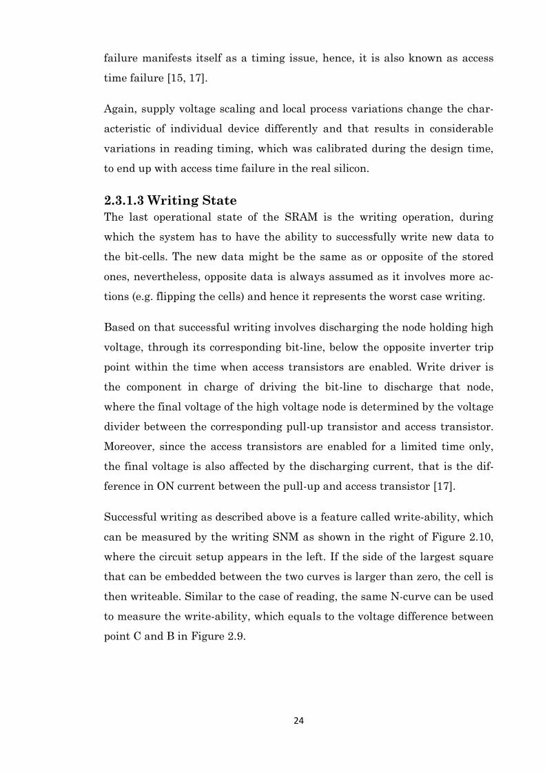
2.3.1.3 Writing State ....................................................................................................... 24
2.3.2 SRAM Design Challenges ............................................................................................ 25
2.3.3 SRAM Design Approaches .......................................................................................... 29
VII
2.3.3.1 Bit-Cell Based Techniques ................................................................................... 30
2.3.3.2 Voltage Level Based Techniques ......................................................................... 34
2.3.3.3 Timing Circuit Based Techniques ........................................................................ 38
2.3.3.4 Peripheral Circuit Based Techniques .................................................................. 40
2.4 Summary ........................................................................................................................... 40
2.5 References ........................................................................................................................ 41
Chapter 3. Truly Self-Timed SRAM .............................................................................................. 46
3.1 Introduction ...................................................................................................................... 46
3.2 Problem Statement: Timing Variations in Non-Deterministic Environments ................... 46
3.2.1 SRAM Latency under Different VDDs ......................................................................... 47
3.3 Methodology and Design Strategy: Power Adaptive Computing ..................................... 49
3.3.1 Self-Timed SRAM ........................................................................................................ 50
3.4 Investigations on the Proposed SI SRAM .......................................................................... 55
3.4.1 Behaviour of SI SRAM under Variable VDD ................................................................ 56
3.4.2 Timing and Energy Computations .............................................................................. 57
3.4.3 Energy Overhead ........................................................................................................ 59
3.5 More Efficient Design Technique: Smart Latency Bundled Self-Timed SRAM .................. 60
3.5.1 Bundling Techniques in Self-Timed SRAM ................................................................. 61
3.5.2 Timing and Energy Comparisons ................................................................................ 66
3.6 Conclusion ......................................................................................................................... 69
3.7 References ........................................................................................................................ 71
Chapter 4. Design, Fabrication and Testing of HoliSRAM ........................................................... 73
4.1 Introduction ...................................................................................................................... 73
4.2 Chip Architecture .............................................................................................................. 73
4.2.1 Dual Power Domain Design Phase ............................................................................. 78
4.2.2 Dual Cell Design Phase ............................................................................................... 80
4.3 Chip Design Flow ............................................................................................................... 81
4.3.1 Results of Chip Simulation ......................................................................................... 81
4.4 Chip Testing ....................................................................................................................... 85
4.4.1 Stream II Demonstration: a Portable HoliSRAM Box ................................................. 85
4.4.2 Interactive Interface for Interactive Demonstration ................................................. 90
4.4.3 Measurements and Testing Results ........................................................................... 91
4.5 Conclusions ....................................................................................................................... 96
4.6 References ........................................................................................................................ 97
Chapter 5. Improving the Robustness of Self-Timed SRAM ....................................................... 98
VIII
5.1 Introduction ...................................................................................................................... 98
5.2 Preliminary Analysis .......................................................................................................... 98
5.3 New Robust Self-Timed SRAM: a Bit-Cell Based Technique ........................................... 101
5.3.1 Investigations on the Proposed Bit-Cell Based Technique ...................................... 104
5.4 Bit-line Keeper: a Peripheral Circuit Based Technique ................................................... 106
5.4.1 Investigations on the Proposed Peripheral Circuit Based Technique ...................... 107
5.5 Virtual Ground: a Voltage Level Based Technique .......................................................... 110
5.5.1 Investigations on the Proposed Voltage Level Based Technique ............................ 113
5.6 Conclusions ..................................................................................................................... 114
5.7 References ...................................................................................................................... 116
Chapter 6. Conclusions and Future Work ................................................................................. 117
6.1 Introduction .................................................................................................................... 117
6.2 View and Review ............................................................................................................. 117
6.3 Prospective Future Research .......................................................................................... 121
6.4 References ...................................................................................................................... 123
Appendix A. Hardware Supplements ........................................................................................ 124
A.1 Tool Path ......................................................................................................................... 124
A.2 Introduction .................................................................................................................... 127
A.3 Chip Gallery ..................................................................................................................... 127
A.4 Demonstration PCB ........................................................................................................ 128
A.5 PIC32 Interface Code ...................................................................................................... 134
IX
List of Tables
Table 2.1 Amount of power that can be harvested from different ambient energy sources. ... 12
Table 2.2 Comparisons between transduction mechanisms of vibration energy harvesters .... 14
Table 2.3 Scaling parameters. ..................................................................................................... 25
Table 4.1 Functional yield of the SI SRAM. ................................................................................. 84
Table 4.2 Components list of the portable demonstration box. ................................................ 89
Table 4.3 µC ports employed during the demonstration. .......................................................... 90
Table 6.1 Comparison between the designs proposed in the thesis ........................................ 120 Table A.1 Chip Gallery ............................................................................................................... 128
X
List of Figures
Figure 2.1 Electromagnetic transduction technique. ................................................................. 13
Figure 2.2 Piezoelectric transduction technique. ....................................................................... 13
Figure 2.3 Two different configurations for electrostatic transduction technique. ................... 14
Figure 2.4 Schematic of thermocouple and of a thermopile. ..................................................... 15
Figure 2.5 Cross coupled inverters with two voltage sources to model static noise. ................ 19
Figure 2.6 Basic SRAM system block diagram. ............................................................................ 20
Figure 2.7 Butterfly curves of the 6T cell during holding state. .................................................. 21
Figure 2.8 Butterfly curves of the 6T cell during reading............................................................ 22
Figure 2.9 The schematic used to extract the N-curve and the resulted N-curve. ..................... 23
Figure 2.10 The schematic used to extract the WSNM together with the extracted curves. .... 25
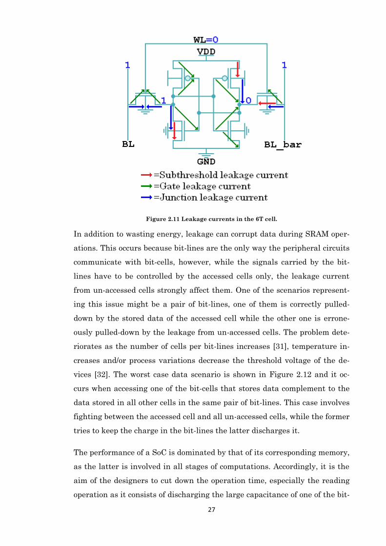
Figure 2.11 Leakage currents in the 6T cell. ............................................................................... 27
Figure 2.12 Worst case data scenario for bit-line leakage.......................................................... 28
Figure 2.13 Published SRAM bit-cells.......................................................................................... 31
Figure 3.1 A method to investigate timing discrepancy between SRAM and inverter chain. .... 48
Figure 3.2 Timing mismatch between SRAM and its bundling delay element. .......................... 48
Figure 3.3 Block diagram of the proposed self-timed memory system. ..................................... 52
Figure 3.4 STG specifications of the reading and writing operations in the 6T cell.................... 53
Figure 3.5 Possible implementation of the STG’s in Figure 3.4. ................................................. 54
Figure 3.6 Critical waveforms of self-timed SRAM under variable VDD. .................................... 56
Figure 3.7 Operation delay of the proposed self-timed SRAM. .................................................. 58
Figure 3.8 Energy consumptions of the proposed self-timed SRAM. ......................................... 58
Figure 3.9 Energy overhead of the proposed timing controller during writing. ......................... 59
Figure 3.10 Energy overhead of the proposed timing controller during reading. ...................... 60
Figure 3.11 Bundling scheme in self-timed SRAM. ..................................................................... 61
Figure 3.12 Modified writing STG for latency bundled SRAM. ................................................... 64
Figure 3.13 Modified timing circuit based on the modified STG. ............................................... 66
Figure 3.14 Writing latency comparison between fully SI and smartly bundled SRAM. ............ 68
Figure 3.15 Reading latency comparison between fully SI and smartly bundled SRAM. ........... 68
Figure 3.16 Writing energy comparison between fully SI and smartly bundled SRAM. ............. 69
Figure 3.17 Reading energy comparison between fully SI and smartly bundled SRAM. ............ 69
Figure 4.1 Main part of the HoliSRAM chip. ............................................................................... 74
Figure 4.2 STG specification of the SRAM demonstration chip. ................................................. 76
Figure 4.3 Power domain view of the HoliSRAM chip. ............................................................... 78
Figure 4.4 A method to investigate suitable way of signal communications. ............................ 79
XI
Figure 4.5 Waveforms of the signal communication experiment. ............................................. 80
Figure 4.6 Timing waveforms of the closed loop self-timed SRAM. ........................................... 82
Figure 4.7 Corner analysis of the HoliSRAM core. ...................................................................... 83
Figure 4.8 Stream II demonstration system diagram. ................................................................ 86
Figure 4.9 Block diagram of the SRAM demonstration box. ....................................................... 88
Figure 4.10 Portable demonstration box pictured from all sides. .............................................. 91
Figure 4.11 Oscilloscope screenshot for the HoliSRAM critical signals during reading. ............. 92
Figure 4.12 Oscilloscope screenshot for the HoliSRAM critical signals during writing. .............. 92
Figure 4.13 Oscilloscope screenshot of the HoliSRAM chip under a sawtooth voltage. ............ 94
Figure 4.14 Oscilloscope screenshot of the HoliSRAM under a sinusoidal voltage. ................... 94
Figure 4.15 Waveforms of the circuits causing the mismatch. ................................................... 96
Figure 5.1 Timing waveforms of a typical failure case in self-timed SRAM. ............................... 99
Figure 5.2 Bit-line voltage after successful writing for different bit-line sizes. ........................ 101
Figure 5.3 Proposed 10T SRAM cell. ......................................................................................... 102
Figure 5.4 STG specifications for writing and reading in self-timed 10T SRAM. ....................... 103
Figure 5.5 Proposed SI controller for the self-timed 10T SRAM. .............................................. 104
Figure 5.6 Waveforms of the proposed self-timed SRAM for (a) reading and (b) writing. ...... 104
Figure 5.7 Waveforms of a timing failure case in the 10T self-timed SRAM. ........................... 106
Figure 5.8 The circuit diagram of the bit-line keeper. .............................................................. 107
Figure 5.9 Waveforms of the 10T self-timed SRAM with no timing failure. ............................. 107
Figure 5.10 Writing time for 256x128 SRAM bank at 0.3V. ...................................................... 108
Figure 5.11 Timing diagram of writing operation that shows the data in the bundling and
bundled columns....................................................................................................................... 110
Figure 5.12 10T SRAM cell with the virtual ground terminal. ................................................... 112
Figure 5.13 STGs specifications for writing and reading of the 10T SRAM with VGND. ........... 112
Figure 5.14 Possible realization of the timing circuit for the 10T SRAM with VGND. .............. 113
Figure 5.15 Energy saving during writing and reading in the 10T SRAM with VGND. .............. 114 Figure A.1 The final view of the SRAM chip after P&R. ............................................................ 125
Figure A.2 SRAM chip after replacing abstract views with corresponding real layouts. .......... 126
Figure A.3 HoliSRAM chip completely designed and packaged in PGA84. ............................... 127
Figure A.4 Schematic of the demonstration PCB page 1/3....................................................... 129
Figure A.5 Schematic of the demonstration PCB page 2/3....................................................... 130
Figure A.6 Schematic of the demonstration PCB page 3/3....................................................... 131
Figure A.7 Layer-1 of the demonstration PCB. ......................................................................... 132
Figure A.8 Layer-2 of the demonstration PCB. ......................................................................... 132
Figure A.9 Layer-3 of the demonstration PCB. ......................................................................... 133
Figure A.10 Layer-4 of the demonstration PCB. ....................................................................... 133
Figure A.11 Components name in the demonstration PCB. ..................................................... 134
1
Chapter 1. Introduction
1.1 Introduction
The story, of the technology, began in late 1950s after two important inven-
tions. The first was the ability to build an electronic circuit in which all of
the components, both active and passive, were fabricated in a single piece of
semiconductor. This idea was successfully implemented for the first time by
Jack Kilby in the summer of 1958 [1] and was coined Integrated Circuit (IC)
thereafter. The second was the introduction of the silicon Metal Oxide Semi-
conductor Field Effect Transistor (MOSFET), which was patented by M. M.
Atalla and Dawon Kahng at Bell Labs in 1959 [2]. These two inventions al-
low the engineers to design high density ICs that have higher performance
and noise immunity and lower power consumption than all other technolo-
gies, which is the primary reason that 99% of ICs production today uses
MOS transistors [3].
Since this achievement, the technology has been driven by industrial needs
to increase the performance, functionality, and density of ICs while decreas-
ing the manufacturing cost, which has been accomplished via shrinking de-
vice feature size. The shrinking process was clearly understood and de-
scribed by the co-founder of Intel, Gordon Moore, in 1965 following his ob-
servation of the scaling process since 1959 [4]. Moore found that, for each
technology node, there is a certain number of components per IC which
yields the minimum manufacturing cost of the device. As the technology
scales down, this minimal cost point significantly increases the number of
devices per die, roughly it doubles every two years.
2
The scaling process has not only improved the performance and functionali-
ty, moreover, it rendered a wide variety of new applications (e.g. high per-
formance processors, portable systems, and ultra-low voltage devices). These
proposed applications were enabled by the new features of the introduced
technology node, since each node has its own properties in terms of opera-
tional voltage, switching speed, input capacitance, etc. Both the application
requirements and the characteristics of the technology persuade designers
to propose new design strategies to overcome the involved challenges. Usu-
ally, the design technique entails trading off some of the performance met-
rics of the whole system at the expense of others. For instance, in unre-
stricted power applications, performance and functionality are improved at
the cost of more energy. In contrast, the design techniques of battery pow-
ered devices focus on minimizing the power consumption for specific perfor-
mance constraints, where the performance is defined by the specifications of
the applications. As a final example, high speed portable systems consider
improving the performance of computation for a predefined amount of power
in which the total energy is determined by the battery capacity and its life-
time [5]. The reader can refer to [6-9] for some examples of the previously
introduced design techniques.
Recently and after conducting intensive research in both the area of micro-
generators in order to improve their output and size, and the field of low
power design techniques, a clear opportunity was made to develop a new
generation of microelectronic systems that can be self-powered via energy
harvesters [10]. Yet, the design strategies for this new generation are not
crystal-clear and several attempts have been made towards shaping this
generation. Nevertheless, the contributions proposed in this thesis can be
considered as one of these attempts.
The remainder of this introductory chapter is organized into five sections,
the next section introduces the concepts that motivated this work, and the
third section summarizes the research originality and contributions. The
fourth section discusses the expected risks and management plans, the fifth

3
section sketches out the outline of the whole text, and the last section lists
all the publications resulting from this study.
1.2 Motivation
At present, a battery is used as an energy source for several types of elec-
tronic systems ranging from biomedical devices and sensor networks to mo-
bile phones and handheld computers. The only benefit that batteries grant
to these computing systems is portability and the cost is several difficulties
and limitations. Some of these difficulties affect some types of systems while
others affect them all.
First, the electrical characteristics of the employed battery strongly affect
the design of the power management and power minimization or optimiza-
tion circuitry of the electronic systems. For instance, most portable electron-
ic devices requires DC/DC converters, the design of which requires consider-
ing the voltage, and the minimum, maximum, and average discharge cur-
rent of the battery [11]. This implies that changing the properties of the bat-
tery demands reviewing the design of these circuits.
Nickel Cadmium (NiCd) is a type of battery that has some advantages like
long life and economical price, which made biomedical equipment one of its
main applications, however, NiCd contains toxic substances and moreover it
is environmentally unfriendly [12].
In the case of wireless sensor networks, hundreds to thousands of nodes are
scattered around the monitored environment and the battery of each node
should be maintained and replaced regularly, nevertheless, the batteries in
these nodes do not all run out at the same time. In such a case, maintaining
the batteries is costly and inconvenient [13, 14].
Some popular batteries like Lithium Ion (Li‑ion), which is popularly used in
cellular phones and notebook computers, require protection circuitry for
safety purposes. However, the protection circuit itself limits the charging
and discharging peak voltage and/or current of the battery and consumes an
amount of the stored energy [12].

4
Some other limitations of batteries are self discharging, oxidation, perfor-
mance degradation, high maintenance, and chemical breakdown [12].
Moreover, the dimension, weight, and cost of the electronic device are con-
strained by the corresponding properties of the battery, which strongly de-
pend upon its energy density and cost [12].
Discussing the cost of the energy stored in batteries makes the problem even
worse. It was reported in [12] that only during the year 2000, 2500MW was
consumed by the batteries of cellular phones and mobile computers. In actu-
al fact, batteries should not be blamed for this huge amount of power, how-
ever, they should be blamed for the cost they incur to store such an amount
of energy. Financially, the total cost of acquiring a kWh of energy from a re-
chargeable battery is more than seven times the cost to supply the same to
domestic customers. In the case of primary battery, the cost of a kWh is
3000 times more expensive than the cost of similar amount from the electric
grid [12].
Finally, according to [15-17] the power consumption of ICs roughly doubles
every two years while the power density of batteries doubles only every ten
years. This difference creates a considerable gap between the power re-
quired by System on Chips (SoCs) and the maximum power deliverable by
batteries. Unfortunately, this gap has been accumulating for a while and it
is anticipated that in the near future the battery will not be a suitable
source for many portable systems since its capacities will lag substantially
behinds the needs of those systems [17].
All these challenges implied in the battery encourage some researchers to
enhance its parameters while others decided to switch to different ways of
supplying power to portable electronic devices. According to the literature
and due to the advancement in the field of micro-generators and low power
electronics, powering computing systems from energy scavengers is a prom-
ising area of research, based on that, it is better known as next generation
of electronic systems [10].

5
Nevertheless, enabling energy harvesting systems do not aim to replace bat-
teries in all portable systems, but rather to benefit those systems where
maintaining and replacing batteries are impossible, inconvenient, costly,
and/or hazardous. The benefit here means that the electronics are powered,
or at least augmented, by the harvester. At the same time, it is anticipated
that batteries will still serve power to several applications whenever it out-
performs its alternatives. Yet, the battery is a vital component used nowa-
days and a portable power source for large numbers of applications and
since it has been introduced, it controls the enabling and advancement of
numerous technologies [12].
1.3 Research Originality and Contributions
As discussed above, each generation of microelectronics has its own theme of
design techniques, which are shaped by the requirements of the application
together with the restrictions imposed by the surrounding environment and
the employed technology node. Exploring the literature, during different
eras of technology, concludes that design strategies involve trading off one
or more performance metrics of the design at the expense of others. Fre-
quently, there is a fundamental trade-off between power and performance,
when there is no concern about the former, the latter is considerably im-
proved while it was sacrificed when the former was scarce. Moreover, other
design parameters are traded-off as well. For instance, many power minimi-
zation techniques like power gating, body-bias and multi-threshold voltage
devices incur design overheads in terms of speed, area, and yield of the
whole system [6-9, 18].
At present, it is the energy harvesting era, which requires researchers and
designers to explore the challenges existing in the environment and the em-
ployed technologies in order to determine the theme of this generation in
terms of design strategies [18].
The main objectives of this contribution are to investigate the existing de-
sign techniques used to employ energy scavenger as a power source for mi-
croelectronic systems. Upon the investigation, this study aims to introduce
novel design techniques in order to enhance the state of the art of this gen-
6
eration. Comparing the existing techniques with the proposed ones would
produce valuable results and that should be included in the thesis as well.
While the mentioned aims cover a massive area of research, the main goal is
kept reasonable within the available timescale and resources by concentrat-
ing on the most important part of the computational load.
Generally, the work is divided into several stages, which starts by selecting
one of the fundamental and most vital parts of the computation logic as a
case study for the whole research, then exploring the challenges involved in
powering such a component, together with the whole system, from an ener-
gy scavenger. Following this stage, it is intended to examine the existing de-
sign techniques of the chosen case study, and propose novel design strate-
gies based upon the researcher’s understanding to the whole framework and
his vision. Next stage consists of testing and verifying the functionality of
the proposed design method via the most accurate resources available. Fi-
nally, the research plans to compare between the relevant design strategies
in terms of the performance metrics of the chosen case study.
It is the fact that examining any, simple or complex, computational logic re-
sults in finding a memory component somewhere in the system. This ele-
ment is vital for all computation processes in order to store instructions, op-
erands, and results. Static Random Access Memory (SRAM) is an important
type of memory typically used in an L1 and L2 on-chip cache as well as a
wide range of SoCs [19]. International Technology Roadmap for Semicon-
ductors (ITRS) reported that SRAM occupies more than 90% of the chip area
and predicted that by 2018 the density of SRAM transistors will be six times
more than the density of logic in the SoC [20]. Accordingly, the main SRAM
performance metrics like throughput, energy, and area dominate those of
the whole chip. Moreover, the challenges involved in designing and optimiz-
ing the SRAM are beyond those involved in any other electronic circuits
[21]. All these facts allowed SRAM to gain special attention from designers
and researchers, the feature that makes it the best case study for this re-
search.
7
1.4 Research Management and Involved Risks
This research will include analysis and designs of electronic circuits, which
must be conducted via the available Electronic Design Automation (EDA)
and Computer Aided Design (CAD) tools. Once the tools confirm the claimed
contributions, the relevant circuitry might be fabricated and tested. Accord-
ingly, the success of this research relies upon the researcher’s skill in mas-
tering the available tools and his ability to mimic the real environment by
the tools. Therefore, it is anticipated that the main researcher requires some
advance training courses. Importantly, fabrication and testing of hardware
might involve manufacturing defeats, which needs to be spotted and cor-
rected if possible. The excellent track record the supervisory team has in
this field will support this research and hence regular meetings with them
are compulsory.
1.5 Thesis Outline and Achievements
This section describes the main work conducted during this research and
that contains design techniques and data analysis for SRAM’s in the context
of energy harvesting systems. The body of the thesis is organized into six
chapters along with an appendix outlined as follows:
Chapter 2: As a preliminary discussion, this chapter covers the important
background of the main two areas of this research, energy scavenging, and
SRAM. Firstly, the chapter presents the contributing factors in enabling the
energy harvesting electronics as a promising field of research along with the
challenges involved. After that, the most important aspects of the SRAM lit-
erature are covered.
Chapter 3: This chapter describes several experiments conducted to exam-
ine the current design techniques for SRAM in the context of energy har-
vesting systems. According to obtained results, which confirm the lack of
adaptability of these techniques, the text proposes a truly self-timed SRAM
to address this issue. Then, the chapter ends up with some analysis and
computations.
8
Chapter 4: The aim of this chapter is to prove the functionality of the pro-
posed design techniques in real hardware. Towards that aim, the chapter
takes the reader through the stages the researcher has followed in order to
design and test the fully self-timed SRAM chip. Importantly, the obtained
measurements confirm the expectations and raise proposals for future re-
search.
Chapter 5: In order to complete the whole framework of this study, this
chapter provides several design strategies to improve the design metrics of
self-timed SRAM via increasing its area density and extending its opera-
tional range. The proposed design techniques cover different levels of ab-
straction including circuit and transistor level.
Chapter 6: This chapter concludes the whole project and outlines some
promising proposals for future studies.
Appendix A: This appendix is entitled hardware supplements and it con-
tains some materials that the reader might be eager to read about the fabri-
cation and testing works involved in this study.
1.6 Publications
The work conducted throughout this project resulted in several contribu-
tions, some are already published, and others are in preparation. The follow-
ing list includes all published ones.
1. A. Baz, D. Shang, F. Xia, and A. Yakovlev, "Self-Timed SRAM for En-
ergy Harvesting Systems," in Integrated Circuit and System Design.
Power and Timing Modeling, Optimization, and Simulation. vol. 6448,
R. Leuken and G. Sicard, Eds., ed: Springer Berlin Heidelberg, 2011,
pp. 105-115.
2. A. Baz, D. Shang, F. Xia, and A. Yakovlev, "Self-Timed SRAM for En-
ergy Harvesting Systems," Journal of Low Power Electronics, vol. 7,
pp. 274-284, 2011.
9
3. A. Baz, D. Shang, F. Xia, A. Yakovlev, and A. Bystrov, "Improving the
Robustness of Self-timed SRAM to Variable Vdds," in Integrated Cir-
cuit and System Design. Power and Timing Modeling, Optimization,
and Simulation. vol. 6951, J. Ayala, B. García-Cámara, M. Prieto, M.
Ruggiero, and G. Sicard, Eds., ed: Springer Berlin Heidelberg, 2011,
pp. 32-42.
4. F. Burns, A. Baz, D. Shang, and A. Yakovlev, ”Variability Analysis of
Self-Timed SRAM Robustness,” in press.
5. A. Baz, D. Shang, F. Xia, R. Ramezani, R. Emery, and A. Yakovlev,
"Self-Timed SRAM with Smart Latency Bundling," Technical Report,
NCL-EECE-MSD-TR-2010-161, published by http://async.org.uk,
available: http://async.org.uk/tech-reports/NCL-EECE-MSD-TR-2010-
161.pdf.
1.7 References 1. Texas Instruments, An Interview with Jack Kilby [online]. Available:
www.ti.com/corp/docs/kilbyctr/interview.shtml
2. D. Kahng, “A Historical Perspective on the Development of MOS Transistors and Related Devices,”
Electron Devices, IEEE Transactions on, vol. 23, no. 7, pp. 655-657, 1976.
3. J. N. Helbert, Handbook of VLSI Microlithography, 2nd Edition: Elsevier Science, 2001.
4. G. E. Moore, “Cramming More Components onto Integrated Circuits,” Electronics, vol. 38, no. 8, pp.
114-117, 1965.
5. C. Piguet, “History of Low-Power Electronics,” in Low-Power Electronics Design, Switzerland: CRC
Press, 2004.
6. C. Dong-Young and L. Seung-Hoon, "Design Techniques for a Low-Power Low-Cost CMOS A/D
Converter," Solid-State Circuits, IEEE Journal of, vol. 33, pp. 1244-1248, 1998.
7. K. Uming, T. Balsara, and L. Wai, "Low-Power Design Techniques for High-Performance CMOS Ad-
ders," Very Large Scale Integration (VLSI) Systems, IEEE Transactions on, vol. 3, pp. 327-333, 1995.
8. W. Jinn-Shyan et al., "Design Techniques for Single-Low-VDD CMOS systems," Solid-State Circuits,
IEEE Journal of, vol. 40, pp. 1157-1165, 2005.
9. L. Sigal et al., "Circuit Design Techniques for the High-Performance CMOS IBM S/390 Parallel En-
terprise Server G4 Microprocessor," IBM Journal of Research and Development, vol. 41, pp. 489-
503, 1997.
10. University of Southampton, Next Generation Energy-Harvesting Electronics: A Holistic Approach
[online]. Available: http://www.holistic.ecs.soton.ac.uk/
11. M. Pedram and W. Qing, "Design Considerations for Battery-Powered Electronics," in Design Au-
tomation Conference, 1999. Proceedings. 36th, 1999, pp. 861-866.
12. I. Buchmann, Batteries in a Portable World: A Handbook on Rechargeable Batteries for Non-
Engineers, 2nd ed.: Cadex Electronics, 2001.
13. R. Vijay et al., "Design Considerations for Solar Energy Harvesting Wireless Embedded Systems," in
Information Processing in Sensor Networks, 2005. IPSN 2005. Fourth International Symposium on,
2005, pp. 457-462.
14. J. A. Paradiso and T. Starner, "Energy Scavenging for Mobile and Wireless Electronics," Pervasive
Computing, IEEE, vol. 4, pp. 18-27, 2005.
15. J. Donovan, Portable Electronics: World Class Designs: World Class Designs: Elsevier Science, 2009.
16. H. Iwai, "CMOS Technology-Year 2010 and Beyond," Solid-State Circuits, IEEE Journal of, vol. 34,
pp. 357-366, 1999.

10
17. J. M. Rabaey, Low Power Design Essentials: Springer London, Limited, 2009.
18. B. M. Al-Hashimi, System-on-Chip: Next Generation Electronics: The Institution of Engineering and
Technology, 2006.
19. A. Pavlov, and M. Sachdev, CMOS SRAM Circuit Design and Parametric Test in Nano-scaled Tech-
nologies: Process-Aware SRAM Design and Test: Springer London, Limited, 2008.
20. The International Technology Roadmap for Semiconductors, ITRS Home [online]. Available:
http://www.itrs.net/
21. M. Qazi, M. E. Sinangil, and A. P. Chandrakasan, "Challenges and Directions for Low-Voltage
SRAM," Design & Test of Computers, IEEE, vol. 28, pp. 32-43, 2011.

11
Chapter 2. Background
2.1 Introduction
This chapter covers the background and literature of this research topic.
Fundamentally, there are two main subjects behind this research, energy
harvesting electronics and SRAM, accordingly, this chapter contains two
main sections for each subject. Most of the materials in the following chap-
ters depend upon the information provided here.
2.2 Energy Harvesting Systems: Next Generation of Mi-
croelectronics
Energy harvesting is the process by which energy existing in the environ-
ment is converted into electrical energy via an equipment called energy har-
vester or scavenger, where the generated power is typically in the scale of µ
to m-Watts [1]. Energy harvesting systems are those electronic systems
powered by energy harvesters only or harvesters augmented with batteries
[1].
It is worth highlighting that the idea of powering portable electronic equip-
ment from the surrounding energy has been around before the MOSFET
transistor itself. For instance, Zenith Space Command TV and the first Citi-
zen thermoelectric watch are two industrial examples from the literature
showing that the battery-free electronic device is not a new research topic.
The former is a battery-less remote control for the TV while the latter is a
wristwatch employing a thermoelectric generator, they were developed in
1956 and 1975 respectively [2].

12
Based on the mentioned definitions, this section contains two subsections to
cover the background of the harvester and its load respectively.
2.2.1 Micro Generators
According to the literature, powering microelectronics systems from the en-
vironment can employ three main types of ambient energy: kinetic, thermal
and radiant. Kinetic energy exists in various forms like vibrations, motions,
rotations, etc. Thermal energy mainly appears as a temperature gradient
between different materials. Radiant energy includes light or solar energy
and electromagnetic radiation or Radio Frequency (RF) signals [3, 4]. Ta-
ble 2.1 shows the amount of power that can be harvested from different am-
bient energy sources. According to the table below, energy harvesters can
provide power in the 0.1uW to 10mW range, which is typical for wireless
sensor network [3].
Table 2.1 Amount of power that can be harvested from different ambient energy sources.
Source Harvested Power
Ambient light-Indoor 10uW/cm2
Ambient light-Outdoor 10mW/cm2
Vibration-Human 4uW/cm2
Vibration-Industrial 100uW/cm2
Thermal-Human 30uW/cm2
Thermal-Industrial 10mW/cm2
RF-Cell phone 0.1uW/cm2
Each kind of energy requires a specific generator (e.g. vibration based power
generator, thermoelectric generator and photovoltaic energy harvester are
used to harvest kinetic, thermal and solar energy respectively) in order to
extract the electric power from the ambient energy where the extraction
process is done via what is called a transduction mechanism. Transduction
mechanism can be defined as the circuit technique employed inside the har-
vester to convert the ambient energy to useful electric power. For vibration
based harvesters, there are three main types of transduction techniques,
namely, electromagnetic, electrostatic, and piezoelectric.
Electromagnetic transduction mechanism is based on the law of electro-
magnetic induction, which states that an electrical current will be induced
in any closed circuit when the magnetic flux through a surface bounded by
13
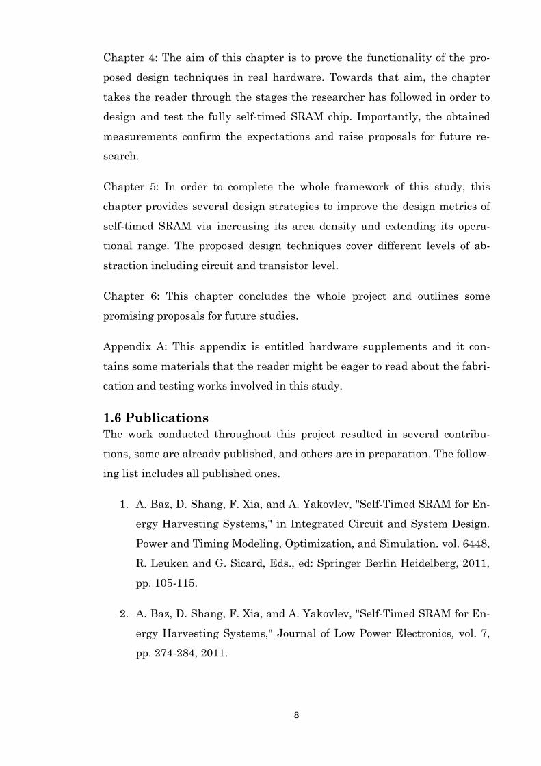
the conductor changes [1]. For instance, if an inductor coil is attached to any
vibration source and permanent magnets are used to produce magnetic field
through the coil (as shown in the figure below [1]). Then the relative dis-
placement caused by the vibrations will change the magnetic flux through
the coil and hence generate electric current inside it.
Figure 2.1 Electromagnetic transduction technique.
In this transduction mechanism, the voltage across the coil is proportional
to the strength of the magnetic field, the velocity of vibration, and the num-
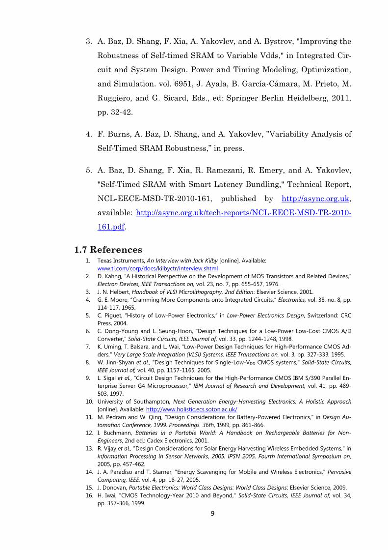
ber of turns of the coil [1, 3-5]. Piezoelectric harvesters employ the piezoelec-
tric effect that exists in some materials like crystals and certain ceramics.
Piezoelectric effect is the ability of generating an electrical potential in re-
sponse to applied mechanical stress [3-5] as shown in the figure below [1].
Figure 2.2 Piezoelectric transduction technique.
14
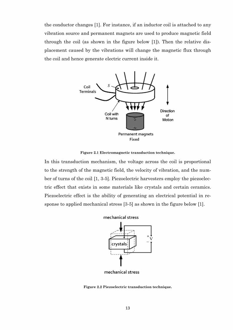
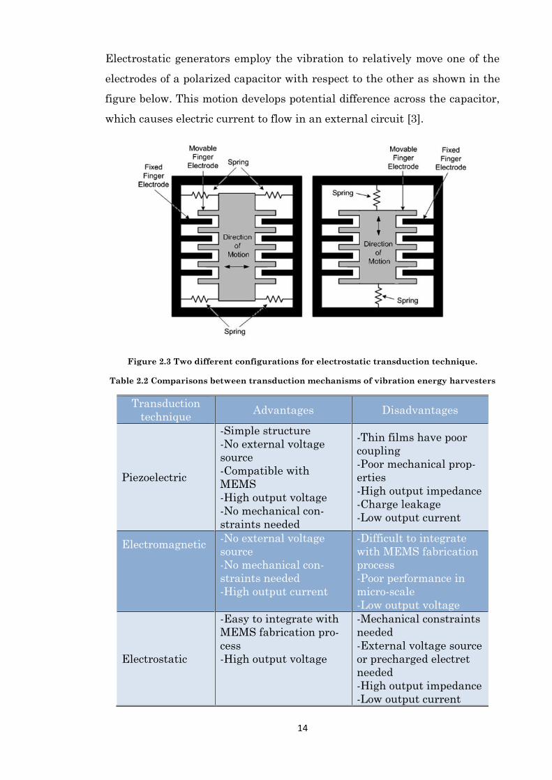
Electrostatic generators employ the vibration to relatively move one of the
electrodes of a polarized capacitor with respect to the other as shown in the
figure below. This motion develops potential difference across the capacitor,
which causes electric current to flow in an external circuit [3].
Figure 2.3 Two different configurations for electrostatic transduction technique.
Table 2.2 Comparisons between transduction mechanisms of vibration energy harvesters
Transduction
technique Advantages Disadvantages
Piezoelectric
-Simple structure
-No external voltage
source
-Compatible with
MEMS
-High output voltage
-No mechanical con-
straints needed
-Thin films have poor
coupling
-Poor mechanical prop-
erties
-High output impedance
-Charge leakage
-Low output current
Electromagnetic
-No external voltage
source
-No mechanical con-
straints needed
-High output current
-Difficult to integrate
with MEMS fabrication
process
-Poor performance in
micro-scale
-Low output voltage
Electrostatic
-Easy to integrate with
MEMS fabrication pro-
cess
-High output voltage
-Mechanical constraints
needed
-External voltage source
or precharged electret
needed
-High output impedance
-Low output current
15
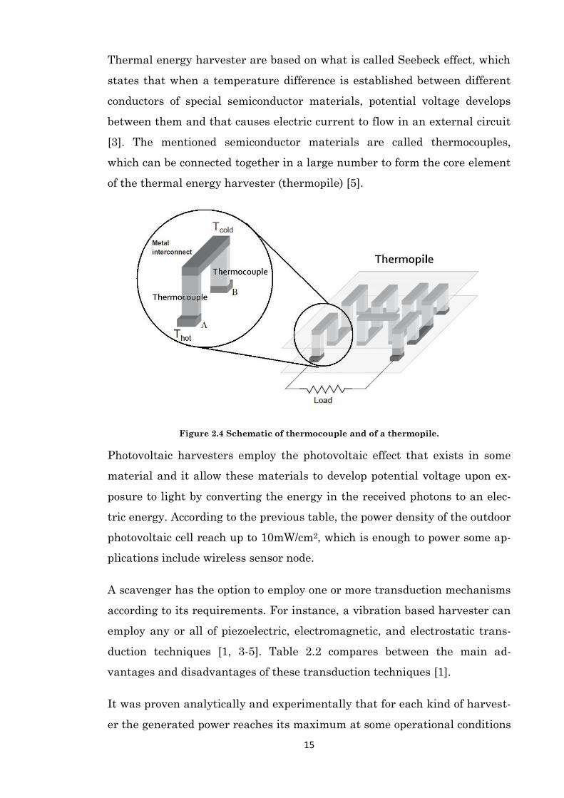
Thermal energy harvester are based on what is called Seebeck effect, which
states that when a temperature difference is established between different
conductors of special semiconductor materials, potential voltage develops
between them and that causes electric current to flow in an external circuit
[3]. The mentioned semiconductor materials are called thermocouples,
which can be connected together in a large number to form the core element
of the thermal energy harvester (thermopile) [5].
Figure 2.4 Schematic of thermocouple and of a thermopile.
Photovoltaic harvesters employ the photovoltaic effect that exists in some
material and it allow these materials to develop potential voltage upon ex-
posure to light by converting the energy in the received photons to an elec-
tric energy. According to the previous table, the power density of the outdoor
photovoltaic cell reach up to 10mW/cm2, which is enough to power some ap-
plications include wireless sensor node.
A scavenger has the option to employ one or more transduction mechanisms
according to its requirements. For instance, a vibration based harvester can
employ any or all of piezoelectric, electromagnetic, and electrostatic trans-
duction techniques [1, 3-5]. Table 2.2 compares between the main ad-
vantages and disadvantages of these transduction techniques [1].
It was proven analytically and experimentally that for each kind of harvest-
er the generated power reaches its maximum at some operational conditions
16
and it drops otherwise [3]. Vibration based power generator is a resonant
system, therefore, it produces maximum power when its resonant frequency
matches the kinetic vibration frequency [3]. In the case of harvesting energy
from temperature difference, the maximum power is generated when the
thermal resistance of the thermocouples equates to that of the air gap [3, 6].
Photovoltaic maximum power depends upon light intensity and temperature
[7]. Accordingly, adaptive techniques are required, in the micro-generator,
in order to boost its efficiency and decrease the loss resulting from environ-
mental and operational conditions [1, 3].
Extracting maximum power from a scavenger, that can be delivered to the
load is another issue called Maximum Power Point Tracking (MPPT). This
design technique requires considering the internal impedance of the har-
vester, which significantly varies based upon the type of the harvester,
ranging from a few ohms for the thermal harvester to tens of kilohms for vi-
bration ones [4].
In the case that two or more sources of energy are available in the environ-
ment surrounding the electronic system, a technique called Multi-Modal en-
ergy harvesting can be employed to improve the amount of supplied energy.
A prototype is reported in [8] that combines electromagnetic and piezoelec-
tric energy harvesters, where the power generated from the fabricated de-
vice was found to be 0.25W and 0.25mW using the electromagnetic and pie-
zoelectric mechanism respectively.
The most important performance metrics of the harvester that the applica-
tion needs to consider are the range of output voltages and power density,
which is the amount of generated power per unit volume. These two proper-
ties are significantly dominated by the material used to implement the de-
vice, the transduction scheme, the type of the ambient energy, and the
source of it (e.g. human or industrial [5]). Output voltage ranges from hun-
dreds mV, in the case of photovoltaic cells, to a few volts, in the case of vi-
bration harvester [4]. Power density is in the range of a few to a few hun-
dreds of µW/cm3 and might reach up to tens of mW/cm3 in the case of out-
door solar harvesters.

17
2.2.2 Energy Harvesting Electronics
The portable electronics era put hard pressure on several performance met-
rics of the electronic systems, power consumption is at the top of them. Con-
sequently, several energy and power minimization techniques were intro-
duced to the area, which resulted in operating fully functional SoC with very
low energy consumption. Examples include an 8-bit sub-threshold processor
that is fully functional from as low as 200mV and consumes
3.5pJ/instruction at 350mV [9], and a 16-bit microcontroller that consumes
27.2pJ/cycle at its minimum energy voltage [10]. In the case of power re-
stricted applications, the processor can adaptively operate down to 160mV
and draws 11nW at 710Hz [9] while the microcontroller consumes around
12µW [10].
Comparing the range of power consumption of those carefully designed mi-
croelectronic systems with the range of power generated from optimized
harvesters, as mentioned earlier, results in the fact that both are in the
same order of magnitude. This has created a clear opportunity to develop a
new generation of microelectronics systems that can be self-powered. To-
wards this goal, many projects were funded and hundreds of research pa-
pers were published around the world [11, 12]. All these studies were con-
ducted because numerous challenges in this era have not yet been ad-
dressed.
For instance, energy harvesting systems rely upon random amounts of en-
ergy and nondeterministic voltage levels, which can be interrupted at any
time. Therefore, they require new design strategies that are more adaptive,
clever, and energy-aware. Such a design technique might provide the system
with the highest performance whenever energy is available and at the same
time provide a fallback strategy when the available energy drops to a cer-
tain level. This strategy must have the highest priority of saving the im-
portant data as well as completing the requested tasks within the supplied
amount of energy even if the performance is sacrificed. This design tech-
nique should be energy aware in the sense that all the time it does not
spend more than the harvested amount of energy. Moreover, the overall cir-
18
cuitry has to consider other challenges involved in the technology node such
as high off-currents and process variations if exist.
Starting from this vision, the researcher begins his study towards proposing
new design techniques for these systems powered by harvesters in order to
enable the era of self-powered electronics.
2.3 SRAM
Static Random Access Memory (SRAM) is a fundamental and vital subsys-
tem for all computational systems. This type of memory is volatile as it does
lose its contents when the power supply is lost and it is called static because
the stored data do not require refreshing as in the case of DRAM. The term
random access means that any memory word can be accessed arbitrary and
not necessarily sequentially. SRAM is a subsystem because it is employed as
a crucial part of computational systems to store instructions, operands, and
results. In personal computers, SRAM is used as on-chip Level 1 (L1) and
Level 2 (L2) caches to exchange data between main memory and CPU regis-
ters [13].
2.3.1 SRAM Structure and Operational States
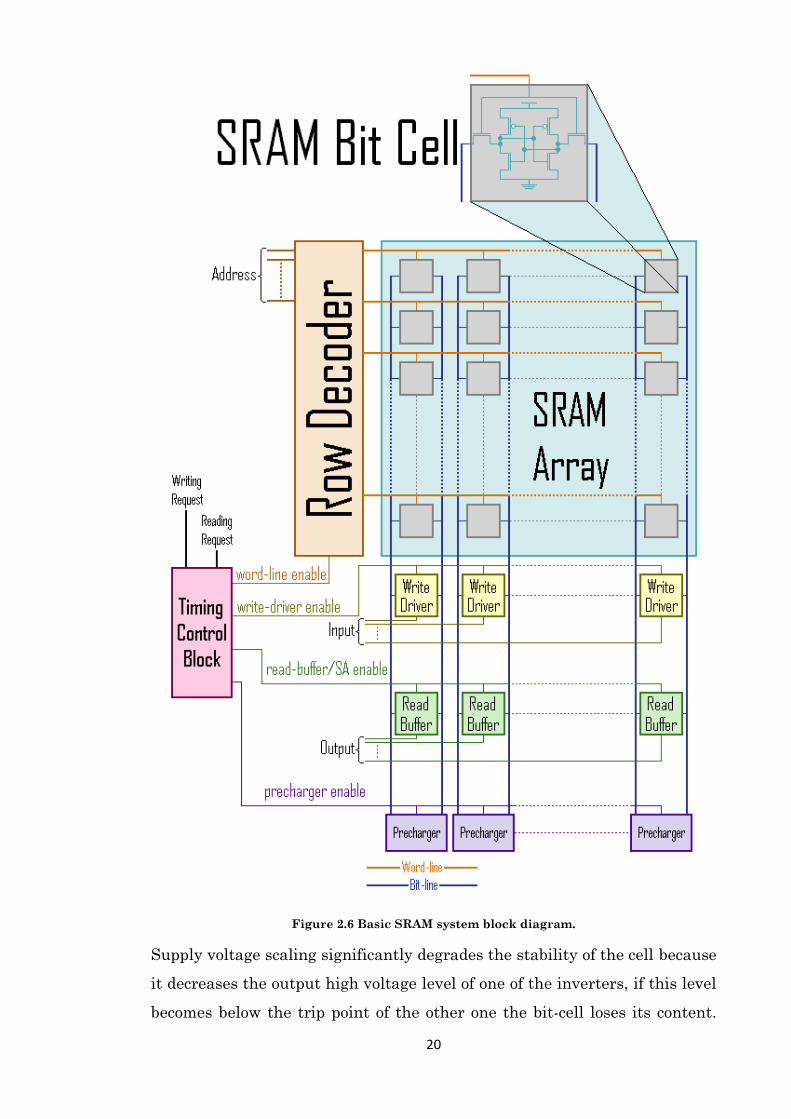
Figure 2.6 shows the block diagram of a basic SRAM system, its workhorse
is the bit-cell, which is a component able to store only one bit of data, either
0 or 1. This cell is repeated tens of thousands of times and organized in rows
and columns to form a sub array. Each bank is surrounded by several auxil-
iary circuits, which include decoder, prechargers, write drivers, read buffers,
column multiplexers, and sense amplifiers, to complete the functionality of
the memory. All cells in the same column share a common connection from
sides called a pair of bit-lines and all cells in the same row share a common
link called a word-line. A pair of bit-lines is used by the write drivers to
write the data into the cells during writing operation as well as is used by
the read buffers to read the data from the cells during reading process.
Word-line is activated by the decoder to allow the bit-lines accessing the
cross coupled inverters via the access transistors. Several bit-lines might
share the same auxiliary circuits using a column multiplexer so as to im-
19
prove the area density of the SRAM. The size of the SRAM can be increased
by including many banks in the same SRAM system.
All signals in the SRAM system are monitored and controlled by a vital
component called timing control block, which synchronizes all signals in the
memory in order to guarantee safe and successful operation during each op-
erational state of the memory as will be described in the following.
2.3.1.1 Holding State
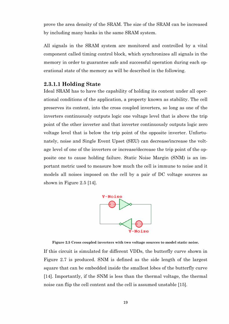
Ideal SRAM has to have the capability of holding its content under all oper-
ational conditions of the application, a property known as stability. The cell
preserves its content, into the cross coupled inverters, so long as one of the
inverters continuously outputs logic one voltage level that is above the trip
point of the other inverter and that inverter continuously outputs logic zero
voltage level that is below the trip point of the opposite inverter. Unfortu-
nately, noise and Single Event Upset (SEU) can decrease/increase the volt-
age level of one of the inverters or increase/decrease the trip point of the op-
posite one to cause holding failure. Static Noise Margin (SNM) is an im-
portant metric used to measure how much the cell is immune to noise and it
models all noises imposed on the cell by a pair of DC voltage sources as
shown in Figure 2.5 [14].
Figure 2.5 Cross coupled inverters with two voltage sources to model static noise.
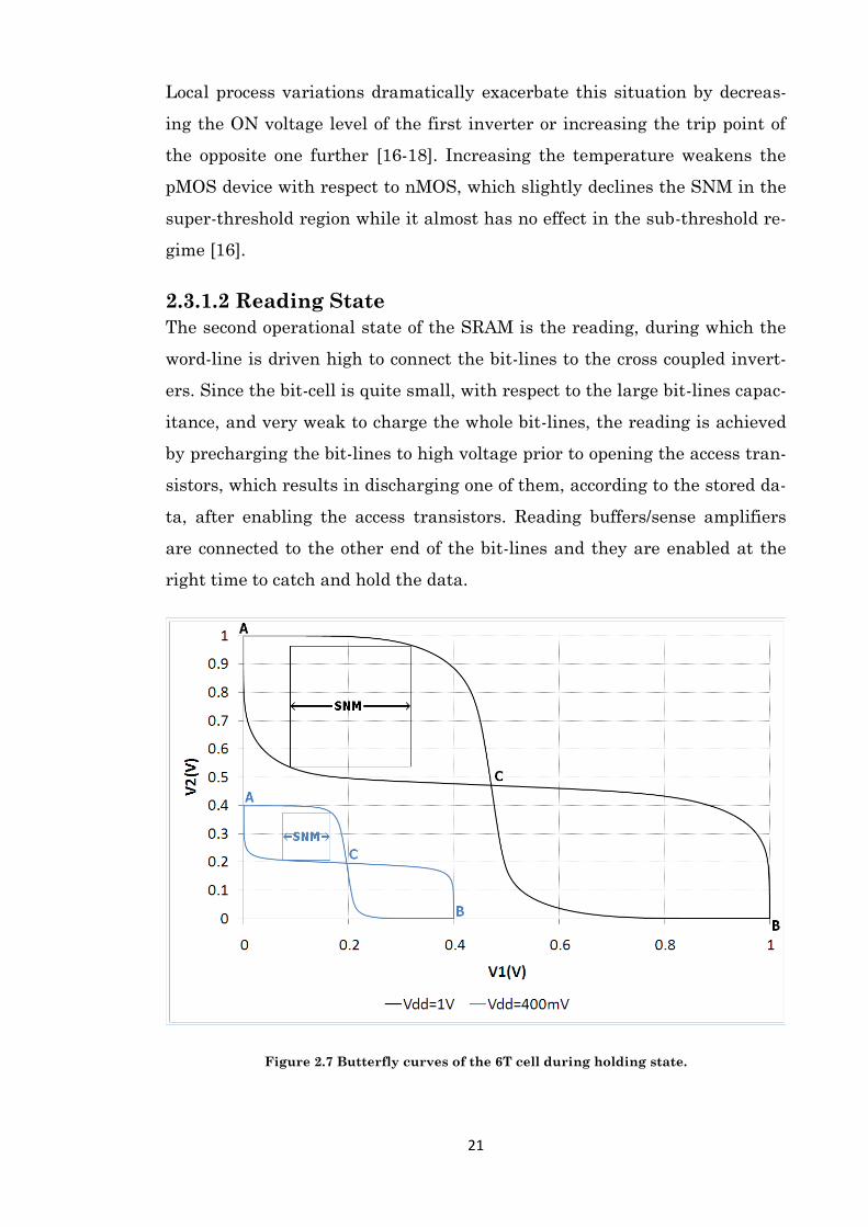
If this circuit is simulated for different VDDs, the butterfly curve shown in
Figure 2.7 is produced. SNM is defined as the side length of the largest
square that can be embedded inside the smallest lobes of the butterfly curve
[14]. Importantly, if the SNM is less than the thermal voltage, the thermal
noise can flip the cell content and the cell is assumed unstable [15].
20
Figure 2.6 Basic SRAM system block diagram.
Supply voltage scaling significantly degrades the stability of the cell because
it decreases the output high voltage level of one of the inverters, if this level
becomes below the trip point of the other one the bit-cell loses its content.
21
Local process variations dramatically exacerbate this situation by decreas-
ing the ON voltage level of the first inverter or increasing the trip point of
the opposite one further [16-18]. Increasing the temperature weakens the
pMOS device with respect to nMOS, which slightly declines the SNM in the
super-threshold region while it almost has no effect in the sub-threshold re-
gime [16].
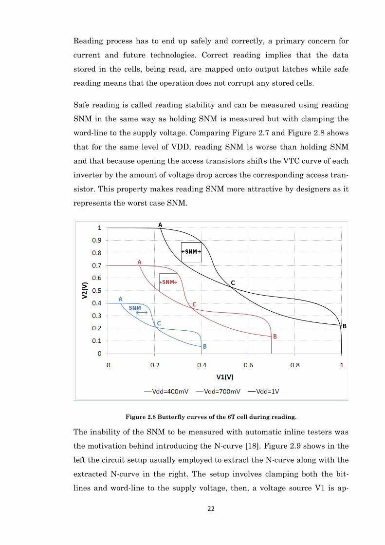
2.3.1.2 Reading State
The second operational state of the SRAM is the reading, during which the
word-line is driven high to connect the bit-lines to the cross coupled invert-
ers. Since the bit-cell is quite small, with respect to the large bit-lines capac-
itance, and very weak to charge the whole bit-lines, the reading is achieved
by precharging the bit-lines to high voltage prior to opening the access tran-
sistors, which results in discharging one of them, according to the stored da-
ta, after enabling the access transistors. Reading buffers/sense amplifiers
are connected to the other end of the bit-lines and they are enabled at the
right time to catch and hold the data.
Figure 2.7 Butterfly curves of the 6T cell during holding state.
22
Reading process has to end up safely and correctly, a primary concern for
current and future technologies. Correct reading implies that the data
stored in the cells, being read, are mapped onto output latches while safe
reading means that the operation does not corrupt any stored cells.
Safe reading is called reading stability and can be measured using reading
SNM in the same way as holding SNM is measured but with clamping the
word-line to the supply voltage. Comparing Figure 2.7 and Figure 2.8 shows
that for the same level of VDD, reading SNM is worse than holding SNM
and that because opening the access transistors shifts the VTC curve of each
inverter by the amount of voltage drop across the corresponding access tran-
sistor. This property makes reading SNM more attractive by designers as it
represents the worst case SNM.
Figure 2.8 Butterfly curves of the 6T cell during reading.
The inability of the SNM to be measured with automatic inline testers was
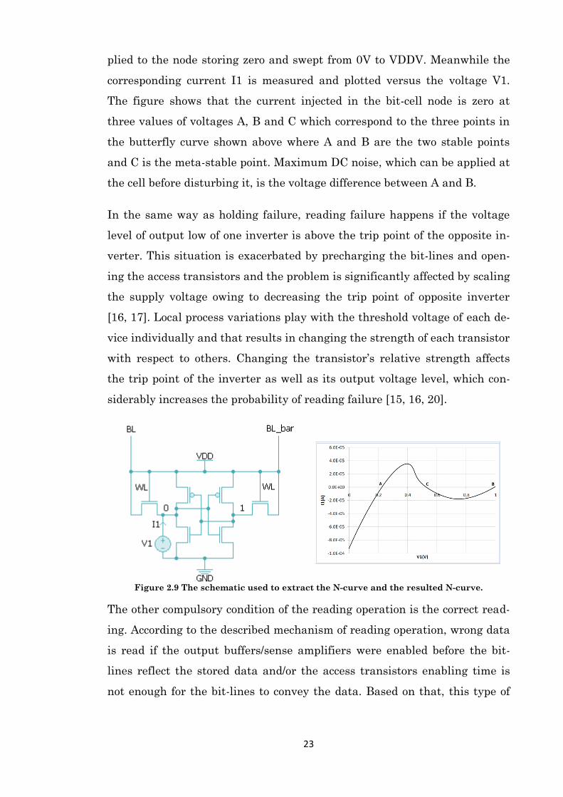
the motivation behind introducing the N-curve [18]. Figure 2.9 shows in the
left the circuit setup usually employed to extract the N-curve along with the
extracted N-curve in the right. The setup involves clamping both the bit-
lines and word-line to the supply voltage, then, a voltage source V1 is ap-
23
plied to the node storing zero and swept from 0V to VDDV. Meanwhile the
corresponding current I1 is measured and plotted versus the voltage V1.
The figure shows that the current injected in the bit-cell node is zero at
three values of voltages A, B and C which correspond to the three points in
the butterfly curve shown above where A and B are the two stable points
and C is the meta-stable point. Maximum DC noise, which can be applied at
the cell before disturbing it, is the voltage difference between A and B.
In the same way as holding failure, reading failure happens if the voltage
level of output low of one inverter is above the trip point of the opposite in-
verter. This situation is exacerbated by precharging the bit-lines and open-
ing the access transistors and the problem is significantly affected by scaling
the supply voltage owing to decreasing the trip point of opposite inverter
[16, 17]. Local process variations play with the threshold voltage of each de-
vice individually and that results in changing the strength of each transistor
with respect to others. Changing the transistor’s relative strength affects
the trip point of the inverter as well as its output voltage level, which con-
siderably increases the probability of reading failure [15, 16, 20].
Figure 2.9 The schematic used to extract the N-curve and the resulted N-curve.
The other compulsory condition of the reading operation is the correct read-
ing. According to the described mechanism of reading operation, wrong data
is read if the output buffers/sense amplifiers were enabled before the bit-
lines reflect the stored data and/or the access transistors enabling time is
not enough for the bit-lines to convey the data. Based on that, this type of
24
failure manifests itself as a timing issue, hence, it is also known as access
time failure [15, 17].
Again, supply voltage scaling and local process variations change the char-
acteristic of individual device differently and that results in considerable
variations in reading timing, which was calibrated during the design time,
to end up with access time failure in the real silicon.
2.3.1.3 Writing State
The last operational state of the SRAM is the writing operation, during
which the system has to have the ability to successfully write new data to
the bit-cells. The new data might be the same as or opposite of the stored
ones, nevertheless, opposite data is always assumed as it involves more ac-
tions (e.g. flipping the cells) and hence it represents the worst case writing.
Based on that successful writing involves discharging the node holding high
voltage, through its corresponding bit-line, below the opposite inverter trip
point within the time when access transistors are enabled. Write driver is
the component in charge of driving the bit-line to discharge that node,
where the final voltage of the high voltage node is determined by the voltage
divider between the corresponding pull-up transistor and access transistor.
Moreover, since the access transistors are enabled for a limited time only,
the final voltage is also affected by the discharging current, that is the dif-
ference in ON current between the pull-up and access transistor [17].
Successful writing as described above is a feature called write-ability, which
can be measured by the writing SNM as shown in the right of Figure 2.10,
where the circuit setup appears in the left. If the side of the largest square
that can be embedded between the two curves is larger than zero, the cell is
then writeable. Similar to the case of reading, the same N-curve can be used
to measure the write-ability, which equals to the voltage difference between
point C and B in Figure 2.9.

25
Figure 2.10 The schematic used to extract the WSNM together with the extracted curves.
Increasing the temperature and/or decreasing the VDD decrease the ON-
current of the transistors [21] and that significantly degrades the write-
ability of the bit-cell [17, 18]. Local process variations have severe negative
effects on write-ability owing to its ability to change the strength and ON
current of each transistor in the cell individually [17, 18].
2.3.2 SRAM Design Challenges
SRAM design margin shrinks as the technology scales down and that in-
creases the challenges associated with it, especially for current and future
processes. Table 2.3 shows how the scaling of transistor size affects various
parameters of the device [19].
Table 2.3 Scaling parameters.
Parameter Scaling factor
Gate length 1/s
Oxide thickness 1/s
Junction depth 1/s
Drain voltage 1/s
Drain current 1/s
Threshold voltage 1/s
Gate area 1/s2
Supply voltage 1/s
Number of transistors s2
The elusive aim of all memory designers is to propose a single design that is
optimized in terms of performance, density, power dissipation/energy con-
sumptions, robustness, manufacturing yield, testability, scalability, and
modularity. Unfortunately, such an SRAM has not yet been developed nor
expected to appear in the future [22]. Accordingly, this section is dedicated
to discuss the most common challenges in SRAM design, which are listed in
26
the following paragraphs followed by a section containing possible solutions
if any exists.
The first challenge results from the fundamental conflict in the design re-
quirements of the 6T bit-cell. According to the aforementioned discussion,
write-ability requires decreasing the relative strength of the pull-up transis-
tors to access transistors (pull-up ratio) and increasing the relative strength
of the pull-up transistors to pull-down transistors. For the same cell, read-
stability requires increasing the relative strength of the pull-down transis-
tors to access transistors (cell ratio) [17, 18].
High density SoCs require a bit-cell designed upon minimum or near mini-
mal feature size devices [23-25]. Nevertheless, the standard deviation of the
device threshold voltage variations is inversely proportional to the square
root of the effective device area (Pelgrom's law) [26, 27]. Accordingly, the
smaller the cell area is the higher variations it experiences and the less ro-
bustness it has [24].
With more than 90% of the chip area occupied by the memory [28] and as
much as 40% of the total power in 90nm generation wasted in leakage
[29, 30], leakage power became one of the crucial SRAM design challenges
in submicron process technologies, especially during the standby mode. Fig-
ure 2.11 depicts the current leakage from the 6T bit-cell, during holding
state. Moreover, systematic and/or random parameter variations, especially
those affecting threshold voltage, considerably play with the leakage energy
from two aspects. On the one hand, as the variations decrease the threshold
voltage of the device, it leaks more current. On the other hand, as the
threshold voltage decreases, the device becomes faster and its operation
time decreases which reflected back upon its energy.
27
Figure 2.11 Leakage currents in the 6T cell.
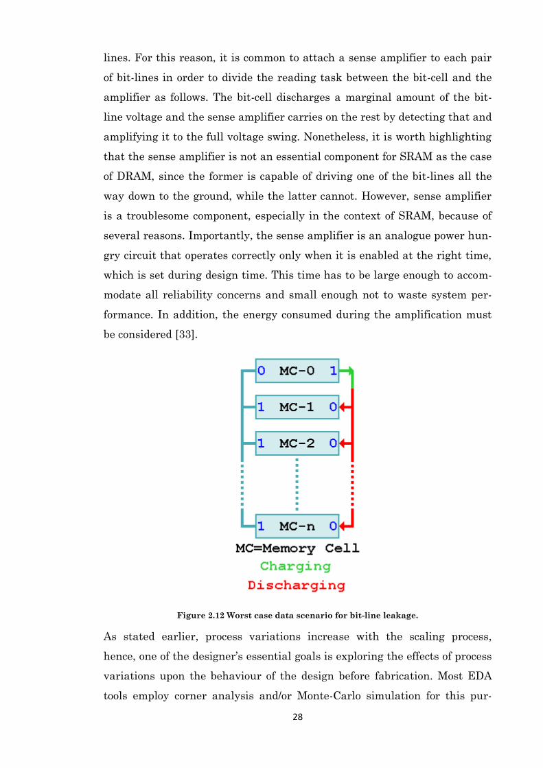
In addition to wasting energy, leakage can corrupt data during SRAM oper-
ations. This occurs because bit-lines are the only way the peripheral circuits
communicate with bit-cells, however, while the signals carried by the bit-
lines have to be controlled by the accessed cells only, the leakage current
from un-accessed cells strongly affect them. One of the scenarios represent-
ing this issue might be a pair of bit-lines, one of them is correctly pulled-
down by the stored data of the accessed cell while the other one is errone-
ously pulled-down by the leakage from un-accessed cells. The problem dete-
riorates as the number of cells per bit-lines increases [31], temperature in-
creases and/or process variations decrease the threshold voltage of the de-
vices [32]. The worst case data scenario is shown in Figure 2.12 and it oc-
curs when accessing one of the bit-cells that stores data complement to the
data stored in all other cells in the same pair of bit-lines. This case involves
fighting between the accessed cell and all un-accessed cells, while the former
tries to keep the charge in the bit-lines the latter discharges it.
The performance of a SoC is dominated by that of its corresponding memory,
as the latter is involved in all stages of computations. Accordingly, it is the
aim of the designers to cut down the operation time, especially the reading
operation as it consists of discharging the large capacitance of one of the bit-
28
lines. For this reason, it is common to attach a sense amplifier to each pair
of bit-lines in order to divide the reading task between the bit-cell and the
amplifier as follows. The bit-cell discharges a marginal amount of the bit-
line voltage and the sense amplifier carries on the rest by detecting that and
amplifying it to the full voltage swing. Nonetheless, it is worth highlighting
that the sense amplifier is not an essential component for SRAM as the case
of DRAM, since the former is capable of driving one of the bit-lines all the
way down to the ground, while the latter cannot. However, sense amplifier
is a troublesome component, especially in the context of SRAM, because of
several reasons. Importantly, the sense amplifier is an analogue power hun-
gry circuit that operates correctly only when it is enabled at the right time,
which is set during design time. This time has to be large enough to accom-
modate all reliability concerns and small enough not to waste system per-
formance. In addition, the energy consumed during the amplification must
be considered [33].
Figure 2.12 Worst case data scenario for bit-line leakage.
As stated earlier, process variations increase with the scaling process,
hence, one of the designer’s essential goals is exploring the effects of process
variations upon the behaviour of the design before fabrication. Most EDA
tools employ corner analysis and/or Monte-Carlo simulation for this pur-
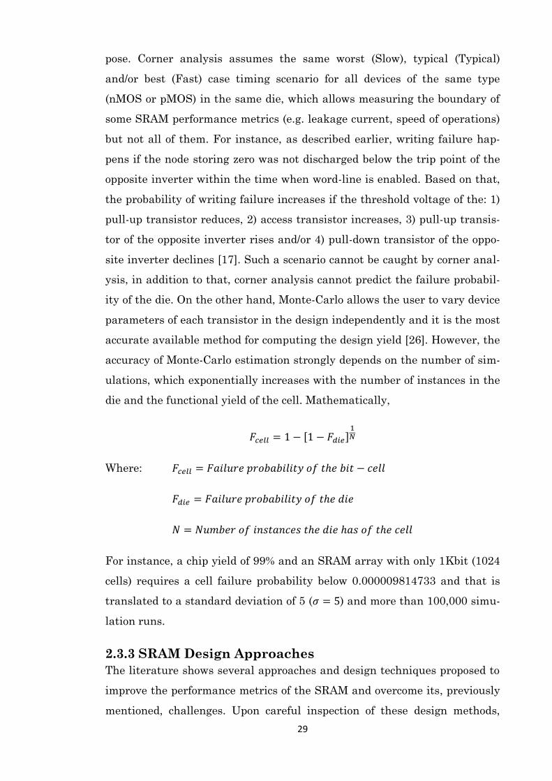
29
pose. Corner analysis assumes the same worst (Slow), typical (Typical)
and/or best (Fast) case timing scenario for all devices of the same type
(nMOS or pMOS) in the same die, which allows measuring the boundary of
some SRAM performance metrics (e.g. leakage current, speed of operations)
but not all of them. For instance, as described earlier, writing failure hap-
pens if the node storing zero was not discharged below the trip point of the
opposite inverter within the time when word-line is enabled. Based on that,
the probability of writing failure increases if the threshold voltage of the: 1)
pull-up transistor reduces, 2) access transistor increases, 3) pull-up transis-
tor of the opposite inverter rises and/or 4) pull-down transistor of the oppo-
site inverter declines [17]. Such a scenario cannot be caught by corner anal-
ysis, in addition to that, corner analysis cannot predict the failure probabil-
ity of the die. On the other hand, Monte-Carlo allows the user to vary device
parameters of each transistor in the design independently and it is the most
accurate available method for computing the design yield [26]. However, the
accuracy of Monte-Carlo estimation strongly depends on the number of sim-
ulations, which exponentially increases with the number of instances in the
die and the functional yield of the cell. Mathematically,
[ ]
Where:
For instance, a chip yield of 99% and an SRAM array with only 1Kbit (1024
cells) requires a cell failure probability below 0.000009814733 and that is
translated to a standard deviation of 5 ( ) and more than 100,000 simu-
lation runs.
2.3.3 SRAM Design Approaches
The literature shows several approaches and design techniques proposed to
improve the performance metrics of the SRAM and overcome its, previously
mentioned, challenges. Upon careful inspection of these design methods,
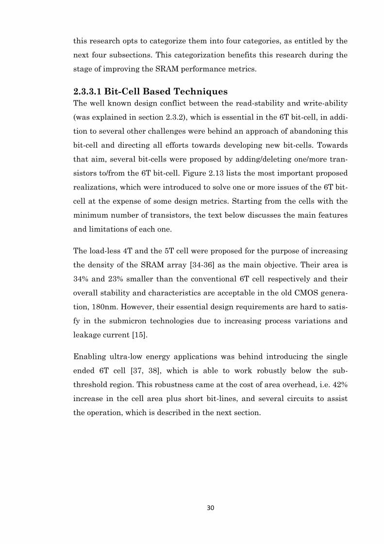
30
this research opts to categorize them into four categories, as entitled by the
next four subsections. This categorization benefits this research during the
stage of improving the SRAM performance metrics.
2.3.3.1 Bit-Cell Based Techniques
The well known design conflict between the read-stability and write-ability
(was explained in section 2.3.2), which is essential in the 6T bit-cell, in addi-
tion to several other challenges were behind an approach of abandoning this
bit-cell and directing all efforts towards developing new bit-cells. Towards
that aim, several bit-cells were proposed by adding/deleting one/more tran-
sistors to/from the 6T bit-cell. Figure 2.13 lists the most important proposed
realizations, which were introduced to solve one or more issues of the 6T bit-
cell at the expense of some design metrics. Starting from the cells with the
minimum number of transistors, the text below discusses the main features
and limitations of each one.
The load-less 4T and the 5T cell were proposed for the purpose of increasing
the density of the SRAM array [34-36] as the main objective. Their area is
34% and 23% smaller than the conventional 6T cell respectively and their
overall stability and characteristics are acceptable in the old CMOS genera-
tion, 180nm. However, their essential design requirements are hard to satis-
fy in the submicron technologies due to increasing process variations and
leakage current [15].
Enabling ultra-low energy applications was behind introducing the single
ended 6T cell [37, 38], which is able to work robustly below the sub-
threshold region. This robustness came at the cost of area overhead, i.e. 42%
increase in the cell area plus short bit-lines, and several circuits to assist
the operation, which is described in the next section.
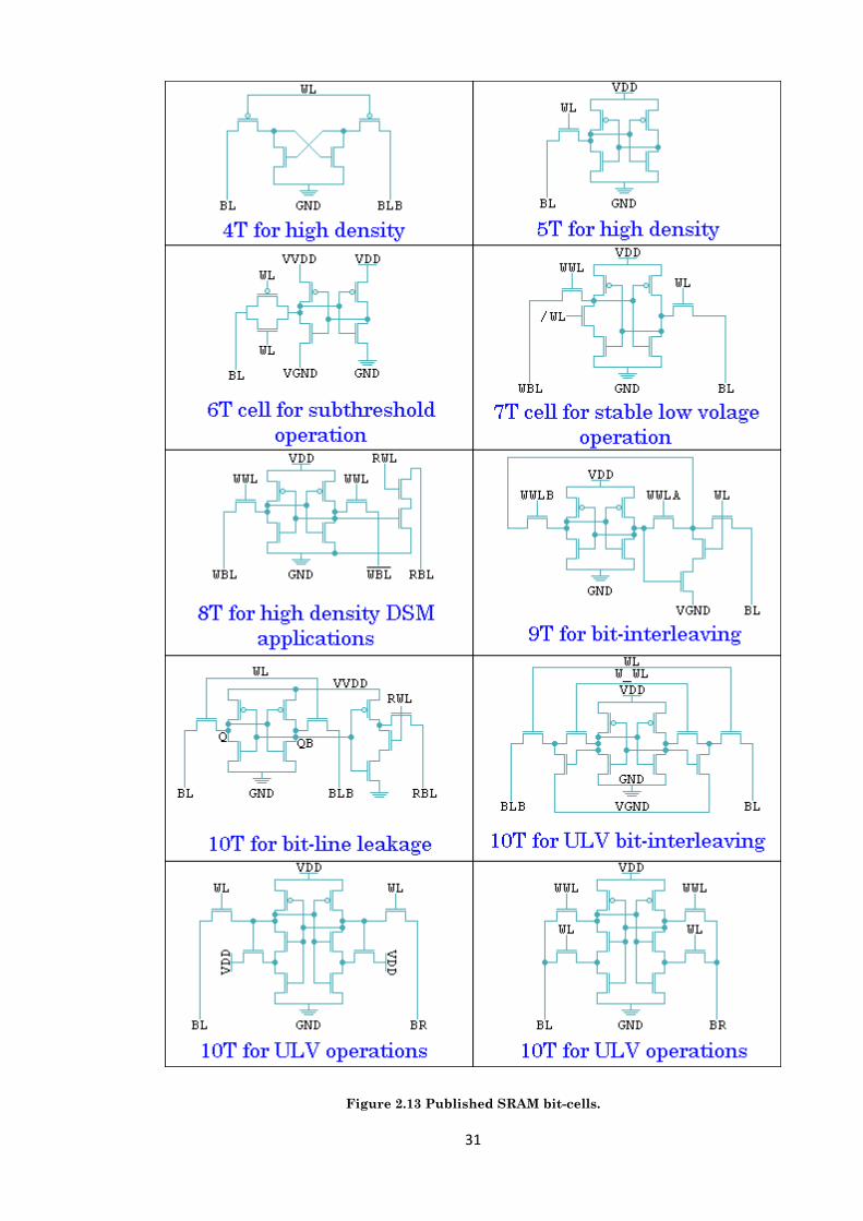
31
Figure 2.13 Published SRAM bit-cells.
32
The authors of [39] exploited the intuitive observation that SRAM operation
time is determined by the slowest cell and that is usually the furthest cell
from peripheral circuitry in the block due to the interconnect delay. Accord-
ingly, it is proposed to slow down all other bit-cells which are faster than the
slowest cell by replacing some/all of their normal transistors with high
transistors in order to decrease the leakage. The replacing is accom-
plished via an algorithm to guarantee that the swapping process will not re-
sult in reliability degradation while optimizing the leakage reduction. The
method was extended later in [40] to cover dual along with dual , both
of which showed a leakage reduction ranging from 30%-40% for small size
SRAM bank. The drawbacks of this technique include changing the design
flow to include hybrid cells and decreasing the manufacturing yield due to
adding mask layer for the high and .
The single ended asymmetrical 7T cell with triple word-lines allowed reduc-
ing the active power via decreasing the VDD while maintaining the reading
stability. To enable an active operation fairly above the threshold voltage,
the cell incurs 13% area overhead per cell and its layout forms an L-shape,
which results in a useless gap, enough to accommodate two transistors, for
each two abutted cells [41, 42].
The single ended 8T cell [23] aims to resolve the fundamental design conflict
in the 6T cell via adding two more transistors dedicated for reading to pre-
vent it from upsetting the stored data. This isolation gives the opportunity
to optimize the cross-coupled inverter along with the access transistors for
write-ability and hold-stability. This bit-cell has demonstrated its full func-
tionality for a medium size memory system, 256kb, implemented using
submicron technology, 65nm, down to the sub-threshold region [31]. Howev-
er, the cell is 30% bigger than the conventional cell and its single ended
sensing decreases the area efficiency from 70% to 50% [15, 23].
A triple word-lines and a bit-line single ended 9T cell was proposed in [43],
which incurs 97% area overhead and requires several operational assist
techniques to enable safe sub-threshold operation.
33
Published papers and their citations indicate that ten transistors are almost
the maximum acceptable number of transistors per cell, accordingly several
10T bit-cells were proposed as described in the following paragraphs.
The motivation for the proposed 10T cell in [44] was to minimize the energy
per operation via working in the sub-threshold regime and cut down the bit-
line leakage, which saves more power and allows increasing bit-line size.
The main constraints of this design are 66% area overhead, and the need of
adding assisting technique in order to make the cell writeable.
Another differential dual word-line 10T cell was proposed in [45] to provide
efficient bit-interleaving scheme for the purpose of mitigating soft errors
and enhancing ultra-low voltage operations. Real silicon proved that this
design is able to work down to 180mV for 32kb array implemented in 90nm
technology, a remarkable feat. Nonetheless, the cell suffers from an area
penalty of 61% comparable to the single ended 8T cell and the essential need
of 30% boosted supply voltage for writing operation, which significantly de-
teriorates the area.
The last two cells described here abandoned the cross-coupled inverters and
replaced them with cross-coupled Schmitt Trigger (ST) based inverters [46-
48], they are called ST-1 and ST-2. These two designs were proposed in light
of the fact that Schmitt trigger employs a built-in feedback mechanism to
mitigate process variations and improve the noise margin of the cell. ST-1
and ST-2 incurs more than 100% area overhead. Nevertheless, they are skil-
ful at enabling ultra-low voltage/power applications via operating the
memory system in the deep sub-threshold regime while save safe operations
[15].
Meaningful comparison between these cells cannot be concluded because
each one was proposed for different application and was tested in different
technology node. Finally, it is worth highlighting that in all of the previously
proposed cells, improving the robustness of the cell allows decreasing the
supply voltage during reading, writing, or holding state, which is reflected
upon the active and leakage power dissipation of the whole memory system.
34
Accordingly, improving the robustness of SRAM cuts down its energy con-
sumption.
2.3.3.2 Voltage Level Based Techniques
The second category of approaches, for improving SRAM performance pa-
rameters, involves designing auxiliary circuits to play with the voltage level
of one or more signals in the SRAM system. Designers have the choice of
whether to combine this technique with the previous one, new bit-cell
[31, 44, 49, 50], or serve it separately based on the 6T cell [51-57]. Im-
portantly, this technique requires redesigning the timing control circuitry in
order to adjust the timing of the manipulated signals. Nevertheless, the
challenge here is to guarantee the correct operation of the added timing cir-
cuits across the complete operational range of the application [31, 44, 49-
55, 57]. The following text in this section discusses the most important volt-
age level design techniques employed in the SRAM, each in a separate par-
agraph. The text starts by explaining the theory behind each design method,
followed by some noticeable examples from the literature, and ended by the
main limitations of that method.
As described earlier, successful writing must involve decreasing the voltage
of the node storing one below the trip point of the opposite inverter during
the time when word-line signal is high. Based on that, write-ability im-
proves as that voltage node decreases or trip point increases during the
specified time. The voltage divider between access transistor and pull-up
transistors determines the minimum voltage at the node storing one, hence
increasing the relative strength of the access transistor to pull-up transis-
tors, i.e. pull-up ratio, enhances the write-ability. Based on that, the adap-
tive increasing of the differential voltage between word-line and VDD de-
creases write failure. At the same time, trip point of the opposite inverter
increases as its ground voltage rises, accordingly raising the cell ground
voltage enhances the write-ability as well. Recent works proposed several
circuit realizations to implement the described assisting technique different-
ly. In [44, 49] cell VDD is floated using a gated transistor while the word-
line signal is kept at its nominal value to improve the pull-up ratio. In con-
35
trast, it was proposed in [49, 51-53] to decrease the cell VDD instead of just
floating it as the write-ability of the relevant cell is a challenging problem.
All these write-ability enhancement circuit techniques incur performance
degradation and area overhead per bit-cell for switching and routing the
other supply voltage respectively. In addition to that, they require an accu-
rate timing circuit for swapping the VDDs as it is compulsory to raise the
cell supplied voltage to an acceptable level before closing the access transis-
tors in order to allow new data settle inside the cell. The area overhead of
the assist technique in 10T cell is less than that in 6T, since the latter re-
quire two global power supplies supplied externally, however, the former
suffer from the process variations of the gated transistor. In [57], the other
cell voltage is globally generated via an on-chip regulator, which requires a
reference voltage and has an amplifier.
Similarly, a sufficient level of stability during reading requires that the pre-
charged bit-line does not raise the voltage of the node storing zero above the
trip point of the opposite inverter during the time when the access transis-
tors are enabled. Based on that, stability improves as that voltage node de-
creases or the trip point increases during the specified time. The bit-line
precharged voltage divided between the access transistor and pull-down
transistor determines the maximum voltage at the node storing zero. Hence,
increasing the relative strength of the access transistor to the pull-down
transistor, i.e. cell ratio, or decreasing the precharged voltage of the bit-lines
enhances the reading stability. At the same time, the trip point of the oppo-
site inverter increases as supplied voltage rises, accordingly, raising the cell
supplied voltage enhances the stability of the cell. Again, several circuit re-
alizations are implemented to adaptively control the cell ratio, differently. It
was proposed in [51, 52] to connect the read cell to a higher voltage supplied
externally while in [53] a dynamic analogue circuit was implemented for
playing with the level of word-line signal. The authors of [58] found that for
maximum read margin, is the optimum voltage value for pre-
charging the bit-lines. As before, the main limitations of these designs in-
clude area and performance overhead.
36
Virtual ground is able to limit the off current of un-accessed cells, however,
it involves a design conflict since the virtual ground should be able to block
as much leakage current as possible from un-accessed rows while sink as
much current as possible from the accessed row. This concern can be
addressed by controlling the virtual ground inverter with a charge pump as
in [31, 49].
Dynamic Voltage Scaling (DVS) is an approach that adjusts the system VDD
to conserve energy at the expense of performance [59]. It was shown in [54]
that 35% energy efficiency can be acquired in 64 Mb SRAM implemented in
65nm by employing DVS between 0.7V and 1.2V. However, the overall de-
sign, which contains sophisticated programmable circuits for timing, refer-
ences, and WL modulation [18], is dedicated for dual-supply voltage applica-
tions [54]. The previous working range has been extended to between 0.3V
and 1.2V for the same technology and 64kb SRAM, which was entitled by
the authors of [49] Ultra DVS SRAM, to increase the energy efficiency. For
that design, decreasing the voltage from 0.8V to 0.4V is able to save more
than half of the total energy consumption. Nevertheless, the design required
several reconfigurable assist circuits for widening the statistical operating
margin as described above. Generally, DVS requires stalling the system be-
tween switching modes to allow transient voltage to settle on an acceptable
level unless the system is able to adapt itself for variable voltage operation.
The other issue in DVS is that low voltage operation time should be, at
least, enough to compensate energy loss during charging/discharging the
large capacitances required for operation mode swapping [49]. Other notice-
able contributions in the area of multi-mode SRAM operations appear in
[50, 55, 56], which employ assist circuits in order to improve the operation
robustness at low voltage.
As explained earlier, the strong dependences of the SRAM parametric fail-
ures upon the threshold voltage variations from one side and the threshold
voltage upon the body-bias from the other side, made a clear opportunity to
employ the body-bias calibration for increasing the SRAM parametric yield
[60-62]. The technique involves a method to determine the corner of the chip
37
using a sensor, then based on that corner, either a Reverse-Body-Bias (RBB)
or Forward-Body-Bias (FBB) is applied in order to decrease the parametric
failure. The sensor detects the chip corner from its leakage current, which
means that it has to be insensitive to temperature and process variations.
Nevertheless, this technique suffers from area overhead for routing the
body-bias terminal in addition to the testing overhead for the calibration.
Decreasing the rail-to-rail voltage of the array during the standby mode is
one of the effective energy saving techniques since it decreases the leakage
linearly. In order to preserve the memory content, the rail-to-rail voltage
has to be larger than the Data Retention Voltage (DRV) of the memory,
which is significantly affected by the global and local process variations
along with the system temperature. It was proven in [63] that for leakage
reduction in SRAM, raising GND is more effective than lowering VDD. Ac-
cording to the literature, this technique was implemented differently in an
open loop manner [56, 63-69] in different process technologies. The imple-
mentation involves placing intuitive circuits (e.g. nMOS or pMOS diodes) or
smart circuits (e.g. programmable diodes or voltage regulators) between the
array and the rail voltage in order to decrease one/both of rail voltages to
such a level where preserving the data is guaranteed under all operational
conditions of the system. This rail-to-rail voltage value is set during the de-
sign time and it includes excessive margins to accommodate the process var-
iations and other reliability concerns, accordingly, it is not the optimum rail-
to-rail value and further reduction and saving is possible. While this method
shows significant savings in leakage power, it suffers from moderate to
marginal area and performance overhead. Closed loop techniques outper-
form open loop ones in terms of leakage reduction but require more adaptive
and clever circuit designs. Its implementation might involve adding replica
bit-cells [70-72] (e.g. canary cell or DRV sensor), which are required to
match the array cells. The closed loop algorithm recursively decreases the
voltage of the replica cells, tests its content, and reflects that voltage to the
main array as far as the replica contents are safe. The algorithm also pro-
vides a method of adding an adaptive safe margin to accommodate any reli-
ability concerns. It was shown in [72] that a sophisticated off-chip algorithm
38
can be employed in order to determine the actual DRV of the real array
without corrupting its content.
Gating power from SRAM is the most effective way of leakage reduction in
the ideal case, however, it erases all memory contents [73, 74]. Hence, a
smart technique is needed in order to determine if a specific portion of data
is no longer useable [74]. The literature does not show comprehensive stud-
ies of power gating for SRAM including: its susceptibility to PVT and ageing
variations, its area and performance overhead, and its ability to preserve
the data as far as that is required.
2.3.3.3 Timing Circuit Based Techniques
Memory designers know that most of SRAM performance metrics manifest
themselves as timing issues. While that is clear for operation performance
and energy, it needs more clarifications for other metrics like failures and
yield, which can be explained as follows.
SRAM, normally, operates based on timing assumptions where the timing
control block is in charge of organizing the timing relationship between all
blocks in the memory system in order to guarantee safe and successful oper-
ations. The workhorse of the timing control block is the basic gates, e.g. in-
verter, where the functions and latencies depend upon the switching of both
the nMOS and pMOS devices [75]. In contrast, the operation of the bit-cell
mainly depends on either the nMOS device during reading or the pMOS de-
vice during writing as described above, which results in timing mismatch
between the bit-cell and the circuitry controlling its time. This mismatch is
compounded by other SRAM challenges, which do not exist in basic gates,
e.g. the bit-line leakage. Importantly, the overall situation is deteriorated
under PVTA variations. The mentioned timing discrepancy between the ac-
tual timing and that generated from the control circuit is reflected back up-
on the correct operation of the SRAM as follows. Opening the access transis-
tors of a cell during either reading or half-selecting upsets its contents,
where the failure probability depends upon the time during which the word-
line signal is high [17]. Writing failure happens if the word-line enabling
time is not sufficient to discharge the voltage of the node storing one below
39
the trip point of the opposite inverter. Similarly, if the access transistors
signal is withdrawn before adequate charging/discharging voltage is built-
up on the bit-lines, the reading operation ends up with an access time fail-
ure. Moreover, all assist circuit techniques require timing circuits for con-
trolling the timing of manipulated signals. The aforementioned facts di-
rected some of the research towards analysing SRAM timing mismatch and
proposing new circuits to address its design challenges from the timing
point of view.
It was found in [75] that even for old technologies, i.e. 250nm, and under
stable VDD the mismatch between bit-line delay and inverter delay might
vary by a factor of two over all process corners and high and low tempera-
tures. Accordingly, the authors proposed a new timing circuitry, which em-
ploys a replica bit-line with dummy bit-cells to generate the sense amplifier
and word-line enable signals. Despite the ability of this timing control block
to outperform its inverter chain based counterpart in terms of delay match-
ing, it still requires several delay matching elements to match the delay of
other components (e.g. decoder), which is likely to suffer from timing mis-
match owing to increasing the random process variations in the scaled tech-
nology.
As the design in [75] does not cope with a wide range of VDD, nor does it
address the timing discrepancy results from data-dependent bit-line leak-
age, the authors of [32] had an aim to fill up this gap. The proposed design is
based on a replica column with two types of dummy cells, which requires a
reference voltage and that is assumed to be adjustable for all operational
conditions.
Both of the designs in [32] and [75] addressed the timing issue of the SRAM
during reading operation only, leaving the writing timing hazard problems
open.
Dual-rail completion detection for reading operation was built in [33] and
[76] for the 6T and 10T bit-cell respectively, in order to match the exact time
of the operation under wide range of operational conditions. However, their
40
writing operation still relies on timing assumptions of delay matching ele-
ments, which does not guarantee safe and successful operation under all op-
erational conditions.
2.3.3.4 Peripheral Circuit Based Techniques
As described in section 2.3.1, the responsibility of the correct operation is
shared between the bit-cells, timing circuits, and peripheral circuits. Pe-
ripheral circuits contain decoders, multiplexers, write drivers, prechargers,
read buffers/sense amplifiers. The literature showed many previous works
attempting to improve the characteristics of one or more of these compo-
nents in order to improve some of the SRAM performance metrics, below are
some examples of that.
Rather than decoding address bits in a single stage, a two stage decoding
scheme was proposed in [77], coined Divided Word Line (DWL), for the pur-
pose of improving the power and performance efficiency of SRAM, especially
those beyond 64Kb SRAM at the cost of a little area penalty. SRAM larger
than 4Mb was analyzed in [78] and it was found that it requires an addi-
tional level of decoding in order to optimize its delay time and power con-
sumption to end up with what is called Hierarchical Word Decoding (HWD).
Generic models for the SRAM access time were proposed in [79], which ana-
lytically combine the array hierarchical architecture with the wire length
and fan-outs along the decoding and sensing critical paths. The models ena-
ble optimizing the array architecture for total access time. Several sense
amplifier designs were proposed in [80-88] in order to improve SRAM per-
formance metrics.
2.4 Summary
Powering microelectronic systems via batteries liberate them from the main
supply, however, maintaining and replacing batteries is a challenging task,
and in numerous cases, they are impossible, inconvenient, costly, and/or
hazardous. In addition, power consumption of SoCs doubles every couple of
years, following Moore’s Law, while power density of batteries doubles every
ten years, which creates a considerable gap between SoCs and batteries. At
the same time, the advances in the field of micro-generators made a clear
41
opportunity to employ them for powering SoCs. While the battery could be
regarded as having unlimited power at any time, but limited energy in the
long run, energy harvesters are the opposite scenario, which has an unlim-
ited supply of energy in the long run, but limited power at any time. Alt-
hough, the general idea is not new, the context is totally novel and it in-
volves countless challenges.
Importantly, it is worth starting investigations from SRAM rather than any
other component in SoC because it occupies the majority of chip area, its de-
sign challenges are more complicated than any other component, and it is
vital for all computation logics. SRAM challenging story begin with a fun-
damental design conflict between optimizing the cell for reading or writing.
It inherited a high-replication property, which puts pressures on minimizing
its size and accordingly made it more susceptible to reliability concerns.
Other main challenges include, but are not restricted to, bit-line leakages,
standby leakage versus stability and EDA tool limitations. This thesis cate-
gorized all circuit design techniques proposed in literature, to improve one
or more SRAM performance metrics, into four categories as follows. Bit-cell
is the workhorse and it requires special attention during the design process.
Peripheral circuits determine the architecture of the SRAM systems and
they are controlling the bit-cells during both the operation and standby
states, hence it is worth optimizing them in order to improve the SRAM per-
formance metrics. If the application requires more than what the combina-
tion of bit-cells and peripheral circuits can provide, auxiliary circuits can be
added for further improvement. Finally, timing is an effective knob for op-
timizing SRAM performance metrics, despite that fairly little research used
that knob due to the high risks involved.
2.5 References 1. T. J. Kaźmierski and S. Beeby, Energy Harvesting Systems: Principles, Modeling and Applications:
Springer London, Limited, 2011.
2. G. Nicolescu, I. O'Connor, and C. Piguet, Design Technology for Heterogeneous Embedded Systems:
Springer London, Limited, 2012.
3. R. J. M. Vullers et al., "Micropower Energy Harvesting," Solid-State Electronics, vol. 53, pp. 684-693,
2009.
4. S. Bandyopadhyay and A. P. Chandrakasan, "Platform Architecture for Solar, Thermal, and Vibra-
tion Energy Combining With MPPT and Single Inductor," Solid-State Circuits, IEEE Journal of, vol.
47, pp. 2199-2215, 2012.
42
5. M. Raju and M. Grazier, http://www.ti.com/lit/wp/slyy018a/slyy018a.pdf, Texas Instruments white
paper.
6. Z. Wang et al., "Micromachined Polycrystalline Sige-Based Thermopiles for Micropower Genera-
tion on Human Body," in Design, Test, Integration and Packaging of MEMS/MOEMS (DTIP), 2007
Symposium on, 2007.
7. L. Cortez et al., "Progress on the Problems of the Study in the Performance of a Solar Module un-
der Conditions of Random Changes of Radiation," International Journal of Energy, vol. 3, pp. 17-
24, 2009.
8. Y. Tadesse, Z. Shujun, and S. Priya, "Multimodal Energy Harvesting System: Piezoelectric and Elec-
tromagnetic," Journal of Intelligent Material Systems and Structures, vol. 20, pp. 625-632, March 1,
2009.
9. S. Hanson et al., "Exploring Variability and Performance in a Sub-200-mV Processor," Solid-State
Circuits, IEEE Journal of, vol. 43, pp. 881-891, 2008.
10. J. Kwong et al., "A 65nm Sub-Vt Microcontroller with Integrated SRAM and Switched-Capacitor
DC-DC Converter," in Solid-State Circuits Conference, 2008. ISSCC 2008. Digest of Technical Papers.
IEEE International, 2008, pp. 318-616.
11. Columbia University, Energy-Harvesting Active Networked Tags (EnHANTs) [online]. Available:
http://enhants.ee.columbia.edu/
12. University of Southampton, Next Generation Energy-Harvesting Electronics: A Holistic Approach
[online]. Available: http://www.holistic.ecs.soton.ac.uk/
13. A. Pavlov, and M. Sachdev, CMOS SRAM Circuit Design and Parametric Test in Nano-scaled Tech-
nologies: Process-Aware SRAM Design and Test: Springer London, Limited, 2008.
14. E. Seevinck, F. J. List, and J. Lohstroh, "Static-noise margin analysis of MOS SRAM cells," Solid-State
Circuits, IEEE Journal of, vol. 22, pp. 748-754, 1987.
15. J. P. Kulkarni and K. Roy, "Ultralow-Voltage Process-Variation-Tolerant Schmitt-Trigger-Based
SRAM Design," Very Large Scale Integration (VLSI) Systems, IEEE Transactions on, vol. 20, pp. 319-
332, 2012.
16. B. H. Calhoun and A. P. Chandrakasan, "Static Noise Margin Variation for Sub-Threshold SRAM in
65-nm CMOS," Solid-State Circuits, IEEE Journal of, vol. 41, pp. 1673-1679, 2006.
17. S. Mukhopadhyay, H. Mahmoodi, and K. Roy, "Modeling of Failure Probability and Statistical De-
sign of SRAM Array for Yield Enhancement in Nanoscaled CMOS," Computer-Aided Design of Inte-
grated Circuits and Systems, IEEE Transactions on, vol. 24, pp. 1859-1880, 2005.
18. M. Qazi, M. E. Sinangil, and A. P. Chandrakasan, "Challenges and Directions for Low-Voltage
SRAM," Design & Test of Computers, IEEE, vol. 28, pp. 32-43, 2011.
19. H. Iwai, "CMOS Technology-Year 2010 and Beyond," Solid-State Circuits, IEEE Journal of, vol. 34,
pp. 357-366, 1999.
20. E. Grossar et al., "Read Stability and Write-Ability Analysis of SRAM Cells for Nanometer Technol-
ogies," Solid-State Circuits, IEEE Journal of, vol. 41, pp. 2577-2588, 2006.
21. N. H. E. Weste and D. M. Harris, CMOS VLSI Design: A Circuits and Systems Perspective: Addison
Wesley, 2011.
22. V. G. Oklobdzija, Digital Design and Fabrication: CRC Press, 2007.
23. L. Chang et al., "Stable SRAM Cell Design for the 32 nm Node and Beyond," in VLSI Technology,
2005. Digest of Technical Papers. 2005 Symposium on, 2005, pp. 128-129.
24. J. Singh, S. P. Mohanty, and D. K. Pradhan, Robust Sram Designs and Analysis: Springer, 2012.
25. F. Boeuf et al., "0.248µm2 and 0.334µm
2 Conventional Bulk 6T-SRAM Bit-Cells for 45nm Node Low
Cost - General Purpose Applications," in VLSI Technology, 2005. Digest of Technical Papers. 2005
Symposium on, 2005, pp. 130-131.
26. A. Singhee and R. A. Rutenbar, Extreme Statistics in Nanoscale Memory Design: Springer, 2010.
27. M. J. M. Pelgrom, A. C. J. Duinmaijer, and A. P. G. Welbers, "Matching Properties of MOS Transis-
tors," Solid-State Circuits, IEEE Journal of, vol. 24, pp. 1433-1439, 1989.
28. The International Technology Roadmap for Semiconductors, ITRS Home [online]. Available:
http://www.itrs.net/
29. S. G. Narendra and A. P. Chandrakasan, Leakage in Nanometer CMOS Technologies: Springer, 2006.
30. A. Grove, http://www.intel.com/pressroom/archive/speeches/grove_20021210.pdf, IEDM2002 Key-
note Luncheon Speech.
31. N. Verma and A. P. Chandrakasan, "A 256 kb 65 nm 8T Subthreshold SRAM Employing Sense-
Amplifier Redundancy," Solid-State Circuits, IEEE Journal of, vol. 43, pp. 141-149, 2008.
32. C. Meng-Fan, Y. Sue-Meng, and C. Kung-Ting, "Wide VDD Embedded Asynchronous SRAM with
Dual-Mode Self-Timed Technique for Dynamic Voltage Systems," Circuits and Systems I: Regular
Papers, IEEE Transactions on, vol. 56, pp. 1657-1667, 2009.
43
33. J. Dama and A. Lines, "GHz Asynchronous SRAM in 65nm," in Asynchronous Circuits and Systems,
2009. ASYNC '09. 15th IEEE Symposium on, 2009, pp. 85-94.
34. K. Noda et al., "An Ultrahigh-Density High-Speed Loadless Four-Transistor SRAM Macro with
Twisted Bitline Architecture and Triple-Well Shield," Solid-State Circuits, IEEE Journal of, vol. 36, pp.
510-515, 2001.
35. K. Noda et al., "A Loadless CMOS Four-Transistor SRAM Cell in a 0.18-µm Logic Technology," Elec-
tron Devices, IEEE Transactions on, vol. 48, pp. 2851-2855, 2001.
36. I. Carlson et al., "A High Density, Low Leakage, 5T SRAM for Embedded Caches," in Solid-State Cir-
cuits Conference, 2004. ESSCIRC 2004. Proceeding of the 30th European, 2004, pp. 215-218.
37. Z. Bo et al., "A Sub-200mV 6T SRAM in 0.13µm CMOS," in Solid-State Circuits Conference, 2007.
ISSCC 2007. Digest of Technical Papers. IEEE International, 2007, pp. 332-606.
38. Z. Bo et al., "A Variation-Tolerant Sub-200 mV 6-T Subthreshold SRAM," Solid-State Circuits, IEEE
Journal of, vol. 43, pp. 2338-2348, 2008.
39. B. Amelifard, F. Fallah, and M. Pedram, "Low-Leakage SRAM Design with Dual Vt Transistors," in
Quality Electronic Design, 2006. ISQED '06. 7th International Symposium on, 2006, pp. 6 pp.-734.
40. B. Amelifard, F. Fallah, and M. Pedram, "Leakage Minimization of SRAM Cells in a Dual-Vt and Dual
Tox Technology," Very Large Scale Integration (VLSI) Systems, IEEE Transactions on, vol. 16, pp. 851-
860, 2008.
41. K. Takeda et al., "A Read-Static-Noise-Margin-Free SRAM Cell for Low-VDD and High-Speed Ap-
plications," Solid-State Circuits, IEEE Journal of, vol. 41, pp. 113-121, 2006.
42. K. Takeda et al., "A Read-Static-Noise-Margin-Free SRAM Cell for Low-Vdd and High-Speed Appli-
cations," in Solid-State Circuits Conference, 2005. Digest of Technical Papers. ISSCC. 2005 IEEE In-
ternational, 2005, pp. 478-611 Vol. 1.
43. T. Ming-Hsien et al., "A Single-Ended Disturb-Free 9T Subthreshold SRAM with Cross-Point Data-
Aware Write Word-Line Structure, Negative Bit-Line, and Adaptive Read Operation Timing Trac-
ing," Solid-State Circuits, IEEE Journal of, vol. 47, pp. 1469-1482, 2012.
44. B. H. Calhoun and A. Chandrakasan, "A 256kb Sub-Threshold SRAM in 65nm CMOS," in Solid-State
Circuits Conference, 2006. ISSCC 2006. Digest of Technical Papers. IEEE International, 2006, pp.
2592-2601.
45. C. Ik Joon et al., "A 32 kb 10T Sub-Threshold SRAM Array with Bit-Interleaving and Differential
Read Scheme in 90 nm CMOS," Solid-State Circuits, IEEE Journal of, vol. 44, pp. 650-658, 2009.
46. J. P. Kulkarni, K. Kim, and K. Roy, "A 160 mV Robust Schmitt Trigger Based Subthreshold SRAM,"
Solid-State Circuits, IEEE Journal of, vol. 42, pp. 2303-2313, 2007.
47. J. P. Kulkarni, K. Keejong, and K. Roy, "A 160 mV, Fully Differential, Robust Schmitt Trigger Based
Sub-Threshold SRAM," in Low Power Electronics and Design (ISLPED), 2007 ACM/IEEE International
Symposium on, 2007, pp. 171-176.
48. J. P. Kulkarni et al., "Process Variation Tolerant SRAM Array for Ultra Low Voltage Applications," in
Design Automation Conference, 2008. DAC 2008. 45th ACM/IEEE, 2008, pp. 108-113.
49. M. E. Sinangil, N. Verma, and A. P. Chandrakasan, "A Reconfigurable 8T Ultra-Dynamic Voltage
Scalable (U-DVS) SRAM in 65 nm CMOS," Solid-State Circuits, IEEE Journal of, vol. 44, pp. 3163-
3173, 2009.
50. M. Yabuuchi et al., "A 45nm 0.6V Cross-Point 8T SRAM with Negative Biased Read/Write Assist," in
VLSI Circuits, 2009 Symposium on, 2009, pp. 158-159.
51. K. Zhang et al., "A 3-GHz 70MB SRAM in 65nm CMOS Technology with Integrated Column-Based
Dynamic Power Supply," in Solid-State Circuits Conference, 2005. Digest of Technical Papers. ISSCC.
2005 IEEE International, 2005, pp. 474-611 Vol. 1.
52. Z. Kevin et al., "A 3-GHz 70-mb SRAM in 65-nm CMOS Technology with Integrated Column-Based
Dynamic Power Supply," Solid-State Circuits, IEEE Journal of, vol. 41, pp. 146-151, 2006.
53. S. Ohbayashi et al., "A 65-nm SoC Embedded 6T-SRAM Designed for Manufacturability With Read
and Write Operation Stabilizing Circuits," Solid-State Circuits, IEEE Journal of, vol. 42, pp. 820-829,
2007.
54. M. Khellah et al., "A 4.2GHz 0.3mm2 256kb Dual-Vcc SRAM Building Block in 65nm CMOS," in Sol-
id-State Circuits Conference, 2006. ISSCC 2006. Digest of Technical Papers. IEEE International, 2006,
pp. 2572-2581.
55. M. Yamaoka et al., "A 300MHz 25µA/Mb Leakage on-Chip SRAM Module Featuring Process-
Variation Immunity and Low-Leakage-Active Mode for Mobile-Phone Application Processor," in
Solid-State Circuits Conference, 2004. Digest of Technical Papers. ISSCC. 2004 IEEE International,
2004, pp. 494-542 Vol.1.
44
56. M. Yamaoka et al., "A 300-MHz 25-µA/Mb-Leakage on-Chip SRAM Module Featuring Process-
Variation Immunity and Low-Leakage-Active Mode for Mobile-Phone Application Processor," Sol-
id-State Circuits, IEEE Journal of, vol. 40, pp. 186-194, 2005.
57. H. Pilo et al., "An SRAM Design in 65-nm Technology Node Featuring Read and Write-Assist Cir-
cuits to Expand Operating Voltage," Solid-State Circuits, IEEE Journal of, vol. 42, pp. 813-819, 2007.
58. A. Bhavnagarwala et al., "Fluctuation Limits & Scaling Opportunities for CMOS SRAM Cells," in
Electron Devices Meeting, 2005. IEDM Technical Digest. IEEE International, 2005, pp. 659-662.
59. P. Macken et al., "A Voltage Reduction Technique for Digital Systems," in Solid-State Circuits Con-
ference, 1990. Digest of Technical Papers. 37th ISSCC., 1990 IEEE International, 1990, pp. 238-239.
60. M. Yamaoka et al., "65nm Low-Power High-Density SRAM Operable at 1.0V under 3σ Systematic
Variation Using Separate Vth Monitoring and Body Bias for NMOS and PMOS," in Solid-State Cir-
cuits Conference, 2008. ISSCC 2008. Digest of Technical Papers. IEEE International, 2008, pp. 384-
622.
61. S. Mukhopadhyay, H. Mahmoodi, and K. Roy, "Reduction of Parametric Failures in Sub-100-nm
SRAM Array Using Body Bias," Computer-Aided Design of Integrated Circuits and Systems, IEEE
Transactions on, vol. 27, pp. 174-183, 2008.
62. S. Mukhopadhyay et al., "Design of a Process Variation Tolerant Self-Repairing SRAM for Yield En-
hancement in Nanoscaled CMOS," Solid-State Circuits, IEEE Journal of, vol. 42, pp. 1370-1382,
2007.
63. Y. Takeyama et al., "A Low Leakage SRAM Macro with Replica Cell Biasing Scheme," Solid-State
Circuits, IEEE Journal of, vol. 41, pp. 815-822, 2006.
64. K. Zhang et al., "SRAM Design on 65-nm CMOS Technology with Dynamic Sleep Transistor for
Leakage Reduction," Solid-State Circuits, IEEE Journal of, vol. 40, pp. 895-901, 2005.
65. A. J. Bhavnagarwala et al., "A Pico-Joule Class, 1 GHz, 32 KByte×64 b DSP SRAM with Self Reverse
Bias," in VLSI Circuits, 2003. Digest of Technical Papers. 2003 Symposium on, 2003, pp. 251-252.
66. W. Yih et al., "A 1.1 GHz 12µA/Mb-Leakage SRAM Design in 65 nm Ultra-Low-Power CMOS Tech-
nology with Integrated Leakage Reduction for Mobile Applications," Solid-State Circuits, IEEE Jour-
nal of, vol. 43, pp. 172-179, 2008.
67. F. Hamzaoglu et al., "A 3.8 GHz 153 Mb SRAM Design with Dynamic Stability Enhancement and
Leakage Reduction in 45 nm High-k Metal Gate CMOS Technology," Solid-State Circuits, IEEE
Journal of, vol. 44, pp. 148-154, 2009.
68. Q. Hulfang et al., "SRAM Leakage Suppression by Minimizing Standby Supply Voltage," in Quality
Electronic Design, 2004. Proceedings. 5th International Symposium on, 2004, pp. 55-60.
69. K. Nii et al., "A 90-nm Low-Power 32-kB Embedded SRAM with Gate Leakage Suppression Circuit
for Mobile Applications," Solid-State Circuits, IEEE Journal of, vol. 39, pp. 684-693, 2004.
70. W. Jiajing and B. H. Calhoun, "Canary Replica Feedback for Near-DRV Standby VDD Scaling in a
90nm SRAM," in Custom Integrated Circuits Conference, 2007. CICC '07. IEEE, 2007, pp. 29-32.
71. W. Jiajing, A. Hoefler, and B. H. Calhoun, "An Enhanced Canary-Based System with BIST for SRAM
Standby Power Reduction," Very Large Scale Integration (VLSI) Systems, IEEE Transactions on, vol.
19, pp. 909-914, 2011.
72. M. Qazi, K. Stawiasz, L. Chang, and A. P. Chandrakasan, "A 512kb 8T SRAM Macro Operating Down
to 0.57 V With an AC-Coupled Sense Amplifier and Embedded Data-Retention-Voltage Sensor in
45 nm SOI CMOS," Solid-State Circuits, IEEE Journal of, vol. 46, pp. 85-96, 2011.
73. H. Chung-Hsien, C. Tung-Shuan, and H. Wei, "Distributed Data-Retention Power Gating Tech-
niques for Column and Row co-Controlled Embedded SRAM," in Memory Technology, Design, and
Testing, 2005. MTDT 2005. 2005 IEEE International Workshop on, 2005, pp. 129-134.
74. S. Kaxiras, H. Zhigang, and M. Martonosi, "Cache Decay: Exploiting Generational Behavior to Re-
duce Cache Leakage Power," in Computer Architecture, 2001. Proceedings. 28th Annual Interna-
tional Symposium on, 2001, pp. 240-251.
75. B. S. Amrutur and M. A. Horowitz, "A Replica Technique for Wordline and Sense Control in Low-
Power SRAM's," Solid-State Circuits, IEEE Journal of, vol. 33, pp. 1208-1219, 1998.
76. S. Vincent Wing-Yun, C. Chiu-sing, and C. Cheong-Fat, "A Four-Phase Handshaking Asynchronous
Static RAM Design for Self-Timed Systems," Solid-State Circuits, IEEE Journal of, vol. 34, pp. 90-96,
1999.
77. M. Yoshimoto et al., "A Divided Word-Line Structure in the Static RAM and its Application to a 64K
Full CMOS RAM," Solid-State Circuits, IEEE Journal of, vol. 18, pp. 479-485, 1983.
78. T. Hirose et al., "A 20-ns 4-Mb CMOS SRAM with Hierarchical Word Decoding Architecture," Solid-
State Circuits, IEEE Journal of, vol. 25, pp. 1068-1074, 1990.
45
79. A. J. Bhavnagarwala, S. Kosonocky, and J. D. Meindl, "Interconnect-Centric Array Architectures for
Minimum SRAM Access Time," in Computer Design, 2001. ICCD 2001. Proceedings. 2001 Interna-
tional Conference on, 2001, pp. 400-405.
80. A.-T. Do, Z.-H. Kong, and K.-S. Yeo, "Hybrid-Mode SRAM Sense Amplifiers: New Approach on
Transistor Sizing," Circuits and Systems II: Express Briefs, IEEE Transactions on, vol. 55, pp. 986-990,
2008.
81. L. Ya-Chun and H. Shi-Yu, "A Resilient and Power-Efficient Automatic-Power-Down Sense Amplifi-
er for SRAM Design," Circuits and Systems II: Express Briefs, IEEE Transactions on, vol. 55, pp. 1031-
1035, 2008.
82. P. Nasalski et al., "SRAM Voltage and Current Sense Amplifiers in sub-32nm Double-Gate CMOS
Insensitive to Process Variations and Transistor Mismatch," in Circuits and Systems, 2009. ISCAS
2009. IEEE International Symposium on, 2009, pp. 3170-3173.
83. E. Seevinck, "A Current Sense-Amplifier for Fast CMOS SRAMs," in VLSI Circuits, 1990. Digest of
Technical Papers., 1990 Symposium on, 1990, pp. 71-72.
84. M. E. Sinangil, N. Verma, and A. P. Chandrakasan, "A 45nm 0.5V 8T Column-Interleaved SRAM with
on-Chip Reference Selection Loop for Sense-Amplifier," in Solid-State Circuits Conference, 2009. A-
SSCC 2009. IEEE Asian, 2009, pp. 225-228.
85. D. Anh-Tuan et al., "A Full Current-Mode Sense Amplifier for Low-Power SRAM Applications," in
Circuits and Systems, 2008. APCCAS 2008. IEEE Asia Pacific Conference on, 2008, pp. 1402-1405.
86. B. Wicht, T. Nirschl, and D. Schmitt-Landsiedel, "A Yield-Optimized Latch-Type SRAM Sense Am-
plifier," in Solid-State Circuits Conference, 2003. ESSCIRC '03. Proceedings of the 29th European,
2003, pp. 409-412.
87. K. Sasaki et al., "A 7-ns 140-mW 1-Mb CMOS SRAM with Current Sense Amplifier," Solid-State Cir-
cuits, IEEE Journal of, vol. 27, pp. 1511-1518, 1992.
88. I. Arsovski and R. Wistort, "Self-Referenced Sense Amplifier for Across-Chip-Variation Immune
Sensing in High-Performance Content-Addressable Memories," in Custom Integrated Circuits Con-
ference, 2006. CICC '06. IEEE, 2006, pp. 453-456.

46
Chapter 3. Truly Self-Timed SRAM
3.1 Introduction
This chapter is the first core chapter of this study, which benefits from the
background summarized in the previous chapter, and it is divided into five
sections. The second section digs out the research gap and states the prob-
lem statement of this research based on evidence. The third section tries to
find out any solution in the literature to address the found problem, and
then it proposes the researcher’s methodology and design technique for such
type of issue along with his novel design. The fourth section investigates the
introduced design and highlights its main features and overheads. The next
to last section employs the analysis included in the fourth section to propose
a new version of the proposed design, which possesses some features. The
last section summarizes and concludes the chapter. The main results ap-
pearing in this chapter was published in [1, 2].
3.2 Problem Statement: Timing Variations in Non-
Deterministic Environments
Exploring the published works along with the ITRS reports enhance the un-
derstanding of the microelectronic systems roadmap. This roadmap explains
from where these systems came from and where it is anticipated they go to-
gether with design strategies involved in each era (e.g. high performance era,
low power era, portable devices era). The clear understanding of the men-
tioned roadmap does help not only in pointing out the hidden gaps but also
in picking out the best techniques to address them.
Currently, microelectronic system design is becoming more energy conscious.
This is mainly because of limited energy supply (scavenged energy or bat-
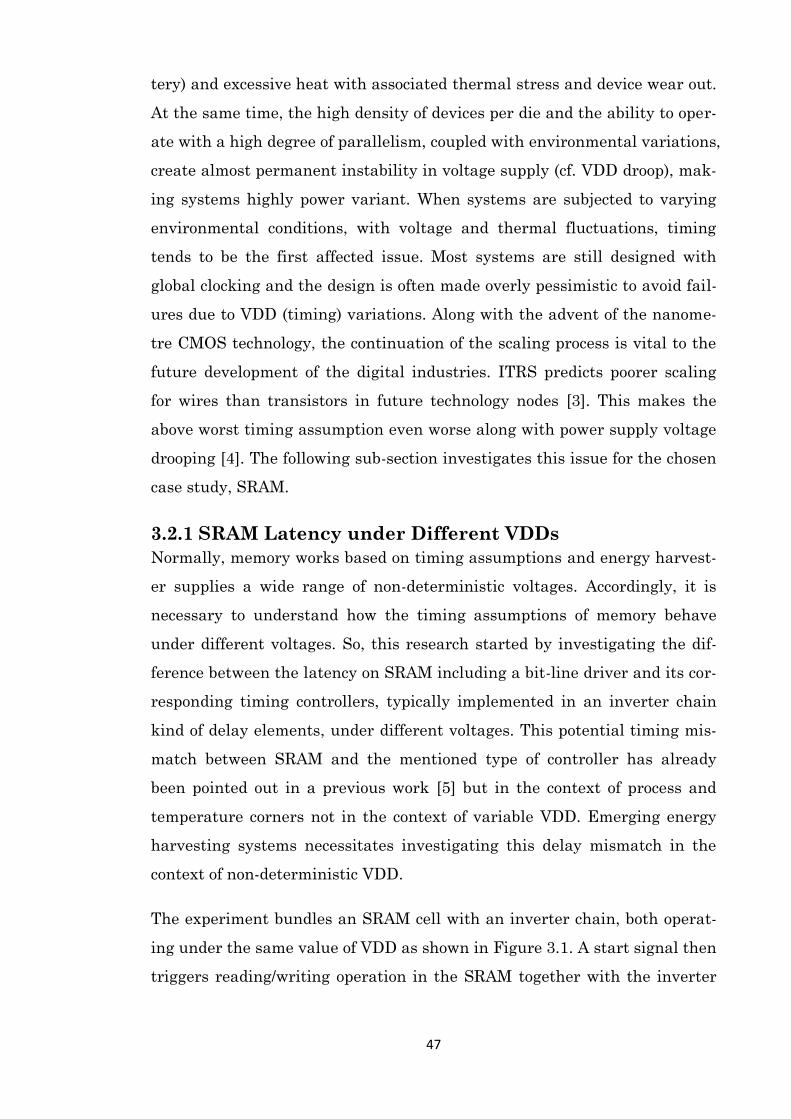
47
tery) and excessive heat with associated thermal stress and device wear out.
At the same time, the high density of devices per die and the ability to oper-
ate with a high degree of parallelism, coupled with environmental variations,
create almost permanent instability in voltage supply (cf. VDD droop), mak-
ing systems highly power variant. When systems are subjected to varying
environmental conditions, with voltage and thermal fluctuations, timing
tends to be the first affected issue. Most systems are still designed with
global clocking and the design is often made overly pessimistic to avoid fail-
ures due to VDD (timing) variations. Along with the advent of the nanome-
tre CMOS technology, the continuation of the scaling process is vital to the
future development of the digital industries. ITRS predicts poorer scaling
for wires than transistors in future technology nodes [3]. This makes the
above worst timing assumption even worse along with power supply voltage
drooping [4]. The following sub-section investigates this issue for the chosen
case study, SRAM.
3.2.1 SRAM Latency under Different VDDs
Normally, memory works based on timing assumptions and energy harvest-
er supplies a wide range of non-deterministic voltages. Accordingly, it is
necessary to understand how the timing assumptions of memory behave
under different voltages. So, this research started by investigating the dif-
ference between the latency on SRAM including a bit-line driver and its cor-
responding timing controllers, typically implemented in an inverter chain
kind of delay elements, under different voltages. This potential timing mis-
match between SRAM and the mentioned type of controller has already
been pointed out in a previous work [5] but in the context of process and
temperature corners not in the context of variable VDD. Emerging energy
harvesting systems necessitates investigating this delay mismatch in the
context of non-deterministic VDD.
The experiment bundles an SRAM cell with an inverter chain, both operat-
ing under the same value of VDD as shown in Figure 3.1. A start signal then
triggers reading/writing operation in the SRAM together with the inverter
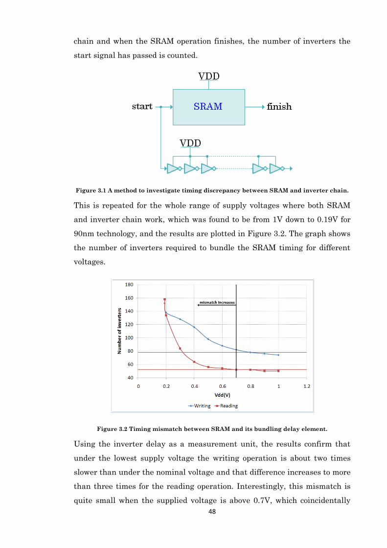
48
chain and when the SRAM operation finishes, the number of inverters the
start signal has passed is counted.
Figure 3.1 A method to investigate timing discrepancy between SRAM and inverter chain.
This is repeated for the whole range of supply voltages where both SRAM
and inverter chain work, which was found to be from 1V down to 0.19V for
90nm technology, and the results are plotted in Figure 3.2. The graph shows
the number of inverters required to bundle the SRAM timing for different
voltages.
Figure 3.2 Timing mismatch between SRAM and its bundling delay element.
Using the inverter delay as a measurement unit, the results confirm that
under the lowest supply voltage the writing operation is about two times
slower than under the nominal voltage and that difference increases to more
than three times for the reading operation. Interestingly, this mismatch is
quite small when the supplied voltage is above 0.7V, which coincidentally
49
was the lowest voltage investigated in some of the previous work (e.g. [6])
for the same technology node. In other words, both reading from and writing
to memory become slower at a much higher rate than inverter chains when
the VDD is reduced below 0.7V. Moreover, delay elements, implemented
based on inverters, do not track memory operation delays when both are op-
erating under the same value of supply voltage. This demonstrates that for
the case of wide ranges of VDD, employing standard inverter chains for
memory delay bundling would require precise design time delay characteri-
zation and conservative worst case provisions, which could be above three
times more wasteful.
After these results were published [1], similar research appeared (e.g. [7]).
The case considered in [7] is only the reading operation in 65nm node and it
augmented the experiment here by expanding the bit-lines to include 128
cells, where the data stored in the cells reflect the worst case bit-line leak-
age described in the second chapter. The reading operation in [7] requires
one clock cycle, which assumed to equate the delay of 20 inverters. For such
a case, the clock frequency varies from more than 0.8GHz at 1.2V to 200kHz
at 0.2V, which means the difference is more than eight orders of magnitude.
In conclusion, this experiment [1] confirms that when the VDD varies a
great deal, the most vulnerable metric of memory system is its timing. In
that case, delay bundling cannot benefit from simple chain of basic gates
without sacrificing more than two times of the system resources. Based on
that, the next section discusses the ideal design technique for this challenge
and then tries to find the right solution to address it.
3.3 Methodology and Design Strategy: Power Adaptive
Computing
In the not so long past low power design was targeted merely at the reduc-
tion of capacitance, VDD, and switching activity, whilst maintaining the re-
quired system performance. In many current applications, the design objec-
tives changed to maximizing the performance within the dynamic power
constraints from energy supply and consumption regimes. Such systems can
no longer be simply regarded as low power systems, but rather as power
50
adaptive or power resilient systems. Normally, this kind of system has two
main properties, which are being power efficient not just low power, and has
the ability to work under non deterministic supply voltage (probably with
known range, which tends to be low) that varies over time. Recently, a pos-
sible solution is proposed for this kind of system, coined energy modulated
systems, which takes power and energy as dynamic resources [8]. That is,
when power is not enough, some of the subsystems could either be powered
off or be executed under lower power supplies and whenever power is ade-
quate, systems can provide high performance. This means that all tasks in a
system are managed based on the power resources, performance require-
ments, and thermal constraints. In the scope of this vision, the next subsec-
tion tries to find the right answer to the raised research question.
3.3.1 Self-Timed SRAM
According to the categorization of SRAM circuit design approaches men-
tioned in the previous chapter, the timing issue has to be addressed by a
timing circuit based approach. Hence, the researcher’s methodology for such
a challenge, which agrees with his understanding of the microelectronic sys-
tems roadmap, is to employ handshaking protocols in order to release the
memory system from any timing assumptions and regulate the circuit oper-
ation based on the actual speed of the data flow rather than on any worst
case timing assumptions [9]. In addition, having such a design gives the
management unit of the whole system the opportunity to swap between dif-
ferent operational modes (e.g. high performance, minimum energy, etc.)
while guaranteeing that SRAM will adapt itself for any mode.
Unfortunately, as described in the second chapter, exploring the literature
shows that fully SRAM operation (reading and writing) has not yet benefit-
ed from completion detection. While reading completion detection was im-
plemented in [10, 11], all works either overlooked writing completion detec-
tion [11] or claimed that it is difficult and impractical [10]. Some works re-
quire a reference voltage, to operate the SRAM under wide range of supply
voltage, and assume it is adjustable for different operational conditions [12].
However, in the energy harvesting environment, there might be no stable
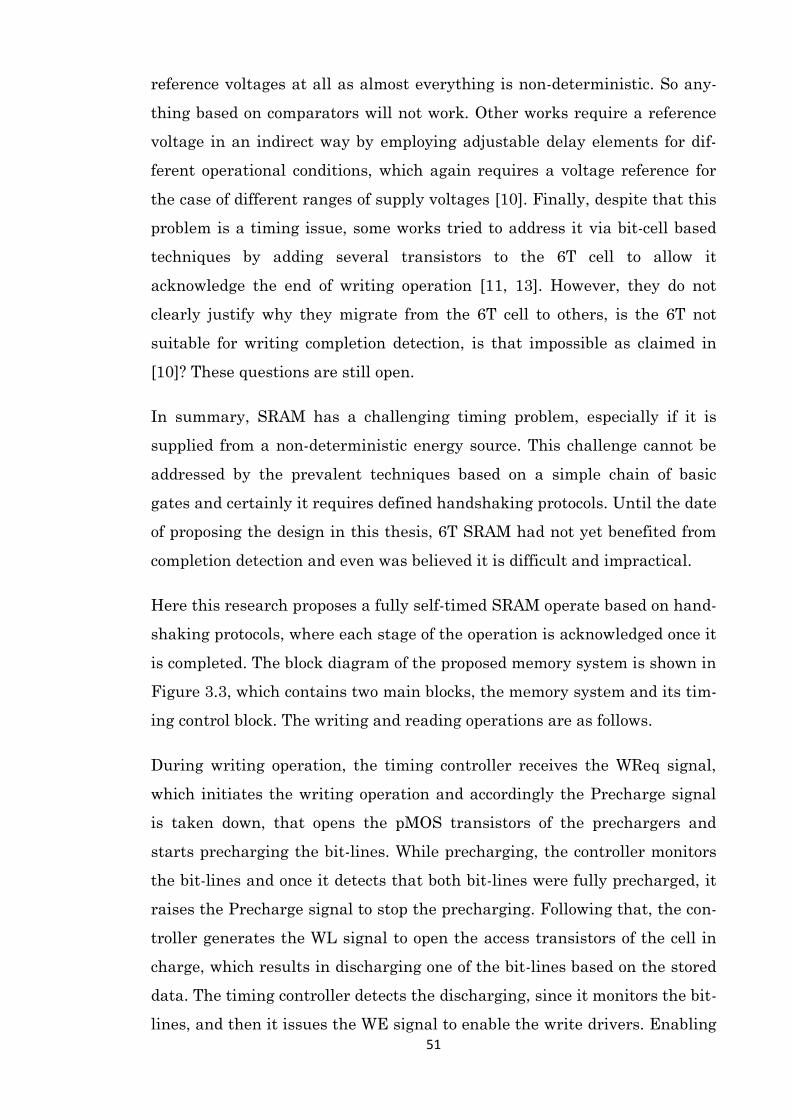
51
reference voltages at all as almost everything is non-deterministic. So any-
thing based on comparators will not work. Other works require a reference
voltage in an indirect way by employing adjustable delay elements for dif-
ferent operational conditions, which again requires a voltage reference for
the case of different ranges of supply voltages [10]. Finally, despite that this
problem is a timing issue, some works tried to address it via bit-cell based
techniques by adding several transistors to the 6T cell to allow it
acknowledge the end of writing operation [11, 13]. However, they do not
clearly justify why they migrate from the 6T cell to others, is the 6T not
suitable for writing completion detection, is that impossible as claimed in
[10]? These questions are still open.
In summary, SRAM has a challenging timing problem, especially if it is
supplied from a non-deterministic energy source. This challenge cannot be
addressed by the prevalent techniques based on a simple chain of basic
gates and certainly it requires defined handshaking protocols. Until the date
of proposing the design in this thesis, 6T SRAM had not yet benefited from
completion detection and even was believed it is difficult and impractical.
Here this research proposes a fully self-timed SRAM operate based on hand-
shaking protocols, where each stage of the operation is acknowledged once it
is completed. The block diagram of the proposed memory system is shown in
Figure 3.3, which contains two main blocks, the memory system and its tim-
ing control block. The writing and reading operations are as follows.
During writing operation, the timing controller receives the WReq signal,
which initiates the writing operation and accordingly the Precharge signal
is taken down, that opens the pMOS transistors of the prechargers and
starts precharging the bit-lines. While precharging, the controller monitors
the bit-lines and once it detects that both bit-lines were fully precharged, it
raises the Precharge signal to stop the precharging. Following that, the con-
troller generates the WL signal to open the access transistors of the cell in
charge, which results in discharging one of the bit-lines based on the stored
data. The timing controller detects the discharging, since it monitors the bit-
lines, and then it issues the WE signal to enable the write drivers. Enabling
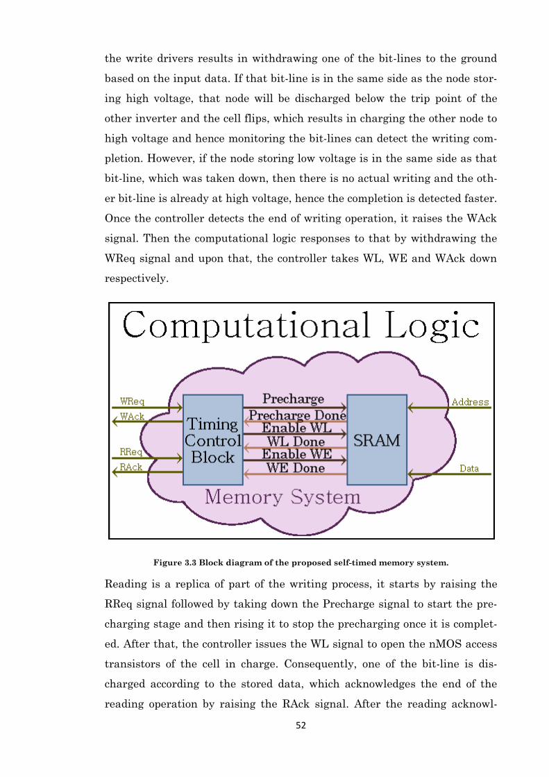
52
the write drivers results in withdrawing one of the bit-lines to the ground
based on the input data. If that bit-line is in the same side as the node stor-
ing high voltage, that node will be discharged below the trip point of the
other inverter and the cell flips, which results in charging the other node to
high voltage and hence monitoring the bit-lines can detect the writing com-
pletion. However, if the node storing low voltage is in the same side as that
bit-line, which was taken down, then there is no actual writing and the oth-
er bit-line is already at high voltage, hence the completion is detected faster.
Once the controller detects the end of writing operation, it raises the WAck
signal. Then the computational logic responses to that by withdrawing the
WReq signal and upon that, the controller takes WL, WE and WAck down
respectively.
Figure 3.3 Block diagram of the proposed self-timed memory system.
Reading is a replica of part of the writing process, it starts by raising the
RReq signal followed by taking down the Precharge signal to start the pre-
charging stage and then rising it to stop the precharging once it is complet-
ed. After that, the controller issues the WL signal to open the nMOS access
transistors of the cell in charge. Consequently, one of the bit-line is dis-
charged according to the stored data, which acknowledges the end of the
reading operation by raising the RAck signal. After the reading acknowl-
53
edgment, the RReq signal is withdrawn by the environment and upon that,
the controller takes the WL and RAck signal down respectively.
These proposed protocols are able to detect the completion of the writing
and reading operation as well as detect the completion of each stage during
writing and reading. For instance, the protocol can inform the surrounding
environment whether the precharging phase finishes or not, whether the
access transistors are opened or not, and so on. The Signal Transition Graph
(STG) specifications of the previously described reading and writing opera-
tion are depicted in Figure 3.4.
Figure 3.4 STG specifications of the reading and writing operations in the 6T cell.
Different circuit design techniques can be employed to implement the STGs
in Figure 3.4. The safest asynchronous circuit is the Delay Insensitive (DI)
one, where the operation works correctly irrespective of latency behaviours
of any component, including logic and wires. Such systems should in general
work correctly under nondeterministic supply voltage variations with aver-
age case performance. However, DI techniques usually require complex cod-
ing (e.g. dual-rail), and have power and size disadvantages [14]. For memory
such as on-chip SRAMs, even small unit penalties will be multiplied to in-
tolerable scales. Moreover, for many applications, DI solutions cannot be
found [15]. Various approximations to true DI have been proposed. For in-
stance, if the delays on wires are assumed to be zero or negligible, systems
can be designed so that any delay variations in the gates do not compromise
correctness. Systems designed in this way are known as Speed Independent
(SI). SI systems tend to be easier and cheaper to design and implement than
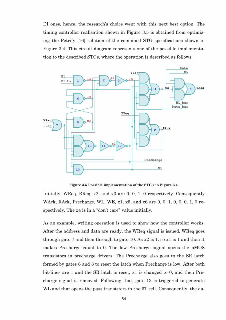
54
DI ones, hence, the research’s choice went with this next best option. The
timing controller realisation shown in Figure 3.5 is obtained from optimiz-
ing the Petrify [16] solution of the combined STG specifications shown in
Figure 3.4. This circuit diagram represents one of the possible implementa-
tion to the described STGs, where the operation is described as follows.
Figure 3.5 Possible implementation of the STG’s in Figure 3.4.
Initially, WReq, RReq, x2, and x3 are 0, 0, 1, 0 respectively. Consequently
WAck, RAck, Precharge, WL, WE, x1, x5, and x6 are 0, 0, 1, 0, 0, 0, 1, 0 re-
spectively. The x4 is in a “don’t care” value initially.
As an example, writing operation is used to show how the controller works.
After the address and data are ready, the WReq signal is issued. WReq goes
through gate 7 and then through to gate 10. As x2 is 1, so x1 is 1 and then it
makes Precharge equal to 0. The low Precharge signal opens the pMOS
transistors in precharge drivers. The Precharge also goes to the SR latch
formed by gates 6 and 8 to reset the latch when Precharge is low. After both
bit-lines are 1 and the SR latch is reset, x1 is changed to 0, and then Pre-
charge signal is removed. Following that, gate 13 is triggered to generate
WL and that opens the pass transistors in the 6T cell. Consequently, the da-
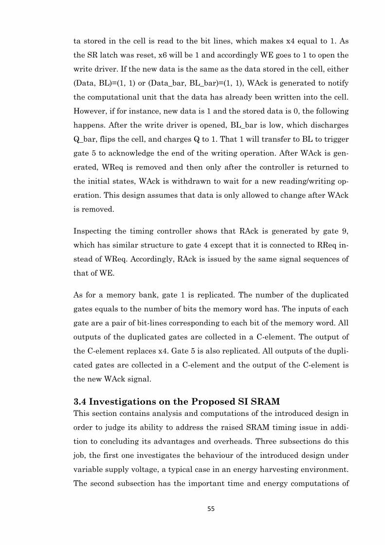
55
ta stored in the cell is read to the bit lines, which makes x4 equal to 1. As
the SR latch was reset, x6 will be 1 and accordingly WE goes to 1 to open the
write driver. If the new data is the same as the data stored in the cell, either
(Data, BL)=(1, 1) or (Data_bar, BL_bar)=(1, 1), WAck is generated to notify
the computational unit that the data has already been written into the cell.
However, if for instance, new data is 1 and the stored data is 0, the following
happens. After the write driver is opened, BL_bar is low, which discharges
Q_bar, flips the cell, and charges Q to 1. That 1 will transfer to BL to trigger
gate 5 to acknowledge the end of the writing operation. After WAck is gen-
erated, WReq is removed and then only after the controller is returned to
the initial states, WAck is withdrawn to wait for a new reading/writing op-
eration. This design assumes that data is only allowed to change after WAck
is removed.
Inspecting the timing controller shows that RAck is generated by gate 9,
which has similar structure to gate 4 except that it is connected to RReq in-
stead of WReq. Accordingly, RAck is issued by the same signal sequences of
that of WE.
As for a memory bank, gate 1 is replicated. The number of the duplicated
gates equals to the number of bits the memory word has. The inputs of each
gate are a pair of bit-lines corresponding to each bit of the memory word. All
outputs of the duplicated gates are collected in a C-element. The output of
the C-element replaces x4. Gate 5 is also replicated. All outputs of the dupli-
cated gates are collected in a C-element and the output of the C-element is
the new WAck signal.
3.4 Investigations on the Proposed SI SRAM
This section contains analysis and computations of the introduced design in
order to judge its ability to address the raised SRAM timing issue in addi-
tion to concluding its advantages and overheads. Three subsections do this
job, the first one investigates the behaviour of the introduced design under
variable supply voltage, a typical case in an energy harvesting environment.
The second subsection has the important time and energy computations of
56
the self-timed SRAM. The last section examines the energy overhead of the
timing controller.
3.4.1 Behaviour of SI SRAM under Variable VDD
Firstly, an SI SRAM is investigated under variable supply voltage, a raw
harvester’s output. In this experiment, the SRAM along with its peripheral
components and timing circuitry are all powered by a sinusoidal voltage
with a frequency of 700kHz and minimum and maximum value of 0.3V and
1V respectively. The experiment consists of writing 0 to the SRAM followed
by a reading operation, then writing 1 to flip the cell followed by a reading
operation. The timing diagrams of all controllers’ critical signals are plotted
in Figure 3.6 in order to examine the functionality. The names in the graph
are the same conventional names employed above.
Figure 3.6 Critical waveforms of self-timed SRAM under variable VDD.
As the VDD changes, the same operation takes different times according to
the voltage at that time. The red and green boxes bound the timing of writ-
ing operation at low and nominal voltages respectively. On the one hand,
the former takes longer time than the latter and at the same time, it runs
faster as the voltage increases. On the other hand, the latter operation gen-
erates the acknowledgement in next to no time and does the task at the
maximum speed of the circuit.
57
The key achievement of this experiment is demonstrating the ability of the
truly and fully self-timed SRAM to remove the timing assumptions required
to operate the circuit at a predefined level of performance. Accordingly, the
circuit adapt itself to regulate the data flow based on the maximum speed it
can provide at each operational condition. Importantly, reflecting upon that
shows a clear opportunity to enable the scheme discussed above, power
adaptive computing. In that scheme, the system has to finish the required
task within the supplied amount of energy even if the performance is very
low and at the same time, it must give the maximum performance whenever
the harvested energy is enough to serve it. Moreover, voltage stability is the
last concern to consider in this scheme as confirmed above.
3.4.2 Timing and Energy Computations
This subsection consists of several experiments, which have the purpose of
measuring the performance and energy of the proposed self-timed SRAM.
Firstly, an SRAM chip is designed in a full-custom manner, by tiling 1024
6T bit-cells in 64 rows and 16 columns to form a bank. Then, the following
peripheral circuits are added, 6x64 decoder, write drivers, prechargers, and
SI-latches. The timing of all included components is managed by the SI con-
troller proposed above.
The memory chip is then tested under a wide range of variable supply volt-
age and found to be fully functional from as low as 0.19V all the way up to
1V. The full functionality here means safe and correct reading, and success-
ful writing. After verifying the functionality of the whole SRAM chip, the
performance and energy calculations are recorded for each value of VDD.
The graphs in Figure 3.7 and Figure 3.8 depict the operation’s delay and its
consumed energy respectively, for different voltage values, where the calcu-
lated metric is for one memory word 16 bits long. Each figure has two
graphs, one for reading coloured in dark red, and one for writing, which is
coloured in green.
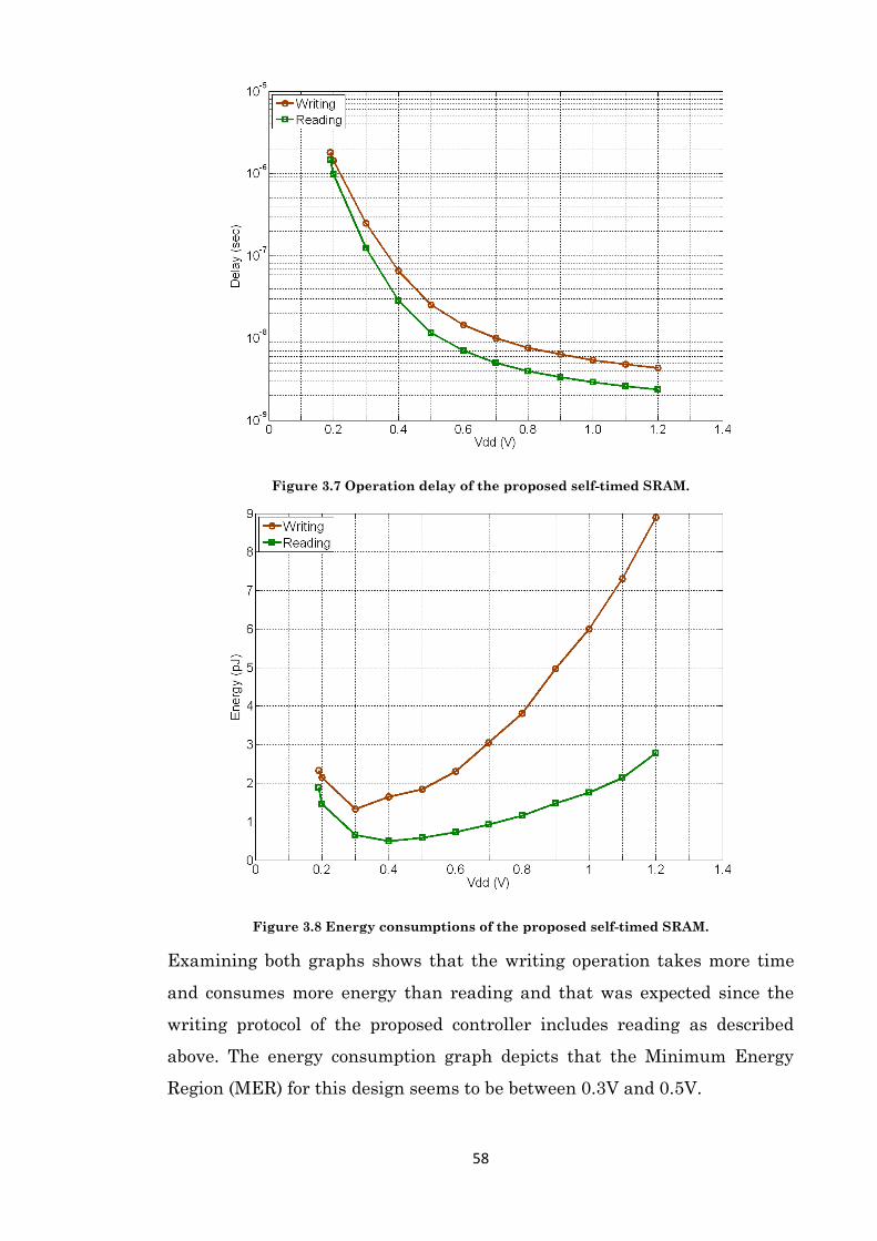
58
Figure 3.7 Operation delay of the proposed self-timed SRAM.
Figure 3.8 Energy consumptions of the proposed self-timed SRAM.
Examining both graphs shows that the writing operation takes more time
and consumes more energy than reading and that was expected since the
writing protocol of the proposed controller includes reading as described
above. The energy consumption graph depicts that the Minimum Energy
Region (MER) for this design seems to be between 0.3V and 0.5V.
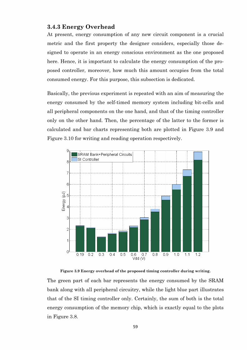
59
3.4.3 Energy Overhead
At present, energy consumption of any new circuit component is a crucial
metric and the first property the designer considers, especially those de-
signed to operate in an energy conscious environment as the one proposed
here. Hence, it is important to calculate the energy consumption of the pro-
posed controller, moreover, how much this amount occupies from the total
consumed energy. For this purpose, this subsection is dedicated.
Basically, the previous experiment is repeated with an aim of measuring the
energy consumed by the self-timed memory system including bit-cells and
all peripheral components on the one hand, and that of the timing controller
only on the other hand. Then, the percentage of the latter to the former is
calculated and bar charts representing both are plotted in Figure 3.9 and
Figure 3.10 for writing and reading operation respectively.
Figure 3.9 Energy overhead of the proposed timing controller during writing.
The green part of each bar represents the energy consumed by the SRAM
bank along with all peripheral circuitry, while the light blue part illustrates
that of the SI timing controller only. Certainly, the sum of both is the total
energy consumption of the memory chip, which is exactly equal to the plots
in Figure 3.8.
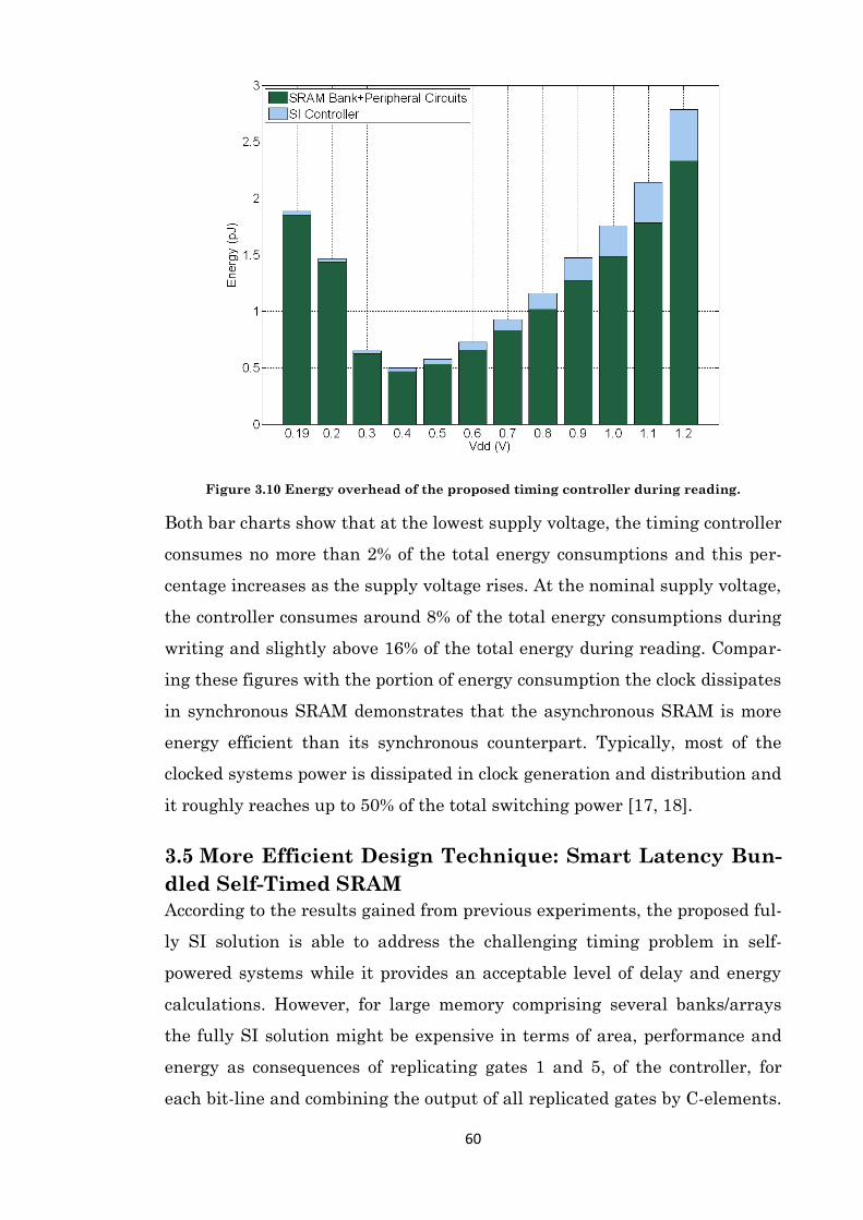
60
Figure 3.10 Energy overhead of the proposed timing controller during reading.
Both bar charts show that at the lowest supply voltage, the timing controller
consumes no more than 2% of the total energy consumptions and this per-
centage increases as the supply voltage rises. At the nominal supply voltage,
the controller consumes around 8% of the total energy consumptions during
writing and slightly above 16% of the total energy during reading. Compar-
ing these figures with the portion of energy consumption the clock dissipates
in synchronous SRAM demonstrates that the asynchronous SRAM is more
energy efficient than its synchronous counterpart. Typically, most of the
clocked systems power is dissipated in clock generation and distribution and
it roughly reaches up to 50% of the total switching power [17, 18].
3.5 More Efficient Design Technique: Smart Latency Bun-
dled Self-Timed SRAM
According to the results gained from previous experiments, the proposed ful-
ly SI solution is able to address the challenging timing problem in self-
powered systems while it provides an acceptable level of delay and energy
calculations. However, for large memory comprising several banks/arrays
the fully SI solution might be expensive in terms of area, performance and
energy as consequences of replicating gates 1 and 5, of the controller, for
each bit-line and combining the output of all replicated gates by C-elements.
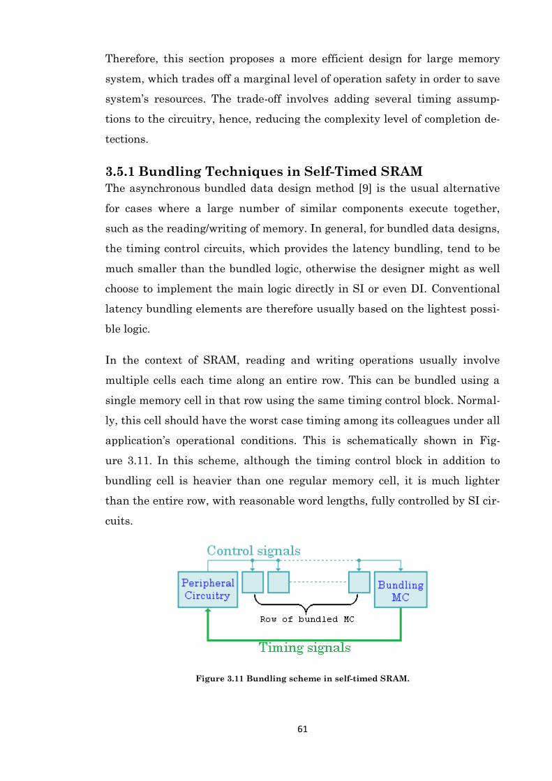
61
Therefore, this section proposes a more efficient design for large memory
system, which trades off a marginal level of operation safety in order to save
system’s resources. The trade-off involves adding several timing assump-
tions to the circuitry, hence, reducing the complexity level of completion de-
tections.
3.5.1 Bundling Techniques in Self-Timed SRAM
The asynchronous bundled data design method [9] is the usual alternative
for cases where a large number of similar components execute together,
such as the reading/writing of memory. In general, for bundled data designs,
the timing control circuits, which provides the latency bundling, tend to be
much smaller than the bundled logic, otherwise the designer might as well
choose to implement the main logic directly in SI or even DI. Conventional
latency bundling elements are therefore usually based on the lightest possi-
ble logic.
In the context of SRAM, reading and writing operations usually involve
multiple cells each time along an entire row. This can be bundled using a
single memory cell in that row using the same timing control block. Normal-
ly, this cell should have the worst case timing among its colleagues under all
application’s operational conditions. This is schematically shown in Fig-
ure 3.11. In this scheme, although the timing control block in addition to
bundling cell is heavier than one regular memory cell, it is much lighter
than the entire row, with reasonable word lengths, fully controlled by SI cir-
cuits.
Figure 3.11 Bundling scheme in self-timed SRAM.
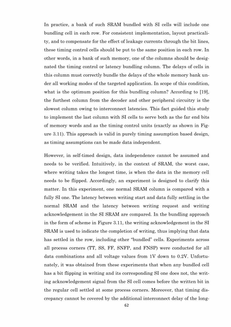
62
In practice, a bank of such SRAM bundled with SI cells will include one
bundling cell in each row. For consistent implementation, layout practicali-
ty, and to compensate for the effect of leakage currents through the bit lines,
these timing control cells should be put to the same position in each row. In
other words, in a bank of such memory, one of the columns should be desig-
nated the timing control or latency bundling column. The delays of cells in
this column must correctly bundle the delays of the whole memory bank un-
der all working modes of the targeted application. In scope of this condition,
what is the optimum position for this bundling column? According to [19],
the furthest column from the decoder and other peripheral circuitry is the
slowest column owing to interconnect latencies. This fact guided this study
to implement the last column with SI cells to serve both as the far end bits
of memory words and as the timing control units (exactly as shown in Fig-
ure 3.11). This approach is valid in purely timing assumption based design,
as timing assumptions can be made data independent.
However, in self-timed design, data independence cannot be assumed and
needs to be verified. Intuitively, in the context of SRAM, the worst case,
where writing takes the longest time, is when the data in the memory cell
needs to be flipped. Accordingly, an experiment is designed to clarify this
matter. In this experiment, one normal SRAM column is compared with a
fully SI one. The latency between writing start and data fully settling in the
normal SRAM and the latency between writing request and writing
acknowledgement in the SI SRAM are compared. In the bundling approach
in the form of scheme in Figure 3.11, the writing acknowledgement in the SI
SRAM is used to indicate the completion of writing, thus implying that data
has settled in the row, including other “bundled” cells. Experiments across
all process corners (TT, SS, FF, SNFP, and FNSP) were conducted for all
data combinations and all voltage values from 1V down to 0.2V. Unfortu-
nately, it was obtained from these experiments that when any bundled cell
has a bit flipping in writing and its corresponding SI one does not, the writ-
ing acknowledgement signal from the SI cell comes before the written bit in
the regular cell settled at some process corners. Moreover, that timing dis-
crepancy cannot be covered by the additional interconnect delay of the long-
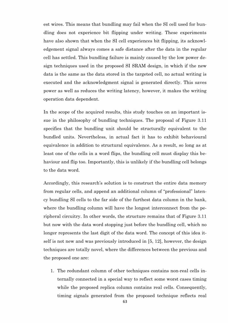
63
est wires. This means that bundling may fail when the SI cell used for bun-
dling does not experience bit flipping under writing. These experiments
have also shown that when the SI cell experiences bit flipping, its acknowl-
edgement signal always comes a safe distance after the data in the regular
cell has settled. This bundling failure is mainly caused by the low power de-
sign techniques used in the proposed SI SRAM design, in which if the new
data is the same as the data stored in the targeted cell, no actual writing is
executed and the acknowledgment signal is generated directly. This saves
power as well as reduces the writing latency, however, it makes the writing
operation data dependent.
In the scope of the acquired results, this study touches on an important is-
sue in the philosophy of bundling techniques. The proposal of Figure 3.11
specifies that the bundling unit should be structurally equivalent to the
bundled units. Nevertheless, in actual fact it has to exhibit behavioural
equivalence in addition to structural equivalence. As a result, so long as at
least one of the cells in a word flips, the bundling cell must display this be-
haviour and flip too. Importantly, this is unlikely if the bundling cell belongs
to the data word.
Accordingly, this research’s solution is to construct the entire data memory
from regular cells, and append an additional column of “professional” laten-
cy bundling SI cells to the far side of the furthest data column in the bank,
where the bundling column will have the longest interconnect from the pe-
ripheral circuitry. In other words, the structure remains that of Figure 3.11
but now with the data word stopping just before the bundling cell, which no
longer represents the last digit of the data word. The concept of this idea it-
self is not new and was previously introduced in [5, 12], however, the design
techniques are totally novel, where the differences between the previous and
the proposed one are:
1. The redundant column of other techniques contains non-real cells in-
ternally connected in a special way to reflect some worst cases timing
while the proposed replica column contains real cells. Consequently,
timing signals generated from the proposed technique reflects real
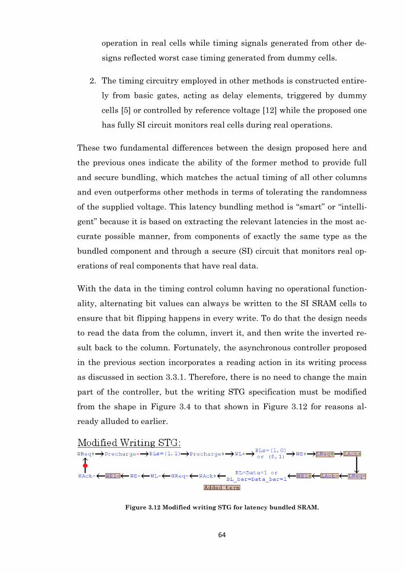
64
operation in real cells while timing signals generated from other de-
signs reflected worst case timing generated from dummy cells.
2. The timing circuitry employed in other methods is constructed entire-
ly from basic gates, acting as delay elements, triggered by dummy
cells [5] or controlled by reference voltage [12] while the proposed one
has fully SI circuit monitors real cells during real operations.
These two fundamental differences between the design proposed here and
the previous ones indicate the ability of the former method to provide full
and secure bundling, which matches the actual timing of all other columns
and even outperforms other methods in terms of tolerating the randomness
of the supplied voltage. This latency bundling method is “smart” or “intelli-
gent” because it is based on extracting the relevant latencies in the most ac-
curate possible manner, from components of exactly the same type as the
bundled component and through a secure (SI) circuit that monitors real op-
erations of real components that have real data.
With the data in the timing control column having no operational function-
ality, alternating bit values can always be written to the SI SRAM cells to
ensure that bit flipping happens in every write. To do that the design needs
to read the data from the column, invert it, and then write the inverted re-
sult back to the column. Fortunately, the asynchronous controller proposed
in the previous section incorporates a reading action in its writing process
as discussed in section 3.3.1. Therefore, there is no need to change the main
part of the controller, but the writing STG specification must be modified
from the shape in Figure 3.4 to that shown in Figure 3.12 for reasons al-
ready alluded to earlier.
Figure 3.12 Modified writing STG for latency bundled SRAM.
65
The STG in Figure 3.4, although correct for use in a system where all cells
are SI, is not suitable for a bundling cell. For instance, if the data being
written into a memory cell is the same as the data already stored in the cell,
according to the STG specification in Figure 3.4, as a round of reading is in-
cluded in the writing process, so the (BL, BL_bar) presents the data stored
in memory. Consequently, the WAck signal will be generated as quickly as
possible, and then the other control signals, such as WL, WE, will be with-
drawn. This maximizes speed and reduces energy consumption, as the actu-
al writing of a bit into the cell is not performed in such a case, but for a bun-
dling cell, this speed up is inappropriate. As a result, the specification for a
bundling cell timing controller is derived from Figure 3.4 and shown in Fig-
ure 3.12. Here a forced writing of a different data bit is used to eliminate
temporal inconsistencies. After the reading action in the writing process has
been completed (indicated by WE+), the data just read (the current stored
data in the memory) is written into a storage, i.e. an SI-latch, by LReq+, and
after this writing to a latch is completed, LAck+ is generated. The resets of
LReq and LAck immediately follow to let the data settle in the storage, and
afterward the complementary of the bit settled in the SI-latch, which is the
inverse of the original data bit, is written back to the cell as new data. This
makes the data being written permanently different from the data previous-
ly stored in the cell. It is worth highlighting that as the data being written
into the latch needs to be stable during write back, the LReq and LAck sig-
nals should be reset before data writing. This is shown in Figure 3.12, as
LAck+ followed by LReq-, and LAck-.
Based on this new STG, the controller must be updated as shown in Fig-
ure 3.13 with additional components. As the augmented requirements do
not affect the main part of the controller, rather than re-synthesizing com-
pletely from Figure 3.12, the researcher chose to retain the design in Fig-
ure 3.5 and manually introduce the additional components to cover the dif-
ference between Figure 3.4 and Figure 3.12. The added logic include a D-
element (sometimes also known as a “sequencer”) to manage the hand-
shakes and an SI-latch to store and invert the bit data. For the D-element,
{WE, WE1} is the master handshake and {LReq, LAck} is the slave one. The
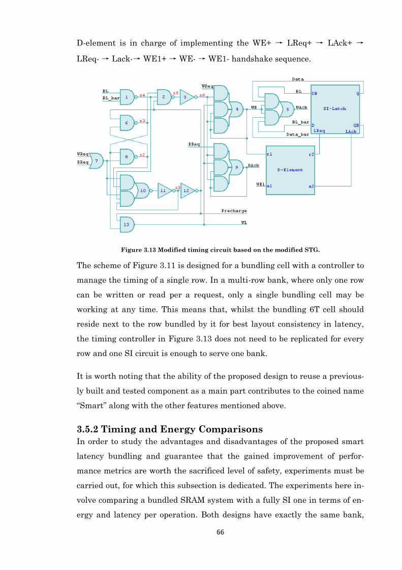
66
D-element is in charge of implementing the WE+ → LReq+ → LAck+ →
LReq- → Lack-→ WE1+ → WE- → WE1- handshake sequence.
Figure 3.13 Modified timing circuit based on the modified STG.
The scheme of Figure 3.11 is designed for a bundling cell with a controller to
manage the timing of a single row. In a multi-row bank, where only one row
can be written or read per a request, only a single bundling cell may be
working at any time. This means that, whilst the bundling 6T cell should
reside next to the row bundled by it for best layout consistency in latency,
the timing controller in Figure 3.13 does not need to be replicated for every
row and one SI circuit is enough to serve one bank.
It is worth noting that the ability of the proposed design to reuse a previous-
ly built and tested component as a main part contributes to the coined name
“Smart” along with the other features mentioned above.
3.5.2 Timing and Energy Comparisons
In order to study the advantages and disadvantages of the proposed smart
latency bundling and guarantee that the gained improvement of perfor-
mance metrics are worth the sacrificed level of safety, experiments must be
carried out, for which this subsection is dedicated. The experiments here in-
volve comparing a bundled SRAM system with a fully SI one in terms of en-
ergy and latency per operation. Both designs have exactly the same bank,

67
decoder, write drivers, prechargers, and SI-latches. However, the SI one us-
es the previous timing controller connected to all bit lines while the bundled
one has a redundant column controlled by the last proposed timing circuitry,
both of which as described earlier. After the full-custom implementation of
both designs, each of them was tested separately and its full functionality is
verified across a wide range of variable VDD, that is from as low as 0.19V
all the way up to 1V. The full functionality means safe and correct reading,
and successful writing. After verifying the functionality of both SRAMs, the
performance and energy calculations are recorded at each value of VDD dur-
ing reading and writing.
The experiments results are plotted in Figure 3.14, Figure 3.15, Figure 3.16,
and Figure 3.17 for writing and reading latencies and energy consumptions
respectively. Each calculated value represents an operation of reading or
writing a 16 bits word. In each graph two bars are plotted at each voltage
level, one is dark blue and the other is light one, both the former and latter
illustrate the performance metrics corresponding to the fully SI and smartly
bundled SRAM respectively.
The obtained results confirm that despite the bundled design having a re-
dundant column, which means more area and switching, it is still able to
save an acceptable amount of energy and timing of the operation across the
whole range of voltage. The graphs conclude that the savings in perfor-
mance metrics during reading is more than that during writing, which oc-
curred because both the latency and energy of writing were worsened by
adding two more components to the controller and an extra stage, as de-
scribed above. The experiments also show that the latency saving decreases
as the supplied voltage increases owing to the fact that as the voltage in-
creases the overhead of combining completion signals from all bit-lines de-
creases. In contrast, the saving in energy increases as the supply voltage in-
creases and that proves the efficiency of the proposed bundling technique in
any energy conscious environment. Certainly, the bigger the bank the more
saving the bundling technique achieves.
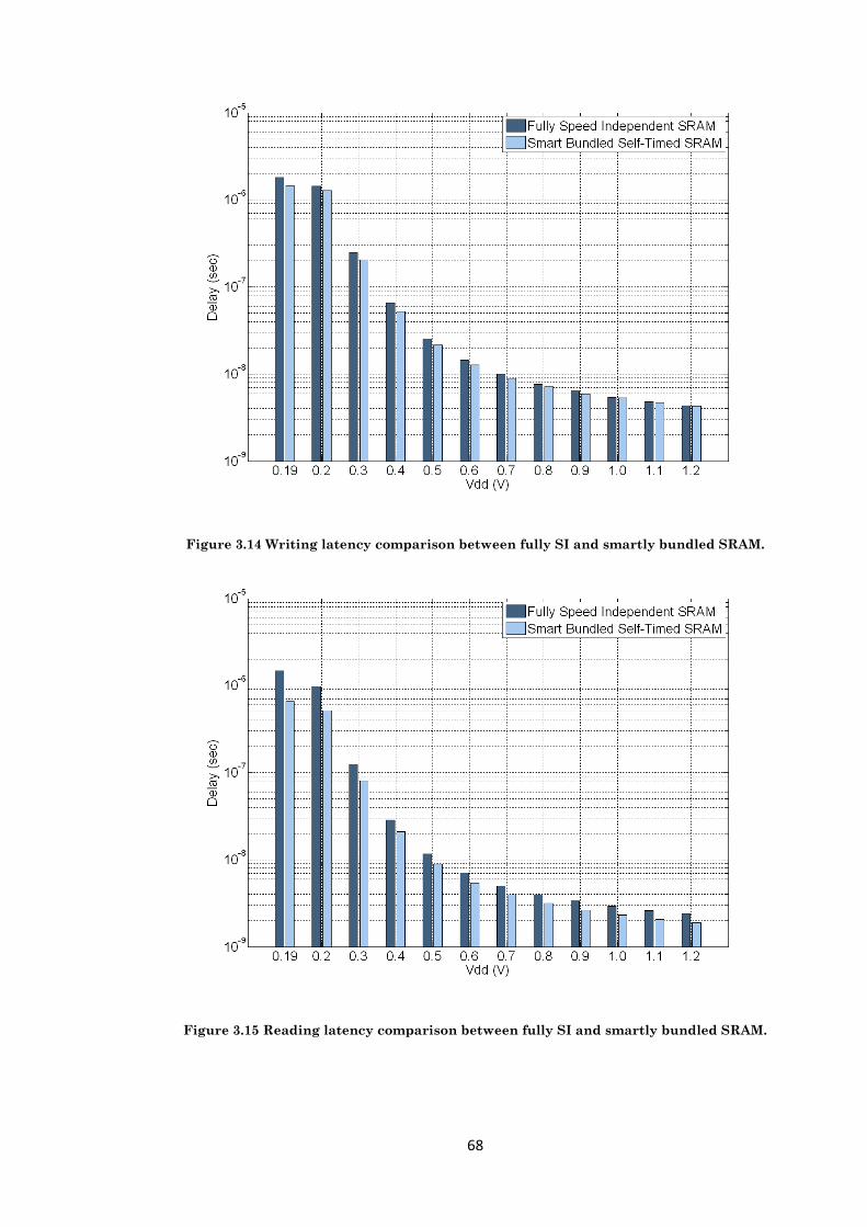
68
Figure 3.14 Writing latency comparison between fully SI and smartly bundled SRAM.
Figure 3.15 Reading latency comparison between fully SI and smartly bundled SRAM.
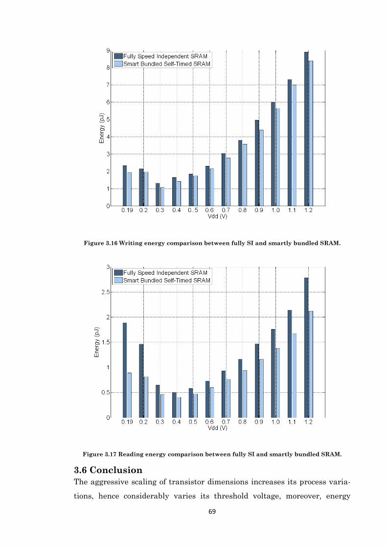
69
Figure 3.16 Writing energy comparison between fully SI and smartly bundled SRAM.
Figure 3.17 Reading energy comparison between fully SI and smartly bundled SRAM.
3.6 Conclusion
The aggressive scaling of transistor dimensions increases its process varia-
tions, hence considerably varies its threshold voltage, moreover, energy
70
scavengers supply nondeterministic voltage to their load. These two main
factors in addition to other reliability issues significantly affect circuit tim-
ing and make it a fuzzy metric during the design time.
Nonetheless, the prevalent techniques of controlling SRAM timing are via
the signals generated from a chain of basic gates. Commonly, in case of a
wide range of operational conditions, reference voltage is generated and em-
ployed to control different delay elements. In both cases, delay elements are
designed according to the worst case cell timing [19], moreover, it is compul-
sory to add a safe margin, during the design time, in order to accommodate
any reliability concerns after fabrication. Unfortunately, this technique
tends to waste a significant portion of system energy and performance,
which exceeds more than twice the required resources, in case of wide range
of supply voltage in the context of SRAM. Furthermore, reference voltage is
impossible to be generated in a nondeterministic environment.
After pointing out the aforementioned issue, this research attempted to pro-
vide a proof of concept of enabling power adaptive computing in the context
of energy harvesting microelectronic systems. Practically, the study sug-
gests regulating the data flow in SRAM based on the actual speed of the cir-
cuits by employing handshaking protocols. This should cancel all timing as-
sumptions and allow the load to adapt itself for whatever is supplied to it.
Importantly, the proposed idea follows the recent ITRS prediction that
asynchrony will increase with the complexity of on-chip systems. Unfortu-
nately, until this research proposed its contribution, SRAM had not yet ben-
efited from fully completion detections operations owing to the challenging
involved in asynchronous design and the belief of some memory designers
that fully and truly handshaking is difficult and impractical for SRAM.
Accordingly, this study provided a method of generating the acknowledg-
ment after completing both reading and writing operation of the SRAM as
well as synthesized that behavioural model in an SI circuits.
The beauty of the synthesized timing controller resides in its ability to re-
port the completion of the whole operation (reading/writing) as well as each
71
stage during the whole operation (precharging, opening access transistors,
enabling write drivers). A basic NAND gate, called Gate 1 (Figure 3.5), is
used to monitor the bit-lines and report the bit-cell activity to the controller.
Therefore, whenever a deadlock happens or the system stops operating, ex-
amining the timing circuits tells what the current state is and what the ex-
isting problem is. Moreover, the ability of this timing controller to operate
the memory under variable VDD highlights the unprecedented feature of
changing the operational modes of the SRAM, i.e. DVS, while it is working
without the need of stopping the operation nor waiting the supply voltage to
settle down. Furthermore, everything is related to and controlled by the
voltage knob only. That is whenever the computing logic requires high per-
formance and does not care about the energy, voltage knob should be rotated
towards high values while the opposite direction means please complete the
task within the supplied amount of energy. In contrast, a synchronous
memory system requires two knobs, voltage and clock, which must be rotat-
ed in opposite directions and with a predefined amount, otherwise, the
whole system fails. Finally, just ignoring the acknowledgment signal of the
timing controller means synchronous SRAM, but with high robustness.
Testing the proposed design showed its ability to address the pointed out
research gap with acceptable timing and energy calculations. Following
that, the study proposed another design based on bundling techniques
which is less safe than the fully SI design but lighter as well, a feature mak-
ing it suitable for large banks.
3.7 References 1. A. Baz, D. Shang, F. Xia, and A. Yakovlev, "Self-Timed SRAM for Energy Harvesting Systems," in In-
tegrated Circuit and System Design. Power and Timing Modeling, Optimization, and Simulation. vol.
6448, R. Leuken and G. Sicard, Eds., ed: Springer Berlin Heidelberg, 2011, pp. 105-115.
2. A. Baz, D. Shang, F. Xia, and A. Yakovlev, "Self-Timed SRAM for Energy Harvesting Systems," Jour-
nal of Low Power Electronics, vol. 7, pp. 274-284, 2011.
3. The International Technology Roadmap for Semiconductors, ITRS Home [online]. Available:
http://www.itrs.net/. 4. V. J. Reddi et al., "Voltage Emergency Prediction: Using Signatures to Reduce Operating Margins,"
in High Performance Computer Architecture, 2009. HPCA 2009. IEEE 15th International Symposium
on, 2009, pp. 18-29.
5. B. S. Amrutur and M. A. Horowitz, "A Replica Technique for Wordline and Sense Control in Low-
Power SRAM's," Solid-State Circuits, IEEE Journal of, vol. 33, pp. 1208-1219, 1998.
6. M. Yamaoka et al., "90-nm Process-Variation Adaptive Embedded SRAM Modules with Power-
Line-Floating Write Technique," Solid-State Circuits, IEEE Journal of, vol. 41, pp. 705-711, 2006.
72
7. J. P. Kulkarni and K. Roy, "Ultralow-Voltage Process-Variation-Tolerant Schmitt-Trigger-Based
SRAM Design," Very Large Scale Integration (VLSI) Systems, IEEE Transactions on, vol. 20, pp. 319-
332, 2012.
8. A. Yakovlev, "Energy-modulated computing," in Design, Automation & Test in Europe Conference
& Exhibition (DATE), 2011, 2011, pp. 1-6.
9. S. Jens and S. Furber, Principles of Asynchronous Circuit Design: A Systems Perspective: Springer,
2001.
10. S. Vincent Wing-Yun, C. Chiu-sing, and C. Cheong-Fat, "A Four-Phase Handshaking Asynchronous
Static RAM Design for Self-Timed Systems," Solid-State Circuits, IEEE Journal of, vol. 34, pp. 90-96,
1999.
11. J. Dama and A. Lines, "GHz Asynchronous SRAM in 65nm," in Asynchronous Circuits and Systems,
2009. ASYNC '09. 15th IEEE Symposium on, 2009, pp. 85-94. 12. C. Meng-Fan, Y. Sue-Meng, and C. Kung-Ting, "Wide VDD Embedded Asynchronous SRAM with
Dual-Mode Self-Timed Technique for Dynamic Voltage Systems," Circuits and Systems I: Regular
Papers, IEEE Transactions on, vol. 56, pp. 1657-1667, 2009. 13. L. S. Nielsen and J. Staunstrup, "Design and Verification of a Self-Timed RAM," in Design Automa-
tion Conference, 1995. Proceedings of the ASP-DAC '95/CHDL '95/VLSI '95., IFIP International Con-
ference on Hardware Description Languages. IFIP International Conference on Very Large Scal,
1995, pp. 751-758.
14. H. Saito et al., "What is the Cost of Delay Insensitivity?," in Computer-Aided Design, 1999. Digest of
Technical Papers. 1999 IEEE/ACM International Conference on, 1999, pp. 316-323.
15. J. M. Alain, "The Limitations to Delay-Insensitivity in Asynchronous Circuits," presented at the Pro-
ceedings of the sixth MIT conference on Advanced research in VLSI, Boston, Massachusetts, USA,
1990.
16. J. Cortadella et al., "Petrify: A Tool for Manipulating Concurrent Specifications and Synthesis of
Asynchronous Controllers," IEICE TRANSACTIONS on Information and Systems, vol. E80-D, pp. 315-
325, 1997.
17. V. G. Oklobdzija, Digital Design and Fabrication: CRC Press, 2007. 18. V. G. Oklobdzija et al., Digital System Clocking: High-Performance and Low-Power Aspects: Wiley,
2005.
19. B. Amelifard, F. Fallah, and M. Pedram, "Leakage Minimization of SRAM Cells in a Dual-Vt and Dual
Tox Technology," Very Large Scale Integration (VLSI) Systems, IEEE Transactions on, vol. 16, pp. 851-
860, 2008.
73
Chapter 4. Design, Fabrication and Testing of Ho-
liSRAM
4.1 Introduction
After proposing a novel design that is able to successfully address the SRAM
timing challenge under nondeterministic power supply, it is the time now to
prove this functionality on real silicon. Accordingly, this chapter is dedicated
for the design, fabrication and testing of the proposed SI SRAM in a chip,
coined HoliSRAM. This name was elected by the research supervisor as a
proof of concept of employing the holistic approach of the project in develop-
ing such a power adaptive SRAM. It is worth highlighting that, while this
chapter tries to cover comprehensively the design and fabrication of the Ho-
liSRAM chip, it, at the same time, avoids reporting some details regarding
the employed technology or the used EDA/CAD tools, which break the Non
Disclosure Agreement (NDA) of using these technologies and/or tools. These
details include but are not limited to cells structures and measurements,
particular design rules and almost all screenshots of the tools. The current
chapter consists of four main sections, where the next one describes the chip
architecture and the reasons behind designing each of its main components.
The third section discusses the design flow of the chip together with the in-
volved challenges. Following that, chip testing and measured results ap-
peared in the fourth section. Finally, the last section concludes the chapter
and highlights the key achievements.
4.2 Chip Architecture
HoliSRAM is a chip designed for the aim of demonstrating the ability of the
self-timed SRAM to work under nondeterministic variable VDD (i.e. Fig-
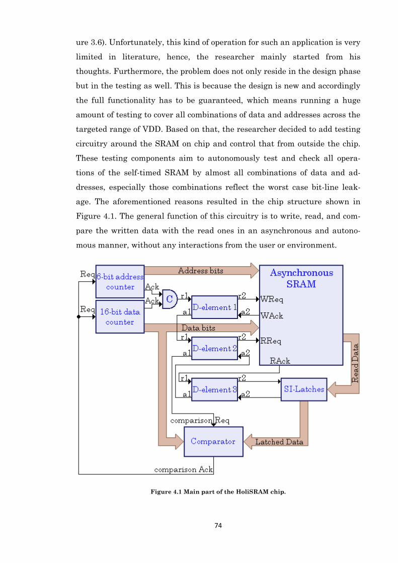
74
ure 3.6). Unfortunately, this kind of operation for such an application is very
limited in literature, hence, the researcher mainly started from his
thoughts. Furthermore, the problem does not only reside in the design phase
but in the testing as well. This is because the design is new and accordingly
the full functionality has to be guaranteed, which means running a huge
amount of testing to cover all combinations of data and addresses across the
targeted range of VDD. Based on that, the researcher decided to add testing
circuitry around the SRAM on chip and control that from outside the chip.
These testing components aim to autonomously test and check all opera-
tions of the self-timed SRAM by almost all combinations of data and ad-
dresses, especially those combinations reflect the worst case bit-line leak-
age. The aforementioned reasons resulted in the chip structure shown in
Figure 4.1. The general function of this circuitry is to write, read, and com-
pare the written data with the read ones in an asynchronous and autono-
mous manner, without any interactions from the user or environment.
Figure 4.1 Main part of the HoliSRAM chip.
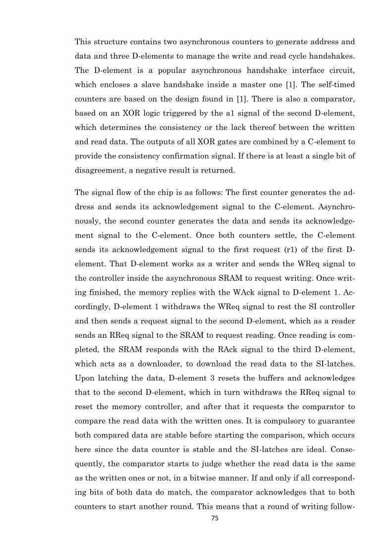
75
This structure contains two asynchronous counters to generate address and
data and three D-elements to manage the write and read cycle handshakes.
The D-element is a popular asynchronous handshake interface circuit,
which encloses a slave handshake inside a master one [1]. The self-timed
counters are based on the design found in [1]. There is also a comparator,
based on an XOR logic triggered by the a1 signal of the second D-element,
which determines the consistency or the lack thereof between the written
and read data. The outputs of all XOR gates are combined by a C-element to
provide the consistency confirmation signal. If there is at least a single bit of
disagreement, a negative result is returned.
The signal flow of the chip is as follows: The first counter generates the ad-
dress and sends its acknowledgement signal to the C-element. Asynchro-
nously, the second counter generates the data and sends its acknowledge-
ment signal to the C-element. Once both counters settle, the C-element
sends its acknowledgement signal to the first request (r1) of the first D-
element. That D-element works as a writer and sends the WReq signal to
the controller inside the asynchronous SRAM to request writing. Once writ-
ing finished, the memory replies with the WAck signal to D-element 1. Ac-
cordingly, D-element 1 withdraws the WReq signal to rest the SI controller
and then sends a request signal to the second D-element, which as a reader
sends an RReq signal to the SRAM to request reading. Once reading is com-
pleted, the SRAM responds with the RAck signal to the third D-element,
which acts as a downloader, to download the read data to the SI-latches.
Upon latching the data, D-element 3 resets the buffers and acknowledges
that to the second D-element, which in turn withdraws the RReq signal to
reset the memory controller, and after that it requests the comparator to
compare the read data with the written ones. It is compulsory to guarantee
both compared data are stable before starting the comparison, which occurs
here since the data counter is stable and the SI-latches are ideal. Conse-
quently, the comparator starts to judge whether the read data is the same
as the written ones or not, in a bitwise manner. If and only if all correspond-
ing bits of both data do match, the comparator acknowledges that to both
counters to start another round. This means that a round of writing follow-
76
ing by reading was correctly performed as the written data was read correct-
ly. If an inconsistency is discovered, however, the entire circuit stops at the
comparator, which allows inspecting the combination of data and operation-
al condition that causes the discrepancy. Towards this aim, the circuitry in
Figure 4.1 is surrounded with several control circuits and numerous storage
elements, which do not appear in the figure and that is outside the scope of
this thesis. The above described operation is illustrated in sequences of sig-
nals captured by the STG in Figure 4.2.
Figure 4.2 STG specification of the SRAM demonstration chip.
At this stage, it is worth highlighting that the proposed design of this test-
ing chip facilitates on-chip self-testing or prototyping where the SI SRAM
may be tested on the same chip with other circuits, reducing the require-
ments of more input and output pins. In addition, the testing may be run at
a wide range of voltage variance, where the tested circuits could distribute a
wide range of speed changes, making it impractical to depend on input and
output pins to extract all the information. In this design, therefore, the test-
ed RAM is surrounded with its entire testing environment on the same piece
of silicon.
Following that, the researcher considered the case of accessing the memory
off the chip for two reasons. The first one is to test the proposed self-timed
SRAM within other systems (e.g. during the holistic demonstration phase of
the EPSRC project). The second goal is to cope with any manufacturing fail-
ure that causes the aforementioned closed loop testing procedure not to op-
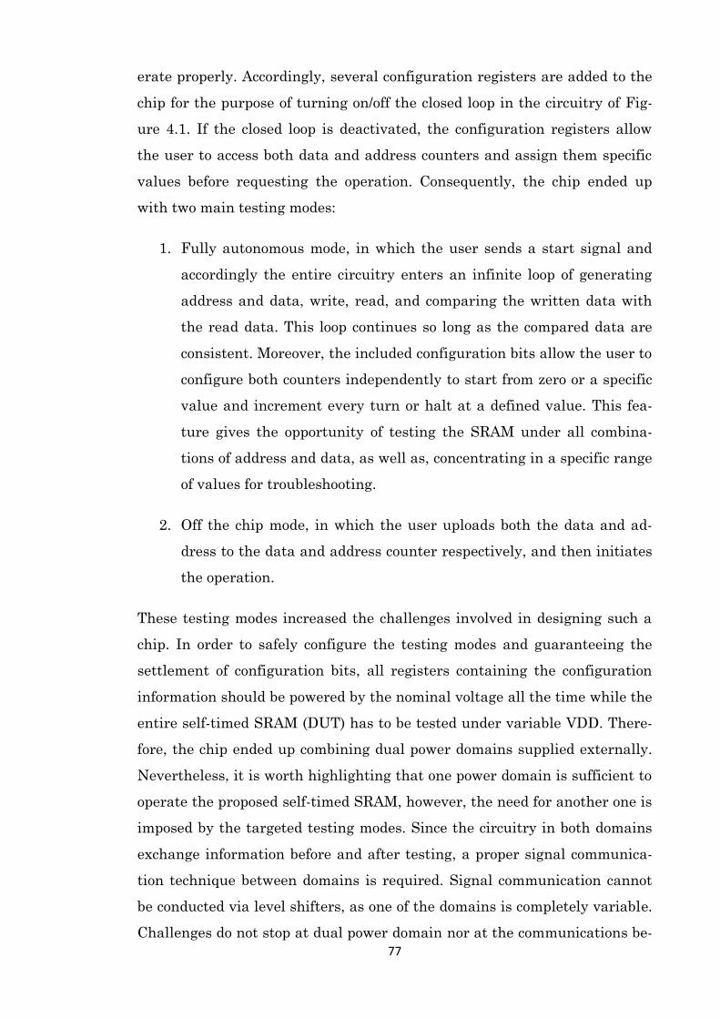
77
erate properly. Accordingly, several configuration registers are added to the
chip for the purpose of turning on/off the closed loop in the circuitry of Fig-
ure 4.1. If the closed loop is deactivated, the configuration registers allow
the user to access both data and address counters and assign them specific
values before requesting the operation. Consequently, the chip ended up
with two main testing modes:
1. Fully autonomous mode, in which the user sends a start signal and
accordingly the entire circuitry enters an infinite loop of generating
address and data, write, read, and comparing the written data with
the read data. This loop continues so long as the compared data are
consistent. Moreover, the included configuration bits allow the user to
configure both counters independently to start from zero or a specific
value and increment every turn or halt at a defined value. This fea-
ture gives the opportunity of testing the SRAM under all combina-
tions of address and data, as well as, concentrating in a specific range
of values for troubleshooting.
2. Off the chip mode, in which the user uploads both the data and ad-
dress to the data and address counter respectively, and then initiates
the operation.
These testing modes increased the challenges involved in designing such a
chip. In order to safely configure the testing modes and guaranteeing the
settlement of configuration bits, all registers containing the configuration
information should be powered by the nominal voltage all the time while the
entire self-timed SRAM (DUT) has to be tested under variable VDD. There-
fore, the chip ended up combining dual power domains supplied externally.
Nevertheless, it is worth highlighting that one power domain is sufficient to
operate the proposed self-timed SRAM, however, the need for another one is
imposed by the targeted testing modes. Since the circuitry in both domains
exchange information before and after testing, a proper signal communica-
tion technique between domains is required. Signal communication cannot
be conducted via level shifters, as one of the domains is completely variable.
Challenges do not stop at dual power domain nor at the communications be-
78
tween them. Moreover, the lack of standard cells to support some essential
components in SRAM and asynchronous design (e.g. prechargers, write
drivers, C-elements, multiplexers), forced the researcher to lay these circuits
out using full-custom designs. Accordingly, the whole design ended up in a
chip requiring dual power domains (nominal voltage for testing circuitry
and variable voltage for DUT) and dual cell design (standard library and
full-custom cells). The next couple of sub-sections are responsible for cover-
ing the design of each part separately together with the integration between
them.
4.2.1 Dual Power Domain Design Phase
Figure 4.3 shows another view of the HoliSRAM chip, it contains two main
parts, which are the variable power domain part and stable power domain
part. The former mainly contains the block diagram in Figure 4.1 in addi-
tion to some auxiliary circuits for buffering and latching.
Figure 4.3 Power domain view of the HoliSRAM chip.
The stable part is much smaller than the variable one and it comprises oth-
er testing facilitating circuitry, which is designed outside the scope of this
thesis, and its main purposes are to allow the user:
1. Configure the chip for a specific testing mode, i.e. full autonomous
mode or off the chip mode.
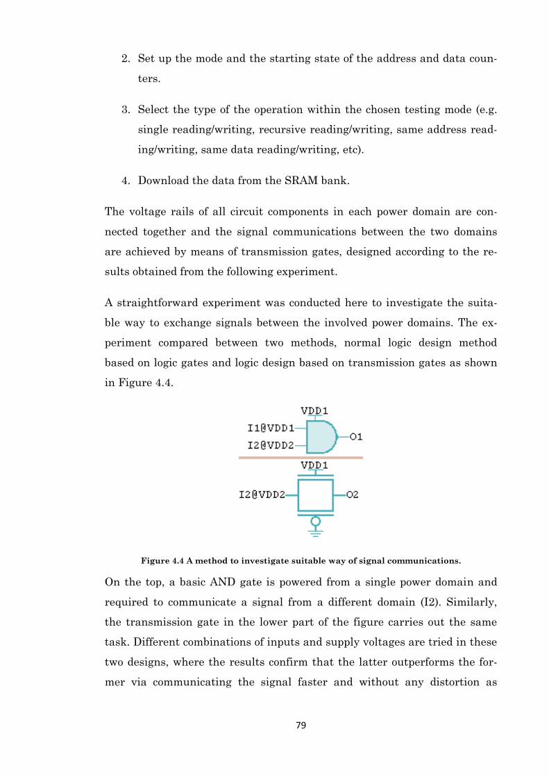
79
2. Set up the mode and the starting state of the address and data coun-
ters.
3. Select the type of the operation within the chosen testing mode (e.g.
single reading/writing, recursive reading/writing, same address read-
ing/writing, same data reading/writing, etc).
4. Download the data from the SRAM bank.
The voltage rails of all circuit components in each power domain are con-
nected together and the signal communications between the two domains
are achieved by means of transmission gates, designed according to the re-
sults obtained from the following experiment.
A straightforward experiment was conducted here to investigate the suita-
ble way to exchange signals between the involved power domains. The ex-
periment compared between two methods, normal logic design method
based on logic gates and logic design based on transmission gates as shown
in Figure 4.4.
Figure 4.4 A method to investigate suitable way of signal communications.
On the top, a basic AND gate is powered from a single power domain and
required to communicate a signal from a different domain (I2). Similarly,
the transmission gate in the lower part of the figure carries out the same
task. Different combinations of inputs and supply voltages are tried in these
two designs, where the results confirm that the latter outperforms the for-
mer via communicating the signal faster and without any distortion as
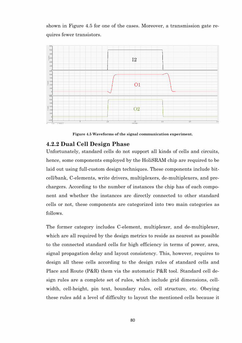
80
shown in Figure 4.5 for one of the cases. Moreover, a transmission gate re-
quires fewer transistors.
Figure 4.5 Waveforms of the signal communication experiment.
4.2.2 Dual Cell Design Phase
Unfortunately, standard cells do not support all kinds of cells and circuits,
hence, some components employed by the HoliSRAM chip are required to be
laid out using full-custom design techniques. These components include bit-
cell/bank, C-elements, write drivers, multiplexers, de-multiplexers, and pre-
chargers. According to the number of instances the chip has of each compo-
nent and whether the instances are directly connected to other standard
cells or not, these components are categorized into two main categories as
follows.
The former category includes C-element, multiplexer, and de-multiplexer,
which are all required by the design metrics to reside as nearest as possible
to the connected standard cells for high efficiency in terms of power, area,
signal propagation delay and layout consistency. This, however, requires to
design all these cells according to the design rules of standard cells and
Place and Route (P&R) them via the automatic P&R tool. Standard cell de-
sign rules are a complete set of rules, which include grid dimensions, cell-
width, cell-height, pin text, boundary rules, cell structure, etc. Obeying
these rules add a level of difficulty to layout the mentioned cells because it

81
requires combining the design rules of the standard cell with those of the
employed technology itself.
The latter category includes bit-cell, bank, precharger and write driver. All
these cells are either not directly connected to the standard cells or connect-
ed but are repeated a few times. This design condition gives those cells more
freedom about where to reside in the design and the required design tech-
nique.
4.3 Chip Design Flow
The previous section discussed how the researcher shaped up the chip archi-
tecture and structure according to the testing modes he targeted along with
the design techniques and rules involved in each part of the chip. Therefore,
it is the time now to start the real design flow, towards that this section is
dedicated.
Firstly, the researcher started by designing the transistor level of the full-
custom cells, following that, he combines the cells he designed with other
standard cell components to form the main circuitry of the chip (e.g. decod-
er, SI timing controller, etc.). After that, he compiled all circuits and compo-
nents into one schematic file that contains two main parts each powered
separately as described earlier.
Before laying out the layers of the obtained schematic file, it is crucial to ex-
amine the operation of the whole chip under the nominal operational condi-
tions as well as under the effect of process variations. This step would help
in guaranteeing the functionality of the chip after fabrication along with its
operational limits. The following subsection covers the experiments and ob-
tained simulation results in more details.
4.3.1 Results of Chip Simulation
Simulating the design in Figure 4.1 confirms its functionality according to
the design goals and testing strategies as depicted in Figure 4.6. The timing
waveforms show that the internal circuits issue the WReq signal, after gen-
erating the address and data as requested, and then hand the job over to the
SI timing controller. The timing controller achieves its job by generating the
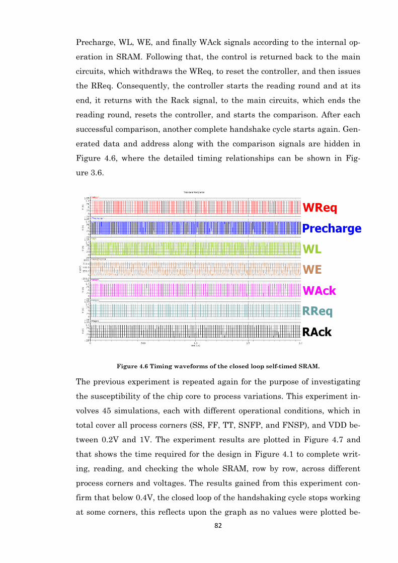
82
Precharge, WL, WE, and finally WAck signals according to the internal op-
eration in SRAM. Following that, the control is returned back to the main
circuits, which withdraws the WReq, to reset the controller, and then issues
the RReq. Consequently, the controller starts the reading round and at its
end, it returns with the Rack signal, to the main circuits, which ends the
reading round, resets the controller, and starts the comparison. After each
successful comparison, another complete handshake cycle starts again. Gen-
erated data and address along with the comparison signals are hidden in
Figure 4.6, where the detailed timing relationships can be shown in Fig-
ure 3.6.
Figure 4.6 Timing waveforms of the closed loop self-timed SRAM.
The previous experiment is repeated again for the purpose of investigating
the susceptibility of the chip core to process variations. This experiment in-
volves 45 simulations, each with different operational conditions, which in
total cover all process corners (SS, FF, TT, SNFP, and FNSP), and VDD be-
tween 0.2V and 1V. The experiment results are plotted in Figure 4.7 and
that shows the time required for the design in Figure 4.1 to complete writ-
ing, reading, and checking the whole SRAM, row by row, across different
process corners and voltages. The results gained from this experiment con-
firm that below 0.4V, the closed loop of the handshaking cycle stops working
at some corners, this reflects upon the graph as no values were plotted be-
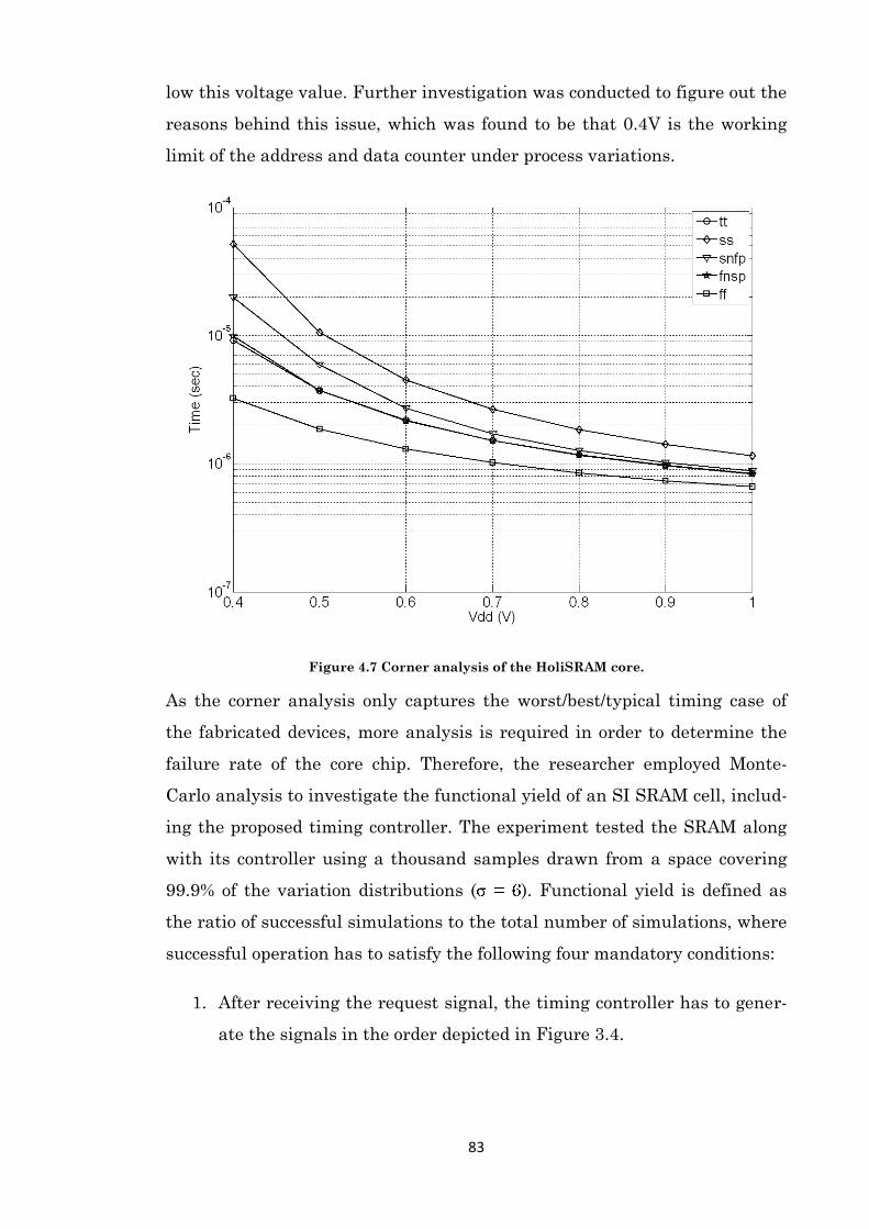
83
low this voltage value. Further investigation was conducted to figure out the
reasons behind this issue, which was found to be that 0.4V is the working
limit of the address and data counter under process variations.
Figure 4.7 Corner analysis of the HoliSRAM core.
As the corner analysis only captures the worst/best/typical timing case of
the fabricated devices, more analysis is required in order to determine the
failure rate of the core chip. Therefore, the researcher employed Monte-
Carlo analysis to investigate the functional yield of an SI SRAM cell, includ-
ing the proposed timing controller. The experiment tested the SRAM along
with its controller using a thousand samples drawn from a space covering
99.9% of the variation distributions ( ). Functional yield is defined as
the ratio of successful simulations to the total number of simulations, where
successful operation has to satisfy the following four mandatory conditions:
1. After receiving the request signal, the timing controller has to gener-
ate the signals in the order depicted in Figure 3.4.
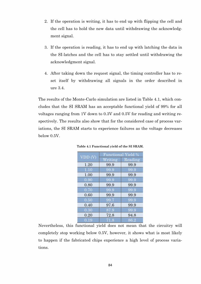
84
2. If the operation is writing, it has to end up with flipping the cell and
the cell has to hold the new data until withdrawing the acknowledg-
ment signal.
3. If the operation is reading, it has to end up with latching the data in
the SI-latches and the cell has to stay settled until withdrawing the
acknowledgment signal.
4. After taking down the request signal, the timing controller has to re-
set itself by withdrawing all signals in the order described in
ure 3.4.
The results of the Monte-Carlo simulation are listed in Table 4.1, which con-
cludes that the SI SRAM has an acceptable functional yield of 99% for all
voltages ranging from 1V down to 0.3V and 0.5V for reading and writing re-
spectively. The results also show that for the considered case of process var-
iations, the SI SRAM starts to experience failures as the voltage decreases
below 0.5V.
Table 4.1 Functional yield of the SI SRAM.
VDD (V) Functional Yield %
Writing Reading
1.20 99.9 99.9
1.10 99.9 99.9
1.00 99.9 99.9
0.90 99.9 99.9
0.80 99.9 99.9
0.70 99.9 99.9
0.60 99.9 99.9
0.50 99.7 99.9
0.40 97.6 99.9
0.30 87.9 99.9
0.20 72.8 94.8
0.19 71.8 86.2
Nevertheless, this functional yield does not mean that the circuitry will
completely stop working below 0.5V, however, it shows what is most likely
to happen if the fabricated chips experience a high level of process varia-
tions.
85
In conclusion, the proposed chip circuitry confirmed the ability to meet the
design goals and testing strategies with an acceptable yield and worst case
analysis and that means full functionality between 100% and 42% of the
nominal voltage and partial functionality below that. This result suggests
taping the chip out, accordingly, the next subsection covers the process of
converting the final schematic developed in this section to real silicon lay-
ers, fully described in the Graphic Database System II (GDSII) file and
ready for fabrication [2].
4.4 Chip Testing
After receiving the chip, the researcher started to prepare for testing accord-
ing to his testing goals explained above. It is the aim of the researchers to
test the fabricated chip in different environments each one was called
stream. Stream I involved examining the functionality of the chip using all
possible testing modes and procedures via an FPGA. Stream II includes
demonstrating the functionality in a portable board by the means of a mi-
crocontroller, in which the user can interact with the SI SRAM via a devel-
oped program interface. It is worth mentioning that stream II is the one in-
volved in this thesis, more information about the demonstration can be
found in the project website: http://www.holistic.ecs.soton.ac.uk/
4.4.1 Stream II Demonstration: a Portable HoliSRAM Box
The main aim of the stream II demonstration is to demonstrate the full
functionality of the self-timed SRAM without equipping any testing instru-
ments, only a laptop suffices.
Figure 4.8 depicts the system diagram of stream II demonstration, which
involves designing the required logic to demonstrate the functionality of the
HoliSRAM chip in a portable box the size of A5 paper.
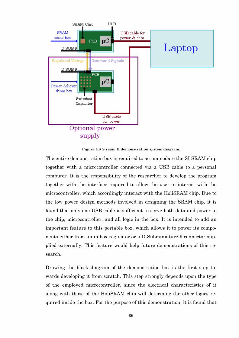
86
Figure 4.8 Stream II demonstration system diagram.
The entire demonstration box is required to accommodate the SI SRAM chip
together with a microcontroller connected via a USB cable to a personal
computer. It is the responsibility of the researcher to develop the program
together with the interface required to allow the user to interact with the
microcontroller, which accordingly interact with the HoliSRAM chip. Due to
the low power design methods involved in designing the SRAM chip, it is
found that only one USB cable is sufficient to serve both data and power to
the chip, microcontroller, and all logic in the box. It is intended to add an
important feature to this portable box, which allows it to power its compo-
nents either from an in-box regulator or a D-Subminiature-9 connector sup-
plied externally. This feature would help future demonstrations of this re-
search.
Drawing the block diagram of the demonstration box is the first step to-
wards developing it from scratch. This step strongly depends upon the type
of the employed microcontroller, since the electrical characteristics of it
along with those of the HoliSRAM chip will determine the other logics re-
quired inside the box. For the purpose of this demonstration, it is found that
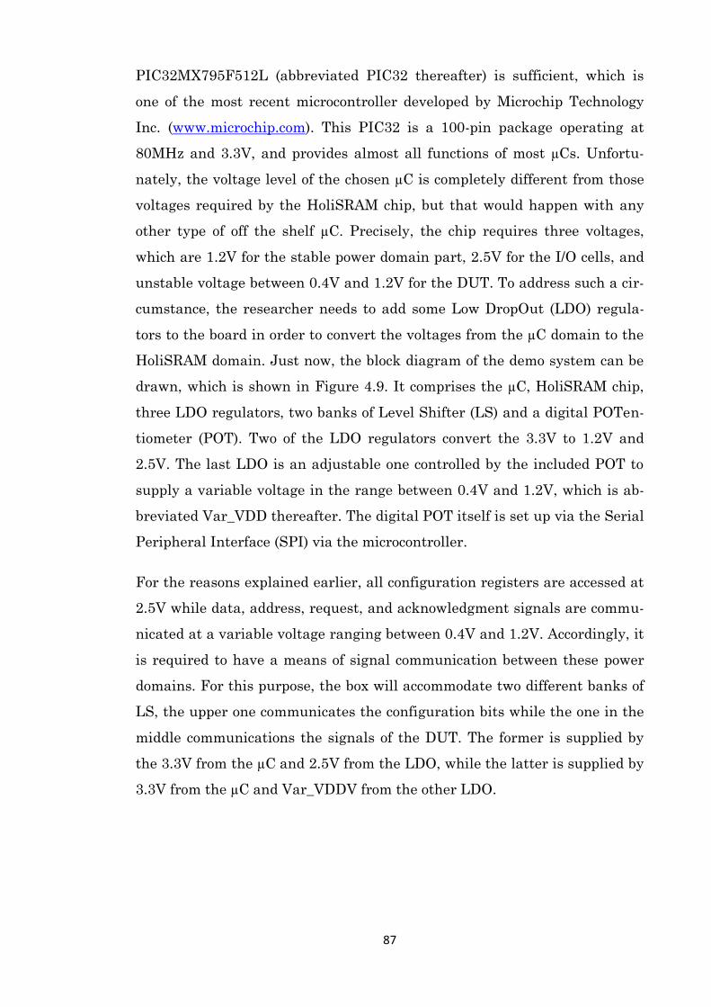
87
PIC32MX795F512L (abbreviated PIC32 thereafter) is sufficient, which is
one of the most recent microcontroller developed by Microchip Technology
Inc. (www.microchip.com). This PIC32 is a 100-pin package operating at
80MHz and 3.3V, and provides almost all functions of most µCs. Unfortu-
nately, the voltage level of the chosen µC is completely different from those
voltages required by the HoliSRAM chip, but that would happen with any
other type of off the shelf µC. Precisely, the chip requires three voltages,
which are 1.2V for the stable power domain part, 2.5V for the I/O cells, and
unstable voltage between 0.4V and 1.2V for the DUT. To address such a cir-
cumstance, the researcher needs to add some Low DropOut (LDO) regula-
tors to the board in order to convert the voltages from the µC domain to the
HoliSRAM domain. Just now, the block diagram of the demo system can be
drawn, which is shown in Figure 4.9. It comprises the µC, HoliSRAM chip,
three LDO regulators, two banks of Level Shifter (LS) and a digital POTen-
tiometer (POT). Two of the LDO regulators convert the 3.3V to 1.2V and
2.5V. The last LDO is an adjustable one controlled by the included POT to
supply a variable voltage in the range between 0.4V and 1.2V, which is ab-
breviated Var_VDD thereafter. The digital POT itself is set up via the Serial
Peripheral Interface (SPI) via the microcontroller.
For the reasons explained earlier, all configuration registers are accessed at
2.5V while data, address, request, and acknowledgment signals are commu-
nicated at a variable voltage ranging between 0.4V and 1.2V. Accordingly, it
is required to have a means of signal communication between these power
domains. For this purpose, the box will accommodate two different banks of
LS, the upper one communicates the configuration bits while the one in the
middle communications the signals of the DUT. The former is supplied by
the 3.3V from the µC and 2.5V from the LDO, while the latter is supplied by
3.3V from the µC and Var_VDDV from the other LDO.
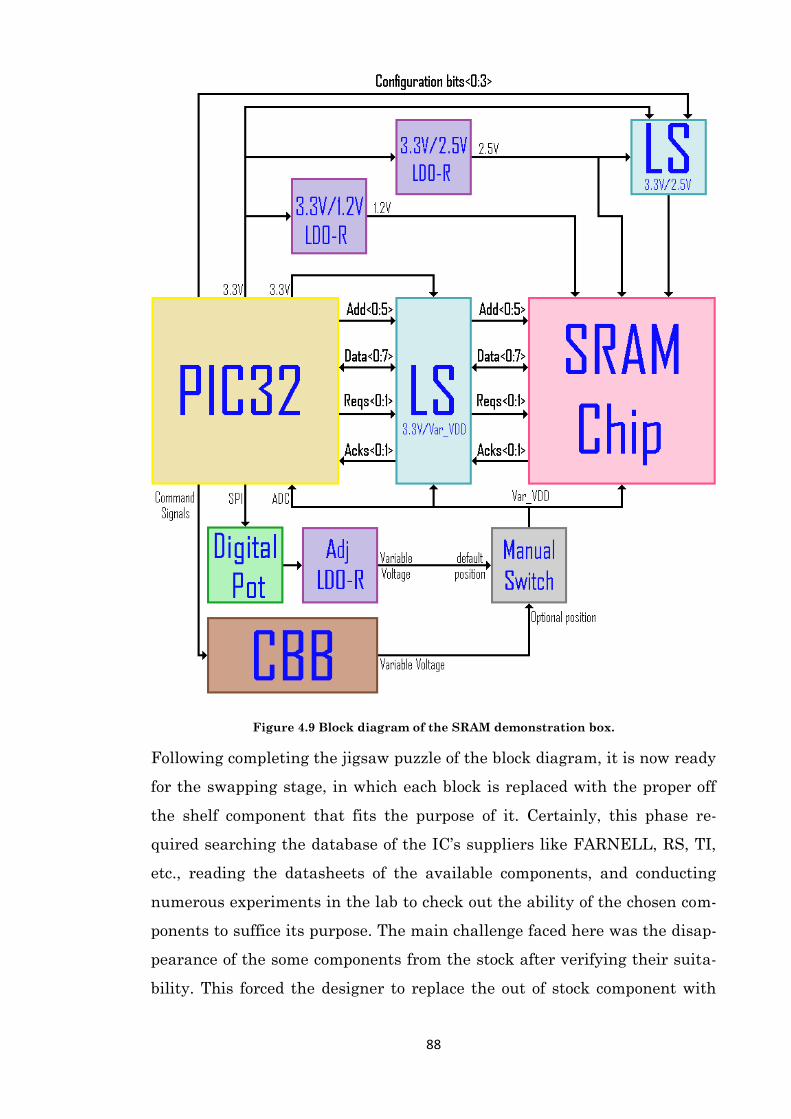
88
Figure 4.9 Block diagram of the SRAM demonstration box.
Following completing the jigsaw puzzle of the block diagram, it is now ready
for the swapping stage, in which each block is replaced with the proper off
the shelf component that fits the purpose of it. Certainly, this phase re-
quired searching the database of the IC’s suppliers like FARNELL, RS, TI,
etc., reading the datasheets of the available components, and conducting
numerous experiments in the lab to check out the ability of the chosen com-
ponents to suffice its purpose. The main challenge faced here was the disap-
pearance of the some components from the stock after verifying their suita-
bility. This forced the designer to replace the out of stock component with
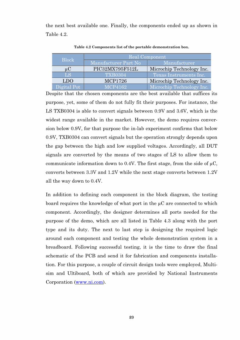
89
the next best available one. Finally, the components ended up as shown in
Table 4.2.
Table 4.2 Components list of the portable demonstration box.
Block Real Component
Manufacturer Part No Manufacturer
µC PIC32MX795F512L Microchip Technology Inc.
LS TXB0304 Texas Instruments Inc.
LDO MCP1726 Microchip Technology Inc.
Digital Pot MCP4162 Microchip Technology Inc.
Despite that the chosen components are the best available that suffices its
purpose, yet, some of them do not fully fit their purposes. For instance, the
LS TXB0304 is able to convert signals between 0.9V and 3.6V, which is the
widest range available in the market. However, the demo requires conver-
sion below 0.9V, for that purpose the in-lab experiment confirms that below
0.9V, TXB0304 can convert signals but the operation strongly depends upon
the gap between the high and low supplied voltages. Accordingly, all DUT
signals are converted by the means of two stages of LS to allow them to
communicate information down to 0.4V. The first stage, from the side of µC,
converts between 3.3V and 1.2V while the next stage converts between 1.2V
all the way down to 0.4V.
In addition to defining each component in the block diagram, the testing
board requires the knowledge of what port in the µC are connected to which
component. Accordingly, the designer determines all ports needed for the
purpose of the demo, which are all listed in Table 4.3 along with the port
type and its duty. The next to last step is designing the required logic
around each component and testing the whole demonstration system in a
breadboard. Following successful testing, it is the time to draw the final
schematic of the PCB and send it for fabrication and components installa-
tion. For this purpose, a couple of circuit design tools were employed, Multi-
sim and Ultiboard, both of which are provided by National Instruments
Corporation (www.ni.com).
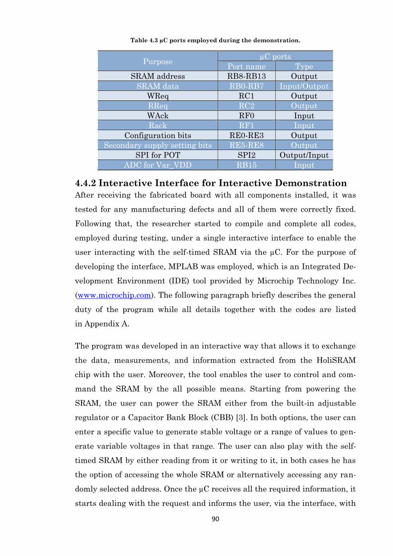
90
Table 4.3 µC ports employed during the demonstration.
Purpose µC ports
Port name Type
SRAM address RB8-RB13 Output
SRAM data RB0-RB7 Input/Output
WReq RC1 Output
RReq RC2 Output
WAck RF0 Input
Rack RF1 Input
Configuration bits RE0-RE3 Output
Secondary supply setting bits RE5-RE8 Output
SPI for POT SPI2 Output/Input
ADC for Var_VDD RB15 Input
4.4.2 Interactive Interface for Interactive Demonstration
After receiving the fabricated board with all components installed, it was
tested for any manufacturing defects and all of them were correctly fixed.
Following that, the researcher started to compile and complete all codes,
employed during testing, under a single interactive interface to enable the
user interacting with the self-timed SRAM via the µC. For the purpose of
developing the interface, MPLAB was employed, which is an Integrated De-
velopment Environment (IDE) tool provided by Microchip Technology Inc.
(www.microchip.com). The following paragraph briefly describes the general
duty of the program while all details together with the codes are listed
in Appendix A.
The program was developed in an interactive way that allows it to exchange
the data, measurements, and information extracted from the HoliSRAM
chip with the user. Moreover, the tool enables the user to control and com-
mand the SRAM by the all possible means. Starting from powering the
SRAM, the user can power the SRAM either from the built-in adjustable
regulator or a Capacitor Bank Block (CBB) [3]. In both options, the user can
enter a specific value to generate stable voltage or a range of values to gen-
erate variable voltages in that range. The user can also play with the self-
timed SRAM by either reading from it or writing to it, in both cases he has
the option of accessing the whole SRAM or alternatively accessing any ran-
domly selected address. Once the µC receives all the required information, it
starts dealing with the request and informs the user, via the interface, with
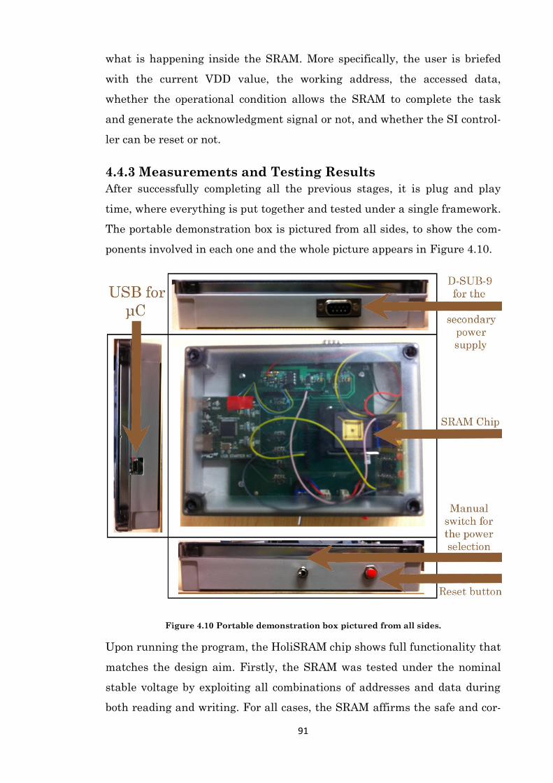
91
what is happening inside the SRAM. More specifically, the user is briefed
with the current VDD value, the working address, the accessed data,
whether the operational condition allows the SRAM to complete the task
and generate the acknowledgment signal or not, and whether the SI control-
ler can be reset or not.
4.4.3 Measurements and Testing Results
After successfully completing all the previous stages, it is plug and play
time, where everything is put together and tested under a single framework.
The portable demonstration box is pictured from all sides, to show the com-
ponents involved in each one and the whole picture appears in Figure 4.10.
Figure 4.10 Portable demonstration box pictured from all sides.
Upon running the program, the HoliSRAM chip shows full functionality that
matches the design aim. Firstly, the SRAM was tested under the nominal
stable voltage by exploiting all combinations of addresses and data during
both reading and writing. For all cases, the SRAM affirms the safe and cor-
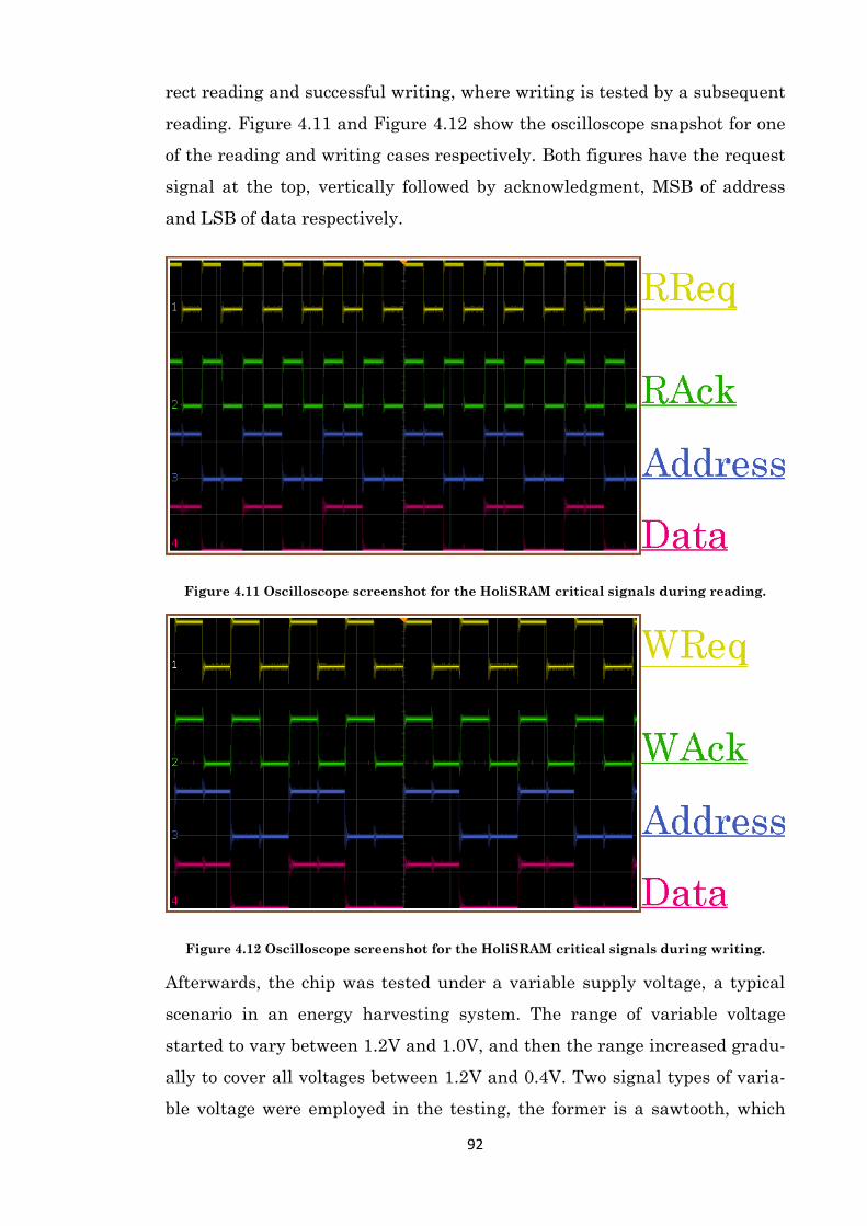
92
rect reading and successful writing, where writing is tested by a subsequent
reading. Figure 4.11 and Figure 4.12 show the oscilloscope snapshot for one
of the reading and writing cases respectively. Both figures have the request
signal at the top, vertically followed by acknowledgment, MSB of address
and LSB of data respectively.
Figure 4.11 Oscilloscope screenshot for the HoliSRAM critical signals during reading.
Figure 4.12 Oscilloscope screenshot for the HoliSRAM critical signals during writing.
Afterwards, the chip was tested under a variable supply voltage, a typical
scenario in an energy harvesting system. The range of variable voltage
started to vary between 1.2V and 1.0V, and then the range increased gradu-
ally to cover all voltages between 1.2V and 0.4V. Two signal types of varia-
ble voltage were employed in the testing, the former is a sawtooth, which
93
appears in Figure 4.13, while the latter is a sinusoidal and it appears in
Figure 4.14. Both figures have the VDD signal at top vertically followed by
WReq, WAck, RReq and RAck signals respectively. The experiment involves
recursive writing, followed by recursive reading, where the data is compared
via the developed tool. The obtained waveforms show two regions of opera-
tions, one between 1V and 0.75V and the other between 0.75V and 0.4V. The
former reflects correct and full functionality of the chip while the latter re-
flects an ambiguous region, where the acknowledgment signals hardly ap-
pear denoted by the gaps in Figure 4.13 and Figure 4.14.
Importantly, these genuine signals, which are extracted from a real piece of
silicon, confirm the ability of the proposed asynchronous SRAM to tolerate
supply voltage variations up to 64% of the nominal value in addition to the
embedded process variations in 90nm technology. This high level of robust-
ness is acquired via regulating the data flow inside the SRAM according to
the actual speed of the circuit, which has a deep gratitude to the proposed
smart completion detection technique. The proposed SI timing controller is
acknowledged as well for its ability to tolerate the delay variations inside its
component in order to generate hazard free signals. In terms of Data Reten-
tion Voltage (DRV), the HoliSRAM chip confirms preserving the data down
to 0.4V at room temperature.
Notably, the real signals highlight an important philosophy behind the pro-
posed design technique of this study, which states that only one knob (i.e.
the supply voltage) is sufficient to control everything. If that knob is rotated
towards high values, it means do the job with the highest performance re-
gardless of the energy consumption. However, if the knob is spun in the op-
posite direction, that means complete the task within the supplied amount
of energy and do not concern the performance. In contrast, in the synchro-
nous counterpart, two knobs are required (i.e. the supplied voltage and
clock) where both must be rotated in the opposite direction with a sensible
amount, which is pre-defined based on the worst case scenario, otherwise
the whole system would certainly fail. The above highlighted philosophy is a
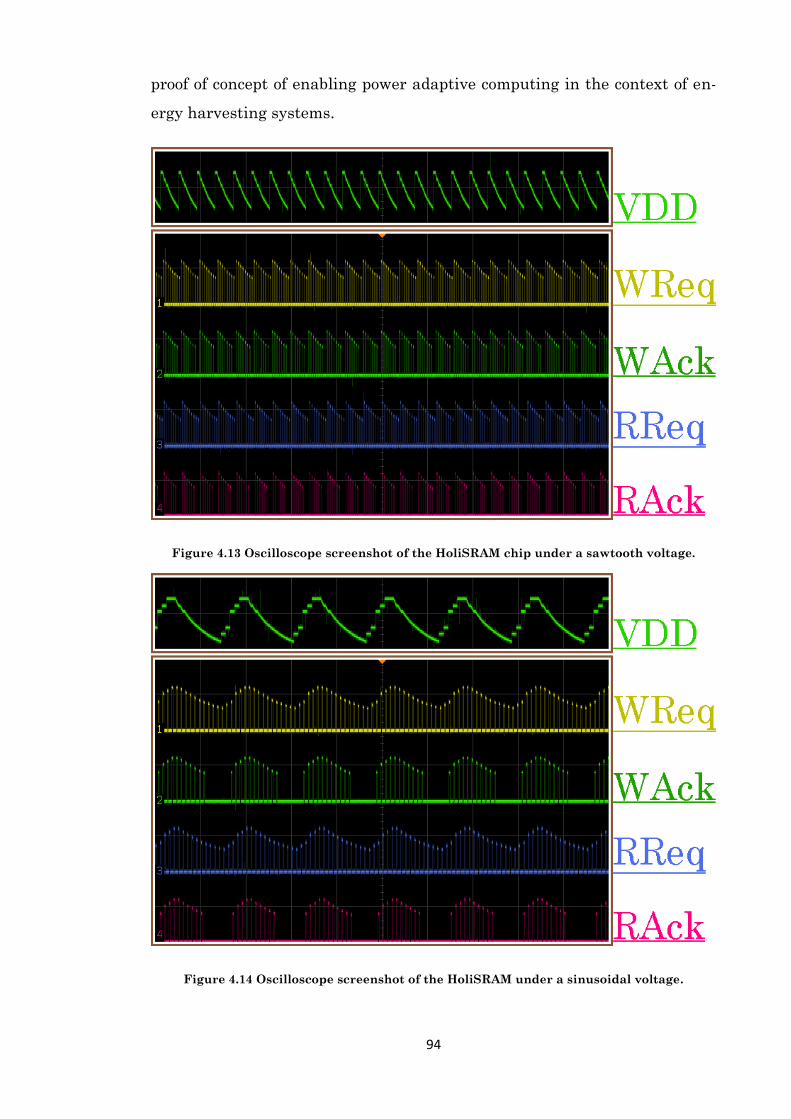
94
proof of concept of enabling power adaptive computing in the context of en-
ergy harvesting systems.
Figure 4.13 Oscilloscope screenshot of the HoliSRAM chip under a sawtooth voltage.
Figure 4.14 Oscilloscope screenshot of the HoliSRAM under a sinusoidal voltage.
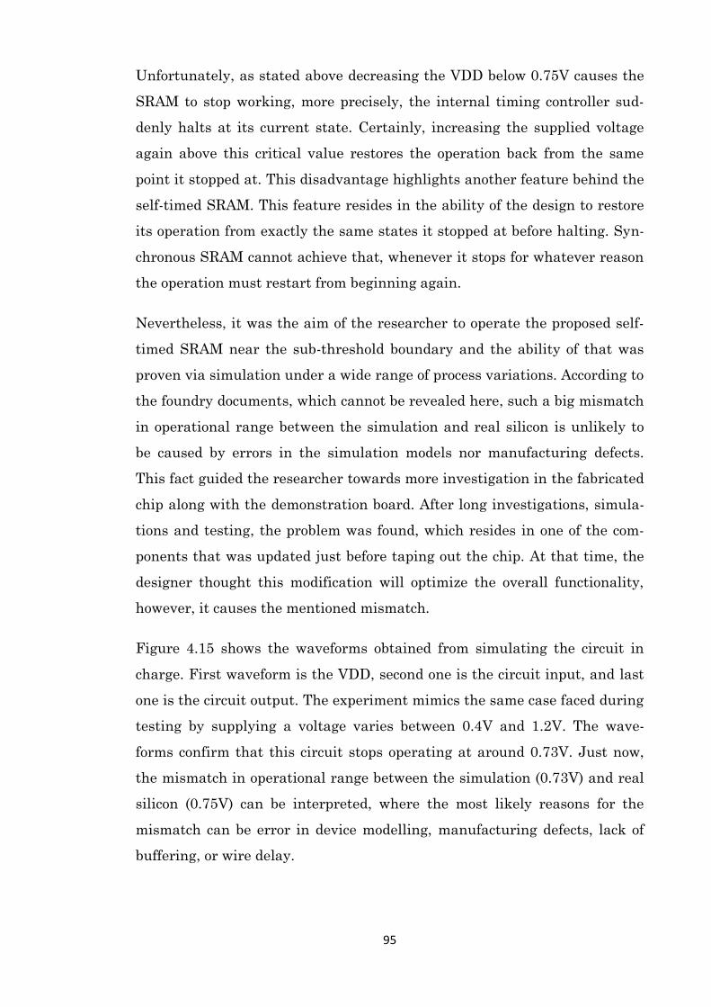
95
Unfortunately, as stated above decreasing the VDD below 0.75V causes the
SRAM to stop working, more precisely, the internal timing controller sud-
denly halts at its current state. Certainly, increasing the supplied voltage
again above this critical value restores the operation back from the same
point it stopped at. This disadvantage highlights another feature behind the
self-timed SRAM. This feature resides in the ability of the design to restore
its operation from exactly the same states it stopped at before halting. Syn-
chronous SRAM cannot achieve that, whenever it stops for whatever reason
the operation must restart from beginning again.
Nevertheless, it was the aim of the researcher to operate the proposed self-
timed SRAM near the sub-threshold boundary and the ability of that was
proven via simulation under a wide range of process variations. According to
the foundry documents, which cannot be revealed here, such a big mismatch
in operational range between the simulation and real silicon is unlikely to
be caused by errors in the simulation models nor manufacturing defects.
This fact guided the researcher towards more investigation in the fabricated
chip along with the demonstration board. After long investigations, simula-
tions and testing, the problem was found, which resides in one of the com-
ponents that was updated just before taping out the chip. At that time, the
designer thought this modification will optimize the overall functionality,
however, it causes the mentioned mismatch.
Figure 4.15 shows the waveforms obtained from simulating the circuit in
charge. First waveform is the VDD, second one is the circuit input, and last
one is the circuit output. The experiment mimics the same case faced during
testing by supplying a voltage varies between 0.4V and 1.2V. The wave-
forms confirm that this circuit stops operating at around 0.73V. Just now,
the mismatch in operational range between the simulation (0.73V) and real
silicon (0.75V) can be interpreted, where the most likely reasons for the
mismatch can be error in device modelling, manufacturing defects, lack of
buffering, or wire delay.
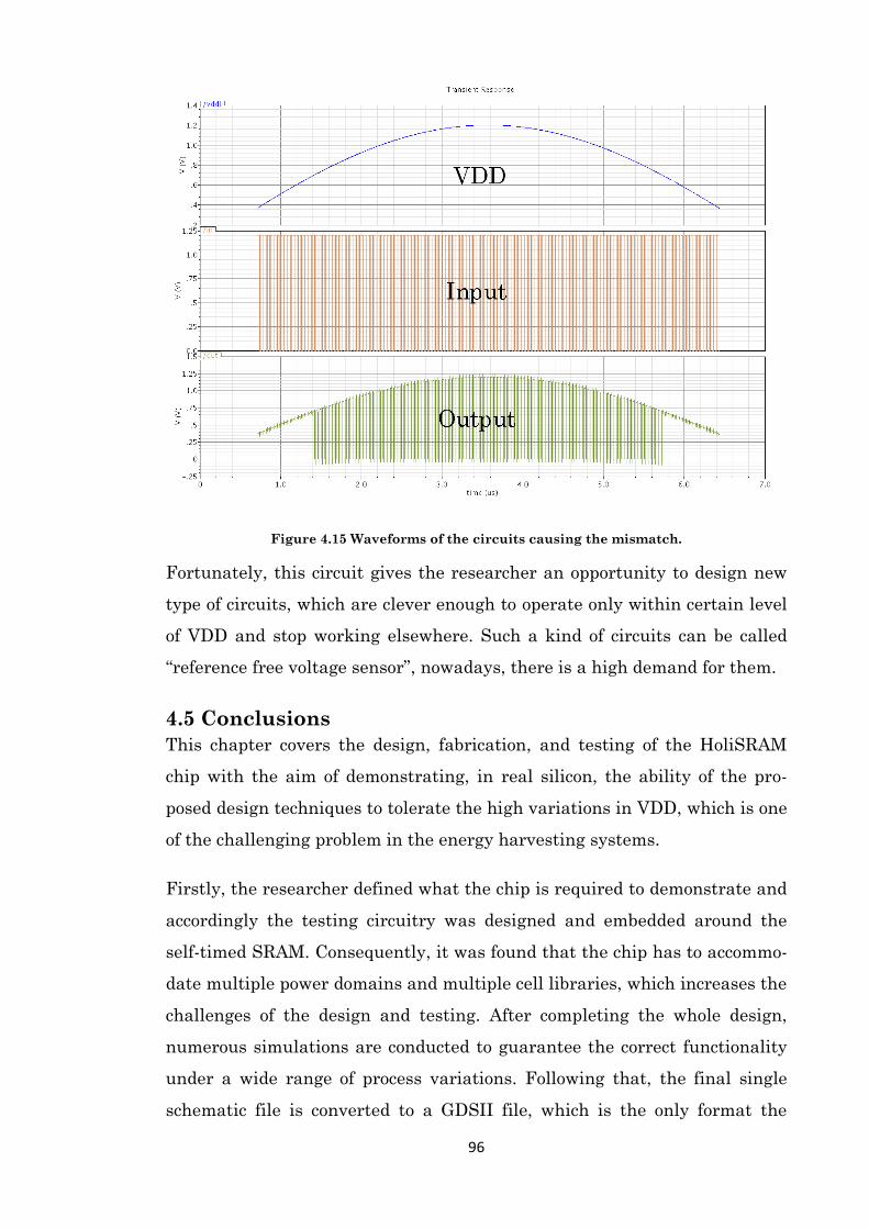
96
Figure 4.15 Waveforms of the circuits causing the mismatch.
Fortunately, this circuit gives the researcher an opportunity to design new
type of circuits, which are clever enough to operate only within certain level
of VDD and stop working elsewhere. Such a kind of circuits can be called
“reference free voltage sensor”, nowadays, there is a high demand for them.
4.5 Conclusions
This chapter covers the design, fabrication, and testing of the HoliSRAM
chip with the aim of demonstrating, in real silicon, the ability of the pro-
posed design techniques to tolerate the high variations in VDD, which is one
of the challenging problem in the energy harvesting systems.
Firstly, the researcher defined what the chip is required to demonstrate and
accordingly the testing circuitry was designed and embedded around the
self-timed SRAM. Consequently, it was found that the chip has to accommo-
date multiple power domains and multiple cell libraries, which increases the
challenges of the design and testing. After completing the whole design,
numerous simulations are conducted to guarantee the correct functionality
under a wide range of process variations. Following that, the final single
schematic file is converted to a GDSII file, which is the only format the
97
foundry understands, via a very long process and by employing several
tools.
After sending the chip for fabrication, the process of testing preparation
started. It was planned to involve the chip in several testing and demonstra-
tion streams. This thesis concentrates on only one of them, which is called
stream II. This stream aims to design a portable demonstration system for
the HoliSRAM chip that allows interacting with the self-timed SRAM with-
out equipping any other testing instruments, only a laptop suffices. The
demonstration involves circuit design, fabrication, and testing of PCB, µC
programming, and numerous measurements.
The genuine signals obtained from real silicon demonstrate the ability of the
proposed design technique to tolerate VDD variations of up to 64% of its
nominal value at 90nm technology. Variable voltage outside this range
causes the internal timing controller to halt at its current state, however,
the controller acts as a memory where the normal operation is restored from
the same point once the voltage is increased above the critical value. Moreo-
ver, DRV of the chip was found to be 0.4V. A tiny mistake occurred during
the layout causes limiting the operational range of the SRAM, nevertheless,
it makes a clear opportunity to design a reference free voltage sensor, an
idea has already been proven in real silicon in this chapter.
4.6 References 1. V. V. I. Varshavskii, Self-Timed Control of Concurrent Processes: The Design of Aperiodic Logical Cir-
cuits in Computers and Discrete Systems: Kluwer Academic Pub, 1990.
2. E. Brunvand, Digital VLSI Chip Design with Cadence and Synopsys CAD Tools: Addison-Wesley,
2009.
3. X. Zhang, D. Shang, F. Xia, and A. Yakovlev, "A Novel Power Delivery Method for Asynchronous
Loads in Energy Harvesting Systems," ACM Journal on Emerging Technologies in Computing Sys-
tems (JETC), vol. 7, pp. 1-22, 2011.
98
Chapter 5. Improving the Robustness of Self-Timed
SRAM
5.1 Introduction
The results obtained from simulations and real silicon in the last chapter
encouraged the researcher to improve the robustness of the self-timed
SRAM to variable VDD using additional SRAM design techniques. The sec-
ond chapter categorized all SRAM design techniques into four categories,
which are bit-cells based techniques, voltage level based techniques, timing
circuit based techniques, and peripheral circuit based techniques. This cate-
gorization helps this study to clearly understand the advantages and disad-
vantages of each technique along with when and where to employ each of
them, which allows choosing the best solution to address the found issue. It
is worth highlighting that improving SRAM robustness has a twofold role as
it enables enhancing the area density and/or decreasing the minimum oper-
ational voltage. This chapter includes five sections, the first one contains
primary analysis to figure out the main limitation behind operating the self-
timed SRAM under a wide range of supply voltage. The following three sec-
tions propose three design techniques to address the found issues while the
last one concludes the chapter.
5.2 Preliminary Analysis
The simulation results obtained in the previous chapters showed that the
self-timed SRAM is fully functional down to the sub-threshold region in the
ideal case, nevertheless, under high process variations, it stops working be-
low 0.4V. However, there was no clear indication why does it stop, whether
the controller stops to operate or the cell fail to work?
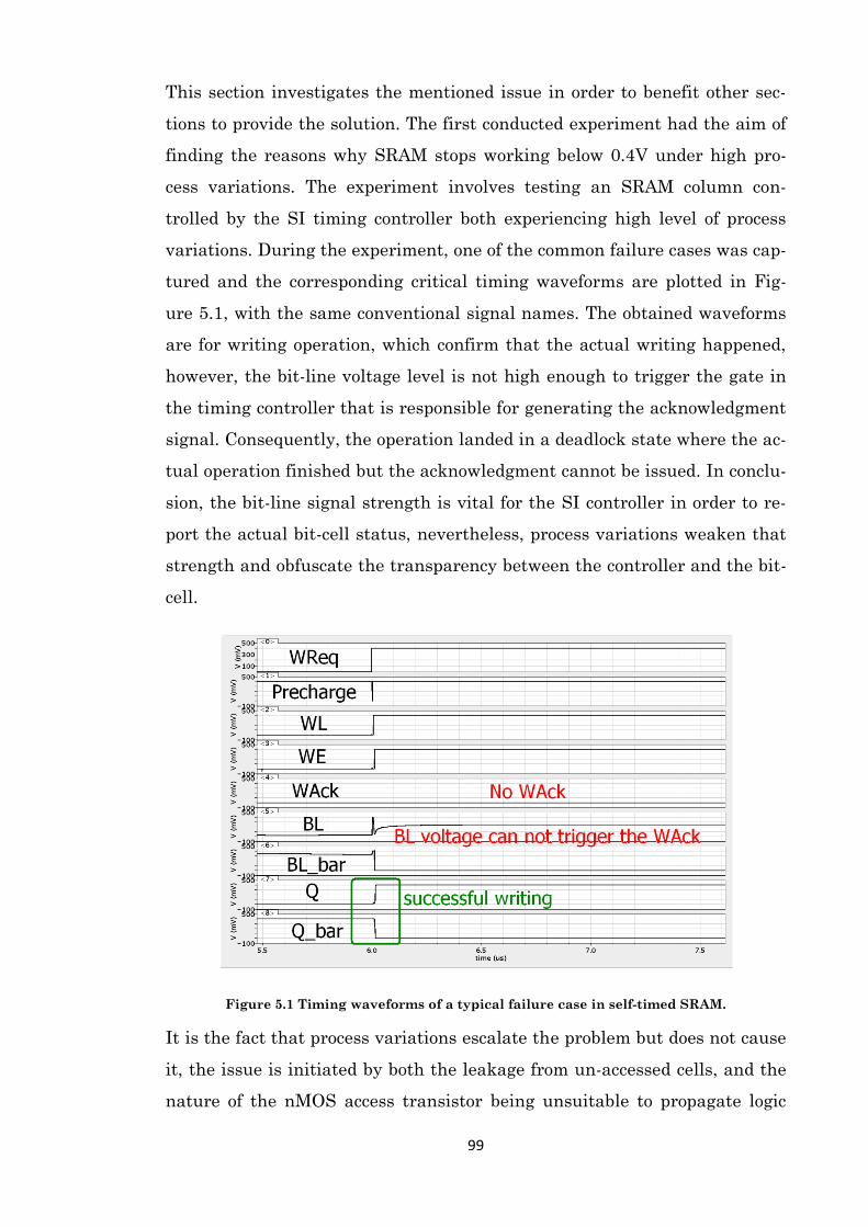
99
This section investigates the mentioned issue in order to benefit other sec-
tions to provide the solution. The first conducted experiment had the aim of
finding the reasons why SRAM stops working below 0.4V under high pro-
cess variations. The experiment involves testing an SRAM column con-
trolled by the SI timing controller both experiencing high level of process
variations. During the experiment, one of the common failure cases was cap-
tured and the corresponding critical timing waveforms are plotted in Fig-
ure 5.1, with the same conventional signal names. The obtained waveforms
are for writing operation, which confirm that the actual writing happened,
however, the bit-line voltage level is not high enough to trigger the gate in
the timing controller that is responsible for generating the acknowledgment
signal. Consequently, the operation landed in a deadlock state where the ac-
tual operation finished but the acknowledgment cannot be issued. In conclu-
sion, the bit-line signal strength is vital for the SI controller in order to re-
port the actual bit-cell status, nevertheless, process variations weaken that
strength and obfuscate the transparency between the controller and the bit-
cell.
Figure 5.1 Timing waveforms of a typical failure case in self-timed SRAM.
It is the fact that process variations escalate the problem but does not cause
it, the issue is initiated by both the leakage from un-accessed cells, and the
nature of the nMOS access transistor being unsuitable to propagate logic
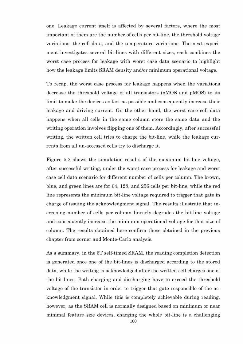
100
one. Leakage current itself is affected by several factors, where the most
important of them are the number of cells per bit-line, the threshold voltage
variations, the cell data, and the temperature variations. The next experi-
ment investigates several bit-lines with different sizes, each combines the
worst case process for leakage with worst case data scenario to highlight
how the leakage limits SRAM density and/or minimum operational voltage.
To recap, the worst case process for leakage happens when the variations
decrease the threshold voltage of all transistors (nMOS and pMOS) to its
limit to make the devices as fast as possible and consequently increase their
leakage and driving current. On the other hand, the worst case cell data
happens when all cells in the same column store the same data and the
writing operation involves flipping one of them. Accordingly, after successful
writing, the written cell tries to charge the bit-line, while the leakage cur-
rents from all un-accessed cells try to discharge it.
Figure 5.2 shows the simulation results of the maximum bit-line voltage,
after successful writing, under the worst case process for leakage and worst
case cell data scenario for different number of cells per column. The brown,
blue, and green lines are for 64, 128, and 256 cells per bit-line, while the red
line represents the minimum bit-line voltage required to trigger that gate in
charge of issuing the acknowledgment signal. The results illustrate that in-
creasing number of cells per column linearly degrades the bit-line voltage
and consequently increase the minimum operational voltage for that size of
column. The results obtained here confirm those obtained in the previous
chapter from corner and Monte-Carlo analysis.
As a summary, in the 6T self-timed SRAM, the reading completion detection
is generated once one of the bit-lines is discharged according to the stored
data, while the writing is acknowledged after the written cell charges one of
the bit-lines. Both charging and discharging have to exceed the threshold
voltage of the transistor in order to trigger that gate responsible of the ac-
knowledgment signal. While this is completely achievable during reading,
however, as the SRAM cell is normally designed based on minimum or near
minimal feature size devices, charging the whole bit-line is a challenging
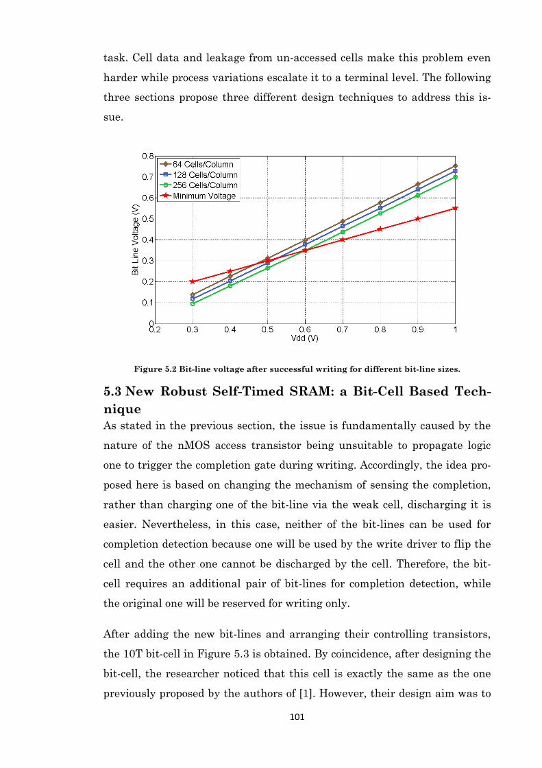
101
task. Cell data and leakage from un-accessed cells make this problem even
harder while process variations escalate it to a terminal level. The following
three sections propose three different design techniques to address this is-
sue.
Figure 5.2 Bit-line voltage after successful writing for different bit-line sizes.
5.3 New Robust Self-Timed SRAM: a Bit-Cell Based Tech-
nique
As stated in the previous section, the issue is fundamentally caused by the
nature of the nMOS access transistor being unsuitable to propagate logic
one to trigger the completion gate during writing. Accordingly, the idea pro-
posed here is based on changing the mechanism of sensing the completion,
rather than charging one of the bit-line via the weak cell, discharging it is
easier. Nevertheless, in this case, neither of the bit-lines can be used for
completion detection because one will be used by the write driver to flip the
cell and the other one cannot be discharged by the cell. Therefore, the bit-
cell requires an additional pair of bit-lines for completion detection, while
the original one will be reserved for writing only.
After adding the new bit-lines and arranging their controlling transistors,
the 10T bit-cell in Figure 5.3 is obtained. By coincidence, after designing the
bit-cell, the researcher noticed that this cell is exactly the same as the one
previously proposed by the authors of [1]. However, their design aim was to
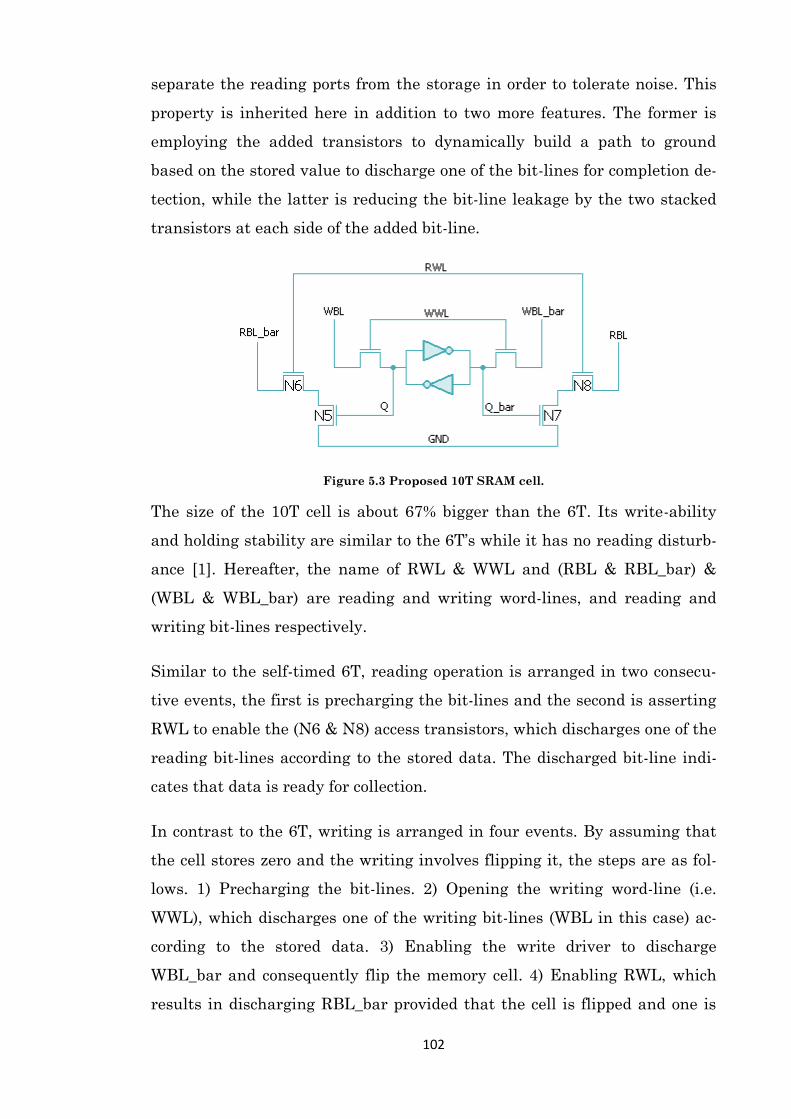
102
separate the reading ports from the storage in order to tolerate noise. This
property is inherited here in addition to two more features. The former is
employing the added transistors to dynamically build a path to ground
based on the stored value to discharge one of the bit-lines for completion de-
tection, while the latter is reducing the bit-line leakage by the two stacked
transistors at each side of the added bit-line.
Figure 5.3 Proposed 10T SRAM cell.
The size of the 10T cell is about 67% bigger than the 6T. Its write-ability
and holding stability are similar to the 6T’s while it has no reading disturb-
ance [1]. Hereafter, the name of RWL & WWL and (RBL & RBL_bar) &
(WBL & WBL_bar) are reading and writing word-lines, and reading and
writing bit-lines respectively.
Similar to the self-timed 6T, reading operation is arranged in two consecu-
tive events, the first is precharging the bit-lines and the second is asserting
RWL to enable the (N6 & N8) access transistors, which discharges one of the
reading bit-lines according to the stored data. The discharged bit-line indi-
cates that data is ready for collection.
In contrast to the 6T, writing is arranged in four events. By assuming that
the cell stores zero and the writing involves flipping it, the steps are as fol-
lows. 1) Precharging the bit-lines. 2) Opening the writing word-line (i.e.
WWL), which discharges one of the writing bit-lines (WBL in this case) ac-
cording to the stored data. 3) Enabling the write driver to discharge
WBL_bar and consequently flip the memory cell. 4) Enabling RWL, which
results in discharging RBL_bar provided that the cell is flipped and one is
103
generated from the other side to open the transistor N5, hence guaranteeing
the completion of writing operations.
As before, the STG specifications of the aforementioned events are in Fig-
ure 5.4, for writing and reading.
Figure 5.4 STG specifications for writing and reading in self-timed 10T SRAM.
Delay-Insensitive (DI) solution is the safest asynchronous logic as they work
correctly regardless of how much delay both wires and gates have [2]. How-
ever, DI is hard to implement or even impossible in some cases and the next
best option is the Quasi-Delay-Insensitive (QDI) or Speed Independent (SI)
circuits [3]. Figure 5.5 shows an SI solution mapped from the combined STG
specifications above. The circuit is designed by Petrify [4] and optimized
manually.
Figure 5.6 shows the waveforms obtained from the controller for reading (a)
and writing (b). The numbers 1 to 4 in the timing diagram are associated
with the reading and writing steps mentioned above.
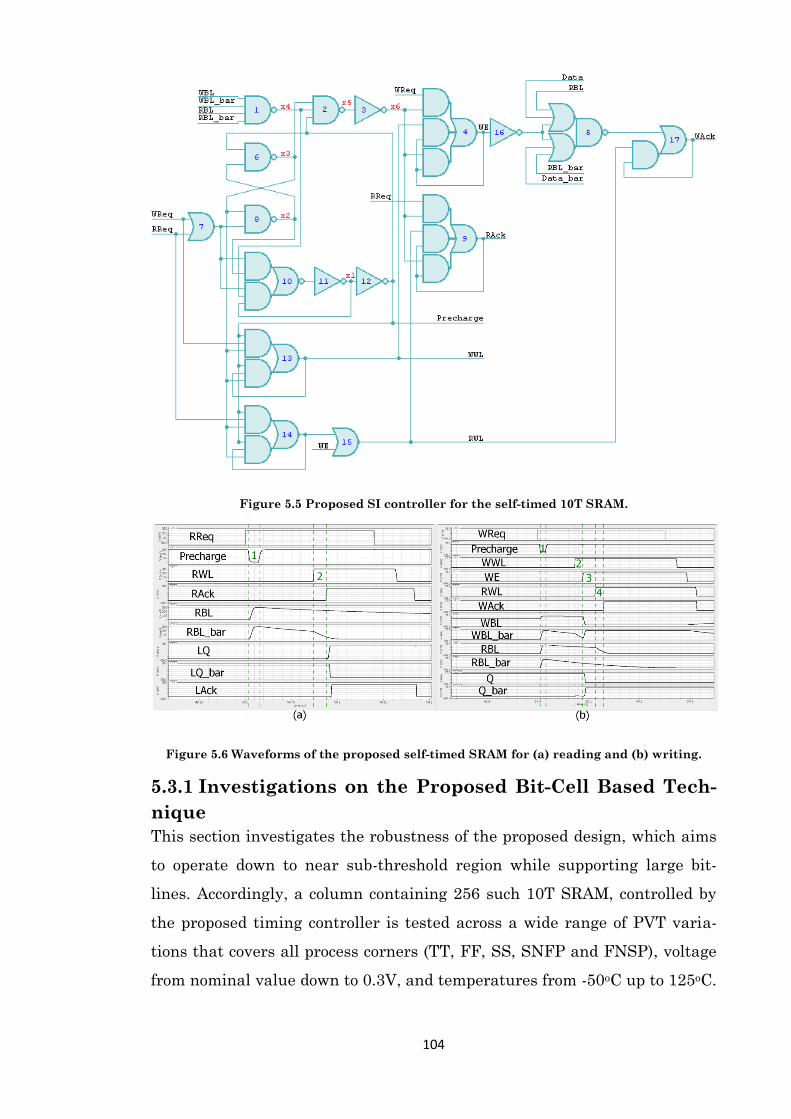
104
Figure 5.5 Proposed SI controller for the self-timed 10T SRAM.
Figure 5.6 Waveforms of the proposed self-timed SRAM for (a) reading and (b) writing.
5.3.1 Investigations on the Proposed Bit-Cell Based Tech-
nique
This section investigates the robustness of the proposed design, which aims
to operate down to near sub-threshold region while supporting large bit-
lines. Accordingly, a column containing 256 such 10T SRAM, controlled by
the proposed timing controller is tested across a wide range of PVT varia-
tions that covers all process corners (TT, FF, SS, SNFP and FNSP), voltage
from nominal value down to 0.3V, and temperatures from -50oC up to 125oC.
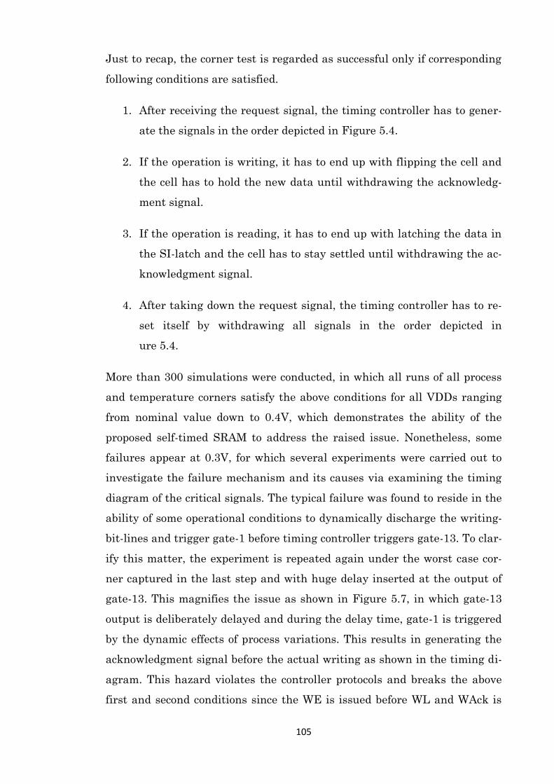
105
Just to recap, the corner test is regarded as successful only if corresponding
following conditions are satisfied.
1. After receiving the request signal, the timing controller has to gener-
ate the signals in the order depicted in Figure 5.4.
2. If the operation is writing, it has to end up with flipping the cell and
the cell has to hold the new data until withdrawing the acknowledg-
ment signal.
3. If the operation is reading, it has to end up with latching the data in
the SI-latch and the cell has to stay settled until withdrawing the ac-
knowledgment signal.
4. After taking down the request signal, the timing controller has to re-
set itself by withdrawing all signals in the order depicted in
ure 5.4.
More than 300 simulations were conducted, in which all runs of all process
and temperature corners satisfy the above conditions for all VDDs ranging
from nominal value down to 0.4V, which demonstrates the ability of the
proposed self-timed SRAM to address the raised issue. Nonetheless, some
failures appear at 0.3V, for which several experiments were carried out to
investigate the failure mechanism and its causes via examining the timing
diagram of the critical signals. The typical failure was found to reside in the
ability of some operational conditions to dynamically discharge the writing-
bit-lines and trigger gate-1 before timing controller triggers gate-13. To clar-
ify this matter, the experiment is repeated again under the worst case cor-
ner captured in the last step and with huge delay inserted at the output of
gate-13. This magnifies the issue as shown in Figure 5.7, in which gate-13
output is deliberately delayed and during the delay time, gate-1 is triggered
by the dynamic effects of process variations. This results in generating the
acknowledgment signal before the actual writing as shown in the timing di-
agram. This hazard violates the controller protocols and breaks the above
first and second conditions since the WE is issued before WL and WAck is
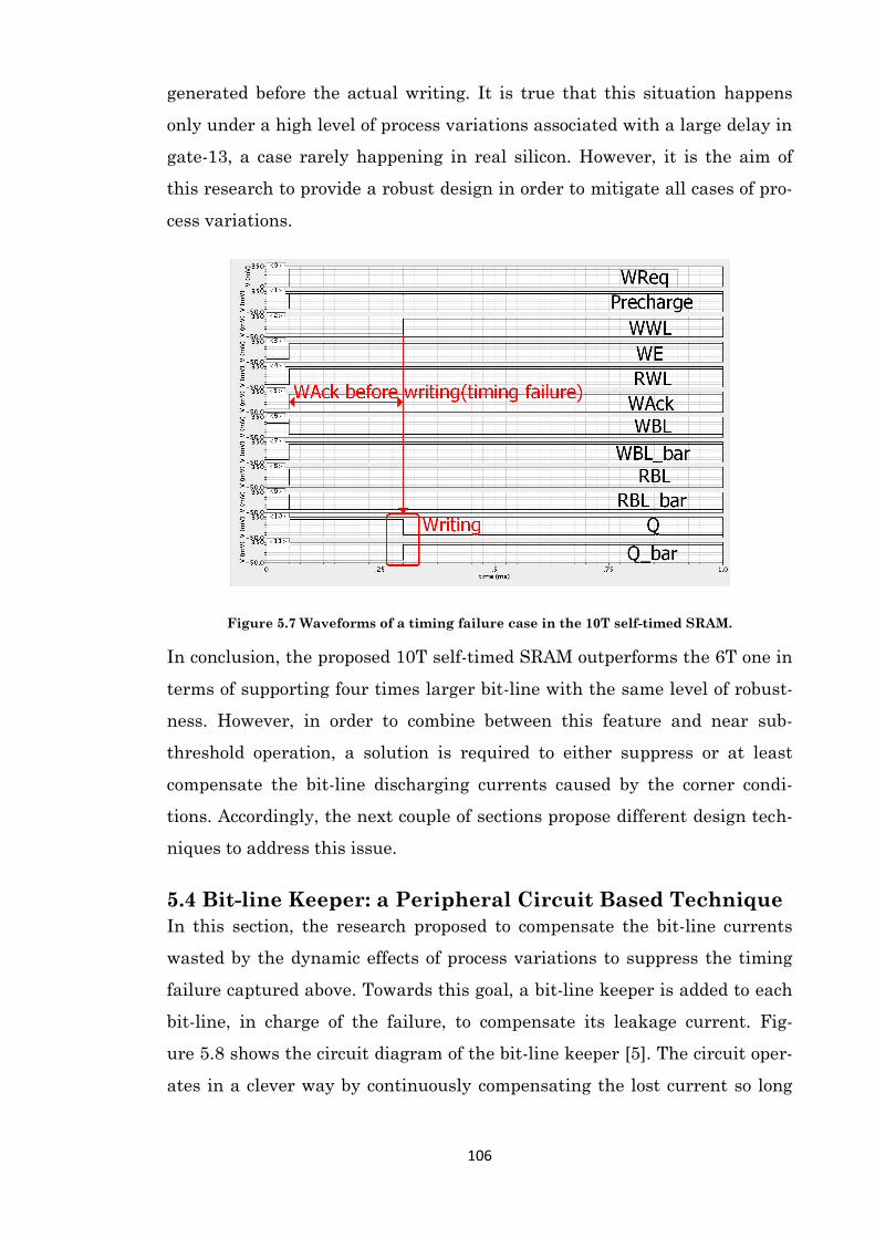
106
generated before the actual writing. It is true that this situation happens
only under a high level of process variations associated with a large delay in
gate-13, a case rarely happening in real silicon. However, it is the aim of
this research to provide a robust design in order to mitigate all cases of pro-
cess variations.
Figure 5.7 Waveforms of a timing failure case in the 10T self-timed SRAM.
In conclusion, the proposed 10T self-timed SRAM outperforms the 6T one in
terms of supporting four times larger bit-line with the same level of robust-
ness. However, in order to combine between this feature and near sub-
threshold operation, a solution is required to either suppress or at least
compensate the bit-line discharging currents caused by the corner condi-
tions. Accordingly, the next couple of sections propose different design tech-
niques to address this issue.
5.4 Bit-line Keeper: a Peripheral Circuit Based Technique
In this section, the research proposed to compensate the bit-line currents
wasted by the dynamic effects of process variations to suppress the timing
failure captured above. Towards this goal, a bit-line keeper is added to each
bit-line, in charge of the failure, to compensate its leakage current. Fig-
ure 5.8 shows the circuit diagram of the bit-line keeper [5]. The circuit oper-
ates in a clever way by continuously compensating the lost current so long
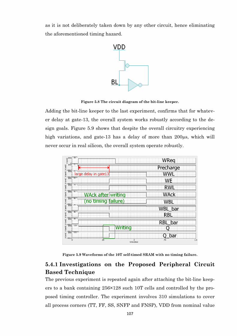
107
as it is not deliberately taken down by any other circuit, hence eliminating
the aforementioned timing hazard.
Figure 5.8 The circuit diagram of the bit-line keeper.
Adding the bit-line keeper to the last experiment, confirms that for whatev-
er delay at gate-13, the overall system works robustly according to the de-
sign goals. Figure 5.9 shows that despite the overall circuitry experiencing
high variations, and gate-13 has a delay of more than 200µs, which will
never occur in real silicon, the overall system operate robustly.
Figure 5.9 Waveforms of the 10T self-timed SRAM with no timing failure.
5.4.1 Investigations on the Proposed Peripheral Circuit
Based Technique
The previous experiment is repeated again after attaching the bit-line keep-
ers to a bank containing 256×128 such 10T cells and controlled by the pro-
posed timing controller. The experiment involves 310 simulations to cover
all process corners (TT, FF, SS, SNFP and FNSP), VDD from nominal value
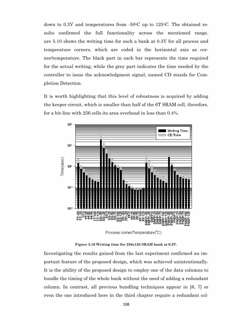
108
down to 0.3V and temperatures from -50oC up to 125oC. The obtained re-
sults confirmed the full functionality across the mentioned range.
ure 5.10 shows the writing time for such a bank at 0.3V for all process and
temperature corners, which are coded in the horizontal axis as cor-
ner/temperature. The black part in each bar represents the time required
for the actual writing, while the grey part indicates the time needed by the
controller to issue the acknowledgment signal, named CD stands for Com-
pletion Detection.
It is worth highlighting that this level of robustness is acquired by adding
the keeper circuit, which is smaller than half of the 6T SRAM cell, therefore,
for a bit-line with 256 cells its area overhead in less than 0.4%.
Figure 5.10 Writing time for 256x128 SRAM bank at 0.3V.
Investigating the results gained from the last experiment confirmed an im-
portant feature of the proposed design, which was achieved unintentionally.
It is the ability of the proposed design to employ one of the data columns to
bundle the timing of the whole bank without the need of adding a redundant
column. In contrast, all previous bundling techniques appear in [6, 7] or
even the one introduced here in the third chapter require a redundant col-
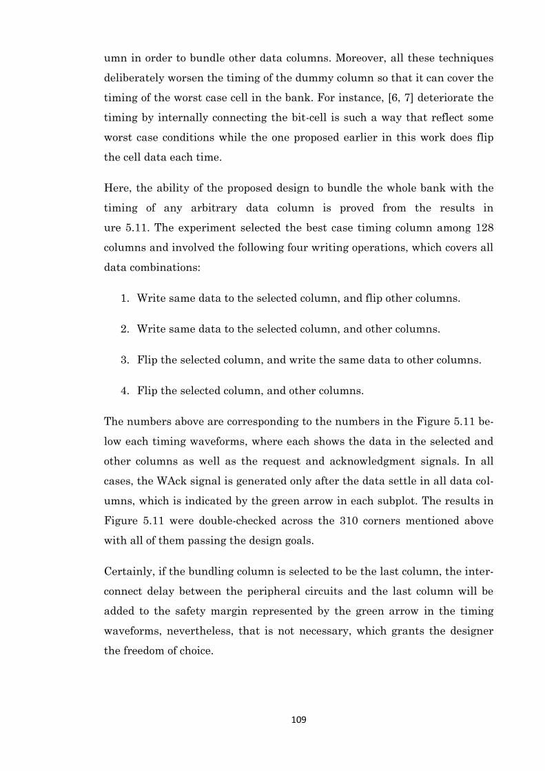
109
umn in order to bundle other data columns. Moreover, all these techniques
deliberately worsen the timing of the dummy column so that it can cover the
timing of the worst case cell in the bank. For instance, [6, 7] deteriorate the
timing by internally connecting the bit-cell is such a way that reflect some
worst case conditions while the one proposed earlier in this work does flip
the cell data each time.
Here, the ability of the proposed design to bundle the whole bank with the
timing of any arbitrary data column is proved from the results in
ure 5.11. The experiment selected the best case timing column among 128
columns and involved the following four writing operations, which covers all
data combinations:
1. Write same data to the selected column, and flip other columns.
2. Write same data to the selected column, and other columns.
3. Flip the selected column, and write the same data to other columns.
4. Flip the selected column, and other columns.
The numbers above are corresponding to the numbers in the Figure 5.11 be-
low each timing waveforms, where each shows the data in the selected and
other columns as well as the request and acknowledgment signals. In all
cases, the WAck signal is generated only after the data settle in all data col-
umns, which is indicated by the green arrow in each subplot. The results in
Figure 5.11 were double-checked across the 310 corners mentioned above
with all of them passing the design goals.
Certainly, if the bundling column is selected to be the last column, the inter-
connect delay between the peripheral circuits and the last column will be
added to the safety margin represented by the green arrow in the timing
waveforms, nevertheless, that is not necessary, which grants the designer
the freedom of choice.
110
1 2
3 4
Figure 5.11 Timing diagram of writing operation that shows the data in the bundling and
bundled columns.
In conclusion, adding the bit-line keepers to the proposed 10T self-timed
SRAM gives it the opportunity to work robustly near the sub-threshold re-
gion while supporting large bit-lines. As an unprecedented achievement,
which has not yet been reported either in synchronous or asynchronous
SRAM, the proposed design is able to employ one of the data columns as a
bundling column, which was proven across a wide range of PVT variations.
This achievement improves the SRAM area density as well.
5.5 Virtual Ground: a Voltage Level Based Technique
By the end of section 5.3, this research acquired a new self-timed SRAM
based on the 10T bit-cell, which is able to work robustly down to 0.4V across
a wide range of PT variations. In that section, it is found that, there is a
timing hazard happening below 0.4V at some corners, which is then ad-
dressed at section 5.4 by introducing the bit-line keeper. Moreover, keeper is
categorized as a peripheral circuit based technique, which compensates the
bit-line leakage currents.
111
This section aims to propose a new design that improves the energy efficien-
cy of the 10T self-timed SRAM with keepers. This opportunity clearly ap-
pears after careful inspection of the last design, in which three events were
found to waste useless amounts of energy as follows.
1. All bit-lines are precharged, however, only reading ones suffice for
monitoring the bit-cell. Hence, it is suggested to precharge the read-
ing bit-lines only to save the wasted energy from two aspects, preserv-
ing the charging currents and decreasing the precharging time.
2. Keepers compensate the wasted bit-line current by wasting more,
where a better solution is to suppress the wastage rather than com-
pensate for it. Accordingly, it is recommended to suppress the leakage
current by means of a virtual ground, a well known design technique
introduced before for synchronous SRAM [8, 9].
3. Writing-word-line is enabled before the write driver for no purpose. If,
however, they are swapped, both the driving current of the access
transistors and the time during which they are enabled will be de-
creased and that saves energy.
Unfortunately, the first and last recommendations require updating some
gates in the timing controller to consider the new signal sequences while the
second suggestion requires introducing a new signal to control the virtual
ground of all cells in the same row. Firstly, the 10T bit-cell needs the update
shown in Figure 5.12. VGNDC is the virtual ground control signal, when it
is low, the reading bit-lines have no path to the ground and therefore it
maintains its current, however, when it is high, the discharging path is re-
covered and the cell works as usual. According to the suggested signals se-
quence, including the added one for virtual ground, the new STG specifica-
tions are shown in Figure 5.13 for reading and writing.
In this STG, one more event is added to the reading operation, exactly after
precharging the reading-bit-lines and before opening the reading-word-line,
which is to assert the VGNDC signal to recover the discharging path of the
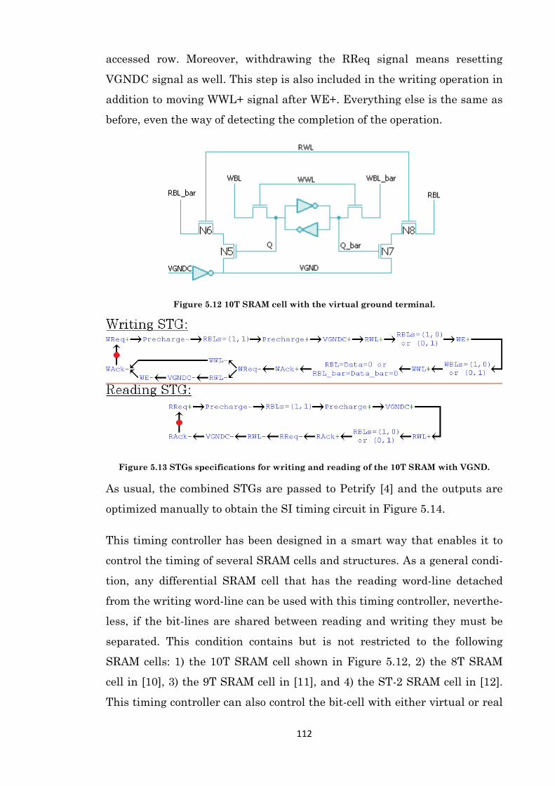
112
accessed row. Moreover, withdrawing the RReq signal means resetting
VGNDC signal as well. This step is also included in the writing operation in
addition to moving WWL+ signal after WE+. Everything else is the same as
before, even the way of detecting the completion of the operation.
Figure 5.12 10T SRAM cell with the virtual ground terminal.
Figure 5.13 STGs specifications for writing and reading of the 10T SRAM with VGND.
As usual, the combined STGs are passed to Petrify [4] and the outputs are
optimized manually to obtain the SI timing circuit in Figure 5.14.
This timing controller has been designed in a smart way that enables it to
control the timing of several SRAM cells and structures. As a general condi-
tion, any differential SRAM cell that has the reading word-line detached
from the writing word-line can be used with this timing controller, neverthe-
less, if the bit-lines are shared between reading and writing they must be
separated. This condition contains but is not restricted to the following
SRAM cells: 1) the 10T SRAM cell shown in Figure 5.12, 2) the 8T SRAM
cell in [10], 3) the 9T SRAM cell in [11], and 4) the ST-2 SRAM cell in [12].
This timing controller can also control the bit-cell with either virtual or real
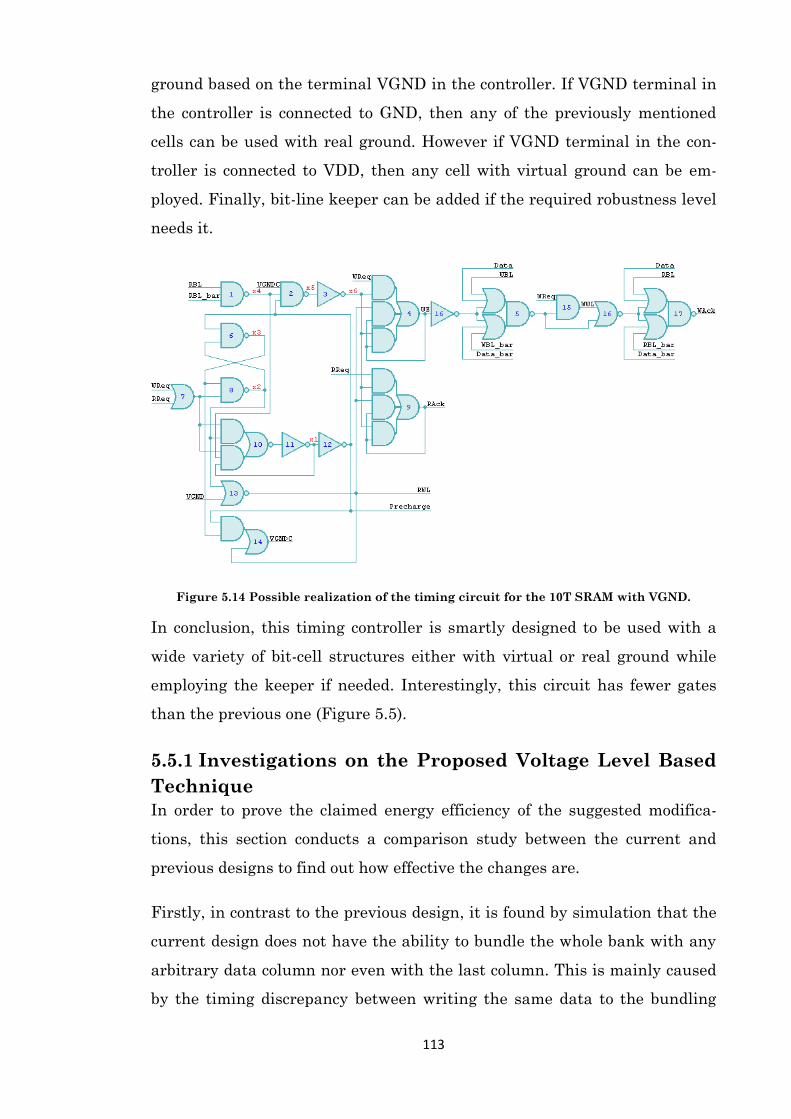
113
ground based on the terminal VGND in the controller. If VGND terminal in
the controller is connected to GND, then any of the previously mentioned
cells can be used with real ground. However if VGND terminal in the con-
troller is connected to VDD, then any cell with virtual ground can be em-
ployed. Finally, bit-line keeper can be added if the required robustness level
needs it.
Figure 5.14 Possible realization of the timing circuit for the 10T SRAM with VGND.
In conclusion, this timing controller is smartly designed to be used with a
wide variety of bit-cell structures either with virtual or real ground while
employing the keeper if needed. Interestingly, this circuit has fewer gates
than the previous one (Figure 5.5).
5.5.1 Investigations on the Proposed Voltage Level Based
Technique
In order to prove the claimed energy efficiency of the suggested modifica-
tions, this section conducts a comparison study between the current and
previous designs to find out how effective the changes are.
Firstly, in contrast to the previous design, it is found by simulation that the
current design does not have the ability to bundle the whole bank with any
arbitrary data column nor even with the last column. This is mainly caused
by the timing discrepancy between writing the same data to the bundling
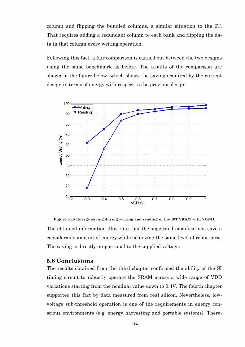
114
column and flipping the bundled columns, a similar situation to the 6T.
That requires adding a redundant column to each bank and flipping the da-
ta in that column every writing operation.
Following this fact, a fair comparison is carried out between the two designs
using the same benchmark as before. The results of the comparison are
shown in the figure below, which shows the saving acquired by the current
design in terms of energy with respect to the previous design.
Figure 5.15 Energy saving during writing and reading in the 10T SRAM with VGND.
The obtained information illustrate that the suggested modifications save a
considerable amount of energy while achieving the same level of robustness.
The saving is directly proportional to the supplied voltage.
5.6 Conclusions
The results obtained from the third chapter confirmed the ability of the SI
timing circuit to robustly operate the SRAM across a wide range of VDD
variations starting from the nominal value down to 0.4V. The fourth chapter
supported this fact by data measured from real silicon. Nevertheless, low-
voltage sub-threshold operation is one of the requirements in energy con-
scious environments (e.g. energy harvesting and portable systems). There-
115
fore, it is the aim of this research to operate the SRAM robustly down to the
sub-threshold region, or at least near it, while supporting large bit-lines.
Hence, this chapter is dedicated for that goal.
The work in this chapter was started by preliminary analysis to investigate
the failure issue near the sub-threshold region and that was found to be the
inability of the controller to generate the acknowledgment signal after suc-
cessful writing due to two main reasons. The former is the dependency upon
the nMOS access transistors to propagate logic one while the latter is the
leakage from un-accessed cells. The latter increases as the bit-line length
increases and hence it limits the area density of the SRAM. Following that
investigation, the chapter explored some SRAM design techniques to ad-
dress the mentioned issue.
According to the categorization of the SRAM design techniques described in
the second chapter, the first solution is a bit-cell based technique, which in-
volved proposing a new 10T bit-cell to address the aforementioned matter.
The new cell features a new method of detecting the completion via charging
the bit-line instead of discharging it and employing stacked transistors to
decrease the leakage from un-accessed cells. Based upon the simulation da-
ta, the solution is able to support large bit-lines while operating robustly
down to 0.4V. However, near sub-threshold operation failed due to timing
hazard in the controller protocols caused by the dynamic effects of the pro-
cess variations.
Then the study introduced the bit-line keeper, which is a peripheral circuit
based technique, in order to compensate for the leakage currents, which
cause the timing hazard. Adding that component to the design enabled it to
reach the design goal by supporting large bit-lines and working robustly
down to near sub-threshold region.
The careful inspections of the last design suggested several modifications to
increase the energy efficiency of the whole design. The main recommenda-
tion is suppressing the leakage by the means of virtual ground technique
instead of compensating it with the keeper. Accordingly, the bit-cell and its
116
timing controller are updated to accommodate the suggestions. The new
timing circuitry is smartly designed to allow it to be used with a wide varie-
ty of bit-cell structures, four of them were listed above, with either virtual or
real ground. The obtained results confirm saving considerable amount of
energy for the same level of robustness.
5.7 References 1. H. Noguchi et al., "Which is the Best Dual-Port SRAM in 45-nm Process Technology? - 8T, 10T
Single End, and 10T Differential -" in Integrated Circuit Design and Technology and Tutorial, 2008.
ICICDT 2008. IEEE International Conference on, 2008, pp. 55-58.
2. S. Jens and S. Furber, Principles of Asynchronous Circuit Design: A Systems Perspective: Springer,
2001.
3. J. M. Alain, "The Limitations to Delay-Insensitivity in Asynchronous Circuits," presented at the Pro-
ceedings of the sixth MIT conference on Advanced research in VLSI, Boston, Massachusetts, USA,
1990.
4. J. Cortadella et al., "Petrify: A Tool for Manipulating Concurrent Specifications and Synthesis of
Asynchronous Controllers," IEICE TRANSACTIONS on Information and Systems, vol. E80-D, pp. 315-
325, 1997.
5. R. K. Krishnamurthy et al., "A 130-nm 6-GHz 256 × 32 Bit Leakage-Tolerant Register File," Solid-
State Circuits, IEEE Journal of, vol. 37, pp. 624-632, 2002.
6. C. Meng-Fan, Y. Sue-Meng, and C. Kung-Ting, "Wide VDD Embedded Asynchronous SRAM with
Dual-Mode Self-Timed Technique for Dynamic Voltage Systems," Circuits and Systems I: Regular
Papers, IEEE Transactions on, vol. 56, pp. 1657-1667, 2009.
7. B. S. Amrutur and M. A. Horowitz, "A Replica Technique for Wordline and Sense Control in Low-
Power SRAM's," Solid-State Circuits, IEEE Journal of, vol. 33, pp. 1208-1219, 1998.
8. N. Verma and A. P. Chandrakasan, "A 256 kb 65 nm 8T Subthreshold SRAM Employing Sense-
Amplifier Redundancy," Solid-State Circuits, IEEE Journal of, vol. 43, pp. 141-149, 2008.
9. C. Ik Joon et al., "A 32 kb 10T Sub-Threshold SRAM Array with Bit-Interleaving and Differential
Read Scheme in 90 nm CMOS," Solid-State Circuits, IEEE Journal of, vol. 44, pp. 650-658, 2009.
10. J. P. Kulkarni et al., "A Read-Disturb-Free, Differential Sensing 1R/1W Port, 8T Bitcell Array," Very
Large Scale Integration (VLSI) Systems, IEEE Transactions on, vol. 19, pp. 1727-1730, 2011.
11. L. Zhiyu and V. Kursun, "Characterization of a Novel Nine-Transistor SRAM Cell," Very Large Scale
Integration (VLSI) Systems, IEEE Transactions on, vol. 16, pp. 488-492, 2008.
12. J. P. Kulkarni et al., "Process Variation Tolerant SRAM Array for Ultra Low Voltage Applications," in
Design Automation Conference, 2008. DAC 2008. 45th ACM/IEEE, 2008, pp. 108-113.
13. S. G. Narendra and A. P. Chandrakasan, Leakage in Nanometer CMOS Technologies: Springer, 2006.
117
Chapter 6. Conclusions and Future Work
6.1 Introduction
This chapter ends the thesis by concluding the whole project and proposing
promising follow-on research studies. Therefore, the current chapter is di-
vided into two main sections, the first is the conclusions, and the second is
the future work.
6.2 View and Review
The story of the current technologies began after Jack Kilby introduced the
IC in 1958 [1], and M. M. (John) Atalla and Dawon Kahng invented the Sili-
con MOSFET transistor in 1959 [2]. Certainly, this story has many other
unsung heroes, however, the mentioned are the most important milestones
of the technology journey [3].
Since then and the industry has been driven towards increasing the perfor-
mance and functionality of the computational logic while decreasing its
manufacturing cost and power consumption, which is achieved via downsiz-
ing the dimensions of the components embedded in the ICs. This clearly ap-
pears when comparing early ICs, which had a line width of 25.4 µm with
that one in 1972 with a gate length of 6.0 µm [4, 5]. At that time, most of the
research were directed towards the scaling process, as a promising field. For
instance, in 1974, a scaling method was proposed in [6], which assumed that
all the device parameters are either shrunk or increased by the same factor
(e.g. K). More precisely, the technique involves scaling all device dimen-
sions, threshold voltage, supply voltage, and drain current by 1/K. Conse-
quently, the gate area and charge will be reduced by 1/K2, and circuit per-
formance will be increased by K. Moreover, if the chip size is kept fixed, the
118
number of transistors per die will be increase by K2 every generation. If all
these conditions are satisfied, the result will be increasing the functionality
and performance of the IC every generation while keeping the power con-
sumption constant, accordingly, this scaling is called ideal scaling [5, 7].
Nevertheless, the actual scaling has been more aggressive than the ideal
one, due to the fact that the goals of the latter lag substantially behind the
dream of the industry. That aggressive scaling scales key parameters of the
device independently and the results are significant increase in the perfor-
mance of the die and the number of transistors it has with marginal de-
crease in the supply voltage and threshold voltage. Accordingly, the die
power consumption increased by several orders of magnitude, more specifi-
cally, it roughly doubled every two years [5, 8]. This considerable growth in
power consumption makes it one of the main design concerns for both porta-
ble and non-portable systems. In the case of battery alone powered systems,
the problem is even worse as the increase in power cannot be accommodated
by the improvement in the battery capacity, which only doubles every ten
years [8]. In addition to the limitations in battery capacity, in many cases,
maintaining and replacing batteries are impossible, inconvenient, costly, or
hazardous. This suggests developing a new generation of microelectronic
systems that can be self-powered, the opportunity of which was made clear
by the advances in both the field of micro-generators, and low power elec-
tronics. In the scope of that, this research study attempted to propose a
proof of concept for enabling energy harvesting microelectronics via intro-
ducing several design methods for this area. The investigations conducted
by this study concentrate on SRAM, as it occupies the majority of the chip
area and affects most of its performance parameters, moreover, it is a vital
component for all computational logic.
The first experiment in this research analysed the behaviour of the SRAM
under variable VDD, a typical case in energy harvesting systems. The ex-
periment confirmed the unsuitability of the simple chain of basic gates to
bundle the SRAM timing in a highly variable supply voltage environment,
otherwise, the wastage of resources might reach up to three times of the re-
119
quired amount. Accordingly, this research proposed to regulate the data
flow inside the SRAM system based on the actual speed of the circuit via
employing handshaking protocols and eliminate all timing assumptions.
Nevertheless, the literature affirms that SRAM has not yet benefited from
completion detection, especially for writing, due to an erroneous speculation
that writing acknowledgment is difficult or even impossible to implement in
SRAM. Thereafter, the study carried on by proposing a dynamic technique
to detect the completion of both reading and writing in SRAM. Moreover,
the obtained behavioural specifications were successfully synthesized in a
fully SI circuit realisation for the aim of robust operation. The designed cir-
cuitry was employed in an SRAM system, where the whole design was
proved, by simulation, to have the ability of working under highly variable
VDD. Furthermore, the timing signals issued by the circuitry reports all ac-
tivities inside the bit-cell, not only the completion of the whole operation but
further the completion of each stage the main operation has. Interestingly,
the task of monitoring the cell is achieved via a basic NAND gate. In con-
trast to conventional SRAM, the proposed one is able to function while the
system changes the operational mode (DVS) with no need to stop working or
waiting the supply voltage to settle down. In contrast to synchronous
SRAM, the timing circuit proposed here has the ability to control both the
performance and energy of the SRAM via only one knob, the VDD. Based on
that design, another design was proposed which is faster but less safe as it
depends upon bundling the whole SRAM with the handshaking signals from
last column. Despite that, the bundling technique is still safer than those in
the literature since it reflects real operation in real cells while other tech-
niques reflect worst case timing in dummy cells.
Following this step, it was the time to prove the actual functionality in real
silicon. Hence, the proposed design was combined with some other testing
circuitry to test the whole design in an asynchronous and autonomous man-
ner. The whole design showed full functionality down to above the sub-
threshold region under high process variations, which encouraged taping
out the chip. Nevertheless, the testing goals landed the chip in a situation
requiring dual supply voltage along with a proper signal communication
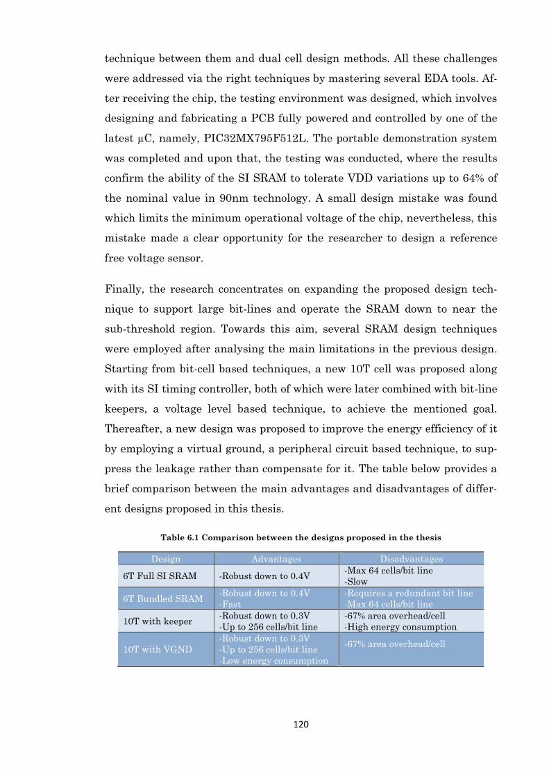
120
technique between them and dual cell design methods. All these challenges
were addressed via the right techniques by mastering several EDA tools. Af-
ter receiving the chip, the testing environment was designed, which involves
designing and fabricating a PCB fully powered and controlled by one of the
latest µC, namely, PIC32MX795F512L. The portable demonstration system
was completed and upon that, the testing was conducted, where the results
confirm the ability of the SI SRAM to tolerate VDD variations up to 64% of
the nominal value in 90nm technology. A small design mistake was found
which limits the minimum operational voltage of the chip, nevertheless, this
mistake made a clear opportunity for the researcher to design a reference
free voltage sensor.
Finally, the research concentrates on expanding the proposed design tech-
nique to support large bit-lines and operate the SRAM down to near the
sub-threshold region. Towards this aim, several SRAM design techniques
were employed after analysing the main limitations in the previous design.
Starting from bit-cell based techniques, a new 10T cell was proposed along
with its SI timing controller, both of which were later combined with bit-line
keepers, a voltage level based technique, to achieve the mentioned goal.
Thereafter, a new design was proposed to improve the energy efficiency of it
by employing a virtual ground, a peripheral circuit based technique, to sup-
press the leakage rather than compensate for it. The table below provides a
brief comparison between the main advantages and disadvantages of differ-
ent designs proposed in this thesis.
Table 6.1 Comparison between the designs proposed in the thesis
Design Advantages Disadvantages
6T Full SI SRAM -Robust down to 0.4V -Max 64 cells/bit line
-Slow
6T Bundled SRAM -Robust down to 0.4V
-Fast
-Requires a redundant bit line
-Max 64 cells/bit line
10T with keeper -Robust down to 0.3V
-Up to 256 cells/bit line
-67% area overhead/cell
-High energy consumption
10T with VGND
-Robust down to 0.3V
-Up to 256 cells/bit line
-Low energy consumption
-67% area overhead/cell
121
6.3 Prospective Future Research
The investigations, analysis, and experiments conducted during this re-
search along with the obtained results from real silicon suggested several
promising proposals for the future research.
According to the ITRS reports, clock-less designs will be increased in future
SoC [9, 10], in which the majority of the area is occupied by the memory.
This highly probable prediction encourages designers to investigate self-
timed memory system in more details and optimize its operation to satisfy
most of the applications requirements.
Firstly and most importantly, reliability is a crucial metric for all memory
systems, especially in low power and energy harvesting systems, as lowering
the VDD badly deteriorates reliability. Process variations have different im-
pacts on different components of a memory subsystem. For instance, the
high leakage currents in submicron technologies are generally considered as
a main concern in terms of power consumption and more recently in terms
of fault modelling [11]. Mostly, variations affect the threshold voltage and
eventually the leakage and latency. Nonetheless, the proposed SI SRAM co-
vers the latency related faults as previously demonstrated.
In a highly reliable system, fault detection is vital. The earlier a fault is de-
tected, the better a system is. Conventionally, the faults are detected by a
series of writing and reading and/or some dedicated hardware. However, as
the proposed self-timed SRAM uses closed loop control, all operations are
controllable. For instance, previous chapters showed a writing fault, which
causes a deadlock eventually. The same problem can happen in reading. As
an example, during reading, after precharging, if the leakage current is
high, it will discharge the bit lines and eventually reading acknowledgment
is generated wrongly. These leakage faults can be detected either from dead-
locks or from wrong relationships in control signals.
Asynchronous handshaking protocols can be verified via different tech-
niques, for instance, in [12] a low cost method was proposed to check the
handshaking protocols during the run time of asynchronous circuits. Accord-
122
ing to the obtained results, the design is able to detect both deadlocks and
wrong relationships in the protocols.
Moreover, Data Retention Voltage (DRV) is an important parameter of a
highly reliable system for low power operations. For idle memory banks,
lowering the supply to the DRV level enables dramatic reduction of the
wastage energy. Nevertheless, the DRV depends on the extremes of local
mismatch variations, where design time decisions may need to be so con-
servative as to render this technique useless or at least less efficient.
Several and different DRV tracking techniques have been already proposed
and the most important of them were discussed previously. While each
method advances the state of the art in some aspects, it suffers from many
limitations. In conclusion, to the best of the researcher’s knowledge and un-
til the date of writing this chapter, there is no fully on-chip design that can
detect the actual DRV of the SRAM bank during the runtime and control
the voltage level accordingly without sacrificing the stored data.
On the other hand, with the self-timed memory, when the supply voltage is
reduced to a certain point, the controller stops working properly because of
the sensing mechanism embedded in the controller as discussed previously.
From the experiments in the previous chapters, it is clear that in that situa-
tion the data is still correct, but the sensing mechanism stops working. The
voltage that the memory stops working at is still higher than the DRV, how-
ever, it is very close to the minimum energy point.
Consequently, such self-timed SRAM can be regarded somehow as self-
sensing for usable DRV and an asynchronous deadlock or conflict detector
can then be employed to generate a warning signal to raise system voltage.
In summary, the future research might concentrate on designing a new
memory controller that is able to bind the DRV with some signals and gives
the user the opportunity to calibrate the safe margin between the actual
DRV and the generated DRV in order to cope with the error rate of the ap-
123
plication. Nevertheless, the controller must have the ability to determine
the actual DRV on-chip.
Other research projects might focus upon improving the area density of self-
timed memory via enhancing the strength of the completion signal, which
can be achieved by partitioning the bit-lines and adding some logic after
each partition in order to save the safe operation of the complete timing
path.
The future research should not overlook the clear opportunity of designing
reference free voltage sensors. The feasibility of this idea has already been
supported by data from real silicon and now it just requires more analysis
and investigation. According to the design and obtained results, such a sen-
sor is very cheap it terms of area and energy while it provides high accuracy
and similarity between the design time output and the silicon data.
Finally, it is certainly a good idea for upcoming research to benefit from the
robustness of self-timed memory system in the context of high performance
processors.
6.4 References 1. Texas Instruments, An Interview with Jack Kilby [online]. Available:
www.ti.com/corp/docs/kilbyctr/interview.shtml.
2. D. Kahng, “A Historical Perspective on the Development of MOS Transistors and Related Devices,”
Electron Devices, IEEE Transactions on, vol. 23, no. 7, pp. 655-657, 1976.
3. C.-T. Sah, "Evolution of the MOS Transistor-from Conception to VLSI," Proceedings of the IEEE, vol.
76, pp. 1280-1326, 1988.
4. G. E. Moore, "Progress in Digital Integrated Electronics," in Electron Devices Meeting, 1975 Interna-
tional, 1975, pp. 11-13.
5. H. Iwai, "CMOS Technology-Year 2010 and Beyond," Solid-State Circuits, IEEE Journal of, vol. 34,
pp. 357-366, 1999.
6. R. H. Dennard et al., "Design of Ion-Implanted MOSFET's with Very Small Physical Dimensions,"
Solid-State Circuits, IEEE Journal of, vol. 9, pp. 256-268, 1974.
7. H. Iwai, "Roadmap for 22 nm and Beyond (Invited Paper)," Microelectronic Engineering, vol. 86, pp.
1520-1528, 7// 2009.
8. J. M. Rabaey, Low Power Design Essentials: Springer London, Limited, 2009.
9. B. M. Al-Hashimi, System-on-Chip: Next Generation Electronics: The Institution of Engineering and
Technology, 2006.
10. The International Technology Roadmap for Semiconductors, ITRS Home [online]. Available:
http://www.itrs.net/.
11. S. G. Narendra and A. P. Chandrakasan, Leakage in Nanometer CMOS Technologies: Springer, 2006.
12. D. Shang et al., "Low-Cost Online Testing of Asynchronous Handshakes," in Test Symposium, 2006.
ETS '06. Eleventh IEEE European, 2006, pp. 225-232.
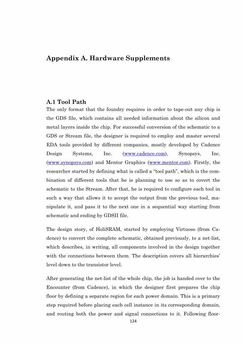
124
Appendix A. Hardware Supplements
A.1 Tool Path
The only format that the foundry requires in order to tape-out any chip is
the GDS file, which contains all needed information about the silicon and
metal layers inside the chip. For successful conversion of the schematic to a
GDS or Stream file, the designer is required to employ and master several
EDA tools provided by different companies, mostly developed by Cadence
Design Systems, Inc. (www.cadence.com), Synopsys, Inc.
(www.synopsys.com) and Mentor Graphics (www.mentor.com). Firstly, the
researcher started by defining what is called a “tool path”, which is the com-
bination of different tools that he is planning to use so as to covert the
schematic to the Stream. After that, he is required to configure each tool in
such a way that allows it to accept the output from the previous tool, ma-
nipulate it, and pass it to the next one in a sequential way starting from
schematic and ending by GDSII file.
The design story, of HoliSRAM, started by employing Virtuoso (from Ca-
dence) to convert the complete schematic, obtained previously, to a net-list,
which describes, in writing, all components involved in the design together
with the connections between them. The description covers all hierarchies’
level down to the transistor level.
After generating the net-list of the whole chip, the job is handed over to the
Encounter (from Cadence), in which the designer first prepares the chip
floor by defining a separate region for each power domain. This is a primary
step required before placing each cell instance in its corresponding domain,
and routing both the power and signal connections to it. Following floor-
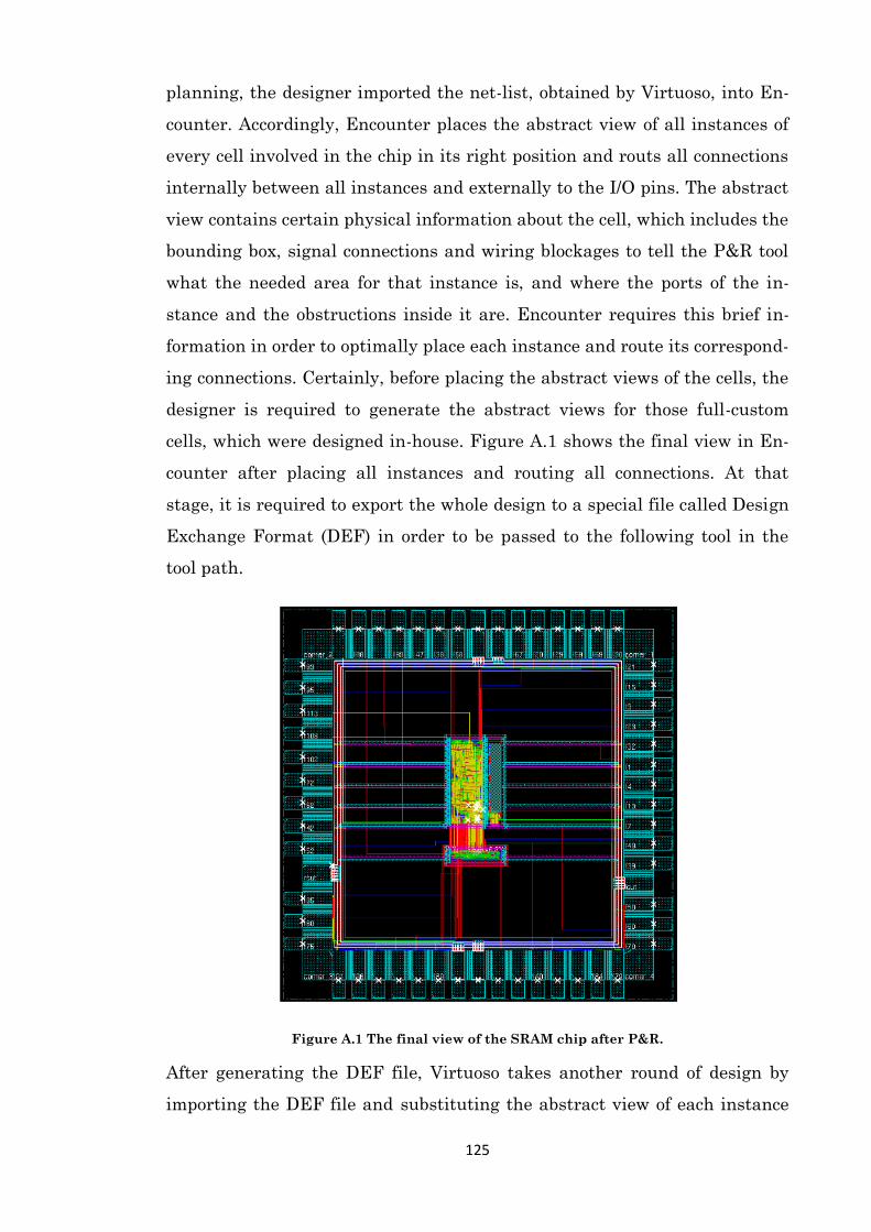
125
planning, the designer imported the net-list, obtained by Virtuoso, into En-
counter. Accordingly, Encounter places the abstract view of all instances of
every cell involved in the chip in its right position and routs all connections
internally between all instances and externally to the I/O pins. The abstract
view contains certain physical information about the cell, which includes the
bounding box, signal connections and wiring blockages to tell the P&R tool
what the needed area for that instance is, and where the ports of the in-
stance and the obstructions inside it are. Encounter requires this brief in-
formation in order to optimally place each instance and route its correspond-
ing connections. Certainly, before placing the abstract views of the cells, the
designer is required to generate the abstract views for those full-custom
cells, which were designed in-house. Figure A.1 shows the final view in En-
counter after placing all instances and routing all connections. At that
stage, it is required to export the whole design to a special file called Design
Exchange Format (DEF) in order to be passed to the following tool in the
tool path.
Figure A.1 The final view of the SRAM chip after P&R.
After generating the DEF file, Virtuoso takes another round of design by
importing the DEF file and substituting the abstract view of each instance
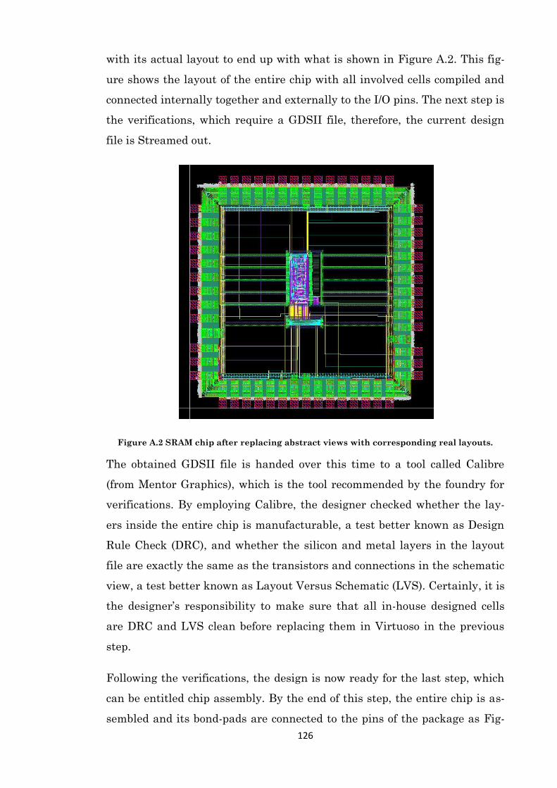
126
with its actual layout to end up with what is shown in Figure A.2. This fig-
ure shows the layout of the entire chip with all involved cells compiled and
connected internally together and externally to the I/O pins. The next step is
the verifications, which require a GDSII file, therefore, the current design
file is Streamed out.
Figure A.2 SRAM chip after replacing abstract views with corresponding real layouts.
The obtained GDSII file is handed over this time to a tool called Calibre
(from Mentor Graphics), which is the tool recommended by the foundry for
verifications. By employing Calibre, the designer checked whether the lay-
ers inside the entire chip is manufacturable, a test better known as Design
Rule Check (DRC), and whether the silicon and metal layers in the layout
file are exactly the same as the transistors and connections in the schematic
view, a test better known as Layout Versus Schematic (LVS). Certainly, it is
the designer’s responsibility to make sure that all in-house designed cells
are DRC and LVS clean before replacing them in Virtuoso in the previous
step.
Following the verifications, the design is now ready for the last step, which
can be entitled chip assembly. By the end of this step, the entire chip is as-
sembled and its bond-pads are connected to the pins of the package as Fig-
127
ure A.3 shows, where the package selected for HoliSRAM is PGA84. Finally,
the exported GDSII file is sent to IMEC for fabrications and packaging.
Figure A.3 HoliSRAM chip completely designed and packaged in PGA84.
A.2 Introduction
This appendix contains more details about the works related to the chips
fabrication and testing involved in this project.
A.3 Chip Gallery
The table below lists all the silicon chips that the researcher designs and
fabricates during his study. Explicitly, he contributes by designing and lay-
ing out the full-custom and analogue part of two pieces of silicon, which are
the HoliSRAM chip and the reference free voltage sensors. The former and
latter are fabricated using UMC 90nm and 180nm respectively. Important-
ly, both silicon dies have correct functionality according to the design goals.
In addition, he completely designed all parts of another SRAM chip using
TSMC 130nm technology.
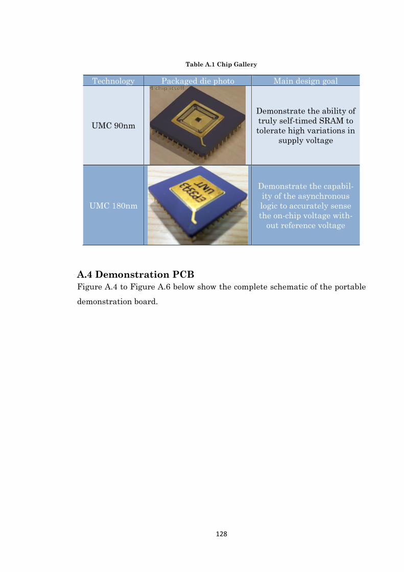
128
Table A.1 Chip Gallery
Technology Packaged die photo Main design goal
UMC 90nm
Demonstrate the ability of
truly self-timed SRAM to
tolerate high variations in
supply voltage
UMC 180nm
Demonstrate the capabil-
ity of the asynchronous
logic to accurately sense
the on-chip voltage with-
out reference voltage
A.4 Demonstration PCB
Figure A.4 to Figure A.6 below show the complete schematic of the portable
demonstration board.
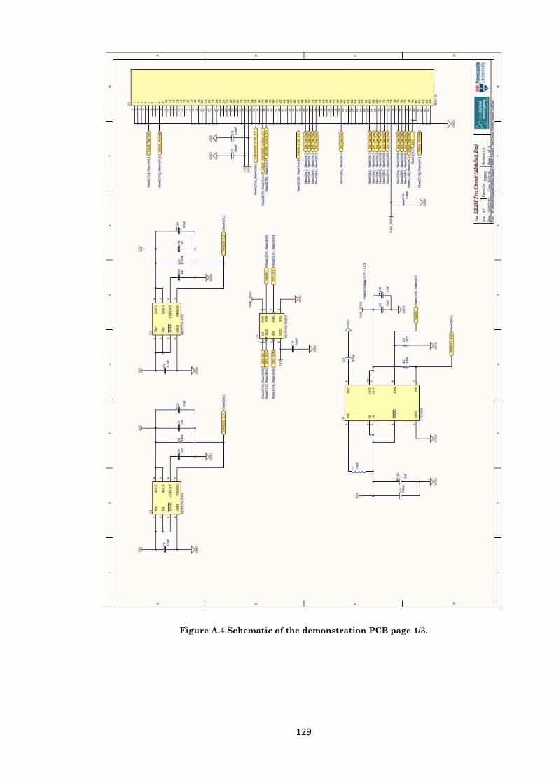
129
Figure A.4 Schematic of the demonstration PCB page 1/3.
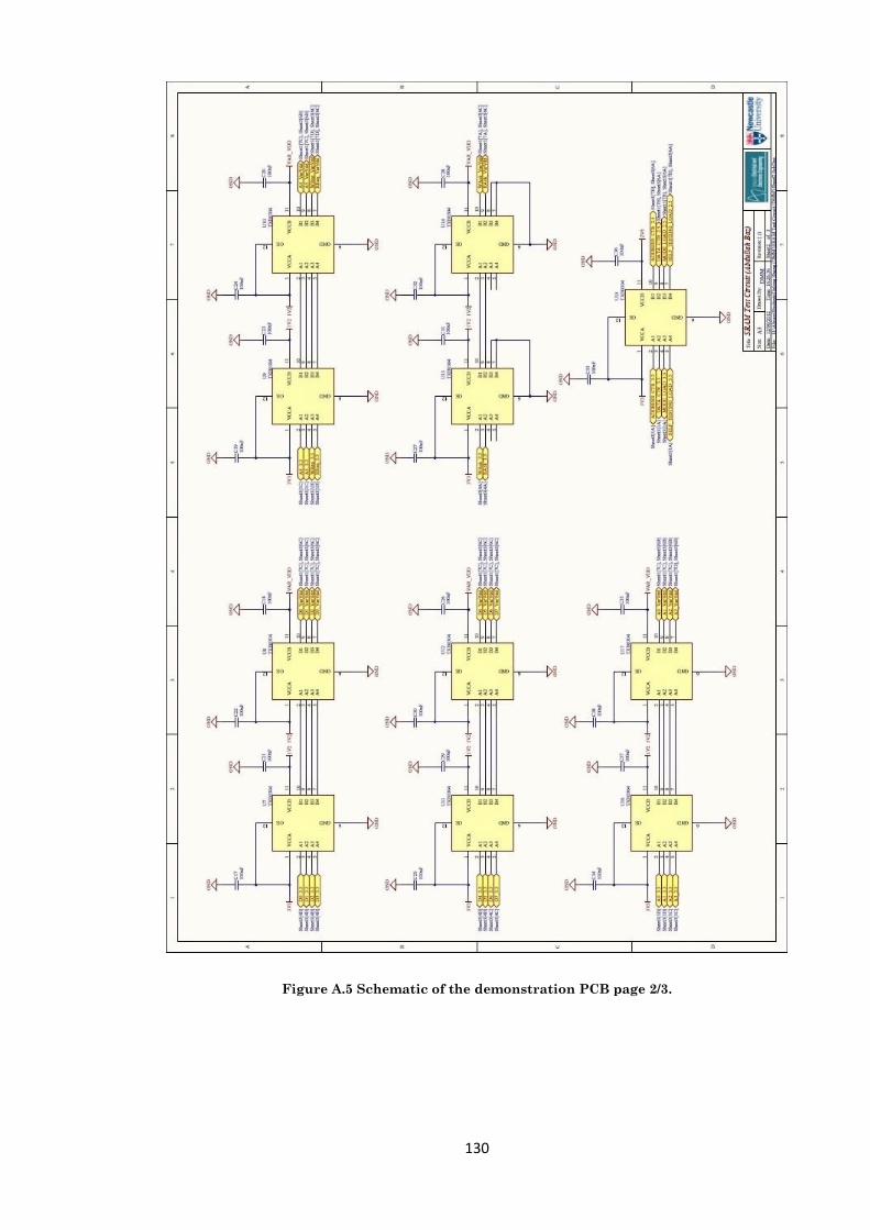
130
Figure A.5 Schematic of the demonstration PCB page 2/3.
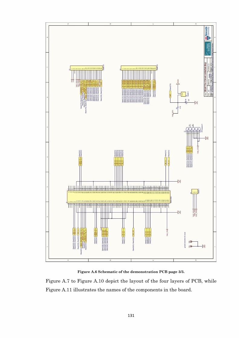
131
Figure A.6 Schematic of the demonstration PCB page 3/3.
Figure A.7 to Figure A.10 depict the layout of the four layers of PCB, while
Figure A.11 illustrates the names of the components in the board.
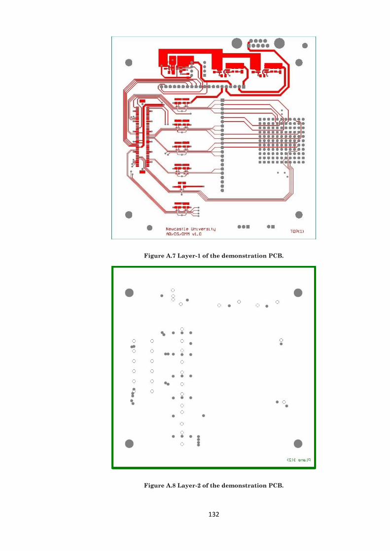
132
Figure A.7 Layer-1 of the demonstration PCB.
Figure A.8 Layer-2 of the demonstration PCB.
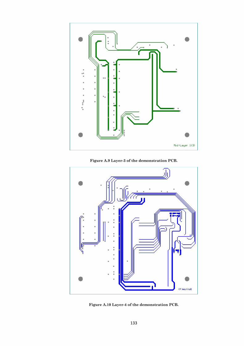
133
Figure A.9 Layer-3 of the demonstration PCB.
Figure A.10 Layer-4 of the demonstration PCB.
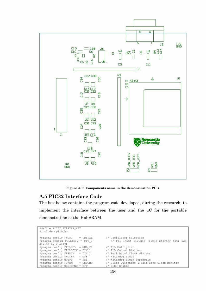
134
Figure A.11 Components name in the demonstration PCB.
A.5 PIC32 Interface Code
The box below contains the program code developed, during the research, to
implement the interface between the user and the µC for the portable
demonstration of the HoliSRAM.
#define PIC32_STARTER_KIT
#include <plib.h>
#pragma config FNOSC = PRIPLL // Oscillator Selection
#pragma config FPLLIDIV = DIV_2 // PLL Input Divider (PIC32 Starter Kit: use
divide by 2 only)
#pragma config FPLLMUL = MUL_20 // PLL Multiplier
#pragma config FPLLODIV = DIV_1 // PLL Output Divider
#pragma config FPBDIV = DIV_1 // Peripheral Clock divisor
#pragma config FWDTEN = OFF // Watchdog Timer
#pragma config WDTPS = PS1 // Watchdog Timer Postscale
#pragma config FCKSM = CSDCMD // Clock Switching & Fail Safe Clock Monitor
#pragma config OSCIOFNC = OFF // CLKO Enable
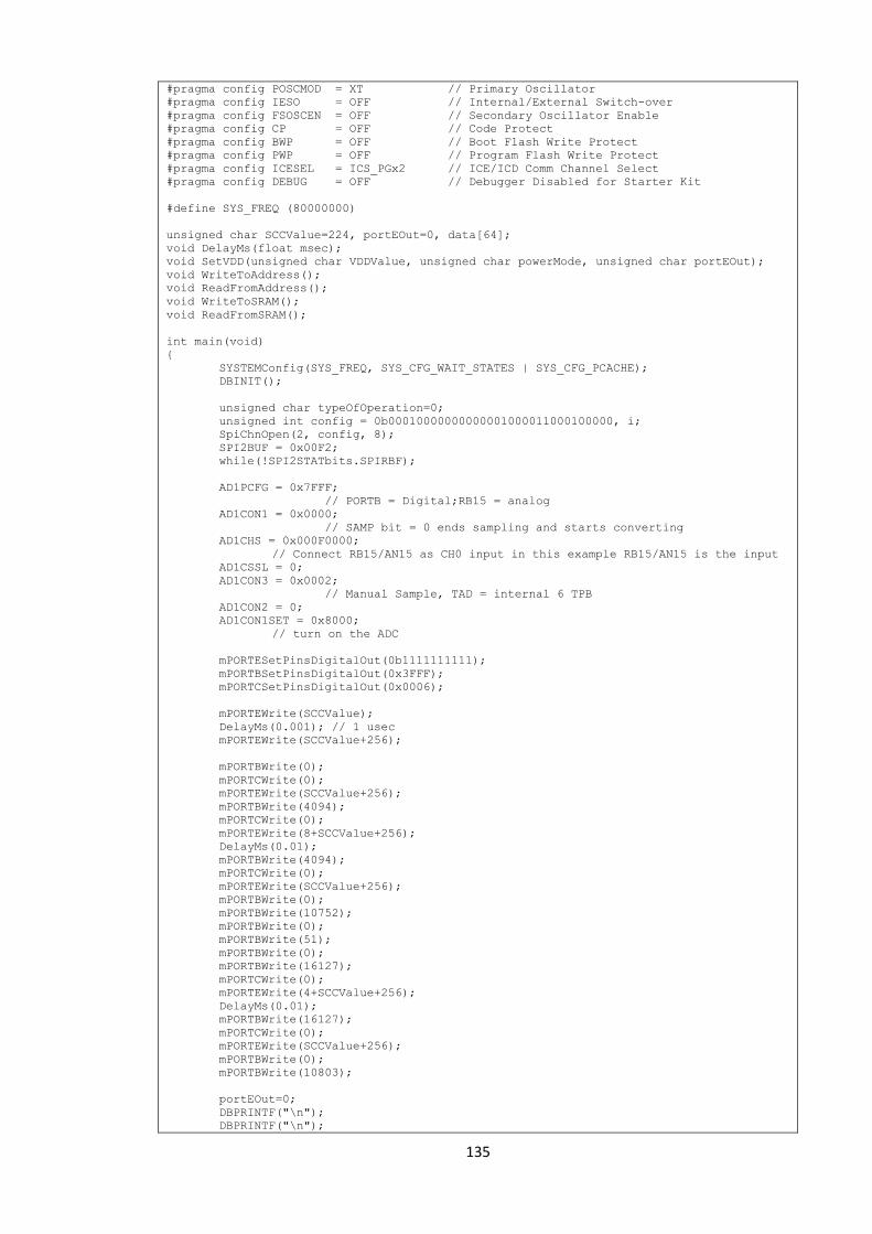
135
#pragma config POSCMOD = XT // Primary Oscillator
#pragma config IESO = OFF // Internal/External Switch-over
#pragma config FSOSCEN = OFF // Secondary Oscillator Enable
#pragma config CP = OFF // Code Protect
#pragma config BWP = OFF // Boot Flash Write Protect
#pragma config PWP = OFF // Program Flash Write Protect
#pragma config ICESEL = ICS_PGx2 // ICE/ICD Comm Channel Select
#pragma config DEBUG = OFF // Debugger Disabled for Starter Kit
#define SYS_FREQ (80000000)
unsigned char SCCValue=224, portEOut=0, data[64];
void DelayMs(float msec);
void SetVDD(unsigned char VDDValue, unsigned char powerMode, unsigned char portEOut);
void WriteToAddress();
void ReadFromAddress();
void WriteToSRAM();
void ReadFromSRAM();
int main(void)
{
SYSTEMConfig(SYS_FREQ, SYS_CFG_WAIT_STATES | SYS_CFG_PCACHE);
DBINIT();
unsigned char typeOfOperation=0;
unsigned int config = 0b00010000000000001000011000100000, i;
SpiChnOpen(2, config, 8);
SPI2BUF = 0x00F2;
while(!SPI2STATbits.SPIRBF);
AD1PCFG = 0x7FFF;
// PORTB = Digital;RB15 = analog
AD1CON1 = 0x0000;
// SAMP bit = 0 ends sampling and starts converting
AD1CHS = 0x000F0000;
// Connect RB15/AN15 as CH0 input in this example RB15/AN15 is the input
AD1CSSL = 0;
AD1CON3 = 0x0002;
// Manual Sample, TAD = internal 6 TPB
AD1CON2 = 0;
AD1CON1SET = 0x8000;
// turn on the ADC
mPORTESetPinsDigitalOut(0b1111111111);
mPORTBSetPinsDigitalOut(0x3FFF);
mPORTCSetPinsDigitalOut(0x0006);
mPORTEWrite(SCCValue);
DelayMs(0.001); // 1 usec
mPORTEWrite(SCCValue+256);
mPORTBWrite(0);
mPORTCWrite(0);
mPORTEWrite(SCCValue+256);
mPORTBWrite(4094);
mPORTCWrite(0);
mPORTEWrite(8+SCCValue+256);
DelayMs(0.01);
mPORTBWrite(4094);
mPORTCWrite(0);
mPORTEWrite(SCCValue+256);
mPORTBWrite(0);
mPORTBWrite(10752);
mPORTBWrite(0);
mPORTBWrite(51);
mPORTBWrite(0);
mPORTBWrite(16127);
mPORTCWrite(0);
mPORTEWrite(4+SCCValue+256);
DelayMs(0.01);
mPORTBWrite(16127);
mPORTCWrite(0);
mPORTEWrite(SCCValue+256);
mPORTBWrite(0);
mPORTBWrite(10803);
portEOut=0;
DBPRINTF("\n");
DBPRINTF("\n");
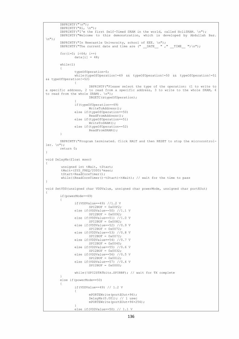
136
DBPRINTF("\n");
DBPRINTF("Hi, \n");
DBPRINTF("I'm the first Self-Timed SRAM in the world, called HoliSRAM. \n");
DBPRINTF("Welcome to this demonstration, which is developed by Abdullah Baz.
\n");
DBPRINTF("In Newcastle University, school of EEE. \n");
DBPRINTF("The current date and time are (" __DATE__ " ," __TIME__ ")\n");
for(i=0; i<64; i++)
data[i] = 48;
while(1)
{
typeOfOperation=0;
while(typeOfOperation!=49 && typeOfOperation!=50 && typeOfOperation!=51
&& typeOfOperation!=52)
{
DBPRINTF("Please select the type of the operation: (1 to write to
a specific address, 2 to read from a specific address, 3 to write to the whole SRAM, 4
to read from the whole SRAM). \n");
DBGETC(&typeOfOperation);
}
if(typeOfOperation==49)
WriteToAddress();
else if(typeOfOperation==50)
ReadFromAddress();
else if(typeOfOperation==51)
WriteToSRAM();
else if(typeOfOperation==52)
ReadFromSRAM();
}
DBPRINTF("Program terminated. Click HALT and then RESET to stop the microcontrol-
ler. \n");
return 0;
}
void DelayMs(float msec)
{
unsigned int tWait, tStart;
tWait=(SYS_FREQ/2000)*msec;
tStart=ReadCoreTimer();
while((ReadCoreTimer()-tStart)<tWait); // wait for the time to pass
}
void SetVDD(unsigned char VDDValue, unsigned char powerMode, unsigned char portEOut)
{
if(powerMode==49)
{
if(VDDValue==49) //1.2 V
SPI2BUF = 0x00F2;
else if(VDDValue==50) //1.1 V
SPI2BUF = 0x0092;
else if(VDDValue==51) //1.0 V
SPI2BUF = 0x0082;
else if(VDDValue==52) //0.9 V
SPI2BUF = 0x0072;
else if(VDDValue==53) //0.8 V
SPI2BUF = 0x0072;
else if(VDDValue==54) //0.7 V
SPI2BUF = 0x0040;
else if(VDDValue==55) //0.6 V
SPI2BUF = 0x0032;
else if(VDDValue==56) //0.5 V
SPI2BUF = 0x0012;
else if(VDDValue==57) //0.4 V
SPI2BUF = 0x0000;
while(!SPI2STATbits.SPIRBF); // wait for TX complete
}
else if(powerMode==50)
{
if(VDDValue==49) // 1.2 V
{
mPORTEWrite(portEOut+96);
DelayMs(0.001); // 1 usec
mPORTEWrite(portEOut+96+256);
}
else if(VDDValue==50) // 1.1 V
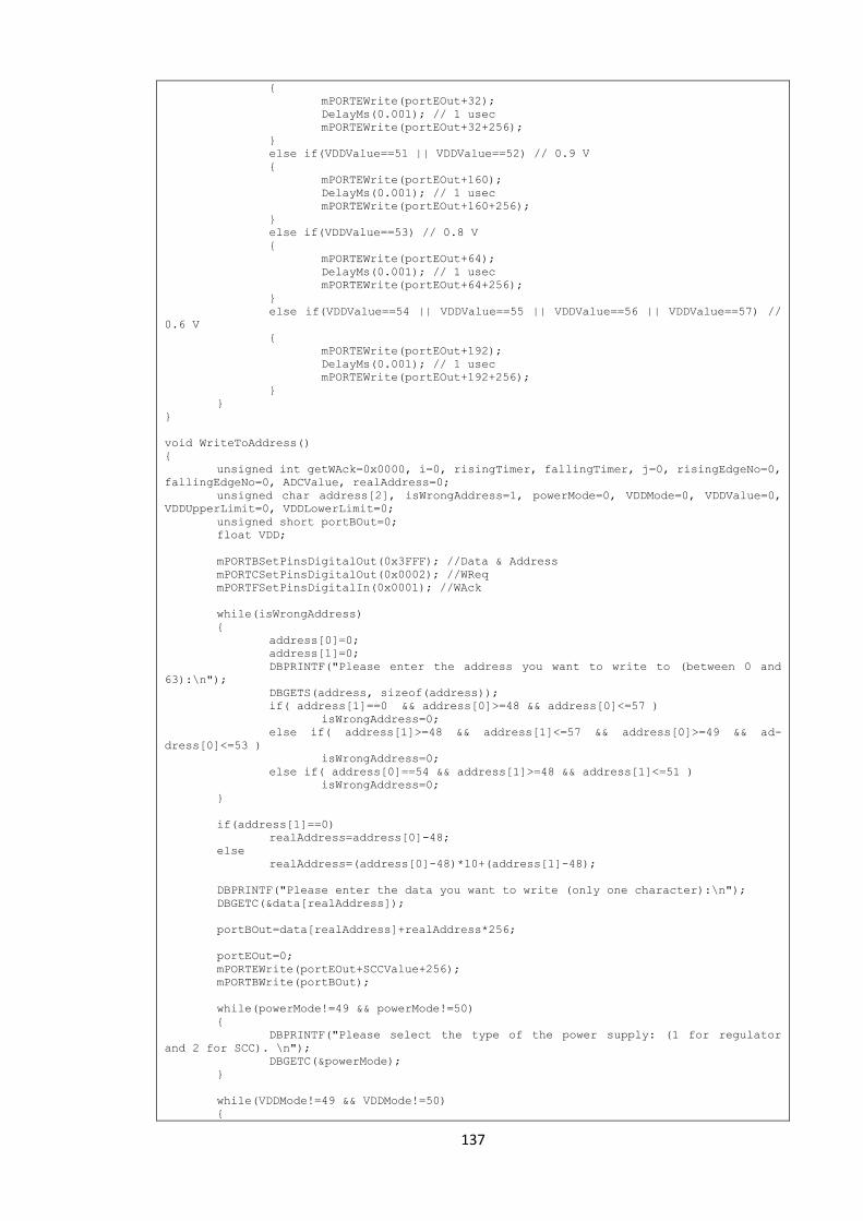
137
{
mPORTEWrite(portEOut+32);
DelayMs(0.001); // 1 usec
mPORTEWrite(portEOut+32+256);
}
else if(VDDValue==51 || VDDValue==52) // 0.9 V
{
mPORTEWrite(portEOut+160);
DelayMs(0.001); // 1 usec
mPORTEWrite(portEOut+160+256);
}
else if(VDDValue==53) // 0.8 V
{
mPORTEWrite(portEOut+64);
DelayMs(0.001); // 1 usec
mPORTEWrite(portEOut+64+256);
}
else if(VDDValue==54 || VDDValue==55 || VDDValue==56 || VDDValue==57) //
0.6 V
{
mPORTEWrite(portEOut+192);
DelayMs(0.001); // 1 usec
mPORTEWrite(portEOut+192+256);
}
}
}
void WriteToAddress()
{
unsigned int getWAck=0x0000, i=0, risingTimer, fallingTimer, j=0, risingEdgeNo=0,
fallingEdgeNo=0, ADCValue, realAddress=0;
unsigned char address[2], isWrongAddress=1, powerMode=0, VDDMode=0, VDDValue=0,
VDDUpperLimit=0, VDDLowerLimit=0;
unsigned short portBOut=0;
float VDD;
mPORTBSetPinsDigitalOut(0x3FFF); //Data & Address
mPORTCSetPinsDigitalOut(0x0002); //WReq
mPORTFSetPinsDigitalIn(0x0001); //WAck
while(isWrongAddress)
{
address[0]=0;
address[1]=0;
DBPRINTF("Please enter the address you want to write to (between 0 and
63):\n");
DBGETS(address, sizeof(address));
if( address[1]==0 && address[0]>=48 && address[0]<=57 )
isWrongAddress=0;
else if( address[1]>=48 && address[1]<=57 && address[0]>=49 && ad-
dress[0]<=53 )
isWrongAddress=0;
else if( address[0]==54 && address[1]>=48 && address[1]<=51 )
isWrongAddress=0;
}
if(address[1]==0)
realAddress=address[0]-48;
else
realAddress=(address[0]-48)*10+(address[1]-48);
DBPRINTF("Please enter the data you want to write (only one character):\n");
DBGETC(&data[realAddress]);
portBOut=data[realAddress]+realAddress*256;
portEOut=0;
mPORTEWrite(portEOut+SCCValue+256);
mPORTBWrite(portBOut);
while(powerMode!=49 && powerMode!=50)
{
DBPRINTF("Please select the type of the power supply: (1 for regulator
and 2 for SCC). \n");
DBGETC(&powerMode);
}
while(VDDMode!=49 && VDDMode!=50)
{
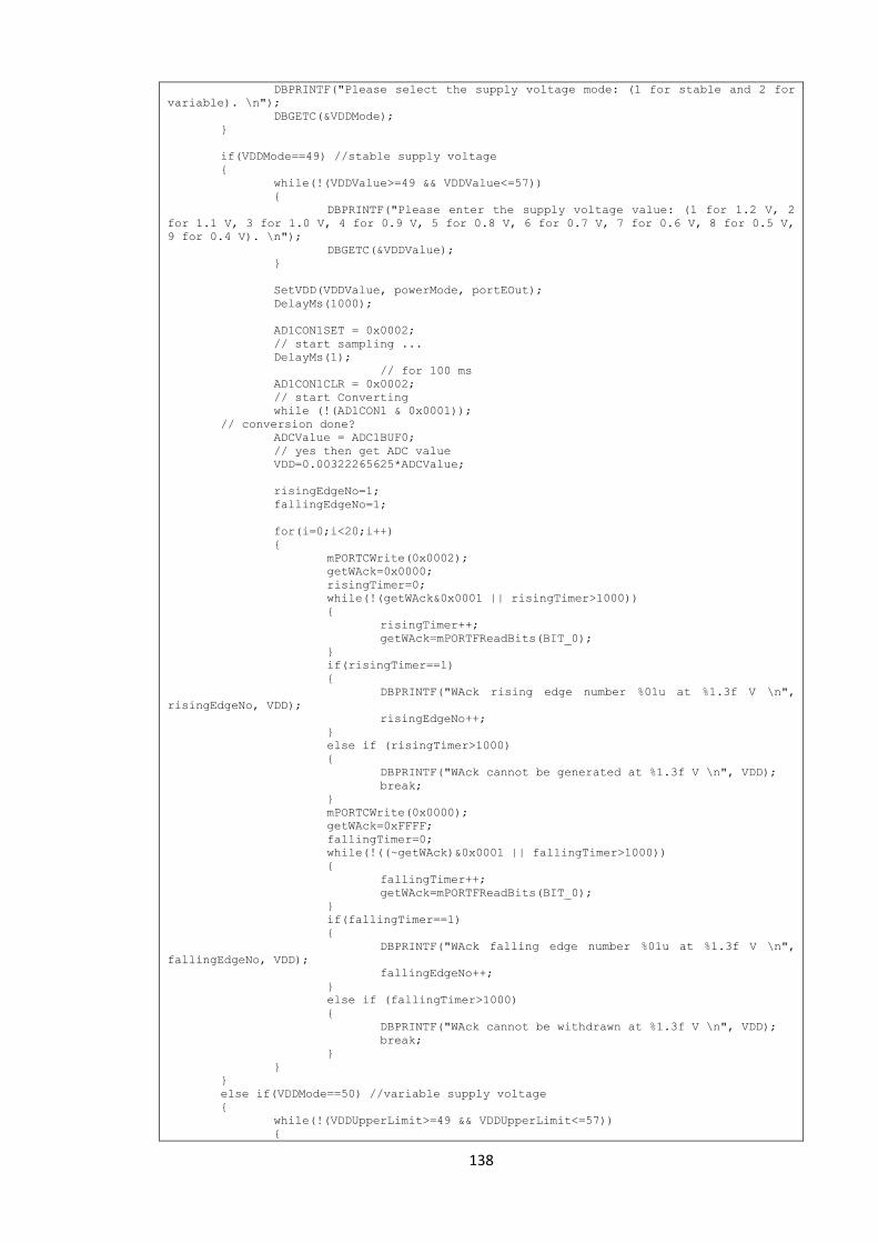
138
DBPRINTF("Please select the supply voltage mode: (1 for stable and 2 for
variable). \n");
DBGETC(&VDDMode);
}
if(VDDMode==49) //stable supply voltage
{
while(!(VDDValue>=49 && VDDValue<=57))
{
DBPRINTF("Please enter the supply voltage value: (1 for 1.2 V, 2
for 1.1 V, 3 for 1.0 V, 4 for 0.9 V, 5 for 0.8 V, 6 for 0.7 V, 7 for 0.6 V, 8 for 0.5 V,
9 for 0.4 V). \n");
DBGETC(&VDDValue);
}
SetVDD(VDDValue, powerMode, portEOut);
DelayMs(1000);
AD1CON1SET = 0x0002;
// start sampling ...
DelayMs(1);
// for 100 ms
AD1CON1CLR = 0x0002;
// start Converting
while (!(AD1CON1 & 0x0001));
// conversion done?
ADCValue = ADC1BUF0;
// yes then get ADC value
VDD=0.00322265625*ADCValue;
risingEdgeNo=1;
fallingEdgeNo=1;
for(i=0;i<20;i++)
{
mPORTCWrite(0x0002);
getWAck=0x0000;
risingTimer=0;
while(!(getWAck&0x0001 || risingTimer>1000))
{
risingTimer++;
getWAck=mPORTFReadBits(BIT_0);
}
if(risingTimer==1)
{
DBPRINTF("WAck rising edge number %01u at %1.3f V \n",
risingEdgeNo, VDD);
risingEdgeNo++;
}
else if (risingTimer>1000)
{
DBPRINTF("WAck cannot be generated at %1.3f V \n", VDD);
break;
}
mPORTCWrite(0x0000);
getWAck=0xFFFF;
fallingTimer=0;
while(!((~getWAck)&0x0001 || fallingTimer>1000))
{
fallingTimer++;
getWAck=mPORTFReadBits(BIT_0);
}
if(fallingTimer==1)
{
DBPRINTF("WAck falling edge number %01u at %1.3f V \n",
fallingEdgeNo, VDD);
fallingEdgeNo++;
}
else if (fallingTimer>1000)
{
DBPRINTF("WAck cannot be withdrawn at %1.3f V \n", VDD);
break;
}
}
}
else if(VDDMode==50) //variable supply voltage
{
while(!(VDDUpperLimit>=49 && VDDUpperLimit<=57))
{
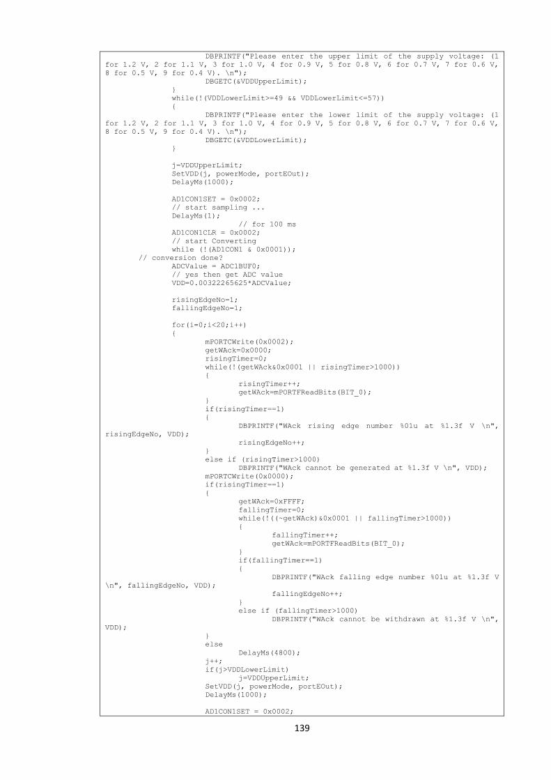
139
DBPRINTF("Please enter the upper limit of the supply voltage: (1
for 1.2 V, 2 for 1.1 V, 3 for 1.0 V, 4 for 0.9 V, 5 for 0.8 V, 6 for 0.7 V, 7 for 0.6 V,
8 for 0.5 V, 9 for 0.4 V). \n");
DBGETC(&VDDUpperLimit);
}
while(!(VDDLowerLimit>=49 && VDDLowerLimit<=57))
{
DBPRINTF("Please enter the lower limit of the supply voltage: (1
for 1.2 V, 2 for 1.1 V, 3 for 1.0 V, 4 for 0.9 V, 5 for 0.8 V, 6 for 0.7 V, 7 for 0.6 V,
8 for 0.5 V, 9 for 0.4 V). \n");
DBGETC(&VDDLowerLimit);
}
j=VDDUpperLimit;
SetVDD(j, powerMode, portEOut);
DelayMs(1000);
AD1CON1SET = 0x0002;
// start sampling ...
DelayMs(1);
// for 100 ms
AD1CON1CLR = 0x0002;
// start Converting
while (!(AD1CON1 & 0x0001));
// conversion done?
ADCValue = ADC1BUF0;
// yes then get ADC value
VDD=0.00322265625*ADCValue;
risingEdgeNo=1;
fallingEdgeNo=1;
for(i=0;i<20;i++)
{
mPORTCWrite(0x0002);
getWAck=0x0000;
risingTimer=0;
while(!(getWAck&0x0001 || risingTimer>1000))
{
risingTimer++;
getWAck=mPORTFReadBits(BIT_0);
}
if(risingTimer==1)
{
DBPRINTF("WAck rising edge number %01u at %1.3f V \n",
risingEdgeNo, VDD);
risingEdgeNo++;
}
else if (risingTimer>1000)
DBPRINTF("WAck cannot be generated at %1.3f V \n", VDD);
mPORTCWrite(0x0000);
if(risingTimer==1)
{
getWAck=0xFFFF;
fallingTimer=0;
while(!((~getWAck)&0x0001 || fallingTimer>1000))
{
fallingTimer++;
getWAck=mPORTFReadBits(BIT_0);
}
if(fallingTimer==1)
{
DBPRINTF("WAck falling edge number %01u at %1.3f V
\n", fallingEdgeNo, VDD);
fallingEdgeNo++;
}
else if (fallingTimer>1000)
DBPRINTF("WAck cannot be withdrawn at %1.3f V \n",
VDD);
}
else
DelayMs(4800);
j++;
if(j>VDDLowerLimit)
j=VDDUpperLimit;
SetVDD(j, powerMode, portEOut);
DelayMs(1000);
AD1CON1SET = 0x0002;
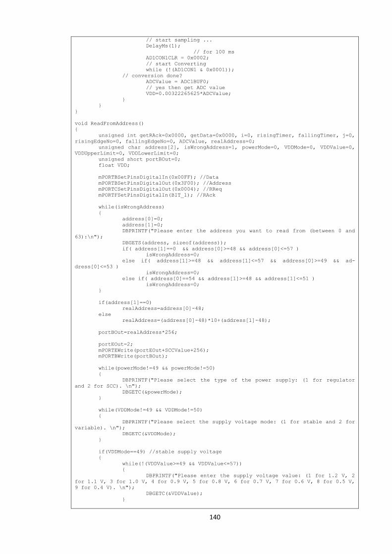
140
// start sampling ...
DelayMs(1);
// for 100 ms
AD1CON1CLR = 0x0002;
// start Converting
while (!(AD1CON1 & 0x0001));
// conversion done?
ADCValue = ADC1BUF0;
// yes then get ADC value
VDD=0.00322265625*ADCValue;
}
}
}
void ReadFromAddress()
{
unsigned int getRAck=0x0000, getData=0x0000, i=0, risingTimer, fallingTimer, j=0,
risingEdgeNo=0, fallingEdgeNo=0, ADCValue, realAddress=0;
unsigned char address[2], isWrongAddress=1, powerMode=0, VDDMode=0, VDDValue=0,
VDDUpperLimit=0, VDDLowerLimit=0;
unsigned short portBOut=0;
float VDD;
mPORTBSetPinsDigitalIn(0x00FF); //Data
mPORTBSetPinsDigitalOut(0x3F00); //Address
mPORTCSetPinsDigitalOut(0x0004); //RReq
mPORTFSetPinsDigitalIn(BIT_1); //RAck
while(isWrongAddress)
{
address[0]=0;
address[1]=0;
DBPRINTF("Please enter the address you want to read from (between 0 and
63):\n");
DBGETS(address, sizeof(address));
if( address[1]==0 && address[0]>=48 && address[0]<=57 )
isWrongAddress=0;
else if( address[1]>=48 && address[1]<=57 && address[0]>=49 && ad-
dress[0]<=53 )
isWrongAddress=0;
else if( address[0]==54 && address[1]>=48 && address[1]<=51 )
isWrongAddress=0;
}
if(address[1]==0)
realAddress=address[0]-48;
else
realAddress=(address[0]-48)*10+(address[1]-48);
portBOut=realAddress*256;
portEOut=2;
mPORTEWrite(portEOut+SCCValue+256);
mPORTBWrite(portBOut);
while(powerMode!=49 && powerMode!=50)
{
DBPRINTF("Please select the type of the power supply: (1 for regulator
and 2 for SCC). \n");
DBGETC(&powerMode);
}
while(VDDMode!=49 && VDDMode!=50)
{
DBPRINTF("Please select the supply voltage mode: (1 for stable and 2 for
variable). \n");
DBGETC(&VDDMode);
}
if(VDDMode==49) //stable supply voltage
{
while(!(VDDValue>=49 && VDDValue<=57))
{
DBPRINTF("Please enter the supply voltage value: (1 for 1.2 V, 2
for 1.1 V, 3 for 1.0 V, 4 for 0.9 V, 5 for 0.8 V, 6 for 0.7 V, 7 for 0.6 V, 8 for 0.5 V,
9 for 0.4 V). \n");
DBGETC(&VDDValue);
}
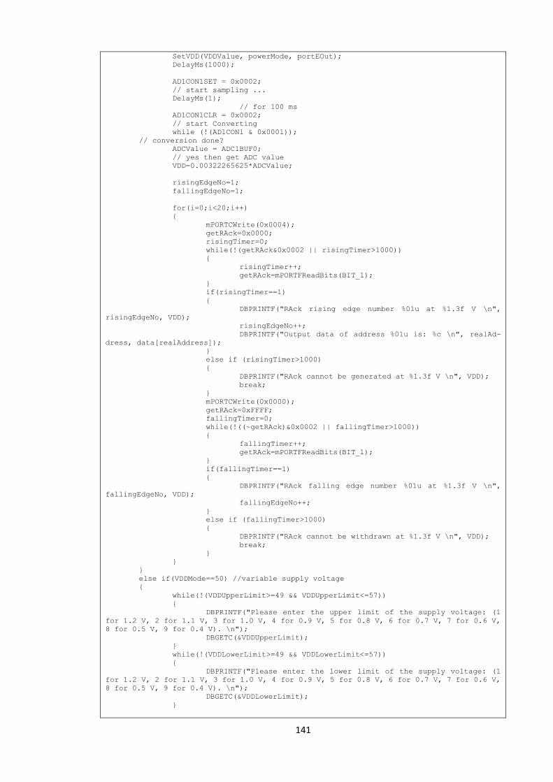
141
SetVDD(VDDValue, powerMode, portEOut);
DelayMs(1000);
AD1CON1SET = 0x0002;
// start sampling ...
DelayMs(1);
// for 100 ms
AD1CON1CLR = 0x0002;
// start Converting
while (!(AD1CON1 & 0x0001));
// conversion done?
ADCValue = ADC1BUF0;
// yes then get ADC value
VDD=0.00322265625*ADCValue;
risingEdgeNo=1;
fallingEdgeNo=1;
for(i=0;i<20;i++)
{
mPORTCWrite(0x0004);
getRAck=0x0000;
risingTimer=0;
while(!(getRAck&0x0002 || risingTimer>1000))
{
risingTimer++;
getRAck=mPORTFReadBits(BIT_1);
}
if(risingTimer==1)
{
DBPRINTF("RAck rising edge number %01u at %1.3f V \n",
risingEdgeNo, VDD);
risingEdgeNo++;
DBPRINTF("Output data of address %01u is: %c \n", realAd-
dress, data[realAddress]);
}
else if (risingTimer>1000)
{
DBPRINTF("RAck cannot be generated at %1.3f V \n", VDD);
break;
}
mPORTCWrite(0x0000);
getRAck=0xFFFF;
fallingTimer=0;
while(!((~getRAck)&0x0002 || fallingTimer>1000))
{
fallingTimer++;
getRAck=mPORTFReadBits(BIT_1);
}
if(fallingTimer==1)
{
DBPRINTF("RAck falling edge number %01u at %1.3f V \n",
fallingEdgeNo, VDD);
fallingEdgeNo++;
}
else if (fallingTimer>1000)
{
DBPRINTF("RAck cannot be withdrawn at %1.3f V \n", VDD);
break;
}
}
}
else if(VDDMode==50) //variable supply voltage
{
while(!(VDDUpperLimit>=49 && VDDUpperLimit<=57))
{
DBPRINTF("Please enter the upper limit of the supply voltage: (1
for 1.2 V, 2 for 1.1 V, 3 for 1.0 V, 4 for 0.9 V, 5 for 0.8 V, 6 for 0.7 V, 7 for 0.6 V,
8 for 0.5 V, 9 for 0.4 V). \n");
DBGETC(&VDDUpperLimit);
}
while(!(VDDLowerLimit>=49 && VDDLowerLimit<=57))
{
DBPRINTF("Please enter the lower limit of the supply voltage: (1
for 1.2 V, 2 for 1.1 V, 3 for 1.0 V, 4 for 0.9 V, 5 for 0.8 V, 6 for 0.7 V, 7 for 0.6 V,
8 for 0.5 V, 9 for 0.4 V). \n");
DBGETC(&VDDLowerLimit);
}
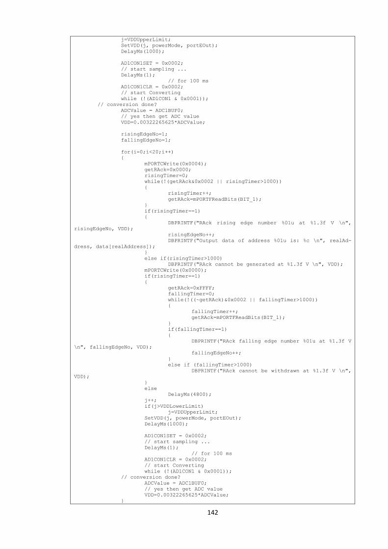
142
j=VDDUpperLimit;
SetVDD(j, powerMode, portEOut);
DelayMs(1000);
AD1CON1SET = 0x0002;
// start sampling ...
DelayMs(1);
// for 100 ms
AD1CON1CLR = 0x0002;
// start Converting
while (!(AD1CON1 & 0x0001));
// conversion done?
ADCValue = ADC1BUF0;
// yes then get ADC value
VDD=0.00322265625*ADCValue;
risingEdgeNo=1;
fallingEdgeNo=1;
for(i=0;i<20;i++)
{
mPORTCWrite(0x0004);
getRAck=0x0000;
risingTimer=0;
while(!(getRAck&0x0002 || risingTimer>1000))
{
risingTimer++;
getRAck=mPORTFReadBits(BIT_1);
}
if(risingTimer==1)
{
DBPRINTF("RAck rising edge number %01u at %1.3f V \n",
risingEdgeNo, VDD);
risingEdgeNo++;
DBPRINTF("Output data of address %01u is: %c \n", realAd-
dress, data[realAddress]);
}
else if(risingTimer>1000)
DBPRINTF("RAck cannot be generated at %1.3f V \n", VDD);
mPORTCWrite(0x0000);
if(risingTimer==1)
{
getRAck=0xFFFF;
fallingTimer=0;
while(!((~getRAck)&0x0002 || fallingTimer>1000))
{
fallingTimer++;
getRAck=mPORTFReadBits(BIT_1);
}
if(fallingTimer==1)
{
DBPRINTF("RAck falling edge number %01u at %1.3f V
\n", fallingEdgeNo, VDD);
fallingEdgeNo++;
}
else if (fallingTimer>1000)
DBPRINTF("RAck cannot be withdrawn at %1.3f V \n",
VDD);
}
else
DelayMs(4800);
j++;
if(j>VDDLowerLimit)
j=VDDUpperLimit;
SetVDD(j, powerMode, portEOut);
DelayMs(1000);
AD1CON1SET = 0x0002;
// start sampling ...
DelayMs(1);
// for 100 ms
AD1CON1CLR = 0x0002;
// start Converting
while (!(AD1CON1 & 0x0001));
// conversion done?
ADCValue = ADC1BUF0;
// yes then get ADC value
VDD=0.00322265625*ADCValue;
}
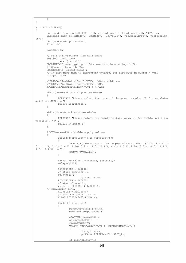
143
}
}
void WriteToSRAM()
{
unsigned int getWAck=0x0000, i=0, risingTimer, fallingTimer, j=0, ADCValue;
unsigned char powerMode=0, VDDMode=0, VDDValue=0, VDDUpperLimit=0, VDDLowerLim-
it=0;
unsigned short portBOut=0;
float VDD;
portEOut=0;
// Fill string buffer with null chars
for(i=0; i<64; i++)
data[i] = '\0';
DBPRINTF("Please type up to 64 characters long string. \n");
// Store it in our buffer
DBGETS(data, sizeof(data));
// In case more than 64 characters entered, set last byte in buffer = null
data[64] = 0;
mPORTBSetPinsDigitalOut(0x3FFF); //Data & Address
mPORTCSetPinsDigitalOut(0x0002); //WReq
mPORTFSetPinsDigitalIn(0x0001); //WAck
while(powerMode!=49 && powerMode!=50)
{
DBPRINTF("Please select the type of the power supply: (1 for regulator
and 2 for SCC). \n");
DBGETC(&powerMode);
}
while(VDDMode!=49 && VDDMode!=50)
{
DBPRINTF("Please select the supply voltage mode: (1 for stable and 2 for
variable). \n");
DBGETC(&VDDMode);
}
if(VDDMode==49) //stable supply voltage
{
while(!(VDDValue>=49 && VDDValue<=57))
{
DBPRINTF("Please enter the supply voltage value: (1 for 1.2 V, 2
for 1.1 V, 3 for 1.0 V, 4 for 0.9 V, 5 for 0.8 V, 6 for 0.7 V, 7 for 0.6 V, 8 for 0.5 V,
9 for 0.4 V). \n");
DBGETC(&VDDValue);
}
SetVDD(VDDValue, powerMode, portEOut);
DelayMs(1000);
AD1CON1SET = 0x0002;
// start sampling ...
DelayMs(1);
// for 100 ms
AD1CON1CLR = 0x0002;
// start Converting
while (!(AD1CON1 & 0x0001));
// conversion done?
ADCValue = ADC1BUF0;
// yes then get ADC value
VDD=0.00322265625*ADCValue;
for(i=0; i<64; i++)
{
portBOut=data[i]+i*256;
mPORTBWrite(portBOut);
mPORTCWrite(0x0002);
getWAck=0x0000;
risingTimer=0;
while(!(getWAck&0x0001 || risingTimer>1000))
{
risingTimer++;
getWAck=mPORTFReadBits(BIT_0);
}
if(risingTimer==1)
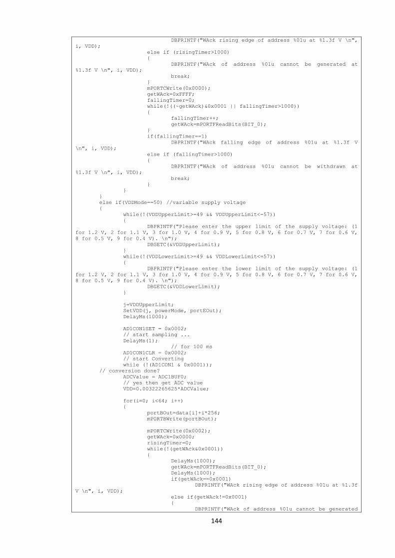
144
DBPRINTF("WAck rising edge of address %01u at %1.3f V \n",
i, VDD);
else if (risingTimer>1000)
{
DBPRINTF("WAck of address %01u cannot be generated at
%1.3f V \n", i, VDD);
break;
}
mPORTCWrite(0x0000);
getWAck=0xFFFF;
fallingTimer=0;
while(!((~getWAck)&0x0001 || fallingTimer>1000))
{
fallingTimer++;
getWAck=mPORTFReadBits(BIT_0);
}
if(fallingTimer==1)
DBPRINTF("WAck falling edge of address %01u at %1.3f V
\n", i, VDD);
else if (fallingTimer>1000)
{
DBPRINTF("WAck of address %01u cannot be withdrawn at
%1.3f V \n", i, VDD);
break;
}
}
}
else if(VDDMode==50) //variable supply voltage
{
while(!(VDDUpperLimit>=49 && VDDUpperLimit<=57))
{
DBPRINTF("Please enter the upper limit of the supply voltage: (1
for 1.2 V, 2 for 1.1 V, 3 for 1.0 V, 4 for 0.9 V, 5 for 0.8 V, 6 for 0.7 V, 7 for 0.6 V,
8 for 0.5 V, 9 for 0.4 V). \n");
DBGETC(&VDDUpperLimit);
}
while(!(VDDLowerLimit>=49 && VDDLowerLimit<=57))
{
DBPRINTF("Please enter the lower limit of the supply voltage: (1
for 1.2 V, 2 for 1.1 V, 3 for 1.0 V, 4 for 0.9 V, 5 for 0.8 V, 6 for 0.7 V, 7 for 0.6 V,
8 for 0.5 V, 9 for 0.4 V). \n");
DBGETC(&VDDLowerLimit);
}
j=VDDUpperLimit;
SetVDD(j, powerMode, portEOut);
DelayMs(1000);
AD1CON1SET = 0x0002;
// start sampling ...
DelayMs(1);
// for 100 ms
AD1CON1CLR = 0x0002;
// start Converting
while (!(AD1CON1 & 0x0001));
// conversion done?
ADCValue = ADC1BUF0;
// yes then get ADC value
VDD=0.00322265625*ADCValue;
for(i=0; i<64; i++)
{
portBOut=data[i]+i*256;
mPORTBWrite(portBOut);
mPORTCWrite(0x0002);
getWAck=0x0000;
risingTimer=0;
while(!(getWAck&0x0001))
{
DelayMs(1000);
getWAck=mPORTFReadBits(BIT_0);
DelayMs(1000);
if(getWAck==0x0001)
DBPRINTF("WAck rising edge of address %01u at %1.3f
V \n", i, VDD);
else if(getWAck!=0x0001)
{
DBPRINTF("WAck of address %01u cannot be generated
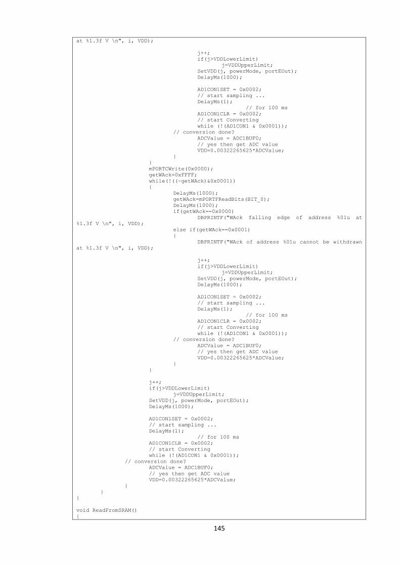
145
at %1.3f V \n", i, VDD);
j++;
if(j>VDDLowerLimit)
j=VDDUpperLimit;
SetVDD(j, powerMode, portEOut);
DelayMs(1000);
AD1CON1SET = 0x0002;
// start sampling ...
DelayMs(1);
// for 100 ms
AD1CON1CLR = 0x0002;
// start Converting
while (!(AD1CON1 & 0x0001));
// conversion done?
ADCValue = ADC1BUF0;
// yes then get ADC value
VDD=0.00322265625*ADCValue;
}
}
mPORTCWrite(0x0000);
getWAck=0xFFFF;
while(!((~getWAck)&0x0001))
{
DelayMs(1000);
getWAck=mPORTFReadBits(BIT_0);
DelayMs(1000);
if(getWAck==0x0000)
DBPRINTF("WAck falling edge of address %01u at
%1.3f V \n", i, VDD);
else if(getWAck==0x0001)
{
DBPRINTF("WAck of address %01u cannot be withdrawn
at %1.3f V \n", i, VDD);
j++;
if(j>VDDLowerLimit)
j=VDDUpperLimit;
SetVDD(j, powerMode, portEOut);
DelayMs(1000);
AD1CON1SET = 0x0002;
// start sampling ...
DelayMs(1);
// for 100 ms
AD1CON1CLR = 0x0002;
// start Converting
while (!(AD1CON1 & 0x0001));
// conversion done?
ADCValue = ADC1BUF0;
// yes then get ADC value
VDD=0.00322265625*ADCValue;
}
}
}
void ReadFromSRAM()
{
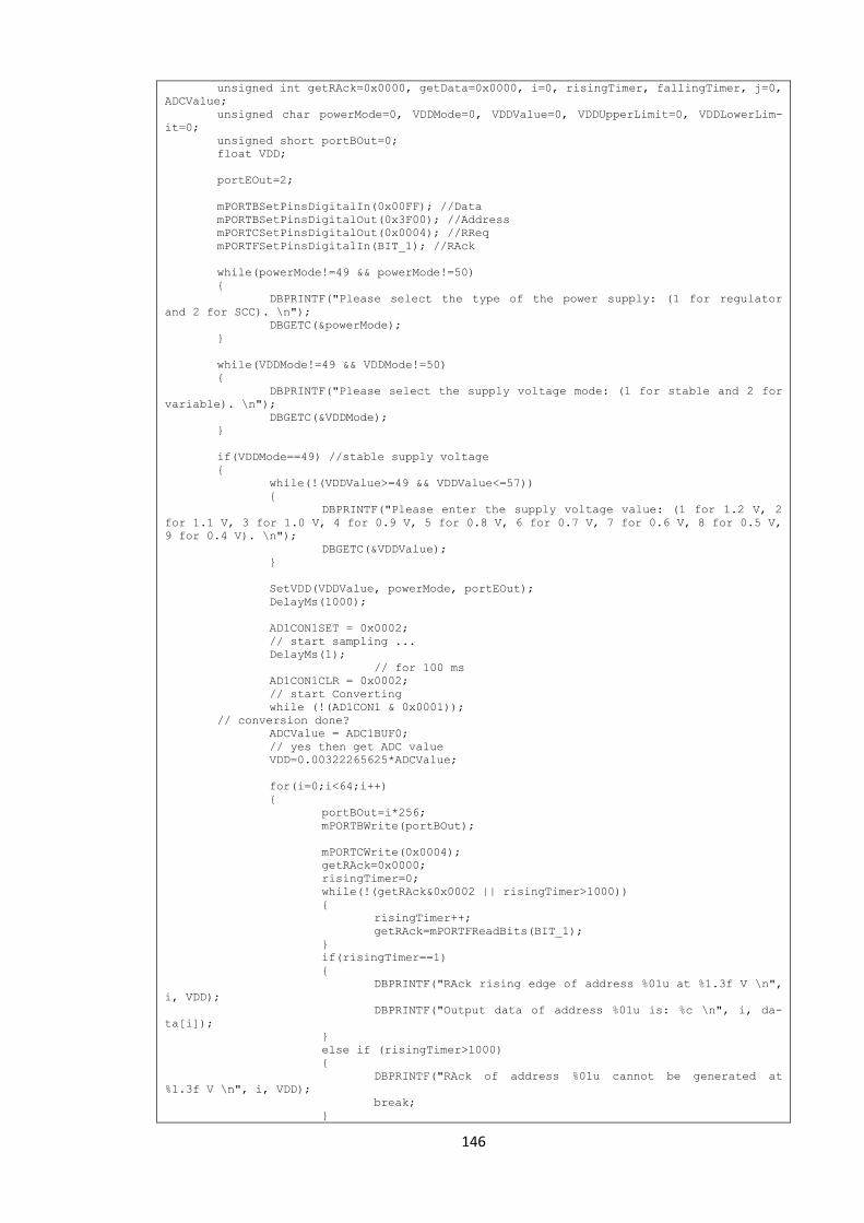
146
unsigned int getRAck=0x0000, getData=0x0000, i=0, risingTimer, fallingTimer, j=0,
ADCValue;
unsigned char powerMode=0, VDDMode=0, VDDValue=0, VDDUpperLimit=0, VDDLowerLim-
it=0;
unsigned short portBOut=0;
float VDD;
portEOut=2;
mPORTBSetPinsDigitalIn(0x00FF); //Data
mPORTBSetPinsDigitalOut(0x3F00); //Address
mPORTCSetPinsDigitalOut(0x0004); //RReq
mPORTFSetPinsDigitalIn(BIT_1); //RAck
while(powerMode!=49 && powerMode!=50)
{
DBPRINTF("Please select the type of the power supply: (1 for regulator
and 2 for SCC). \n");
DBGETC(&powerMode);
}
while(VDDMode!=49 && VDDMode!=50)
{
DBPRINTF("Please select the supply voltage mode: (1 for stable and 2 for
variable). \n");
DBGETC(&VDDMode);
}
if(VDDMode==49) //stable supply voltage
{
while(!(VDDValue>=49 && VDDValue<=57))
{
DBPRINTF("Please enter the supply voltage value: (1 for 1.2 V, 2
for 1.1 V, 3 for 1.0 V, 4 for 0.9 V, 5 for 0.8 V, 6 for 0.7 V, 7 for 0.6 V, 8 for 0.5 V,
9 for 0.4 V). \n");
DBGETC(&VDDValue);
}
SetVDD(VDDValue, powerMode, portEOut);
DelayMs(1000);
AD1CON1SET = 0x0002;
// start sampling ...
DelayMs(1);
// for 100 ms
AD1CON1CLR = 0x0002;
// start Converting
while (!(AD1CON1 & 0x0001));
// conversion done?
ADCValue = ADC1BUF0;
// yes then get ADC value
VDD=0.00322265625*ADCValue;
for(i=0;i<64;i++)
{
portBOut=i*256;
mPORTBWrite(portBOut);
mPORTCWrite(0x0004);
getRAck=0x0000;
risingTimer=0;
while(!(getRAck&0x0002 || risingTimer>1000))
{
risingTimer++;
getRAck=mPORTFReadBits(BIT_1);
}
if(risingTimer==1)
{
DBPRINTF("RAck rising edge of address %01u at %1.3f V \n",
i, VDD);
DBPRINTF("Output data of address %01u is: %c \n", i, da-
ta[i]);
}
else if (risingTimer>1000)
{
DBPRINTF("RAck of address %01u cannot be generated at
%1.3f V \n", i, VDD);
break;
}
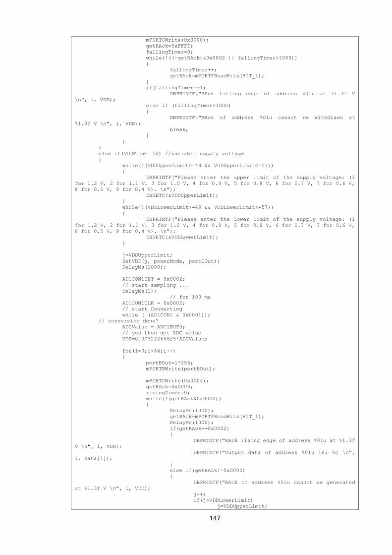
147
mPORTCWrite(0x0000);
getRAck=0xFFFF;
fallingTimer=0;
while(!((~getRAck)&0x0002 || fallingTimer>1000))
{
fallingTimer++;
getRAck=mPORTFReadBits(BIT_1);
}
if(fallingTimer==1)
DBPRINTF("RAck falling edge of address %01u at %1.3f V
\n", i, VDD);
else if (fallingTimer>1000)
{
DBPRINTF("RAck of address %01u cannot be withdrawn at
%1.3f V \n", i, VDD);
break;
}
}
}
else if(VDDMode==50) //variable supply voltage
{
while(!(VDDUpperLimit>=49 && VDDUpperLimit<=57))
{
DBPRINTF("Please enter the upper limit of the supply voltage: (1
for 1.2 V, 2 for 1.1 V, 3 for 1.0 V, 4 for 0.9 V, 5 for 0.8 V, 6 for 0.7 V, 7 for 0.6 V,
8 for 0.5 V, 9 for 0.4 V). \n");
DBGETC(&VDDUpperLimit);
}
while(!(VDDLowerLimit>=49 && VDDLowerLimit<=57))
{
DBPRINTF("Please enter the lower limit of the supply voltage: (1
for 1.2 V, 2 for 1.1 V, 3 for 1.0 V, 4 for 0.9 V, 5 for 0.8 V, 6 for 0.7 V, 7 for 0.6 V,
8 for 0.5 V, 9 for 0.4 V). \n");
DBGETC(&VDDLowerLimit);
}
j=VDDUpperLimit;
SetVDD(j, powerMode, portEOut);
DelayMs(1000);
AD1CON1SET = 0x0002;
// start sampling ...
DelayMs(1);
// for 100 ms
AD1CON1CLR = 0x0002;
// start Converting
while (!(AD1CON1 & 0x0001));
// conversion done?
ADCValue = ADC1BUF0;
// yes then get ADC value
VDD=0.00322265625*ADCValue;
for(i=0;i<64;i++)
{
portBOut=i*256;
mPORTBWrite(portBOut);
mPORTCWrite(0x0004);
getRAck=0x0000;
risingTimer=0;
while(!(getRAck&0x0002))
{
DelayMs(1000);
getRAck=mPORTFReadBits(BIT_1);
DelayMs(1000);
if(getRAck==0x0002)
{
DBPRINTF("RAck rising edge of address %01u at %1.3f
V \n", i, VDD);
DBPRINTF("Output data of address %01u is: %c \n",
i, data[i]);
}
else if(getRAck!=0x0002)
{
DBPRINTF("RAck of address %01u cannot be generated
at %1.3f V \n", i, VDD);
j++;
if(j>VDDLowerLimit)
j=VDDUpperLimit;
148
SetVDD(j, powerMode, portEOut);
DelayMs(1000);
AD1CON1SET = 0x0002;
// start sampling ...
DelayMs(1);
// for 100 ms
AD1CON1CLR = 0x0002;
// start Converting
while (!(AD1CON1 & 0x0001));
// conversion done?
ADCValue = ADC1BUF0;
// yes then get ADC value
VDD=0.00322265625*ADCValue;
}
}
mPORTCWrite(0x0000);
getRAck=0xFFFF;
while(!((~getRAck)&0x0002))
{
DelayMs(1000);
getRAck=mPORTFReadBits(BIT_1);
DelayMs(1000);
if(getRAck==0x0000)
DBPRINTF("RAck falling edge of address %01u at
%1.3f V \n", i, VDD);
else if(getRAck==0x0002)
{
DBPRINTF("RAck of address %01u cannot be withdrawn
at %1.3f V \n", i, VDD);
j++;
if(j>VDDLowerLimit)
j=VDDUpperLimit;
SetVDD(j, powerMode, portEOut);
DelayMs(1000);
AD1CON1SET = 0x0002;
// start sampling ...
DelayMs(1);
// for 100 ms
AD1CON1CLR = 0x0002;
// start Converting
while (!(AD1CON1 & 0x0001));
// conversion done?
ADCValue = ADC1BUF0;
// yes then get ADC value
VDD=0.00322265625*ADCValue;
}
}
}


![Important Fatwas Regarding The Rites of Hajj and Umrah...dictated by Shaykh 'Abdul 'Aziz bin 'Abdullah bin Baz [rahimahullah]](https://img.pdfslide.us/doc/110x75/577d2c3c1a28ab4e1eabae30/important-fatwas-regarding-the-rites-of-hajj-and-umrahdictated-by-shaykh.jpg)