Embed Size (px)
Citation preview

Aalborg Universitet
Lifetime Estimation of DC-link Capacitors in Adjustable Speed Drives Under GridVoltage Unbalances
Wang, Haoran; Davari, Pooya; Wang, Huai; Kumar, Dinesh; Zare, Firuz; Blaabjerg, Frede
Published in:I E E E Transactions on Power Electronics
DOI (link to publication from Publisher):10.1109/TPEL.2018.2863701
Publication date:2019
Document VersionAccepted author manuscript, peer reviewed version
Link to publication from Aalborg University
Citation for published version (APA):Wang, H., Davari, P., Wang, H., Kumar, D., Zare, F., & Blaabjerg, F. (2019). Lifetime Estimation of DC-linkCapacitors in Adjustable Speed Drives Under Grid Voltage Unbalances. I E E E Transactions on PowerElectronics, 34(5), 4064 - 4078. [8426003]. https://doi.org/10.1109/TPEL.2018.2863701
General rightsCopyright and moral rights for the publications made accessible in the public portal are retained by the authors and/or other copyright ownersand it is a condition of accessing publications that users recognise and abide by the legal requirements associated with these rights.
- Users may download and print one copy of any publication from the public portal for the purpose of private study or research. - You may not further distribute the material or use it for any profit-making activity or commercial gain - You may freely distribute the URL identifying the publication in the public portal -
Take down policyIf you believe that this document breaches copyright please contact us at [email protected] providing details, and we will remove access tothe work immediately and investigate your claim.

1
Lifetime Estimation of DC-link Capacitors inAdjustable Speed Drives Under
Grid Voltage UnbalancesHaoran Wang, Student Member, IEEE, Pooya Davari, Member, IEEE, Huai Wang, Senior Member, IEEE, Dinesh
Kumar, Member, IEEE, Firuz Zare, Senior Member, IEEE, and Frede Blaabjerg, Fellow, IEEE
Abstract—Electrolytic capacitor with a DC-side inductor is atypical DC-link filtering configuration in grid-connected dioderectified Adjustable Speed Drives (ASDs). The criteria to sizethe DC-link filter are mainly from the aspects of stabilityand power quality. Nevertheless, the reliability of the DC-linkfilter is also an essential performance factor to be considered,which depends on both the component inherent capability andthe operational conditions (e.g., electro-thermal stresses) in thefield operation. Nowadays, unbalanced voltage has the mostfrequent occurrence in many distribution networks. It bringsmore electrical-thermal stress to the component, affecting thereliability of the capacitors. In order to study the reliabilityperformance of the LC filter in an ASD system quantitatively,this paper proposes a mission profile based reliability evaluationmethod for capacitors. Different from the conventional lifetimeestimation, a nonlinear accumulated damage model is proposedfor the long-term estimation, considering the nonlinear process ofESR growth and capacitance reduction during the degradation.Based on the proposed lifetime estimation procedure, four casestudies are investigated: 1) Lifetime benchmarking of capacitorsin LC filtering and slim capacitor filtering configurations; 2)Scalability analysis for the lifetime of capacitors in terms ofsystem power rating and grid-unbalanced levels; 3) Lifetimeestimation of capacitors in DC-link filter with long-term missionprofile, and 4) The impact of the capacitor sizing on the lifetimeof DC-link capacitor under grid-balanced and grid-unbalancedconditions. The results serve as a guideline for proper selectionof DC-link configurations and parameters to fulfill a specificationin adjustable speed drives.
Index Terms—Grid-connected ASD drives, DC-link capacitor,reliability, lifetime, unbalance voltage.
I. INTRODUCTION
The advancement of power electronic devices and theirdecreasing price due to market demand have increased theuse of gird-connected Adjustable Speed Drive (ASD) systemsas an effective energy saving solution in various industri-al, commercial and residential applications [1], [2]. DC-link
Partial results of this manuscript have been presented at the IEEE EnergyConversion Congress and Exposition (ECCE), 2017 and the IEEE AppliedPower Electronics Conference and Exposition (APEC) 2018, sponsored bypower electronics society.
H. Wang, P. Davari, H. Wang and F. Blaabjerg are with the Departmentof Energy Technology, Aalborg University, 9220 Aalborg, Denmark (e-mail:[email protected], [email protected], [email protected] and [email protected]).
D. Kumar is with Development Center, Danfoss Drives A/S, Denmark (e-mail: [email protected]).
F. Zare is with The University of Queensland, Australia (email:[email protected]).
filters are an important part of a standard ASD, in termsof size, cost, and failure. It serves to limit the DC-linkvoltage ripple, absorb harmonics, and provide certain amountof energy storage for abnormal and transient operations [3],[4]. In many power electronics applications, DC-link LC filterincluding a large electrolytic capacitor is preferred due tocost-effectiveness and simplicity. The criteria for sizing DC-link filters are mostly from the stability and power qualitypoint of view, such as voltage and current ripple limitations,dynamic response, hold-up energy requirement, stability ofthe overall grid-connected drives and so on [5]. However,the use of electrolytic capacitor raises reliability concern. Theprimary cause of electrolytic capacitor degradation is due toelectrolyte evaporation and electro-chemical reaction, whichhighly depends on the electro-thermal stresses. High ripplecurrents cause internal self-heating, increasing the hot-spottemperature, and resulting in aging. Moreover, it can causean increased capacitor Equivalent Series Resistor (ESR) overtime. An increase in its ESR causes more heating for a givenripple current, thus increasing the core temperature rise andaccelerating the degradation process [3]. Thus, for capacitorsizing in DC-link LC filter, the reliability performance is anessential aspect to be investigated. It depends on both the in-herent capability of the selected capacitors and the operationalconditions (e.g., electro-thermal stresses) in the field operation[6], [7]. In recent years, drives with significantly smallerDC-link capacitance (i.e., slim drive) implemented by filmcapacitors have been in the market, due to the reduction of linecurrent harmonics emission and the potential to an improvedreliability [8]. However, a comprehensive analysis of thelifetime estimation and comparison between the conventionalLC filters and slim capacitor DC-link solutions do not exist inthe literature.
Modern distribution networks face different power quali-ty issues, such as voltage unbalance, background harmonicdistortion, voltage sag, swell and line frequency variation,etc. Recent power quality issues show that among the dif-ferent types of power quality disturbances, the unbalancedvoltage has the most frequent occurrence in many distribu-tion networks [9, 10]. Some of the main issues affectingthe voltage unbalance in a distribution network are [11]: 1)unequal distribution of single-phase load on three-phase powersystem; 2) asymmetrical feeders and transformer windingimpedances, and 3) asymmetrical power generation of gridconnected single-phase distributed generations, such as roof-
2
top solar inverters. In fact, considering the above-mentionedfactors, maintaining an exact voltage balance at the Point ofCommon Coupling (PCC) is essentially unmanageable [12].Therefore, unbalanced voltage conditions may persist as asteady-state condition. Standard regulations for US (ANSIC84. 1 [13]) and European distribution networks (IEC 60038[14]) recommend limits for the maximum voltage unbalanceof 3 % and 2 % respectively. However, some power electronicsystems such as ASDs are very sensitive to voltage unbalanceand even 2-3 % voltage unbalance may cause significantunbalanced currents, which can have undesirable consequenceson electronic components lifetime span. Currently, most ASDsystems are equipped with three-phase diode rectifiers asfront-end AC-DC conversion stage. During voltage unbalanceevents, three-phase diode rectifiers may enter into single-phaseoperation mode (depending on the load level and unbalancelevel), which can generate low-order harmonic components(100 Hz, 200 Hz at 50 Hz mains) in the DC-link voltage. Theselow-order voltage harmonics result in undesirable impact onelectro-thermal stresses, and therefore, the reliability of theDC-link capacitors. The DC-link capacitor stresses under onespecific steady-state operating condition are studied in [15],where the current and voltage stresses in ASD system can beobtained mathematically. But the existing lifetime estimationof capacitor is based on a simple empirical equation andthe long-term mission profile is not considered. [16] and[17] studied the mission profile based reliability assessmentprocedure for the DC-link capacitors in Photovoltaics (PV)systems. The damage is accumulated linearly for long time andthen the lifetime of the capacitor can be estimated. However,there are still limitations in prior studies:
1) The existing mission profile based lifetime estimationis lack of Physics-of-Failure (PoF) understanding [18]. Forexample, the accumulated damage model in existing lifetimeestimation is a linear model [16]. However, from capacitorlifetime testing results [18], it can be seen the damage ofcapacitor represented by the ESR raise in the life cycle followsan exponent expression.
2) The grid unbalance alters the electro-thermal stresses ofthe key components in a motor drive [19–21]. In ASD system,no quantitative lifetime comparison between the LC andsilm capacitor filter types is available under grid unbalance.The impact of the grid voltage amplitude and phase angleunbalance on the lifetime of the two cases is not studied.
3) Mission profile based estimated lifetime has not beentaken into account to size the capacitor.
In order to evaluate and optimize the reliability perfor-mance of the DC-link filter in ASD systems, a novel missionprofile based lifetime estimation procedure for capacitorsis studied in this paper. The nonlinear damage model forlong-term estimation is considered, which is used to obtainthe process of nonlinear damage accumulation, ESR raiseratio and capacitance reduction ratio in the life cycle. Theprocedure has been published in a conference paper in [22],while the derivation of the nonlinear model, scalable casestudy and comparison analysis are not investigated. Extendingthe research in [22], the lifetime estimation procedure withnonlinear accumulated damage model is discussed step by step
in this paper, and the quantitative reliability performance areinvestigated comprehensively from the following aspects: 1)lifetime benchmarking between the DC-link LC filter and theslim capacitor in ASDs under scalable loading conditions; 2)lifetime estimation for DC-link capacitors under grid voltagebalanced and unbalanced conditions; 3) the real mission profilebased long-term lifetime estimation; 4) impact of the capacitorsizing on the lifetime of DC-link filters. It serves as a guidelinefor proper selection of DC-link configurations and parametersto fulfill a certain lifetime requirement. It is worth mention-ing that voltage sag is also a relevant reliability issue forcapacitors, which may increase its electro-thermal stresses andtherefore the wear out. Moreover, it might induce single-eventfailure due to overstress under voltage sag (e.g., over-voltage,over-temperature). The studied lifetime estimation method canalso be applied to voltage sag condition.
The rest of this paper is organized as follows. In sectionII, the harmonic emission of different DC-link filter configu-rations are described. In section III, the mission profile basedlifetime estimation procedure is presented considering thenonlinear accumulated damage model during the evaluationprocess. Experimental case studies and scalability analysis arepresented in section IV, then followed by the conclusions.
II. HARMONIC EMISSION OF GRID-CONNECTED DRIVES
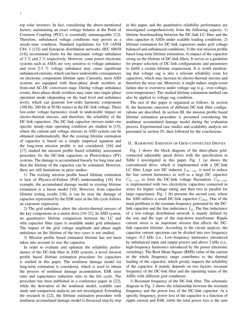
Fig. 1 shows the block diagram of the three-phase grid-connected adjustable speed drives with the specification inTable I investigated in this paper. Fig. 1 (a) shows theconventional drive, which is implemented with a DC-linkLC filter. Large size DC inductor Ldc−cnv is used to reducethe line current harmonics as well as a large DC capacitorCdc−cnv to limit the DC-link voltage fluctuation. Cdc−cnv
is implemented with two electrolytic capacitors connected inseries for higher voltage rating and then two in parallel forlarge capacitance. Fig. 1 (b) presents the second case, wherethe ASD utilizes a small DC-link capacitor Cslim. One of themain problems is the resonant frequency generated by the DC-link capacitor and the line inductance Lg. The line inductanceof a low-voltage distribution network is mainly defined bythe size and the type of the step-down transformer. Ripplecurrent stress is an important stressor that affects the DC-link capacitor lifetime. According to the circuit analysis, thecapacitor current spectrum can be divided into two frequencyranges: 0-2 kHz (i.e., Low-frequency harmonics introducedby unbalanced input and output power) and above 2 kHz (i.e.,high-frequency harmonics introduced by the power electronicswitching). The Root Mean Square (RMS) value of the currentin the whole frequency range contributes to the thermalloading of the capacitor, which greatly impacts the reliabilityof the capacitor. It mainly depends on two factors: resonantfrequency of the DC-link filter and the operating status of theASDs with different grid conditions:
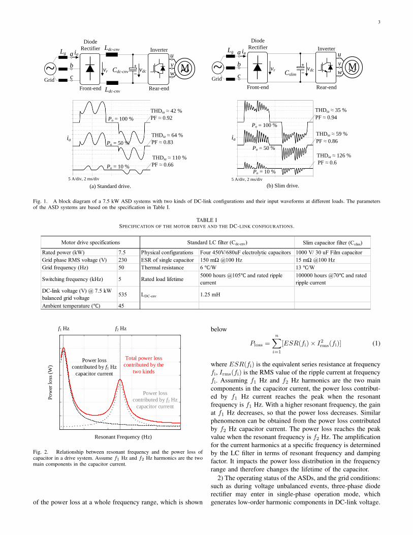
1) Resonant frequency of the DC-link filter. The schematicdiagram in Fig. 2 shows the relationship between the resonantfrequency and the power loss of the DC-link capacitor. At aspecific frequency, power loss of the capacitor is a function ofripple current and ESR, while the total power loss is the sum
3
(a) Standard drive. (b) Slim drive.
Po = 100 %
Po = 50 %
Po = 10 %
5 A/div, 2 ms/div
ia
THDia ≈ 42 %
PF ≈ 0.92
THDia ≈ 64 %
PF ≈ 0.83
THDia ≈ 110 %
PF ≈ 0.66
Po = 100 %
Po = 50 %
Po = 10 %
5 A/div, 2 ms/div
ia
THDia ≈ 35 %
PF ≈ 0.94
THDia ≈ 59 %
PF ≈ 0.86
THDia ≈ 126 %
PF ≈ 0.6
Ldc-cnv
Diode
Rectifier
Cdc-cnv
Grid
Inverter
Rear-end
M
Front-end
~a
b
c
u
v
w
iaLg
vdc+
_vr ~Ldc-cnv
Diode
Rectifier
CslimGrid
Inverter
Rear-end
M
Front-end
~a
b
c
u
v
w
iaLg
vdc+
_vr ~
Fig. 1. A block diagram of a 7.5 kW ASD systems with two kinds of DC-link configurations and their input waveforms at different loads. The parametersof the ASD systems are based on the specification in Table I.
TABLE ISPECIFICATION OF THE MOTOR DRIVE AND THE DC-LINK CONFIGURATIONS.
Slim capacitor filter (Cslim)
Rated power (kW) 7.5 Physical configurations Four 450V/680uF electrolytic capacitors 1000 V/ 30 uF Film capacitor
Grid phase RMS voltage (V) 230 ESR of single capacitor 150 mΩ @100 Hz 15 mΩ @100 Hz
Grid frequency (Hz) 50 Thermal resistance 6 /W 13 /W
Switching frequency (kHz) 5 Rated load lifetime5000 hours @105 and rated ripple
current
100000 hours @70 and rated
ripple current
DC-link voltage (V) @ 7.5 kW
balanced grid voltage535 LDC-cnv 1.25 mH
Ambient temperature () 45
Motor drive specifications Standard LC filter (Cdc-cnv)
Resonant Frequency (Hz)
Po
wer
lo
ss (
W)
Power loss
contributed by f1 Hz
capacitor current
Power loss
contributed by f2 Hz
capacitor current
Total power loss
contributed by the
two kinds
f1 Hz f2 Hz
Fig. 2. Relationship between resonant frequency and the power loss ofcapacitor in a drive system. Assume f1 Hz and f2 Hz harmonics are the twomain components in the capacitor current.
of the power loss at a whole frequency range, which is shown
below
Ploss =
n∑i=1
[ESR(fi)× I2rms(fi)] (1)
where ESR(fi) is the equivalent series resistance at frequencyfi, Irms(fi) is the RMS value of the ripple current at frequencyfi. Assuming f1 Hz and f2 Hz harmonics are the two maincomponents in the capacitor current, the power loss contribut-ed by f1 Hz current reaches the peak when the resonantfrequency is f1 Hz. With a higher resonant frequency, the gainat f1 Hz decreases, so that the power loss decreases. Similarphenomenon can be obtained from the power loss contributedby f2 Hz capacitor current. The power loss reaches the peakvalue when the resonant frequency is f2 Hz. The amplificationfor the current harmonics at a specific frequency is determinedby the LC filter in terms of resonant frequency and dampingfactor. It impacts the power loss distribution in the frequencyrange and therefore changes the lifetime of the capacitor.
2) The operating status of the ASDs, and the grid conditions:such as during voltage unbalanced events, three-phase dioderectifier may enter in single-phase operation mode, whichgenerates low-order harmonic components in DC-link voltage.
4
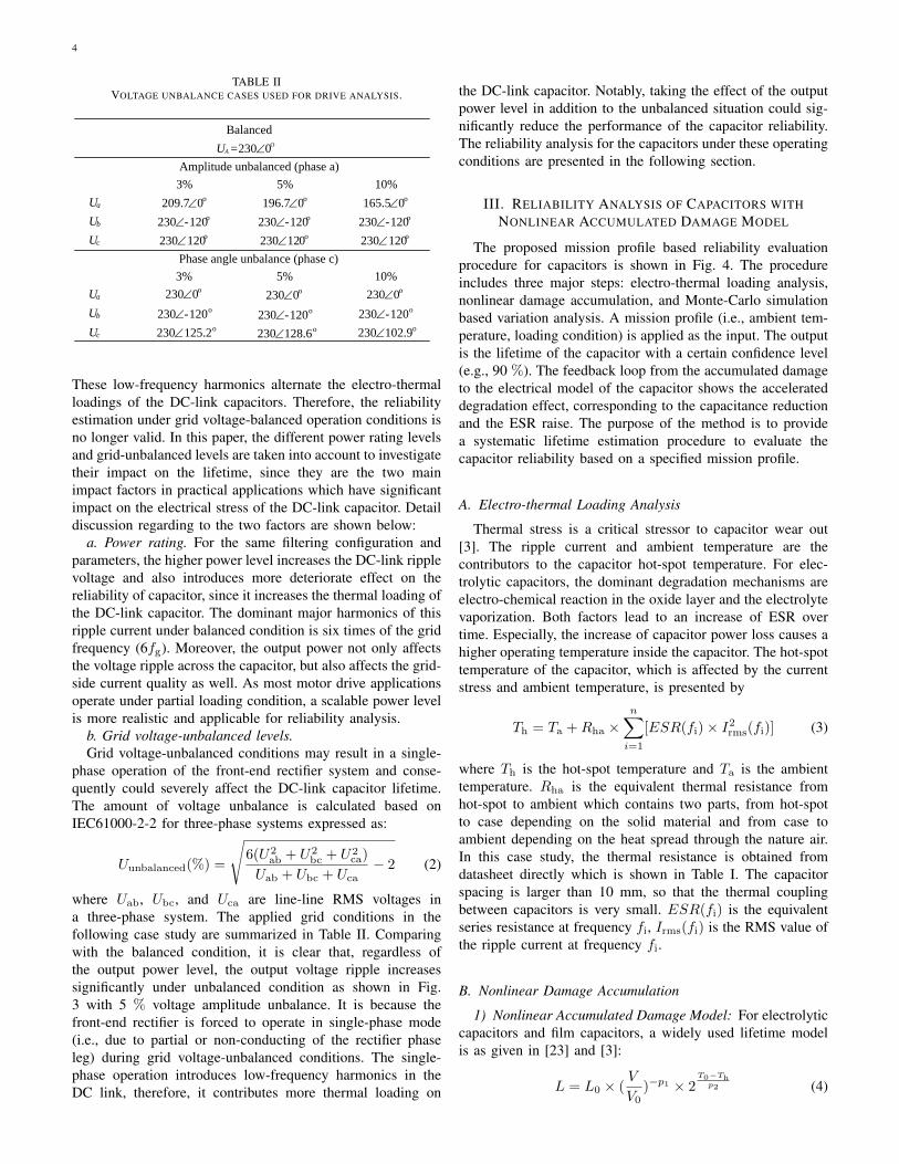
TABLE IIVOLTAGE UNBALANCE CASES USED FOR DRIVE ANALYSIS.
Balanced
UA =2300O
Amplitude unbalanced (phase a)
3% 5% 10%
Ua 209.70o 196.70
o 165.50
o
Ub 230-120o 230-120
o 230-120
o
Uc 230120o 230120
o 230120
o
Phase angle unbalance (phase c)
Ua
3% 5% 10%
Ub
2300o 2300
o 2300
o
Uc
230-120o 230-120
o 230-120
o
230125.2o 230128.6
o 230102.9
o
These low-frequency harmonics alternate the electro-thermalloadings of the DC-link capacitors. Therefore, the reliabilityestimation under grid voltage-balanced operation conditions isno longer valid. In this paper, the different power rating levelsand grid-unbalanced levels are taken into account to investigatetheir impact on the lifetime, since they are the two mainimpact factors in practical applications which have significantimpact on the electrical stress of the DC-link capacitor. Detaildiscussion regarding to the two factors are shown below:
a. Power rating. For the same filtering configuration andparameters, the higher power level increases the DC-link ripplevoltage and also introduces more deteriorate effect on thereliability of capacitor, since it increases the thermal loading ofthe DC-link capacitor. The dominant major harmonics of thisripple current under balanced condition is six times of the gridfrequency (6fg). Moreover, the output power not only affectsthe voltage ripple across the capacitor, but also affects the grid-side current quality as well. As most motor drive applicationsoperate under partial loading condition, a scalable power levelis more realistic and applicable for reliability analysis.
b. Grid voltage-unbalanced levels.Grid voltage-unbalanced conditions may result in a single-
phase operation of the front-end rectifier system and conse-quently could severely affect the DC-link capacitor lifetime.The amount of voltage unbalance is calculated based onIEC61000-2-2 for three-phase systems expressed as:
Uunbalanced(%) =
√6(U2
ab + U2bc + U2
ca)
Uab + Ubc + Uca− 2 (2)
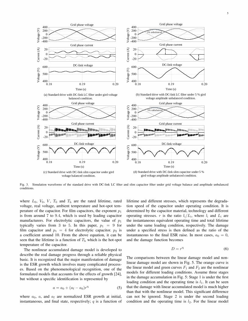
where Uab, Ubc, and Uca are line-line RMS voltages ina three-phase system. The applied grid conditions in thefollowing case study are summarized in Table II. Comparingwith the balanced condition, it is clear that, regardless ofthe output power level, the output voltage ripple increasessignificantly under unbalanced condition as shown in Fig.3 with 5 % voltage amplitude unbalance. It is because thefront-end rectifier is forced to operate in single-phase mode(i.e., due to partial or non-conducting of the rectifier phaseleg) during grid voltage-unbalanced conditions. The single-phase operation introduces low-frequency harmonics in theDC link, therefore, it contributes more thermal loading on
the DC-link capacitor. Notably, taking the effect of the outputpower level in addition to the unbalanced situation could sig-nificantly reduce the performance of the capacitor reliability.The reliability analysis for the capacitors under these operatingconditions are presented in the following section.
III. RELIABILITY ANALYSIS OF CAPACITORS WITHNONLINEAR ACCUMULATED DAMAGE MODEL
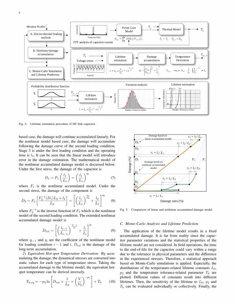
The proposed mission profile based reliability evaluationprocedure for capacitors is shown in Fig. 4. The procedureincludes three major steps: electro-thermal loading analysis,nonlinear damage accumulation, and Monte-Carlo simulationbased variation analysis. A mission profile (i.e., ambient tem-perature, loading condition) is applied as the input. The outputis the lifetime of the capacitor with a certain confidence level(e.g., 90 %). The feedback loop from the accumulated damageto the electrical model of the capacitor shows the accelerateddegradation effect, corresponding to the capacitance reductionand the ESR raise. The purpose of the method is to providea systematic lifetime estimation procedure to evaluate thecapacitor reliability based on a specified mission profile.
A. Electro-thermal Loading Analysis
Thermal stress is a critical stressor to capacitor wear out[3]. The ripple current and ambient temperature are thecontributors to the capacitor hot-spot temperature. For elec-trolytic capacitors, the dominant degradation mechanisms areelectro-chemical reaction in the oxide layer and the electrolytevaporization. Both factors lead to an increase of ESR overtime. Especially, the increase of capacitor power loss causes ahigher operating temperature inside the capacitor. The hot-spottemperature of the capacitor, which is affected by the currentstress and ambient temperature, is presented by
Th = Ta +Rha ×n∑
i=1
[ESR(fi)× I2rms(fi)] (3)
where Th is the hot-spot temperature and Ta is the ambienttemperature. Rha is the equivalent thermal resistance fromhot-spot to ambient which contains two parts, from hot-spotto case depending on the solid material and from case toambient depending on the heat spread through the nature air.In this case study, the thermal resistance is obtained fromdatasheet directly which is shown in Table I. The capacitorspacing is larger than 10 mm, so that the thermal couplingbetween capacitors is very small. ESR(fi) is the equivalentseries resistance at frequency fi, Irms(fi) is the RMS value ofthe ripple current at frequency fi.
B. Nonlinear Damage Accumulation
1) Nonlinear Accumulated Damage Model: For electrolyticcapacitors and film capacitors, a widely used lifetime modelis as given in [23] and [3]:
L = L0 × (V
V0)−p1 × 2
T0−Thp2 (4)
5
(a) Standard drive with DC-link LC filter under gird voltage
balanced condition.
Time (s)
(b) Standard drive with DC-link LC filter under 5 % gird
voltage amplitude unbalanced condition.
Time (s)
(c) Standard drive with DC-link silm capacitor under gird
voltage balanced condition.
Time (s)
(d) Standard drive with DC-link slim capacitor under 5 %
gird voltage amplitude unbalanced condition.
Time (s)
Volt
age (
V)
Curr
ent
(A)
Volt
age (
V)
Volt
age (
V)
Curr
ent
(A)
Volt
age (
V)
Volt
age (
V)
Curr
ent
(A)
Volt
age (
V)
Volt
age (
V)
Curr
ent
(A)
Volt
age (
V)
Grid phase voltage
Grid phase current
DC-link voltage
Grid phase voltage
Grid phase current
DC-link voltage
Grid phase voltage
Grid phase current
DC-link voltage
Grid phase voltage
Grid phase current
DC-link voltage
5% unbalanced
5% unbalanced
Fig. 3. Simulation waveforms of the standard drive with DC-link LC filter and slim capacitor filter under grid voltage balance and amplitude unbalancedconditions.
where L0, V0, V , T0 and Th are the rated lifetime, ratedvoltage, real voltage, ambient temperature and hot-spot tem-perature of the capacitor. For film capacitors, the exponent p1is from around 7 to 9.4, which is used by leading capacitormanufacturers. For electrolytic capacitors, the value of p1typically varies from 3 to 5. In this paper, p1 = 9 forfilm capacitor and p1 = 4 for electrolytic capacitor. p2 isa coefficient around 10. From the above equation, it can beseen that the lifetime is a function of Th which is the hot-spottemperature of the capacitor.
The nonlinear accumulated damage model is developed todescribe the real damage progress through a reliable physicalbasic. It is recognized that the major manifestation of damageis the ESR growth which involves many complicated process-es. Based on the phenomenological recognition, one of theformulated models that accounts for the effects of growth [24],but without a specific identification is represented by
a = a0 + (af − a0)rq (5)
where a0, a, and af are normalized ESR growth at initial,instantaneous, and final state, respectively; q is a function of
lifetime and different stresses, which represents the degrada-tion speed of the capacitor under operating condition. It isdetermined by the capacitor material, technology and differentoperating stresses. r is the ratio li/Li, where li and Li arethe instantaneous equivalent operating time and total lifetimeunder the same loading condition, respectively. The damageunder a specified stress is then defined as the ratio of theinstantaneous to the final ESR raise. In most cases, a0 = 0,and the damage function becomes
D = rq (6)
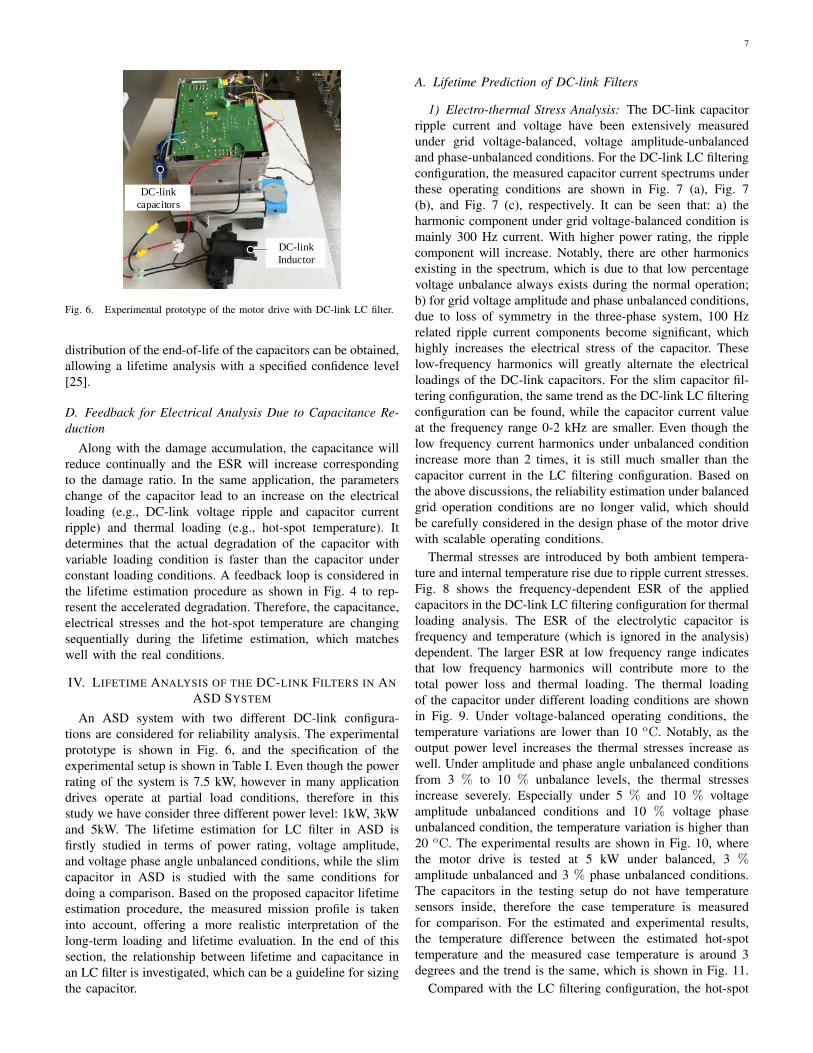
The comparisons between the linear damage model and non-linear damage model are shown in Fig. 5. The orange curve isthe linear model and green curves F1 and F2 are the nonlinearmodels for different loading conditions. Assume three stagesin the damage accumulation in Fig. 5: Stage 1 is under the firstloading condition and the operating time is l1. It can be seenthat the damage with linear accumulated model is much higherthan that with the nonlinear model. This significant differencecan not be ignored. Stage 2 is under the second loadingcondition and the operating time is l2. For the linear model
6
B. Nonlinear damage
accumulation
C. Monte-Carlo Simulation
and Lifetime Prediction
Den
sity
(%
)
Number of hours to failure
L0
n1
Probability distribution functionVariation analysis Lifetime estimation
A. Electro-thermal loading
analysis
Power Loss
Model
2
1
( )I ( )n
loss i rms ii
P ESR f f
Voltage stress
aT
h a loss haT T P R
Thermal Model
hT Lifetime
estimation
Lifetime
estimation
_eq hT
hT
_eq hT
Mission Profile
FFT analysis of capacitor current
0
1 20
0
( ) 2hT T
p pVL L
V
Damage
accumulation
Temperature
Derivation
1
1
1
ii
i
qi i
ni i
l lD
L LV
olta
ge (
V)
Time (s)
0
1 20
0
( ) 2hT T
p pVL L
V
Numbe r of hours to failure
3 %5 %10 %
B1
Cum
ulat
ive
dis
trib
utio
n
Frequency (Hz)
Cu
rren
t (A
)
1
, 2 00 0
1ln
p
h eq totV
T p D TL V
Fig. 4. Lifetime estimation procedure of DC-link capacitor.
based case, the damage will continue accumulated linearly. Forthe nonlinear model based case, the damage will accumulatefollowing the damage curve of the second loading condition.Stage 3 is under the first loading condition and the operatingtime is l3. It can be seen that the linear model will introduceerror in the damage estimation. The mathematical model ofthe nonlinear accumulated damage model is discussed below.Under the first stress, the damage of the capacitor is
D1 = F1
(l1L1
)=
(l1L1
)q1
(7)
where F1 is the nonlinear accumulated model. Under thesecond stress, the damage of the component is
D2 = F2
[F−12 (D1)L2 + l2
L2
]=
[(l1L1
) q1q2
+l2L2
]q2(8)
where F−12 is the inverse function of F2 which is the nonlinear
model of the second loading condition. The extended nonlinearaccumulated damage model is
Dtot =
[(li−1
Li−1
) qi−1qi
+liLi
]qi(9)
where qi−1 and qi are the coefficient of the nonlinear modelfor loading condition i − 1 and i. Dtot is the damage of thelong-term accumulation.
2) Equivalent Hot-spot Temperature Derivation: By accu-mulating the damage, the dynamical stresses are converted intostatic values for each type of temperature stress. Taking theaccumulated damage to the lifetime model, the equivalent hot-spot temperature can be derived inversely.
Th,eq = −p2 ln
[Dtot ×
1
L0×(V
V0
)−p1]+ T0 (10)
Dam
age (
%)
r1 = l1 / L1
Damage ratio (%)
r2 = l2 / L2
r3 = l3 / L3
r1 = l1 / L1
r2 = l2 / L2
r3 = l3 / L3
D1
D2
D3
D1
D2
D3
Damage based on
linear accumulated model
Damage based on
nonlinear accumulated
model
F1F2
Fig. 5. Comparison of linear and nonlinear accumulated damage model.
C. Monte-Carlo Analysis and Lifetime Prediction
The application of the lifetime model results in a fixedaccumulated damage. It is far from reality since the capac-itor parameter variations and the statistical properties of thelifetime model are not considered. In field operations, the timeto the end-of-life for the capacitor could vary within a rangedue to the tolerance in physical parameters and the differencein the experienced stresses. Therefore, a statistical approachbased on Monte-Carlo simulations is applied. Especially, thedistributions of the temperature-related lifetime constants L0,p2 and the temperature tolerance-related parameter Th areplotted. Different values of constants result into differentlifetimes. Then, the sensitivity of the lifetime to L0, p2 andTh can be evaluated individually or collectively. Finally, the
7
DC-link
capacitors
DC-link
Inductor
Fig. 6. Experimental prototype of the motor drive with DC-link LC filter.
distribution of the end-of-life of the capacitors can be obtained,allowing a lifetime analysis with a specified confidence level[25].
D. Feedback for Electrical Analysis Due to Capacitance Re-duction
Along with the damage accumulation, the capacitance willreduce continually and the ESR will increase correspondingto the damage ratio. In the same application, the parameterschange of the capacitor lead to an increase on the electricalloading (e.g., DC-link voltage ripple and capacitor currentripple) and thermal loading (e.g., hot-spot temperature). Itdetermines that the actual degradation of the capacitor withvariable loading condition is faster than the capacitor underconstant loading conditions. A feedback loop is considered inthe lifetime estimation procedure as shown in Fig. 4 to rep-resent the accelerated degradation. Therefore, the capacitance,electrical stresses and the hot-spot temperature are changingsequentially during the lifetime estimation, which matcheswell with the real conditions.
IV. LIFETIME ANALYSIS OF THE DC-LINK FILTERS IN ANASD SYSTEM
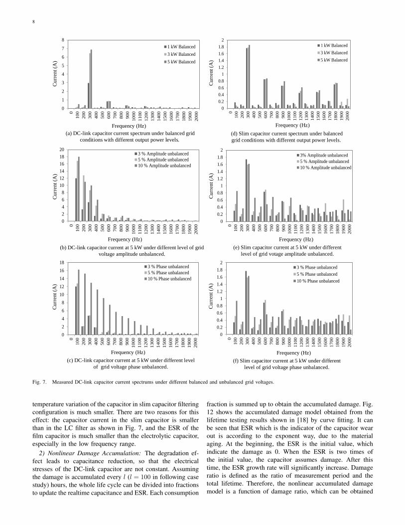
An ASD system with two different DC-link configura-tions are considered for reliability analysis. The experimentalprototype is shown in Fig. 6, and the specification of theexperimental setup is shown in Table I. Even though the powerrating of the system is 7.5 kW, however in many applicationdrives operate at partial load conditions, therefore in thisstudy we have consider three different power level: 1kW, 3kWand 5kW. The lifetime estimation for LC filter in ASD isfirstly studied in terms of power rating, voltage amplitude,and voltage phase angle unbalanced conditions, while the slimcapacitor in ASD is studied with the same conditions fordoing a comparison. Based on the proposed capacitor lifetimeestimation procedure, the measured mission profile is takeninto account, offering a more realistic interpretation of thelong-term loading and lifetime evaluation. In the end of thissection, the relationship between lifetime and capacitance inan LC filter is investigated, which can be a guideline for sizingthe capacitor.
A. Lifetime Prediction of DC-link Filters
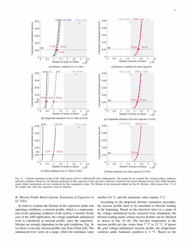
1) Electro-thermal Stress Analysis: The DC-link capacitorripple current and voltage have been extensively measuredunder grid voltage-balanced, voltage amplitude-unbalancedand phase-unbalanced conditions. For the DC-link LC filteringconfiguration, the measured capacitor current spectrums underthese operating conditions are shown in Fig. 7 (a), Fig. 7(b), and Fig. 7 (c), respectively. It can be seen that: a) theharmonic component under grid voltage-balanced condition ismainly 300 Hz current. With higher power rating, the ripplecomponent will increase. Notably, there are other harmonicsexisting in the spectrum, which is due to that low percentagevoltage unbalance always exists during the normal operation;b) for grid voltage amplitude and phase unbalanced conditions,due to loss of symmetry in the three-phase system, 100 Hzrelated ripple current components become significant, whichhighly increases the electrical stress of the capacitor. Theselow-frequency harmonics will greatly alternate the electricalloadings of the DC-link capacitors. For the slim capacitor fil-tering configuration, the same trend as the DC-link LC filteringconfiguration can be found, while the capacitor current valueat the frequency range 0-2 kHz are smaller. Even though thelow frequency current harmonics under unbalanced conditionincrease more than 2 times, it is still much smaller than thecapacitor current in the LC filtering configuration. Based onthe above discussions, the reliability estimation under balancedgrid operation conditions are no longer valid, which shouldbe carefully considered in the design phase of the motor drivewith scalable operating conditions.
Thermal stresses are introduced by both ambient tempera-ture and internal temperature rise due to ripple current stresses.Fig. 8 shows the frequency-dependent ESR of the appliedcapacitors in the DC-link LC filtering configuration for thermalloading analysis. The ESR of the electrolytic capacitor isfrequency and temperature (which is ignored in the analysis)dependent. The larger ESR at low frequency range indicatesthat low frequency harmonics will contribute more to thetotal power loss and thermal loading. The thermal loadingof the capacitor under different loading conditions are shownin Fig. 9. Under voltage-balanced operating conditions, thetemperature variations are lower than 10 oC. Notably, as theoutput power level increases the thermal stresses increase aswell. Under amplitude and phase angle unbalanced conditionsfrom 3 % to 10 % unbalance levels, the thermal stressesincrease severely. Especially under 5 % and 10 % voltageamplitude unbalanced conditions and 10 % voltage phaseunbalanced condition, the temperature variation is higher than20 oC. The experimental results are shown in Fig. 10, wherethe motor drive is tested at 5 kW under balanced, 3 %amplitude unbalanced and 3 % phase unbalanced conditions.The capacitors in the testing setup do not have temperaturesensors inside, therefore the case temperature is measuredfor comparison. For the estimated and experimental results,the temperature difference between the estimated hot-spottemperature and the measured case temperature is around 3degrees and the trend is the same, which is shown in Fig. 11.
Compared with the LC filtering configuration, the hot-spot
8
Cu
rren
t (A
)
Frequency (Hz)
(a) DC-link capacitor current spectrum under balanced grid
conditions with different output power levels.
0
2
4
6
8
10
12
14
16
18
20
0
10
0
20
0
30
0
40
0
50
0
60
0
70
0
80
0
90
0
10
00
11
00
12
00
13
00
14
00
15
00
16
00
17
00
18
00
19
00
20
00
3 % Amplitude unbalanced
5 % Amplitude unbalanced
10 % Amplitude unbalanced
Cu
rren
t (A
)
Frequency (Hz)
0
1
2
3
4
5
6
7
8
0
10
0
20
0
30
0
40
0
50
0
60
0
70
0
80
0
90
0
10
00
11
00
12
00
13
00
14
00
15
00
16
00
17
00
18
00
19
00
20
00
1 kW Balanced
3 kW Balanced
5 kW Balanced
(b) DC-link capacitor current at 5 kW under different level of grid
voltage amplitude unbalanced.
0
2
4
6
8
10
12
14
16
18
0
10
0
20
0
30
0
40
0
50
0
60
0
70
0
80
0
90
0
10
00
11
00
12
00
13
00
14
00
15
00
16
00
17
00
18
00
19
00
20
00
3 % Phase unbalanced
5 % Phase unbalanced
10 % Phase unbalanced
Curr
ent
(A)
Frequency (Hz)
(c) DC-link capacitor current at 5 kW under different level
of grid voltage phase unbalanced.
0
0.2
0.4
0.6
0.8
1
1.2
1.4
1.6
1.8
2
0
10
0
20
0
30
0
40
0
50
0
60
0
70
0
80
0
90
0
10
00
11
00
12
00
13
00
14
00
15
00
16
00
17
00
18
00
19
00
20
00
1 kW Balanced
3 kW Balanced
5 kW Balanced
Frequency (Hz)
(d) Slim capacitor current spectrum under balanced
grid conditions with different output power levels.
0
0.2
0.4
0.6
0.8
1
1.2
1.4
1.6
1.8
2
0
10
0
20
0
30
0
40
0
50
0
60
0
70
0
80
0
90
0
10
00
11
00
12
00
13
00
14
00
15
00
16
00
17
00
18
00
19
00
20
00
3% Amplitude unbalanced
5 % Amplitude unbalanced
10 % Amplitude unbalanced
Frequency (Hz)
(e) Slim capacitor current at 5 kW under different
level of grid votage amplitude unbalanced.
0
0.2
0.4
0.6
0.8
1
1.2
1.4
1.6
1.8
2
0
10
0
20
0
30
0
40
0
50
0
60
0
70
0
80
0
90
0
10
00
11
00
12
00
13
00
14
00
15
00
16
00
17
00
18
00
19
00
20
00
3 % Phase unbalanced
5 % Phase unbalanced
10 % Phase unbalanced
Frequency (Hz)
(f) Slim capacitor current at 5 kW under different
level of grid voltage phase unbalanced.
Curr
ent
(A)
Curr
ent
(A)
Curr
ent
(A)
Fig. 7. Measured DC-link capacitor current spectrums under different balanced and unbalanced grid voltages.
temperature variation of the capacitor in slim capacitor filteringconfiguration is much smaller. There are two reasons for thiseffect: the capacitor current in the slim capacitor is smallerthan in the LC filter as shown in Fig. 7, and the ESR of thefilm capacitor is much smaller than the electrolytic capacitor,especially in the low frequency range.
2) Nonlinear Damage Accumulation: The degradation ef-fect leads to capacitance reduction, so that the electricalstresses of the DC-link capacitor are not constant. Assumingthe damage is accumulated every l (l = 100 in following casestudy) hours, the whole life cycle can be divided into fractionsto update the realtime capacitance and ESR. Each consumption
fraction is summed up to obtain the accumulated damage. Fig.12 shows the accumulated damage model obtained from thelifetime testing results shown in [18] by curve fitting. It canbe seen that ESR which is the indicator of the capacitor wearout is according to the exponent way, due to the materialaging. At the beginning, the ESR is the initial value, whichindicate the damage as 0. When the ESR is two times ofthe initial value, the capacitor assumes damage. After thistime, the ESR growth rate will significantly increase. Damageratio is defined as the ratio of measurement period and thetotal lifetime. Therefore, the nonlinear accumulated damagemodel is a function of damage ratio, which can be obtained

9
Temperature raise
= 8 degree
Temperature raise
= 15 degree
Temperature raise
= 45.7 – 28 = 17.7 degreeTemperature raise
= 18 degree
(a) Drive is tested at 5 kW under
balanced condition.
(b) Drive is tested at 5 kW under 3 % grid
voltage amplitude unbalanced condition.
(c) Drive is tested at 5 kW under 3 % grid voltage
phase unbalanced condition.
Fig. 10. Experimental results of capacitor temperature in LC filtering configuration with 5 kW loading condition.
102
103
104
0
0.5
1
1.5
2
Frequency (Hz)
ES
Rra
tio
( %
)
Datasheet ( 20 °C )
Datasheet ( 40 °C )
Datasheet ( 60 °C )
Datasheet (105 °C )
(a) Relationship between frequency and ESR ratio for 100 Hz of
the electrolytic capacitor with different operating temperatures.
(b) Relationship between frequency and ESR of a film capacitor.
102
103
104
105
0
5
10
15
20
25
Frequency (Hz)
ES
R (
mΩ
)
Fig. 8. Frequency-dependent equivalent series resistance (ESR) of theelectrolytic capacitor B43630 from EPCOS and film capacitors B32776 fromEPCOS.
by curve fitting. Meanwhile, the capacitance is also a functionof the damage ratio. At the beginning, the damage ratio is0, and the capacitance is the initial value. Increasing withthe damage ratio, the capacitance will reduce simultaneously.The relationship between the capacitance reduction and thedamage ratio is shown in Fig. 13, which is used for updatingthe capacitance with different degradation ratios. Therefore,the accelerated degradation of the capacitor can be consideredin the lifetime estimation procedure.
3) Monte-Carlo Based Analysis: This section investigatesthe reliability of DC-link capacitors by taking into account the
0
5
10
15
20
25
30
35
40
BalanceAmplitude
unbalance
Phase
unbalance
Inte
rnal
tem
pera
ture
rais
e (
)
(a) Internal temperature raise of electrolytic capacitor in
LC filter configuration.
1
kW
3
kW
5
kW
3 %
5 %10 %
3 % 5 %
10 %
5 kW
2
2.2
2.4
2.6
2.8
Balance Amplitude
unbalance
Phase
unbalance
(b) Internal temperature raise of film capacitor in
slim capacitor filter configuration.
Inte
rnal
tem
pera
ture
rais
e (
)
1
kW
3
kW
5
kW 3 % 5 %10 %
10 %
5 kW
3 % 5 %
Fig. 9. Internal temperature raise of the capacitors under different loadingcondition.
relevant parameter variations. Two types of uncertainties areconsidered: a) parameter uncertainties in the applied lifetimemodel; b) parameter uncertainties due to manufacturing pro-cess variations among capacitors with the same product partnumber. Regarding the first type of uncertainty, each lifetimemodel has its limitations due to the specific test conditions,component technologies, and failure mechanism considered.Therefore, the uncertainty of fitting coefficients correspondsto the thermal stress p2 is taken into account. Regarding thesecond type of uncertainty, the end-of-life of a large populationof capacitors with the same specification and same product

10
4600 4800 5000 5200 54000
2
4x 10
-3
L0
pd
f
9.5 10 10.50
1
2
p2
pd
f
48 50 52 540
0.2
0.4
Th
pd
f
1.8 2 2.2 2.4x 10
50
10
20
Den
sity
(%
)
Number of hours to failure
1 2 3 4x 10
50
10
20
Den
sity
(%
)
Number of hours to failure
1 2 3 40
10
20
Den
sity
(%
)
Number of hours to failure x 105
Fig. 14. Probability density functions of the parameters under analysis and lifetime probability distribution function.
0
2
4
6
8
10
12
14
16
18
20
Balance 3 % amplitude
unbalance
3 % phase
unbalance
Tem
per
atu
re r
aise
(d
egre
e)
Estimated hot-spot
temperature
Experimentally measured
case temperature
Fig. 11. Comparison between experimental and estimated capacitor temper-ature in LC filtering configuration with 5 kW loading condition.
part number varies in field operations due to variances in themanufacturing process. The variances in L0 and Th are takeninto account in this analysis, since it has a direct effect onthe capacitor lifetime. All the parameters in the analysis aremodeled by means of normal probability distribution functionsas shown in Fig. 14. p2, L0 and Th are assumed to have a 5% variation, respectively, with a 90 % confidence level.
Following the lifetime estimation procedure, the lifetimeof the capacitors in the LC filter are shown in Fig. 15.The study does not consider the varying loading conditionsand grid conditions. Moreover, the lifetime prediction offilm capacitors in the slim drive solution is limited to theelectro-thermal stresses only, while humidity aspect failuremechanisms are not considered for this comparative study.Under the grid voltage-balanced condition, the lifetime of thetwo cases decrease with the increasing output power of thesystem. Compared with the conventional LC filter, the slimcapacitor has longer lifetime under balanced condition. Withthe increase of the grid voltage-unbalanced level, the reliabilitybehavior will change accordingly. For the LC filter, the lifetimemight be significantly shortened, such as the scenarios of 5 %and 10 % amplitude unbalance, and 10 % phase unbalance.The reason is that the low frequency harmonics introduced
0 0.2 0.4 0.6 0.8 1
0
0.2
0.4
0.6
0.8
1
Damage ratio (%)
Dam
age
Damage
Damage line
2.50.9752y x
Fig. 12. Nonlinear accumulated damage model of capacitor.
0 0.2 0.4 0.6 0.8 1
0.85
0.9
0.95
1
Damage ratio (%)
No
rmal
ized
cap
acit
ance
Normalized capacitance
Normalized capacitance line
20.1595 0.00039 1y x x
Fig. 13. The relationship between the capacitance reduction anddamage ratio.
by the unbalance condition are increasing with the unbalancelevel and further amplified by the resonant oscillation, wherethe resonant frequency of the LC filter is around 120 Hz.For the slim capacitor, under amplitude unbalance condition,the lifetime do not decrease with the increasing unbalancelevel. The high frequency harmonics around the resonantfrequency play a critical role compared with the low frequencyharmonics. But because of low ESR at whole frequency range,it has insignificant impact on the power loss, thermal loadingand reliability. This study does not intend to be conclusive to afield application, since the focus of Fig. 15 is to investigate theimpact of loading levels and unbalance levels on the lifetime ofthe DC-link capacitors. Nevertheless, Fig. 15 reveals that thegrid voltage unbalances have obvious impact on the capacitorreliability, which should be taken into account in the designphase of the motor drives.
11
0 0.5 1 1.5 2 2.5 3 3.5
x 105
0
0.01
0.02
0.03
0.04
0.05
Cum
ula
tiv
e d
istr
ibu
tio
n f
un
ctio
n
Number of hours to failure
0 0.5 1 1.5 2 2.5 3 3.5
x 105
0
0.01
0.02
0.03
0.04
0.05
Cum
ula
tiv
e d
istr
ibu
tio
n f
un
ctio
n
Number of hours to failure
0 0.5 1 1.5 2 2.5 3 3.5
x 105
0
0.01
0.02
0.03
0.04
0.05
Cum
ula
tiv
e d
istr
ibu
tio
n f
un
ctio
n
Number of hours to failure
0 0.5 1 1.5 2 2.5 3 3.5
x 105
0
0.01
0.02
0.03
0.04
0.05
Cum
ula
tiv
e d
istr
ibu
tio
n f
un
ctio
n
Number of hours to failure
0 0.5 1 1.5 2 2.5 3 3.5
x 105
0
0.01
0.02
0.03
0.04
0.05
Cum
ula
tiv
e d
istr
ibu
tio
n f
un
ctio
n
Number of hours to failure
0 0.5 1 1.5 2 2.5 3 3.5
x 105
0
0.01
0.02
0.03
0.04
0.05
Cum
ula
tiv
e d
istr
ibu
tio
n f
un
ctio
n
Number of hours to failure
(a) Balance condition for LC filter. (d) Balance condition for slim capacitor.
(b) Amplitude unbalance for LC filter (5 kW). (e) Amplitude unbalance for slim capacitor (5 kW).
(f) Phase unbalance for slim capacitor (5 kW).(c) Phase unbalance for LC filter (5 kW).
1 kW5 kW3 kW
3 %5 %10 %
3 %5 %10 %
>20 yrs area>20 yrs area
>20 yrs area
1 kW3 kW5 kW
3%5 %10 %
3%5 %10 %
>20 yrs area
>20 yrs area
B1
B1
B1B1
B1
B112 yrs
4 yrs 4 yrs 10 yrs
2 yrs 10 yrs
14 yrs 23 yrs 24 yrs
22 yrs 23 yrs
22 yrs
13 yrs
>20 yrs area
Fig. 15. Lifetime estimation results of the ASD system with two different DC-link configurations. The results do not consider the varying loading conditionsand grid conditions. Moreover, the lifetime prediction of film capacitors in the slim drive solution is limited to the electro-thermal stresses only, while humidityaspect failure mechanisms are not considered for this comparative study. The lifetime in the proposed method are the B1 lifetime, which means that 1 % ofthe sample fails when the capacitors reach its lifetime.
B. Mission Profile Based Lifetime Estimation of Capacitor inLC Filter
In order to evaluate the lifetime of the capacitors under realoperating conditions, a mission profile, which is a representa-tion of the operating condition of the system, is needed. In thecase of the ASD application, the voltage amplitude unbalancedlevel is considered as mission profile, since the capacitors’lifetime are strongly dependent on the grid conditions. Fig. 16(a) shows a one-day mission profile case from China [26]. Theunbalanced level varies in a range, where the minimum value
reaches 0.4 %, and the maximum value reaches 3 %.
According to the proposed lifetime estimation procedure,the mission profile need to be translated to thermal loadingat the beginning. Based on the electrical stress in a range ofthe voltage unbalanced levels extracted from simulation, thethermal loading under certain mission profiles can be obtainedas shown in Fig. 16 (b). The hot-spot temperature in themission profile per day varies from 7 oC to 12 oC. If ignorethe grid voltage-unbalanced mission profile, the temperaturevariation under balanced condition is 2 oC. Based on the

12
Volt
age u
nbal
ance
d l
evel
(%)
Dam
age r
ati
o (
%)
Time (hours)
(c) Damage ratio per hour under the mission profile per day.
(a) Voltage unbalance mission profile.
(b) Thermal loading per day under the mission profile.
Time (hours)
0
0.5
1
1.5
2
2.5
3
3.5
1 3 5 7 9 11 13 15 17 19 21 23
Time (hours)
Inte
rnal
tem
pera
ture
rais
e (D
egre
e)
0
2
4
6
8
10
12
14
1 3 5 7 9 11 13 15 17 19 21 23
0
0.0001
0.0002
0.0003
0.0004
0.0005
0.0006
0.0007
0.0008
1 3 5 7 9 11 13 15 17 19 21 23
Fig. 16. Mission profile and damage ratio of capacitor per day.
estimated thermal loading and the nonlinear accumulateddamage model discussed in above section, the damage forone day can be accumulated, which is shown in Fig. 16 (c).Because of the data availability, the mission profile per dayshown in Fig. 16 (a) is extended to the whole year to estimatethe B1 lifetime. Fig. 17 shows the lifetime estimation resultswith the voltage unbalanced mission profile. The B1 lifetimeof the mission profile based estimation is one year shorter thanthat the lifetime with the grid voltage balanced condition. Itindicates the mission profile introduces a significant differencein the lifetime and can not be ignored during the lifetimeestimation procedure when doing design.
C. Capacitor Sizing Considering Reliability Performance
The conventional LC filter sizing criteria provide a capac-itance range based on the stability analysis, while it does
0 0.5 1 1.5 2 2.5 3 3.5
x 105
0
0.01
0.02
0.03
0.04
0.05
Cum
ula
tive d
istr
ibuti
on
functi
on
Number of hours to failure
B1 13 yrs 14 yrs
>20 yrs area
Fig. 17. Lifetime comparison of a 5 kW ASD under grid voltage balancedcondition (black curve) and grid voltage unbalanced mission profile (reddashed curve).
50
100
150
200
250
300
350
100 500 900
Capacitance (µF)
Res
on
ant
freq
uen
cy (
Hz)
350 µF, fresonant= 165 Hz
150 µF, fresonant= 258 Hz
680 µF, fresonant= 121 Hz
Fig. 18. Relationship between capacitance and resonant frequency of theDC-link LC filter using the parameters in Table I.
not consider reliability into the sizing procedure. This sectionstudies the lifetime variation due to different capacitance. Therange of capacitance results in different DC-link capacitorcurrent spectrum, which will further change the lifetime of theDC-link capacitor. If the inductance is constant, the resonantfrequency of the LC filter is changed with the capacitance. Fora case study, the motor drive with the same series componentsshown in Table I and range of capacitance is investigated. Therelationship between capacitance and the resonant frequencyis shown in Fig. 18. In the conventional LC filter sizingprocedure, the resonant frequency of the LC filter is alwaysdesigned below 300 Hz to filter the six times fundamentalripple component. From the resonant frequency perspective,larger capacitance values move the resonant frequency awayfrom 300 Hz, which will reduce the gain for the 300 Hz rippleand it has the potential to reduce the thermal loading.
The lifetime estimation procedure proposed in this paper isapplied. The current spectrum with different capacitance canbe obtained through a mathematical model, circuit simulationor experimental measurement. The data incorporated in thefollowing analysis are based on simulation in Matlab R2014a.

13
100 500 9000
Capacitance (µF)
20
40
60
Inte
rnal
tem
pera
ture
rais
e (
)
Fig. 19. Estimated internal temperature raise of the capacitor with differentcapacitance under balanced condition.
0
2
4
6
8
10
12x 10
4
B1
lif
etim
e (h
ou
rs)
100 500 900
Capacitance (µF)
10 years
Fig. 20. Estimated lifetimes of DC-link capacitor with different capacitancesunder balanced grid voltages.
The estimated hot-spot temperature can be seen in Fig. 19 andshows that with larger capacitance, the hot-spot temperature isreduced due to a) smaller gain for the 300 Hz ripple current,and b) larger value capacitor has smaller ESR. The estimatedlifetime can be seen in Fig. 20. The lifetime will increasewith the capacitance, which follows the opposite trend to thetemperature. If it is assumed that 10 years is the design targetunder balanced conditions, the capacitance should be sizedlarger than 300 µF from the reliability point of view.
From Fig. 15, it can be seen that the lifetime of theDC-link capacitor under unbalanced conditions has differentperformance compared with balanced condition, and the worstcase in this study is in 5 kW drive under 10 % phase angleunbalance condition. Therefore, the case study correspondingto the impact of the capacitance is based on the worst case.Following the same evaluation procedure with the balancedcondition, the hot-spot temperature of the capacitors under10 % phase angle unbalanced condition can be estimated,which can be seen in Fig. 21. The relationship betweencapacitance and estimated hot-spot temperature is not linearas the case study with balanced condition in Fig. 19. It not
100 500 9000
20
Capacitance (µF)
Inte
rnal
tem
pera
ture
rais
e (
)
350 µF, fresonant= 165 Hz
150 µF,
fresonant= 258 Hz
650 µF, fresonant= 124 Hz
680 µF, fresonant= 121 Hz40
60
Fig. 21. Estimated Th of the capacitor with different capacitance under 10% phase angle unbalanced condition.
0
2
4
6
8
10
12x 10
4
B1 l
ifet
ime
(hours
)
100 500 900
Capacitance (µF)
150 µF,
fresonant= 258 Hz
350 µF,
fresonant= 165 Hz
650 µF, fresonant= 124 Hz
680 µF, fresonant= 121 Hz
Fig. 22. Estimated lifetimes of the DC-link capacitor with differentcapacitances under 10 % phase angle unbalance condition.
only depends on the gain of the harmonics, but it is alsorelated to the nonlinear current distribution. Fig. 22 showsthe estimated lifetime of the DC-link capacitors with range ofcapacitance. With larger capacitance, the resonant frequencywill move to lower frequency range and get closer to theharmonic frequency. When the resonant frequency is aroundthe harmonic frequency, the shortest lifetime can be foundwhere the capacitance is 350 µF . With further larger capaci-tance value, the resonant frequency becomes even smaller andconsequently reduces the gain at the harmonic frequency aswell as the thermal loading of the DC-link capacitor. Based onthe above estimated lifetime, it can be seen that the capacitanceshould be selected larger than 350 µF in order to reach thelifetime target for both balanced and unbalanced conditions.
V. CONCLUSIONS
This paper investigates the reliability of the DC-link capac-itors in grid-connected adjustable speed drives. A capacitorlifetime estimation procedure considering the nonlinear accu-mulated damage model for long-term and variable loadingconditions is proposed. Based on the proposed estimation
14
method, the lifetime of the DC-link capacitor in a LC filterand a comparable slim capacitor DC-link filter under gridvoltage balanced and unbalanced conditions are investigated.It quantifies that significant impact of power rating and gridconditions, which should be considered in the concept phaseand design phase of a motor drive development. Based on thecase study with the presented specification, it can be concludedthat:
1) The lifetime of the LC filter DC-link configurationis lower than half of the slim capacitor, especially underamplitude and phase unbalance conditions;
2) In normal operation, the existing grid voltage-unbalancedconditions reduce the lifetime of the capacitor around 1 year.Due to the unbalanced condition existed all the time, thelong-term mission profile based lifetime estimation is morecompatible with the real situation.
3) From the reliability point of view, the capacitor in theDC-link LC filtering configuration of the motor drive shouldbe larger than 350 µF in order to keep lifetime longer than 10years in the studied case.
REFERENCES
[1] F. Zare, H. Soltani, D. Kumar, P. Davari, H. A. M. Delpino,and F. Blaabjerg, “Harmonic emissions of three-phase dioderectifiers in distribution networks,” IEEE Access, vol. 5, pp.2819–2833, 2017.
[2] M. Hinkkanen and J. Luomi, “Induction motor drives equippedwith diode rectifier and small dc-link capacitance,” IEEE Trans.Ind. Electron., vol. 55, no. 1, pp. 312–320, Jan. 2008.
[3] H. Wang and F. Blaabjerg, “Reliability of capacitors for dc-linkapplications in power electronic converters-an overview,” IEEETrans. Ind. Appl., vol. 50, no. 5, pp. 3569–3578, Sep. 2014.
[4] H. Wen, W. Xiao, X. Wen, and P. Armstrong, “Analysis andevaluation of dc-link capacitors for high-power-density electricvehicle drive systems,” IEEE Trans. Vehicular Tech., vol. 61,no. 7, pp. 2950–2964, Sep. 2012.
[5] K. S. Rajashekara, V. Rajagopalan, A. Sevigny, and J. Vithay-athil, “Dc link filter design considerations in three-phase voltagesource inverter-fed induction motor drive system,” IEEE Trans.Ind. Appl., vol. 23, no. 4, pp. 673–680, Jul. 1987.
[6] B. Sun, X. Fan, C. Qian, and G. Zhang, “Pof-simulation-assistedreliability prediction for electrolytic capacitor in led drivers,”IEEE Trans. Ind. Electron., vol. 63, no. 11, pp. 6726–6735,Nov. 2016.
[7] VISHAY, General Technical Information.[8] M. Hinkkanen and J. Luomi, “Induction motor drives equipped
with diode rectifier and small dc-link capacitance,” IEEE Trans.Ind. Electron., vol. 55, no. 1, pp. 312–320, Jan. 2008.
[9] Council of European Energy Regulators (CEER), 5th CeerBenchmarking Report on the Quality of Electricity Supply,2011.
[10] S. Elphick, P. Ciufo, G. Drury, V. Smith, S. Perera, andV. Gosbell, “Large scale proactive power-quality monitoring:An example from australia,” IEEE Trans. Power Del., vol. 32,no. 2, pp. 881–889, Apr. 2017.
[11] A. V. Jouanne and B. Banerjee, “Assessment of voltage unbal-ance,” IEEE Trans. Power Del., vol. 16, no. 4, pp. 782–790,Apr. 2001.
[12] E. P. E. A. Center, “Input performance of asds during supplyvoltage unbalance,” Power Quality Testing Network PQTNBrief, no. 28, 1996.
[13] ANSI C84. 1: American National Standard for electric powersystems and equipment-voltage ratings (60 Hertz), 2006.
[14] IEC 60038: IEC standard voltages, 2002.
[15] K. Lee, T. M. Jahns, G. Venkataramanan, and W. E. Berkopec,“Dc-bus electrolytic capacitor stress in adjustable-speed drivesunder input voltage unbalance and sag conditions,” IEEE Trans.Ind. Appl., vol. 43, no. 2, pp. 495–504, Mar. 2007.
[16] Y. Yang, K. Ma, H. Wang, and F. Blaabjerg, “Instantaneous ther-mal modeling of the dc-link capacitor in photovoltaic systems,”in Proc. IEEE APEC, Mar. 2015, pp. 2733–2739.
[17] ——, “Mission profile translation to capacitor stresses in grid-connected photovoltaic systems,” in Proc. IEEE ECCE, Sep.2014, pp. 5479–5486.
[18] D. Zhou, H. Wang, and F. Blaabjerg, “Mission profile basedsystem-level reliability analysis of dc/dc converters for a backuppower application,” IEEE Trans. on Power Electron., pp. 1–1,2017.
[19] D. Kumar, P. Davari, F. Zare, and F. Blaabjerg, “Analysis ofthree-phase rectifier systems with controlled dc-link currentunder unbalanced grids,” in Proc. IEEE APEC, Mar. 2017, pp.2179–2186.
[20] X. Pei, W. Zhou, and Y. Kang, “Analysis and calculation ofdc-link current and voltage ripples for three-phase inverter withunbalanced load,” IEEE Trans. Power Electron., vol. 30, no. 10,pp. 5401–5412, Oct. 2015.
[21] H. Wang, P. Davari, D. Kumar, F. Zare, and F. Blaabjerg, “Theimpact of grid unbalances on the reliability of dc-link capacitorsin a motor drive,” in Proc. IEEE ECCE, Oct. 2017, pp. 4345–4350.
[22] H. Wang, P. Davari, H. Wang, D. Kumar, F. Zare, and F. Blaab-jerg, “Lifetime benchmarking of two dc-link passive filteringconfigurations in adjustable speed drives,” in Proc. IEEE APEC,Mar. 2018, pp. 1–1.
[23] S. G. Parler, “Deriving lifet multipliers for electrolytic capac-itors,” in IEEE Power Electronics Society Newsletter, vol. 16,no. 1, Feb. 2004, pp. 11–12.
[24] A. Fatemi and L. Yang, “Cumulative fatigue damage and lifeprediction theories: a survey of the state of the art for homoge-neous materials,” International journal of fatigue, vol. 20, no. 1,pp. 9–34, 1998.
[25] P. D. Reigosa, H. Wang, Y. Yang, and F. Blaabjerg, “Predictionof bond wire fatigue of igbts in a pv inverter under a long-termoperation,” IEEE Trans. Power Electron., vol. 31, no. 10, pp.7171–7182, Oct. 2016.
[26] http://www.gzweix.com/article/sort0662/sort0664/info-305423.html.
Haoran Wang (S’15) received the B.S. and M.S.degrees in control science and engineering fromWuhan University of Technology, Wuhan, China,in 2012 and 2015, respectively. He is currently anPhD fellow in Center of Reliable Power Electronics(CORPE), Aalborg University, Aalborg, Denmark.
From 2013 to 2014, he was research assistant withthe Department of Electrical Engineering, TsinghuaUniversity, Beijing, China. He was a Visiting Sci-entist with the ETH Zurich, Switzerland, from 2017to 2018. His research interests include reliability of
capacitors and multi-objective life-cycle performance optimization of powerelectronic systems.

15
Pooya Davari (S’11-M’13) received the B.Sc. andM.Sc. degrees in electronic engineering from theUniversity of Mazandaran, Babolsar, Iran, in 2004and 2008, respectively, and the Ph.D. degree inpower electronics from Queensland University ofTechnology (QUT), Brisbane, Australia, in 2013.From 2005 to 2010, he was involved in severalelectronics and power electronics projects as a De-velopment Engineer. From 2010 to 2014, he investi-gated and developed high-power high-voltage pow-er electronic systems for multidisciplinary projects,
such as ultrasound application, exhaust gas emission reduction, and tissue-materials sterilization. From 2013 to 2014, he was a Lecturer with QUT. Hejoined, as a Postdoctoral Researcher, the Department of Energy Technology,Aalborg University, Aalborg, Denmark, in 2014, where he is currently anAssociate Professor. His current research interests include EMI/EMC inpower electronics, WBG-based power converters, active front-end rectifiers,harmonic mitigation in adjustable-speed drives, and pulsed power applications.Dr. Davari received a research grant from the Danish Council of IndependentResearch (DFF-FTP) in 2016.
Huai Wang (M’12-SM’17) received the B.E. degreein electrical engineering, from Huazhong Universityof Science and Technology, Wuhan, China, in 2007and the Ph.D. degree in power electronics, fromthe City University of Hong Kong, Hong Kong,in 2012. He is currently an Associate Professor atthe Center of Reliable Power Electronics (CORPE),Aalborg University, Aalborg, Denmark. He was aVisiting Scientist with the ETH Zurich, Switzerland,from Aug. to Sep. 2014, and with the MassachusettsInstitute of Technology (MIT), USA, from Sep. to
Nov. 2013. He was with the ABB Corporate Research Center, Switzerland,in 2009. His research addresses the fundamental challenges in modelling andvalidation of power electronic component failure mechanisms, and applicationissues in system-level predictability, condition monitoring, circuit architecture,and robustness design. Dr. Wang received the Richard M. Bass OutstandingYoung Power Electronics Engineer Award from the IEEE Power ElectronicsSociety in 2016, and the Green Talents Award from the German FederalMinistry of Education and Research in 2014. He is currently the AwardChair of the Technical Committee of the High Performance and EmergingTechnologies, IEEE Power Electronics Society, and the Chair of IEEEPELS/IAS/IE Chapter in Denmark. He serves as an Associate Editor of IETPOWER ELECTRONICS, IEEE JOURNAL OF EMERGING AND SELECT-ED TOPICS IN POWER ELECTRONICS, and IEEE TRANSACTIONS ONPOWER ELECTRONICS.
Dinesh Kumar (S’08-M’12) received Master ofTechnology (M. Tech) in power system engineeringfrom Indian Institute of Technology (IIT), Roorkee,India, in 2004, and Ph.D. degree in power electronicsfrom the University of Nottingham, U.K., in 2010.From 2004-2005, he served as a Lecturer in Electri-cal Engineering Department at National Institute ofTechnology, Kurukshetra, India. In 2006, he joinedTechnical University Chemnitz, Germany as a Re-search Fellow. From 2006 to 2010, he investigatedand developed matrix converter based multidrive
system for aerospace applications. Since 2011, he has been with the DanfossDrives A/S, Denmark, where he is involved in many research and industrialprojects. His current research interests include motor drive, harmonic analysisand mitigation techniques, power quality and electromagnetic interference inpower electronics. He is the Editor of International Journal of Power Electron-ics and the Associate Editor of IEEE Transaction on Industry Applications.
Firuz Zare (S’98-M’01-SM’06) received his PhDin Power Electronics from Queensland Universityof Technology in Australia in 2002. He has spentseveral years in industry as a team leader working onpower electronics and power quality projects. Prof.Zare has received several awards such as an Aus-tralian Future Fellowship, Symposium Fellowship bythe Australian Academy of Technological Science,early career academic excellence research awardand John Madsen Medal from Engineers Australia.He has published over 220 journal and conference
papers and technical reports in the area of Power Electronics. He is anacademic staff at the University of Queensland in Australia and a Task ForceLeader of Active Infeed Converters within Working Group one at the IECstandardization TC77A. Prof Zare is a senior member of IEEE, the Editor inChief of International Journal of Power Electronics and the associate editorof IEEE Access journal. His main research areas are a) Power ElectronicsTopology, Control and Applications, b) Power Quality and Regulations andc) Pulsed Power Applications.
Frede Blaabjerg (S’86-M’88-SM’97-F’03) waswith ABB-Scandia, Randers, Denmark, from 1987to 1988. From 1988 to 1992, he got the PhD degreein Electrical Engineering at Aalborg University in1995. He became an Assistant Professor in 1992,an Associate Professor in 1996, and a Full Profes-sor of power electronics and drives in 1998. From2017 he became a Villum Investigator. His currentresearch interests include power electronics and itsapplications such as in wind turbines, PV systems,reliability, harmonics and adjustable speed drives.
He has published more than 500 journal papers in the fields of powerelectronics and its applications. He is the co-author of two monographs andeditor of 7 books in power electronics and its applications. He has received24 IEEE Prize Paper Awards, the IEEE PELS Distinguished Service Award in2009, the EPE-PEMC Council Award in 2010, the IEEE William E. NewellPower Electronics Award 2014 and the Villum Kann Rasmussen ResearchAward 2014. He was the Editor-in-Chief of the IEEE TRANSACTIONS ONPOWER ELECTRONICS from 2006 to 2012. He has been DistinguishedLecturer for the IEEE Power Electronics Society from 2005 to 2007 and forthe IEEE Industry Applications Society from 2010 to 2011 as well as 2017 to2018. In 2018 he is President Elect of IEEE Power Electronics Society. He isnominated in 2014, 2015, 2016 and 2017 by Thomson Reuters to be betweenthe most 250 cited researchers in Engineering in the world. In 2017 he becameHonoris Causa at University Politehnica Timisoara (UPT), Romania.