Embed Size (px)
Citation preview
Aalborg Universitet
Investigation into the Control Methods to Reduce the DC-Link Capacitor Ripple Currentin a Back-to-Back Converter
Qin, Zian; Wang, Huai; Blaabjerg, Frede; Loh, Poh Chiang
Published in:Proceedings of the 2014 IEEE Energy Conversion Congress and Exposition (ECCE)
DOI (link to publication from Publisher):10.1109/ECCE.2014.6953395
Publication date:2014
Document VersionEarly version, also known as pre-print
Link to publication from Aalborg University
Citation for published version (APA):Qin, Z., Wang, H., Blaabjerg, F., & Loh, P. C. (2014). Investigation into the Control Methods to Reduce the DC-Link Capacitor Ripple Current in a Back-to-Back Converter. In Proceedings of the 2014 IEEE Energy ConversionCongress and Exposition (ECCE) (pp. 203-210). IEEE Press. https://doi.org/10.1109/ECCE.2014.6953395
General rightsCopyright and moral rights for the publications made accessible in the public portal are retained by the authors and/or other copyright ownersand it is a condition of accessing publications that users recognise and abide by the legal requirements associated with these rights.
- Users may download and print one copy of any publication from the public portal for the purpose of private study or research. - You may not further distribute the material or use it for any profit-making activity or commercial gain - You may freely distribute the URL identifying the publication in the public portal -
Take down policyIf you believe that this document breaches copyright please contact us at [email protected] providing details, and we will remove access tothe work immediately and investigate your claim.

© 2014 IEEE. Personal use of this material is permitted. Permission from IEEE must be obtained for all other uses, in any current or future media, including reprinting/republishing this material for advertising or promotional purposes, creating new collective works, for resale or redistribution to servers or lists, or reuse of any copyrighted component of this work in other works. Digital Object Identifier (DOI): Proceedings of the IEEE Energy Conversion Congress and Exposition (ECCE 2014), Pittsburgh, PA, USA, 14-18 September, 2014.
Investigation into the Control Methods to Reduce the DC-Link Capacitor Ripple Current in a Back-to-Back Converter Zian Qin Huai Wang Frede Blaabjerg Poh Chiang Loh Suggested Citation
Z. Qin, H. Wang, F. Blaabjerg, and P. C. Loh, “Investigation into the control methods to reduce the DC-link capacitor ripple current in a back-to-back converter," in Proc. IEEE Energy Convers. Congr. and Expo., 2014, pp. 203-210.
Investigation into the Control Methods to Reduce theDC-Link Capacitor Ripple Current in a
Back-to-Back Converter
Zian Qin, Huai Wang, Member, IEEE, Frede Blaabjerg, Fellow, IEEE, Poh Chiang Loh, Senior Member, IEEEDepartment of Energy Technology, Aalborg University
9220 Aalborg, [email protected], [email protected], [email protected], [email protected]
Abstract—Three-phase back-to-back converters have a widerange of applications (e.g. wind turbines) in which the reliabilityand cost-effectiveness are of great concern. Among other com-ponents and interconnections, DC-link capacitors are one of theweak links influenced by environmental stresses (e.g. ambienttemperature, humidity, etc.) and operating stresses (e.g. voltage,ripple current). This paper serves to investigate the ways ofreducing ripple current stresses of DC-link capacitors in back-to-back converters. The outcome could benefit to achieve either anextended lifetime for a designed DC-link or a reduced DC-linksize for fulfilling a specified lifetime target. The proposed controlstrategies have been demonstrated on a study case of a 1.5 kWconverter prototype. The experimental verifications are in wellagreement with the theoretical analyses.
I. INTRODUCTION
It has been observed in recent years that the challengesin power electronics design is in a way of more demandingreliability performance and more stringent cost constraint[1–3], such as the pressure of cost-of-energy reduction inrenewable energies. Three-phase voltage-source Back-to-Back(BTB) converters are widely used in wind turbines, of whichthe DC-link capacitors are found to be one of the weaklinks in field operations. Both aluminum electrolytic capacitorsand film capacitors have been designed into different windturbine products. For aluminum electrolytic capacitors, theambient temperature and the internal temperature rise dueto ripple current are of critical stressors that influence thelifetime. For film capacitors, the reliability performance isstill of a high level of uncertainty in field operation due torelatively lack of field experiences. In high ripple current stressscenarios, high internal temperature raises could still occur.Moreover, the internal temperature variations will induce morechance of moisture absorption, which is a critical stressorto the failure of film capacitors [4]. The capacitor lifetimedependence on temperature and voltage has been discussedin [4] and is represented in (1), where L is the lifetime,V is maximum voltage across capacitors, KB is Boltzmannsconstant (8.62× 10⁻⁵ eV/K), Ea is activation energy, n is thevoltage stress exponent, T is the hotspot temperature, Tambis the ambient temperature, Rha is the equivalent thermalresistance from hotspot to ambient, ESR(fi) is the equivalentseries resistance at frequency fi, Irms(fi) is the root-mean-square value of the ripple current at frequency fi. It canbe noted that the ripple current spectrum contributes to the
hotspot temperature in terms of self-heating of the capacitors.Therefore, the reduction of ripple current stresses will bebeneficial to improve the reliability or to reduce the size ofDC links composed of either electrolytic capacitors or filmcapacitors, or both.
L ∝ V −n × exp(
EaKBT
)T = Tamb +Rha ×
n∑i=1
ESR(fi)× I2rms(fi)(1)
Efforts have been devoted to the reduction of ripple currentstresses of capacitors in three-phase systems in the prior-artresearch [5–8]. Current source converters are used for the windpower system in order to avoid the DC link capacitor [5].However the performance is not as good as voltage sourceconverters in terms of the power loss caused by the DC linkinductor and the quality of the current especially at low powerratio. The voltage source converter technology is much moremature and it is still the dominant in the market as well asin the research. The feed forward control and direct capacitorcurrent control can be used to reduce the imbalance betweenthe input and output power of the DC link capacitor duringthe dynamic process [6], [8]. However, the approaches cannothandle the ripple current with a carrier frequency on the DClink, which is introduced by the PWM modulation and existsduring both the dynamic and steady state.
The research focusing on the carrier frequency ripple cur-rent has therefore be conducted [9–15]. The RMS value of theDC capacitor current is derived for a AC-DC-AC system witha diode rectifier in front [9]. The analytical result has a goodaccuracy even the ac currents contain high ripples. Howeverthe spectrum of the DC link current is a more critical factor forthe DC link capacitor due to its frequency-dependent ESR(fi)[16]. The spectrum of the DC link current in PWM convertershas been derived for a single leg and three-phase systems,respectively [10], [11], [12], which actually contains DC com-ponent, baseband harmonics, carrier frequency harmonics, andcarrier-sideband harmonics. However, only the DC capacitorcurrent in a single stage power converter is analyzed, whilethat in a BTB converter is still unknown. Another importantaspect is the approaches to reduce the DC capacitor current.Synchronizing the carriers of the back-to-back converter is anefficient way to reduce the DC-link current, where the in-phasecondition is found to be the most optimal [7]. However, more
978-1-4799-5776-7/14/$31.00 ©2014 IEEE
inverterrectifier
FilterAC
source
ia1
ib1
ic1
FilterAC
load
capi
2dci1dci
ia2
ib2
ic2
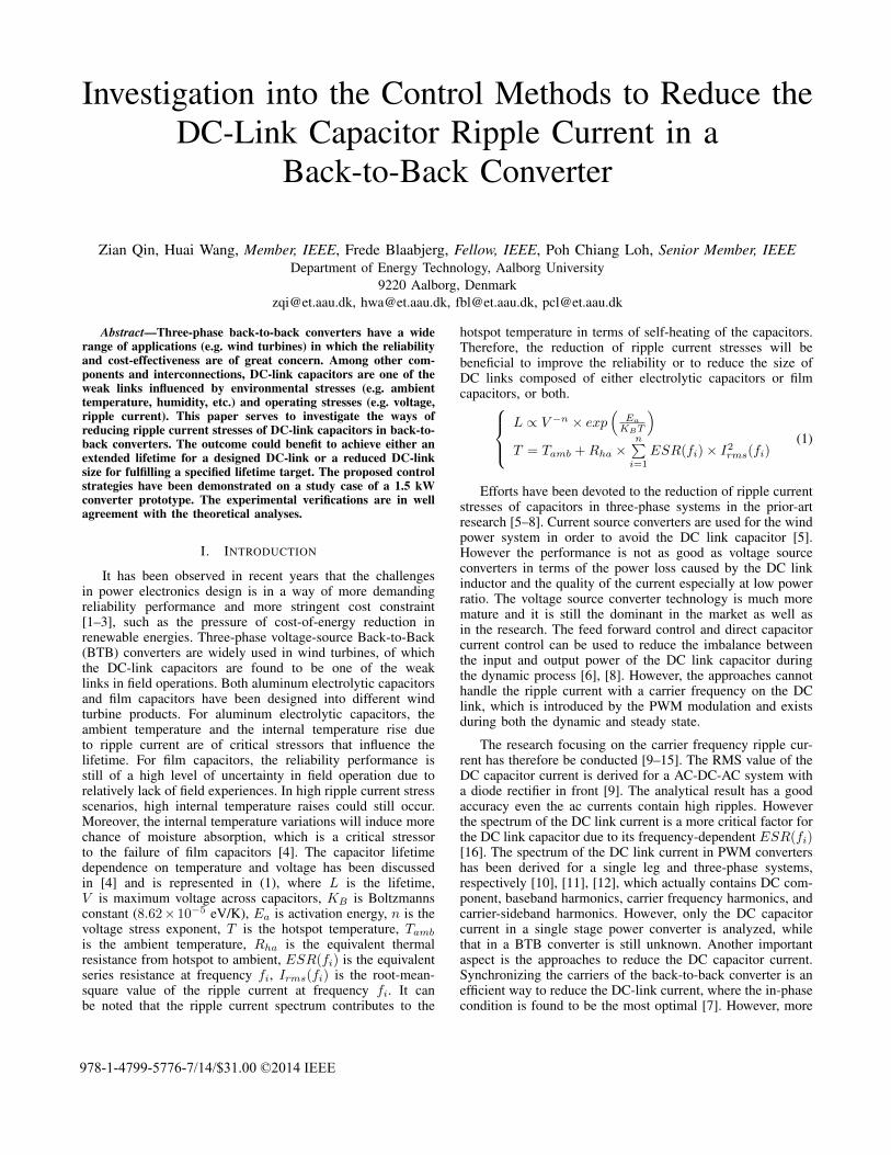
Fig. 1. Scheme of the back-to-back converter.
details are still missing, and the impact of the other parametersis also worthy to be studied.
Therefore, in this paper the impact of the parameters on theDC link current as well as the DC capacitor current is inves-tigated based on a simple derivation. Then the opportunitiesof using control strategies to reduce the DC capacitor currentcan be created. The analytical results are finally verified bythe simulation results and the test on a 1.5 kW prototype inthe laboratory.
II. ANALYSIS OF THE DC LINK CURRENT
Fig. 1 demonstrates the scheme of a BTB converter, whichis composed of a three-phase rectifier and a three-phaseinverter. iax, ibx, and icx are the AC currents, idcx is theDC link current, icap is the current of the DC link capacitor(x = 1 or 2, which represents the rectifier and the inverter,respectively). According to the Kirchhoff’s Current Law, icapis the difference between idc1 and idc2. It is therefore essentialfirst to analyze the generation mechanism of idcx. In fact, asin a voltage source converter (the rectifier or the inverter), theidcx is the combination of iax, ibx and icx. The switchingbetween the AC currents finally leads to the pulsed idcx. Aspectrum analysis is thus carried out for idcx in a universalthree-phase voltage converter. The DC link current is illustratedin Fig. 2, where the Refa, Refb and Refc are the referencesof the modulation, ia, ib and ic are the ac currents, which areexpressed as follows,
Refa = Mcos[ω0(t− t0)] +M3rd
Refb = Mcos[ω0(t− t0)− 2π3 ] +M3rd
Refc = Mcos[ω0(t− t0) + 2π3 ] +M3rd
(2)
ia = Icos[ω0(t− t0) + ϕ]ib = Icos[ω0(t− t0)− 2π
3 + ϕ]ic = Icos[ω0(t− t0) + 2π
3 + ϕ](3)
where M is the modulation index, ω0 is the fundamentalfrequency, M3rd is the third-harmonic injection, I is theamplitude of the ac currents, ϕ is the power factor angle of theac side, t0 is the initial time, which is indicated in Fig. 2. It canbe seen that, the dc link current has the same envelope withthe ac currents. Moreover, according to the cross points of thereferences, a fundamental cycle is divided into six segments.In each segment the dc link current is composed of two ac
ai bici
ia,-ib ia,-ic ib,-ic ib,-ia ic,-ia
5 ms
ic,-ib
0
1
-1
0
Refa Refb Refc
Refa
Refb
Refc
dci
t0
I II III IV VVI
Fig. 2. Illustration of the converter side dc current.
currents, which are respectively the positive and minus currentsin the phase of the top and bottom references. For example,in Segment I since Refa and Refb are the top and bottomreferences, the dc link current idc is composed of ia and ib. Inthe zoomed figure, it is found that the dc link current is actuallycomposed of four pulses in each switching cycle, where theamplitude is that of the corresponding ac current as mentionedabove, while the durations of the current pulses are determinedby the difference between the references. It should be notedthat, the carrier-based SVPWM and the decreasing/increasingcarrier are assumed to be employed, which can relieve the DClink ripple current according to the literatures [11]. The Fourierdecomposition is then carried out for further analysis of theDC link current, and it can be represented by a double Fourierseries as following [10],
idc = I0 +∞∑n=1
Incos[nω0(t− t0) + θn]
+∞∑m=1
∞∑n=−∞
Imncos[(mωs + nω0)(t− t0) + θmn]
(4)where I0 is the DC component, In and θn are the amplitudeand initial phase of the fundamental and baseband harmonics,Imn and θmn are the amplitude and initial phase of thecarrier frequency and carrier-side harmonics, ωs is the angularfrequency of the carrier. It can be noted that the harmonicscontain the components from fundamental frequency till carrierfrequency multiplier. The dominant components however arethe carrier frequency and carrier-sideband harmonics. Sincethe fundamental frequency of the DC link current is 3ω0, theiramplitudes can be derived as,
1
2I2mn =
3ω0
2π
∫ t0+2π3ω0
t0
idcimndt =3ω0
2π
1∑j=0
N−1∑k=0{(∫ t02+kTs+jNTs+to
t01+kTs+jNTs+to
+
∫ t06+kTs+jNTs+to
t05+kTs+jNTs+to
)i1 × imndt+(∫ t03+kTs+jNTs+to
t02+kTs+jNTs+to
+
∫ t05+kTs+jNTs+to
t04+kTs+jNTs+to
)i2 × imndt
}(5)

t0
Ts
Refa
Refb
Refc
carrier
t01 t02 t03 t04 t05 t06
i1 i1i2 i2
kTs
1Pt 2Pt
400t
400t
400t
400t
Fig. 3. Details of the DC link current in a switching cycle.
where imn = Imncos[(mωs+nω0)(t−t0)+θmn], k means it isthe (k+1)th switching cycle, N = ωs
6ω0, t01 ∼ t06 are the time
durations regarding to the pulse currents as indicated in Fig.3, i1 and i2 are the amplitudes of the pulse currents, j = 0, 1represent Segment I and II , respectively. By observing Fig.3, it can be found that,
j = 0,
{i1 = iai2 = −ic j = 1,
{i1 = ibi2 = −ic
(6)
Substituting (3) into (6), it is gained,
j = 0,
{i1 = Icos(ω0kTs + ϕ)i2 = −Icos(ω0kTs + 2π
3 + ϕ)
j = 1,
{i1 = Icos(ω0kTs − π
3 + ϕ)i2 = −Icos(ω0kTs + π + ϕ)
(7)
The duration of the pulse currents can be expressed as,
t00 = Ts − 2(tP1 + tP2)
t01 = t004
t02 = t01 + tP1
(8)
where t00 is the duration of the zero vectors, tP1 and tP2 arethe durations of the pulse currents, as illustrated in Fig. 3, andthey can be further derived as,
j = 0,
{tP1 = Refa−Refb
2Ts2
tP2 = Refb−Refc2
Ts2
j = 1,
{tP1 = Refb−Refa
2Ts2
tP2 = Refa−Refc2
Ts2
(9)
Substituting (9) into (8), it is obtained that,
j = 0,
{t01 = 1
4Ts −√3M8 cos(kωTs − π
6 )Tst02 = 1
4Ts + 3M8 cos(kωTs + π
3 )Ts
j = 1,
{t′01 = 1
4Ts −√3M8 cos(kωTs − π
6 )Tst′02 = 1
4Ts −3M8 cos(kωTs + π
3 )Ts
(10)
where t0x and t′0x relate to Segment I and II , respectively,and x can be 1 ∼ 6. Substituting (7) and (10) into (5), it canbe obtained,
Imn =ω0
π
1
mωs + nω0
N−1∑k=0{
Icos(kω0Ts + ϕ)×A(t)(∣∣∣t=t02t=t01
+∣∣∣t=t06t=t05
)−Icos(kω0Ts +
2π
3+ ϕ)×A(t)
(∣∣∣t=t03t=t02
+∣∣∣t=t05t=t04
)+Icos(kω0Ts −
π
3+ ϕ)×A(t)
(∣∣∣t=t′02t=t′01
+∣∣∣t=t′06t=t′05
)−Icos(kω0Ts + π + ϕ)×A(t)
(∣∣∣t=t′03t=t′02
+∣∣∣t=t′05t=t′04
)}(11)
where A(t) = sin[(mωs + nω0)t + nω0(k + jN)Ts + θmn].Considering nω0 � mωs (Imn with large n is much smallerthan the dominant harmonics), A(t) can be simplified as,
A(t) = sin[mωst+ nω0(k + jN)Ts + θmn] (12)According to Fig. 3, it can be easily gained that,
t01 + t06 = Tst02 + t05 = Tst03 + t04 = Ts
t′01 + t′06 = Tst′02 + t′05 = Tst′03 + t′04 = Ts
(13)
According to (12) and (13), it is obtained that,
A(t06) = A(−t01), A(t05) = A(−t02), A(t04) = A(−t03)
A(t′06) = A(−t′01), A(t′05) = A(−t′02), A(t′04) = A(−t′03)(14)
Another condition regarding to the time points is,
t01 + t03 =Ts2, t′01 + t′03 =
Ts2
(15)
Substituting (15) into (12), it can be obtained that,
if m is odd,
A(t03) = −A(−t01), A(−t03) = −A(t01)
A(t′03) = −A(−t′01), A(−t′03) = −A(t′01)(16)
if m is even,

A(t03) = A(−t01), A(−t03) = A(t01)
A(t′03) = A(−t′01), A(−t′03) = A(t′01)(17)
According to (10), it is found that,
t′01 = t01, t′02 =Ts2− t02 (18)
Substituting (18) into (12), it is obtained that,
if m is odd,
A(t′02) = −A(−t02), A(−t′02) = −A(t02) (19)
if m is even,
A(t′02) = A(−t02), A(−t′02) = A(t02) (20)
Substituting (12), (14), (16), (17), (19) and (20) into (11),it can be gained,
if m is odd, n = 3z and z is odd (otherwise Imn = 0),
Imn =ω0
π
12
mωs + nω0
N−1∑k=0
{Icos(kω0Ts +
π
3+ ϕ)×[
sin(mωst02)− sin(mωst01)]cos(nω0kTs + θmn)
}(21)
if m is even, n = 3z (otherwise Imn = 0) and z is even,
Imn =ω0
π
12
mωs + nω0
N−1∑k=0{[
Icos(kω0Ts +π
3+ ϕ)× sin(mωst02)−
√3Icos(kω0Ts −
π
6+ ϕ)× sin(mωst01)
]×
cos(nω0kTs + θmn)}
(22)
The magnitude of the harmonics in the DC link current isfinally obtained by the following equations,
|Imn| =√I2mn(θmn = 0) + I2mn(θmn =
π
2) (23)
While the DC capacitor current can be gained as,
icap = idc1 − idc2 = I01 − I02 +∞∑n=1
{|In1|cos[nω01(t− t0) + θn1]−
|In2|cos[nω02(t− t′0) + θn2]}
+
∞∑m=1
∞∑n=−∞
{|Imn1|cos[(mωs1 + nω01)(t− t0) + θmn1]−
|Imn2|cos[(mωs2 + nω02)(t− t′0) + θmn2]}
(24)
Spectrum of idc1
Spectrum of idc2
Spectrum of icap
0
01
3
s
01
3
s s2
01
6
2
s
01
6
2
s
s2
02
3
s
02
3
s
02
6
2
s
02
6
2
s
s2
0
DC component
DC component
Fig. 4. The relationship between the Spectrum of the DC link current andthe DC capacitor current.
where x1 and x2 represent the parameters of the rectifier andthe inverter, respectively, and x can be idc, I0, In, ω0, θn, Imn,ωs, and θmn. t0 and t′0 are the initial time of the rectifier andthe inverter, respectively. Since the input and output powerof the BTB are balanced, the DC link current should havethe same DC component. The active rectifier and the inverternormally have different fundamental frequencies such as inthe motor drive application, the baseband and carrier-sidebandharmonics thus are completely retained in the DC capacitorcurrent. The carrier frequency can be easily made the sameto cancel the harmonics at carrier frequency multiplier. Thescheme is also illustrated in Fig. 4. Actually, the basebandharmonics of the DC link current are much smaller than thecarrier frequency and carrier sideband harmonics, thereforethey are neglected. It should be noted that the RMS valueof carrier-sideband group can be calculated at the carrierfrequency multiplier since their frequencies are quite close[13], but this is only valid for the DC capacitor current ina single stage converter and not the BTB converter.
The harmonics of carrier frequency multiplier can beobtained by substituting n = 0 into (22) and it is,
im0 = Im0(θm0 = 0)cos[mωs(t− t0)] (25)If the rectifier and the inverter have the same carrier
frequency (ωs1 = ωs2) and phase (t01 = t02 + aTs, a ∈ Z),the harmonics of carrier frequency multiplier in the DC linkcurrent can be derived as,
Im0,cap = Im01(θm01 = 0)− Im02(θm02 = 0) (26)
III. THE CURRENT SPECTRUM
The impacts of the ac power factor angle ϕ, the fundamen-tal frequency ω0, and the modulation index M on the spectrumof the DC link current are investigated for a general voltagesource inverter or rectifier based on the analytic expressionand they are illustrated in Fig. 5, Fig. 6, Fig. 7 and Fig. 8.

Fig. 5. Spectrum of the DC link current vs. phase angle (M = 1).
Fig. 6. Spectrum of the DC link current vs. fundamental frequency (ϕ =π/6,M = 1).
The z-axis is Imn when n = 0, otherwise it is |Imn|. First ofall, only even harmonics exist at carrier frequency multiplier.When ϕ is close to zero, all the carrier-sideband harmonics willalso become zero, while the even carrier frequency harmonicsachieve their peak values. However the carrier frequencyharmonics will attenuate to zero when ϕ increases to ±π/2,at the same time the carrier-sideband harmonics will increase(Fig. 5). The variation of the fundamental frequency onlyinfluences the spectrum slightly (Fig. 6). The carrier frequencyharmonics will increase when the modulation index decreasesfrom 1.1 to 0.7, which covers the normal operation rangeof the back-to-back converter. Meanwhile, the trends of thecarrier sideband harmonics are inconsistent. The harmonics atωs±3ω0 will decrease while those at 3ωs±9ω0 will increase,which are the dominant components. Moreover, ϕ = 0 willlead to cancellation of the carrier-sideband harmonics andϕ = ±π/2 will cause zero carrier harmonics (Fig. 7 and 8).
In order to cancel the carrier frequency harmonics as muchas possible, the impact of the phase shift between the two
Fig. 7. Spectrum of the DC link current vs. modulation index (ϕ = 0).
Fig. 8. Spectrum of the DC link current vs. modulation index (ϕ = ±π/2).
carriers on the DC capacitor current spectrum needs to beinvestigated. According to (36), it is obtained,
im0,cap = Im01cos[mωs(t−t0)]−Im02cos[mωs(t−t′0)] (27)The initial time difference can be defined as,
t0 − t′0 = aTs + ∆T, a ∈ Z,−Ts2< ∆T ≤ Ts
2(28)
Substituting (40) into (39), it is gained that,
Im0,cap =√I2m01 − 2Im01Im02cos(mωs∆T ) + I2m02 (29)
The spectrum of the DC capacitor current as a functionof ∆T is indicated in Fig. 9 and Fig. 10, where f01 and f02are the fundamental frequency of the rectifier and the inverter,respectively. It can be seen that both the carrier-sidebandharmonics of the rectifier and the inverter exist in the DCcapacitor current, and they have no relation to ∆T . Moreover,the carrier-sideband harmonic become much smaller whenϕ1 = ϕ2 changes from ±π/2 to 0. To the contrary, the even

Fig. 9. Spectrum of the DC capacitor current vs. ∆T (f01 = 50Hz, f02 =31Hz,ϕ1 = ϕ2 = 0,M1 = M2 = 1, I1 = I2).
Fig. 10. Spectrum of the DC capacitor current vs. ∆T (f01 = 50Hz, f02 =31Hz,ϕ1 = ϕ2 = ±π/2,M1 = M2 = 1, I1 = I2).
carrier harmonics are close to zero when ϕ1 = ϕ2 = ±π/2,and there is no odd carrier harmonic. Actually, the ∆T onlyhave effect on the carrier harmonics in the DC capacitorcurrent. When ∆T = 0, all the even carrier harmonics achieveto zero, and then their amplitudes change periodically to thedouble of their frequency when |∆T | increases.
As a conclusion of the analytic results above, from theDC capacitor current reduction point of view, the carriers ofthe rectifier and the inverter should be synchronized with eachother not only the frequency but also the phase (actually thephase shift can be 0 or π). Then, considering the reality that therectifier and the inverter normally have different modulationindex M , phase shift ϕ, and ac current amplitude I , the effortto coordinate these parameters according to their impact on thespectrum of the DC link current is needed in order to makethe spectrum of the DC link currents close to each other andthereby achieve a lower DC capacitor current. It should be keptin mind that, the I is only a gain of the harmonics, while boththe M and the ϕ can lead to different trends of the carrier andthe carrier-sideband harmonics.
IV. SIMULATION VALIDATION
0 5 10 15 20 25 30 35 40 45 50
-500
0
500
Time (ms)
AC
cur
rent
s (A
)
0 1 2 3 4 5 6 70
50
100
150
200
250
Relative frequency (f/fs)
Har
mon
ics
mag
nitu
de (
A)
0 1 2 3 4 5 6 70
50
100
150
200
250
Relative frequency (f/fs)
Har
mon
ics
mag
nitu
de (
A)
Analytical result
FFT result
0 5 10 15 20 25 30 35 40 45 50
-2000
0
2000
Time (ms)
AC
cur
rent
s (A
)
0 1 2 3 4 5 6 70
200
400
600
Relative frequency (f/fs)
Har
mon
ics
mag
nitu
de (
A)
0 1 2 3 4 5 6 70
200
400
600
Relative frequency (f/fs)
Har
mon
ics
mag
nitu
de (
A)
Analytical result
FFT result
Fig. 11. The ac currents and the corresponding analytical and FFT spectrums(f0 = 50 Hz, fs = 2 kHz, ϕ = −32o, M = 1.05, I = 2507 A).
0 5 10 15 20 25 30 35 40 45 50
-500
0
500
Time (ms)
AC
cur
rent
s (A
)
0 1 2 3 4 5 6 70
50
100
150
200
250
Relative frequency (f/fs)
Har
mon
ics
mag
nitu
de (
A)
0 1 2 3 4 5 6 70
50
100
150
200
250
Relative frequency (f/fs)
Har
mon
ics
mag
nitu
de (
A)
Analytical result
FFT result
0 5 10 15 20 25 30 35 40 45 50
-2000
0
2000
Time (ms)
AC
cur
rent
s (A
)
0 1 2 3 4 5 6 70
200
400
600
Relative frequency (f/fs)
Har
mon
ics
mag
nitu
de (
A)
0 1 2 3 4 5 6 70
200
400
600
Relative frequency (f/fs)
Har
mon
ics
mag
nitu
de (
A)
Analytical result
FFT result
Fig. 12. The ac currents and the corresponding analytical and FFT spectrums(f0 = 50 Hz, fs = 2 kHz, ϕ = −13o, M = 0.95, I = 606 A).
In order to verify the accuracy of the analytic expressionof the DC link current spectrum, a BTB converter is built inPLECSBlockset and SVPWM is employed to keep consis-tent with the analysis. The Fast Fourier Transformation (FFT)function is used to obtain the DC link current spectrum. Thecomparisons between the spectrums gained by the analyticexpression and FFT are carried out and they are shown in Fig.

11 and Fig. 12 at two different power ratios. As seen, a goodagreement of the dominant harmonics of the DC link currentis achieved between the analytical and FFT results, in terms ofthe first carrier-sideband group, second carrier-sideband group,and the even harmonics of the carrier frequency. Moreover, theaccuracy of the analytic expression is still acceptable with 30%ac current ripple, although the ripple is not considered in thederivation of the analytic expression.
V. EXPERIMENTAL TEST
Electrolytic capacitor bank
Film capacitor/1uF
IGBTs
DC bus
Film capacitor/1-10 nF
Inverter
Converter
heatsink
Measuring points for idc1,idc2,icap
Fig. 13. The 1.5 kW back-to-back prototype for the validation.
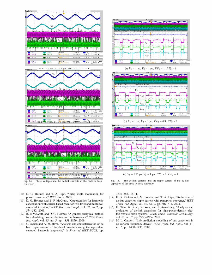
In order to verify the analysis in Section II and III, a1.5 kW back-to-back converter is built up, as shown in Fig.13. The DC capacitors contain a 900 uF electrolytic capacitorbank and a 1 uF film capacitor, where the latter one is usedto clamp the overshot of the dc bus voltage due to its muchbetter performance at high frequency. Besides, a much smallerfilm capacitor is put on the dc bus close to each phase legof both the rectifier and the inverter, in order to clamp theovershot of the dc bus voltage and protect the IGBTs. Butsince their capacitances (1 nF - 10 nF) are much smaller thanthe one with the capacitor bank, they will only draw the dclink current slightly. Thereby, the currents measured at thepoints as shown in Fig. 13 can be considered as the idealidc1, idc2, and icap. The experiment results are indicated inFig. 14 and Fig. 15, where the dc bus voltage is 250 V, thefundamental frequencies of the rectifier and the inverter are50 Hz and 40 Hz, respectively, V1 and V2 are the amplitudesof the AC voltages and indirectly represent the modulationindexes of the rectifier and the inverter, PF1 and PF2 are theirpower factors. The phase voltage, power factor, and amplitudeof the phase current of the inverter are always kept at 85 V,1, and 8 A. It can be seen that when both the amplitudes ofthe phase voltage and power factors of the rectifier and theinverter are the same, the amplitudes of the DC-link currentsidc1 and idc2 are quite close to each other (Fig. 14 (a)), wherethe small difference is due to the voltage drop on the inductorof the ac filter. The DC-link current amplitude of the rectifierwill increase when its power factor or phase voltage decreases(Fig. 14 (b) and Fig. 14 (c)). Moreover, the DC-link currentsidc1 and idc2 are always in-phase (Fig. 15 (a), (b) and (c)),because of the synchronization of the carriers. Besides, when
the amplitudes of the phase voltage and power factors are thesame, the rectifier and the inverter will have almost the samepulsed DC-link currents, in terms of the amplitude and width.Thereby, the capacitor current icap is minimized (Fig. 15 (a)).When the power factor of the converter decreases to 0.9 its DC-link current idc1 will be slightly changed on the amplitude andalso the width. At the same time, the capacitor current icap willincrease slightly (Fig. 15 (b)). A larger change can be observedon the amplitude and width of dc-link current idc1, when theAC voltage of the converter decreases to 0.75 pu, and thecapacitor current is also much larger than the other two cases(Fig. 15 (c)). The RMS values of the capacitor currents arecalculated based on the measured data, and they are 1 pu, 1.3pu and 1.8 pu (2.4 A is normalized as 1 pu) for the three casesin Fig. 15 (a), (b), and (c), respectively.
VI. CONCLUSION
New perspectives to reduce the DC-link capacitor ripplecurrent have been investigated based on a generic derivation onthe capacitor current ripple of the BTB converter. Besides thesynchronization of the pulsed dc-link currents of the rectifierstage and inverter stage of BTB converter, the theoreticalstudies reveal that the width and amplitude of the pulsed dc-link currents also have significant impact on the capacitorcurrent stresses. The factors which influence those width andamplitude are therefore identified, such as the modulationindex and the power factor. A 1.5 kW BTB converter prototypeis built and the DC-link capacitor ripple current is measuredunder different control conditions. The experimental resultsverify the theoretical expectations.
REFERENCES
[1] H. Wang, M. Liserre, and F. Blaabjerg, “Toward reliable powerelectronics: Challenges, design tools, and opportunities,” IEEEIndustrial Electronics Magazine, vol. 7, no. 2, pp. 17–26, 2013.
[2] F. Blaabjerg, K. Ma, and D. Zhou, “Power electronics andreliability in renewable energy systems,” in Proc. of ISIE, pp.19–30, 2012.
[3] C. Busca, R. Teodorescu, F. Blaabjerg, S. Munk-Nielsen,L. Helle, T. Abeyasekera, and P. Rodriguez, “An overview ofthe reliability prediction related aspects of high power igbts inwind power applications,” Microelectronics reliability, vol. 51,no. 9-11, pp. 1903–1907, 2013.
[4] H. Wang and F. Blaabjerg, “Reliability of capacitors for dc-linkapplications in power electronic converters an overview,” IEEETrans. Ind. Appl., in press.
[5] J. Dai, D. Xu, and B. Wu, “A novel control scheme for current-source-converter-based pmsg wind energy conversion systems,”IEEE Trans. Power Electron., vol. 24, no. 4, pp. 963–972, 2009.
[6] J. Yao, H. Li, Y. Liao, and Z. Chen, “An improved controlstrategy of limiting the dc-link voltage fluctuation for a doublyfed induction wind generator,” IEEE Trans. Power Electron.,vol. 23, no. 3, pp. 1205–1213, 2008.
[7] L. Gonzalez, G. Garcera, E. Figueres, and R. Gonzalez, “Effectsof the pwm carrier signals synchronization on the dc-link currentin back-to-back converters,” Applied Energy, vol. 87, no. 8, pp.2491–2499, 2010.
[8] B. G. Gu and K. Nam, “A dc-link capacitor minimizationmethod through direct capacitor current control,” IEEE Trans.Ind. Appl., vol. 42, no. 2, pp. 573–581, 2006.
[9] J. W. Kolar, T. M. Wolbank, and M. Schrodl, “Analyticalcalculation of the rms current stress on the dc link capacitorof voltage dc link pwm converter systems,” in Proc. of IEEE-EMD, pp. 81–89, 1999.
va1
va2
idc1
idc2
va1
va2
idc1
idc2
va1
va2
idc1
idc2
(a) V1 = 1 pu, V2 = 1 pu, PF1 = 1, PF2 = 1
va1
va2
idc1
idc2
va1
va2
idc1
idc2
va1
va2
idc1
idc2
(b) V1 = 1 pu, V2 = 1 pu, PF1 = 0.9, PF2 = 1
va1
va2
idc1
idc2
va1
va2
idc1
idc2
va1
va2
idc1
idc2
(c) V1 = 0.75 pu, V2 = 1 pu, PF1 = 1, PF2 = 1
Fig. 14. Phase voltages and the dc-link currents of the back to backconverter.
va1
idc1
idc2
icap
(a) V1 = 1 pu, V2 = 1 pu, PF1 = 1, PF2 = 1
va1
idc1
idc2
icap
(b) V1 = 1 pu, V2 = 1 pu, PF1 = 0.9, PF2 = 1
va1
idc1
idc2
icap
(c) V1 = 0.75 pu, V2 = 1 pu, PF1 = 1, PF2 = 1
Fig. 15. The dc-link currents and the ripple current of the dc-linkcapacitor of the back to back converter.
[10] D. G. Holmes and T. A. Lipo, “Pulse width modulation forpower converters,” IEEE Press, 2003.
[11] D. G. Holmes and B. P. McGrath, “Opportunities for harmoniccancellation with carrier-based pwm for two-level and multilevelcascaded inverters,” IEEE Trans. Ind. Appl., vol. 37, no. 2, pp.574–582, 2001.
[12] B. P. McGrath and D. G. Holmes, “A general analytical methodfor calculating inverter dc-link current harmonics,” IEEE Trans.Ind. Appl., vol. 45, no. 5, pp. 1851–1859, 2009.
[13] U. Ayhan and A. M. Hava, “Analysis and characterization of dcbus ripple current of two-level inverters using the equivalentcentered harmonic approach,” in Proc. of IEEE-ECCE, pp.
3830–3837, 2011.[14] F. D. Kieferndorf, M. Forster, and T. A. Lipo, “Reduction of
dc-bus capacitor ripple current with pam/pwm converter,” IEEETrans. Ind. Appl., vol. 40, no. 2, pp. 607–614, 2004.
[15] H. Wen, W. Xiao, X. Wen, and P. Armstrong, “Analysis andevaluation of dc-link capacitors for high-power-density elec-tric vehicle drive systems,” IEEE Trans. Vehicular Technology,vol. 61, no. 7, pp. 2950–2964, 2012.
[16] M. L. Gasperi, “Life prediction modelling of bus capacitors inac variable-frequency drives,” IEEE Trans. Ind. Appl., vol. 41,no. 6, pp. 1430–1435, 2005.