Embed Size (px)
Citation preview
Aalborg Universitet
Discrete-Time Domain Modelling of Voltage Source Inverters in StandaloneApplicationsEnhancement of Regulators Performance by Means of Smith Predictor
Federico, de Bosio; de Sousa Ribeiro, Luiz Antonio ; Freijedo Fernandez, Francisco Daniel;Pastorelli, Michele; Guerrero, Josep M.Published in:I E E E Transactions on Power Electronics
DOI (link to publication from Publisher):10.1109/TPEL.2016.2632527
Publication date:2017
Document VersionEarly version, also known as pre-print
Link to publication from Aalborg University
Citation for published version (APA):Federico, D. B., de Sousa Ribeiro, L. A., Freijedo Fernandez, F. D., Pastorelli, M., & Guerrero, J. M. (2017).Discrete-Time Domain Modelling of Voltage Source Inverters in Standalone Applications: Enhancement ofRegulators Performance by Means of Smith Predictor. I E E E Transactions on Power Electronics, 32(10), 8100- 8114 . https://doi.org/10.1109/TPEL.2016.2632527
General rightsCopyright and moral rights for the publications made accessible in the public portal are retained by the authors and/or other copyright ownersand it is a condition of accessing publications that users recognise and abide by the legal requirements associated with these rights.
- Users may download and print one copy of any publication from the public portal for the purpose of private study or research. - You may not further distribute the material or use it for any profit-making activity or commercial gain - You may freely distribute the URL identifying the publication in the public portal -
Take down policyIf you believe that this document breaches copyright please contact us at [email protected] providing details, and we will remove access tothe work immediately and investigate your claim.

www.microgrids.et.aau.dk
Abstract— The decoupling of the capacitor voltage and
inductor current has been shown to improve significantly
the dynamic performance of voltage source inverters in
standalone applications. However, the computation and
PWM delays still limit the achievable bandwidth. In this
paper a discrete-time domain modelling of the LC plant
with consideration of delay and sample-and-hold effects on
the state feedback cross-coupling decoupling is derived.
From this plant formulation, current controllers with wide
bandwidth and good relative stability properties are
developed. Two controllers based on lead compensation
and Smith predictor design, respectively, are obtained.
Subsequently, the voltage regulator is also designed for a
wide bandwidth, which permits the inclusion of resonant
filters for the steady-state mitigation of odd harmonics at
nonlinear unbalance load terminals. Discrete-time domain
implementation issues of an anti-wind up scheme are
discussed as well, highlighting the limitations of some
discretization methods. Extensive experimental results,
including a short-circuit test, verify the theoretical
analysis.
Index Terms— Current control, voltage control, power
quality
I. INTRODUCTION
HE design of voltage and current regulators for Voltage
Source Inverters (VSIs) intended for standalone
applications, i.e. islanded microgrids or Uninterruptible Power
Manuscript received March 10, 2016; revised April 24, 2016 and September 07, 2016; accepted November 14, 2016. This work was supported in part by the CNPq/Brazil and CEMAR.
Federico de Bosio and Michele Pastorelli are with the Department of Energy, Politecnico di Torino, 10124 Torino, Italy (e-mails: {federico.debosio, michele.pastorelli} @polito.it).
Luiz A. de S. Ribeiro is with the Institute of Electrical Energy, Federal University of Maranhao, Sao Luiz MA, Brazil (e-mail: [email protected]).
Francisco D. Freijedo is with the Power Electronics Laboratory, Ecole polytechnique fédérale de Lausanne, Lausanne, Switzerland (e-mail: [email protected]).
Josep M. Guerrero is with the Department of Energy Technology, Aalborg University, Aalborg, Denmark (e-mail: [email protected]).
Supply (UPS) systems, should aim to achieve good
performance during steady-state and transient conditions. This
means the system should be operated with wide stability
margins. The poor dynamics of these regulators are
responsible for degraded performance of the overall control
system. Thus effective control design and implementation of
the regulators is mandatory. In this context, four general
requirements are usually imposed on any current or voltage
regulator [1]: i) to achieve zero steady-state error; ii) to
accurately track the commanded reference and reject any
disturbance; iii) to widen the closed-loop control bandwidth as
much as possible to achieve fast transient response; iv) to
reduce the total harmonic distortion by compensating for low
order harmonics. Mandatory requirements specifically for AC
power supply/UPS systems are fault and peak current
protection [2].
A possible design of voltage or current regulators is based
on Proportional Resonant (PR) controllers in the αβ stationary
reference frame. This structure is equivalent to two
Proportional Integral (PI) controllers, one for the positive and
the other for the negative sequence in the synchronous
reference frame [3]. Independently of the PR controller
structure, the effect of delays and voltage coupling in
standalone applications should be carefully considered in the
design stage. In particular, as proved in a recent publication
[4], the coupling between the capacitor voltage and inductor
current in VSIs with LC output filter, which is usually the case
in UPS systems [5], degrades the dynamics of the inner
regulators.
A possible approach for analysis is based on s-domain
models, which are useful as they improve the general
perception of the dynamic behavior of pulse-width modulators
[6]. Subsequently, the design of the regulators in the s-domain
is followed by their discretization. However, the mapping
from the s-domain to the z-domain can introduce some
discrepancy, depending on the discretization method used [5],
[7]. On the other hand, the direct design of digital
compensators in the discrete-time domain provides more
accuracy, being able to capture the sampling effects. In fact,
the transformation of the system in the discrete-time domain
Discrete-Time Domain Modelling of Voltage
Source Inverters in Standalone Applications:
Enhancement of Regulators Performance by
Means of Smith Predictor
Federico de Bosio, Student Member, IEEE, Luiz A. de S. Ribeiro, Member, IEEE
Francisco D. Freijedo, Member, IEEE, Michele Pastorelli, Member, IEEE
and Josep M. Guerrero, Fellow Member, IEEE
T
www.microgrids.et.aau.dk
by means of z-transform or discrete-time modelling in state-
space form allows the sample-and-hold effect and time lag to
be treated accurately [8]-[11], without the need of using the
approximated rational transfer functions of the delay [12].
Moreover, the methodology presented in [13] allows the
Cross-Coupled State Equations of a system with coupled
variables and multiple feedback paths to be derived, following
a discretization approach. This is the approach to be used in
order to correctly represent the coupling between the
controlled states. In general, other advantages can be
identified for direct design in the z-domain: i) design for direct
discrete-time pole-placement [14], [15]; ii) improved dynamic
performance and robustness of the regulators [16], especially
if the ratio of the sampling frequency to the fundamental
frequency is low [14] or the current regulator is tuned for a
very wide bandwidth [17]. Accordingly, z-domain modelling
is considered convenient for an accurate design.
Usually, when voltage decoupling is performed, the
influence of compensating for computation and PWM delays
on the state feedback decoupling path is not taken into
account. In fact, in previous works, the decoupling of the
controlled states does not take into account the effect of
computation and PWM delays when performed. Specifically,
state feedback decoupling has often been used for decoupling
the cross-coupling caused by the implementation of current
controllers in the synchronous reference frame [1], for
decoupling the back-emf effect in dc [18] and ac drives [19]
(resulting in a current control strategy independent of the
speed), and for decoupling current and voltage states in dc-dc
converters [20] and UPS systems [4], [21]. Nevertheless, in
these applications the decoupling is analyzed in the continuous
time domain. Because the delays introduced by the discrete-
time modelling are not present, the resulting model used to
design and analyze the inner current loop is simply the model
of an RL load. This is equivalent to considering the
decoupling as ideal. Nevertheless, system delays significantly
degrade the performance of state feedback decoupling. As
proved in [4], the state feedback decoupling action can be
improved by leading the capacitor voltage on the state
feedback decoupling path. Moreover, the possibility to widen
the current loop bandwidth either by means of a lead
compensator on the forward path or a Smith Predictor
structure has not previously been investigated, and is the main
original proposal of this work. To the best knowledge of the
authors, no deep analyses in the discrete-time domain have
been previously provided for these kinds of techniques. As
will be shown in the paper, both structures allow good
dynamics properties to be achieved as the controller
bandwidth is widened. However, the way these techniques aim
at compensating for system delays is different. Specifically,
the lead compensator adds an additional degree of freedom to
the system in order to directly locate the poles of the closed-
loop controller transfer function. On the other hand, the Smith
predictor structure permits the design of the controller based
on the un-delayed model of the physical plant by building a
parallel model which cancels the system delay. As the current
regulator dynamics are enhanced, the voltage loop dynamics
are widened as well. In this paper it is shown how an accurate
modelling of the delay effects in decoupling leads to a better
control design and dynamics assessment.
A model in the discrete-time domain which takes into
account the coupling of the capacitor voltage with the inductor
current, even if voltage decoupling is performed, is derived
analytically. This model is shown to better represent the
physical system being addressed. It is important to note that
even without the one sample delay introduced by computation,
the sample-and-hold effect is still present and limits the
achievable bandwidth, thus reducing the benefits introduced
by the decoupling. The effect of widening the inner current
loop bandwidth by means of two techniques based on a lead
compensator structure and Smith Predictor is proposed.
Finally, the results obtained for the current loop analysis are
applied to design the voltage loop, based on the Nyquist
criterion. A straightforward mathematical formulation to select
the fundamental integral gain of the resonator by moving the
zeros of the controller to the real axis is used for practical
design.
This work is organized as follows. In Section III the model
in the discrete-time domain which takes into account the
coupling of the controlled states is derived. The devised model
is compared to the simplified formulation based on an RL load
and the main differences are discussed. In Section IV the inner
loop current control with state feedback voltage decoupling is
analyzed. Two techniques aimed to widen the bandwidth of
the current regulator, based on a lead compensator structure
and Smith Predictor, are proposed and compared.
Subsequently, in Section V, a PR voltage controller design is
proposed based on the design of the current regulator with
wide bandwidth. Detailed design and tuning is provided
according to the Nyquist criterion. Moreover, discretization
issues of an anti-wind up scheme for the voltage regulator are
analyzed. In Section VI the theoretical solution is supported
by experimental results, verifying their compliance with the
IEC 62040 normative for UPS systems.
II. SYSTEM DESCRIPTION
In standalone applications, the VSI is implemented with an
LC filter at its output. In general, it operates in voltage control
mode with the capacitor voltage and inductor currents being
the controlled states. Fig. 1 shows the block diagram
representation including a three-phase power converter with
its inner loops. The inner current loop has to track the
commands provided by the outer voltage loop and to ensure
disturbance rejection within its bandwidth [17], [22].
The simplified block diagram representation of the closed-
loop system is shown in Fig. 2, where 𝑽𝐶𝛼𝛽∗ = 𝑉𝐶𝛼
∗ + 𝑗𝑉𝐶𝛽∗
and 𝑰𝐿𝛼𝛽∗ = 𝐼𝐿𝛼
∗ + 𝑗𝐼𝐿𝛽∗
are the voltage and current reference
vectors and 𝑰𝑜𝛼𝛽 = 𝐼𝑜𝛼 + 𝑗𝐼𝑜𝛽 is the output current vector,
which acts as a disturbance to the system. 𝐺𝑖(𝑧) and 𝐺𝑣(𝑧)represent the current and voltage regulators transfer functions
(TF) in the discrete-time domain. There is one sample
computational delay associated to the implemented regular
sampled symmetrical PWM strategy, i.e. the time required to

www.microgrids.et.aau.dk
compute the duty-cycle control signal [9], [23]. 𝐺𝑑𝑒𝑐(𝑧) is the
TF related to the decoupling of the cross-coupling controlled
states. The capacitor 𝐶𝑓 = 3𝐶 is the equivalent capacitance of
a Y connection configuration.
abcab
abcab
vdc
+
-
Lf
Lf
Lf
iLa
iLb
iLc
iLab
Load
vCab
+-
+- *
abcab
PWM
iLab vCab*
ioa
iob
ioc
Reference
generator
Cf
Cf
Cf
Gi(z) Gv(z)
Fig. 1. Block diagram of a three phase VSI with voltage and current loops.
- z
-1
Rf
1
s
1
Lf
+ iab
ioab
+- 1
s
1
Cf
vab-
Iab +
-
*Vab
*+
-
Gdec(z)
+
+
Regulators Physical Plant
decoupling Ts
L
A
T
C
H
delay
Gi(z)Gv(z)
Fig. 2. Simplified block diagram of the closed-loop system.
III. DISCRETE-TIME DOMAIN PLANT MODELLING
As voltage decoupling is performed, higher damping is
achieved with less overshoot for a given bandwidth [4]. If it
was possible to exactly decouple (cancel) the capacitor
coupling, the system would become not dependent on the load
impedance and the physical plant could be represented by an
RL load. In this case, the modelling in the discrete-time
domain is based on the Z-transform of the part of the plant
related to the inductor current 𝐺𝑝(𝑠) along with the sample-
and-hold effect [10], leading to
𝐺𝑝(𝑧) =𝑰𝐿𝛼𝛽
𝑽𝑖𝛼𝛽= 𝒁{𝑳{𝐿𝑎𝑡𝑐ℎ}𝐺𝑝(𝑧)} =
= (1 − 𝑧−1)𝒁 {𝐺𝑝(𝑠)
𝑠} =
1
𝑅𝑓
(1 − 𝑒−𝑇𝑠/𝜏𝑝)𝑧−1
1 − 𝑒−𝑇𝑠/𝜏𝑝𝑧−1. (1)
Where 𝑰𝐿𝛼𝛽(𝑧) and 𝑽𝑖𝛼𝛽(𝑧) are the inductor current and
input voltage in the z-domain, respectively; 𝜏𝑝 = 𝐿𝑓/𝑅𝑓 is the
plant time-constant. However, the coupling effect introduced
by the second-order LC filter cannot be neglected, because of
computation and PWM delays which are not fully
compensated for on the state feedback decoupling path. Even
without the one sample delay introduced by computation, the
latch interface is still present, not allowing the complete
decoupling of the controlled states. The effect of capacitor
voltage in the dynamics should be considered in the design
stage [24]. For this reason, a model which reflects this effect
has been developed. The general methodology, here reported,
is similarly applied in [13].
Step 1: Model and derive the Ordinary Differential
Equations (ODEs) of the system;
Step 2: Form the Laplace transform of the ODEs including
the effects of initial conditions;
Step 3: Form a step input for the latched manipulated input;
Step 4: Find the continuous time step response solution;
Step 5: Find the response at the next sampling instant;
Step 6: Generalize the solution for arbitrary sampling
instants (𝑘𝑇);
Step 7: Form eventually the correspondent transfer function
in the discrete-time domain.
With reference to Fig. 3 and neglecting the disturbance
𝑖𝑜(𝑡), the ODEs of the system are
{
𝑑
𝑑𝑡𝑣𝑐(𝑡) =
1
𝐶𝑓𝑖𝐿(𝑡)
𝑑
𝑑𝑡𝑖𝐿(𝑡) =
1
𝐿𝑓[𝑣𝑖(𝑡) − 𝑅𝑖𝐿(𝑡) − 𝑣𝑐(𝑡)].
(2)
The equivalent series resistance (ESR) of the filter capacitor
𝐶𝑓 is not considered in the model, since its effect appears far
above the frequency range of concern [25], it is usually small
and has little effect in dynamics. The system in (2) is
transformed in the Laplace domain including the effects of
initial conditions, fundamental to derive the Cross-Coupled
State Equations. The sample-and-hold effect is modelled as
𝑉𝑖(𝑠) = 𝑣𝑖(𝑡 = 0)/𝑠 (input modelled as steps). In particular
the relationships between the states are
𝑉𝑐(𝑠) =𝜔𝑛2
𝑠2 + 2𝜉𝜔𝑛𝑠 + 𝜔𝑛2{𝑣𝑖(𝑡 = 0)
1
𝑠
+1
𝜔𝑛2[𝑠𝑣𝑐(𝑡 = 0) + �̇�𝑐(𝑡 = 0)]
+2𝜉
𝜔𝑛𝑣𝑐(𝑡 = 0)}.
(3)
𝐼𝐿(𝑠) =𝜔𝑛2
𝑠2 + 2𝜉𝜔𝑛𝑠 + 𝜔𝑛2[𝐶𝑓𝑣𝑖(𝑡 = 0)
+ 𝐿𝑓𝐶𝑓𝑠𝑖𝐿(𝑡 = 0) − 𝐶𝑓𝑣𝑐(𝑡 = 0)].
(4)
Where
𝜔𝑛2 =
1
𝐿𝑓𝐶𝑓; 𝜉 =
1
2𝜔𝑛
𝑅𝑓
𝐿𝑓=𝑅𝑓
2√𝐶𝑓
𝐿𝑓. (5)
Being 𝜔𝑛 the natural frequency of the plant and 𝜉 the
damping factor. Then the inverse Laplace transform is applied
to (3) and (4). The continuous time step response is
generalized for arbitrary sampling instants, followed by the
transformations to the z-domain and αβ stationary reference
frame. More details are provided in Appendix. The Cross-
Coupled State Equations are thus obtained
𝑽𝑐𝛼𝛽(𝑧) [1 +𝜔𝑛𝜔𝑑
𝑒−𝜉𝜔𝑛𝑇 sin(𝜔𝑑𝑇 − 𝜙)𝑧−1
−2𝜉𝜔𝑛𝜔𝑑
𝑒−𝜉𝜔𝑛𝑇sin(𝜔𝑑𝑇)𝑧−1]
= [1 −𝜔𝑛𝜔𝑑
𝑒−𝜉𝜔𝑛𝑇 𝑠𝑖𝑛(𝜔𝑑𝑇 + 𝜙)]𝑽𝑖𝛼𝛽(𝑧)𝑧−1
+1
𝐶𝑓𝜔𝑑𝑒−𝜉𝜔𝑛𝑇 𝑠𝑖𝑛(𝜔𝑑𝑇) 𝑰𝐿𝛼𝛽(𝑧)𝑧
−1.
(6)
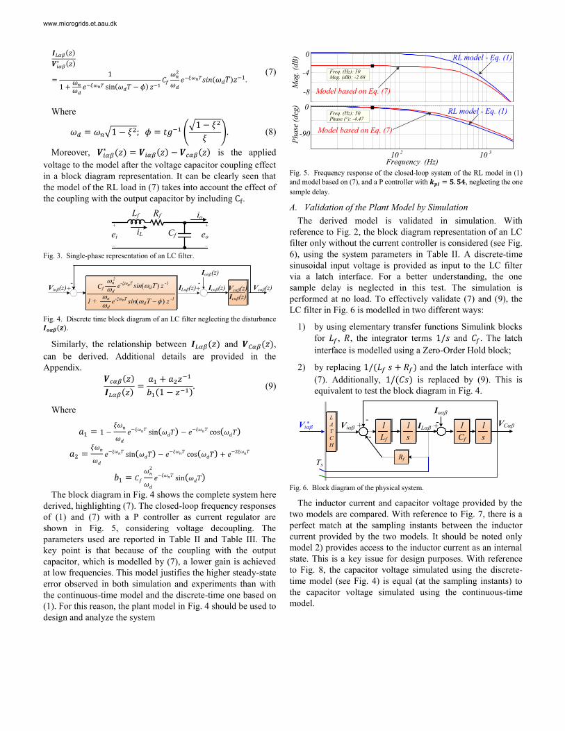
www.microgrids.et.aau.dk
𝑰𝐿𝛼𝛽(𝑧)
𝑽𝑖𝛼𝛽∗ (𝑧)
=1
1 +𝜔𝑛𝜔𝑑
𝑒−𝜉𝜔𝑛𝑇 sin(𝜔𝑑𝑇 − 𝜙) 𝑧−1𝐶𝑓𝜔𝑛2
𝜔𝑑𝑒−𝜉𝜔𝑛𝑇𝑠𝑖𝑛(𝜔𝑑𝑇)𝑧
−1. (7)
Where
𝜔𝑑 = 𝜔𝑛√1 − 𝜉2; 𝜙 = 𝑡𝑔−1 (
√1 − 𝜉2
𝜉). (8)
Moreover, 𝑽𝑖𝛼𝛽∗ (𝑧) = 𝑽𝑖𝛼𝛽(𝑧) − 𝑽𝑐𝛼𝛽(𝑧) is the applied
voltage to the model after the voltage capacitor coupling effect
in a block diagram representation. It can be clearly seen that
the model of the RL load in (7) takes into account the effect of
the coupling with the output capacitor by including Cf.
Lf
iL Cf
Rf io
ei eo
Fig. 3. Single-phase representation of an LC filter.
+ ILαβ(z)
Ioαβ(z)
+-
Icαβ(z) Vcαβ(z)
Icαβ(z)
Vcαβ(z)-
Viαβ(z)
n1 + e-xwT
sin(wdT-f)z -1wn
wd
nCf
wn
wd
2
e-xwT
sin(wdT)z -1
Fig. 4. Discrete time block diagram of an LC filter neglecting the disturbance
𝑰𝒐𝜶𝜷(𝒛).
Similarly, the relationship between 𝑰𝐿𝛼𝛽(𝑧) and 𝑽𝐶𝛼𝛽(𝑧),
can be derived. Additional details are provided in the
Appendix.
𝑽𝑐𝛼𝛽(𝑧)
𝑰𝐿𝛼𝛽(𝑧)=𝑎1 + 𝑎2𝑧
−1
𝑏1(1 − 𝑧−1)
. (9)
Where
𝑎1 = 1 −𝜉𝜔𝑛
𝜔𝑑𝑒−𝜉𝜔𝑛𝑇 sin(𝜔𝑑𝑇) − 𝑒
−𝜉𝜔𝑛𝑇 cos(𝜔𝑑𝑇)
𝑎2 =𝜉𝜔𝑛
𝜔𝑑𝑒−𝜉𝜔𝑛𝑇 sin(𝜔𝑑𝑇) − 𝑒
−𝜉𝜔𝑛𝑇 cos(𝜔𝑑𝑇) + 𝑒−2𝜉𝜔𝑛𝑇
𝑏1 = 𝐶𝑓𝜔𝑛2
𝜔𝑑𝑒−𝜉𝜔𝑛𝑇 sin(𝜔𝑑𝑇)
The block diagram in Fig. 4 shows the complete system here
derived, highlighting (7). The closed-loop frequency responses
of (1) and (7) with a P controller as current regulator are
shown in Fig. 5, considering voltage decoupling. The
parameters used are reported in Table II and Table III. The
key point is that because of the coupling with the output
capacitor, which is modelled by (7), a lower gain is achieved
at low frequencies. This model justifies the higher steady-state
error observed in both simulation and experiments than with
the continuous-time model and the discrete-time one based on
(1). For this reason, the plant model in Fig. 4 should be used to
design and analyze the system
Ph
ase
(d
eg)
-90
0
0
-4
-8
Ma
g. (d
B)
102
103
Frequency (Hz)
Model based on Eq. (7)
Model based on Eq. (7)
RL model - Eq. (1)
RL model - Eq. (1)
Freq. (Hz): 50Mag. (dB): -2.68
Freq. (Hz): 50Phase (°): -4.47
Fig. 5. Frequency response of the closed-loop system of the RL model in (1)
and model based on (7), and a P controller with 𝒌𝒑𝑰 = 𝟓.𝟓𝟒, neglecting the one
sample delay.
A. Validation of the Plant Model by Simulation
The derived model is validated in simulation. With
reference to Fig. 2, the block diagram representation of an LC
filter only without the current controller is considered (see Fig.
6), using the system parameters in Table II. A discrete-time
sinusoidal input voltage is provided as input to the LC filter
via a latch interface. For a better understanding, the one
sample delay is neglected in this test. The simulation is
performed at no load. To effectively validate (7) and (9), the
LC filter in Fig. 6 is modelled in two different ways:
1) by using elementary transfer functions Simulink blocks
for 𝐿𝑓, 𝑅, the integrator terms 1/𝑠 and 𝐶𝑓. The latch
interface is modelled using a Zero-Order Hold block;
2) by replacing 1/(𝐿𝑓 𝑠 + 𝑅𝑓) and the latch interface with
(7). Additionally, 1/(𝐶𝑠) is replaced by (9). This is
equivalent to test the block diagram in Fig. 4.
-
Rf
1
s
1
Lf
+ ILab
Ioab
+- 1
s
1
Cf
VCab-
Viab*
Ts
L
A
T
C
H
Viab
Fig. 6. Block diagram of the physical system.
The inductor current and capacitor voltage provided by the
two models are compared. With reference to Fig. 7, there is a
perfect match at the sampling instants between the inductor
current provided by the two models. It should be noted only
model 2) provides access to the inductor current as an internal
state. This is a key issue for design purposes. With reference
to Fig. 8, the capacitor voltage simulated using the discrete-
time model (see Fig. 4) is equal (at the sampling instants) to
the capacitor voltage simulated using the continuous-time
model.

www.microgrids.et.aau.dk
Time (s)0.04 0.08 0.120
Curr
ent
(A)
0
-0.2
0.2
0.12
0.02
0.02 0.024
Discretetime-domain
Continuoustime-domain
Fig. 7. Inductor current (α-axis) - Comparison of modelling: TF Simulink
blocks (plant modelling in the continuous time-domain); current simulated by using the derived model (block diagram showed in Fig. 4).
0
-10
10
Time (s)0.04 0.08 0.120
0.06 0.061
3
0
Vo
lta
ge
(V)
Continuoustime-domain
Discretetime-domain
Fig. 8. Capacitor voltage (α-axis) - Comparison of modelling: TF Simulink
blocks (plant modelling in the continuous time-domain); voltage simulated by using the derived model (block diagram showed in Fig. 4).
A more rigorous validation is based on applying, in open
loop, the actual pulse-width modulated voltage provided by a
three-phase power converter to an LC filter at no load
conditions. Again, the one sample delay is not included in the
analysis. In order to mitigate non-linearity effects introduced
by PWM, the physical parameters in Table I are used to
perform the simulation. The results are compared with those
provided by the model based on (7) and (9).
2
0
-40.06 0.061
60
20
0
-20
Time (s)0.04 0.080
Cu
rren
t (A
)
Fig. 9. Inductor current - Comparison of modelling: pulse-width modulated
simulation; current simulated by using the derived model in the natural
reference frame (block diagram showed in Fig. 4).
Vo
lta
ge
(V)
600
200
-200
-600
0
-100
-2600.06 0.061
Time (s)0.04 0.080
Fig. 10. Capacitor voltage - Comparison of modelling: pulse-width modulated
simulation; current simulated by using the derived model in the natural reference frame (block diagram showed in Fig. 4).
With reference to Fig. 9 and Fig. 10, it can be seen the
average value of the controlled states provided by the two
models are equivalent. In fact, by using synchronous
sampling, the average value, mainly of the inductor current, is
used for control purposes. All these results demonstrate the
correctness of the devised model, which can be used for
design purposes. TABLE I
SYSTEM PARAMETERS FOR SIMULATION PURPOSES
Parameter Value
Switching frequency 𝑓𝑠 = 10 𝑘𝐻𝑧Filter inductance 𝐿𝑓 = 1.8 𝑚𝐻
Filter capacitor 𝐶𝑓 = 108 µ𝐹
Inductor ESR 𝑅 = 10 𝛺
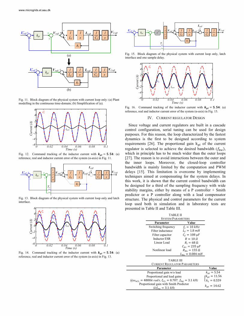
To investigate the effect of the latch interface and one
sample delay on the closed-loop TF, three different models
with the inner current loop only and a P controller as regulator
are considered (see Fig. 11, Fig. 13 and Fig. 15). The
parameters in Table II and Table III are used for analysis. As
the latch interface and one sample delay are neglected [see
Fig. 11(a)], the physical system as seen from the controller
simplifies to an RL load [see Fig. 11(b)]. This means the state
feedback decoupling path perfectly cancels out the physical
coupling of the capacitor voltage. As a consequence, the
reference current is properly tracked with almost zero steady-
state error (see Fig. 12). On the other hand, as the latch
interface is included (see Fig. 13) the steady-state error
between the reference and real inductor current increases (see
Fig. 14). Given the reference current at f = 50 Hz in α-axis
iα∗ = 5 A, the real inductor current is iα = 3.68 A. This means
iα = 0.736 iα∗ , which corresponds to -2.68 dB, in accordance
with the frequency response analysis at 50 Hz of Fig. 5.
Additionally, with reference to Fig. 15, it can be seen the
combined effect of the one sample delay and latch interface.
An even higher steady-state error is observed (see Fig. 16),
limiting the current loop control bandwidth. As Fig. 13 and
Fig. 15 implement the plant modelling previously verified in
Fig. 7 and Fig. 8, it can be concluded that state feedback
decoupling is far from being ideal. Thus, a design procedure
based on (7) and (9) provides a more accurate pole placement.
www.microgrids.et.aau.dk
-
Rf
1
s
1
Lf
+ ILab 1
s
1
Cf
VCab-
ILab+
-
* +
+
Viab
-
Rf
1
s
1
Lf
+ ILabILab+
-
* Viab
(a)
(b)
kpi
kpi
1
s
1
Cf
VCab
Fig. 11. Block diagram of the physical system with current loop only: (a) Plant modelling in the continuous time-domain; (b) Simplification of (a).
6
4
2
0
-2
-4
-60 0.02 0.04 0.06 0.08 0.1
Cur
rent
(A
)
Time (s)
iα*
iα
ierr
Fig. 12. Command tracking of the inductor current with 𝒌𝒑𝑰 = 𝟓.𝟓𝟒: (a)
reference, real and inductor current error of the system (α-axis) in Fig. 11.
-kpi
Rf
1
s
1
Lf
+ ILab
Ioab
+- 1
s
1
Cf
VCab-
ILab +
-
* +
+
Ts
L
A
T
C
H
Viab
Fig. 13. Block diagram of the physical system with current loop only and latch
interface.
6
4
2
0
-2
-4
-60 0.02 0.04 0.06 0.08 0.1
Cu
rren
t (A
)
Time (s)
iα*
iα
ierr
Fig. 14. Command tracking of the inductor current with 𝒌𝒑𝑰 = 𝟓.𝟓𝟒: (a)
reference, real and inductor current error of the system (α-axis) in Fig. 13.
z-1
-kpi
Rf
1
s
1
Lf
+ ILab
Ioab
+- 1
s
1
Cf
VCab-
ILab +
-
* +
+
Ts
L
A
T
C
H
Viab
Fig. 15. Block diagram of the physical system with current loop only, latch
interface and one sample delay.
6
4
2
0
-2
-4
-60 0.02 0.04 0.06 0.08 0.1
Cur
rent
(A
)
Time (s)
iα*
iα
ierr
Fig. 16. Command tracking of the inductor current with 𝒌𝒑𝑰 = 𝟓.𝟓𝟒: (a)
reference, real and inductor current error of the system (α-axis) in Fig. 15.
IV. CURRENT REGULATOR DESIGN
Since voltage and current regulators are built in a cascade
control configuration, serial tuning can be used for design
purposes. For this reason, the loop characterized by the fastest
dynamics is the first to be designed according to system
requirements [26]. The proportional gain kpI of the current
regulator is selected to achieve the desired bandwidth (𝑓𝑏𝑤),which in principle has to be much wider than the outer loops
[27]. The reason is to avoid interactions between the outer and
the inner loops. Moreover, the closed-loop controller
bandwidth is mainly limited by the computation and PWM
delays [15]. This limitation is overcome by implementing
techniques aimed at compensating for the system delays. In
this work, it is shown that the current control bandwidth can
be designed for a third of the sampling frequency with wide
stability margins, either by means of a P controller + Smith
predictor or a P controller along with a lead compensator
structure. The physical and control parameters for the current
loop used both in simulation and in laboratory tests are
presented in Table II and Table III.
TABLE II
SYSTEM PARAMETERS
Parameter Value
Switching frequency 𝑓𝑠 = 10 𝑘𝐻𝑧Filter inductance 𝐿𝑓 = 1.8 𝑚𝐻
Filter capacitor 𝐶𝑓 = 108 µ𝐹
Inductor ESR 𝑅 = 10 𝛺 Linear Load 𝑅𝑙 = 68 Ω
𝐶𝑁𝐿 = 235 µ𝐹 Nonlinear load 𝑅𝑁𝐿 = 155 Ω
𝐿𝑁𝐿 = 0.084 𝑚𝐻
TABLE III
CURRENT REGULATOR PARAMETERS
Parameter Value
Proportional gain w/o lead 𝑘𝑝𝐼 = 5.54
Proportional and lead gains
@𝜔𝑛𝐶𝐿 = 4800𝜋 rad/s, 𝜉𝐶𝐿 = 0.707, 𝑓𝑏𝑤 = 3.1 kHz {𝑘𝑝𝐼 = 11.56
𝑘𝐿 = 0.559Proportional gain with Smith Predictor
@𝑓𝑏𝑤 = 3.1 kHz𝑘𝑝𝐼 = 14.62
www.microgrids.et.aau.dk
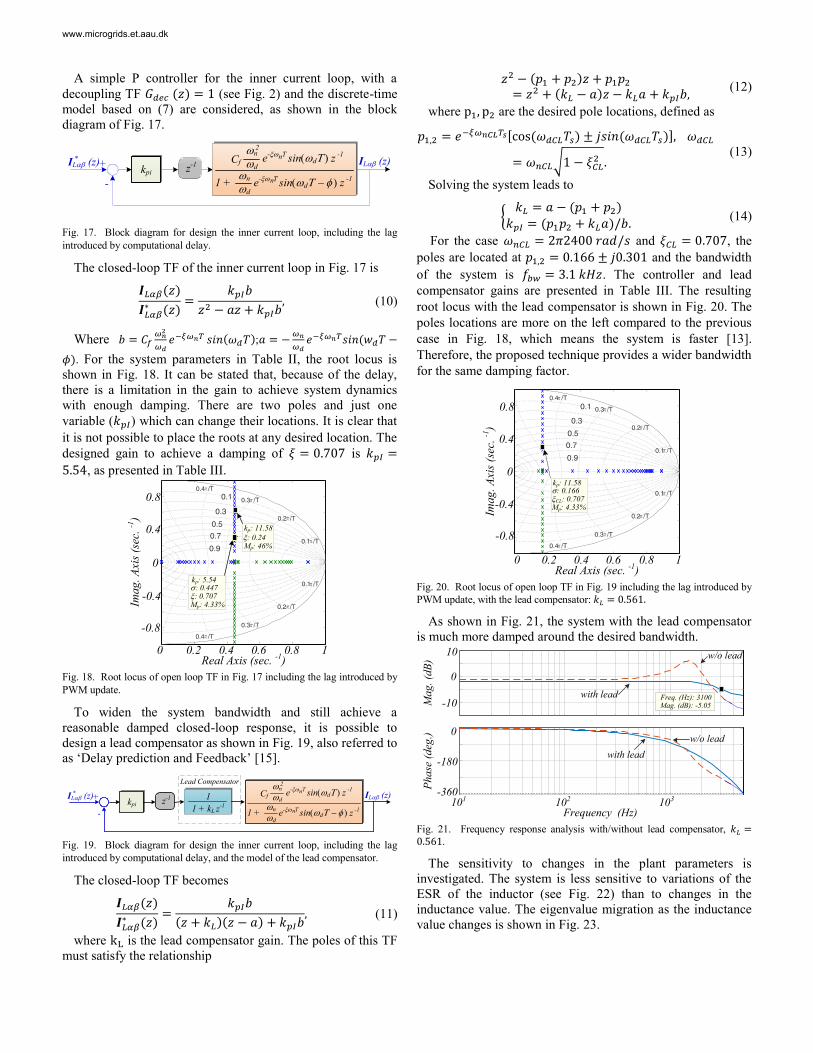
A simple P controller for the inner current loop, with a
decoupling TF 𝐺𝑑𝑒𝑐 (𝑧) = 1 (see Fig. 2) and the discrete-time
model based on (7) are considered, as shown in the block
diagram of Fig. 17.
ILab (z)ILab (z)+
-
*
z-1
n1 + e-xwT
sin(wdT-f)z -1wn
wd
nCf
wn
wd
2
e-xwT
sin(wdT)z -1
kpi
Fig. 17. Block diagram for design the inner current loop, including the lag
introduced by computational delay.
The closed-loop TF of the inner current loop in Fig. 17 is
𝑰𝐿𝛼𝛽(𝑧)
𝑰𝐿𝛼𝛽∗ (𝑧)
=𝑘𝑝𝐼𝑏
𝑧2 − 𝑎𝑧 + 𝑘𝑝𝐼𝑏, (10)
Where 𝑏 = 𝐶𝑓𝜔𝑛2
𝜔𝑑𝑒−𝜉𝜔𝑛𝑇 𝑠𝑖𝑛(𝜔𝑑𝑇);𝑎 = −
𝜔𝑛
𝜔𝑑𝑒−𝜉𝜔𝑛𝑇𝑠𝑖𝑛(𝑤𝑑𝑇 −
𝜙). For the system parameters in Table II, the root locus is
shown in Fig. 18. It can be stated that, because of the delay,
there is a limitation in the gain to achieve system dynamics
with enough damping. There are two poles and just one
variable (𝑘𝑝𝐼) which can change their locations. It is clear that
it is not possible to place the roots at any desired location. The
designed gain to achieve a damping of 𝜉 = 0.707 is 𝑘𝑝𝐼 =
5.54, as presented in Table III.
0 0.2 0.4 0.6 0.8 1Real Axis (sec.
-1)
0
0.8
0.4
-0.4
-0.8
Ima
g.
Axi
s (s
ec.
-1)
0.1 /T
0.2 /T
0.3 /T
0.4 /T
0.1 /T
0.2 /T
0.3 /T
0.4 /T
0.7
0.5
0.3
0.1
0.9
s: 0.447
Mp: 4.33%x: 0.707
kp: 5.54
Mp: 46%x: 0.24
kp: 11.58
Fig. 18. Root locus of open loop TF in Fig. 17 including the lag introduced by
PWM update.
To widen the system bandwidth and still achieve a
reasonable damped closed-loop response, it is possible to
design a lead compensator as shown in Fig. 19, also referred to
as ‘Delay prediction and Feedback’ [15].
Lead Compensator
1
1 + kL z-1
ILab (z)ILab (z)+
-
*
z-1
n1 + e-xwT
sin(wdT-f)z -1wn
wd
nCf
wn
wd
2
e-xwT
sin(wdT)z -1
kpi
Fig. 19. Block diagram for design the inner current loop, including the lag
introduced by computational delay, and the model of the lead compensator.
The closed-loop TF becomes
𝑰𝐿𝛼𝛽(𝑧)
𝑰𝐿𝛼𝛽∗ (𝑧)
=𝑘𝑝𝐼𝑏
(𝑧 + 𝑘𝐿)(𝑧 − 𝑎) + 𝑘𝑝𝐼𝑏, (11)
where kL is the lead compensator gain. The poles of this TF
must satisfy the relationship
𝑧2 − (𝑝1 + 𝑝2)𝑧 + 𝑝1𝑝2= 𝑧2 + (𝑘𝐿 − 𝑎)𝑧 − 𝑘𝐿𝑎 + 𝑘𝑝𝐼𝑏,
(12)
where p1, p2 are the desired pole locations, defined as
𝑝1,2 = 𝑒−𝜉𝜔𝑛𝐶𝐿𝑇𝑠[cos (𝜔𝑑𝐶𝐿𝑇𝑠) ± 𝑗𝑠𝑖𝑛(𝜔𝑑𝐶𝐿𝑇𝑠)], 𝜔𝑑𝐶𝐿
= 𝜔𝑛𝐶𝐿√1 − 𝜉𝐶𝐿2 .
(13)
Solving the system leads to
{𝑘𝐿 = 𝑎 − (𝑝1 + 𝑝2)
𝑘𝑝𝐼 = (𝑝1𝑝2 + 𝑘𝐿𝑎)/𝑏. (14)
For the case 𝜔𝑛𝐶𝐿 = 2𝜋2400 𝑟𝑎𝑑/𝑠 and 𝜉𝐶𝐿 = 0.707, the
poles are located at 𝑝1,2 = 0.166 ± 𝑗0.301 and the bandwidth
of the system is 𝑓𝑏𝑤 = 3.1 𝑘𝐻𝑧. The controller and lead
compensator gains are presented in Table III. The resulting
root locus with the lead compensator is shown in Fig. 20. The
poles locations are more on the left compared to the previous
case in Fig. 18, which means the system is faster [13].
Therefore, the proposed technique provides a wider bandwidth
for the same damping factor.
1
0.1 /T
0.2 /T
0.3 /T
0.4 /T
0.1 /T
0.2 /T
0.3 /T
0.4 /T
0.7
0.5
0.3
0.1
0.9
s: 0.166
Mp: 4.33%xCL: 0.707
kp: 11.58
0
0.8
0.4
-0.4
-0.8
Imag. A
xis
(sec
. -1
)
0 0.2 0.4 0.6 0.8Real Axis (sec.
-1)
Fig. 20. Root locus of open loop TF in Fig. 19 including the lag introduced by
PWM update, with the lead compensator: 𝑘𝐿 = 0.561.
As shown in Fig. 21, the system with the lead compensator
is much more damped around the desired bandwidth.
1031 102
Frequency (Hz)10
Ph
ase
(d
eg.)
-180
0
-360
Ma
g.
(dB
)
10
0
-10Freq. (Hz): 3100Mag. (dB): -5.05
with lead
w/o lead
w/o lead
with lead
Fig. 21. Frequency response analysis with/without lead compensator, 𝑘𝐿 =0.561.
The sensitivity to changes in the plant parameters is
investigated. The system is less sensitive to variations of the
ESR of the inductor (see Fig. 22) than to changes in the
inductance value. The eigenvalue migration as the inductance
value changes is shown in Fig. 23.

IEEE TRANSACTIONS ON POWER ELECTRONICS
0.9
0.7
0.5
0.3
0.1
0.4 /T
0.3 /T
0.2 /T
0.1 /T
0.4 /T
0.3 /T
0.2 /T
0.1 /T
0 0.2 0.4 0.6 0.8 1Real Axis (sec.
-1)
0
0.8
0.4
-0.4
-0.8
Ima
g.
Axi
s (s
ec.
-1)
Rrated
R
R
Fig. 22. Eigenvalue migration as a function of variation in 𝑅𝑟𝑎𝑡𝑒𝑑 = 0.1 𝛺 →𝑅 = 2 𝛺.
0.9
0.7
0.5
0.3
0.1
0.4 /T
0.3 /T
0.2 /T
0.1 /T
0.4 /T
0.3 /T
0.2 /T
0.1 /T
L
L
Lrated
0 0.2 0.4 0.6 0.8 1Real Axis (sec.
-1)
0
0.8
0.4
-0.4
-0.8
Imag. A
xis
(sec
. -1
)
Fig. 23. Eigenvalue migration as a function of variation in 𝐿 = 0.9 𝑚𝐻 →2𝐿𝑟𝑎𝑡𝑒𝑑 = 3.6 𝑚𝐻.
Another technique aimed at widening the bandwidth of the
current regulator while still achieving good dynamic
properties is based on the Smith Predictor structure [28]. The
basic idea is to build a parallel model which cancels the
system delay (see Fig. 24). In this way, the design of the
controller can be performed using the un-delayed model of the
plant. Robustness issues must be considered with this method.
If there is any model error, especially in the delay itself, the
Smith predictor can degrade the system performance. These
aspects are verified in the experiments by changing the
predicted values of the plant and computation delay.
ILab (z)ILab (z)+
-
*
z-1
n1 + e-xwT
sin(wdT-f)z -1wn
wd
nCf
wn
wd
2
e-xwT
sin(wdT)z -1
+
+
+-
Smith Predictor
kpi
z-1
GP(z)
GP(z)
Fig. 24. Block diagram for design the inner current loop, including the lag
introduced by computational delay, and the model of the Smith Predictor.
The root locus of the system is shown in Fig. 25. In detail,
the closed-loop pole corresponding to 𝑓𝑏𝑤 = 3.1 𝑘𝐻𝑧 is
highlighted and the correspondent gain is reported also in
Table II. Since the un-delayed model of the plant is
considered, the design is made for a first-order system.
1
0.1 /T
0.2 /T
0.3 /T
0.4 /T
0.1 /T
0.2 /T
0.3 /T
0.4 /T
0.7
0.5
0.3
0.1
0.9
s: 0.22kp: 12.6
0 0.2 0.4 0.6 0.8Real Axis (sec.
-1)
0
0.8
0.4
-0.4
-0.8
Ima
g.
Axi
s (s
ec.
-1)
Fig. 25. Root locus of open loop TF in Fig. 24 including the lag introduced by PWM update, with the Smith Predictor.
For the same damping the system response can be made
faster than the model with the lead compensator, as can be
seen by the step response in Fig. 26.
P controller with lead compensatorP controller with Smith Predictor
0.8
0.6
0.4
0.2A
mp
litu
de
(p.u
.)
200 400 600 800 10000Time (µs)
1
Fig. 26. Step response with the lead compensator (𝑘𝐿 = 0.561) and the Smith
predictor for 𝑓𝑏𝑤 = 3.1 𝑘𝐻𝑧.
V. VOLTAGE REGULATOR DESIGN
The voltage regulator is based on PR controllers with a lead
compensator structure. The inner current loop is based on a P
controller, e.g. employed in [29], [25], along with Smith
Predictor. The addition of resonant filters provides a good
steady-state tracking of the fundamental component and
mitigates the main harmonics associated to nonlinear loads.
The gains of the system are selected to provide also a good
dynamic response when the system is tested according to the
requirements imposed by the normative for islanded systems.
The voltage regulator TF is
𝐺𝑣(𝑠) = 𝑘𝑝𝑉 + ∑ 𝑘𝑖𝑉,ℎℎ=1,5,7
𝑠 cos(𝜑ℎ) − ℎ𝜔1sin (𝜑ℎ)
𝑠2 + (ℎ𝜔1)2
. (15)
The proportional gain 𝑘𝑝𝑉 determines the bandwidth of the
voltage regulator. In order for the cascaded loops to be
effective, the inner current loop time constant should be lower
than that of the voltage loop by one fourth up to one tenth
[30]. As the effects of the delays are well compensated with
the proposed P + Smith predictor for the inner controller, high
bandwidth with wide stability margins is achieved. This
allows the selection of a low outer over inner bandwidth ratio.
According to [30] the minimum ratio is chosen and thus the
voltage regulator is designed for around 700 Hz of bandwidth.
The phase-leading angles at each harmonic frequency are set
such that the trajectories of the open loop system on the
IEEE TRANSACTIONS ON POWER ELECTRONICS
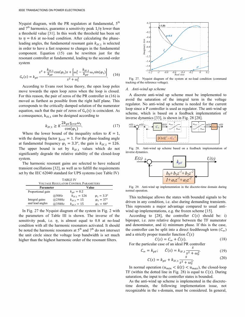
Nyquist diagram, with the PR regulators at fundamental, 5th
and 7th
harmonics, guarantee a sensitivity peak 1/𝜂 lower than
a threshold value [31]. In this work the threshold has been set
to 𝜂 = 0.6 at no-load condition. After calculating the phase-
leading angles, the fundamental resonant gain 𝑘𝑖𝑉,1 is selected
in order to have a fast response to changes in the fundamental
component. Equation (15) can be rewritten just for the
resonant controller at fundamental, leading to the second-order
system
𝐺𝑣(𝑠) = 𝑘𝑝𝑉
𝑠2 +𝑘𝑖𝑉,1𝑘𝑝𝑉
cos(𝜑1)𝑠 + [𝜔12 −
𝑘𝑖𝑉,1𝑘𝑝𝑉
ω1sin (𝜑1)]
𝑠2 + 𝜔12 .
(16)
According to Evans root locus theory, the open loop poles
move towards the open loop zeros when the loop is closed.
For this reason, the pair of zeros of the PR controller in (16) is
moved as furthest as possible from the right half plane. This
corresponds to the critically damped solution of the numerator
equation, such that the pair of zeros of Gv(s) is coincident. As
a consequence, kiV,1 can be designed according to
𝑘𝑖𝑉,1 ≥ 𝐾2𝑘𝑝𝑉ƺ𝑐𝑟𝑖𝑡𝜔1
cos(𝜑1). (17)
Where the lower bound of the inequality refers to 𝐾 = 1,
with the damping factor ƺ𝑐𝑟𝑖𝑡 = 1. For the phase-leading angle
at fundamental frequency 𝜑1 = 3.3°, the gain is 𝑘𝑖𝑉,1 = 126.
The upper bound is set by 𝑘𝑖𝑉,1 values which do not
significantly degrade the relative stability of the closed-loop
system.
The harmonic resonant gains are selected to have reduced
transient oscillations [32], as well as to fulfill the requirements
set by the IEC 62040 standard for UPS systems (see Table IV)
TABLE IV VOLTAGE REGULATOR CONTROL PARAMETERS
Parameter Value
Proportional gain 𝑘𝑝𝑉 = 0.2
@50Hz 𝑘𝑖𝑉,1 = 126 𝜑1 = 3.3° Integral gains and lead angles
@250Hz 𝑘𝑖𝑉,5 = 15 𝜑5 = 37°
@350Hz 𝑘𝑖𝑉,7 = 15 𝜑7 = 44°
In Fig. 27 the Nyquist diagram of the system in Fig. 2 with
the parameters of Table III is shown. The inverse of the
sensitivity peak, i.e. 𝜂, is almost equal to 0.8 at no-load
condition with all the harmonic resonators activated. It should
be noted the harmonic resonators at 5th
and 7th
do not intersect
the unit circle since the voltage loop bandwidth is set much
higher than the highest harmonic order of the resonant filters.
(-1,0)
ƞ≈0.8
0
0.2
-0.2
-0.4
-0.6
-0.8
-1
-1.2
-1.4
-1.6
-1.8-1 -0.8 -0.6 -0.4 -0.2 0 0.2
Real Axis-1.2
Ima
gin
ary
Axi
s
1st
5th
7th
Fig. 27. Nyquist diagram of the system at no-load condition (command
tracking of the reference voltage).
A. Anti-wind up scheme
A discrete anti-wind up scheme must be implemented to
avoid the saturation of the integral term in the voltage
regulator. No anti-wind up scheme is needed for the current
loop since a P controller is used as regulator. The anti-wind up
scheme, which is based on a feedback implementation of
inverse dynamics [33], is shown in Fig. 28 [28].
+
-
e(t) umax
umin
[C(s)]-1
– C∞-1
û(t)+
-
r(t) umax
umin
G(s)y(t)u(t)
C∞
Fig. 28. Anti-wind up scheme based on a feedback implementation of
inverse dynamics.
b0+b1z-1
+b2z-2
1+a1z-1
+a2z-2
+
-
E(z) U(z)kpV
Fig. 29. Anti-wind up implementation in the discrete-time domain during normal operation.
This technique allows the states with bounded signals to be
driven in any condition, i.e. also during demanding transients.
This represents a major advantage compared to usual anti-
wind up implementations, e.g. the frozen scheme [15].
According to [28], the controller 𝐶(𝑠) should be: i)
biproper, i.e. zero relative degree between the TF numerator
and denominator, and ii) minimum phase. If this is the case,
the controller can be split into a direct feedthrough term (𝐶∞)
and a strictly proper transfer function 𝐶̅(𝑠)𝐶(𝑠) = 𝐶∞ + 𝐶̅(𝑠). (18)
For the particular case of an ideal PR controller
𝐶∞ = 𝑘𝑝𝑉; 𝐶̅(𝑠) = 𝑘𝑖𝑉,1𝑠
𝑠2 + 𝜔𝑜2. (19)
𝐶(𝑠) = 𝑘𝑝𝑉 + 𝑘𝑖𝑉,1𝑠
𝑠2 + 𝜔𝑜2. (20)
In normal operation (𝑢𝑚𝑖𝑛 < �̂�(𝑡) < 𝑢𝑚𝑎𝑥), the closed-loop
TF (within the dotted line in Fig. 28) is equal to 𝐶(𝑠). During
saturation, the input to the controller states is bounded.
As the anti-wind up scheme is implemented in the discrete-
time domain, the following implementation issue, not
recognizable in the s-domain, must be considered. In general,

IEEE TRANSACTIONS ON POWER ELECTRONICS
the discrete-time implementation of the feedback path in
normal operation (without the saturation block) takes the form
in Fig. 29. If 𝑏0 ≠ 0, an algebraic loop arises, which means
that this anti-wind up strategy cannot be implemented in real
time. This is directly related to the discretization method used
for 𝐶̅(𝑠).A possibility to avoid the algebraic loop can be to use as
discretization methods Zero-Order Hold (ZOH), Forward
Euler (FE) or Zero-Pole Matching (ZPM), which assure
𝑏0 = 0. As an example, the TF in the feedback path in Fig. 28
takes the form in Table V for ZPM and Impulse Invariant.
This latter cannot be used otherwise an algebraic loop arises,
even though it is usually recommended for direct
implementations [7]. TABLE V
DISCRETIZATION OF THE FEEDBACK PATH IN THE ANTI-WIND UP SCHEME OF
FIG. 28
Method Value
Impulse
Invariant
−𝑘𝑖𝑉,1𝑘𝑝𝑉
𝑇𝑠 cos(𝜑1) +𝑘𝑖𝑉,1𝑘𝑝𝑉
𝑇𝑠cos (𝜑1 −𝜔1𝑇𝑠)𝑧−1
[𝑘𝑝𝑉 + 𝑘𝑖𝑉,1𝑇𝑠 cos(𝜑1)] − [2𝑘𝑝𝑉 cos(𝜔1𝑇𝑠) + 𝑘𝑖𝑉,1𝑇𝑠 cos(𝜑1 − 𝜔1𝑇𝑠)]𝑧−1 + 𝑘𝑝𝑉𝑧−2
Zero-Pole Matching
−𝑘𝑖𝑉,1𝑘𝑝𝑉
𝐾𝑑𝑧−1 +
𝑘𝑖𝑉,1𝑘𝑝𝑉
𝐾𝑑𝑒tan(𝜑1)𝜔1𝑇𝑠𝑧−2
𝑘𝑝𝑉 − [2𝑘𝑝𝑉 cos(𝜔1𝑇𝑠) − 𝑘𝑖𝑉,1𝐾𝑑]𝑧−1 + [𝑘𝑝𝑉 − 𝑘𝑖𝑉,1𝐾𝑑𝑒tan(𝜑1)𝜔1𝑇𝑠]𝑧−2
In case FE is used as discretization method, the performance
of the voltage controller is degraded since zero steady-state
error is not achieved [7]. This can be seen in Fig. 30, where
the frequency response of the controller discretized with these
methods is shown. The gain at the resonant frequency is no
more infinite if FE is used as discretization method.
100
0
50
150
Ma
g.
(dB
)
270
180
90Ph
ase
(d
eg.)
Freq. (Hz): 50Mag. (dB): 14.5
Freq. (Hz): 50Mag. (dB): 114
5048 52 5446Frequency (Hz)
FEZOH, ZPM
FEZOH, ZPM
Fig. 30. Frequency response of the resonant controller using ZOH, ZPM and
FE.
The resulting implementation with ZOH or ZPM avoids
wind-up after saturation and algebraic loops, without losing
any basic feature of the PR control during normal operation.
Moreover, in order to get an even more damped step
response during transients [5], which corresponds to a lower
gain at the resonant frequency, the following implementation
is proposed. Firstly, the coefficients 𝑎1 and 𝑎2 are determined
by discretization of [𝐶(𝑠)−1 − 𝑘𝑝−1 ], using ZOH for
discretization in order to get an implementation which avoids
algebraic loops. Then, the closed-loop TF of the system in Fig.
29 is derived
𝑈(𝑧)
𝐸(𝑧)=
𝑘𝑝𝑉(1 + 𝑎1𝑧−1 + 𝑎2𝑧
−2)
1 + (𝑎1 + 𝑏1𝑘𝑝𝑉)𝑧−1 + (𝑎2 + 𝑏2𝑘𝑝𝑉)𝑧
−2. (21)
After discretization, some errors arise at the resonant
frequency. For this reason, the 𝑏1 and 𝑏2 coefficients should
be re-calculated such that the inverse dynamics
implementation matches the desired resonant frequency
(𝑎1 + 𝑏1𝑘𝑝𝑉) = −2 cos(𝜔1𝑇𝑠) ; (𝑎2 + 𝑏2𝑘𝑝𝑉) = 1. (22)
This implementation provides zero steady-state error and a
damped response after transients.
In the next section, the robustness of the controllers
designed is verified via extensive experimental results
performing step responses and step load changes with resistive
and nonlinear loads.
VI. EXPERIMENTAL RESULTS
The power system of Fig. 1 was tested to check the
theoretical analysis presented. For this purpose, a low scale
test-bed has been built using a Danfoss 2.2 kW converter,
driven by a dSpace DS1006 platform. The LC filter
parameters and operational information are presented in Table
II. In all the tests voltage decoupling is performed as shown in
Fig. 2.
In order to compare the current loop performance
with/without lead compensator schemes and Smith Predictor
in terms of dynamic response, a step change of the inductor
current is performed. In order to achieve approximately zero
steady-state error with different control structures, the
reference is multiplied by a constant, which is equivalent to
multiply by a gain the closed-loop TF of the inductor current.
It should be noted that the dynamics of the system with the
current loop only, i.e. voltage loop disabled and the current
reference is generated manually, are not affected by this gain,
which is also significantly lower as the bandwidth is widened.
For the case with the proportional gain only (see Fig. 17), the
step response is degraded as kpI is increased [see Fig. 31(a)
and Fig. 31(b)]. This result also shows that due to additional
losses the setup has more damping than expected. In Fig.
31(b) the step response is even less damped and more
oscillatory for kpI = 11.58. It is clear that there is a limitation
in the achievable bandwidth due to the system delays.
If the control structure with a lead compensator is used (see
Fig. 19), the bandwidth can be widened in comparison to the
case with just a P controller for the same kpI value, without
degrading the dynamic performance. The step response for
fbw = 3.1 kHz, to which corresponds kpI = 11.58, is less
oscillatory than the result in Fig. 31(b), as shown in Fig. 32(a).
The step response is even faster if the Smith predictor,
designed for the same bandwidth, is used to perform the test
[see Fig. 32(b)]. The main reason is due to the fact that the
Smith predictor produces a system similar to a first order one.
These results are in accordance with the step responses shown
in Section IV in Fig. 26.
IEEE TRANSACTIONS ON POWER ELECTRONICS
5 A/divia*
ia 5 A/div
ierr 2 A/div
(a)
5 A/divia*
ia 5 A/div
ierr 2 A/div
(b)
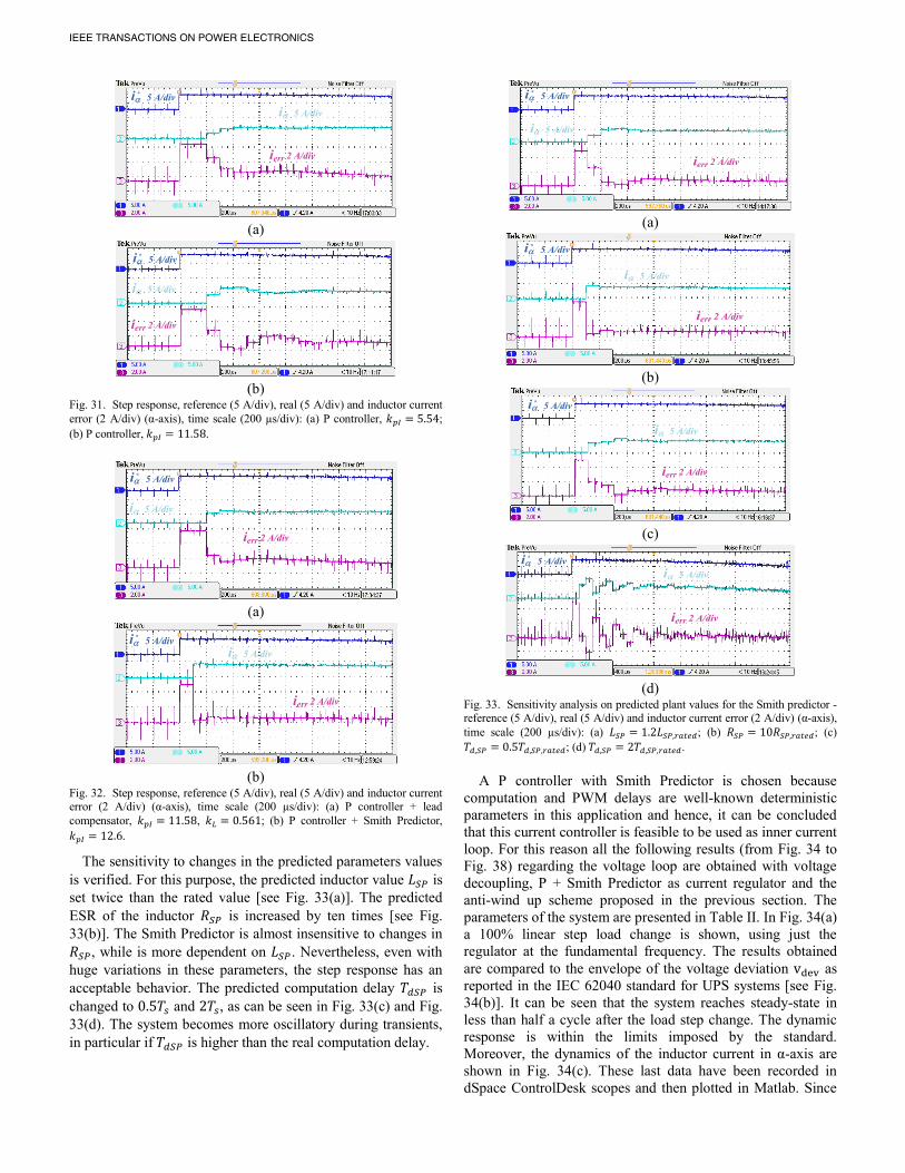
Fig. 31. Step response, reference (5 A/div), real (5 A/div) and inductor current
error (2 A/div) (α-axis), time scale (200 µs/div): (a) P controller, 𝑘𝑝𝐼 = 5.54;
(b) P controller, 𝑘𝑝𝐼 = 11.58.
5 A/divia*
ia 5 A/div
ierr 2 A/div
(a)
5 A/divia*
ia 5 A/div
ierr 2 A/div
(b)
Fig. 32. Step response, reference (5 A/div), real (5 A/div) and inductor current
error (2 A/div) (α-axis), time scale (200 µs/div): (a) P controller + lead
compensator, 𝑘𝑝𝐼 = 11.58, 𝑘𝐿 = 0.561; (b) P controller + Smith Predictor,
𝑘𝑝𝐼 = 12.6.
The sensitivity to changes in the predicted parameters values
is verified. For this purpose, the predicted inductor value 𝐿𝑆𝑃 is
set twice than the rated value [see Fig. 33(a)]. The predicted
ESR of the inductor 𝑅𝑆𝑃 is increased by ten times [see Fig.
33(b)]. The Smith Predictor is almost insensitive to changes in
𝑅𝑆𝑃, while is more dependent on 𝐿𝑆𝑃. Nevertheless, even with
huge variations in these parameters, the step response has an
acceptable behavior. The predicted computation delay 𝑇𝑑𝑆𝑃 is
changed to 0.5𝑇𝑠 and 2𝑇𝑠, as can be seen in Fig. 33(c) and Fig.
33(d). The system becomes more oscillatory during transients,
in particular if 𝑇𝑑𝑆𝑃 is higher than the real computation delay.
5 A/divia*
ia 5 A/div
ierr 2 A/div
(a)
5 A/divia*
ia 5 A/div
ierr 2 A/div
(b)
5 A/divia*
ia 5 A/div
ierr 2 A/div
(c)
5 A/divia*
ia 5 A/div
ierr 2 A/div
(d)
Fig. 33. Sensitivity analysis on predicted plant values for the Smith predictor - reference (5 A/div), real (5 A/div) and inductor current error (2 A/div) (α-axis),
time scale (200 µs/div): (a) 𝐿𝑆𝑃 = 1.2𝐿𝑆𝑃,𝑟𝑎𝑡𝑒𝑑; (b) 𝑅𝑆𝑃 = 10𝑅𝑆𝑃,𝑟𝑎𝑡𝑒𝑑; (c)
𝑇𝑑,𝑆𝑃 = 0.5𝑇𝑑,𝑆𝑃,𝑟𝑎𝑡𝑒𝑑; (d) 𝑇𝑑,𝑆𝑃 = 2𝑇𝑑,𝑆𝑃,𝑟𝑎𝑡𝑒𝑑.
A P controller with Smith Predictor is chosen because
computation and PWM delays are well-known deterministic
parameters in this application and hence, it can be concluded
that this current controller is feasible to be used as inner current
loop. For this reason all the following results (from Fig. 34 to
Fig. 38) regarding the voltage loop are obtained with voltage
decoupling, P + Smith Predictor as current regulator and the
anti-wind up scheme proposed in the previous section. The
parameters of the system are presented in Table II. In Fig. 34(a)
a 100% linear step load change is shown, using just the
regulator at the fundamental frequency. The results obtained
are compared to the envelope of the voltage deviation vdev as
reported in the IEC 62040 standard for UPS systems [see Fig.
34(b)]. It can be seen that the system reaches steady-state in
less than half a cycle after the load step change. The dynamic
response is within the limits imposed by the standard.
Moreover, the dynamics of the inductor current in α-axis are
shown in Fig. 34(c). These last data have been recorded in
dSpace ControlDesk scopes and then plotted in Matlab. Since

IEEE TRANSACTIONS ON POWER ELECTRONICS
the capacitor voltage is sinusoidal, the inductor current is
slightly distorted even in case a linear load is supplied.
va
verr
va*
(a)
0-20 20 40 8060 100 120 140Time (ms)
0
10
20
-20
-10Am
pli
tud
e (%
)
IEC 62040 – Linear Load
vdev
(b)
0-20 20 40 8060 100 120 140Time (ms)
0
4
6
-2Cu
rren
t (A
)
2
-4
-6
iα
ierr
iα *
(c) Fig. 34. Linear step load changing (0 – 100%): (a) reference (200 V/div), real
(200 V/div) and capacitor voltage error (50 V/div) (α-axis), time scale (4
ms/div); (b) Dynamic characteristics according to IEC 62040 standard for
linear loads: overvoltage (𝑣𝑑𝑒𝑣 > 0) and undervoltage (𝑣𝑑𝑒𝑣 < 0); (c)
reference, real and inductor current error (α-axis).
A diode bridge rectifier with an LC output filter supplying
a resistive load is used as nonlinear load. Its parameters are
presented in Table II. A 100% nonlinear step load change is
performed with and without the harmonic compensators (HC)
tuned at the 5th
and 7th harmonics. The results are in accordance
with the standard IEC 62040 even for linear loads, as can be
seen in Fig. 35(b) and Fig. 36(b). The correspondent inductor
current in α-axis for the test performed without HC is shown in
Fig. 35(c). A similar trend for the inductor current is achieved
with the HC activated. It is evident in Fig. 36(b) that the
benefits of using the harmonic compensators are in a lower the
steady-state error
va
verr
va*
(a)
IEC 62040 – Linear Load
IEC 62040 – Non-Linear Load
0
40
80
-80
-40Am
pli
tude
(V)
0-20 20 40 8060 100 120 140Time (ms)
vdev
(b)
Curr
ent
(A)
0-20 20 40 8060 100 120 140Time (ms)
*iα iα
ierr
8
4
0
-4
-8
(c) Fig. 35. Nonlinear step load changing (0 – 100%) without HC: (a) reference
(200 V/div), real (200 V/div) and capacitor voltage error (50 V/div) (α-axis), time scale (10 ms/div); (b) Dynamic characteristics according to IEC 62040
standard for linear and nonlinear loads: overvoltage (𝑣𝑑𝑒𝑣 > 0) and
undervoltage (𝑣𝑑𝑒𝑣 < 0); (c) reference, real and inductor current error (α-axis).
va
verr
va*
(a) IEC 62040 – Linear Load
IEC 62040 – Non-Linear Load
0
40
80
-80
-40Am
pli
tude
(V)
0-20 20 40 8060 100 120 140Time (ms)
vdev
(b) Fig. 36. Nonlinear step load changing (0 – 100%) with HC at 5th and 7th
harmonics: (a) reference (200 V/div), real (200 V/div) and capacitor voltage
error (50 V/div) (α-axis), time scale (10 ms/div); (b) Dynamic characteristics according to IEC 62040 standard for linear and nonlinear loads: overvoltage
(𝑣𝑑𝑒𝑣 > 0) and undervoltage (𝑣𝑑𝑒𝑣 < 0).
To verify the attenuation of triplen harmonics, a 100%
nonlinear unbalance (one phase open) step load change is
performed, using the harmonic compensator at the fundamental
frequency only. The response is again in the boundaries
imposed to linear loads [see Fig. 37(a)]. The FFT results in Fig.
37(b) show the mitigation of the 3rd
harmonic component by a
large extent, even with just the resonator tuned at the
fundamental frequency. These results show the benefits of
widening the bandwidth for the voltage loop, which can be

IEEE TRANSACTIONS ON POWER ELECTRONICS
achieved with the design of the inner current loop based on
Smith predictor.
IEC 62040 – Linear Load
IEC 62040 – Non-Linear Load
0
40
80
-80
-40Am
pli
tude
(V)
0-20 20 40 8060 100 120 140Time (ms)
vdev
(a)
1st
5th
7th
THDv = 5.6%
HDv5th
= 2.5%
HDv7th
= 0.7%3
rd
HDv3rd
= 4.5%
(b) Fig. 37. Unbalance nonlinear step load changing (0 – 100%): (a) Dynamic
characteristics according to IEC 62040 standard for linear and nonlinear loads:
overvoltage (vdev > 0) and undervoltage (vdev < 0) without HC; (b) FFT of
the capacitor voltage.
In order to show the performance of the anti-wind up
implementation, a saturated control action (current reference)
along with results of a step change from rated load to overload
conditions and vice versa are shown in Fig. 38(a) and Fig.
38(b). The current limiter is set to 8 A as well as the saturation
blocks in the anti-wind up scheme. It can be noted the output of
the integral is bounded because of the anti-wind up scheme
implemented.
va
iα
vInt,output
(a)
vInt,output va
iα
(b) Fig. 38. Linear step load changing (100% - 950% and viceversa) - integral
output (100 V/div), real capacitor voltage (200 V/div) and real inductor current
(5 A/div) (α-axis), time scale (20 ms/div): (a) from rated load (68 Ω) to
overload conditions (7.2 Ω); (b) from overload conditions (7.2 Ω) to rated load (68 Ω).
VII. CONCLUSIONS
Recent approaches in the control of power converters
working in standalone applications have proved that state-
feedback decoupling allows better dynamic response to be
achieved. In this context, the model derived directly in the
discrete-time domain permits a clear representation of the
limitations in dynamics introduced by computation and PWM
delays when state feedback voltage decoupling is performed.
The simulation results validate the discrete-time model
developed, which allows access to the internal states of the
system. In order to enhance the current controller dynamics, a
P controller with a lead compensator and Smith Predictor
structure are implemented and compared. The implementation
based on Smith Predictor has been shown to provide the
fastest response to changes in the reference inductor current,
allowing the current loop bandwidth to be widened while still
preserving good dynamic properties. The wider inner current
control bandwidth permits the bandwidth of the voltage loop
to be increased. A systematic design methodology based on
the Nyquist criterion allows the fundamental integral gain
value to be identified by means of a straightforward
mathematical relationship. As the dynamics of the voltage
loop are faster, an anti-wind up scheme becomes even more
important. The proposed design in the discrete-time domain of
the anti-wind up scheme based on a feedback implementation
of inverse dynamics avoids algebraic loops, which could arise
depending on the discretization method employed.
The overall design provides good performance both in
steady-state and transient conditions. More specifically, the
requirements during the transient, imposed by the UPS
standard IEC 62040, are verified according to the design
proposed for the current and voltage regulators. Moreover,
when a balanced or even unbalanced nonlinear load is
supplied, the dynamic response is within the standards
imposed to linear loads with just the compensator tuned at
fundamental frequency.
APPENDIX
In this section the derivation of the first Cross-Coupled State
Equation is provided, following the step-by-step methodology
provided in Section II. Moreover, the derivation of the transfer
function 𝑽𝐶𝛼𝛽(𝑧)/𝑰𝐿𝛼𝛽(𝑧) is provided.
Eq. (6) is derived as follows. Firstly, the Inverse Laplace
Transform applied to (3) leads to
𝑣𝑐(𝑡) = [1 −1
√1 − 𝜉2𝑒−𝜉𝜔𝑛𝑡 sin(𝜔𝑑𝑡 + 𝜙)] 𝑣𝑖(𝑡 = 0)
+𝑣𝑐(𝑡 = 0)
𝜔𝑛2
−𝜔𝑛2
√1 − 𝜉2𝑒−𝜉𝜔𝑛𝑡 sin(𝜔𝑑𝑡 − 𝜙)
+2𝜉
𝜔𝑛𝑣𝑐(𝑡 = 0)
𝜔𝑛
√1 − 𝜉2𝑒−𝜉𝜔𝑛𝑡 sin(𝜔𝑑𝑡)
+�̇�𝑐(𝑡 = 0)
𝜔𝑛2
𝜔𝑛
√1 − 𝜉2𝑒−𝜉𝜔𝑛𝑡 sin(𝜔𝑑𝑡).
(A.1)
Accordingly, the response in the next sample time is
IEEE TRANSACTIONS ON POWER ELECTRONICS
𝑣𝑐(𝑇) = [1 −1
√1 − 𝜉2𝑒−𝜉𝜔𝑛𝑇 sin(𝜔𝑑𝑇 + 𝜙)] 𝑣𝑖(𝑡 = 0)
−𝜔𝑛𝜔𝑑
𝑒−𝜉𝜔𝑛𝑡 sin(𝜔𝑑𝑇 − 𝜙)𝑣𝑐(𝑡 = 0)
+2𝜉𝜔𝑛𝜔𝑑
𝑒−𝜉𝜔𝑛𝑇 sin(𝜔𝑑𝑇)𝑣𝑐(𝑡 = 0)
+1
𝜔𝑑𝑒−𝜉𝜔𝑛𝑇 sin(𝜔𝑑𝑇)�̇�𝑐(𝑡 = 0).
(A.2)
The solution at a generic sample instant is
𝑣𝑐(𝑘𝑇) = [1 −1
√1 − 𝜉2𝑒−𝜉𝜔𝑛𝑇 sin(𝜔𝑑𝑇 + 𝜙)] 𝑣𝑖((𝑘 − 1)𝑇)
−𝜔𝑛𝜔𝑑
𝑒−𝜉𝜔𝑛𝑡 sin(𝜔𝑑𝑇 − 𝜙)𝑣𝑐((𝑘 − 1)𝑇)
+2𝜉𝜔𝑛𝜔𝑑
𝑒−𝜉𝜔𝑛𝑇 sin(𝜔𝑑𝑇)𝑣𝑐((𝑘 − 1)𝑇)
+1
𝜔𝑑𝑒−𝜉𝜔𝑛𝑇 sin(𝜔𝑑𝑇)�̇�𝑐((𝑘 − 1)𝑇).
(A.3)
This equation cannot be written in transfer function format
due to the term �̇�𝑐((𝑘 − 1)𝑇). However, being �̇�𝑐((𝑘 −
1)𝑇) =1
𝐶𝑓𝑖𝐿((𝑘 − 1)𝑇), this model with cross-coupling can
be written as
𝑣𝑐(𝑘𝑇) = [1 −1
√1 − 𝜉2𝑒−𝜉𝜔𝑛𝑇 sin(𝜔𝑑𝑇 + 𝜙)] 𝑣𝑖((𝑘 − 1)𝑇)
−𝜔𝑛𝜔𝑑
𝑒−𝜉𝜔𝑛𝑡 sin(𝜔𝑑𝑇 − 𝜙)𝑣𝑐((𝑘 − 1)𝑇)
+2𝜉𝜔𝑛𝜔𝑑
𝑒−𝜉𝜔𝑛𝑇 sin(𝜔𝑑𝑇)𝑣𝑐((𝑘 − 1)𝑇)
+1
𝐶𝑓𝜔𝑑𝑒−𝜉𝜔𝑛𝑇 sin(𝜔𝑑𝑇)𝑖𝐿((𝑘 − 1)𝑇).
(A.4)
By substituting for the z operator in the discrete-time domain
and by transforming to the αβ stationary reference frame leads
to
𝑽𝑐𝛼𝛽(𝑧) [1 +𝜔𝑛𝜔𝑑
𝑒−𝜉𝜔𝑛𝑇 sin(𝜔𝑑𝑇 − 𝜙)𝑧−1 −
2𝜉𝜔𝑛𝜔𝑑
𝑒−𝜉𝜔𝑛𝑇sin(𝜔𝑑𝑇)𝑧−1]
= [1 −𝜔𝑛𝜔𝑑
𝑒−𝜉𝜔𝑛𝑇 sin(𝜔𝑑𝑇 + 𝜙)] 𝑽𝑖𝛼𝛽(𝑧)𝑧−1
+1
𝐶𝑓𝜔𝑑𝑒−𝜉𝜔𝑛𝑇 sin(𝜔𝑑𝑇) 𝑰𝐿𝛼𝛽(𝑧).
(A.5)
A similar mathematical development can be performed to
derive (7), starting from (4). Solving the coupling equations
(6) and (7), yields to the independent TF
𝑽𝑐𝛼𝛽(𝑧)
𝑽𝑖𝛼𝛽(𝑧)=
𝑎1𝑧−1 + 𝑎2𝑧
−2
1 + 𝑏1𝑧−1 + 𝑏2𝑧
−2(A.6)
where
𝑎1 = 1 −𝜉𝜔𝑛𝜔𝑑
𝑒−𝜉𝜔𝑛𝑇 sin(𝜔𝑑𝑇) − 𝑒−𝜉𝜔𝑛𝑇 cos(𝜔𝑑𝑇)
𝑎2 =𝜉𝜔𝑛𝜔𝑑
𝑒−𝜉𝜔𝑛𝑇 sin(𝜔𝑑𝑇) − 𝑒−𝜉𝜔𝑛𝑇 cos(𝜔𝑑𝑇) + 𝑒
−2𝜉𝜔𝑛𝑇
𝑏1 = −2𝑒−𝜉𝜔𝑛𝑇 cos(𝜔𝑑𝑇); 𝑏2 = 𝑒
−2𝜉𝜔𝑛𝑇
Similarly, starting from (6) we can achieve the transfer
function 𝑰𝐿𝛼𝛽(𝑧)/𝑽𝑖𝛼𝛽(𝑧) already including the output voltage
feedback, i.e. 𝑽𝑐𝛼𝛽(𝑧)
𝑰𝐿𝛼𝛽(𝑧)
𝑽𝑖𝛼𝛽(𝑧)=
[𝐶𝑓𝜔𝑛2
𝜔𝑑𝑒−𝜉𝜔𝑛𝑇 sin(𝜔𝑑𝑇)] (𝑧
−1 − 𝑧−2)
1 − 2𝑒−𝜉𝜔𝑛𝑇 cos(𝜔𝑑𝑇) 𝑧−1 + 𝑒−2𝜉𝜔𝑛𝑇𝑧−2
. (A.7)
The derivation of (A.7) is necessary to obtain the transfer
function 𝑽𝑐𝛼𝛽(𝑧)/𝑰𝐿𝛼𝛽(𝑧). In fact, by considering (A.6) and
(A.7), the relationship between 𝑰𝐿𝛼𝛽(𝑧) and 𝑽𝑐𝛼𝛽(𝑧) can be
derived as 𝑽𝑐𝛼𝛽(𝑧)
𝑰𝐿𝛼𝛽(𝑧)=𝑽𝑐𝛼𝛽(𝑧)
𝑽𝑖𝛼𝛽(𝑧)⋅𝑽𝑖𝛼𝛽(𝑧)
𝑰𝐿𝛼𝛽(𝑧). (A.8)
REFERENCES
[1] T. M. Rowan and R. J. Kerkman, "A New Synchronous Current
Regulator and an Analysis of Current-Regulated Pwm Inverters," IEEE Trans. Ind. Appl., vol. IA-22, no. 4, pp. 678-690, Jul./Aug.
1986.
[2] M. P. Kazmierkowski and L. Malesani, "Current control techniques for three-phase voltage-source PWM converters: A
survey," IEEE Trans. Ind. Electron., vol. 45, no. 5, pp. 691-703,
May 1998. [3] R. Teodorescu, M. Liserre, and P. Rodriguez, Grid Converters for
Photovoltaic and Wind Power Systems. New York, NY, USA:
Wiley-IEEE Press, 2011. [4] F. de Bosio, L. A. de S. Ribeiro, F. D. Freijedo, M. Pastorelli, and
J. M. Guerrero, “Effect of state feedback coupling and system
delays on the transient performance of stand-alone VSI with LC output filter”, IEEE Trans. Ind. Electron., vol. 63, no. 8, Aug.
2016.
[5] S. Buso and P. Mattavelli, Digital Control in Power Electronics,
1st ed., San Rafael, CA, USA: Morgan & Claypool, 2006.
[6] D. M. Van De Sype, K. De Gussemé, F. M. L. L. De Belie, A. P.
Van den Bossche, and J. A. Melkebeek, "Small-Signal z -Domain Analysis of Digitally Controlled Converters," IEEE Trans. Power
Electron., vol. 21, no. 2, pp. 470-478, Mar. 2006. [7] A. G. Yepes, F. D. Freijedo, J. Doval-Gandoy, Ó. L. J. Malvar, and
P. Fernandez-Comesaña, "Effects of Discretization Methods on the
Performance of Resonant Controllers," IEEE Trans. Power Electron., vol. 25, no. 7, pp. 1692-1712, Jul. 2010.
[8] Y. Ito and S. Kawauchi, "Microprocessor based robust digital
control for UPS with three-phase PWM inverter," IEEE Trans. Power Electron., vol. 10, no. 2, pp. 196-204, Feb. 1995.
[9] D. Maksimovic, R. Zane, "Small-Signal Discrete-Time Modeling
of Digitally Controlled PWM Converters," IEEE Trans. Power Electron., vol. 22, no.6, pp. 2552-2556, Nov. 2007.
[10] R. D. Middlebrook, “Predicting modulator phase lag in PWM
converter feedback loops,” in Proc. of the Advances in Switched mode Power Conversion, paper H-4, pp. 245–250, 1981.
[11] L. Corradini, D. Maksimovic, P. Mattavelli, and R. Zane, “Digital
Control of High-Frequency Switched-Mode Power Converters,” 1st ed., New York, United States: John Wiley & Sons, 2015.
[12] F. D. Freijedo, A. Vidal, A. G. Yepes, J. M. Guerrero, O. Lopez, J.
Malvar, and Jesús Doval-Gandoy, "Tuning of Synchronous-Frame PI Current Controllers in Grid-Connected Converters Operating at
a Low Sampling Rate by MIMO Root Locus," IEEE Trans. Ind.
Electron., vol. 62, no. 8, pp. 5006-5017, Aug. 2015. [13] Y. Shi, Y. Wang, and R. D. Lorenz, " Low-Switching-Frequency
Flux Observer and Torque Model of Deadbeat–Direct Torque and
Flux Control on Induction Machine Drives," IEEE Trans. Ind. Appl., vol. 51, no. 3, pp. 2255-2267, May/Jun. 2015.
[14] M. Hinkkanen, H. Awan, Z. Qu, T. Tuovinen, and F. Briz,
"Current Control for Synchronous Motor Drives: Direct Discrete-Time Pole-Placement Design," IEEE Trans. Ind. Appl., vol. 52, no.
2, pp. 1530-1541, Mar./Apr. 2016.
[15] B. P. McGrath, S. G. Parker, and D. G. Holmes, "High performance stationary frame AC current regulation incorporating
transport delay compensation," EPE Journal, vol. 22, no. 4, pp. 17-
24, Dec. 2012. [16] H. Kum-Kang and R. D. Lorenz, "Discrete-time domain modeling
and design for AC Machine Current Regulation," in Conf. Rec.
IEEE IAS Annu. Meeting, New Orleans, LA, USA, 2007, pp. 2066-2073.
[17] K. Hongrae, M. W. Degner, J. M. Guerrero, F. Briz, and R. D.
Lorenz, "Discrete-Time Current Regulator Design for AC machine drives," IEEE Trans. Ind. Appl., vol. 46, no. 4, pp. 1425-1435,
Jul./Aug. 2010.
[18] R. D. Lorenz, D. B. Lawson, and M. O. Lucas, “Synthesis of State Variable Controllers for Industrial Servo Drives,” Research Report
86 – 8, WEMPEC – University of Wisconsin, May 1986.
[19] R. D. Lorenz, T. A. Lipo, and D. W. Novotny, “Motion Control with induction motor drives,” Proc. of the IEEE, vol. 82, no. 8, pp.
1215 – 1240, Mar. 1994.
[20] E. de C. Gomes, L. A. de S. Ribeiro, J. V. M. Caracas, S. Y. C. Catunda, and R. D. Lorenz, “State Space Decoupling Control
Design Methodology for Switching Converters,” in Conf. Rec. ECCE, pp. 4151 – 4158, Sept. 2010..

IEEE TRANSACTIONS ON POWER ELECTRONICS
[21] P. C. Loh, M. J. Newman, D. N. Zmood, and D. G. Holmes, “A
Comparative Analysis of Multiloop Voltage Regulation Strategies
for Single and Three-Phase UPS Systems,” IEEE Trans. on Power Electron., vol. 18, no. 5, pp. 1176 – 1185, Sept. 2003.
[22] P. Mattavelli, "An improved deadbeat control for UPS using
disturbance observers," IEEE Trans. Ind. Electron., vol. 52, no. 1, pp. 206-212, Feb. 2005.
[23] D. G. Holmes and T. A. Lipo, Pulse Width Modulation for Power
Converters: Principles and Practice. New York, NY, USA: Wiley-IEEE Press, 2003.
[24] P. Mattavelli, F. Polo, F. D. Lago, and S. Saggini, "Analysis of
Control-Delay Reduction for the Improvement of UPS Voltage-Loop Bandwidth," IEEE Trans. Ind. Electron., vol. 55, no. 8, pp.
2903-2911, Aug. 2008.
[25] M. J. Ryan, W. E. Brumsickle, and R. D. Lorenz, "Control topology options for single-phase UPS inverters," IEEE Trans. Ind.
Appl., vol. 33, no. 2, pp. 493-501, Mar./Apr. 1997. [26] K. J. Aström and T. Hägglung, PID Controllers: Theory,
Designing, and Tuning, 2nd ed., Research Triangle Park, NC,
USA: Instrum. Soc. of Amer., 2006. [27] F. Briz, M. W. Degner, and R. D. Lorenz, "Analysis and Design of
Current Regulators Using Complex Vectors," IEEE Trans. Ind.
Appl., vol. 36, no. 3, pp. 817-825, May/Jun. 2000. [28] G. C. Goodwin, S. F. Graebe, and M. E. Salgado, Control System
Design, 1st ed., Valparaíso, Chile: Pearson, 2000.
[29] P. C. Loh and D. G. Holmes, "Analysis of Multiloop Control Strategies for LC-CL-CLC Filtered Voltage Source and Current
Source Inverters," IEEE Trans. Ind. Appl., vol. 41, no. 2, pp. 644-
654, Mar./Apr. 2005. [30] F. G. Shinskey, B. G. Liptak, R. Bars, and J. Hetthéssy, "Control
Systems - Cascade Loops," in Instrument Engineers' Handbook:
Process Control and Optimization., 4th ed., vol. 2, Boca Raton, FL:CRC Press, , 2006.
[31] A. G. Yepes, F. D. Freijedo, O. López, and J. Doval-Gandoy,
"Analysis and Design of Resonant Current Controllers for Voltage-Source Converters by Means of Nyquist Diagrams and Sensitivity
Function," IEEE Trans. Ind. Electron., vol. 58, no. 11, pp. 5231-
5250, Nov. 2011. [32] A. Vidal, F. D. Freijedo, A. G. Yepes, P. Fernández-Comesaña, J.
Malvar, O. López, and J. Doval-Gandoy, "Assessment and
Optimization of the Transient Response of Proportional-Resonant Current Controllers for Distributed Power Generation Systems,"
IEEE Trans. Ind. Electron., vol. 60, no. 4, pp. 1367-1383, Apr.
2013. [33] G. C. Goodwin, S. F. Graebe, and W. S. Levine, "Internal model
control of linear systems with saturating actuators," in Proc. ECC,
Groningen, NL, 1993, pp. 1072-1077.
Federico de Bosio (S’14) was born in Torino,
Italy, in 1989. He received the B.Sc. and M.Sc. degrees from the Politecnico di Torino, Turin,
Italy, in 2011 and 2013, respectively.
Since 2014 he is pursuing the Ph.D. degree in
Electrical, Electronics and Telecommunications
Engineering at the Politecnico di Torino.
In 2015 he was a visiting Ph.D. researcher at the Department of Energy Technology of Aalborg
University, Denmark, working on control of
power converters for islanded microgrids/UPS systems. His main research interests include
control of power converters, energy storage systems and optimal energy
management.
Luiz A. de S. Ribeiro (M’98) received the M.Sc.
and Ph.D. degrees from the Federal University of Paraiba, Campina Grande, Brazil, in 1995 and
1998, respectively. During the period 1996-1998
and 2004-2004, he was a visiting scholar and post-doctor at the University of Wisconsin,
Madison, WI, USA, working on parameter estimation of induction machines and sensorless
control of AC machines.
In 2015 he was a research guest at Aalborg University. Since 2008, he has been an Associate
Professor with the Federal University of Maranhão, São Luís, Brazil. His main
areas of research interest include electric machines and drives, power
electronics, and renewable energy.
Francisco D. Freijedo (M’07) received the M.Sc.
degree in Physics from the University of Santiago
de Compostela, Santiago de Compostela, Spain, in 2002 and the Ph.D. degree from the University of
Vigo, Vigo, Spain, in 2009.
From 2005 to 2011, he was a Lecturer with the Department of Electronics Technology of the
University of Vigo.
From 2011 to 2014, he worked in Gamesa Innovation and Technology as a power electronics
control engineer for renewable energy
applications. From 2014 to 2016 he was a Postdoctoral
researcher at the Department of Energy Technology of Aalborg University.
Since 2016, he is a Postdoctoral Researcher at the Power Electronics Lab of the École Polytechnique Fédérale de Lausanne.
His main research interest is focused on power conversion technologies.
Michele Pastorelli (M’05) was born in Novara,
Italy, in1962. He received the Laurea and Ph.D. degrees in electrical engineering from the
Politecnico di Torino, Turin, Italy, in 1987 and
1992, respectively. Since 1988, he has been with the Politecnico di
Torino, where he has been a Full Professor of
electrical machines and drives since November 2006. He has authored about 100 papers published
in technical journals and conference proceedings. His scientific activity concerns power electronics, high performance servo
drives, and energetic behaviors of electrical machines.
His main research interests include synchronous drives for both industrial and commercial residential applications. He has been involved as a Consultant in
research contracts with foreign and Italian industries. He has been in charge of
several national research projects funded by the Italian Research Ministry in the field of ac drives.
Josep M. Guerrero (S’01-M’04-SM’08-FM’15)
received the B.Sc. degree in telecommunications
engineering, the M.Sc. degree in electronics engineering, and the Ph.D. degree in power
electronics from the Technical University of
Catalonia, Barcelona, in 2000 and 2003, respectively. Since 2011, he has been a Full
Professor with the Department of Energy
Technology, Aalborg University, Denmark, where he is responsible for the Microgrid Research
Program. From 2012 he is a guest Professor at the Chinese Academy of
Science and the Nanjing University of Aeronautics and Astronautics; and
from 2014 he is chair Professor in Shandong University.
His research interests is oriented to different microgrid aspects, including
power electronics, distributed energy-storage systems, hierarchical and
cooperative control, energy management systems, and optimization of
microgrids and islanded minigrids. In 2014 he was awarded by Thomson
Reuters as ISI Highly Cited Researcher, and in 2015 same year he was
elevated as IEEE Fellow for contributions to “distributed power systems
and microgrids”.
www.microgrids.et.aau.dk