Embed Size (px)
Citation preview
Aalborg Universitet
A Novel 3D Thermal Impedance Model for High Power Modules Considering Multi-layerThermal Coupling and Different Heating/Cooling Conditions
Bahman, Amir Sajjad; Ma, Ke; Blaabjerg, Frede
Published in:Proceedings of the 2015 IEEE Applied Power Electronics Conference and Exposition (APEC)
DOI (link to publication from Publisher):10.1109/APEC.2015.7104501
Publication date:2015
Document VersionAccepted author manuscript, peer reviewed version
Link to publication from Aalborg University
Citation for published version (APA):Bahman, A. S., Ma, K., & Blaabjerg, F. (2015). A Novel 3D Thermal Impedance Model for High Power ModulesConsidering Multi-layer Thermal Coupling and Different Heating/Cooling Conditions. In Proceedings of the 2015IEEE Applied Power Electronics Conference and Exposition (APEC) (pp. 1209-1215). IEEE Press. I E E EApplied Power Electronics Conference and Exposition. Conference Proceedingshttps://doi.org/10.1109/APEC.2015.7104501
General rightsCopyright and moral rights for the publications made accessible in the public portal are retained by the authors and/or other copyright ownersand it is a condition of accessing publications that users recognise and abide by the legal requirements associated with these rights.
- Users may download and print one copy of any publication from the public portal for the purpose of private study or research. - You may not further distribute the material or use it for any profit-making activity or commercial gain - You may freely distribute the URL identifying the publication in the public portal -
Take down policyIf you believe that this document breaches copyright please contact us at [email protected] providing details, and we will remove access tothe work immediately and investigate your claim.

A Novel 3D Thermal Impedance Model for High Power Modules Considering Multi-layer Thermal Coupling and
Different Heating/Cooling Conditions
Amir Sajjad Bahman, IEEE Student Member, Ke Ma, IEEE Member, Frede Blaabjerg, IEEE Fellow Center of Reliable Power Electronics (CORPE),
Department of Energy Technology Aalborg University
Pontoppidanstraede 101, Aalborg DK-9220, Denmark [email protected], [email protected], [email protected]
Abstract— Thermal management of power electronic devices is essential for reliable performance especially at high power levels. One of the most important activities in the thermal management and reliability improvement is acquiring the temperature information in critical points of the power module. However accurate temperature estimation either vertically or horizontally inside the power devices is still hard to identify. This paper investigates the thermal behavior of high power module in various operating conditions by means of Finite Element Method (FEM). A novel 3D thermal impedance network considering the multi-layer thermal coupling among chips is proposed. The impacts to the thermal impedance by various cooling and heating conditions are also studied. It is concluded that the heating and cooling conditions will have influence on the junction to case thermal impedances and need to be carefully considered in the thermal modelling. The proposed 3D thermal impedance network and the extraction procedure are verified in a circuit simulator and shows to be much faster with the same accuracy compared to FEM simulation. This network can be used for life-time estimation of IGBT module considering the whole converter system and more realistic loading conditions of the device.
Keywords—Thermal impedance; finite element method; thermal coupling; heating/cooling conditions; reliability.
I. INTRODUCTION In recent years power electronic devices have found wide
applications in many industries like renewable energy systems, motor drives and automation [1], [2]. Since industries demand for both higher power densities and higher power levels, more power losses will be dissipated and a large amount of heat will be generated in the power electronic devices [3], [4]. As one of the key components in power electronic systems, IGBT modules are exposed to wear-out failures like bond-wire lift-off or solder cracking due to adverse thermal cycling caused by heat dissipation[5], [6]. In addition, semiconductor chips inside the IGBT modules may lead to failures, if the maximum allowed junction temperatures are violated [7]. Therefore, information regarding the temperatures in critical points inside the power module is important to ensure a reliable design of converter [8], [9].
Today, many methods are applied to identify the detailed junction temperatures inside the power modules. The
experimental methods are based on using IR camera, thermocouples and voltage/current sensors, which need direct access into the devices and proper measurement equipment [10]-[12]. Besides, there are other methods based on indirect estimation of junction temperature by means of information given in datasheet [13], [14]. However, these methods just give a rough estimation in respect to the average junction temperature on chip and detailed thermal distribution either on the surface of chips and different layers inside the IGBT modules cannot be covered. For more accurate identification of temperatures of IGBT module and thereby ensure a reliable design of converter, more advanced methods must be used by considering the physical properties and geometries inside the power devices [15].
One of the most straight forward methods used in calculation of temperatures inside a power module is by means of using a thermal impedance model. Knowing the power dissipation inside the power module, accurate temperatures in different layers can be found by using transient thermal impedance networks inside the IGBT module. However, the thermal impedance is not an independent value and it is exposed to changes by several internal and external factors. The internal factors are those which relate to power module structure, e.g. geometries of different layers and materials used in the device [16]. IGBT and diode locations on the substrate of the IGBT module are one of the internal factors, which influences on the coupling thermal impedances between the chips [17]. On the other hand, the external factors are those which relate to boundary and operating conditions of the power module, e.g. ambient temperature, loading conditions and cooling system.
Finding an accurate thermal model based on the thermal impedances in different layers of the device which considers internal and external factors is important in order to calculate accurate temperatures. This paper proposes a 3D thermal network including different locations on the chip surfaces and critical layers of power module based on FEM simulations. This thermal network considers geometries and thermal characteristics of materials that can be used by any circuit simulator for much faster temperature and life-time estimation compared to the FEM approach without compromising the accuracy. The model structure and operating conditions are

explained based on real operating conditions of a three-phase DC-AC converter. Various loss and cooling conditions are also tested to define the applicable ranges of the proposed thermal model. In the last section, the presented thermal network is verified by comparing FEM simulations with simulations using a circuit simulator for two different power loss profiles and cooling systems.
II. MODELLING PROCESS OF IGBT MODULE IN FEM The target power module is loaded with a three-phase DC-
AC voltage source converter, which is shown in Fig. 1. The converter specifications are shown in Table I as a case study. The used power module composed of 6 half-bridge converters mounted on 6 DCBs (Direct Copper Bonded) and can operate for the load currents up to 1 kA with blocking voltage of 1.7 kV. The IGBT module is simulated in ANSYS Icepak to find the temperature profile of the system. The schematic view of the IGBT module is shown in Fig. 2. For simplification of the model and reduction of simulation time, bond-wires are ignored in the model. It is assumed that IGBT module is adiabatic from the top surface, so heat is generated in the junction area of the chips and propagates through lower layers of IGBT module and dissipated in the heat exchanger.
The geometries and the material properties of the different layers are supplied by the IGBT module manufacturer. The thermal properties of materials are listed in Table II. It can be seen in Table II that some materials are set with thermal conductivities as temperature dependent based on [19]. The main reason is that different materials used in the IGBT
module show different behavior at various temperatures, especially Silicon and Copper. So, for more accurate thermal characterization of the IGBT module in different loading conditions, temperature dependent thermal conductivities are needed to be defined.
As simple boundary conditions of the modeled IGBT module, the ambient temperature is set to 80 , a loss profile is injected to the IGBT and diode chips, and the base-plate is placed on a hot plate with a constant temperature of 80 . The loss profile is obtained by simulation of the converter shown in Fig. 1 in a circuit simulator like PLECS and the loss profile is shown in Fig. 3. The ambient temperature is a factor that has a slight influence on the thermal behavior of the IGBT module, but it is not in the scope of this paper. The loading conditions which generate different loss profiles and cooling conditions will be investigated in IV. In addition, as discussed in the introduction, most of the wear-out failures inside the IGBT
TABLE II. IGBT MODULE MATERIAL THERMAL PROPERTIES
Material Density / Specific heat / · Conductivity / ·
Silicon in chip 2330 705
Temp. 0.0
100.0 200.0
Cond. 168.0 112.0 82.0
Copper 8954 384
Temp. 0.0
100.0 200.0
Cond. 401.0 391.0 389.0
Al2O3 in DCB 3890 880 35
SnAgCu in Solder 7370 220 57
Fig. 1. Two-level voltage source DC-AC converter (2L-VSC).
Fig. 2. Graphical view of high power IGBT module developed in
ANSYS Icepak.
TABLE I. PARAMETERS OF THE POWER CONVERTER SHOWN IN FIG. 1
Rated output active power Po 250 kW Output power factor PF 1.0 DC bus voltage Vdc 1050 VDC *Rated primary side voltage Vp 690 V rms Rated load current Iload 209 A rms Fundamental frequency fo 50 Hz Switching frequency fc 2 kHz
Filter inductance Lf 1.2 mH (0.2 p.u.)
IGBT module 1700V/1000A
* Line-to-line voltage in the primary windings of transformer.
Fig. 3. Average power losses in the IGBT module calculated by
PLECS for 25 cycles.
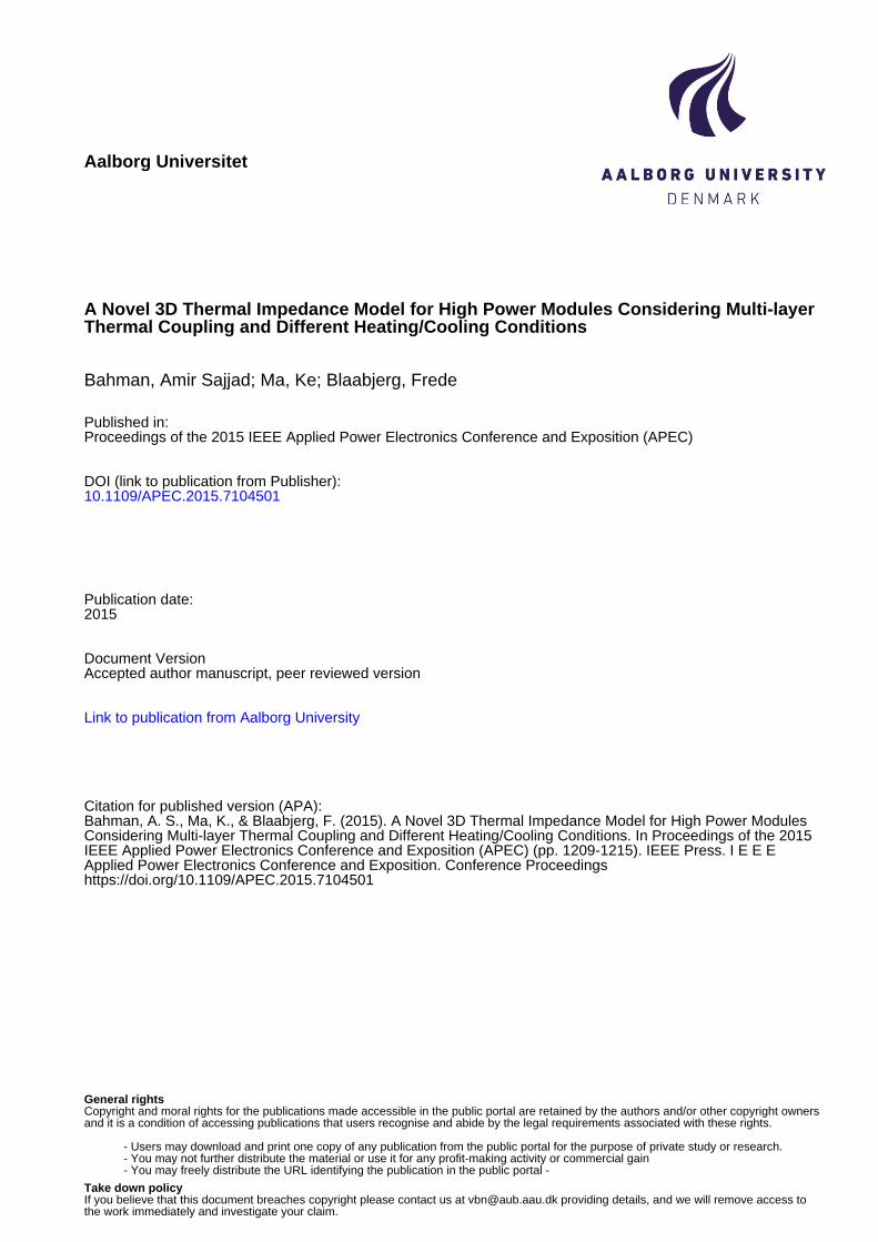
power module occur on the interconnection of the bond-wires to the Silicon chips and in the soldering layers. So, the critical points are set to the junction layer on the Silicon chips and two solder layers beneath the chips and solder layer beneath the DCB. These critical points are shown in Fig. 4.
In order to achieve the most accurate results and to save the simulation time a multi-level meshing process is executed in the FEM simulation. Multi-level meshing means that for the critical layers (junction and solder layers), finer meshing is processed rather than other layers like the base-plate and DCB. FEM simulations are run in transient mode for around 0.5 s. Within this time the average temperatures of the chips are entering into steady-state. The steady-state internal temperature profile of the IGBT module is shown in Fig. 5 for the case when the upper IGBT chips are conducting (like T1). It can be seen that the temperature is not symmetrically distributed over the surface of IGBT/Diode chips and there are mutual temperature rises between the chips. The reason comes from the thermal coupling effects between the heat sources which are junction areas in the chips. So, it can be concluded that the temperature rise on each chip is originated from self-heating and thermal coupling effects from the other chips. The thermal coupling effects are a function of power loss amounts on the chips and the distance between the chips [18]. In the IGBT module under study, the thermal coupling between the different DCB cells and between the IGBT/diode pairs are negligible compared to individual IGBT and diode in a pair. This is due to the more distance between the cells and pairs rather than distance between IGBT and diode chips.
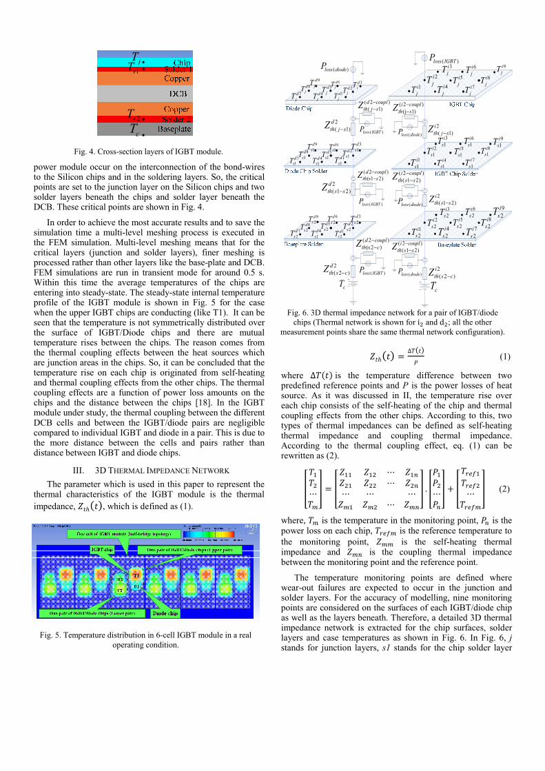
III. 3D THERMAL IMPEDANCE NETWORK The parameter which is used in this paper to represent the
thermal characteristics of the IGBT module is the thermal impedance, , which is defined as (1).
∆
(1)
where ∆ is the temperature difference between two predefined reference points and P is the power losses of heat source. As it was discussed in II, the temperature rise over each chip consists of the self-heating of the chip and thermal coupling effects from the other chips. According to this, two types of thermal impedances can be defined as self-heating thermal impedance and coupling thermal impedance. According to the thermal coupling effect, eq. (1) can be rewritten as (2).
. (2)
where, is the temperature in the monitoring point, is the power loss on each chip, is the reference temperature to the monitoring point, is the self-heating thermal impedance and is the coupling thermal impedance between the monitoring point and the reference point.
The temperature monitoring points are defined where wear-out failures are expected to occur in the junction and solder layers. For the accuracy of modelling, nine monitoring points are considered on the surfaces of each IGBT/diode chip as well as the layers beneath. Therefore, a detailed 3D thermal impedance network is extracted for the chip surfaces, solder layers and case temperatures as shown in Fig. 6. In Fig. 6, j stands for junction layers, s1 stands for the chip solder layer
jT1sT
2sTcT
Fig. 4. Cross-section layers of IGBT module.
2( 2 )
dth s cZ −
2( 1)
ith j sZ −
2( 1 2)
ith s sZ −
2( 2 )
ith s cZ −
2( 1)
dth j sZ −
2( 1 2)
dth s sZ −
cTcT
1ijT
2ijT
3ijT
5ijT
51i
sT
52i
sT
31i
sT
32i
sT
21i
sT
22i
sT
11i
sT
12i
sT
1djT
11d
sT
12d
sT
2djT
21d
sT
22d
sT
3djT
31d
sT
32d
sT
51d
sT
52d
sT
( )loss diodeP ( )loss IGBTP
5djT8d
jT
81d
sT
82d
sT
4ijT
6ijT
7ijT
8ijT
9ijT
42i
sT
62i
sT
72i
sT82i
sT92i
sT
41i
sT
61i
sT
71i
sT
81i
sT9
1i
sT
( 2 )( 1)
d couplth j sZ −
−
( )loss IGBTP
4djT
6djT
7djT
9djT
41d
sT
62d
sT7
2d
sT
92d
sT
( 2 )(s1 2)
d couplth sZ −
−
( )loss IGBTP
( 2 )(s2 )
d couplth cZ −
−
( )loss IGBTP
41d
sT
61d
sT7
1d
sT
91d
sT
( 2 )(j 1)
i couplth sZ −
−
( 2 )( 1 2)
i couplth s sZ −
−
( 2 )( 1 2)
i couplth s sZ −
−
( )loss diodeP
( )loss diodeP
( )loss diodeP
Fig. 6. 3D thermal impedance network for a pair of IGBT/diode chips (Thermal network is shown for i and d ; all the other
measurement points share the same thermal network configuration).
Fig. 5. Temperature distribution in 6-cell IGBT module in a real
operating condition.
and s2 stands for DCB solder layer. and are thermal impedances of monitoring point m between layer a and layer b for both IGBT chip and diode chip respectively. and means coupling thermal impedance of monitoring point m between layer a and layer b for the IGBT chip and diode chip respectively.
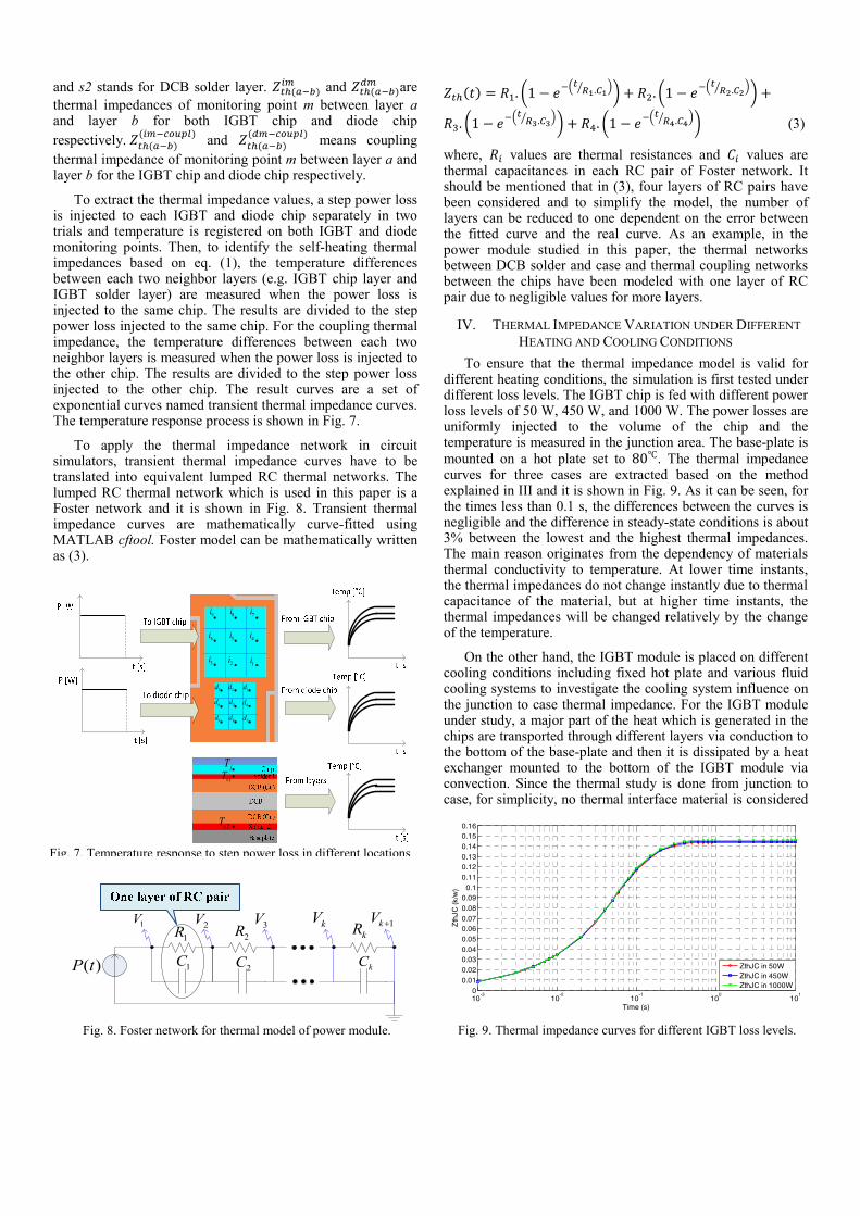
To extract the thermal impedance values, a step power loss is injected to each IGBT and diode chip separately in two trials and temperature is registered on both IGBT and diode monitoring points. Then, to identify the self-heating thermal impedances based on eq. (1), the temperature differences between each two neighbor layers (e.g. IGBT chip layer and IGBT solder layer) are measured when the power loss is injected to the same chip. The results are divided to the step power loss injected to the same chip. For the coupling thermal impedance, the temperature differences between each two neighbor layers is measured when the power loss is injected to the other chip. The results are divided to the step power loss injected to the other chip. The result curves are a set of exponential curves named transient thermal impedance curves. The temperature response process is shown in Fig. 7.
To apply the thermal impedance network in circuit simulators, transient thermal impedance curves have to be translated into equivalent lumped RC thermal networks. The lumped RC thermal network which is used in this paper is a Foster network and it is shown in Fig. 8. Transient thermal impedance curves are mathematically curve-fitted using MATLAB cftool. Foster model can be mathematically written as (3).
. 1 . . 1 .. 1 . . 1 . (3)
where, values are thermal resistances and values are thermal capacitances in each RC pair of Foster network. It should be mentioned that in (3), four layers of RC pairs have been considered and to simplify the model, the number of layers can be reduced to one dependent on the error between the fitted curve and the real curve. As an example, in the power module studied in this paper, the thermal networks between DCB solder and case and thermal coupling networks between the chips have been modeled with one layer of RC pair due to negligible values for more layers.
IV. THERMAL IMPEDANCE VARIATION UNDER DIFFERENT HEATING AND COOLING CONDITIONS
To ensure that the thermal impedance model is valid for different heating conditions, the simulation is first tested under different loss levels. The IGBT chip is fed with different power loss levels of 50 W, 450 W, and 1000 W. The power losses are uniformly injected to the volume of the chip and the temperature is measured in the junction area. The base-plate is mounted on a hot plate set to 80 . The thermal impedance curves for three cases are extracted based on the method explained in III and it is shown in Fig. 9. As it can be seen, for the times less than 0.1 s, the differences between the curves is negligible and the difference in steady-state conditions is about 3% between the lowest and the highest thermal impedances. The main reason originates from the dependency of materials thermal conductivity to temperature. At lower time instants, the thermal impedances do not change instantly due to thermal capacitance of the material, but at higher time instants, the thermal impedances will be changed relatively by the change of the temperature.
On the other hand, the IGBT module is placed on different cooling conditions including fixed hot plate and various fluid cooling systems to investigate the cooling system influence on the junction to case thermal impedance. For the IGBT module under study, a major part of the heat which is generated in the chips are transported through different layers via conduction to the bottom of the base-plate and then it is dissipated by a heat exchanger mounted to the bottom of the IGBT module via convection. Since the thermal study is done from junction to case, for simplicity, no thermal interface material is considered
1i2i3i
4i5i6i
7i8i9i
1d2d3d
4d5d6d
7d8d9d
jT1sT
2sT
Fig. 7. Temperature response to step power loss in different locations
1R 2R kR
1C 2C kC( )P t
1V 2V 3V kV 1kV +
Fig. 8. Foster network for thermal model of power module.
Fig. 9. Thermal impedance curves for different IGBT loss levels.
10-3
10-2
10-1
100
101
00.010.020.030.040.050.060.070.080.09
0.10.110.120.130.140.150.16
Time (s)
Zth
JC (k
/w)
ZthJC in 50WZthJC in 450WZthJC in 1000W
between the IGBT module and heat exchanger. To model the hot plate, a heat exchanger is set as constant temperatures of 20 , 50 and 100 .
In addition, to model the fluid cooling systems, different cooling mechanisms are considered in the heat exchanger. For each cooling conditions, the heat transfer coefficient, h, of the related mechanism is defined as a thick wall at the bottom of the power module. Heat transfer coefficient is a measure of the amount of heat transferred by convection between a solid and a fluid [19]. The equivalent heat transfer coefficients for different cooling mechanisms are noted in [19]. The heat transfer coefficient can vary from 10 / · for natural convection systems to 10 / · for phase change cooling systems. Using equivalent heat transfer coefficient instead of real cooling mechanisms will simplify the model and meshing process and reduce the simulation time. The thermal resistance
(static case of thermal impedance) can be calculated based on the heat transfer coefficient definition:
1· (4)
where h is the heat transfer coefficient and A is the effective area of heat exchanger for the heat dissipation. As an example, four levels of forced convection water cooling systems from 1000 / · to 20000 / · , are set for the heat exchanger. The FEM results are shown in Fig. 10. As it is observed, with higher heat transfer coefficients the thermal impedance from junction to case decreases especially in the transient times. The reason is that with a higher heat transfer coefficient, heat flux in the IGBT module is more localized beneath the IGBT and diode chips (as heat sources) that leads to smaller heat spreading specially in the heat spreader (or base-plate). This will reduce the effectiveness of the base-plate area in spreading the heat dissipation; so, temperature rise from junction to case will be increased and the thermal resistance will be increased in turn. Similarly, with a lower heat transfer coefficient, the heat flux is spread in a larger area of the base-plate that will increase the effectiveness of the base-plate thickness; so, the temperature rise from junction to case will be decreased and as a result the thermal resistance will be decreased in turn. A fixed temperature on the back side of the power module corresponds to an infinity heat transfer coefficient that again results in a very low heat spreading and higher thermal resistance.
The thermal network model presented in this paper is extracted based on the fixed temperature cooling condition. It is due to the fact that thermal resistance curves do not show much variation especially in the transient time instances. Of course the thermal network component values can be extracted for the other cooling mechanisms with the same procedure given in III and the corresponding thermal impedance values can be updated in Fig. 6.
V. MODEL VERIFICATION In this section, the 3D thermal impedance network
presented in III will be implemented in a circuit simulator, PLECS, and verified by commercial FEM software, ANSYS Icepak. The loss profile given in Fig. 3 is injected to the IGBT and diode chips and temperatures are measured in the IGBT and DCB solder layers. Calculation of multi-layer temperature beneath the chips is one of the contributions of this thermal model which cannot be done by manufacturer datasheet or experimental setups due to inaccessible temperature measurement points. The temperature results for the three measurement points of , and (as previously described in Fig. 7) are shown in Fig. 11.a and Fig. 11.b. The simulation results in both cases are well tracking each other with a maximum error of 1.3 % at temperature monitoring point _ . The simulation time for the proposed 3D thermal model to obtain steady-state average temperature is around 15 seconds with Intel i7 3740QM, RAM 8GB system and for the FEM model it is around 12 minutes with Intel E5-2650, RAM 64GB work-station system. This shows about 80 times faster
(a)
(b)
Fig. 11. IGBT chip solder temperatures on monitoring points i , i and i with loss profile given in Fig. 3 and heat exchanger with fixed temperature = 80 . a) Simulated thermal model in
PLECS; b) Simulated FEM results in ANSYS Icepak.
Fig. 10. Thermal impedance curves for different cooling
conditions.
10-2
10-1
100
101
0
0.01
0.02
0.03
0.04
0.05
0.06
0.07
0.08
0.09
0.1
0.11
0.12
0.13
0.14
0.15
0.16
t [s]
Zth
JC
[k/w
]
htc=1000 W/m2K
htc=5000 W/m2K
htc=10000 W/m2K
htc=20000 W/m2K
Tc=20°C
Tc=50°C
Tc=100°C
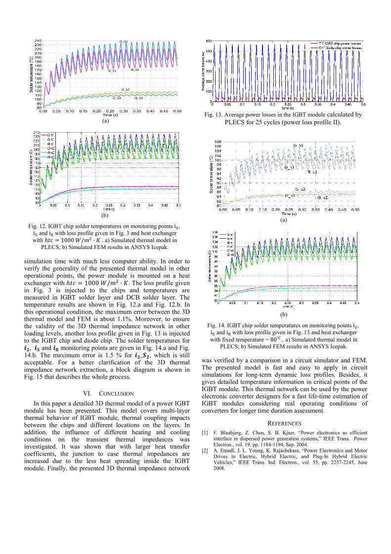
simulation time with much less computer ability. In order to verify the generality of the presented thermal model in other operational points, the power module is mounted on a heat exchanger with 1000 / · . The loss profile given in Fig. 3 is injected to the chips and temperatures are measured in IGBT solder layer and DCB solder layer. The temperature results are shown in Fig. 12.a and Fig. 12.b. In this operational condition, the maximum error between the 3D thermal model and FEM is about 1.1%. Moreover, to ensure the validity of the 3D thermal impedance network in other loading levels, another loss profile given in Fig. 13 is injected to the IGBT chip and diode chip. The solder temperatures for
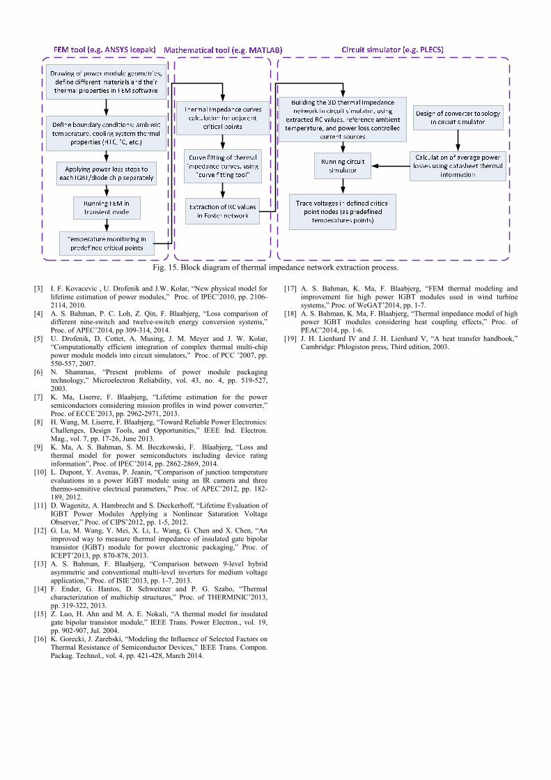
, and monitoring points are given in Fig. 14.a and Fig. 14.b. The maximum error is 1.5 % for _ , which is still acceptable. For a better clarification of the 3D thermal impedance network extraction, a block diagram is shown in Fig. 15 that describes the whole process.
VI. CONCLUSION In this paper a detailed 3D thermal model of a power IGBT
module has been presented. This model covers multi-layer thermal behavior of IGBT module, thermal coupling impacts between the chips and different locations on the layers. In addition, the influence of different heating and cooling conditions on the transient thermal impedances was investigated. It was shown that with larger heat transfer coefficients, the junction to case thermal impedances are increased due to the less heat spreading inside the IGBT module. Finally, the presented 3D thermal impedance network
was verified by a comparison in a circuit simulator and FEM. The presented model is fast and easy to apply in circuit simulations for long-term dynamic loss profiles. Besides, it gives detailed temperature information in critical points of the IGBT module. This thermal network can be used by the power electronic converter designers for a fast life-time estimation of IGBT modules considering real operating conditions of converters for longer time duration assessment.
REFERENCES [1] F. Blaabjerg, Z. Chen, S. B. Kjaer, “Power electronics as efficient
interface in dispersed power generation systems,” IEEE Trans. Power Electron., vol. 19, pp. 1184-1194, Sep. 2004.
[2] A. Emadi, J. L. Young, K. Rajashekara, “Power Electronics and Motor Drives in Electric, Hybrid Electric, and Plug-In Hybrid Electric Vehicles,” IEEE Trans. Ind. Electron., vol. 55, pp. 2237-2245, June 2008.
(a)
(b)
Fig. 12. IGBT chip solder temperatures on monitoring points i , i and i with loss profile given in Fig. 3 and heat exchanger with 1000 / · . a) Simulated thermal model in
PLECS; b) Simulated FEM results in ANSYS Icepak.
(a)
(b)
Fig. 14. IGBT chip solder temperatures on monitoring points i , i and i with loss profile given in Fig. 13 and heat exchanger with fixed temperature = 80 .. a) Simulated thermal model in
PLECS; b) Simulated FEM results in ANSYS Icepak.
Fig. 13. Average power losses in the IGBT module calculated by PLECS for 25 cycles (power loss profile II).
i5_S1
i2_S1 i8_S1
i5_S2
i2_S2 i8_S2
[3] I. F. Kovacevic , U. Drofenik and J.W. Kolar, “New physical model for lifetime estimation of power modules,” Proc. of IPEC’2010, pp. 2106-2114, 2010.
[4] A. S. Bahman, P. C. Loh, Z. Qin, F. Blaabjerg, “Loss comparison of different nine-switch and twelve-switch energy conversion systems,” Proc. of APEC’2014, pp 309-314, 2014.
[5] U. Drofenik, D. Cottet, A. Musing, J. M. Meyer and J. W. Kolar, “Computationally efficient integration of complex thermal multi-chip power module models into circuit simulators,” Proc. of PCC ’2007, pp. 550-557, 2007.
[6] N. Shammas, “Present problems of power module packaging technology,” Microelectron Reliability, vol. 43, no. 4, pp. 519-527, 2003.
[7] K. Ma, Liserre, F. Blaabjerg, “Lifetime estimation for the power semiconductors considering mission profiles in wind power converter,” Proc. of ECCE’2013, pp. 2962-2971, 2013.
[8] H. Wang, M. Liserre, F. Blaabjerg, “Toward Reliable Power Electronics: Challenges, Design Tools, and Opportunities,” IEEE Ind. Electron. Mag., vol. 7, pp. 17-26, June 2013.
[9] K. Ma, A. S. Bahman, S. M. Beczkowski, F. Blaabjerg, “Loss and thermal model for power semiconductors including device rating information”, Proc. of IPEC’2014, pp. 2862-2869, 2014.
[10] L. Dupont, Y. Avenas, P. Jeanin, “Comparison of junction temperature evaluations in a power IGBT module using an IR camera and three thermo-sensitive electrical parameters,” Proc. of APEC’2012, pp. 182-189, 2012.
[11] D. Wagenitz, A. Hambrecht and S. Dieckerhoff, “Lifetime Evaluation of IGBT Power Modules Applying a Nonlinear Saturation Voltage Observer,” Proc. of CIPS’2012, pp. 1-5, 2012.
[12] G. Lu, M. Wang, Y. Mei, X. Li, L. Wang, G. Chen and X. Chen, “An improved way to measure thermal impedance of insulated gate bipolar transistor (IGBT) module for power electronic packaging,” Proc. of ICEPT’2013, pp. 870-878, 2013.
[13] A. S. Bahman, F. Blaabjerg, “Comparison between 9-level hybrid asymmetric and conventional multi-level inverters for medium voltage application,” Proc. of ISIE’2013, pp. 1-7, 2013.
[14] F. Ender, G. Hantos, D. Schweitzer and P. G. Szabo, “Thermal characterization of multichip structures,” Proc. of THERMINIC’2013, pp. 319-322, 2013.
[15] Z. Luo, H. Ahn and M. A. E. Nokali, “A thermal model for insulated gate bipolar transistor module,” IEEE Trans. Power Electron., vol. 19, pp. 902-907, Jul. 2004.
[16] K. Gorecki, J. Zarebski, “Modeling the Influence of Selected Factors on Thermal Resistance of Semiconductor Devices,” IEEE Trans. Compon. Packag. Technol., vol. 4, pp. 421-428, March 2014.
[17] A. S. Bahman, K. Ma, F. Blaabjerg, “FEM thermal modeling and improvement for high power IGBT modules used in wind turbine systems,” Proc. of WeGAT’2014, pp. 1-7.
[18] A. S. Bahman, K. Ma, F. Blaabjerg, “Thermal impedance model of high power IGBT modules considering heat coupling effects,” Proc. of PEAC’2014, pp. 1-6.
[19] J. H. Lienhard IV and J. H. Lienhard V, “A heat transfer handbook,” Cambridge: Phlogiston press, Third edition, 2003.
Fig. 15. Block diagram of thermal impedance network extraction process.