Embed Size (px)
Citation preview
IEEE JOURNAL OF SOLID-STATE CIRCUITS, VOL. 43, NO. 2, FEBRUARY 2008 425
A Wide-Tracking Range Clock and DataRecovery Circuit
Pavan Kumar Hanumolu, Member, IEEE, Gu-Yeon Wei, Member, IEEE, and Un-Ku Moon, Senior Member, IEEE
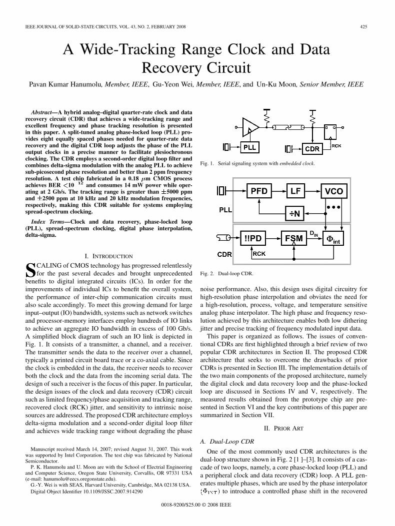
Abstract—A hybrid analog–digital quarter-rate clock and datarecovery circuit (CDR) that achieves a wide-tracking range andexcellent frequency and phase tracking resolution is presentedin this paper. A split-tuned analog phase-locked loop (PLL) pro-vides eight equally spaced phases needed for quarter-rate datarecovery and the digital CDR loop adjusts the phase of the PLLoutput clocks in a precise manner to facilitate plesiochronousclocking. The CDR employs a second-order digital loop filter andcombines delta-sigma modulation with the analog PLL to achievesub-picosecond phase resolution and better than 2 ppm frequencyresolution. A test chip fabricated in a 0.18 m CMOS processachieves BER 10 and consumes 14 mW power while oper-ating at 2 Gb/s. The tracking range is greater than 5000 ppmand 2500 ppm at 10 kHz and 20 kHz modulation frequencies,respectively, making this CDR suitable for systems employingspread-spectrum clocking.
Index Terms—Clock and data recovery, phase-locked loop(PLL), spread-spectrum clocking, digital phase interpolation,delta-sigma.
I. INTRODUCTION
SCALING of CMOS technology has progressed relentlesslyfor the past several decades and brought unprecedented
benefits to digital integrated circuits (ICs). In order for theimprovements of individual ICs to benefit the overall system,the performance of inter-chip communication circuits mustalso scale accordingly. To meet this growing demand for largeinput–output (IO) bandwidth, systems such as network switchesand processor-memory interfaces employ hundreds of IO linksto achieve an aggregate IO bandwidth in excess of 100 Gb/s.A simplified block diagram of such an IO link is depicted inFig. 1. It consists of a transmitter, a channel, and a receiver.The transmitter sends the data to the receiver over a channel,typically a printed circuit board trace or a co-axial cable. Sincethe clock is embedded in the data, the receiver needs to recoverboth the clock and the data from the incoming serial data. Thedesign of such a receiver is the focus of this paper. In particular,the design issues of the clock and data recovery (CDR) circuitsuch as limited frequency/phase acquisition and tracking range,recovered clock (RCK) jitter, and sensitivity to intrinsic noisesources are addressed. The proposed CDR architecture employsdelta-sigma modulation and a second-order digital loop filterand achieves wide tracking range without degrading the phase
Manuscript received March 14, 2007; revised August 31, 2007. This workwas supported by Intel Corporation. The test chip was fabricated by NationalSemiconductor.
P. K. Hanumolu and U. Moon are with the School of Electrial Engineeringand Computer Science, Oregon State University, Corvallis, OR 97331 USA(e-mail: [email protected]).
G.-Y. Wei is with SEAS, Harvard University, Cambridge, MA 02138 USA.Digital Object Identifier 10.1109/JSSC.2007.914290
Fig. 1. Serial signaling system with embedded clock.
Fig. 2. Dual-loop CDR.
noise performance. Also, this design uses digital circuitry forhigh-resolution phase interpolation and obviates the need fora high-resolution, process, voltage, and temperature sensitiveanalog phase interpolator. The high phase and frequency reso-lution achieved by this architecture enables both low ditheringjitter and precise tracking of frequency modulated input data.
This paper is organized as follows. The issues of conven-tional CDRs are first highlighted through a brief review of twopopular CDR architectures in Section II. The proposed CDRarchitecture that seeks to overcome the drawbacks of priorCDRs is presented in Section III. The implementation details ofthe two main components of the proposed architecture, namelythe digital clock and data recovery loop and the phase-lockedloop are discussed in Sections IV and V, respectively. Themeasured results obtained from the prototype chip are pre-sented in Section VI and the key contributions of this paper aresummarized in Section VII.
II. PRIOR ART
A. Dual-Loop CDR
One of the most commonly used CDR architectures is thedual-loop structure shown in Fig. 2 [1 ]–[3]. It consists of a cas-cade of two loops, namely, a core phase-locked loop (PLL) anda peripheral clock and data recovery (CDR) loop. A PLL gen-erates multiple phases, which are used by the phase interpolator
to introduce a controlled phase shift in the recovered
0018-9200/$25.00 © 2008 IEEE
426 IEEE JOURNAL OF SOLID-STATE CIRCUITS, VOL. 43, NO. 2, FEBRUARY 2008
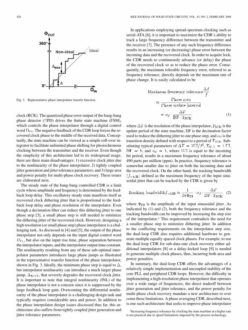
Fig. 3. Representative phase interpolator transfer function.
clock (RCK). The quantized phase error output of the bang-bangphase detector (!!PD) drives the finite state machine (FSM),which controls the phase interpolator through a digital controlword . The negative feedback of the CDR loop forces the re-covered clock phase to the middle of the received data. Concep-tually, the state machine can be viewed as a simple roll-over in-tegrator to facilitate unlimited phase shifting for plesiochronousclocking between the transmitter and the receiver. Even thoughthe simplicity of this architecture led to its widespread usage,there are three main disadvantages: 1) excessive clock jitter dueto the nonlinearity of the phase interpolator; 2) tightly coupledjitter generation and jitter tolerance parameters; and 3) large areaand power penalty for multi-phase clock recovery. These issuesare elaborated next.
The steady state of the bang-bang controlled CDR is a limitcycle whose amplitude and frequency is determined by the feed-back loop delay. This oscillatory steady state manifests itself asrecovered clock dithering jitter that is proportional to the feed-back loop delay and phase resolution of the interpolator. Eventhough a decimation filter can reduce this dithering jitter to onephase step [3], a small phase step is still needed to minimizethe dithering jitter of the recovered clock. However, designing ahigh resolution (or small phase step) phase interpolator is a chal-lenging task. As discussed in [4] and [5], the output of the phaseinterpolator not only depends on the input digital control word
, but also on the input rise time, phase separation betweenthe interpolator inputs, and the interpolator output time constant.The nonlinearity resulting from any of these sub-optimal inter-polator parameters introduces large phase jumps as illustratedin the representative transfer function of the phase interpolator,shown in Fig. 3. Ideally, the minimum phase step is equal to ,but interpolator nonlinearity can introduce a much larger phasejump, , that severely degrades the recovered clock jitter.It is important to note that integral nonlinearity (INL) of thephase interpolator is not a concern since it is suppressed by thelarge feedback loop gain. Overcoming the differential nonlin-earity of the phase interpolator is a challenging design task andtypically requires considerable area and power. In addition tothe phase interpolator design issues discussed thus far, this ar-chitecture also suffers from tightly coupled jitter generation andjitter tolerance parameters.
In applications employing spread-spectrum clocking such asserial-ATA [6], it is important to maximize the CDR’s ability totrack a large frequency difference between the transmitter andthe receiver [7]. The presence of any such frequency differenceresults in an increasing (or decreasing) phase error between theincoming data and the recovered clock. In order to acquire lock,the CDR needs to continuously advance (or delay) the phaseof the recovered clock so as to reduce the phase error. Conse-quently, the maximum tolerable frequency error, referred to asfrequency tolerance, directly depends on the maximum rate ofphase change. It is easily calculated to be
(1)
where is the resolution of the phase interpolator, is theupdate period of the state machine, DF is the decimation factorused to reduce the dithering jitter to one phase step, and is thetransition density defined with respect to a period of . Sub-stituting typical parameters of , ,
, and , where is equal to the incomingbit period, results in a maximum frequency tolerance of about490 parts per million (ppm). In practice, frequency tolerance issomewhat smaller due to jitter on both the incoming data andthe recovered clock. On the other hand, the tracking bandwidth
defined as the maximum frequency of the input sinu-soidal jitter that can be tracked by the CDR is given by
(2)
where is the amplitude of the input sinusoidal jitter. Asindicated by (1) and (2), both the frequency tolerance and thetracking bandwidth can be improved by increasing the step sizeof the interpolator.1 This requirement contradicts the need fora smaller phase step to minimize dithering jitter. In additionto the conflicting requirements on the interpolator step size,the dual-loop CDR also requires additional hardware to gen-erate multiple equally spaced clock phases. For example, to usethe dual-loop CDR for sub-data-rate clock recovery either ad-ditional interpolators [8] or a delay-locked loop [9] is neededto generate multiple clock phases, thus, incurring both area andpower penalties.
In summary, the dual-loop CDR offers the advantages of arelatively simple implementation and uncoupled stability of thecore PLL and peripheral CDR loops. However, the difficulty inimplementing a high-resolution phase interpolator that operatesover a wide range of frequencies, the direct tradeoff betweenjitter generation and jitter tolerance, and the power penalty formulti-phase clock recovery mandate a new architecture to overcome these limitations. A phase averaging CDR, described next,is one such architecture that seeks to improve phase interpolator
1Increasing frequency tolerance by clocking the state machine at a higher rateis not practical due to speed limitations imposed by the process technology.
HANUMOLU et al.: A WIDE-TRACKING RANGE CLOCK AND DATA RECOVERY CIRCUIT 427
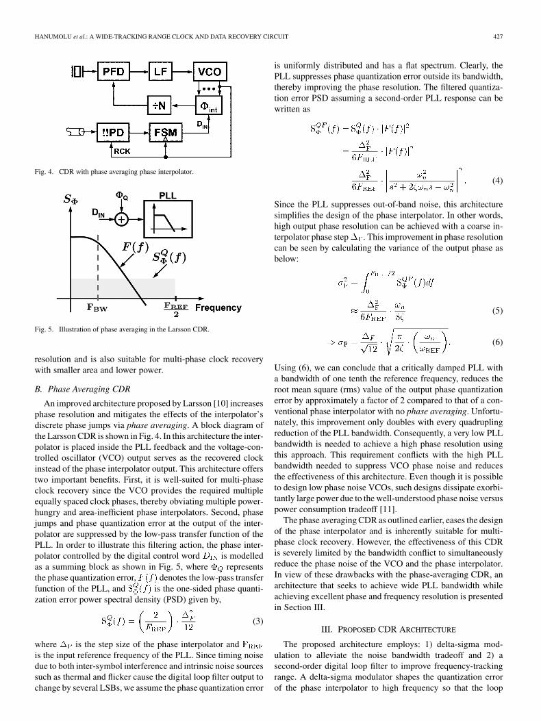
Fig. 4. CDR with phase averaging phase interpolator.
Fig. 5. Illustration of phase averaging in the Larsson CDR.
resolution and is also suitable for multi-phase clock recoverywith smaller area and lower power.
B. Phase Averaging CDR
An improved architecture proposed by Larsson [10] increasesphase resolution and mitigates the effects of the interpolator’sdiscrete phase jumps via phase averaging. A block diagram ofthe Larsson CDR is shown in Fig. 4. In this architecture the inter-polator is placed inside the PLL feedback and the voltage-con-trolled oscillator (VCO) output serves as the recovered clockinstead of the phase interpolator output. This architecture offerstwo important benefits. First, it is well-suited for multi-phaseclock recovery since the VCO provides the required multipleequally spaced clock phases, thereby obviating multiple power-hungry and area-inefficient phase interpolators. Second, phasejumps and phase quantization error at the output of the inter-polator are suppressed by the low-pass transfer function of thePLL. In order to illustrate this filtering action, the phase inter-polator controlled by the digital control word is modelledas a summing block as shown in Fig. 5, where representsthe phase quantization error, denotes the low-pass transferfunction of the PLL, and is the one-sided phase quanti-zation error power spectral density (PSD) given by,
(3)
where is the step size of the phase interpolator andis the input reference frequency of the PLL. Since timing noisedue to both inter-symbol interference and intrinsic noise sourcessuch as thermal and flicker cause the digital loop filter output tochange by several LSBs, we assume the phase quantization error
is uniformly distributed and has a flat spectrum. Clearly, thePLL suppresses phase quantization error outside its bandwidth,thereby improving the phase resolution. The filtered quantiza-tion error PSD assuming a second-order PLL response can bewritten as
(4)
Since the PLL suppresses out-of-band noise, this architecturesimplifies the design of the phase interpolator. In other words,high output phase resolution can be achieved with a coarse in-terpolator phase step . This improvement in phase resolutioncan be seen by calculating the variance of the output phase asbelow:
(5)
(6)
Using (6), we can conclude that a critically damped PLL witha bandwidth of one tenth the reference frequency, reduces theroot mean square (rms) value of the output phase quantizationerror by approximately a factor of 2 compared to that of a con-ventional phase interpolator with no phase averaging. Unfortu-nately, this improvement only doubles with every quadruplingreduction of the PLL bandwidth. Consequently, a very low PLLbandwidth is needed to achieve a high phase resolution usingthis approach. This requirement conflicts with the high PLLbandwidth needed to suppress VCO phase noise and reducesthe effectiveness of this architecture. Even though it is possibleto design low phase noise VCOs, such designs dissipate exorbi-tantly large power due to the well-understood phase noise versuspower consumption tradeoff [11].
The phase averaging CDR as outlined earlier, eases the designof the phase interpolator and is inherently suitable for multi-phase clock recovery. However, the effectiveness of this CDRis severely limited by the bandwidth conflict to simultaneouslyreduce the phase noise of the VCO and the phase interpolator.In view of these drawbacks with the phase-averaging CDR, anarchitecture that seeks to achieve wide PLL bandwidth whileachieving excellent phase and frequency resolution is presentedin Section III.
III. PROPOSED CDR ARCHITECTURE
The proposed architecture employs: 1) delta-sigma mod-ulation to alleviate the noise bandwidth tradeoff and 2) asecond-order digital loop filter to improve frequency-trackingrange. A delta-sigma modulator shapes the quantization errorof the phase interpolator to high frequency so that the loop
428 IEEE JOURNAL OF SOLID-STATE CIRCUITS, VOL. 43, NO. 2, FEBRUARY 2008
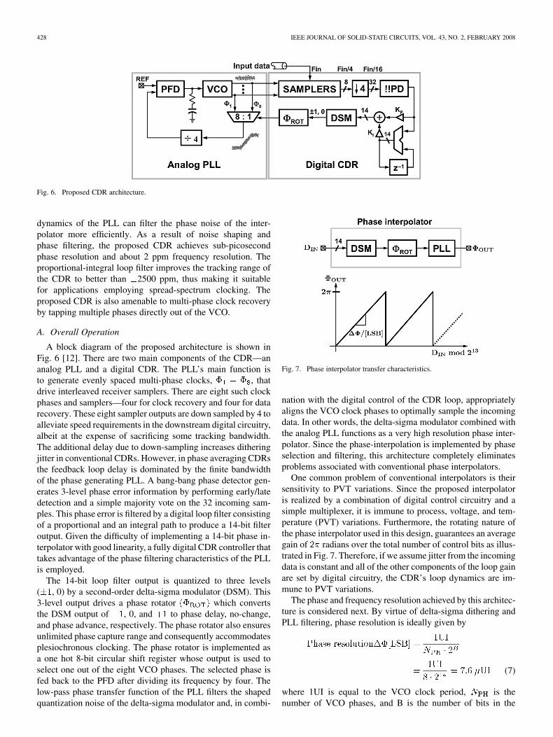
Fig. 6. Proposed CDR architecture.
dynamics of the PLL can filter the phase noise of the inter-polator more efficiently. As a result of noise shaping andphase filtering, the proposed CDR achieves sub-picosecondphase resolution and about 2 ppm frequency resolution. Theproportional-integral loop filter improves the tracking range ofthe CDR to better than 2500 ppm, thus making it suitablefor applications employing spread-spectrum clocking. Theproposed CDR is also amenable to multi-phase clock recoveryby tapping multiple phases directly out of the VCO.
A. Overall Operation
A block diagram of the proposed architecture is shown inFig. 6 [12]. There are two main components of the CDR—ananalog PLL and a digital CDR. The PLL’s main function isto generate evenly spaced multi-phase clocks, , thatdrive interleaved receiver samplers. There are eight such clockphases and samplers—four for clock recovery and four for datarecovery. These eight sampler outputs are down sampled by 4 toalleviate speed requirements in the downstream digital circuitry,albeit at the expense of sacrificing some tracking bandwidth.The additional delay due to down-sampling increases ditheringjitter in conventional CDRs. However, in phase averaging CDRsthe feedback loop delay is dominated by the finite bandwidthof the phase generating PLL. A bang-bang phase detector gen-erates 3-level phase error information by performing early/latedetection and a simple majority vote on the 32 incoming sam-ples. This phase error is filtered by a digital loop filter consistingof a proportional and an integral path to produce a 14-bit filteroutput. Given the difficulty of implementing a 14-bit phase in-terpolator with good linearity, a fully digital CDR controller thattakes advantage of the phase filtering characteristics of the PLLis employed.
The 14-bit loop filter output is quantized to three levels( , 0) by a second-order delta-sigma modulator (DSM). This3-level output drives a phase rotator which convertsthe DSM output of , 0, and to phase delay, no-change,and phase advance, respectively. The phase rotator also ensuresunlimited phase capture range and consequently accommodatesplesiochronous clocking. The phase rotator is implemented asa one hot 8-bit circular shift register whose output is used toselect one out of the eight VCO phases. The selected phase isfed back to the PFD after dividing its frequency by four. Thelow-pass phase transfer function of the PLL filters the shapedquantization noise of the delta-sigma modulator and, in combi-
Fig. 7. Phase interpolator transfer characteristics.
nation with the digital control of the CDR loop, appropriatelyaligns the VCO clock phases to optimally sample the incomingdata. In other words, the delta-sigma modulator combined withthe analog PLL functions as a very high resolution phase inter-polator. Since the phase-interpolation is implemented by phaseselection and filtering, this architecture completely eliminatesproblems associated with conventional phase interpolators.
One common problem of conventional interpolators is theirsensitivity to PVT variations. Since the proposed interpolatoris realized by a combination of digital control circuitry and asimple multiplexer, it is immune to process, voltage, and tem-perature (PVT) variations. Furthermore, the rotating nature ofthe phase interpolator used in this design, guarantees an averagegain of radians over the total number of control bits as illus-trated in Fig. 7. Therefore, if we assume jitter from the incomingdata is constant and all of the other components of the loop gainare set by digital circuitry, the CDR’s loop dynamics are im-mune to PVT variations.
The phase and frequency resolution achieved by this architec-ture is considered next. By virtue of delta-sigma dithering andPLL filtering, phase resolution is ideally given by
(7)
where 1UI is equal to the VCO clock period, is thenumber of VCO phases, and B is the number of bits in the
HANUMOLU et al.: A WIDE-TRACKING RANGE CLOCK AND DATA RECOVERY CIRCUIT 429
loop filter output. Quantitatively, there are phases in be-tween the adjacent phases of the VCO. In practice, however,incomplete filtering of the shaped noise lowers the resolutionfrom this ideal value and frequency resolution is determinedby the rate at which the VCO phase can be updated by theCDR loop. Assuming integral gain to be , the CDR loopcan increment/decrement the VCO phase by phase stepsevery update period, . In the proposed architecture,the update rate is 4 times slower than the VCO clock frequency.Consequently, the frequency resolution can be expressed as
(8)
ppm (9)
Using parameters from the prototype, better than 2 ppm fre-quency resolution is achieved. Note that it is also possible toachieve higher phase/frequency resolution by simply choosinga larger number of loop filter bits at the expense of proportionalreduction in tracking bandwidth.
B. Phase and Frequency Tracking
The tracking bandwidth of this CDR depends on both theinput jitter amplitude and frequency as shown earlier by (2).This equation derived for a dual-loop CDR is also valid for theproposed architecture. It indicates that if the input jitter has largeamplitude or if it varies with high frequency, the CDR slews,and as a result the output phase cannot track the input jitter. Inthis architecture, the integral path in the loop filter extends thetracking bandwidth of the CDR. In the presence of a large phaseerror, the bang-bang phase detector is overloaded and outputsa long string of ’s or ’s. The integrator accumulates thiscontinuous stream of identical outputs and drives the VCO to-ward frequency lock. In the prototype, with an integral gainequal to one, the integral loop moves the VCO center frequencyin steps of about 2 ppm. The tracking range of the CDR, definedas the range of input frequencies the CDR can track withoutlosing lock, is equal to
ppm (10)
is the width of the integrator output and is the fre-quency resolution. An extra factor of one half in this equation isused to accommodate the fact that only about half the full-scalerange of the delta-sigma modulator is used in this design.2 Usinga 14-bit integrator and a frequency resolution of 2 ppm, theCDR has 7780 ppm of frequency tracking range. This ratherlarge tracking range is valid only if the input data frequencyvaries at a slow rate. If the frequency varies at a rate faster than
2The full-scale input to the 3-level DSM overloads the internal quantizerand degrades noise shaping significantly and may even cause instability. It isa common practice to limit the DSM input through scaling or by some othermeans [13].
Fig. 8. Block diagram of the CDR used for stability analysis.
, the integral loop will not be able to move theVCO frequency fast enough to track it. As a result, the integralloop slews and the phase error grows quadratically, causing theCDR to eventually lose lock.
C. Lock Range
We have thus far discussed the tracking properties of the pro-posed CDR. However, this analysis is based on the assumptionthat the CDR is in phase lock. When the CDR is not phaselocked, and if the frequency difference between the incomingdata and the local VCO frequency is small, the proportional pathwill acquire phase lock without cycle slipping. In other words,if the phase error resulting from the frequency error varies ata rate slower than the phase tracking range of the proportionalpath, phase lock will be achieved. Therefore, the lock range, de-fined as the range of frequencies within which the CDR acquiresphase lock without cycle slipping is given by
ppm (11)
is the proportional gain and is equal to 128 in the prototypechip. This lock range is adequate to accommodate the ppmfrequency tolerance of commercial crystal oscillators.
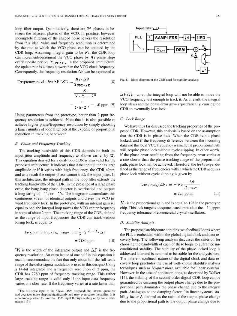
D. Stability Analysis
The proposed architecture contains two feedback loops wherethe PLL is embedded within the global digital clock and data re-covery loop. The following analysis discusses the criterion forchoosing the bandwidth of each of these loops to guarantee un-conditional stability. The stability of the phase-locked loop isaddressed later and is assumed to be stable for the analysis here.The inherent nonlinear nature of the digital clock and data re-covery loop precludes the use of well-known stability-analysistechniques such as Nyquist plots, available for linear systems.However, in the case of nonlinear loops, as described by Walker[14], the stability of the second-order digital CDR loop can beguaranteed by ensuring the output phase change due to the pro-portional path dominates the phase change due to the integralpath. Analogous to the damping factor in linear systems, sta-bility factor , defined as the ratio of the output phase changedue to the proportional path to the output phase change due to
430 IEEE JOURNAL OF SOLID-STATE CIRCUITS, VOL. 43, NO. 2, FEBRUARY 2008
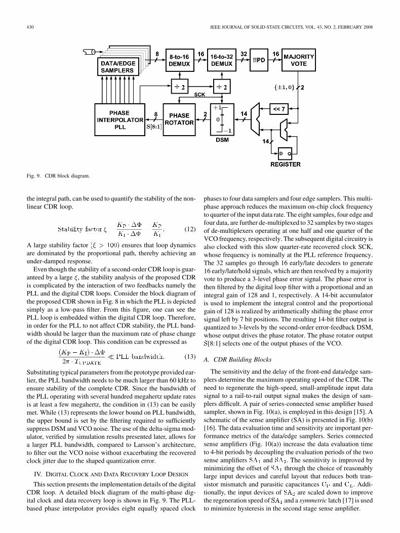
Fig. 9. CDR block diagram.
the integral path, can be used to quantify the stability of the non-linear CDR loop.
(12)
A large stability factor ensures that loop dynamicsare dominated by the proportional path, thereby achieving anunder-damped response.
Even though the stability of a second-order CDR loop is guar-anteed by a large , the stability analysis of the proposed CDRis complicated by the interaction of two feedbacks namely thePLL and the digital CDR loops. Consider the block diagram ofthe proposed CDR shown in Fig. 8 in which the PLL is depictedsimply as a low-pass filter. From this figure, one can see thePLL loop is embedded within the digital CDR loop. Therefore,in order for the PLL to not affect CDR stability, the PLL band-width should be larger than the maximum rate of phase changeof the digital CDR loop. This condition can be expressed as
(13)
Substituting typical parameters from the prototype provided ear-lier, the PLL bandwidth needs to be much larger than 60 kHz toensure stability of the complete CDR. Since the bandwidth ofthe PLL operating with several hundred megahertz update ratesis at least a few megahertz, the condition in (13) can be easilymet. While (13) represents the lower bound on PLL bandwidth,the upper bound is set by the filtering required to sufficientlysuppress DSM and VCO noise. The use of the delta-sigma mod-ulator, verified by simulation results presented later, allows fora larger PLL bandwidth, compared to Larsson’s architecture,to filter out the VCO noise without exacerbating the recoveredclock jitter due to the shaped quantization error.
IV. DIGITAL CLOCK AND DATA RECOVERY LOOP DESIGN
This section presents the implementation details of the digitalCDR loop. A detailed block diagram of the multi-phase dig-ital clock and data recovery loop is shown in Fig. 9. The PLL-based phase interpolator provides eight equally spaced clock
phases to four data samplers and four edge samplers. This multi-phase approach reduces the maximum on-chip clock frequencyto quarter of the input data rate. The eight samples, four edge andfour data, are further de-multiplexed to 32 samples by two stagesof de-multiplexers operating at one half and one quarter of theVCO frequency, respectively. The subsequent digital circuitry isalso clocked with this slow quarter-rate recovered clock SCK,whose frequency is nominally at the PLL reference frequency.The 32 samples go through 16 early/late decoders to generate16 early/late/hold signals, which are then resolved by a majorityvote to produce a 3-level phase error signal. The phase error isthen filtered by the digital loop filter with a proportional and anintegral gain of 128 and 1, respectively. A 14-bit accumulatoris used to implement the integral control and the proportionalgain of 128 is realized by arithmetically shifting the phase errorsignal left by 7 bit positions. The resulting 14-bit filter output isquantized to 3-levels by the second-order error-feedback DSM,whose output drives the phase rotator. The phase rotator output
[8:1] selects one of the output phases of the VCO.
A. CDR Building Blocks
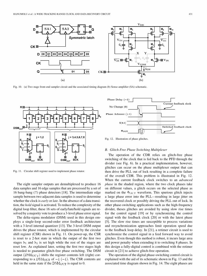
The sensitivity and the delay of the front-end data/edge sam-plers determine the maximum operating speed of the CDR. Theneed to regenerate the high-speed, small-amplitude input datasignal to a rail-to-rail output signal makes the design of sam-plers difficult. A pair of series-connected sense amplifier basedsampler, shown in Fig. 10(a), is employed in this design [15]. Aschematic of the sense amplifier (SA) is presented in Fig. 10(b)[16]. The data evaluation time and sensitivity are important per-formance metrics of the data/edge samplers. Series connectedsense amplifiers (Fig. 10(a)) increase the data evaluation timeto 4-bit periods by decoupling the evaluation periods of the twosense amplifiers and . The sensitivity is improved byminimizing the offset of through the choice of reasonablylarge input devices and careful layout that reduces both tran-sistor mismatch and parasitic capacitances and . Addi-tionally, the input devices of are scaled down to improvethe regeneration speed of and a symmetric latch [17] is usedto minimize hysteresis in the second stage sense amplifier.
HANUMOLU et al.: A WIDE-TRACKING RANGE CLOCK AND DATA RECOVERY CIRCUIT 431
Fig. 10. (a) Two stage front-end sampler circuit and the associated timing diagram (b) Sense-amplifier (SA) schematic.
Fig. 11. Circular shift register used to implement phase rotator.
The eight sampler outputs are demultiplexed to produce 16data samples and 16 edge samples that are processed by a set of16 bang-bang (!!) phase detectors [18]. The intermediate edgesample between two adjacent data samples is used to determinewhether the clock is early or late. In the absence of a data transi-tion, the hold signal is activated. To reduce the complexity of thedigital loop filter, these 16 sets of early/late/hold signals are re-solved by a majority vote to produce a 3-level phase error signal.
The delta-sigma modulator (DSM) used in this design em-ploys a single-loop second-order error feedback architecturewith a 3-level internal quantizer [13]. The 3-level DSM outputdrives the phase rotator, which is implemented by the circularshift register (CSR) shown in Fig. 11. On power-up, the CSRis reset to a 2-hot state in which the output of the first twostages and is set high while the rest of the stages arereset low. As explained later, setting the first two stages highis needed to guarantee glitch-free phase switching. The DSMoutput shifts the register contents left (right) cor-responding to a of . The CSR contents areheld in the same state if the is equal to 0.
Fig. 12. Illustration of phase glitches.
B. Glitch-Free Phase Switching Multiplexer
The operation of the CDR relies on glitch-free phaseswitching of the clock that is fed back to the PFD through thedivider (see Fig. 6). In a practical implementation, however,glitches can occur on the phase multiplexer output that canthen drive the PLL out of lock resulting in a complete failureof the overall CDR. This problem is illustrated in Fig. 12.When the current feedback clock switches to an advancedphase in the shaded region, where the two clock phases takeon different values, a glitch occurs on the selected phase asmarked on the waveform. This spurious glitch injectsa large phase error into the PLL—resulting in large jitter onthe recovered clock or possibly driving the PLL out of lock. Inother phase-switching applications such as the high-frequencydivider, theses glitches are avoided by using slow rise timesfor the control signal [19] or by synchronizing the controlsignal with the feedback clock [20] or with the latest phase[5]. The slow rise times are susceptible to process variationsand resynchronization approaches limit operation speed dueto the feedback loop delay. In [21], a retimer circuit is used tosynchronize the control signal in a feed forward way to avoidglitches. Even though this method is robust, it incurs large areaand power penalty when extending it to switching 8 phases. Inthis design a fully-digital control is combined with the retimercircuit in [21] to achieve glitch-free operation.
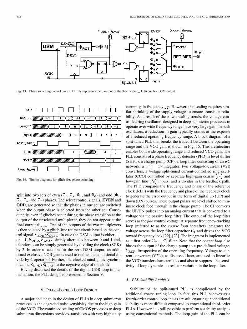
The operation of the digital phase-switching control circuit isexplained with the aid of its schematic shown in Fig. 13 and theassociated time diagram shown in Fig. 14. The eight phases are
432 IEEE JOURNAL OF SOLID-STATE CIRCUITS, VOL. 43, NO. 2, FEBRUARY 2008
Fig. 13. Phase switching control circuit. represents the 0 output of the 3-bit wide ( , 0) one hot DSM output.
Fig. 14. Timing diagrams for glitch-free phase switching.
split into two sets of even ( , , , and ) and odd ( ,, , and ) phases. The select control signals, EVEN and
ODD, are generated so that the phases in one set are switchedwhen the output phase is selected from the other set. Conse-quently, even if glitches occur during the phase transition at theoutput of the unselected multiplexer, they do not appear at thefinal output . One of the outputs of the two multiplexersis then selected by a glitch-free retimer circuit based on the con-trol signal . In case the DSM output is eitheror , simply alternates between 0 and 1 and,therefore, can be simply generated by dividing the clock (SCK)by 2. In order to account for the zero DSM output, an addi-tional exclusive NOR gate is used to realize the conditional di-vide-by-2 operation. Further, the clocked nand gates synchro-nize the to the negative edge of the clock.
Having discussed the details of the digital CDR loop imple-mentation, the PLL design is presented in Section V.
V. PHASE-LOCKED LOOP DESIGN
A major challenge in the design of PLLs in deep submicronprocesses is the degraded noise sensitivity due to the high gainof the VCO. The continued scaling of CMOS processes to deepsubmicron dimensions provides transistors with very high unity
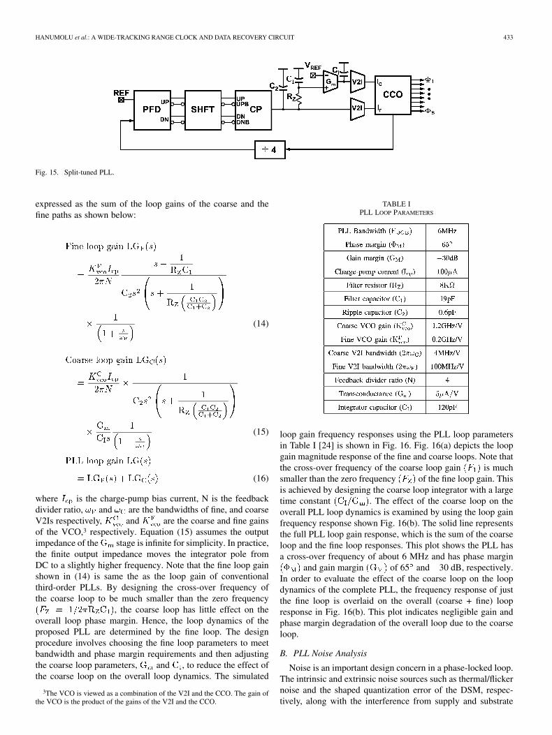
current gain frequency . However, this scaling requires sim-ilar shrinking of the supply voltage to ensure transistor relia-bility. As a result of these two scaling trends, the voltage-con-trolled ring oscillators designed in deep submicron processes tooperate over wide frequency range have very large gain. In suchoscillators, a reduction in gain typically comes at the expenseof a reduced operating frequency range. A block diagram of asplit-tuned PLL that breaks the tradeoff between the operatingrange and the VCO gain is shown in Fig. 15. This architectureenables both wide operating range and reduced VCO gain. ThePLL consists of a phase frequency detector (PFD), a level shifter(SHFT), a charge pump (CP), a loop filter consisting of an RCnetwork, a integrator, two voltage-to-current (V2I)converters, a 4-stage split-tuned current-controlled ring oscil-lator (CCO) controlled by separate high-gain coarse andlow-gain fine inputs, and a divider in the feedback path.The PFD compares the frequency and phase of the referenceclock (REF) with the frequency and phase of the feedback clockto generate the error output in the form of digital up (UP) anddown (DN) pulses. These output pulses are level shifted to min-imize clock feed through in the charge pump. The CP convertsthe UP/DN pulses into an analog current that is converted to avoltage via the passive loop filter. The output of the loop filterserves as the fine control voltage. A separate frequency-trackingloop (referred to as the coarse loop hereafter) integrates thevoltage across the loop filter capacitor and drives the VCOtoward frequency lock [22], [23]. The integrator is implementedas a first order filter. Note that the coarse loop alsobiases the output of the charge pump to a pre-defined voltage,
, irrespective of the operating frequency. Voltage-to-cur-rent converters (V2Is), as discussed later, are used to linearizethe VCO transfer characteristics and also to suppress the sensi-tivity of loop dynamics to resistor variation in the loop filter.
A. PLL Stability Analysis
Stability of the split-tuned PLL is complicated by theadditional coarse tuning loop. In fact, this PLL behaves as afourth-order control loop and as a result, ensuring unconditionalstability is more difficult compared to conventional third-orderPLLs. However, it is still possible to perform a stability analysisusing conventional methods. The loop gain of the PLL can be
HANUMOLU et al.: A WIDE-TRACKING RANGE CLOCK AND DATA RECOVERY CIRCUIT 433
Fig. 15. Split-tuned PLL.
expressed as the sum of the loop gains of the coarse and thefine paths as shown below:
(14)
(15)
(16)
where is the charge-pump bias current, N is the feedbackdivider ratio, and are the bandwidths of fine, and coarseV2Is respectively, and are the coarse and fine gainsof the VCO,3 respectively. Equation (15) assumes the outputimpedance of the stage is infinite for simplicity. In practice,the finite output impedance moves the integrator pole fromDC to a slightly higher frequency. Note that the fine loop gainshown in (14) is same the as the loop gain of conventionalthird-order PLLs. By designing the cross-over frequency ofthe coarse loop to be much smaller than the zero frequency
, the coarse loop has little effect on theoverall loop phase margin. Hence, the loop dynamics of theproposed PLL are determined by the fine loop. The designprocedure involves choosing the fine loop parameters to meetbandwidth and phase margin requirements and then adjustingthe coarse loop parameters, and , to reduce the effect ofthe coarse loop on the overall loop dynamics. The simulated
3The VCO is viewed as a combination of the V2I and the CCO. The gain ofthe VCO is the product of the gains of the V2I and the CCO.
TABLE IPLL LOOP PARAMETERS
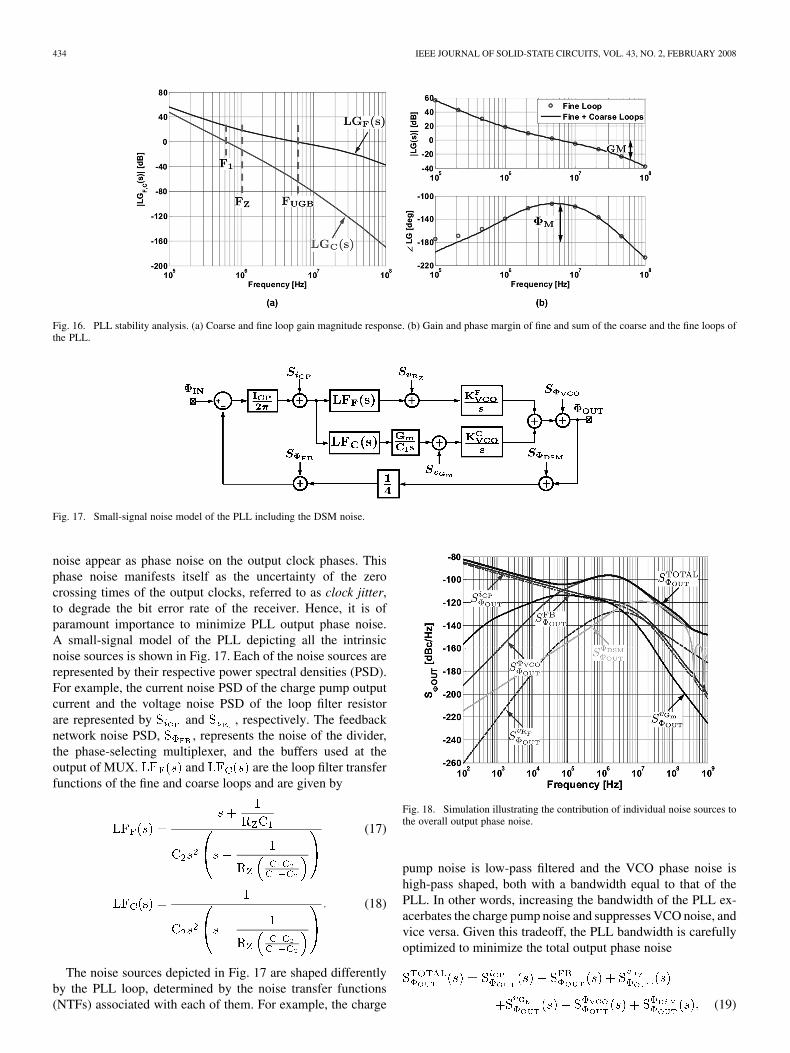
loop gain frequency responses using the PLL loop parametersin Table I [24] is shown in Fig. 16. Fig. 16(a) depicts the loopgain magnitude response of the fine and coarse loops. Note thatthe cross-over frequency of the coarse loop gain is muchsmaller than the zero frequency of the fine loop gain. Thisis achieved by designing the coarse loop integrator with a largetime constant . The effect of the coarse loop on theoverall PLL loop dynamics is examined by using the loop gainfrequency response shown Fig. 16(b). The solid line representsthe full PLL loop gain response, which is the sum of the coarseloop and the fine loop responses. This plot shows the PLL hasa cross-over frequency of about 6 MHz and has phase margin
and gain margin of 65 and 30 dB, respectively.In order to evaluate the effect of the coarse loop on the loopdynamics of the complete PLL, the frequency response of justthe fine loop is overlaid on the overall (coarse + fine) loopresponse in Fig. 16(b). This plot indicates negligible gain andphase margin degradation of the overall loop due to the coarseloop.
B. PLL Noise Analysis
Noise is an important design concern in a phase-locked loop.The intrinsic and extrinsic noise sources such as thermal/flickernoise and the shaped quantization error of the DSM, respec-tively, along with the interference from supply and substrate
434 IEEE JOURNAL OF SOLID-STATE CIRCUITS, VOL. 43, NO. 2, FEBRUARY 2008
Fig. 16. PLL stability analysis. (a) Coarse and fine loop gain magnitude response. (b) Gain and phase margin of fine and sum of the coarse and the fine loops ofthe PLL.
Fig. 17. Small-signal noise model of the PLL including the DSM noise.
noise appear as phase noise on the output clock phases. Thisphase noise manifests itself as the uncertainty of the zerocrossing times of the output clocks, referred to as clock jitter,to degrade the bit error rate of the receiver. Hence, it is ofparamount importance to minimize PLL output phase noise.A small-signal model of the PLL depicting all the intrinsicnoise sources is shown in Fig. 17. Each of the noise sources arerepresented by their respective power spectral densities (PSD).For example, the current noise PSD of the charge pump outputcurrent and the voltage noise PSD of the loop filter resistorare represented by and , respectively. The feedbacknetwork noise PSD, , represents the noise of the divider,the phase-selecting multiplexer, and the buffers used at theoutput of MUX. and are the loop filter transferfunctions of the fine and coarse loops and are given by
(17)
(18)
The noise sources depicted in Fig. 17 are shaped differentlyby the PLL loop, determined by the noise transfer functions(NTFs) associated with each of them. For example, the charge
Fig. 18. Simulation illustrating the contribution of individual noise sources tothe overall output phase noise.
pump noise is low-pass filtered and the VCO phase noise ishigh-pass shaped, both with a bandwidth equal to that of thePLL. In other words, increasing the bandwidth of the PLL ex-acerbates the charge pump noise and suppresses VCO noise, andvice versa. Given this tradeoff, the PLL bandwidth is carefullyoptimized to minimize the total output phase noise
(19)
HANUMOLU et al.: A WIDE-TRACKING RANGE CLOCK AND DATA RECOVERY CIRCUIT 435
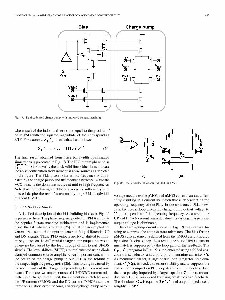
Fig. 19. Replica-biased charge pump with improved current matching.
where each of the individual terms are equal to the product ofnoise PSD with the squared magnitude of the correspondingNTF. For example, is calculated as follows:
(20)
The final result obtained from noise bandwidth optimizationsimulations is presented in Fig. 18. The PLL output phase noise
is shown by the thick solid line. Other lines indicatethe noise contribution from individual noise sources as depictedin the figure. The PLL phase noise at low frequency is domi-nated by the charge pump and the feedback network, while theVCO noise is the dominant source at mid-to-high frequencies.Note that the delta-sigma dithering noise is sufficiently sup-pressed despite the use of a reasonably large PLL bandwidthof about 6 MHz.
C. PLL Building Blocks
A detailed description of the PLL building blocks in Fig. 15is presented here. The phase frequency detector (PFD) employsthe popular 3-state machine architecture and is implementedusing the latch-based structure [25]. Small cross-coupled in-verters are used at the output to generate fully differential UPand DN signals. These PFD outputs are level shifted to mini-mize glitches on the differential charge pump output that wouldotherwise be caused by the feed-through of rail-to-rail UP/DNsignals. The level shifters (SHFT) are implemented using diodeclamped common source amplifiers. An important concern inthe design of the charge pump in our PLL is the folding ofthe shaped high-frequency noise [26]. This folding is caused bythe nonlinearity of the charge pump resulting from current mis-match. There are two major sources of UP/DOWN current mis-match in a charge pump. First, the inherent mismatch betweenthe UP current (PMOS) and the DN current (NMOS) sourcesintroduces a static error. Second, a varying charge pump output
Fig. 20. V2I circuits. (a) Coarse V2I. (b) Fine V2I.
voltage modulates the pMOS and nMOS current sources differ-ently resulting in a current mismatch that is dependent on theoperating frequency of the PLL. In the split-tuned PLL, how-ever, the coarse loop drives the charge-pump output voltage to
independent of the operating frequency. As a result, theUP and DOWN current mismatch due to a varying charge pumpoutput voltage is eliminated.
The charge-pump circuit shown in Fig. 19 uses replica bi-asing to suppress the static current mismatch. The bias for thepMOS current source is derived from the nMOS current sourceby a slow feedback loop. As a result, the static UP/DN currentmismatch is suppressed by the loop gain of the feedback. The
integrator in Fig. 15 is implemented using a folded-cas-code transconductor and a poly-poly integrating capacitor .As mentioned earlier, a large coarse loop integrator time con-stant, , is needed to ensure stability and to suppress thecoarse loop’s impact on PLL loop dynamics. In order to reducethe area penalty imposed by a large capacitor , the transcon-ductance is minimized by using weak positive feedback.The simulated is equal to 5 and output impedance isroughly 72 M .
436 IEEE JOURNAL OF SOLID-STATE CIRCUITS, VOL. 43, NO. 2, FEBRUARY 2008
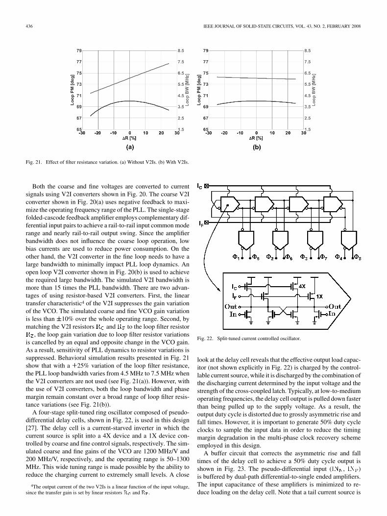
Fig. 21. Effect of filter resistance variation. (a) Without V2Is. (b) With V2Is.
Both the coarse and fine voltages are converted to currentsignals using V2I converters shown in Fig. 20. The coarse V2Iconverter shown in Fig. 20(a) uses negative feedback to maxi-mize the operating frequency range of the PLL. The single-stagefolded-cascode feedback amplifier employs complementary dif-ferential input pairs to achieve a rail-to-rail input common moderange and nearly rail-to-rail output swing. Since the amplifierbandwidth does not influence the coarse loop operation, lowbias currents are used to reduce power consumption. On theother hand, the V2I converter in the fine loop needs to have alarge bandwidth to minimally impact PLL loop dynamics. Anopen loop V2I converter shown in Fig. 20(b) is used to achievethe required large bandwidth. The simulated V2I bandwidth ismore than 15 times the PLL bandwidth. There are two advan-tages of using resistor-based V2I converters. First, the lineartransfer characteristic4 of the V2I suppresses the gain variationof the VCO. The simulated coarse and fine VCO gain variationis less than 10% over the whole operating range. Second, bymatching the V2I resistors and to the loop filter resistor
, the loop gain variation due to loop filter resistor variationsis cancelled by an equal and opposite change in the VCO gain.As a result, sensitivity of PLL dynamics to resistor variations issuppressed. Behavioral simulation results presented in Fig. 21show that with a 25% variation of the loop filter resistance,the PLL loop bandwidth varies from 4.5 MHz to 7.5 MHz whenthe V2I converters are not used (see Fig. 21(a)). However, withthe use of V2I converters, both the loop bandwidth and phasemargin remain constant over a broad range of loop filter resis-tance variations (see Fig. 21(b)).
A four-stage split-tuned ring oscillator composed of pseudo-differential delay cells, shown in Fig. 22, is used in this design[27]. The delay cell is a current-starved inverter in which thecurrent source is split into a 4X device and a 1X device con-trolled by coarse and fine control signals, respectively. The sim-ulated coarse and fine gains of the VCO are 1200 MHz/V and200 MHz/V, respectively, and the operating range is 50–1300MHz. This wide tuning range is made possible by the ability toreduce the charging current to extremely small levels. A close
4The output current of the two V2Is is a linear function of the input voltage,since the transfer gain is set by linear resistors and .
Fig. 22. Split-tuned current controlled oscillator.
look at the delay cell reveals that the effective output load capac-itor (not shown explicitly in Fig. 22) is charged by the control-lable current source, while it is discharged by the combination ofthe discharging current determined by the input voltage and thestrength of the cross-coupled latch. Typically, at low-to-mediumoperating frequencies, the delay cell output is pulled down fasterthan being pulled up to the supply voltage. As a result, theoutput duty cycle is distorted due to grossly asymmetric rise andfall times. However, it is important to generate 50% duty cycleclocks to sample the input data in order to reduce the timingmargin degradation in the multi-phase clock recovery schemeemployed in this design.
A buffer circuit that corrects the asymmetric rise and falltimes of the delay cell to achieve a 50% duty cycle output isshown in Fig. 23. The pseudo-differential input ( , )is buffered by dual-path differential-to-single ended amplifiers.The input capacitance of these amplifiers is minimized to re-duce loading on the delay cell. Note that a tail current source is
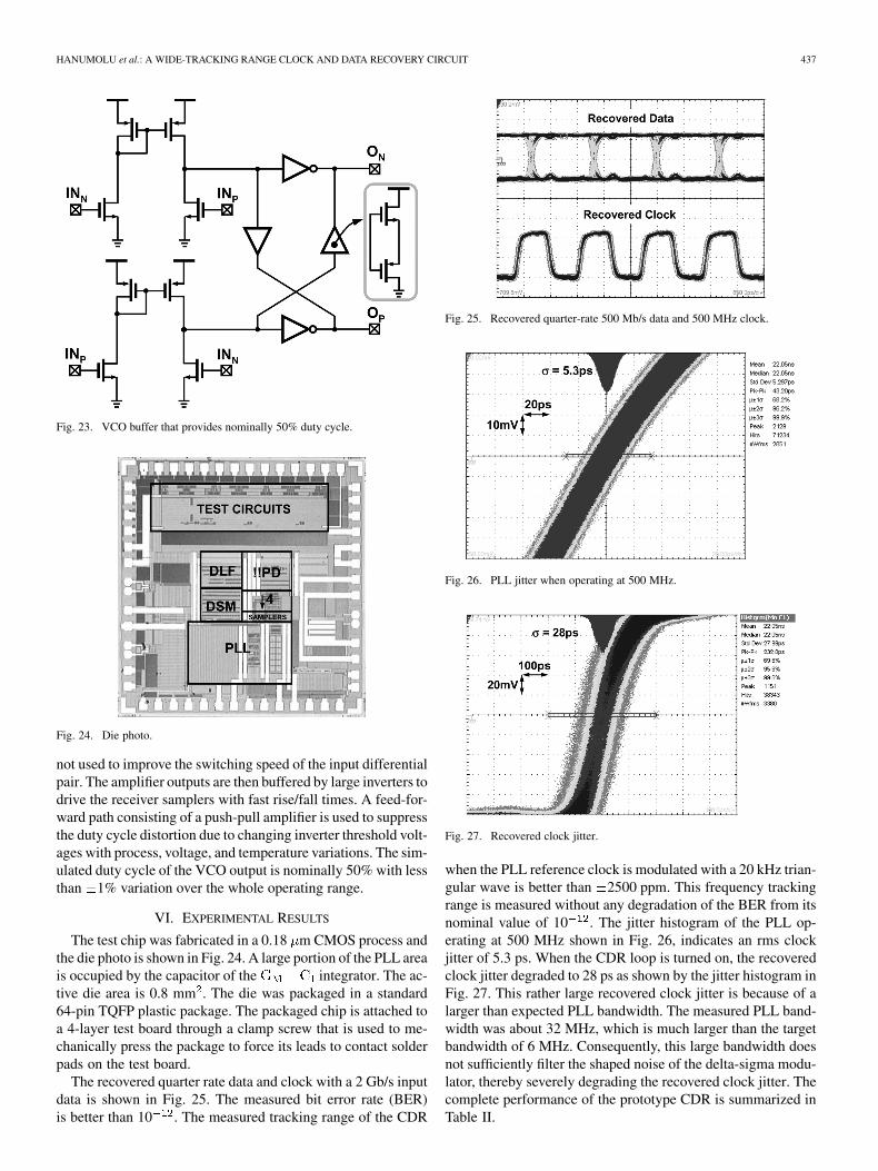
HANUMOLU et al.: A WIDE-TRACKING RANGE CLOCK AND DATA RECOVERY CIRCUIT 437
Fig. 23. VCO buffer that provides nominally 50% duty cycle.
Fig. 24. Die photo.
not used to improve the switching speed of the input differentialpair. The amplifier outputs are then buffered by large inverters todrive the receiver samplers with fast rise/fall times. A feed-for-ward path consisting of a push-pull amplifier is used to suppressthe duty cycle distortion due to changing inverter threshold volt-ages with process, voltage, and temperature variations. The sim-ulated duty cycle of the VCO output is nominally 50% with lessthan 1% variation over the whole operating range.
VI. EXPERIMENTAL RESULTS
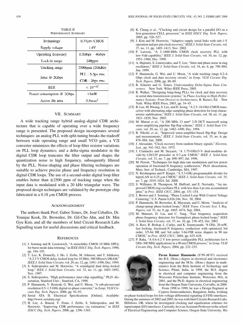
The test chip was fabricated in a 0.18 m CMOS process andthe die photo is shown in Fig. 24. A large portion of the PLL areais occupied by the capacitor of the integrator. The ac-tive die area is 0.8 mm . The die was packaged in a standard64-pin TQFP plastic package. The packaged chip is attached toa 4-layer test board through a clamp screw that is used to me-chanically press the package to force its leads to contact solderpads on the test board.
The recovered quarter rate data and clock with a 2 Gb/s inputdata is shown in Fig. 25. The measured bit error rate (BER)is better than 10 . The measured tracking range of the CDR
Fig. 25. Recovered quarter-rate 500 Mb/s data and 500 MHz clock.
Fig. 26. PLL jitter when operating at 500 MHz.
Fig. 27. Recovered clock jitter.
when the PLL reference clock is modulated with a 20 kHz trian-gular wave is better than 2500 ppm. This frequency trackingrange is measured without any degradation of the BER from itsnominal value of 10 . The jitter histogram of the PLL op-erating at 500 MHz shown in Fig. 26, indicates an rms clockjitter of 5.3 ps. When the CDR loop is turned on, the recoveredclock jitter degraded to 28 ps as shown by the jitter histogram inFig. 27. This rather large recovered clock jitter is because of alarger than expected PLL bandwidth. The measured PLL band-width was about 32 MHz, which is much larger than the targetbandwidth of 6 MHz. Consequently, this large bandwidth doesnot sufficiently filter the shaped noise of the delta-sigma modu-lator, thereby severely degrading the recovered clock jitter. Thecomplete performance of the prototype CDR is summarized inTable II.
438 IEEE JOURNAL OF SOLID-STATE CIRCUITS, VOL. 43, NO. 2, FEBRUARY 2008
TABLE IIPERFORMANCE SUMMARY
VII. SUMMARY
A wide tracking range hybrid analog–digital CDR archi-tecture that is capable of operating over a wide frequencyrange is presented. The proposed design incorporates severaltechniques: an analog PLL with split-tuning breaks the tradeoffbetween wide operating range and small VCO gain; a V2Iconverter minimizes the effects of loop filter resistor variationson PLL loop dynamics; and a delta-sigma modulator in thedigital CDR loop truncates the filter output and shapes thequantization noise to high frequency, subsequently filteredby the PLL. Noise-shaping and phase filtering techniques aresuitable to achieve precise phase and frequency resolution indigital CDR loops. The use of a second-order digital loop filterenables better than 2500 ppm of tracking range when theinput data is modulated with a 20 kHz triangular wave. Theproposed design techniques are validated by the prototype chipfabricated in a 0.18 m CMOS process.
ACKNOWLEDGMENT
The authors thank Prof. Gabor Temes, Dr. José Ceballos, Dr.Younjae Kook, Dr. Brownlee, Dr. Gil-Cho Ahn, and Dr. MinGyu Kim, and all the members of Intel Circuit Research LabsSignalling team for useful discussions and critical feedback.
REFERENCES
[1] J. Sonntag and R. Leonowich, “A monolithic CMOS 10 MHz DPLLfor burst-mode data retiming,” in IEEE ISSCC Dig. Tech. Papers, 1990,pp. 194–195.
[2] T. Lee, K. Donnelly, J. Ho, J. Zerbe, M. Johnson, and T. Ishikawa,“A 2.5 V CMOS delay-locked loop for 18 Mbit, 500 Mbyte/s DRAM,”IEEE J. Solid-State Circuits, vol. 29, no. 12, pp. 1491–1496, Dec. 1994.
[3] S. Sidiropoulos and M. Horowitz, “A semidigital dual delay-lockedloop,” IEEE J. Solid-State Circuits, vol. 32, no. 11, pp. 1683–1692,Nov. 1997.
[4] S. Sidiropoulos, “High performance inter-chip signalling,” Ph.D. dis-sertation, Stanford Univ., Stanford, CA, 1998.
[5] P. Hanumolu, V. Kratyuk, G. Wei, and U. Moon, “A sub-picosecondresolution 0.5–1.5 GHz digital-to-phase converter,” in Symp. VLSI Cir-cuits Dig. Tech. Papers, 2006, pp. 92–93.
[6] Serial ATA II: Electrical Specifications [Online]. Available:http://www.serialata.org/
[7] H. Lee, A. Bansal, Y. Frans, J. Zerbe, S. Sidiropoulos, and M.Horowitz, “Improving CDR performance via estimation,” in IEEEISSCC Dig. Tech. Papers, 2006, pp. 1296–1303.
[8] K. Chang et al., “Clocking and circuit design for a parallel I/O on afirst-generation CELL processor,” in IEEE ISSCC Dig. Tech. Papers,2005, pp. 526–527.
[9] J. Kim and M. Horowitz, “Adaptive supply serial links with sub-1-Voperation and per-pin clock recovery,” IEEE J. Solid-State Circuits, vol.37, no. 11, pp. 1403–1413, Nov. 2002.
[10] P. Larsson, “A 2–1600-MHz CMOS clock recovery PLL withlow-Vdd capability,” IEEE J. Solid-State Circuits, vol. 34, no. 12, pp.1951–1960, Dec. 1999.
[11] A. Hajimiri, S. Limotyrakis, and T. Lee, “Jitter and phase noise in ringoscillators,” IEEE J. Solid-State Circuits, vol. 34, no. 6, pp. 790–804,Jun. 1999.
[12] P. Hanumolu, G. Wei, and U. Moon, “A wide tracking range 0.2–4Gbps clock and data recovery circuit,” in Symp. VLSI Circuits Dig.Tech. Papers, 2006, pp. 88–89.
[13] R. Schreier and G. Temes, Understanding Delta-Sigma Data Con-verters. New York: Wiley-IEEE Press, 2005.
[14] R. Walker, “Designing bang-bang PLLs for clock and data recoveryin serial data transmission systems,” in Phase-Locking in High-Perfor-mance Systems: From Devices to Architectures, B. Razavi, Ed. NewYork: Wiley-IEEE Press, 2003, pp. 34–45.
[15] B. Lee, M. Hwang, S. Lee, and D. Jeong, “A 2.5–10-Gb/s CMOS trans-ceiver with alternating edge-sampling phase detection for loop charac-teristic stabilization,” IEEE J. Solid-State Circuits, vol. 38, no. 11, pp.1821–1829, Nov. 2003.
[16] M. Matsui et al., “A 200 MHz 13 mm 2-D DCT macrocell usingsense-amplifying pipeline flip-flop scheme,” IEEE J. Solid-State Cir-cuits, vol. 29, no. 12, pp. 1482–1490, Dec. 1994.
[17] B. Nikolic et al., “Improved sense-amplifier-based flip-flop: Designand measurements,” IEEE J. Solid-State Circuits, vol. 35, no. 6, pp.876–884, Jun. 2000.
[18] J. Alexander, “Clock recovery from random binary signals,” Electron.Lett., pp. 541–542, Oct. 1975.
[19] J. Craninckx and M. Steyaert, “A 1.75-GHz/3-V dual-modulus di-vide-by-128/129 prescaler in 0.7- m CMOS,” IEEE J. Solid-StateCircuits, vol. 31, no. 7, pp. 890–897, Jul. 1996.
[20] M. Perrott, “Techniques for high data rate modulation and low poweroperation of fractional-N frequency synthesizers,” Ph.D. dissertation,Mass. Inst. of Technol., Cambridge, MA, 1997.
[21] N. Krishnapura and P. Kinget, “A 5.3-GHz programmable divider forhiperLAN in 0.25- m CMOS,” IEEE J. Solid-State Circuits, vol. 35,no. 7, pp. 1019–1024, Jul. 2000.
[22] S. Williams, H. Thompson, M. Hufford, and E. Naviasky, “An im-proved CMOS ring oscillator PLL with less than 4 ps rms accumulatedjitter,” in Proc. IEEE CICC, 2004, pp. 151–154.
[23] J. Brown and J. Sonntag, “Phase Locked Loop With Control VoltageCentering,” U.S. Patent 6,826,246, Nov. 30, 2004.
[24] P. Hanumolu, M. Brownlee, K. Mayaram, and U. Moon, “Analysis ofcharge-pump phase-locked loops,” IEEE Trans. Circuits Syst. I, Reg.Papers, vol. 51, no. 9, pp. 1665–1674, Sep. 2004.
[25] M. Mansuri, D. Liu, and C. Yang, “Fast frequency acquisitionphase-frequency detectors for Gsamples/s phase-locked loops,” IEEEJ. Solid-State Circuits, vol. 37, no. 10, pp. 138–452, Oct. 2002.
[26] A. Ravi, R. Bishop, L. Carley, and K. Soumyanath, “8 GHz, 20 mW,fast locking, fractional-N frequency synthesizer with optimized 3rdorder, 3/5-bit IIR and 3rd order 3-bit-FIR noise shapers in 90 nmCMOS,” in Proc. IEEE CICC, 2004, pp. 625–628.
[27] P. Raha, “A 0.6-4.2 V low-power configurable PLL architecture for 6GHz-300 MHz applications in a 90 nm CMOS process,” in Symp. VLSICircuits Dig. Tech. Papers, 2004, pp. 232–235.
Pavan Kumar Hanumolu (S’99–M’07) receivedthe B.E. (Hons.) degree in electrical and electronicsengineering and the M.Sc. (Hons.) degree in math-ematics from the Birla Institute of Technology andScience, Pilani, India, in 1998, the M.S. degreein electrical and computer engineering from theWorcester Polytechnic Institute, Worcester, MA, in2001, and the Ph.D. degree in electrical engineeringfrom the Oregon State University, Corvallis, in 2006.
From 1998 to 1999, he was a Design Engineer atCypress Semiconductors, Bangalore, India, working
on phase-locked loops for low-voltage differential signaling (LVDS) interfaces.During the summers of 2002 and 2003, he was with Intel Circuits Research Labs,Hillsboro, OR, where he investigated clocking and equalization schemes forinput/output (I/O) interfaces. Currently, he is an Assistant Professor in the schoolof Electrical Engineering and Computer Science, Oregon State University. His
HANUMOLU et al.: A WIDE-TRACKING RANGE CLOCK AND DATA RECOVERY CIRCUIT 439
research interests include equalization, clock and data recovery for high-speedI/O interfaces, digital techniques to compensate for analog circuit imperfections,data converters, power-management circuits, and low-voltage mixed-signal cir-cuit design.
Dr. Hanumolu received the Analog Devices Outstanding Student DesignerAward in 2002, the Intel Ph.D. Fellowship in 2004, and was a co-recipient ofthe Custom Integrated Circuits Conference (CICC) 2006 Best Student PaperAward. He currently serves as an Associate Editor of the IEEE TRANSACTIONSON CIRCUITS AND SYSTEMS II, EXPRESS BRIEFS.
Gu-Yeon Wei received the B.S., M.S., and Ph.D. de-grees in electrical engineering from Stanford Univer-sity, Stanford, CA, in 1994, 1997, and 2001, respec-tively.
He is currently an Associate Professor of elec-trical engineering in the School of Engineering andApplied Sciences at Harvard University, Cambridge,MA. After a brief stint as a Senior Design Engineerat Accelerant Networks, Inc. in Beaverton, OR,he joined the faculty at Harvard as an AssistantProfessor in January 2002. His research interests
span several areas: high-speed, low-power link design; mixed-signal circuitsfor communications; ultra-low-power hardware for wireless sensor networks;and co-design of circuits and computer architecture for high-performance andembedded processors to address PVT variability and power consumption thatplague nanoscale CMOS technologies.
Un-Ku Moon (S’92–M’94–SM’99) received theB.S. degree from the University of Washington,Seattle, in 1987, the M.Eng. degree from CornellUniversity, Ithaca, NY, in 1989, and the Ph.D. degreefrom the University of Illinois at Urbana-Champaignin 1994, all in electrical engineering.
He has been with the School of Electrical Engi-neering and Computer Science, Oregon State Uni-versity, Corvallis, since 1998, where he is currentlya Professor. Before joining Oregon State University,he was with Bell Laboratories from 1988 to 1989,
and from 1994 to 1998. His technical contributions have been in the area ofanalog and mixed-signal circuits including highly linear and tunable contin-uous-time filters, telecommunication circuits including timing recovery and dataconverters, and ultra-low-voltage analog circuits for CMOS.
Prof. Moon is a recipient of the National Science Foundation CAREERAward and the Oregon State University’s Excellence in Graduate MentoringAward. He has served as an Associate Editor of the IEEE TRANSACTIONS ONCIRCUITS AND SYSTEMS II: ANALOG AND DIGITAL SIGNAL PROCESSING andon the Technical Program Committee of the IEEE Custom Integrated CircuitsConference. He currently serves as an Associate Editor of the IEEE JOURNALOF SOLID-STATE CIRCUITS and the Editor-in-Chief of the IEEE TRANSACTIONSON CIRCUITS AND SYSTEMS II: EXPRESS BRIEFS, and on the Technical ProgramCommittee of the IEEE VLSI Circuits Symposum and the Analog SignalProcessing Technical Committee of the IEEE Circuits and Systems Society. Healso serves on the IEEE Solid-State Circuits Society (SSCS) AdministrativeCommittee (AdCom) and the IEEE Circuits and Systems Society (CASS)Board of Governors (BoG) as the SSCS representative to CASS.