Embed Size (px)
Citation preview
A Wide Range PLL Research
for MIPI and SMIA Interface
at Mobile CMOS Image Sensor Applications
Sun-Yong Park
The Graduate School
Yonsei University
Department of Electrical and Electronic Engineering

A Wide Range PLL Research
for MIPI and SMIA Interface
at Mobile CMOS Image Sensor Applications
Master’s Thesis
Submitted to the Department of Electrical and Electronic Engineering
and the Graduate School of Yonsei University
in partial fulfillment of the requirements
for the degree of Master of Science
Sun-Yong Park
December 2009
This certifies that the master’s thesis of Sun-Yong Park is approved.
___________________________
Thesis Supervisor: Woo-Young Choi
___________________________
Gun-Hee Han
___________________________
Seong-Ook Jung
The Graduate School
Yonsei University
December 2009

iii
Contents Figure Index_____________________________________________ iv
Table Index _____________________________________________viii
Abstract ________________________________________________ix
1. Introduction____________________________________________1
2. Motivation and Research Background ______________________4 2-1. Interface at Mobile Image Sensor_______________________4 2-2. MIPI Interface______________________________________8 2-3. SMIA Interface____________________________________11
2-4. PLL basic fundamentals_____________________________12
3. Design of PLL_________________________________________20 3-1. Proposed PLL system diagram________________________20 3-2. Design of a Phase Frequency Detector________________22 3-3. Design of a Charge Pump ___________________________26 3-4. Design of a Wide Range Voltage Controlled Oscillator_____29 3-5. Design of a Frequency Divider________________________35
3-6. Degisn of a Loop Filter _____________________________38
4. IC Fabrication and Experiment Results______________________45 4-1. IC Fabrication_____________________________________45
4-2. Experiment Results_________________________________47
5. Conclusion___________________________________________57
Bibliography_____________________________________________59 Abstract (in Korean) ______________________________________62
iv
Figure Index
Figure 1.1 Function Block Diagram of Image Sensor______________2
Figure 2.1 Parallel Interface Diagram of Image Sensor_____________5
Figure 2.2 Output Bandwidth Trend of Image Sensor______________6
Figure 2.3 Serial Interface Diagram of Image Sensor______________7
Figure 2.4 CSI-2 Layer and PHY Layer Definition________________8
Figure 2.5 Structure of Data Land Physical Layer in Image Sensor__10
Figure 2.6 Block Diagram of a PLL___________________________12
Figure 2.7 Simple Charge Pump PLL Structure__________________13
Figure 2.8 Step Response of PFD / CP / LPF ___________________14
Figure 2.9 Linear Model of Simple Charge Pump PLL____________15
Figure 2.10 2ND
Figure 2.11 3
Order Charge Pump PLL______________________16
RD
Figure 3.1 Proposed Structure of PLL System___________________21
Order Charge Pump PLL______________________18
Figure 3.2 Implementation of Phase Frequency Detector__________22
v
Figure 3.3 Phase Frequency Detector, (a) Logic level circuit, (b)
Layout_________________________________________________24
Figure 3.4 Waveform of Phase Frequency Detector______________24
Figure 3.5 Dead Zone of Phase Frequency Detector______________25
Figure 3.6 Reset Time at Frequency matched___________________25
Figure 3.7 Charge Pump and Loop Filter Circuits________________26
Figure 3.8 Simulation of Current Mismatch____________________27
Figure 3.9 Transient Simulation of PFD / CP___________________28
Figure 3.10 Unit Differential Delay Cell, (a) Circuit, (b) Layout____30
Figure 3.11 Waveform of Differential Unit Delay Cell____________31
Figure 3.12 Structure of 4 Stage Differential Ring Osicllator_______32
Figure 3.13 Layout of 4 Stage Differential Ring Osicllator_______32
Figure 3.14 Simulation Result of VCO range, (a) -20 ℃, (b) 60 ℃__33
Figure 3.15 64 Divider Structure_____________________________35
Figure 3.16 2 Divider Circuit and Operation Sequence ________36
Figure 3.17 Layout of 64 Divider____________________________36

vi
Figure 3.18 Simulation Waveform of 64 Divider_________________37
Figure 3.19 Linear Model of Charge Pump PLL with N divider_____38
Figure 3.20 Bode Plot of Designed PLL Transfer Function, (a) Open
Loop, (b) Closed Loop_____________________________________41
Figure 3.21 Transient Simulation of Locking Time_______________42
Figure 3.22 Damping Split Bode Plot of PLL Transfer Function, (a)
Open Loop, (b) Closed Loop________________________________43
Figure 3.23 Transient Simulation of Control Voltage at Damping Split ,
(a) 0 ~ 4 us, (b) 3.6 ~ 3.85 us________________________________44
Figure 4.1 Layout of PLL Chip______________________________46
Figure 4.2 Layout of PLL Core______________________________46
Figure 4.3 Evaluation Board for Fabricated Chip________________47
Figure 4.4 Block Diagram of Test Environment_________________48
Figure 4.5 Test Setup Picture, (a) Spectrum Analyzer, (b) Digital
Oscilloscope_____________________________________________49
Figure 4.6 Measured VCO Frequency Range___________________51

vii
Figure 4.7 Frequency Error Rate between Simulation and Measurement
_______________________________________________________51
Figure 4.8 Real Picture of Power Spectrum at Locked, (a) Span 200
MHz, (b)Span 1 MHz MIPI mode, (c) Span 1 MHz SMIA mode__52
Figure 4.9 Measured Power Spectrum of PLL, (a) for MIPI, (b) for
SMIA__________________________________________________53
Figure 4.10 Measured Phase Noise of Frequency Synthesizer______54
Figure 4.11 Measured Waveform and Jitter, (a) Waveform at 1 GHz, (b)
Waveform at 650 MHz, (c) Jitter at 1 GHz, (d) Jitter at 650
MHz___________________________________________________55

viii
Table Index
Table 1. PLL Specification for MIPI and SMIA standard__________11
Table 2. Simulation Result of VCO Range_____________________34
Table 3. Loop Filter Constants_______________________________40
Table 4. Measurement Result of VCO Frequency Range __________50
Table 5. Measurement Summary _____________________________56
Table 6. Comparison with Performance of PLL _________________58

ix
Abstract
A Wide Range PLL Research
for MIPI and SMIA Interface
at Mobile CMOS Image Sensor Applications
By
Sun-Yong Park
Department of Electrical and Electronic Engineering
The Graduate School
Yonsei University
Recently, a mobile image sensors has high resolution image
quality by developing CMOS process technology and the output
bandwidth of the image sensor has increased, so it is classified to

x
support the standard interface as MIPI (Mobile Industry Processor
Interface) standard or SMIA (Standard Mobile Imaging Architecture)
standard. This these is a research about a low power and wide range
frequency synthesizer to generate high speed timing clock for MIPI and
SMIA standard serial interface which is used at high resolution mobile
CMOS image sensors.
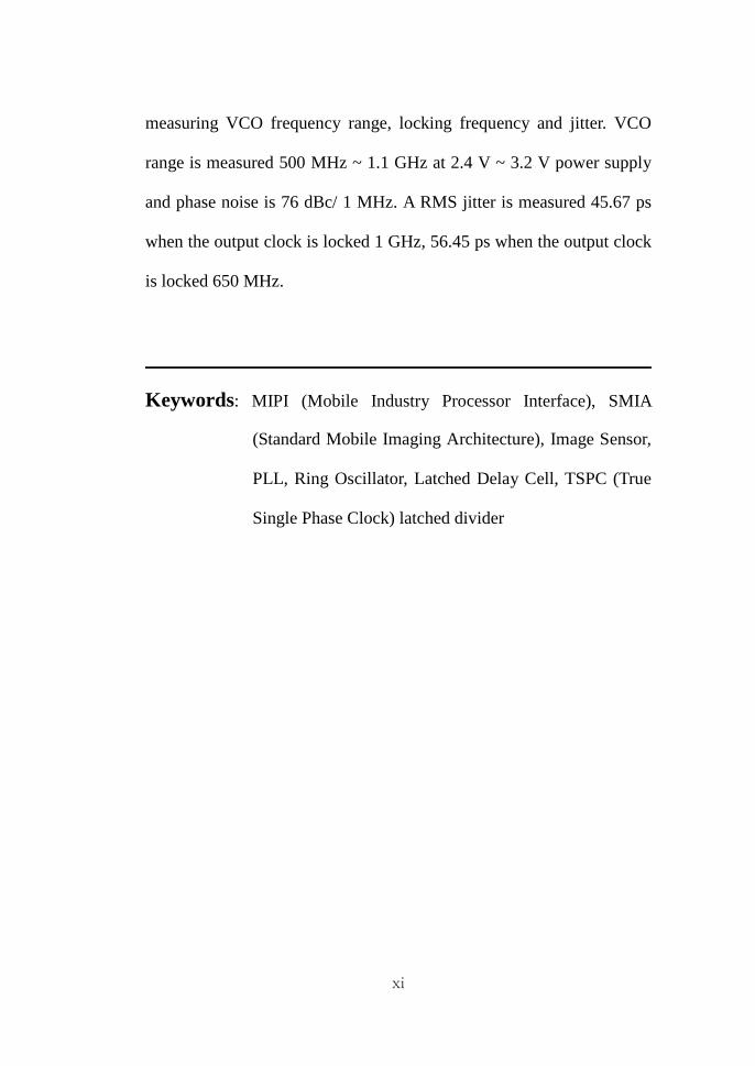
The designed frequency synthesizer uses 6 ~ 27 MHz external
reference clock and generates 1GHz output clock for MIPI standard
interface or 650MHz output clock for SMIA standard interface. The
output clock is 64 divided through TSPC (True single phase clock) type
divider to meet the bandwidth the output clock and the external
reference clock. A VCO (Voltage Controlled Oscillator) is designed 4
stage ring type by PMOS latched delay cell to operate well at process
variation, power supply and temperature variation to meet the MIPI and
SMIA standard specifications. This design is based on 0.18um CMOS
standard process, specially a 0.35 um thick gate oxide IO transistor is
used all circuit block to minimize the stand by current for mobile image
sensor. A frequency locking time is under 2.5 us and power
consumption is 20mW, when this frequency synthesizer operates at 1
GHz, 2.8 V power supply. The core area occupies 121 × 51 um2
The result of the designed frequency synthesizer is confirmed by
.

xi
measuring VCO frequency range, locking frequency and jitter. VCO
range is measured 500 MHz ~ 1.1 GHz at 2.4 V ~ 3.2 V power supply
and phase noise is 76 dBc/ 1 MHz. A RMS jitter is measured 45.67 ps
when the output clock is locked 1 GHz, 56.45 ps when the output clock
is locked 650 MHz.
Keywords: MIPI (Mobile Industry Processor Interface), SMIA
(Standard Mobile Imaging Architecture), Image Sensor,
PLL, Ring Oscillator, Latched Delay Cell, TSPC (True
Single Phase Clock) latched divider

1
Chapter Ⅰ
Introduction
1.1 Phase Locked Loop in Mobile CMOS image sensor
Lately, a mobile CMOS image sensor has been smaller and higher
resolution than before. Today, The minimum pixel size of 1.4 um ×
1.4 um is used at 5mega or 8mega mobile image sensor. A few years
ago, the past mobile image sensor had low resolution as 70 k ~ 1.3 M
pixels and there has parallel interface to transfer the output pixel data.
The output digital 10 bit or 12 bit data are sent to the receiver backend
chip through parallel interface. At the high resolution image sensor, the
output bandwidth is increased rapidly to send the amount of the 5mera
or 8mega pixel data. So, MIPI or SMIA serial interface is adapted at
commercial image sensor product and a frequency synthesizer in the
image sensor has to generate a 1 GHz clock for MIPI interface or a 650
MHz clock for SMIA interface.
Generally, 6 ~ 27 MHz external reference clock from a mobile set
board entered to a mobile image sensor and a phase locked loop in a
mobile image sensor generates internal clock for driving pixel arrays
and serializing the pixel output data.
2
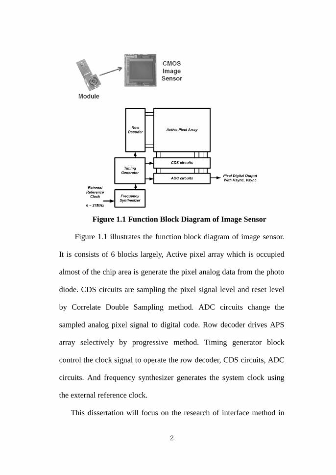
Figure 1.1 Function Block Diagram of Image Sensor
Figure 1.1 illustrates the function block diagram of image sensor.
It is consists of 6 blocks largely, Active pixel array which is occupied
almost of the chip area is generate the pixel analog data from the photo
diode. CDS circuits are sampling the pixel signal level and reset level
by Correlate Double Sampling method. ADC circuits change the
sampled analog pixel signal to digital code. Row decoder drives APS
array selectively by progressive method. Timing generator block
control the clock signal to operate the row decoder, CDS circuits, ADC
circuits. And frequency synthesizer generates the system clock using
the external reference clock.
This dissertation will focus on the research of interface method in
3
image sensors and the design and implementation of a frequency
synthesizer to meet the MIPI and SMIA interface standard in the high
resolution image sensors. At first, backgrounds of the interface of
image sensors will be explained, and then the basic operation of the
PLL and the loop dynamics will be described. Details of this
dissertation outline are as follows.
In chapter Ⅱ, Motivation and research background is discussed.
Section 2.1 introduces a interface of a image sensor. In section 2.2, the
MIPI interface standard will be shown in section 2.3 the SMIA
interface standard will be shown. And in section 2.4 describes the basic
of PLL and the loop dynamics.
Next, in chapter Ⅲ, the PLL design is described. At first, proposed
PLL is introduced in section 3.1. The designs of a phase frequency
detector, a charge pump circuits, a voltage controlled oscillator and
frequency divider are described in section 3.2 ~ 3.5. The design of a
loop filter is shown in section 3.6.
In chapter Ⅳ, IC fabrication and measurement are discussed. In
section 4.1, IC fabrication by 0.18um CMOS process is described, and
measurement results of fabricated chip are discussed in section 4.2.
At last, chapter Ⅴ summarizes results of the wide range PLL for
MIPI and SMIA interface at a mobile image sensor.
4
Chapter 2
Motivation and Research Background
2.1 The Interface of a Mobile Image Sensor
The pixel output data which are generated by the image sensor are
sent to the host backend chip for display or storage. First of all, the
output bandwidth (or the amount of the pixel output data) is calculated
below equation.
Output Bandwidth = Number of Horizontal pixels (include
Horizontal blank data) × Number of vertical pixels (include vertical
blank data) × 8bit ~ 12bit binary data of unit pixel × Number of
Frames/sec (2.1)
There are two types of the interfaces between mobile CMOS image
sensor and host for transmission of the pixel output data. One is
common parallel mode interface and the other is a serial mode interface.
A few years ago, we had used the mobile cellular phone which had
a camera and the resolution of that had 0.3mega pixels as VGA image
format. Also the pixel size of that image sensor is 3.5um × 3.5um.
5
The image data of the VGA camera system has about 100Mega
pixels binary data from the equation (2.1) that is operating at
15frames/sec, so the image data transmission is capable well at the
parallel mode interface.
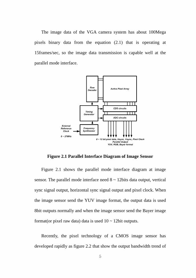
Figure 2.1 Parallel Interface Diagram of Image Sensor
Figure 2.1 shows the parallel mode interface diagram at image
sensor. The parallel mode interface need 8 ~ 12bits data output, vertical
sync signal output, horizontal sync signal output and pixel clock. When
the image sensor send the YUV image format, the output data is used
8bit outputs normally and when the image sensor send the Bayer image
format(or pixel raw data) data is used 10 ~ 12bit outputs.
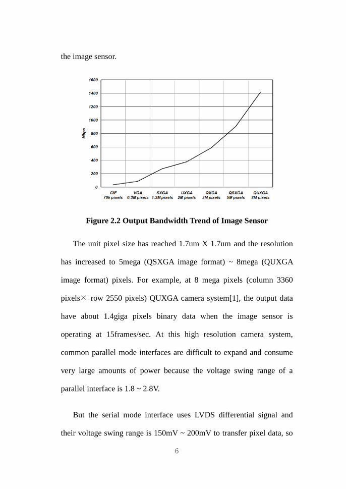
Recently, the pixel technology of a CMOS image sensor has
developed rapidly as figure 2.2 that show the output bandwidth trend of

6
the image sensor.
Figure 2.2 Output Bandwidth Trend of Image Sensor
The unit pixel size has reached 1.7um X 1.7um and the resolution
has increased to 5mega (QSXGA image format) ~ 8mega (QUXGA
image format) pixels. For example, at 8 mega pixels (column 3360
pixels× row 2550 pixels) QUXGA camera system[1], the output data
have about 1.4giga pixels binary data when the image sensor is
operating at 15frames/sec. At this high resolution camera system,
common parallel mode interfaces are difficult to expand and consume
very large amounts of power because the voltage swing range of a
parallel interface is 1.8 ~ 2.8V.
But the serial mode interface uses LVDS differential signal and
their voltage swing range is 150mV ~ 200mV to transfer pixel data, so

7
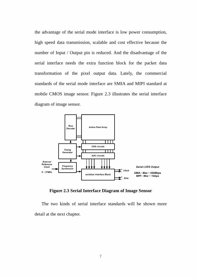
the advantage of the serial mode interface is low power consumption,
high speed data transmission, scalable and cost effective because the
number of Input / Output pin is reduced. And the disadvantage of the
serial interface needs the extra function block for the packet data
transformation of the pixel output data. Lately, the commercial
standards of the serial mode interface are SMIA and MIPI standard at
mobile CMOS image sensor. Figure 2.3 illustrates the serial interface
diagram of image sensor.
Figure 2.3 Serial Interface Diagram of Image Sensor
The two kinds of serial interface standards will be shown more
detail at the next chapter.
8
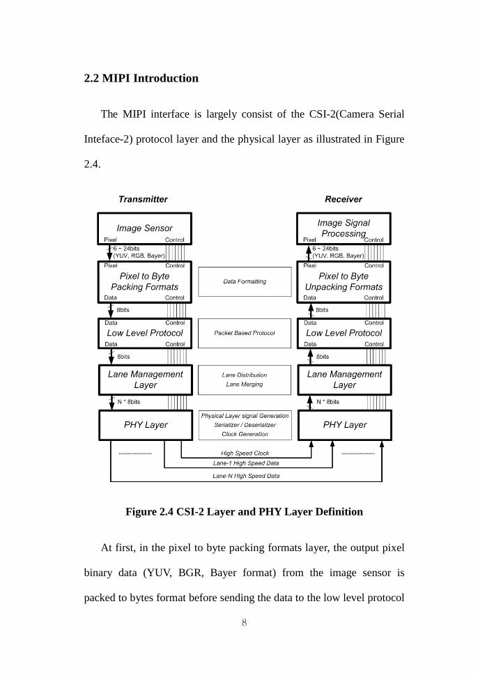
2.2 MIPI Introduction
The MIPI interface is largely consist of the CSI-2(Camera Serial
Inteface-2) protocol layer and the physical layer as illustrated in Figure
2.4.
Figure 2.4 CSI-2 Layer and PHY Layer Definition
At first, in the pixel to byte packing formats layer, the output pixel
binary data (YUV, BGR, Bayer format) from the image sensor is
packed to bytes format before sending the data to the low level protocol

9
layer. Also in the receiver (or host backend chip), this layer unpacks
bytes from the low level protocol layer into the original pixel data.
At the low level protocol layer, the received bytes data change
packet data form for serial data transmission. At the lane management
layer, the received packet data is distributed multi lane. This CSI-2
protocol is allowable the extension of the lane, so the lane may be one,
two, three or four depending on the output bandwidth requirements of
the application and the maximum bandwidth of the one lane is 1Gbps.
For example, in case of the 8mega image sensor, the output bandwidth
is needed about 1.4Gbps, so it is impossible to transfer the packet data
through only one lane. It may use the two lanes for the transmission of
the high resolution image packet data. Also in the receiver, this layer
recombines the each lane data stream.
At the physical layer, the separated packet data transfer the serial bit
stream through the LVDS (Low Voltage Differential Signal) form. In
LVDS mode, 0.2V common mode voltage at HS (High speed) mode,
1V common mode voltage at LP (Low Power), and their voltage swing
range is 0.2V.
Figure 2.5 shows the structure of data lane physical layer. It is
consist of the two data lanes driver and one clock lane driver. In master

10
IC or image sensor, PLL drives image sensor timing generator and
MIPI physical clock and data lane using external clock. And MIPI
clock and data lane transmitter send the LVDS signal. Slave IC or
image signal processor chip is getting the LVDS signal through MIPI
receiver [2], [3].
Figure 2.5 Structure of Data Lane Physical Layer in Image Sensor

11
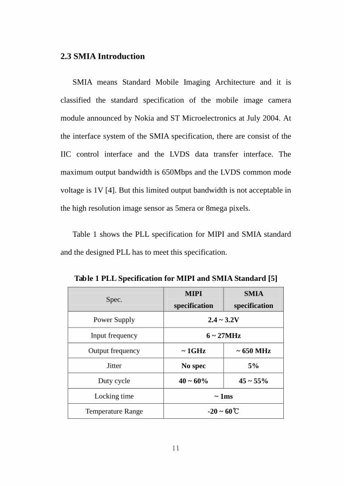
2.3 SMIA Introduction
SMIA means Standard Mobile Imaging Architecture and it is
classified the standard specification of the mobile image camera
module announced by Nokia and ST Microelectronics at July 2004. At
the interface system of the SMIA specification, there are consist of the
IIC control interface and the LVDS data transfer interface. The
maximum output bandwidth is 650Mbps and the LVDS common mode
voltage is 1V [4]. But this limited output bandwidth is not acceptable in
the high resolution image sensor as 5mera or 8mega pixels.
Table 1 shows the PLL specification for MIPI and SMIA standard
and the designed PLL has to meet this specification.
Table 1 PLL Specification for MIPI and SMIA Standard [5]
Spec. MIPI
specification SMIA
specification
Power Supply 2.4 ~ 3.2V
Input frequency 6 ~ 27MHz
Output frequency ~ 1GHz ~ 650 MHz
Jitter No spec 5%
Duty cycle 40 ~ 60% 45 ~ 55%
Locking time ~ 1ms
Temperature Range -20 ~ 60℃
12
2.4 PLL Basic Fundamentals
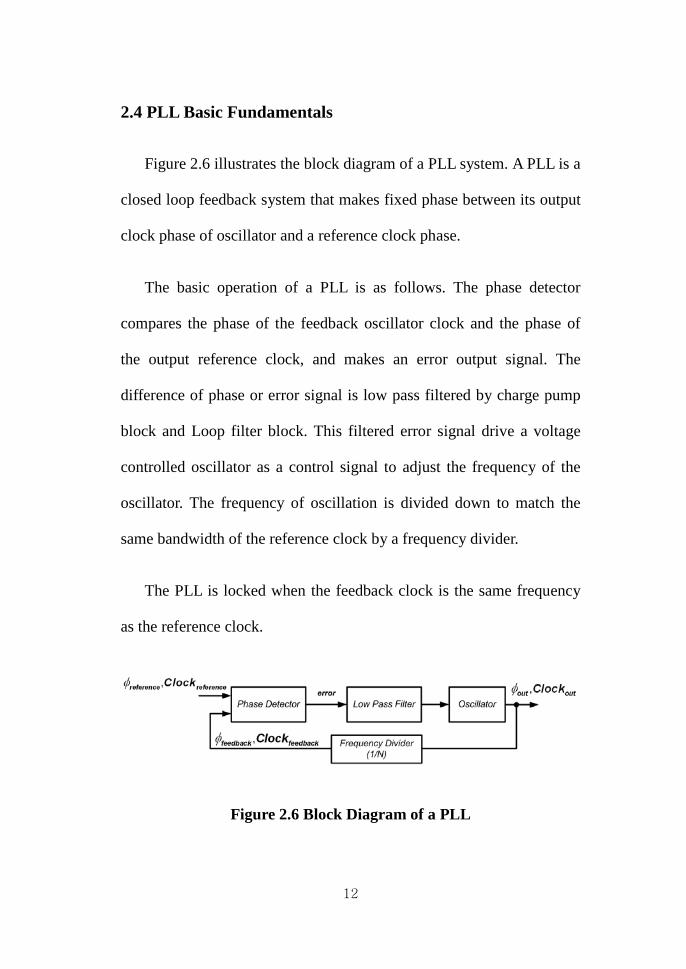
Figure 2.6 illustrates the block diagram of a PLL system. A PLL is a
closed loop feedback system that makes fixed phase between its output
clock phase of oscillator and a reference clock phase.
The basic operation of a PLL is as follows. The phase detector
compares the phase of the feedback oscillator clock and the phase of
the output reference clock, and makes an error output signal. The
difference of phase or error signal is low pass filtered by charge pump
block and Loop filter block. This filtered error signal drive a voltage
controlled oscillator as a control signal to adjust the frequency of the
oscillator. The frequency of oscillation is divided down to match the
same bandwidth of the reference clock by a frequency divider.
The PLL is locked when the feedback clock is the same frequency
as the reference clock.
Figure 2.6 Block Diagram of a PLL

13
2.4.1 Loop Dynamics in Charge Pump PLL
This section describes the dynamics of the Phase Locked Loop.
Figure 2.7 is called a charge pump PLL structure. The phase frequency
detector block is consist of two edge-triggered resettable D flip flops
with their D inputs tied to a logical one and the block detects the phase
or frequency differences and drives the charge pump accordingly. When
the ωout is far from ωin, the PFD and the charge pump change the
control voltage to approach ωin, also the input and output frequencies
are close, the PFD operates as a phase detector, so locks the phase.
Figure 2.7 Simple Charge Pump PLL Structure
In order to analysis the dynamic characteristic of the charge pump
PLL system, the components are created as a linear model to make the
transfer function [6].

14
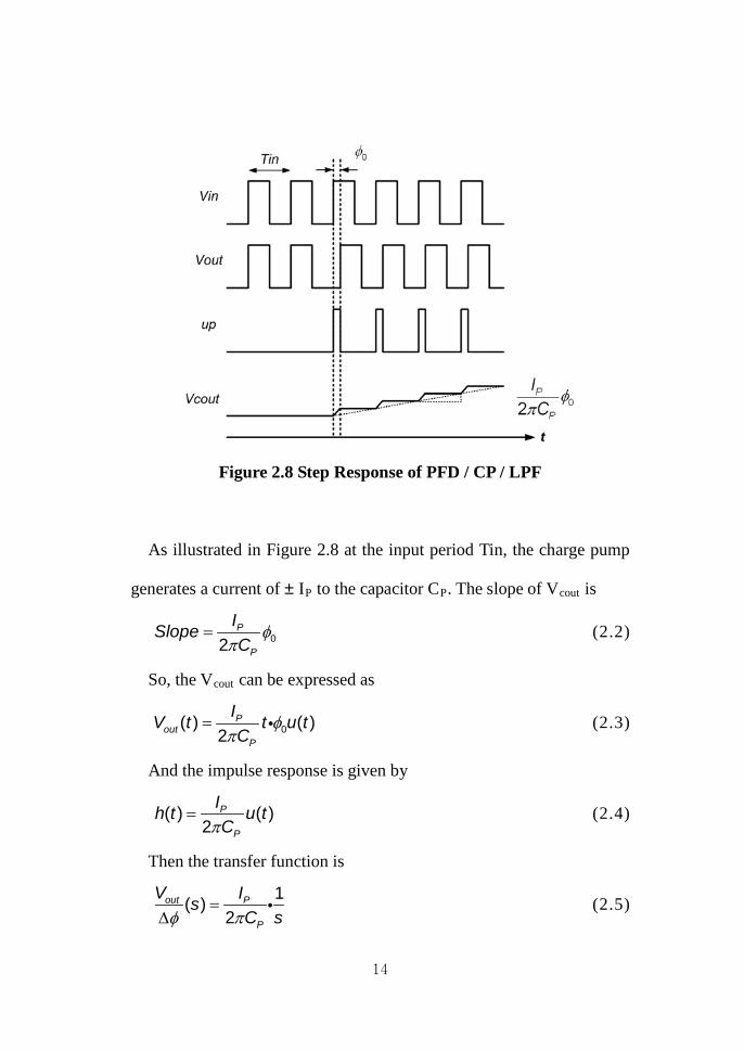
Figure 2.8 Step Response of PFD / CP / LPF
As illustrated in Figure 2.8 at the input period Tin, the charge pump
generates a current of ± IP to the capacitor CP. The slope of Vcout
02P
P
ISlopeC
φπ
=
is
(2.2)
So, the Vcout
0( ) ( )2
Pout
P
IV t t u tC
φπ
=
can be expressed as
(2.3)
And the impulse response is given by
( ) ( )2
P
P
Ih t u tCπ
= (2.4)
Then the transfer function is
1( )2
out P
P
V IsC sφ π
=∆
(2.5)
15
Also, the gain of phase frequency detector, KPFD
2P
PFDIKπ
=
is
(2.6)
2.4.2 Dynamics at Simple Charge Pump PLL
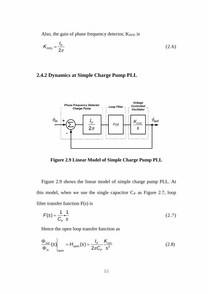
Figure 2.9 Linear Model of Simple Charge Pump PLL
Figure 2.9 shows the linear model of simple charge pump PLL. At
this model, when we use the single capacitor CP
1 1( )P
F sC s
=
as Figure 2.7, loop
filter transfer function F(s) is
(2.7)
Hence the open loop transfer function as
2( ) ( )2
out vcoPopen
in Popen
KIs H sC sπ
Φ= =
Φ (2.8)

16
And the closed loop transfer function as
2
22
( ) 2 2( )1 ( ) 1
2 2
VCO P VCOP
open P Pclosed
VCO P VCOPopen
P P
K I KIH s C s CH s K I KIH s s
C s C
π π
π π
= = =+ + +
(2.9)
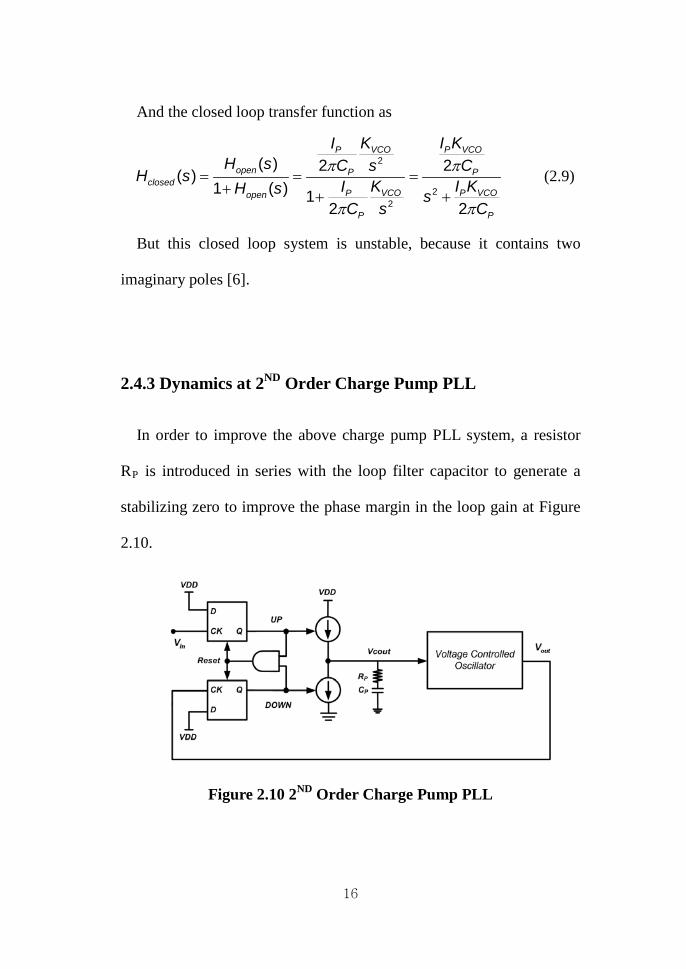
But this closed loop system is unstable, because it contains two
imaginary poles [6].
2.4.3 Dynamics at 2ND
In order to improve the above charge pump PLL system, a resistor
R
Order Charge Pump PLL
P is introduced in series with the loop filter capacitor to generate a
stabilizing zero to improve the phase margin in the loop gain at Figure
2.10.
Figure 2.10 2ND
Order Charge Pump PLL

17
And the modified loop filter transfer function as
1( ) ( )PP
F s RC s
= + (2.10)
Hence the open loop transfer function as
1( ) ( ) ( )2
out vcoPopen P
in Popen
KIs H s RC s sπ
Φ= = +
Φ (2.11)
And the closed loop transfer function as
1( )( ) 2( )11 ( ) 1 ( )
2
vcoPP
open Pclosed
vcoPopenP
P
KI RH s C s sH s KIH s RC s s
π
π
+= =
+ + +
2
( 1)2
2 2
P VCOP P
P
P VCO P VCOP
P
I K R C sC
I K I Ks R sC
π
π π
+=
+ + (2.12)
At this 2ND order charge pump PLL system, the charge pump drives
the series resistor RP and capacitor CP
, so a current is injected into the
loop filter at each period time. This cause the large jumping voltage to
the control voltage and even in the locked condition, the mismatches
between charge current and discharge current of the charge pump and
the clock feed-through of the charge pump switches cause the jumping
voltage also. This ripple modulates the frequency of the voltage
controlled oscillator and introduces excessive jitter [6].

18
2.4.4 Dynamics at 3RD
In order to improve the 2
Order Charge Pump PLL
ND order charge pump PLL system, a small
capacitor is added in parallel with resistor RP and capacitor CP
loop
filter network as shown in Figure 2.11 to suppress the ripple induced
jitter in the output voltage.
Figure 2.11 3RD
But this capacitor C
Order Charge Pump PLL
S
The modified loop filter transfer function as
generates a pole, so increasing the order of the
charge pump PLL system to three and the phase degradation due to this
pole.
1
( ) 1( )P P
SP P S
sR CF s
C s sR C C
+=
+
(2.13)
19
Hence the open loop transfer function as
1
( ) ( ) 12 ( )out vcoP P P
openin open S
P P S
sKI R Cs H s
sC s sR C C
π
+Φ
= =Φ +
(2.14)
And the closed loop transfer function as
1
12 ( )( )( ) 11 ( )
1 12 ( )
vcoP P P
Sopen P P S
closedopen
vcoP P P
SP P S
sKI R C
sC s sH s R C CH sH s s
KI R CsC s s
R C C
π
π
+
+= =
+ ++
+
3 2
1( )2
1( )2 2
P VCO
S P P
P VCO P VCO
P P S S P P S
I K sC R C
I K I Ks s sR C C C R C C
π
π π
+=
+ + +
(2.15)
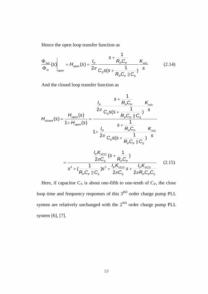
Here, if capacitor CS is about one-fifth to one-tenth of CP, the close
loop time and frequency responses of this 3RD order charge pump PLL
system are relatively unchanged with the 2ND order charge pump PLL
system [6], [7].

20
CHAPTER 3
Design of PLL
3.1 Proposed PLL System Diagram
Recently, the fabrication of standard CMOS process technologies
has been developed rapidly, and gate length reach to 32nm. But this fast
CMOS transistor is not acceptable to use mobile image sensors,
because of the leakage issue of transistor. For low operating power
consumption and minimization of stand-by power consumption, mobile
image sensors are designed by thick gate oxide transistor for analog
circuits and pixels except digital logic circuits which are used thin gate
oxide transistor. And analog power supply is used 2.8V for reduction of
operating power consumption. So, proposed PLL is designed by thick
gate oxide transistor for all circuit blocks and used 2.8V as power
supply voltage.
Figure 3.1 shows that designed PLL system overall diagram. The
phase frequency detector make up and down error pulses based on the
phase and frequency difference between the input reference clock and
divided feedback clock. The up and down error pulses drive charge
pumping switches to charge or discharge of loop filter components.
And the output voltage of loop filter controls the frequency of the
21
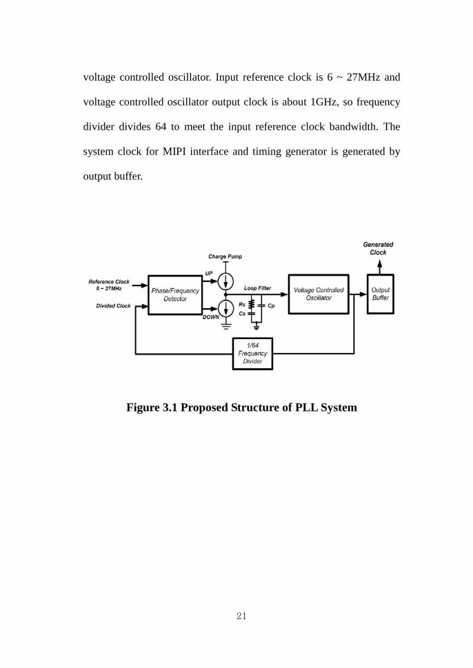
voltage controlled oscillator. Input reference clock is 6 ~ 27MHz and
voltage controlled oscillator output clock is about 1GHz, so frequency
divider divides 64 to meet the input reference clock bandwidth. The
system clock for MIPI interface and timing generator is generated by
output buffer.
Figure 3.1 Proposed Structure of PLL System
22
3.2 The Design of a Phase Frequency Detector
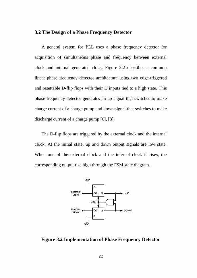
A general system for PLL uses a phase frequency detector for
acquisition of simultaneous phase and frequency between external
clock and internal generated clock. Figure 3.2 describes a common
linear phase frequency detector architecture using two edge-triggered
and resettable D-flip flops with their D inputs tied to a high state. This
phase frequency detector generates an up signal that switches to make
charge current of a charge pump and down signal that switches to make
discharge current of a charge pump [6], [8].
The D-flip flops are triggered by the external clock and the internal
clock. At the initial state, up and down output signals are low state.
When one of the external clock and the internal clock is rises, the
corresponding output rise high through the FSM state diagram.
Figure 3.2 Implementation of Phase Frequency Detector
23
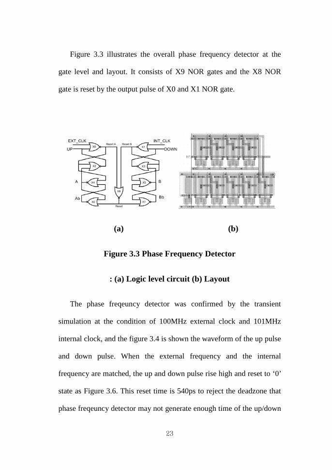
Figure 3.3 illustrates the overall phase frequency detector at the
gate level and layout. It consists of X9 NOR gates and the X8 NOR
gate is reset by the output pulse of X0 and X1 NOR gate.
(a) (b)
Figure 3.3 Phase Frequency Detector
: (a) Logic level circuit (b) Layout
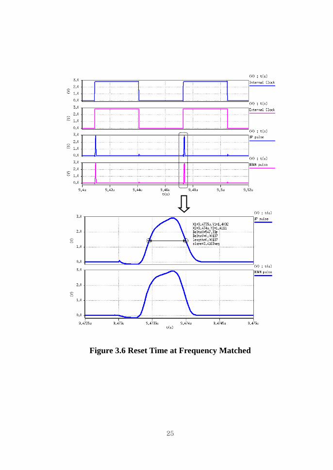
The phase freqeuncy detector was confirmed by the transient
simulation at the condition of 100MHz external clock and 101MHz
internal clock, and the figure 3.4 is shown the waveform of the up pulse
and down pulse. When the external frequency and the internal
frequency are matched, the up and down pulse rise high and reset to ‘0’
state as Figure 3.6. This reset time is 540ps to reject the deadzone that
phase freqeuncy detector may not generate enough time of the up/down

24
pulse to swtich of the charge pump in the small phase difference. If
deadzone occures in the phase frequency detector, the loop gain is zero,
then the output phase isn’t locked and generate the jitter. Figure 3.5
illustrates the daedzone simulation of phase frequency detector.
Figure 3.4 Waveform of Phase Frequency Detector
Figure 3.5 Dead Zone of Phase Frequency Detector
25
Figure 3.6 Reset Time at Frequency Matched

26
3.3 The Design of a Charge Pump
A charge pump block generates the current to drive the control
voltage of the voltage controlled oscillator. When the up pulse is
generated from the phase frequency detector, the current charges the
loop filter and when the down pulse is generated from the phase
frequency detector, the current discharges the loop filter. At this point,
the mismatch of the charge current and the discharge current and each
leakage current cause the static phase error when the PLL system is
locked. This periodical charge pump operation for compensation of this
error makes the high frequency harmonics at the control voltage, and it
generates a jitter [9].
To reduce the mismatch current, the charge pump circuit is used the
feedback amplifier as Figure 3.7.
Figure 3.7 Charge pump and Loop Filter Circuits

27
At this charge pump circuit, the transistors size of the left current
path is the same as the right current path and the voltage of the ‘ref’
node is the same voltage as the ‘vf’ node through the feedback
operation of the amplifier. Figure 3.8 show the current mismatch of this
charge pump circuit. When the up and down pulse enter the charge
pump circuit, ‘vf’ node is sweeped voltage from gnd to vdd to measure
the charge current and the discharge current. From the simulation result,
charge pump current ‘IP’ is 58 ~ 65uA at 2.8V power supply voltage
and this range is used to drive the control voltage. And mismatch
current is 2.1uA at 0.5V control voltage, 99nA at 2V control voltage.
Figure 3.8 Simulation of Current Mismatch

28
Figure 3.9 shows the overall transient waveform of phase freqeuncy
detector and charge pump circuit. When internal clock is faster than
external clock, down pulse is generated and charge pump current is
discharged, “vf” node slow down. And external clock is faster than
internal clock, up pulse is generated and charge pump current is
chraged, “vf” node rise up.
Figure 3.9 Transient Simulation of PFD / CP

29
3.4 The Design of a Wide Range Voltage Controlled Oscillator
Generally the method of the design of voltage controlled oscillator
is largely LC oscillator and ring type oscillator at the standard CMOS
process. LC oscillator is very stable and low phase noise to generate
clock, but an inductor component in LC oscillator occupies large area
and is difficult to design. But ring type oscillator has the advantage of a
simple structure, a wide frequency range and designable small area. So
ring type oscillator is adapted at a wide range PLL for a mobile image
sensor. Ring oscillator has a delay cell to generate time delay and the
delay cell has two types. One is single ended inverter, but this delay cell
is poor quality to generate a constant frequency, because it has a poor
power supply rejection ratio. Another is differential delay cell which is
less sensitive to common mode voltage variation, such as supply noise
fluctuation [10].
Figure 3.10 illustrates the differential delay cell which is adapted at
this PLL system. Diode connected transistor M3, M4 are operating as a
load resistor at linear region. The cross coupled transistor M5, M6 are
speed up the transition of the output signal as working like latch, so the
delay cell is insensitive to power supply variation [11],[12].

30
(a)
(b)
Figure 3.10 Unit Differential Delay Cell
: (a) Circuit (b) Layout
31
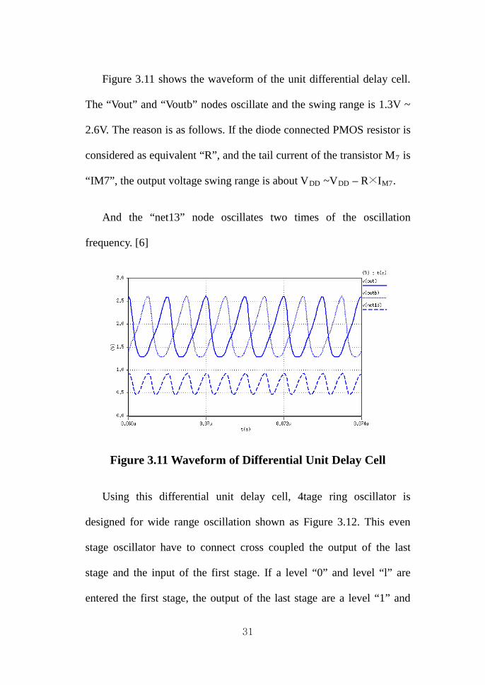
Figure 3.11 shows the waveform of the unit differential delay cell.
The “Vout” and “Voutb” nodes oscillate and the swing range is 1.3V ~
2.6V. The reason is as follows. If the diode connected PMOS resistor is
considered as equivalent “R”, and the tail current of the transistor M7 is
“IM7”, the output voltage swing range is about VDD ~VDD – R×IM7
And the “net13” node oscillates two times of the oscillation
frequency. [6]
.
Figure 3.11 Waveform of Differential Unit Delay Cell
Using this differential unit delay cell, 4tage ring oscillator is
designed for wide range oscillation shown as Figure 3.12. This even
stage oscillator have to connect cross coupled the output of the last
stage and the input of the first stage. If a level “0” and level “l” are
entered the first stage, the output of the last stage are a level “1” and
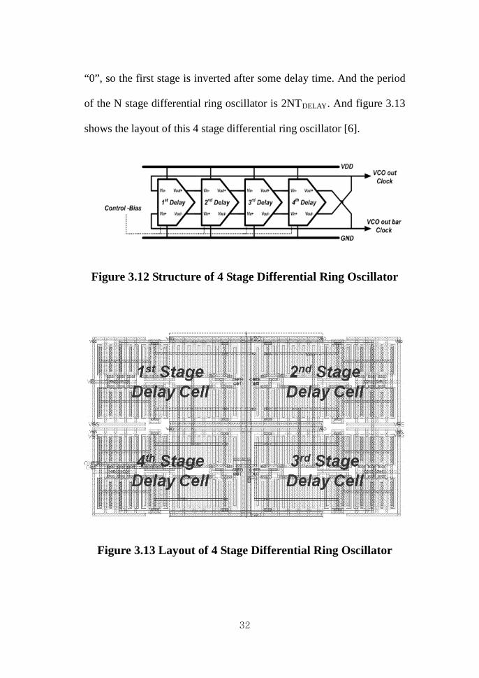
32
“0”, so the first stage is inverted after some delay time. And the period
of the N stage differential ring oscillator is 2NTDELAY. And figure 3.13
shows the layout of this 4 stage differential ring oscillator [6].
Figure 3.12 Structure of 4 Stage Differential Ring Oscillator
Figure 3.13 Layout of 4 Stage Differential Ring Oscillator

33
0.0 0.5 1.0 1.5 2.0 2.5200
400
600
800
1000
1200
1400
1600
1800
2000
VCO
Fre
quen
cy [M
Hz]
Control Voltage [V]
FF Corner FS Corner TT Corner SF Corner SS Corner
(a) -20℃
0.0 0.5 1.0 1.5 2.0 2.5200
400
600
800
1000
1200
1400
1600
1800
VCO
Fre
quen
cy [M
Hz]
Control Voltage [V]
FF Corner FS Corner TT Corner SF Corner SS Corner
(b) 60℃
Figure 3.14 Simulation Result of VCO Range
: (a) -20℃ (b) 60℃
34
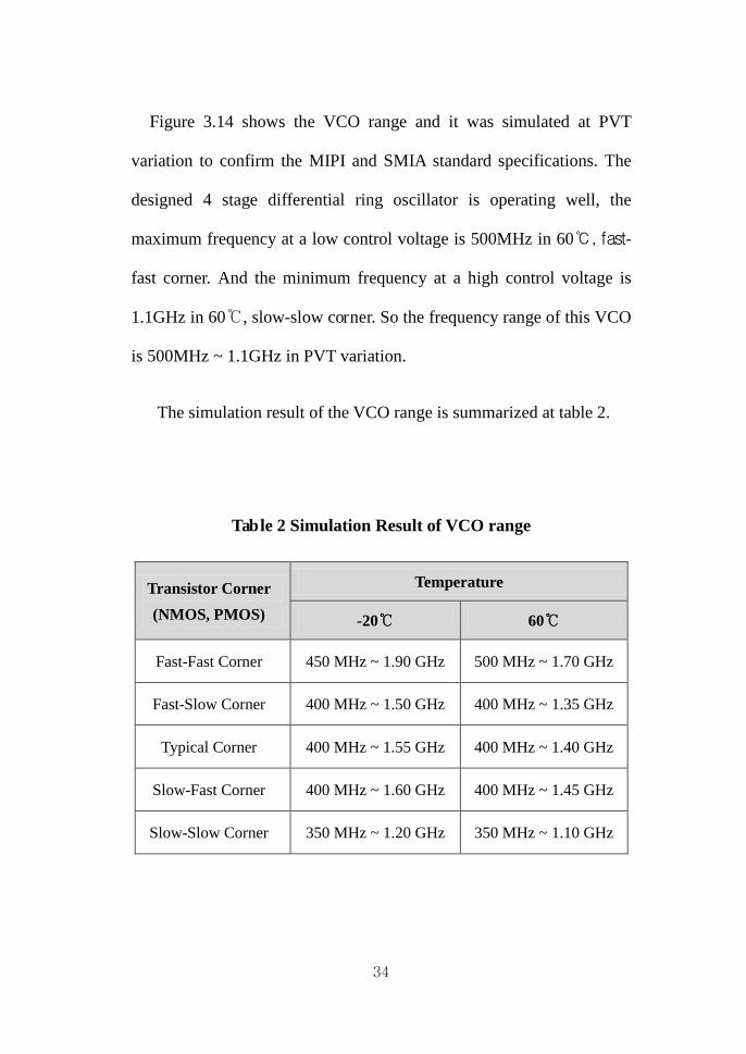
Figure 3.14 shows the VCO range and it was simulated at PVT
variation to confirm the MIPI and SMIA standard specifications. The
designed 4 stage differential ring oscillator is operating well, the
maximum frequency at a low control voltage is 500MHz in 60℃, fast-
fast corner. And the minimum frequency at a high control voltage is
1.1GHz in 60℃, slow-slow corner. So the frequency range of this VCO
is 500MHz ~ 1.1GHz in PVT variation.
The simulation result of the VCO range is summarized at table 2.
Table 2 Simulation Result of VCO range
Transistor Corner (NMOS, PMOS)
Temperature
-20℃ 60℃
Fast-Fast Corner 450 MHz ~ 1.90 GHz 500 MHz ~ 1.70 GHz
Fast-Slow Corner 400 MHz ~ 1.50 GHz 400 MHz ~ 1.35 GHz
Typical Corner 400 MHz ~ 1.55 GHz 400 MHz ~ 1.40 GHz
Slow-Fast Corner 400 MHz ~ 1.60 GHz 400 MHz ~ 1.45 GHz
Slow-Slow Corner 350 MHz ~ 1.20 GHz 350 MHz ~ 1.10 GHz

35
3.5 The Design of a Frequency Divider
At a mobile image sensor, the reference system clock needs a low
frequency about 6 ~ 27MHz, and a clock generator of the mobile image
sensor need above 1GHz frequency clock to support the MIPI interface
function. So it is designed a 64 divider for match the reference input
clock and the 1GHz high frequency system clock as shown figure 3.15.
Figure 3.15 64 Divider Structure
At a typical complementary static logic D flip flop, there are many
transistor path from the input node to the output node and the signal
delay increases, so the speed of the static D flip flop is limited. In this
PLL, the maximum frequency output clock of the voltage controlled
oscillator is about 1.9GHz from the simulation result of a PVT variation.
So the static logic D flip flop is not acceptable.
A TSPC (True Single Phase Clock) type dynamic logic D flip flop
is used for 2-divider at this PLL shown as figure 3.16 [13].

36
Figure 3.16 2 Divider Circuit and Operation Sequence
This divider called negative edge triggered register that consists of
positive latch and negative latch. At the operation sequence of figure
3.16, the negative edge clock is entered to this divider, the output Q
node latches the value of B node, so the entered clock is divided by 2.
Figure 3.17 Layout of 64 Divider

37
Figure 3.17 shows the layout of the 64-divider, and figure 3.18
shows the simulation result of the frequency at each divider output
node and the simulation waveform of the 64-divider. When the VCO
output frequency is 1GHz, the output frequency of the 64 divider is
15.625MHz.
Figure 3.18 Simulation Waveform of 64 Divider

38
3.6 The Design of a Loop Filter
The design of a loop filter is important as the stability and the
locking quality of a PLL system [9]. To stabilize the PLL system, it is
used a conventional 3rd
Figure 3.19 shows the linear model of a charge pump PLL with N
divider.
order loop filter. First of all, to achieve the
optimal value of a loop filter components register and capacitor, it is
calculated by the next equation.
Figure 3.19 Linear Model of Charge Pump PLL with N
divider
At this charge pump PLL with N divider, the closed loop transfer
function is modified from the equation (2.11) with N. So the closed
loop transfer function is

39
1( )( ) 2( ) 1 11 ( ) 1 ( )2
π
π
+= =
+ + +
vcoPP
open Pclosed
vcoPopen P
P
KI RH s C s sH s KIH s RN N C s s
(3.1)
And this equation can be the next form through the control theory.
2
2 2
22ζω ωζω ω
+=
+ +n n
n n
ss s
(3.2)
Hence, the Capacitor Cp and the register RP
22π ω=
vcoPP
n
KICN
is
(3.3)
4πζω= n
PP VCO
RI K
(3.4)
10= P
NCC (3.5)
Where IP is a charge pump current, N is a dividing factor, KVCO is a
VCO gain and each value is used by the simulation result shown as
Table 3. And the natural frequency (or the loop bandwidth) ωN should
be smaller than 1/10 of the reference frequency for the system stability.
In this work, input reference frequency is 15.6 MHz for MIPI interface,
and 10.15 MHz for SMIA interface, so the loop bandwidth ωN value is
selected about 8M rad/sec. The damping ratio ζ is 1 to get a fast

40
locking time. From these constants, the resistor RP is 12 kΩ from the
equation (3.3), the series capacitor CP is 34 pF from the equation (3.4),
and the shunt capacitor CS
Table 3 Loop filter Constants
is 3.4 pF from the equation (3.5).
Constants Value
KVCO (VCO Gain) 810 MHz
IP (Charge Pump Current) 65 uA
Input Reference Frequency 15.625 MHz
ωN (Natural Frequency or loop bandwidth) 8M rad/sec
Division 64
ζ (Damping Ratio) 1
CP (Loop Parallel Capacitor) 34 pF
RP (Loop Parallel Resistor) 12 kΩ
Cs (Loop shunt Capacitor) 3.4 pF
The designed loop filter parameter is confirmed through MATLAB
procedure, and the result of figure 3.20(a) is open loop bode diagram of
this 3RD order charge pump PLL, and figure 3.20(b) is closed loop bode
diagram of this 3RD order charge pump PLL. Generally speaking, phase
margin is good in 45˚ ~ 60˚ to make the loop steadily [14]. At figure

41
3.20(a), the gain intersection is corresponding with peak value of phase
response curve, and the peak value is 56˚ to stabilize this system.
(a)
(b)
Figure 3.20 Bode Plot of Designed PLL Transfer Function
: (a) Open loop (b) Closed loop
ΦM=56˚
ωN=8M rad/sec

42
Finally transient simulation was carried out over all PLL block with
the selected loop parameter as shown figure 3.21. 1 GHz clock PLL
output was locked about 1.5 us for MIPI clock at 0.627 V control
voltage and 650 MHz clock PLL output was locked about 2.5 us for
SMIA clock at 0.25 V control voltage.
Figure 3.21 Transient Simulation of Locking Time
If a damping ratio control the locking time and stability in the PLL
system. Figure 3.22 illustrates the bode plot of damping ratio splits
through MATLAB. When the damping ratio rises, the loop bandwidth

43
is reduced in the open loop transfer function, and magnitude rises in the
closed loop transfer function.
(a)
(b)
Figure 3.22 Damping Split Bode Plot of PLL Transfer
Function : (a) Open loop (b) Closed loop

44
At figure 3.23, when the damping ratio is over “1”, the PLL system
is unstable. But, when the damping ratio is “0.707” or “1”, the PLL
system is locked stable. The locking time of the damping ratio “1” is
faster than that of “0.707”.
(a)
(b)
Figure 3.23 Transient Simulation of Control Voltage at Damping Split : (a) 0 ~ 4us (b) 3.6 ~ 3.85us

45
CHAPTER Ⅳ
IC Fabrication and Experiment Results
4.1 IC Fabrication
A proposed PLL for MIPI and SMIA interface was fabricated
using a Dongbu 0.18-μm mixed signal process technology. As it is
mentioned chater2, it is designed by using the thick gate oxide
transistor that minimum gate length is 0.35um of thick gate oxide
transistor to reduce the standby current. Figure 4.1 shows the fabricated
chip, and there are MOS decoupling capacitor for reduce power supply
noise in the vacancy chip area.
And figure 4.2 shows the core layout of the designed PLL and
occupies the area of 121 x 51 um2
.

46
Figure 4.1 Layout of the PLL chip
Figure 4.2 Layout of the PLL core

47
4.2 Experiment Results
4.2.1 Printed Circuit Board Design
Figure 4.3 shows the evaluation board for fabricated chip. At the
printed circuit board, selector switch is used when the fabricated chip is
measured for evaluation of the PLL function or the VCO frequency
range. And the variable resistor controls the VCO control voltage for
measurement of the VCO frequency range when the evaluation board is
VCO measurement mode.
Figure 4.3 Evaluation Boards for Fabricated Chip
Variable Resistor
Power Supply
Selector Switch
Loop Filter
Fabricated Chip
Reference Clock Input
VCO Clock Output
48
4.2.2 Test Setup
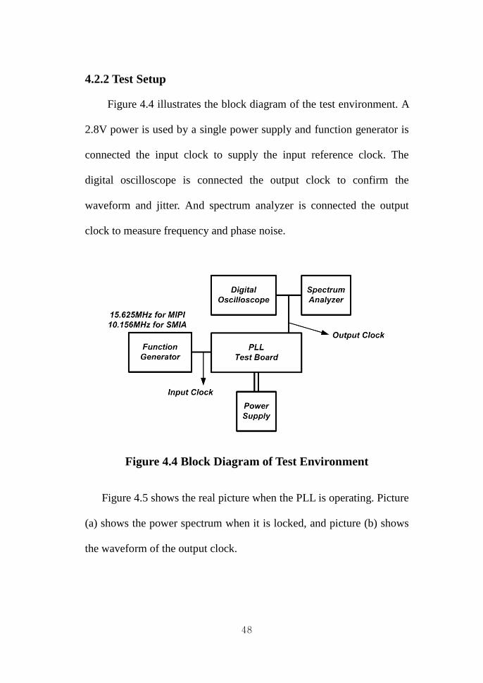
Figure 4.4 illustrates the block diagram of the test environment. A
2.8V power is used by a single power supply and function generator is
connected the input clock to supply the input reference clock. The
digital oscilloscope is connected the output clock to confirm the
waveform and jitter. And spectrum analyzer is connected the output
clock to measure frequency and phase noise.
Figure 4.4 Block Diagram of Test Environment
Figure 4.5 shows the real picture when the PLL is operating. Picture
(a) shows the power spectrum when it is locked, and picture (b) shows
the waveform of the output clock.

49
(a)
(b)
Figure 4.5 Test Setup Picture
: (a) Spectrum Analyzer (b) Digital Oscilloscope
Digital Oscilloscope
Power Supply Function
Generator Evaluation
Board
Spectrum Analyzer
Function Generator
Power Supply
Evaluation Board
50
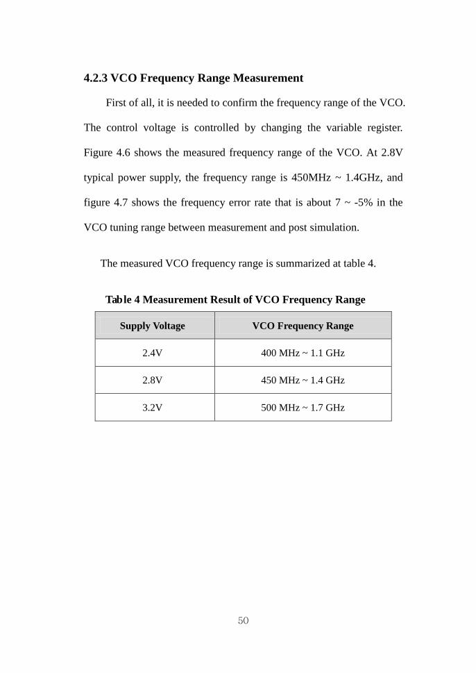
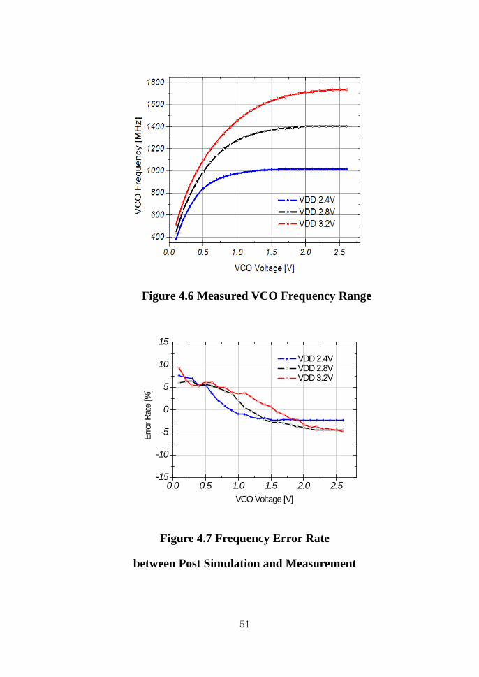
4.2.3 VCO Frequency Range Measurement
First of all, it is needed to confirm the frequency range of the VCO.
The control voltage is controlled by changing the variable register.
Figure 4.6 shows the measured frequency range of the VCO. At 2.8V
typical power supply, the frequency range is 450MHz ~ 1.4GHz, and
figure 4.7 shows the frequency error rate that is about 7 ~ -5% in the
VCO tuning range between measurement and post simulation.
The measured VCO frequency range is summarized at table 4.
Table 4 Measurement Result of VCO Frequency Range
Supply Voltage VCO Frequency Range
2.4V 400 MHz ~ 1.1 GHz
2.8V 450 MHz ~ 1.4 GHz
3.2V 500 MHz ~ 1.7 GHz
51
Figure 4.6 Measured VCO Frequency Range
0.0 0.5 1.0 1.5 2.0 2.5-15
-10
-5
0
5
10
15
Erro
r Rat
e [%
]
VCO Voltage [V]
VDD 2.4V VDD 2.8V VDD 3.2V
Figure 4.7 Frequency Error Rate
between Post Simulation and Measurement

52
4.2.4 PLL Measurement
The locked frequency is confirmed by spectrum analyzer. Figure
4.8 shows the real picture when it is locked at 1GHz, the component of
the input reference clock 15.625MHz is shown as side spur in figure (a).
And figure 4.9 shows power spectrum at 15.6MHz span.
(a)
(b) (c)
Figure 4.8 Real Picture of Power Spectrum at Locked : (a) Span 200MHz
(b) Span 1MHz MIPI mode (c) Span 1MHz SMIA mode
spur

53
992 994 996 998 1000 1002 1004 1006 1008-90
-80
-70
-60
-50
-40
-30
-20
-10
0
dBm
Frequency [MHz]
(a)
642 644 646 648 650 652 654 656 658-90
-80
-70
-60
-50
-40
-30
-20
-10
0
dBm
Frequency [MHz]
(b)
Figure 4.9 Measured Power Spectrum of PLL
: (a) for MIPI (b) for SMIA

54
1k 10k 100k 1M 10M 100M-120
-110
-100
-90
-80
-70
-60
dB
c
Frequency [Hz]
1GHz 650MHz
Figure 4.10 Measured Phase Noise of PLL
Phase noise is measured about 76 dBc / 1 MHz as shown figure
4.10.
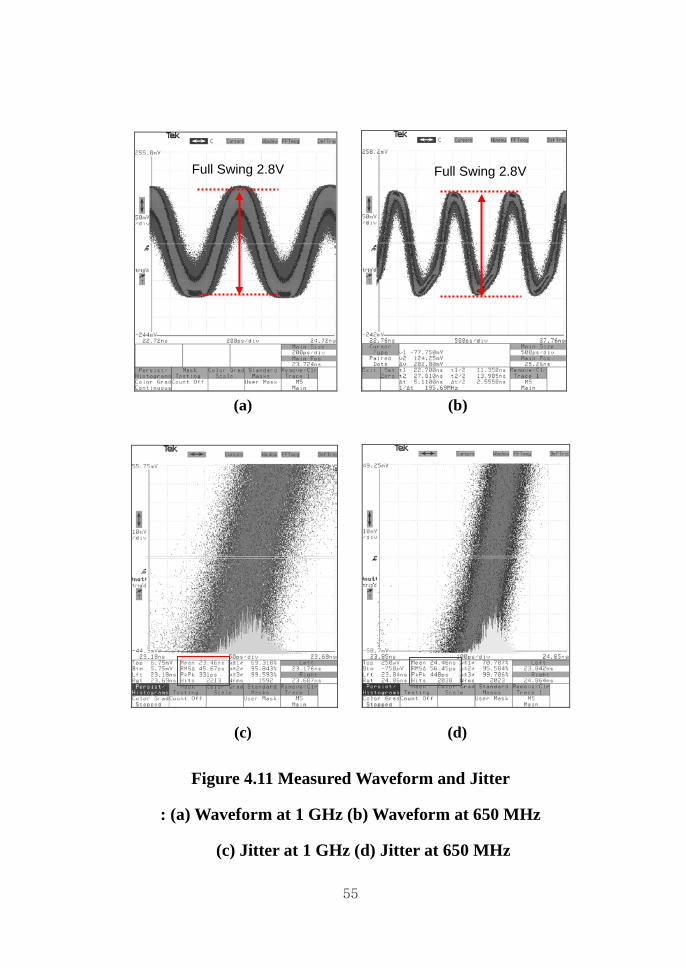
And figure 4.10 (a), (b) shows the PLL output clock by measuring
oscilloscope. The output clock is full swing at supply power 2.8 V. This
full swing voltage clock is used for MIPI interface block or SMIA
interface block sufficiently. Figure 4.10 (c), (d) shows the jitter of PLL
output clock. A rms jitter is measured 45.67 ps and a pk-pk jitter is 331
ps when the output clock is locked 1 GHz. When the output clock is
locked 650 MHz, a rms jitter is measured 56.45 ps and a pk-pk jitter is
448 ps, so the jitter characteristic is not good as 29 ~ 33 %.
55
(a) (b)
(c) (d)
Figure 4.11 Measured Waveform and Jitter
: (a) Waveform at 1 GHz (b) Waveform at 650 MHz
(c) Jitter at 1 GHz (d) Jitter at 650 MHz
Full Swing 2.8V Full Swing 2.8V
56
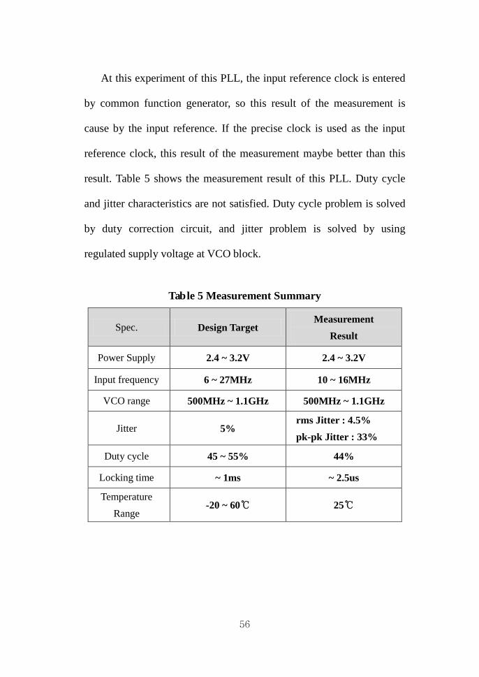
At this experiment of this PLL, the input reference clock is entered
by common function generator, so this result of the measurement is
cause by the input reference. If the precise clock is used as the input
reference clock, this result of the measurement maybe better than this
result. Table 5 shows the measurement result of this PLL. Duty cycle
and jitter characteristics are not satisfied. Duty cycle problem is solved
by duty correction circuit, and jitter problem is solved by using
regulated supply voltage at VCO block.
Table 5 Measurement Summary
Spec. Design Target Measurement
Result
Power Supply 2.4 ~ 3.2V 2.4 ~ 3.2V
Input frequency 6 ~ 27MHz 10 ~ 16MHz
VCO range 500MHz ~ 1.1GHz 500MHz ~ 1.1GHz
Jitter 5% rms Jitter : 4.5% pk-pk Jitter : 33%
Duty cycle 45 ~ 55% 44%
Locking time ~ 1ms ~ 2.5us
Temperature Range
-20 ~ 60℃ 25℃

57
CHAPTER Ⅴ
Conclusion
In this dissertation, a wide range PLL for MIPI and SMIA interface
at mobile image sensor is designed and fabricated 0.35um thick
transistors in 0.18um mixed CMOS technology.
The designed PLL uses 6 ~ 27MHz external reference clock and
generates 1GHz output clock for MIPI standard interface or 650MHz
output clock for SMIA standard interface. The output clock is 64
divided through dynamic logic divider to meet the input bandwidth. A
VCO is designed 4 stage ring type by PMOS latched delay cell and
operates well at PVT variation at the MIPI and SMIA standard
specifications. A frequency locking time is under 2.5us and power
consumption is 20mW, when this PLL operates at 1GHz, 2.8V power
supply. The core area occupies 121 × 51 um2
The measurement of the designed PLL is tested by measuring VCO
frequency range, locking frequency and jitter. VCO range is measured
500MHz ~ 1.1GHz at 2.4V ~ 3.2V power supply and phase noise is
76cBc/1MHz, and rms jitter is 4.5%, pk-pk jitter is about 30%. If the
jitter characteristic is improved well, this PLL can be adopted at high
.

58
resolution mobile CMOS image sensors for MIPI or SMIA interface.
The performance of this designed PLL is compared with other works at
table 6.
Table 6 Comparison with Performance of PLL
Item [5] [15] [16] This Work
Power Supply
2.4~ 2.9V 1.8V 3.3V 2.4 ~ 3.3V 2.8V(typ)
Locking Time
~ 30us ~ 10us ~ 3.5us ~ 2.5us
VCO Type Ring LC tank Ring Ring
VCO Tuning Range
32MHz ~ 440MHz
50MHz ~ 900MHz
300MHz ~ 1GHz
500MHz ~ 1.1GHz
VCO Gain 670MHz/V 94MHz/V 430MHz/V 810MHz/V
pk-pk Jitter 304ps 200ps 331ps
Duty Cycle 40 ~ 60% - - 44%
Phase Noise - 106dBc/100kHz - 76dBc/1MHz
Power Consumption
19mW 36mW 92mW 20mW
Technology 0.35um 0.18um 0.6um 0.35um

59
Bibliography
[1] J. H. Kim, J. C. Shin, C. R. Moon, S. H. Lee, D. C. Park, H. G.
Jeong, D. W. Kwon, J. W. Jung, H. P. Noh, K. B. Lee, K. G. Koh, D. H.
Lee and K. N. Kim, "1/2.5" 8 mega- pixel CMOS Image Sensor with
enhanced image quality for DSC application", IEDM, Dec 2006.
[2] www.mipi.org
[3] M. Y. Eom, J. G. Oh, and S. W. Kim, "Camera Interface Method in Mobile Handset and its Performance Comparison", ICPPW International Conference on, pp. 33-33, Sep 2007.
[4] www.smia-forum.org
[5] Y. W. Lee, “A Low Voltage and Wide Range Phase-Locked Loop for
Standard Mobile Imaging Architecture”, M.S dissertation, Graduate
school of engineering, Yonsei University, Dec 2005.
[6] B. Razavi, “Design of Analog CMOS Integrated Circuits”,
McGrawHill, 2001.
60
[7] P. K. Hanumolu, “Analysis of Charge-Pump Phase_Locked Loops”,
IEEE Transaction on circuits and systems, Vol. 51, pp. 1665-1674, Sep.
2004.
[8] Z. Shu, K. L. Lee, and B. H. Leung, "A 2.4-GHz Ring-Oscillator-
Based CMOS Frequency Synthesizer With a Fractional Divider Dual-
PLL Architecture" IEEE J. Solid-State Circuits, Vol. 39. No. 3, pp. 452-
462, Mar 2004.
[9] E. Gardner, “Charge-pump phase-lock loops”, IEEE Trans.
Commun, Vol. COM-28, pp. 1894-1858, Nov. 1980.
[10] E. H. M and F. Yuan, "An overview of low-voltage delay cells and
a worst-case analysis of supply noise sensitivity", Electrical and
Computer Engineering, 2004. Canadian Conference on,1785-1788 Vol.
3, May 2004
[11] J. S. Lee, "A low-noise fast-lock phase-locked loop with adaptive
bandwidth control ", IEEE Journal of Solid-State Circuit, vol.35. No. 8.
Aug. 2000.
61
[12] J. G. Maneatis and M. A. Horowitz, "Precise Delay Generation
Using Coupled Oscillators", IEEE Journal of Solid-State Circuit, vol.28.
No. 12. Dec 1993.
[13] J. U. Lee, “Research of Gbps Data an d Clock Recovery Circuit” ,
M.S dissertation, Graduate school of engineering, Yonsei University,
Jun 2001.
[14] Y. Ye, “Analysis and simulation three order charge-pump phase-
lock loop”, IEEE international conference on wireless communications,
networking and mobile computing, 12-14, Oct. 2008.
[15] S. O. Ko, “Design of a wide-band cmos frequency synthesizer for
DTV applications”, 2009 SOC conference, session A3.3. May 2009.
[16] H. J. Sung, “A 3.3V cmos dual-looped PLL with a current-
pumping algorithm”, IEICE trans. fundamentals, vol.E83-A. No. 2. Feb
2000.

62
국문요약
모바일 CMOS 이미지 센서용
MIPI와 SMIA 인터페이스 지원을 위한
광대역 위상 동기 루프 설계에 관한 연구
최근 모바일 이미지 센서는 CMOS 공정기술의 발전에 따
라 해상도가 높아지고 있으며 이에 따른 이미지 센서의 출력
을 위한 SMIA 인터페이스와 MIPI 인터페이스를 지원하도록
규정하고 있다. 본 연구에서는 이러한 고해상도 이미지 센서에
사용되는 고속 인터페이스를 지원하는 저전력 및 광대역 위상
동기 루프 설계에 관한 연구이다.
모바일 이미지 센서의 외부 클록인 6 ~ 27MHz의 기준 클록
을 사용하여 MIPI 인터페이스를 지원하기 위한 1GHz 및
SMIA 인터페이스를 지원하기 위한 650MHz의 출력 클록을 얻
기 위해 TSPC 타입의 분주기를 사용하여 64분주하도록 하였
고, 공정변화 및 전압과 온도에도 SMIA용 650MHz에서 MIPI
용 1GHz까지 동작하도록 PMOS Latched delay cell을 4단 연결한
63
RING 타입의 전압조절 발진기를 설계하였으며, 주파수 락킹
시간은 2.5us 이하 및 MIPI 인터페이스용 클록으로 1GHz로 락
킹되어 동작했을 경우 공급전압 2.8V에서 소비전력은 20mW로
설계하였다.
본 연구의 실측 검증을 위하여 0.18um CMOS 표준공정을
사용하여 설계하였으며, 특히 모바일 이미지 센서용으로서 대
기 누설 전류를 최소화 하기 위해 트랜지스터의 게이트 길이
가 0.35um인 Thick CMOS 트랜지스터를 사용하여 설계하였다.
설계된 위상 동기 루프의 측정 결과 주파수 범위는 공급전압
2.4V ~ 3.2V에서 500MHz ~ 1.1GHz의 발진 클록을 확보하였고,
1GHz 및 650MHz에서 Phase noise 측정 결과 76cBc/1MHz를 확
인할 수 있었다. 지터 특성은 1GHz로 동기되었을 때 45.67ps,
650MHz로 동기되었을 때 56.45ps로 측정되었다.

A Wide Range PLL Research
for MIPI and SMIA Interface
at Mobile CMOS Image Sensor Applications
Sun-Yong Park
The Graduate School
Yonsei University
Department of Electrical and Electronic Engineering
A Wide Range PLL Research
for MIPI and SMIA Interface
at Mobile CMOS Image Sensor Applications
Master’s Thesis
Submitted to the Department of Electrical and Electronic Engineering
and the Graduate School of Yonsei University
in partial fulfillment of the requirements
for the degree of Master of Science
Sun-Yong Park
December 2009

This certifies that the master’s thesis of Sun-Yong Park is approved.
___________________________
Thesis Supervisor: Woo-Young Choi
___________________________
Gun-Hee Han
___________________________
Seong-Ook Jung
The Graduate School
Yonsei University
December 2009

iii
Contents Figure Index_____________________________________________ iv
Table Index _____________________________________________viii
Abstract ________________________________________________ix
1. Introduction____________________________________________1
2. Motivation and Research Background ______________________4 2-1. Interface at Mobile Image Sensor_______________________4 2-2. MIPI Interface______________________________________8 2-3. SMIA Interface____________________________________11
2-4. PLL basic fundamentals_____________________________12
3. Design of PLL_________________________________________20 3-1. Proposed PLL system diagram________________________20 3-2. Design of a Phase Frequency Detector________________22 3-3. Design of a Charge Pump ___________________________26 3-4. Design of a Wide Range Voltage Controlled Oscillator_____29 3-5. Design of a Frequency Divider________________________35
3-6. Degisn of a Loop Filter _____________________________38
4. IC Fabrication and Experiment Results______________________45 4-1. IC Fabrication_____________________________________45
4-2. Experiment Results_________________________________47
5. Conclusion___________________________________________57
Bibliography_____________________________________________59 Abstract (in Korean) ______________________________________62

iv
Figure Index
Figure 1.1 Function Block Diagram of Image Sensor______________2
Figure 2.1 Parallel Interface Diagram of Image Sensor_____________5
Figure 2.2 Output Bandwidth Trend of Image Sensor______________6
Figure 2.3 Serial Interface Diagram of Image Sensor______________7
Figure 2.4 CSI-2 Layer and PHY Layer Definition________________8
Figure 2.5 Structure of Data Land Physical Layer in Image Sensor__10
Figure 2.6 Block Diagram of a PLL___________________________12
Figure 2.7 Simple Charge Pump PLL Structure__________________13
Figure 2.8 Step Response of PFD / CP / LPF ___________________14
Figure 2.9 Linear Model of Simple Charge Pump PLL____________15
Figure 2.10 2ND
Figure 2.11 3
Order Charge Pump PLL______________________16
RD
Figure 3.1 Proposed Structure of PLL System___________________21
Order Charge Pump PLL______________________18
Figure 3.2 Implementation of Phase Frequency Detector__________22

v
Figure 3.3 Phase Frequency Detector, (a) Logic level circuit, (b)
Layout_________________________________________________24
Figure 3.4 Waveform of Phase Frequency Detector______________24
Figure 3.5 Dead Zone of Phase Frequency Detector______________25
Figure 3.6 Reset Time at Frequency matched___________________25
Figure 3.7 Charge Pump and Loop Filter Circuits________________26
Figure 3.8 Simulation of Current Mismatch____________________27
Figure 3.9 Transient Simulation of PFD / CP___________________28
Figure 3.10 Unit Differential Delay Cell, (a) Circuit, (b) Layout____30
Figure 3.11 Waveform of Differential Unit Delay Cell____________31
Figure 3.12 Structure of 4 Stage Differential Ring Osicllator_______32
Figure 3.13 Layout of 4 Stage Differential Ring Osicllator_______32
Figure 3.14 Simulation Result of VCO range, (a) -20 ℃, (b) 60 ℃__33
Figure 3.15 64 Divider Structure_____________________________35
Figure 3.16 2 Divider Circuit and Operation Sequence ________36
Figure 3.17 Layout of 64 Divider____________________________36
vi
Figure 3.18 Simulation Waveform of 64 Divider_________________37
Figure 3.19 Linear Model of Charge Pump PLL with N divider_____38
Figure 3.20 Bode Plot of Designed PLL Transfer Function, (a) Open
Loop, (b) Closed Loop_____________________________________41
Figure 3.21 Transient Simulation of Locking Time_______________42
Figure 3.22 Damping Split Bode Plot of PLL Transfer Function, (a)
Open Loop, (b) Closed Loop________________________________43
Figure 3.23 Transient Simulation of Control Voltage at Damping Split ,
(a) 0 ~ 4 us, (b) 3.6 ~ 3.85 us________________________________44
Figure 4.1 Layout of PLL Chip______________________________46
Figure 4.2 Layout of PLL Core______________________________46
Figure 4.3 Evaluation Board for Fabricated Chip________________47
Figure 4.4 Block Diagram of Test Environment_________________48
Figure 4.5 Test Setup Picture, (a) Spectrum Analyzer, (b) Digital
Oscilloscope_____________________________________________49
Figure 4.6 Measured VCO Frequency Range___________________51
vii
Figure 4.7 Frequency Error Rate between Simulation and Measurement
_______________________________________________________51
Figure 4.8 Real Picture of Power Spectrum at Locked, (a) Span 200
MHz, (b)Span 1 MHz MIPI mode, (c) Span 1 MHz SMIA mode__52
Figure 4.9 Measured Power Spectrum of PLL, (a) for MIPI, (b) for
SMIA__________________________________________________53
Figure 4.10 Measured Phase Noise of Frequency Synthesizer______54
Figure 4.11 Measured Waveform and Jitter, (a) Waveform at 1 GHz, (b)
Waveform at 650 MHz, (c) Jitter at 1 GHz, (d) Jitter at 650
MHz___________________________________________________55
viii
Table Index
Table 1. PLL Specification for MIPI and SMIA standard__________11
Table 2. Simulation Result of VCO Range_____________________34
Table 3. Loop Filter Constants_______________________________40
Table 4. Measurement Result of VCO Frequency Range __________50
Table 5. Measurement Summary _____________________________56
Table 6. Comparison with Performance of PLL _________________58

ix
Abstract
A Wide Range PLL Research
for MIPI and SMIA Interface
at Mobile CMOS Image Sensor Applications
By
Sun-Yong Park
Department of Electrical and Electronic Engineering
The Graduate School
Yonsei University
Recently, a mobile image sensors has high resolution image
quality by developing CMOS process technology and the output
bandwidth of the image sensor has increased, so it is classified to
x
support the standard interface as MIPI (Mobile Industry Processor
Interface) standard or SMIA (Standard Mobile Imaging Architecture)
standard. This these is a research about a low power and wide range
frequency synthesizer to generate high speed timing clock for MIPI and
SMIA standard serial interface which is used at high resolution mobile
CMOS image sensors.
The designed frequency synthesizer uses 6 ~ 27 MHz external
reference clock and generates 1GHz output clock for MIPI standard
interface or 650MHz output clock for SMIA standard interface. The
output clock is 64 divided through TSPC (True single phase clock) type
divider to meet the bandwidth the output clock and the external
reference clock. A VCO (Voltage Controlled Oscillator) is designed 4
stage ring type by PMOS latched delay cell to operate well at process
variation, power supply and temperature variation to meet the MIPI and
SMIA standard specifications. This design is based on 0.18um CMOS
standard process, specially a 0.35 um thick gate oxide IO transistor is
used all circuit block to minimize the stand by current for mobile image
sensor. A frequency locking time is under 2.5 us and power
consumption is 20mW, when this frequency synthesizer operates at 1
GHz, 2.8 V power supply. The core area occupies 121 × 51 um2
The result of the designed frequency synthesizer is confirmed by
.
xi
measuring VCO frequency range, locking frequency and jitter. VCO
range is measured 500 MHz ~ 1.1 GHz at 2.4 V ~ 3.2 V power supply
and phase noise is 76 dBc/ 1 MHz. A RMS jitter is measured 45.67 ps
when the output clock is locked 1 GHz, 56.45 ps when the output clock
is locked 650 MHz.
Keywords: MIPI (Mobile Industry Processor Interface), SMIA
(Standard Mobile Imaging Architecture), Image Sensor,
PLL, Ring Oscillator, Latched Delay Cell, TSPC (True
Single Phase Clock) latched divider

1
Chapter Ⅰ
Introduction
1.1 Phase Locked Loop in Mobile CMOS image sensor
Lately, a mobile CMOS image sensor has been smaller and higher
resolution than before. Today, The minimum pixel size of 1.4 um ×
1.4 um is used at 5mega or 8mega mobile image sensor. A few years
ago, the past mobile image sensor had low resolution as 70 k ~ 1.3 M
pixels and there has parallel interface to transfer the output pixel data.
The output digital 10 bit or 12 bit data are sent to the receiver backend
chip through parallel interface. At the high resolution image sensor, the
output bandwidth is increased rapidly to send the amount of the 5mera
or 8mega pixel data. So, MIPI or SMIA serial interface is adapted at
commercial image sensor product and a frequency synthesizer in the
image sensor has to generate a 1 GHz clock for MIPI interface or a 650
MHz clock for SMIA interface.
Generally, 6 ~ 27 MHz external reference clock from a mobile set
board entered to a mobile image sensor and a phase locked loop in a
mobile image sensor generates internal clock for driving pixel arrays
and serializing the pixel output data.

2
Figure 1.1 Function Block Diagram of Image Sensor
Figure 1.1 illustrates the function block diagram of image sensor.
It is consists of 6 blocks largely, Active pixel array which is occupied
almost of the chip area is generate the pixel analog data from the photo
diode. CDS circuits are sampling the pixel signal level and reset level
by Correlate Double Sampling method. ADC circuits change the
sampled analog pixel signal to digital code. Row decoder drives APS
array selectively by progressive method. Timing generator block
control the clock signal to operate the row decoder, CDS circuits, ADC
circuits. And frequency synthesizer generates the system clock using
the external reference clock.
This dissertation will focus on the research of interface method in

3
image sensors and the design and implementation of a frequency
synthesizer to meet the MIPI and SMIA interface standard in the high
resolution image sensors. At first, backgrounds of the interface of
image sensors will be explained, and then the basic operation of the
PLL and the loop dynamics will be described. Details of this
dissertation outline are as follows.
In chapter Ⅱ, Motivation and research background is discussed.
Section 2.1 introduces a interface of a image sensor. In section 2.2, the
MIPI interface standard will be shown in section 2.3 the SMIA
interface standard will be shown. And in section 2.4 describes the basic
of PLL and the loop dynamics.
Next, in chapter Ⅲ, the PLL design is described. At first, proposed
PLL is introduced in section 3.1. The designs of a phase frequency
detector, a charge pump circuits, a voltage controlled oscillator and
frequency divider are described in section 3.2 ~ 3.5. The design of a
loop filter is shown in section 3.6.
In chapter Ⅳ, IC fabrication and measurement are discussed. In
section 4.1, IC fabrication by 0.18um CMOS process is described, and
measurement results of fabricated chip are discussed in section 4.2.
At last, chapter Ⅴ summarizes results of the wide range PLL for
MIPI and SMIA interface at a mobile image sensor.

4
Chapter 2
Motivation and Research Background
2.1 The Interface of a Mobile Image Sensor
The pixel output data which are generated by the image sensor are
sent to the host backend chip for display or storage. First of all, the
output bandwidth (or the amount of the pixel output data) is calculated
below equation.
Output Bandwidth = Number of Horizontal pixels (include
Horizontal blank data) × Number of vertical pixels (include vertical
blank data) × 8bit ~ 12bit binary data of unit pixel × Number of
Frames/sec (2.1)
There are two types of the interfaces between mobile CMOS image
sensor and host for transmission of the pixel output data. One is
common parallel mode interface and the other is a serial mode interface.
A few years ago, we had used the mobile cellular phone which had
a camera and the resolution of that had 0.3mega pixels as VGA image
format. Also the pixel size of that image sensor is 3.5um × 3.5um.

5
The image data of the VGA camera system has about 100Mega
pixels binary data from the equation (2.1) that is operating at
15frames/sec, so the image data transmission is capable well at the
parallel mode interface.
Figure 2.1 Parallel Interface Diagram of Image Sensor
Figure 2.1 shows the parallel mode interface diagram at image
sensor. The parallel mode interface need 8 ~ 12bits data output, vertical
sync signal output, horizontal sync signal output and pixel clock. When
the image sensor send the YUV image format, the output data is used
8bit outputs normally and when the image sensor send the Bayer image
format(or pixel raw data) data is used 10 ~ 12bit outputs.
Recently, the pixel technology of a CMOS image sensor has
developed rapidly as figure 2.2 that show the output bandwidth trend of
6
the image sensor.
Figure 2.2 Output Bandwidth Trend of Image Sensor
The unit pixel size has reached 1.7um X 1.7um and the resolution
has increased to 5mega (QSXGA image format) ~ 8mega (QUXGA
image format) pixels. For example, at 8 mega pixels (column 3360
pixels× row 2550 pixels) QUXGA camera system[1], the output data
have about 1.4giga pixels binary data when the image sensor is
operating at 15frames/sec. At this high resolution camera system,
common parallel mode interfaces are difficult to expand and consume
very large amounts of power because the voltage swing range of a
parallel interface is 1.8 ~ 2.8V.
But the serial mode interface uses LVDS differential signal and
their voltage swing range is 150mV ~ 200mV to transfer pixel data, so
7
the advantage of the serial mode interface is low power consumption,
high speed data transmission, scalable and cost effective because the
number of Input / Output pin is reduced. And the disadvantage of the
serial interface needs the extra function block for the packet data
transformation of the pixel output data. Lately, the commercial
standards of the serial mode interface are SMIA and MIPI standard at
mobile CMOS image sensor. Figure 2.3 illustrates the serial interface
diagram of image sensor.
Figure 2.3 Serial Interface Diagram of Image Sensor
The two kinds of serial interface standards will be shown more
detail at the next chapter.

8
2.2 MIPI Introduction
The MIPI interface is largely consist of the CSI-2(Camera Serial
Inteface-2) protocol layer and the physical layer as illustrated in Figure
2.4.
Figure 2.4 CSI-2 Layer and PHY Layer Definition
At first, in the pixel to byte packing formats layer, the output pixel
binary data (YUV, BGR, Bayer format) from the image sensor is
packed to bytes format before sending the data to the low level protocol

9
layer. Also in the receiver (or host backend chip), this layer unpacks
bytes from the low level protocol layer into the original pixel data.
At the low level protocol layer, the received bytes data change
packet data form for serial data transmission. At the lane management
layer, the received packet data is distributed multi lane. This CSI-2
protocol is allowable the extension of the lane, so the lane may be one,
two, three or four depending on the output bandwidth requirements of
the application and the maximum bandwidth of the one lane is 1Gbps.
For example, in case of the 8mega image sensor, the output bandwidth
is needed about 1.4Gbps, so it is impossible to transfer the packet data
through only one lane. It may use the two lanes for the transmission of
the high resolution image packet data. Also in the receiver, this layer
recombines the each lane data stream.
At the physical layer, the separated packet data transfer the serial bit
stream through the LVDS (Low Voltage Differential Signal) form. In
LVDS mode, 0.2V common mode voltage at HS (High speed) mode,
1V common mode voltage at LP (Low Power), and their voltage swing
range is 0.2V.
Figure 2.5 shows the structure of data lane physical layer. It is
consist of the two data lanes driver and one clock lane driver. In master

10
IC or image sensor, PLL drives image sensor timing generator and
MIPI physical clock and data lane using external clock. And MIPI
clock and data lane transmitter send the LVDS signal. Slave IC or
image signal processor chip is getting the LVDS signal through MIPI
receiver [2], [3].
Figure 2.5 Structure of Data Lane Physical Layer in Image Sensor
11
2.3 SMIA Introduction
SMIA means Standard Mobile Imaging Architecture and it is
classified the standard specification of the mobile image camera
module announced by Nokia and ST Microelectronics at July 2004. At
the interface system of the SMIA specification, there are consist of the
IIC control interface and the LVDS data transfer interface. The
maximum output bandwidth is 650Mbps and the LVDS common mode
voltage is 1V [4]. But this limited output bandwidth is not acceptable in
the high resolution image sensor as 5mera or 8mega pixels.
Table 1 shows the PLL specification for MIPI and SMIA standard
and the designed PLL has to meet this specification.
Table 1 PLL Specification for MIPI and SMIA Standard [5]
Spec. MIPI
specification SMIA
specification
Power Supply 2.4 ~ 3.2V
Input frequency 6 ~ 27MHz
Output frequency ~ 1GHz ~ 650 MHz
Jitter No spec 5%
Duty cycle 40 ~ 60% 45 ~ 55%
Locking time ~ 1ms
Temperature Range -20 ~ 60℃

12
2.4 PLL Basic Fundamentals
Figure 2.6 illustrates the block diagram of a PLL system. A PLL is a
closed loop feedback system that makes fixed phase between its output
clock phase of oscillator and a reference clock phase.
The basic operation of a PLL is as follows. The phase detector
compares the phase of the feedback oscillator clock and the phase of
the output reference clock, and makes an error output signal. The
difference of phase or error signal is low pass filtered by charge pump
block and Loop filter block. This filtered error signal drive a voltage
controlled oscillator as a control signal to adjust the frequency of the
oscillator. The frequency of oscillation is divided down to match the
same bandwidth of the reference clock by a frequency divider.
The PLL is locked when the feedback clock is the same frequency
as the reference clock.
Figure 2.6 Block Diagram of a PLL

13
2.4.1 Loop Dynamics in Charge Pump PLL
This section describes the dynamics of the Phase Locked Loop.
Figure 2.7 is called a charge pump PLL structure. The phase frequency
detector block is consist of two edge-triggered resettable D flip flops
with their D inputs tied to a logical one and the block detects the phase
or frequency differences and drives the charge pump accordingly. When
the ωout is far from ωin, the PFD and the charge pump change the
control voltage to approach ωin, also the input and output frequencies
are close, the PFD operates as a phase detector, so locks the phase.
Figure 2.7 Simple Charge Pump PLL Structure
In order to analysis the dynamic characteristic of the charge pump
PLL system, the components are created as a linear model to make the
transfer function [6].
14
Figure 2.8 Step Response of PFD / CP / LPF
As illustrated in Figure 2.8 at the input period Tin, the charge pump
generates a current of ± IP to the capacitor CP. The slope of Vcout
02P
P
ISlopeC
φπ
=
is
(2.2)
So, the Vcout
0( ) ( )2
Pout
P
IV t t u tC
φπ
=
can be expressed as
(2.3)
And the impulse response is given by
( ) ( )2
P
P
Ih t u tCπ
= (2.4)
Then the transfer function is
1( )2
out P
P
V IsC sφ π
=∆
(2.5)

15
Also, the gain of phase frequency detector, KPFD
2P
PFDIKπ
=
is
(2.6)
2.4.2 Dynamics at Simple Charge Pump PLL
Figure 2.9 Linear Model of Simple Charge Pump PLL
Figure 2.9 shows the linear model of simple charge pump PLL. At
this model, when we use the single capacitor CP
1 1( )P
F sC s
=
as Figure 2.7, loop
filter transfer function F(s) is
(2.7)
Hence the open loop transfer function as
2( ) ( )2
out vcoPopen
in Popen
KIs H sC sπ
Φ= =
Φ (2.8)
16
And the closed loop transfer function as
2
22
( ) 2 2( )1 ( ) 1
2 2
VCO P VCOP
open P Pclosed
VCO P VCOPopen
P P
K I KIH s C s CH s K I KIH s s
C s C
π π
π π
= = =+ + +
(2.9)
But this closed loop system is unstable, because it contains two
imaginary poles [6].
2.4.3 Dynamics at 2ND
In order to improve the above charge pump PLL system, a resistor
R
Order Charge Pump PLL
P is introduced in series with the loop filter capacitor to generate a
stabilizing zero to improve the phase margin in the loop gain at Figure
2.10.
Figure 2.10 2ND
Order Charge Pump PLL

17
And the modified loop filter transfer function as
1( ) ( )PP
F s RC s
= + (2.10)
Hence the open loop transfer function as
1( ) ( ) ( )2
out vcoPopen P
in Popen
KIs H s RC s sπ
Φ= = +
Φ (2.11)
And the closed loop transfer function as
1( )( ) 2( )11 ( ) 1 ( )
2
vcoPP
open Pclosed
vcoPopenP
P
KI RH s C s sH s KIH s RC s s
π
π
+= =
+ + +
2
( 1)2
2 2
P VCOP P
P
P VCO P VCOP
P
I K R C sC
I K I Ks R sC
π
π π
+=
+ + (2.12)
At this 2ND order charge pump PLL system, the charge pump drives
the series resistor RP and capacitor CP
, so a current is injected into the
loop filter at each period time. This cause the large jumping voltage to
the control voltage and even in the locked condition, the mismatches
between charge current and discharge current of the charge pump and
the clock feed-through of the charge pump switches cause the jumping
voltage also. This ripple modulates the frequency of the voltage
controlled oscillator and introduces excessive jitter [6].

18
2.4.4 Dynamics at 3RD
In order to improve the 2
Order Charge Pump PLL
ND order charge pump PLL system, a small
capacitor is added in parallel with resistor RP and capacitor CP
loop
filter network as shown in Figure 2.11 to suppress the ripple induced
jitter in the output voltage.
Figure 2.11 3RD
But this capacitor C
Order Charge Pump PLL
S
The modified loop filter transfer function as
generates a pole, so increasing the order of the
charge pump PLL system to three and the phase degradation due to this
pole.
1
( ) 1( )P P
SP P S
sR CF s
C s sR C C
+=
+
(2.13)

19
Hence the open loop transfer function as
1
( ) ( ) 12 ( )out vcoP P P
openin open S
P P S
sKI R Cs H s
sC s sR C C
π
+Φ
= =Φ +
(2.14)
And the closed loop transfer function as
1
12 ( )( )( ) 11 ( )
1 12 ( )
vcoP P P
Sopen P P S
closedopen
vcoP P P
SP P S
sKI R C
sC s sH s R C CH sH s s
KI R CsC s s
R C C
π
π
+
+= =
+ ++
+
3 2
1( )2
1( )2 2
P VCO
S P P
P VCO P VCO
P P S S P P S
I K sC R C
I K I Ks s sR C C C R C C
π
π π
+=
+ + +
(2.15)
Here, if capacitor CS is about one-fifth to one-tenth of CP, the close
loop time and frequency responses of this 3RD order charge pump PLL
system are relatively unchanged with the 2ND order charge pump PLL
system [6], [7].
20
CHAPTER 3
Design of PLL
3.1 Proposed PLL System Diagram
Recently, the fabrication of standard CMOS process technologies
has been developed rapidly, and gate length reach to 32nm. But this fast
CMOS transistor is not acceptable to use mobile image sensors,
because of the leakage issue of transistor. For low operating power
consumption and minimization of stand-by power consumption, mobile
image sensors are designed by thick gate oxide transistor for analog
circuits and pixels except digital logic circuits which are used thin gate
oxide transistor. And analog power supply is used 2.8V for reduction of
operating power consumption. So, proposed PLL is designed by thick
gate oxide transistor for all circuit blocks and used 2.8V as power
supply voltage.
Figure 3.1 shows that designed PLL system overall diagram. The
phase frequency detector make up and down error pulses based on the
phase and frequency difference between the input reference clock and
divided feedback clock. The up and down error pulses drive charge
pumping switches to charge or discharge of loop filter components.
And the output voltage of loop filter controls the frequency of the

21
voltage controlled oscillator. Input reference clock is 6 ~ 27MHz and
voltage controlled oscillator output clock is about 1GHz, so frequency
divider divides 64 to meet the input reference clock bandwidth. The
system clock for MIPI interface and timing generator is generated by
output buffer.
Figure 3.1 Proposed Structure of PLL System

22
3.2 The Design of a Phase Frequency Detector
A general system for PLL uses a phase frequency detector for
acquisition of simultaneous phase and frequency between external
clock and internal generated clock. Figure 3.2 describes a common
linear phase frequency detector architecture using two edge-triggered
and resettable D-flip flops with their D inputs tied to a high state. This
phase frequency detector generates an up signal that switches to make
charge current of a charge pump and down signal that switches to make
discharge current of a charge pump [6], [8].
The D-flip flops are triggered by the external clock and the internal
clock. At the initial state, up and down output signals are low state.
When one of the external clock and the internal clock is rises, the
corresponding output rise high through the FSM state diagram.
Figure 3.2 Implementation of Phase Frequency Detector

23
Figure 3.3 illustrates the overall phase frequency detector at the
gate level and layout. It consists of X9 NOR gates and the X8 NOR
gate is reset by the output pulse of X0 and X1 NOR gate.
(a) (b)
Figure 3.3 Phase Frequency Detector
: (a) Logic level circuit (b) Layout
The phase freqeuncy detector was confirmed by the transient
simulation at the condition of 100MHz external clock and 101MHz
internal clock, and the figure 3.4 is shown the waveform of the up pulse
and down pulse. When the external frequency and the internal
frequency are matched, the up and down pulse rise high and reset to ‘0’
state as Figure 3.6. This reset time is 540ps to reject the deadzone that
phase freqeuncy detector may not generate enough time of the up/down
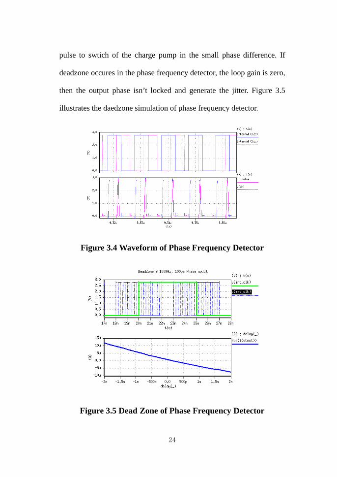
24
pulse to swtich of the charge pump in the small phase difference. If
deadzone occures in the phase frequency detector, the loop gain is zero,
then the output phase isn’t locked and generate the jitter. Figure 3.5
illustrates the daedzone simulation of phase frequency detector.
Figure 3.4 Waveform of Phase Frequency Detector
Figure 3.5 Dead Zone of Phase Frequency Detector

25
Figure 3.6 Reset Time at Frequency Matched

26
3.3 The Design of a Charge Pump
A charge pump block generates the current to drive the control
voltage of the voltage controlled oscillator. When the up pulse is
generated from the phase frequency detector, the current charges the
loop filter and when the down pulse is generated from the phase
frequency detector, the current discharges the loop filter. At this point,
the mismatch of the charge current and the discharge current and each
leakage current cause the static phase error when the PLL system is
locked. This periodical charge pump operation for compensation of this
error makes the high frequency harmonics at the control voltage, and it
generates a jitter [9].
To reduce the mismatch current, the charge pump circuit is used the
feedback amplifier as Figure 3.7.
Figure 3.7 Charge pump and Loop Filter Circuits

27
At this charge pump circuit, the transistors size of the left current
path is the same as the right current path and the voltage of the ‘ref’
node is the same voltage as the ‘vf’ node through the feedback
operation of the amplifier. Figure 3.8 show the current mismatch of this
charge pump circuit. When the up and down pulse enter the charge
pump circuit, ‘vf’ node is sweeped voltage from gnd to vdd to measure
the charge current and the discharge current. From the simulation result,
charge pump current ‘IP’ is 58 ~ 65uA at 2.8V power supply voltage
and this range is used to drive the control voltage. And mismatch
current is 2.1uA at 0.5V control voltage, 99nA at 2V control voltage.
Figure 3.8 Simulation of Current Mismatch
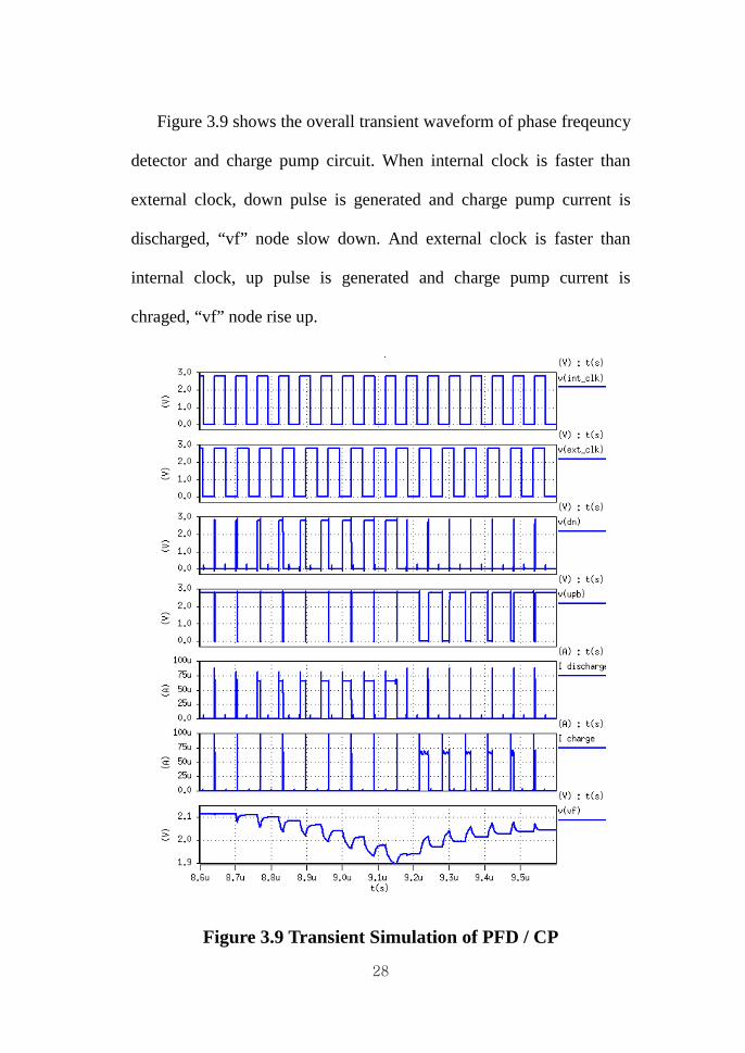
28
Figure 3.9 shows the overall transient waveform of phase freqeuncy
detector and charge pump circuit. When internal clock is faster than
external clock, down pulse is generated and charge pump current is
discharged, “vf” node slow down. And external clock is faster than
internal clock, up pulse is generated and charge pump current is
chraged, “vf” node rise up.
Figure 3.9 Transient Simulation of PFD / CP
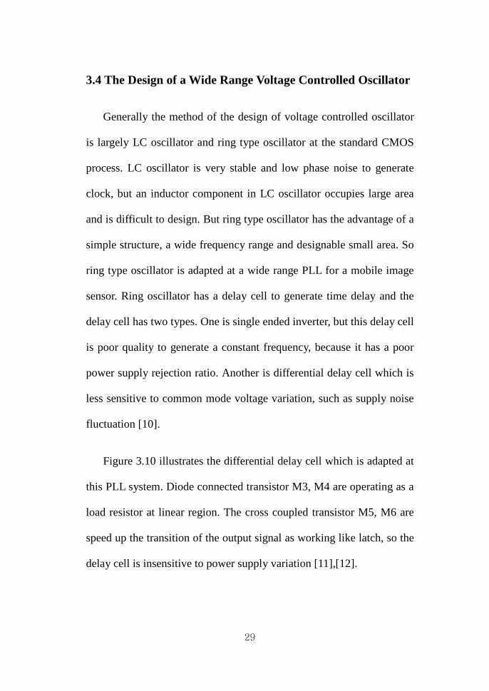
29
3.4 The Design of a Wide Range Voltage Controlled Oscillator
Generally the method of the design of voltage controlled oscillator
is largely LC oscillator and ring type oscillator at the standard CMOS
process. LC oscillator is very stable and low phase noise to generate
clock, but an inductor component in LC oscillator occupies large area
and is difficult to design. But ring type oscillator has the advantage of a
simple structure, a wide frequency range and designable small area. So
ring type oscillator is adapted at a wide range PLL for a mobile image
sensor. Ring oscillator has a delay cell to generate time delay and the
delay cell has two types. One is single ended inverter, but this delay cell
is poor quality to generate a constant frequency, because it has a poor
power supply rejection ratio. Another is differential delay cell which is
less sensitive to common mode voltage variation, such as supply noise
fluctuation [10].
Figure 3.10 illustrates the differential delay cell which is adapted at
this PLL system. Diode connected transistor M3, M4 are operating as a
load resistor at linear region. The cross coupled transistor M5, M6 are
speed up the transition of the output signal as working like latch, so the
delay cell is insensitive to power supply variation [11],[12].
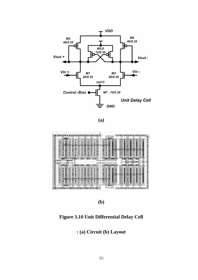
30
(a)
(b)
Figure 3.10 Unit Differential Delay Cell
: (a) Circuit (b) Layout

31
Figure 3.11 shows the waveform of the unit differential delay cell.
The “Vout” and “Voutb” nodes oscillate and the swing range is 1.3V ~
2.6V. The reason is as follows. If the diode connected PMOS resistor is
considered as equivalent “R”, and the tail current of the transistor M7 is
“IM7”, the output voltage swing range is about VDD ~VDD – R×IM7
And the “net13” node oscillates two times of the oscillation
frequency. [6]
.
Figure 3.11 Waveform of Differential Unit Delay Cell
Using this differential unit delay cell, 4tage ring oscillator is
designed for wide range oscillation shown as Figure 3.12. This even
stage oscillator have to connect cross coupled the output of the last
stage and the input of the first stage. If a level “0” and level “l” are
entered the first stage, the output of the last stage are a level “1” and

32
“0”, so the first stage is inverted after some delay time. And the period
of the N stage differential ring oscillator is 2NTDELAY. And figure 3.13
shows the layout of this 4 stage differential ring oscillator [6].
Figure 3.12 Structure of 4 Stage Differential Ring Oscillator
Figure 3.13 Layout of 4 Stage Differential Ring Oscillator
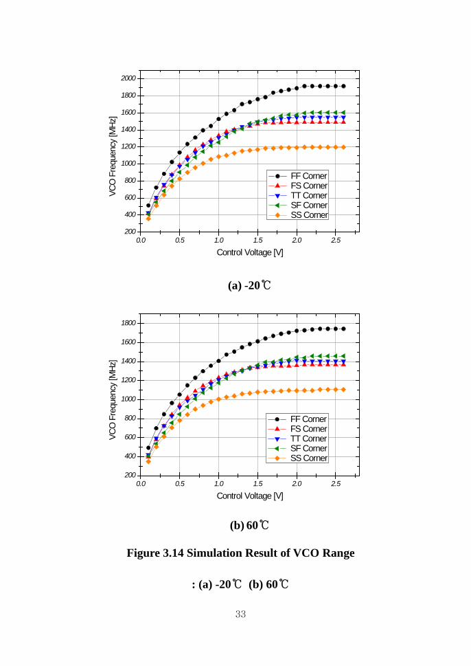
33
0.0 0.5 1.0 1.5 2.0 2.5200
400
600
800
1000
1200
1400
1600
1800
2000
VCO
Fre
quen
cy [M
Hz]
Control Voltage [V]
FF Corner FS Corner TT Corner SF Corner SS Corner
(a) -20℃
0.0 0.5 1.0 1.5 2.0 2.5200
400
600
800
1000
1200
1400
1600
1800
VCO
Fre
quen
cy [M
Hz]
Control Voltage [V]
FF Corner FS Corner TT Corner SF Corner SS Corner
(b) 60℃
Figure 3.14 Simulation Result of VCO Range
: (a) -20℃ (b) 60℃

34
Figure 3.14 shows the VCO range and it was simulated at PVT
variation to confirm the MIPI and SMIA standard specifications. The
designed 4 stage differential ring oscillator is operating well, the
maximum frequency at a low control voltage is 500MHz in 60℃, fast-
fast corner. And the minimum frequency at a high control voltage is
1.1GHz in 60℃, slow-slow corner. So the frequency range of this VCO
is 500MHz ~ 1.1GHz in PVT variation.
The simulation result of the VCO range is summarized at table 2.
Table 2 Simulation Result of VCO range
Transistor Corner (NMOS, PMOS)
Temperature
-20℃ 60℃
Fast-Fast Corner 450 MHz ~ 1.90 GHz 500 MHz ~ 1.70 GHz
Fast-Slow Corner 400 MHz ~ 1.50 GHz 400 MHz ~ 1.35 GHz
Typical Corner 400 MHz ~ 1.55 GHz 400 MHz ~ 1.40 GHz
Slow-Fast Corner 400 MHz ~ 1.60 GHz 400 MHz ~ 1.45 GHz
Slow-Slow Corner 350 MHz ~ 1.20 GHz 350 MHz ~ 1.10 GHz
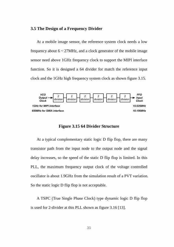
35
3.5 The Design of a Frequency Divider
At a mobile image sensor, the reference system clock needs a low
frequency about 6 ~ 27MHz, and a clock generator of the mobile image
sensor need above 1GHz frequency clock to support the MIPI interface
function. So it is designed a 64 divider for match the reference input
clock and the 1GHz high frequency system clock as shown figure 3.15.
Figure 3.15 64 Divider Structure
At a typical complementary static logic D flip flop, there are many
transistor path from the input node to the output node and the signal
delay increases, so the speed of the static D flip flop is limited. In this
PLL, the maximum frequency output clock of the voltage controlled
oscillator is about 1.9GHz from the simulation result of a PVT variation.
So the static logic D flip flop is not acceptable.
A TSPC (True Single Phase Clock) type dynamic logic D flip flop
is used for 2-divider at this PLL shown as figure 3.16 [13].
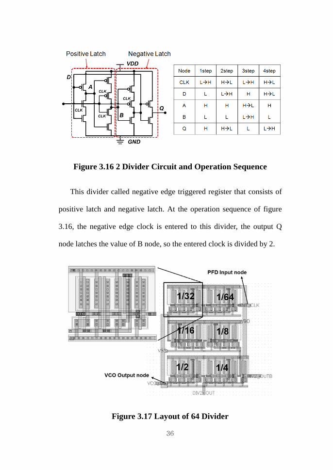
36
Figure 3.16 2 Divider Circuit and Operation Sequence
This divider called negative edge triggered register that consists of
positive latch and negative latch. At the operation sequence of figure
3.16, the negative edge clock is entered to this divider, the output Q
node latches the value of B node, so the entered clock is divided by 2.
Figure 3.17 Layout of 64 Divider

37
Figure 3.17 shows the layout of the 64-divider, and figure 3.18
shows the simulation result of the frequency at each divider output
node and the simulation waveform of the 64-divider. When the VCO
output frequency is 1GHz, the output frequency of the 64 divider is
15.625MHz.
Figure 3.18 Simulation Waveform of 64 Divider

38
3.6 The Design of a Loop Filter
The design of a loop filter is important as the stability and the
locking quality of a PLL system [9]. To stabilize the PLL system, it is
used a conventional 3rd
Figure 3.19 shows the linear model of a charge pump PLL with N
divider.
order loop filter. First of all, to achieve the
optimal value of a loop filter components register and capacitor, it is
calculated by the next equation.
Figure 3.19 Linear Model of Charge Pump PLL with N
divider
At this charge pump PLL with N divider, the closed loop transfer
function is modified from the equation (2.11) with N. So the closed
loop transfer function is

39
1( )( ) 2( ) 1 11 ( ) 1 ( )2
π
π
+= =
+ + +
vcoPP
open Pclosed
vcoPopen P
P
KI RH s C s sH s KIH s RN N C s s
(3.1)
And this equation can be the next form through the control theory.
2
2 2
22ζω ωζω ω
+=
+ +n n
n n
ss s
(3.2)
Hence, the Capacitor Cp and the register RP
22π ω=
vcoPP
n
KICN
is
(3.3)
4πζω= n
PP VCO
RI K
(3.4)
10= P
NCC (3.5)
Where IP is a charge pump current, N is a dividing factor, KVCO is a
VCO gain and each value is used by the simulation result shown as
Table 3. And the natural frequency (or the loop bandwidth) ωN should
be smaller than 1/10 of the reference frequency for the system stability.
In this work, input reference frequency is 15.6 MHz for MIPI interface,
and 10.15 MHz for SMIA interface, so the loop bandwidth ωN value is
selected about 8M rad/sec. The damping ratio ζ is 1 to get a fast
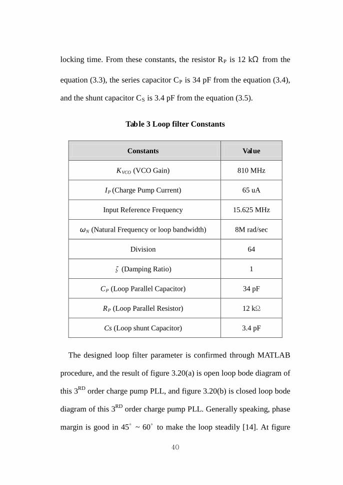
40
locking time. From these constants, the resistor RP is 12 kΩ from the
equation (3.3), the series capacitor CP is 34 pF from the equation (3.4),
and the shunt capacitor CS
Table 3 Loop filter Constants
is 3.4 pF from the equation (3.5).
Constants Value
KVCO (VCO Gain) 810 MHz
IP (Charge Pump Current) 65 uA
Input Reference Frequency 15.625 MHz
ωN (Natural Frequency or loop bandwidth) 8M rad/sec
Division 64
ζ (Damping Ratio) 1
CP (Loop Parallel Capacitor) 34 pF
RP (Loop Parallel Resistor) 12 kΩ
Cs (Loop shunt Capacitor) 3.4 pF
The designed loop filter parameter is confirmed through MATLAB
procedure, and the result of figure 3.20(a) is open loop bode diagram of
this 3RD order charge pump PLL, and figure 3.20(b) is closed loop bode
diagram of this 3RD order charge pump PLL. Generally speaking, phase
margin is good in 45˚ ~ 60˚ to make the loop steadily [14]. At figure
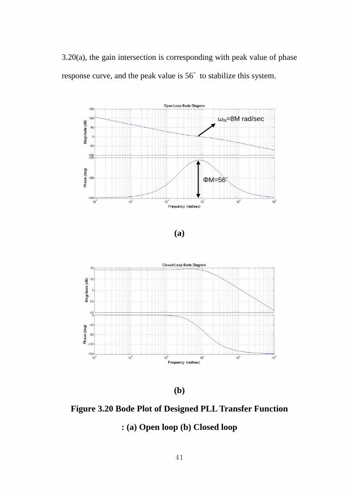
41
3.20(a), the gain intersection is corresponding with peak value of phase
response curve, and the peak value is 56˚ to stabilize this system.
(a)
(b)
Figure 3.20 Bode Plot of Designed PLL Transfer Function
: (a) Open loop (b) Closed loop
ΦM=56˚
ωN=8M rad/sec

42
Finally transient simulation was carried out over all PLL block with
the selected loop parameter as shown figure 3.21. 1 GHz clock PLL
output was locked about 1.5 us for MIPI clock at 0.627 V control
voltage and 650 MHz clock PLL output was locked about 2.5 us for
SMIA clock at 0.25 V control voltage.
Figure 3.21 Transient Simulation of Locking Time
If a damping ratio control the locking time and stability in the PLL
system. Figure 3.22 illustrates the bode plot of damping ratio splits
through MATLAB. When the damping ratio rises, the loop bandwidth

43
is reduced in the open loop transfer function, and magnitude rises in the
closed loop transfer function.
(a)
(b)
Figure 3.22 Damping Split Bode Plot of PLL Transfer
Function : (a) Open loop (b) Closed loop

44
At figure 3.23, when the damping ratio is over “1”, the PLL system
is unstable. But, when the damping ratio is “0.707” or “1”, the PLL
system is locked stable. The locking time of the damping ratio “1” is
faster than that of “0.707”.
(a)
(b)
Figure 3.23 Transient Simulation of Control Voltage at Damping Split : (a) 0 ~ 4us (b) 3.6 ~ 3.85us
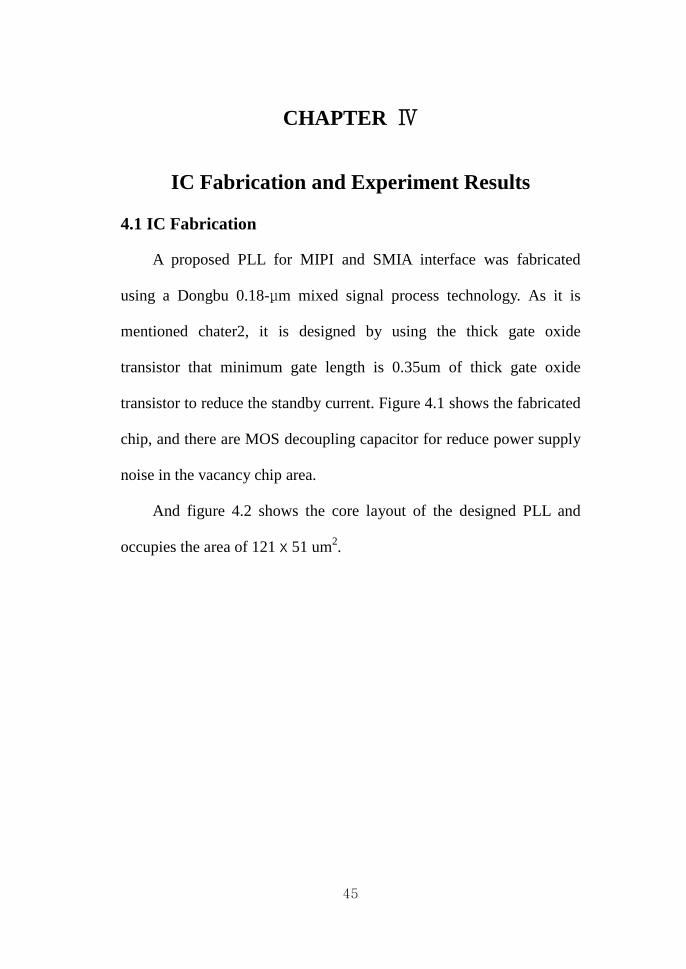
45
CHAPTER Ⅳ
IC Fabrication and Experiment Results
4.1 IC Fabrication
A proposed PLL for MIPI and SMIA interface was fabricated
using a Dongbu 0.18-μm mixed signal process technology. As it is
mentioned chater2, it is designed by using the thick gate oxide
transistor that minimum gate length is 0.35um of thick gate oxide
transistor to reduce the standby current. Figure 4.1 shows the fabricated
chip, and there are MOS decoupling capacitor for reduce power supply
noise in the vacancy chip area.
And figure 4.2 shows the core layout of the designed PLL and
occupies the area of 121 x 51 um2
.
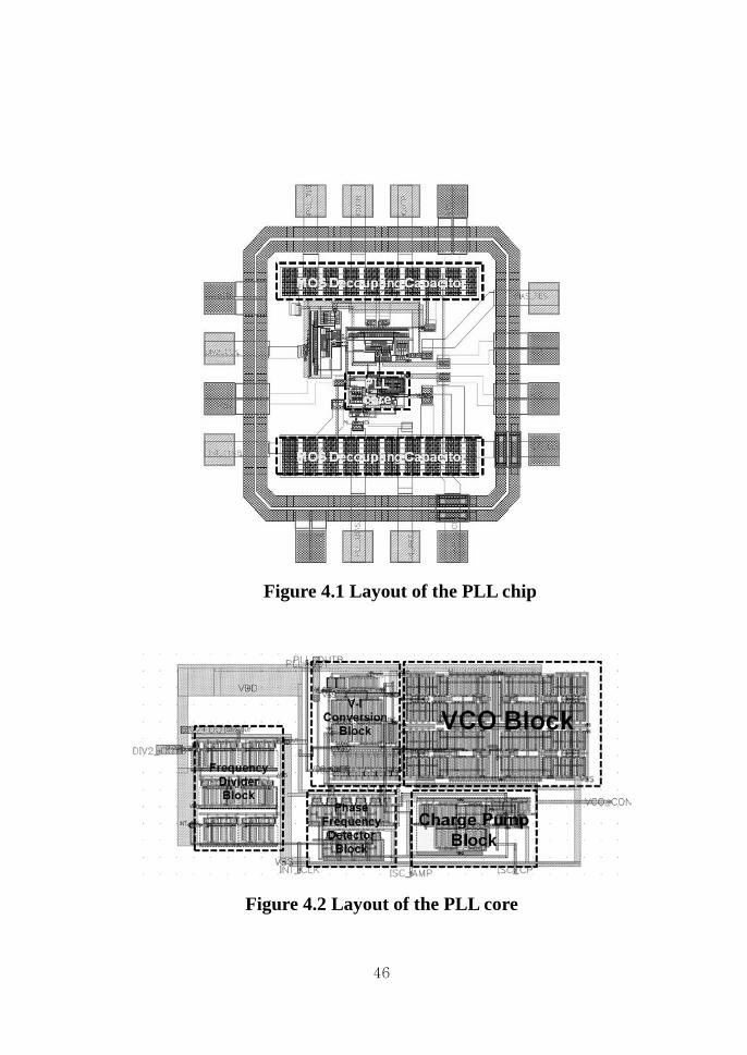
46
Figure 4.1 Layout of the PLL chip
Figure 4.2 Layout of the PLL core

47
4.2 Experiment Results
4.2.1 Printed Circuit Board Design
Figure 4.3 shows the evaluation board for fabricated chip. At the
printed circuit board, selector switch is used when the fabricated chip is
measured for evaluation of the PLL function or the VCO frequency
range. And the variable resistor controls the VCO control voltage for
measurement of the VCO frequency range when the evaluation board is
VCO measurement mode.
Figure 4.3 Evaluation Boards for Fabricated Chip
Variable Resistor
Power Supply
Selector Switch
Loop Filter
Fabricated Chip
Reference Clock Input
VCO Clock Output

48
4.2.2 Test Setup
Figure 4.4 illustrates the block diagram of the test environment. A
2.8V power is used by a single power supply and function generator is
connected the input clock to supply the input reference clock. The
digital oscilloscope is connected the output clock to confirm the
waveform and jitter. And spectrum analyzer is connected the output
clock to measure frequency and phase noise.
Figure 4.4 Block Diagram of Test Environment
Figure 4.5 shows the real picture when the PLL is operating. Picture
(a) shows the power spectrum when it is locked, and picture (b) shows
the waveform of the output clock.
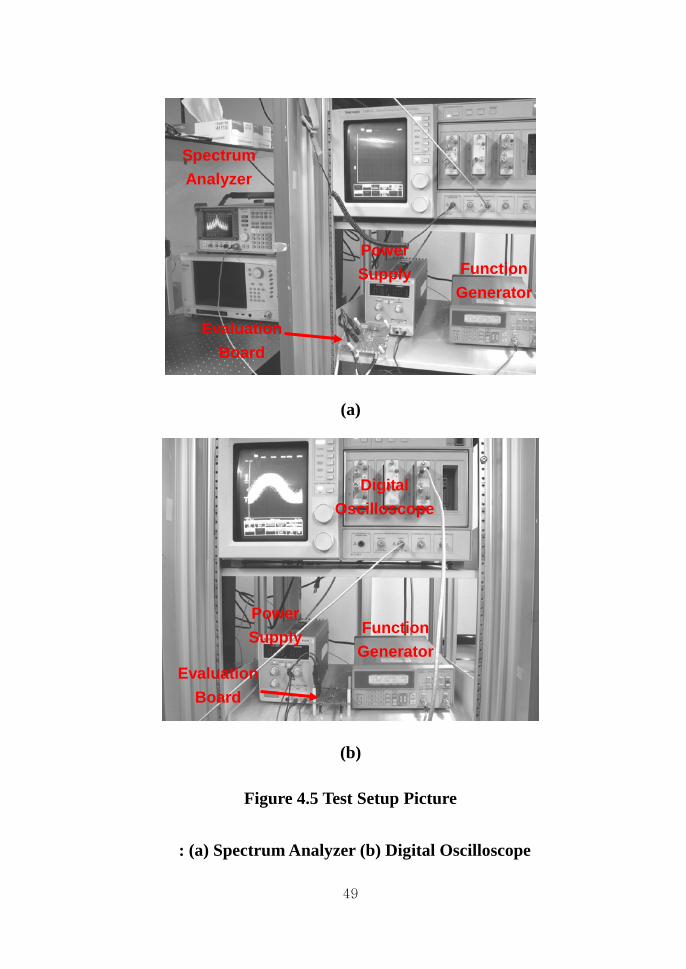
49
(a)
(b)
Figure 4.5 Test Setup Picture
: (a) Spectrum Analyzer (b) Digital Oscilloscope
Digital Oscilloscope
Power Supply Function
Generator Evaluation
Board
Spectrum Analyzer
Function Generator
Power Supply
Evaluation Board

50
4.2.3 VCO Frequency Range Measurement
First of all, it is needed to confirm the frequency range of the VCO.
The control voltage is controlled by changing the variable register.
Figure 4.6 shows the measured frequency range of the VCO. At 2.8V
typical power supply, the frequency range is 450MHz ~ 1.4GHz, and
figure 4.7 shows the frequency error rate that is about 7 ~ -5% in the
VCO tuning range between measurement and post simulation.
The measured VCO frequency range is summarized at table 4.
Table 4 Measurement Result of VCO Frequency Range
Supply Voltage VCO Frequency Range
2.4V 400 MHz ~ 1.1 GHz
2.8V 450 MHz ~ 1.4 GHz
3.2V 500 MHz ~ 1.7 GHz

51
Figure 4.6 Measured VCO Frequency Range
0.0 0.5 1.0 1.5 2.0 2.5-15
-10
-5
0
5
10
15
Erro
r Rat
e [%
]
VCO Voltage [V]
VDD 2.4V VDD 2.8V VDD 3.2V
Figure 4.7 Frequency Error Rate
between Post Simulation and Measurement
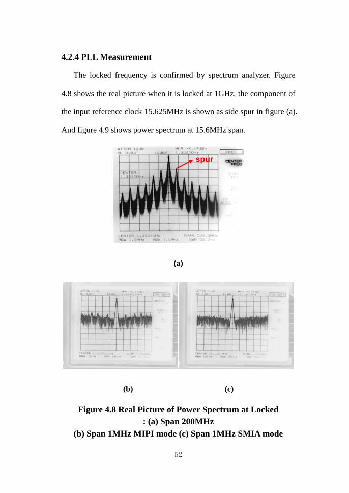
52
4.2.4 PLL Measurement
The locked frequency is confirmed by spectrum analyzer. Figure
4.8 shows the real picture when it is locked at 1GHz, the component of
the input reference clock 15.625MHz is shown as side spur in figure (a).
And figure 4.9 shows power spectrum at 15.6MHz span.
(a)
(b) (c)
Figure 4.8 Real Picture of Power Spectrum at Locked : (a) Span 200MHz
(b) Span 1MHz MIPI mode (c) Span 1MHz SMIA mode
spur

53
992 994 996 998 1000 1002 1004 1006 1008-90
-80
-70
-60
-50
-40
-30
-20
-10
0
dBm
Frequency [MHz]
(a)
642 644 646 648 650 652 654 656 658-90
-80
-70
-60
-50
-40
-30
-20
-10
0
dBm
Frequency [MHz]
(b)
Figure 4.9 Measured Power Spectrum of PLL
: (a) for MIPI (b) for SMIA
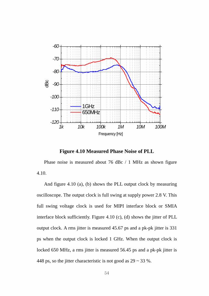
54
1k 10k 100k 1M 10M 100M-120
-110
-100
-90
-80
-70
-60
dB
c
Frequency [Hz]
1GHz 650MHz
Figure 4.10 Measured Phase Noise of PLL
Phase noise is measured about 76 dBc / 1 MHz as shown figure
4.10.
And figure 4.10 (a), (b) shows the PLL output clock by measuring
oscilloscope. The output clock is full swing at supply power 2.8 V. This
full swing voltage clock is used for MIPI interface block or SMIA
interface block sufficiently. Figure 4.10 (c), (d) shows the jitter of PLL
output clock. A rms jitter is measured 45.67 ps and a pk-pk jitter is 331
ps when the output clock is locked 1 GHz. When the output clock is
locked 650 MHz, a rms jitter is measured 56.45 ps and a pk-pk jitter is
448 ps, so the jitter characteristic is not good as 29 ~ 33 %.

55
(a) (b)
(c) (d)
Figure 4.11 Measured Waveform and Jitter
: (a) Waveform at 1 GHz (b) Waveform at 650 MHz
(c) Jitter at 1 GHz (d) Jitter at 650 MHz
Full Swing 2.8V Full Swing 2.8V

56
At this experiment of this PLL, the input reference clock is entered
by common function generator, so this result of the measurement is
cause by the input reference. If the precise clock is used as the input
reference clock, this result of the measurement maybe better than this
result. Table 5 shows the measurement result of this PLL. Duty cycle
and jitter characteristics are not satisfied. Duty cycle problem is solved
by duty correction circuit, and jitter problem is solved by using
regulated supply voltage at VCO block.
Table 5 Measurement Summary
Spec. Design Target Measurement
Result
Power Supply 2.4 ~ 3.2V 2.4 ~ 3.2V
Input frequency 6 ~ 27MHz 10 ~ 16MHz
VCO range 500MHz ~ 1.1GHz 500MHz ~ 1.1GHz
Jitter 5% rms Jitter : 4.5% pk-pk Jitter : 33%
Duty cycle 45 ~ 55% 44%
Locking time ~ 1ms ~ 2.5us
Temperature Range
-20 ~ 60℃ 25℃
57
CHAPTER Ⅴ
Conclusion
In this dissertation, a wide range PLL for MIPI and SMIA interface
at mobile image sensor is designed and fabricated 0.35um thick
transistors in 0.18um mixed CMOS technology.
The designed PLL uses 6 ~ 27MHz external reference clock and
generates 1GHz output clock for MIPI standard interface or 650MHz
output clock for SMIA standard interface. The output clock is 64
divided through dynamic logic divider to meet the input bandwidth. A
VCO is designed 4 stage ring type by PMOS latched delay cell and
operates well at PVT variation at the MIPI and SMIA standard
specifications. A frequency locking time is under 2.5us and power
consumption is 20mW, when this PLL operates at 1GHz, 2.8V power
supply. The core area occupies 121 × 51 um2
The measurement of the designed PLL is tested by measuring VCO
frequency range, locking frequency and jitter. VCO range is measured
500MHz ~ 1.1GHz at 2.4V ~ 3.2V power supply and phase noise is
76cBc/1MHz, and rms jitter is 4.5%, pk-pk jitter is about 30%. If the
jitter characteristic is improved well, this PLL can be adopted at high
.
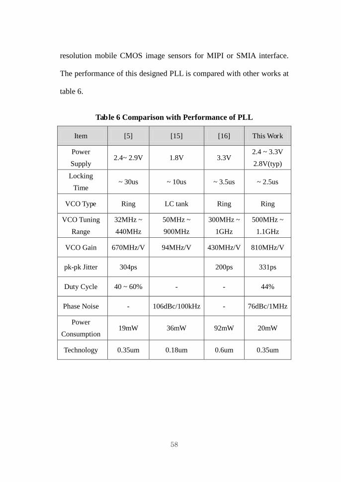
58
resolution mobile CMOS image sensors for MIPI or SMIA interface.
The performance of this designed PLL is compared with other works at
table 6.
Table 6 Comparison with Performance of PLL
Item [5] [15] [16] This Work
Power Supply
2.4~ 2.9V 1.8V 3.3V 2.4 ~ 3.3V 2.8V(typ)
Locking Time
~ 30us ~ 10us ~ 3.5us ~ 2.5us
VCO Type Ring LC tank Ring Ring
VCO Tuning Range
32MHz ~ 440MHz
50MHz ~ 900MHz
300MHz ~ 1GHz
500MHz ~ 1.1GHz
VCO Gain 670MHz/V 94MHz/V 430MHz/V 810MHz/V
pk-pk Jitter 304ps 200ps 331ps
Duty Cycle 40 ~ 60% - - 44%
Phase Noise - 106dBc/100kHz - 76dBc/1MHz
Power Consumption
19mW 36mW 92mW 20mW
Technology 0.35um 0.18um 0.6um 0.35um

59
Bibliography
[1] J. H. Kim, J. C. Shin, C. R. Moon, S. H. Lee, D. C. Park, H. G.
Jeong, D. W. Kwon, J. W. Jung, H. P. Noh, K. B. Lee, K. G. Koh, D. H.
Lee and K. N. Kim, "1/2.5" 8 mega- pixel CMOS Image Sensor with
enhanced image quality for DSC application", IEDM, Dec 2006.
[2] www.mipi.org
[3] M. Y. Eom, J. G. Oh, and S. W. Kim, "Camera Interface Method in Mobile Handset and its Performance Comparison", ICPPW International Conference on, pp. 33-33, Sep 2007.
[4] www.smia-forum.org
[5] Y. W. Lee, “A Low Voltage and Wide Range Phase-Locked Loop for
Standard Mobile Imaging Architecture”, M.S dissertation, Graduate
school of engineering, Yonsei University, Dec 2005.
[6] B. Razavi, “Design of Analog CMOS Integrated Circuits”,
McGrawHill, 2001.

60
[7] P. K. Hanumolu, “Analysis of Charge-Pump Phase_Locked Loops”,
IEEE Transaction on circuits and systems, Vol. 51, pp. 1665-1674, Sep.
2004.
[8] Z. Shu, K. L. Lee, and B. H. Leung, "A 2.4-GHz Ring-Oscillator-
Based CMOS Frequency Synthesizer With a Fractional Divider Dual-
PLL Architecture" IEEE J. Solid-State Circuits, Vol. 39. No. 3, pp. 452-
462, Mar 2004.
[9] E. Gardner, “Charge-pump phase-lock loops”, IEEE Trans.
Commun, Vol. COM-28, pp. 1894-1858, Nov. 1980.
[10] E. H. M and F. Yuan, "An overview of low-voltage delay cells and
a worst-case analysis of supply noise sensitivity", Electrical and
Computer Engineering, 2004. Canadian Conference on,1785-1788 Vol.
3, May 2004
[11] J. S. Lee, "A low-noise fast-lock phase-locked loop with adaptive
bandwidth control ", IEEE Journal of Solid-State Circuit, vol.35. No. 8.
Aug. 2000.

61
[12] J. G. Maneatis and M. A. Horowitz, "Precise Delay Generation
Using Coupled Oscillators", IEEE Journal of Solid-State Circuit, vol.28.
No. 12. Dec 1993.
[13] J. U. Lee, “Research of Gbps Data an d Clock Recovery Circuit” ,
M.S dissertation, Graduate school of engineering, Yonsei University,
Jun 2001.
[14] Y. Ye, “Analysis and simulation three order charge-pump phase-
lock loop”, IEEE international conference on wireless communications,
networking and mobile computing, 12-14, Oct. 2008.
[15] S. O. Ko, “Design of a wide-band cmos frequency synthesizer for
DTV applications”, 2009 SOC conference, session A3.3. May 2009.
[16] H. J. Sung, “A 3.3V cmos dual-looped PLL with a current-
pumping algorithm”, IEICE trans. fundamentals, vol.E83-A. No. 2. Feb
2000.

62
국문요약
모바일 CMOS 이미지 센서용
MIPI와 SMIA 인터페이스 지원을 위한
광대역 위상 동기 루프 설계에 관한 연구
최근 모바일 이미지 센서는 CMOS 공정기술의 발전에 따
라 해상도가 높아지고 있으며 이에 따른 이미지 센서의 출력
을 위한 SMIA 인터페이스와 MIPI 인터페이스를 지원하도록
규정하고 있다. 본 연구에서는 이러한 고해상도 이미지 센서에
사용되는 고속 인터페이스를 지원하는 저전력 및 광대역 위상
동기 루프 설계에 관한 연구이다.
모바일 이미지 센서의 외부 클록인 6 ~ 27MHz의 기준 클록
을 사용하여 MIPI 인터페이스를 지원하기 위한 1GHz 및
SMIA 인터페이스를 지원하기 위한 650MHz의 출력 클록을 얻
기 위해 TSPC 타입의 분주기를 사용하여 64분주하도록 하였
고, 공정변화 및 전압과 온도에도 SMIA용 650MHz에서 MIPI
용 1GHz까지 동작하도록 PMOS Latched delay cell을 4단 연결한

63
RING 타입의 전압조절 발진기를 설계하였으며, 주파수 락킹
시간은 2.5us 이하 및 MIPI 인터페이스용 클록으로 1GHz로 락
킹되어 동작했을 경우 공급전압 2.8V에서 소비전력은 20mW로
설계하였다.
본 연구의 실측 검증을 위하여 0.18um CMOS 표준공정을
사용하여 설계하였으며, 특히 모바일 이미지 센서용으로서 대
기 누설 전류를 최소화 하기 위해 트랜지스터의 게이트 길이
가 0.35um인 Thick CMOS 트랜지스터를 사용하여 설계하였다.
설계된 위상 동기 루프의 측정 결과 주파수 범위는 공급전압
2.4V ~ 3.2V에서 500MHz ~ 1.1GHz의 발진 클록을 확보하였고,
1GHz 및 650MHz에서 Phase noise 측정 결과 76cBc/1MHz를 확
인할 수 있었다. 지터 특성은 1GHz로 동기되었을 때 45.67ps,
650MHz로 동기되었을 때 56.45ps로 측정되었다.