Embed Size (px)
Citation preview
University of Pennsylvania Department of Electrical Engineering
A VLSI COMPUTATIONAL SENSOR FOR THE
DETECTION OF IMAGE FEATURES
Masatoshi Nishimura
A PH.D DISSERTATION
in
Electrical Engineering
Philadelphia, PA 19104
A VLSI COMPUTATIONAL SENSOR FOR THE
DETECTION OF IMAGE FEATURES
Masatoshi Nishimura
A DISSERTATION
in
Electrical Engineering
Presented to the Faculties of the University of Pennsylvania in Partial
Fulfillment of the Requirements for the Degree of Doctor of Philosophy
2001
Jan Van der Spiegel
Supervisor of Dissertation
Kenneth R. Laker
Graduate Group Chairperson

Copyright
Masatoshi Nishimura
2001

iii
Dedicated to Kazuko, Taku, and Mizuki

iv
ACKNOWLEDGEMENT
It has been a long journey. I would really like to thank everyone who helped me reach this
stage.
My first thanks go to my advisor, Professor Van der Spiegel. He gave me the opportunity to
work on this research project and guided me over the years to the point where I am now. I learned a
lot from his vast knowledge and intellectual insight. His encouragement and support were
invaluable for me. I would also like to thank the other members of the committee: Professors
Farhat, Laker, Mueller, and Santiago-Aviles for carefully reading my thesis and giving me
suggestive questions and advice. I wish Professor Ketterer were still alive, from whom I learned the
unique style of thinking. My colleagues, Ralph, Chris, and Pervez, are thanked for their help in
almost every aspect during my stay at Penn. Special thanks to Ralph. You are a good friend.
Thanks for the staff members of the EE department, especially Renee and Lois.
Many people at Sankyo are greatly appreciated. Especially Dr. Saito, for whom I cannot find
words to express my gratitude. He inspired and motivated me to become a good researcher. I would
also like to express my gratitude to Dr. Baba, Dr. Iwata, and Dr. Koike, who gave me the opportunity
to study in the States, and Dr. Nakamura and Dr. Haruyama, who allowed me to continue and
complete my research while staying at Sankyo. I would also like to thank the members of the
medical engineering group and the bioinformatics team. Especially Mr. Sekiya, Mr. Takahashi, Dr.
Nakatsubo, Mr. Niwayama, Mr. Sunamura, Mr. Mizukami, and Dr. Rajniak.
My final thanks go to my family. My wife, Kazuko, has been instrumental for the completion
of my thesis. Without her love, understanding, and constant support, it would have been impossible
for me to reach this point. Also, my two children, Taku and Mizuki, who have always been a great
source of energy for me. I feel like I have completed this thesis with my family altogether.
v
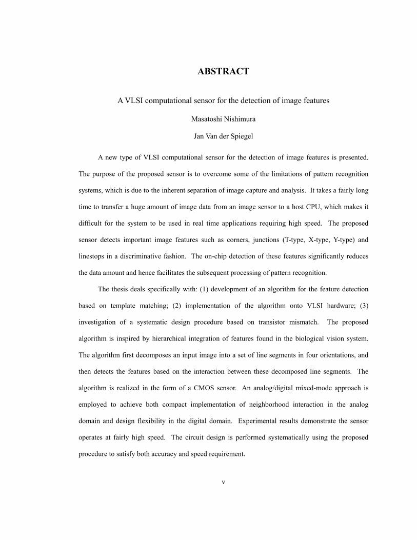
ABSTRACT
A VLSI computational sensor for the detection of image features
Masatoshi Nishimura
Jan Van der Spiegel
A new type of VLSI computational sensor for the detection of image features is presented.
The purpose of the proposed sensor is to overcome some of the limitations of pattern recognition
systems, which is due to the inherent separation of image capture and analysis. It takes a fairly long
time to transfer a huge amount of image data from an image sensor to a host CPU, which makes it
difficult for the system to be used in real time applications requiring high speed. The proposed
sensor detects important image features such as corners, junctions (T-type, X-type, Y-type) and
linestops in a discriminative fashion. The on-chip detection of these features significantly reduces
the data amount and hence facilitates the subsequent processing of pattern recognition.
The thesis deals specifically with: (1) development of an algorithm for the feature detection
based on template matching; (2) implementation of the algorithm onto VLSI hardware; (3)
investigation of a systematic design procedure based on transistor mismatch. The proposed
algorithm is inspired by hierarchical integration of features found in the biological vision system.
The algorithm first decomposes an input image into a set of line segments in four orientations, and
then detects the features based on the interaction between these decomposed line segments. The
algorithm is realized in the form of a CMOS sensor. An analog/digital mixed-mode approach is
employed to achieve both compact implementation of neighborhood interaction in the analog
domain and design flexibility in the digital domain. Experimental results demonstrate the sensor
operates at fairly high speed. The circuit design is performed systematically using the proposed
procedure to satisfy both accuracy and speed requirement.

vi
TABLE OF CONTENTS
Chapter 1 Introduction .................................................................................................. 1
1.1 Research background and motivation .............................................................................. 1
1.2 Contribution of the thesis ................................................................................................. 5
Chapter 2 Algorithm for feature detection .................................................................. 8
2.1 Problem definition............................................................................................................ 8
2.2 Feature detection and pattern recognition in biology ..................................................... 10
2.3 Survey of the algorithms for corner and junction detection ........................................... 17
2.4 Proposed approach ......................................................................................................... 20
2.5 Description of the template matching algorithm............................................................ 24
2.5.1 Basic framework ............................................................................................................ 24
2.5.2 Relationship with other image processing methods....................................................... 31
2.5.3 Implementation considerations ...................................................................................... 37
2.6 Outline of the processing flow ....................................................................................... 39
2.6.1 Overall processing flow ................................................................................................. 39
2.6.2 Thinning......................................................................................................................... 40
2.6.3 Orientation decomposition............................................................................................. 42
2.6.4 Line completion ............................................................................................................. 44
2.6.5 Elimination of isolated points ........................................................................................ 48
2.6.6 Line inhibition................................................................................................................ 50
2.6.7 Line elongation and line thickening............................................................................... 52
2.6.8 Linestop detection.......................................................................................................... 54
2.6.9 Detection of higher level features .................................................................................. 55

vii
2.6.10 Key points of the algorithm ......................................................................................... 61
2.7 Evaluation of the algorithm............................................................................................ 62
2.7.1 Printed characters........................................................................................................... 63
2.7.2 Handwritten characters .................................................................................................. 70
2.7.3 Patterns........................................................................................................................... 71
2.7.4 Discussion...................................................................................................................... 72
2.8 Summary ........................................................................................................................ 74
2.9 References ...................................................................................................................... 75
Chapter 3 Architectural design of the sensor ............................................................ 78
3.1 Overview of related research.......................................................................................... 78
3.1.1 Phototransduction .......................................................................................................... 80
3.1.2 Processing circuit – analog implementation .................................................................. 85
3.1.3 Processing circuit – digital implementation................................................................... 93
3.1.4 Processing circuit – CNN implementation .................................................................... 96
3.1.5 The selected architecture................................................................................................ 97
3.2 Pixel architecture............................................................................................................ 99
3.2.1 Overall architecture...................................................................................................... 100
3.2.2 Phototransistor and thresholding circuit ...................................................................... 101
3.2.3 Processing circuit ......................................................................................................... 103
3.3 Summary ...................................................................................................................... 107
3.4 References .................................................................................................................... 107
Chapter 4 Circuit design based on transistor mismatch analysis .......................... 112
4.1 Problem definition........................................................................................................ 112
4.2 Transistor mismatch ..................................................................................................... 113

viii
4.2.1 Background.................................................................................................................. 113
4.2.2 Formulation of the current variation ............................................................................ 117
4.2.3 Error introduced by current mirror .............................................................................. 122
4.2.4 Error introduced by current summation and subtraction ............................................. 126
4.3 Systematic design procedure for current-mode processing circuits ............................. 132
4.3.1 Background.................................................................................................................. 132
4.3.2 Relationship between error rate and design parameters............................................... 134
4.3.3 Effect of the transistor dimension on the operational speed ........................................ 142
4.3.4 Consideration on the operating region ......................................................................... 148
4.3.5 Simulation using the modified circuit.......................................................................... 153
4.3.6 Final adjustment of the design parameters................................................................... 155
4.3.7 Summary of the design procedure ............................................................................... 156
4.4 Summary ...................................................................................................................... 157
4.5 References .................................................................................................................... 158
Chapter 5 Implementation and experiments ........................................................... 159
5.1 Transient behavior of the circuit .................................................................................. 159
5.2 Mechanisms for high speed operation.......................................................................... 163
5.2.1 High speed charging/discharging mechanism.............................................................. 163
5.2.2 Node locking mechanism............................................................................................. 167
5.3 Control Circuits ............................................................................................................ 170
5.3.1 Two-phase clock generator .......................................................................................... 171
5.3.2 Programmable delay module ....................................................................................... 172
5.3.3 Scanner module............................................................................................................ 174
5.4 Layout and chip fabrication.......................................................................................... 176
5.5 Experiments.................................................................................................................. 177

ix
5.5.1 Testing environment .................................................................................................... 178
5.5.2 Phototransduction ........................................................................................................ 179
5.5.3 Programmable delay module ....................................................................................... 180
5.5.4 Scanner module............................................................................................................ 181
5.5.5 Problems associated with memory configuration ........................................................ 181
5.5.6 Pattern generation ........................................................................................................ 183
5.5.7 Mismatch measurement ............................................................................................... 185
5.5.8 Speed measurement ..................................................................................................... 190
5.5.9 Responses to letter images ........................................................................................... 194
5.5.10 Discussion.................................................................................................................. 197
5.6 Summary ...................................................................................................................... 199
5.7 References .................................................................................................................... 200
Chapter 6 Conclusion................................................................................................. 201

x
LIST OF TABLES
Table 4.1 Matching proportionality constants for difference processes. ................................ 116
Table 4.2 Error rate (%) for o45 detection as a function of the relative current variation. ... 138
Table 4.3 Channel lengths to satisfy the specified accuracy s for different values of Iref. .... 140
Table 5.1 Expected and measured error rate for different values of Iref. ................................ 188
Table 5.2 Execution time required for each operation. .......................................................... 195
Table 5.3 Specifications of the prototype chip....................................................................... 199

xi
LIST OF FIGURES
Figure 1.1 Various shapes of letter “A”. ...................................................................................... 3
Figure 1.2 Two types of pattern recognition systems................................................................... 4
Figure 2.1 Schematic explaining how different types of junctions are generated in different
configurations of objects....................................................................................................... 9
Figure 2.2 Features of interest. ................................................................................................... 10
Figure 2.3 Orientation selectivity of the cell response. .............................................................. 12
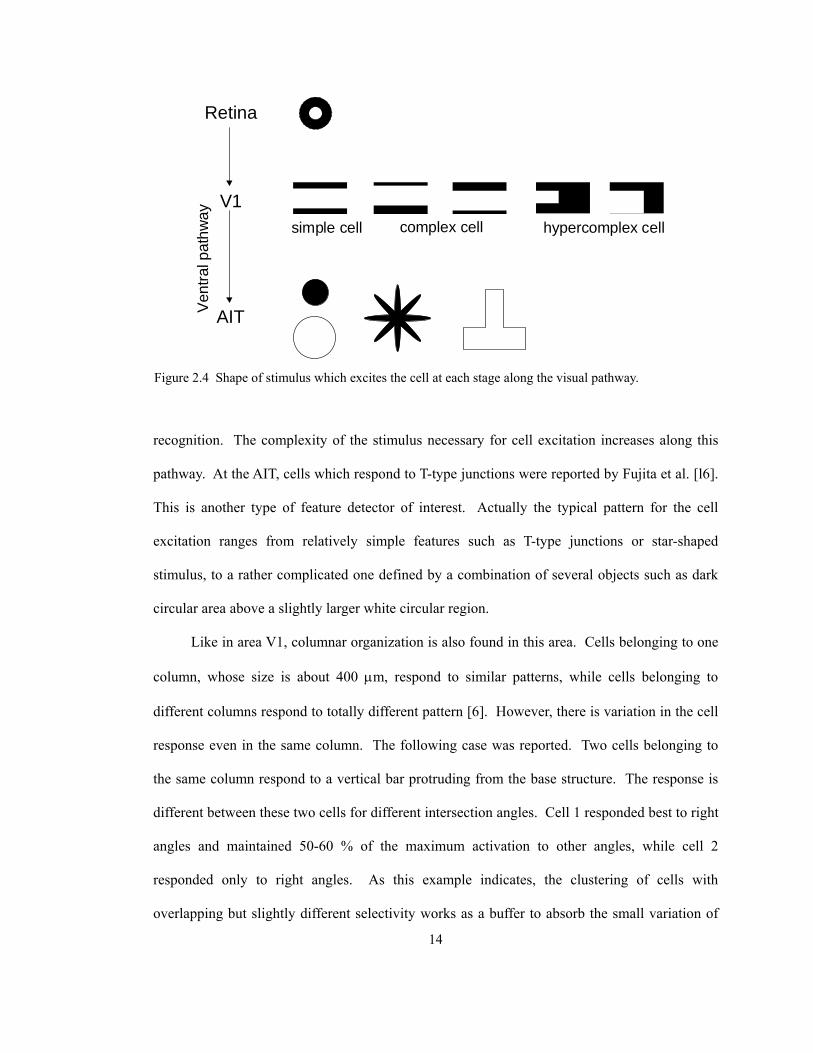
Figure 2.4 Shape of stimulus which excites the cell at each stage along the visual pathway. ... 14
Figure 2.5 Neocognitron model of pattern recognition .............................................................. 16
Figure 2.6 Algorithm for feature detection at a conceptual level. .............................................. 21
Figure 2.7 Venn diagram showing the relationship between the five features detected by the
proposed algorithm. ............................................................................................................ 23
Figure 2.8 Example of template matching. ................................................................................ 26
Figure 2.9 Orientation detection using template matching. ....................................................... 27
Figure 2.10 Linestop detection based on template matching. .................................................... 28
Figure 2.11 Schematic explaining the difficulty of corner detection using a 33 × template..... 30
Figure 2.12 Example of dilation and erosion. ............................................................................ 33
Figure 2.13 Implementation of a convolution kernel. ................................................................ 38
Figure 2.14 Overall processing flow of the feature detection algorithm.................................... 39
Figure 2.15 Algorithm for thinning.. .......................................................................................... 40
Figure 2.16 Example of thinning (one cycle)............................................................................. 41
Figure 2.17 Patterns categorized as o0 with its corresponding template and threshold. ........... 42
Figure 2.18 Patterns categorized as o45 with its corresponding template and threshold. ......... 43

xii
Figure 2.19 Procedure of line completion operation in o0 orientation. ..................................... 45
Figure 2.20 Procedure of line completion operation in o45 orientation. ................................... 47
Figure 2.21 Procedure of elimination of isolated points operation in o0 orientation (top) and in
o45 orientation (bottom). ................................................................................................... 49
Figure 2.22 Procedure of line inhibition operation. ................................................................... 50
Figure 2.23 Schematic explaining the orientation tolerance of the proposed algorithm. ........... 51
Figure 2.24 Line elongation operation and line thickening operation explained for o0 and o45
orientations. ........................................................................................................................ 54
Figure 2.25 Procedure of shrinking............................................................................................ 57
Figure 2.26 Merging of linestops which originally belong to different orientation planes........ 60
Figure 2.27 Features detected by the proposed algorithm for alphabetical characters............... 63
Figure 2.28 Simulation result for letter “V”............................................................................... 64
Figure 2.29 Simulation result for letter “W”. ............................................................................. 65
Figure 2.30 Features detected by the proposed algorithm for italic alphabetical characters. .... 67
Figure 2.31 Pixel point where the stem is separated from the bar of the T-type junction for two
letters “R” and “K”. ............................................................................................................ 68
Figure 2.32 Simulation results for slanted letter “X”. ................................................................ 69
Figure 2.33 Effect of thinning order on the feature detection. ................................................... 70
Figure 2.34 Features detected by the proposed algorithm for handwritten characters. .............. 71
Figure 2.35 Features detected for various patterns..................................................................... 72
Figure 3.1 General architecture of vision sensors. ..................................................................... 79
Figure 3.2 Schematic explaining the process of phototransduction. .......................................... 81
Figure 3.3 Structure of the phototransistor................................................................................. 83
Figure 3.4 Logarithmic compression circuit. ............................................................................. 84

xiii
Figure 3.5 Resistive grid (left) and its impulse response (right). ............................................... 86
Figure 3.6 Conceptual architecture of the pixel circuit. ............................................................. 99
Figure 3.7 Schematic of image digitization circuit with an adjustable threshold current. ....... 101
Figure 3.8 Relationship between the input current and the output current for different switch
settings for the circuit shown in Figure 3.7. ..................................................................... 102
Figure 3.9 Schematic of the processing circuit. ....................................................................... 103
Figure 3.10 Timing diagram for chip operation. ...................................................................... 104
Figure 3.11 Example of an operational sequence..................................................................... 106
Figure 4.1 Current output from a set of transistors that has the common gate voltage. ........... 117
Figure 4.2 Variation of the output currents from a set of transistors with different gate voltages
and process parameters. .................................................................................................... 123
Figure 4.3 Schematic showing the increase of the current variation by current mirror operation.
.......................................................................................................................................... 124
Figure 4.4 Current summation circuit. ..................................................................................... 127
Figure 4.5 The other type of current summation circuit........................................................... 128
Figure 4.6 Generalized current summation circuit. .................................................................. 130
Figure 4.7 Schematic explaining the design flow of the systematic circuit design.................. 134
Figure 4.8 Current thresholding circuit as an example to demonstrate the design procedure.
.......................................................................................................................................... 135
Figure 4.9 Probability distributin function of the output current and the threshold current for
different relative current variations (left: s=0.03; right: s=0.05). ..................................... 137
Figure 4.10 Hspice Monte-Carlo simulation result. ................................................................. 141
Figure 4.11 Schematic to explain the charging and discharging of the capacitance associated
with the gate...................................................................................................................... 142

xiv
Figure 4.12 Relationship between the channel length and the reference current to satisfy
requirements for accuracy and speed................................................................................ 146
Figure 4.13 Relationship between the channel length and the reference current to ensure the
transistor operation in the saturation region. .................................................................... 151
Figure 4.14 Extracted schematic from Figure 3.9 focusing on the current thresholding node.
.......................................................................................................................................... 153
Figure 4.15 Expected and simulated error rate as a function of the reference current. ............ 155
Figure 5.1 Expected evolution pattern when the line completion operation is applied for a
single isolated point. ......................................................................................................... 160
Figure 5.2 Simulation results at the clock frequency of 2.5 MHz............................................ 161
Figure 5.3 Simulation results at the clock frequency of 5 MHz............................................... 162
Figure 5.4 Pixel circuit schematic modified to accelerate the process of charging and
discharging for the critical node Nc. ................................................................................. 163
Figure 5.5 Simulation results at the clock frequency of 5 MHz using the modified circuit
incorporating the high speed charging/discharging mechanism....................................... 164
Figure 5.6 Simulation results at the clock frequency of 10 MHz using the modified circuit
incorporating the high speed charging/discharging mechanism....................................... 166
Figure 5.7 Pixel circuit incorporating the second mechanism for high speed operation.......... 167
Figure 5.8 Simulation results at the clock frequency of 10 MHz using the circuit shown in
Figure 5.7 with the delay between φ2d and φ2 set to 30 nsec............................................. 168
Figure 5.9 Simulation results at the clock frequency of 10 MHz using the circuit shown in
Figure 5.7 with the delay between φ2d and φ2 set to 5 nsec............................................... 169
Figure 5.10 Modified timing diagram incorporating the delay signal φ2d. ............................... 170
Figure 5.11 Schematic of the timing control circuit................................................................. 171

xv
Figure 5.12 Schematic of the two-phase clock generator......................................................... 172
Figure 5.13 Circuit diagram of the programmable delay generator. ........................................ 173
Figure 5.14 Schematic of the scanning circuit. ........................................................................ 174
Figure 5.15 Schematic of the shift register. clk1 and clk2 are non-overlapping two phase
clocks. ............................................................................................................................... 175
Figure 5.16 Layout of the pixel. ............................................................................................... 177
Figure 5.17 Layout of the entire chip. ...................................................................................... 178
Figure 5.18 Schematic of the connection between the test board which contains the test chip
and the PC equipped with a digital I/O board and an A/D converter. .............................. 179
Figure 5.19 Measurement result of the delay of φ2d with respect to φ2 for two power supply
voltages (VDD = 4 V and VDD = 3.3 V). ............................................................................ 180
Figure 5.20 Schematic showing the signal transfer from the thresholding node to the memory.
.......................................................................................................................................... 182
Figure 5.21 Method of generating a grid pattern...................................................................... 184
Figure 5.22 Relative variation of the current as a function of the reference current. ............... 186
Figure 5.23 Schematic explaining the detection error for the linestop detection (LSD)
operation. .......................................................................................................................... 187
Figure 5.24 Maximum operating frequency as a function of the reference current for different
settings of internal delay between φ2 and φ2d. ................................................................... 190
Figure 5.25 Variation of the operating frequency for different error rates............................... 191
Figure 5.26 Maximum operating frequency for three types of operations. .............................. 192
Figure 5.27 Sensor responses to various letter images............................................................. 194
Figure 5.28 Detail of the processing flow for the letter "R"..................................................... 196
1
Chapter 1 Introduction
1.1 Research background and motivation
Vision provides us invaluable information in every part of our life. The information
obtained from an eye is much more direct and appealing than the information obtained from
other sensory organs. This appealing nature is a natural consequence of the tremendous amount
of information obtained as a result of the number of photoreceptors in the retina. There are two
types of photoreceptors, the rods and the cones. The number of rods is 100 million while the
number of cones is 5 million. It is surprising that such a huge amount of information is
processed almost instantaneously to understand the scene surroundings us. It is the researcher’s
dream to build a machine that captures and instantaneously recognizes the image in order to
solve real-world problems.
The goal of building such a machine has been approached from two separate sides:
development of a high quality image sensor and investigation of an algorithm for pattern
recognition. This is just the result of the extreme simplification of treating the retina as an input
device and treating the brain as a processing device. The image sensor, which consists of an
array of photoreceptors, performs phototransduction at each pixel to capture an image. The
number of pixels is increasing year by year, reaching several millions these days, which is
almost comparable to the number of cones. The obtained visual information is then passed onto
a processing system, where various vision algorithms can be performed for pattern recognition.
The above conventional approach for pattern recognition, which consists of image
capture and analysis, has two time consuming steps: the time required for image transfer and the
time required for analysis. The former is determined by the video rate (1/33 msec); the latter is
determined by the amount of data and the algorithm employed. These two time-consuming

2
steps make it difficult for the conventional approach to be used for real-time pattern recognition
such as high-speed product inspection on an assembly line and autonomous navigation. The
problem is the inherent separation between image capture and analysis. It is instructive to look
at the visual information processing system in biology, where the captured information is
processed in an efficient way to recognize the image. A better understanding of the visual
system should be investigated to extract the essence of processing so that it can be mapped onto
hardware in some form.
The essence of the biological vision system is hierarchical integration of features. Along
the visual pathway from the retina to the cortical area, cells in each layer in the hierarchy
function as a detector for a certain image feature. One of the examples is the simple cell and the
complex cell present in the visual cortex. These cells have orientation selectivity and respond to
lines and edges aligned in a particular orientation. There are other cells known to respond to
linestops, corners, and junctions. Features detected in a lower level are integrated in the next-
higher level to represent a more complicated feature. An object is represented as a set of these
features in the final recognition layer. This model of pattern recognition based on hierarchical
feature integration has the following advantages: (1) significant amount of data reduction is
possible, (2) processing is fast due to massive parallelism, (3) recognition is robust to image
deformation.
The above observations lead to new type of image sensors which incorporate some
processing element at each pixel. They can be roughly divided into two categories, analog and
digital, from the point of the type of implementation. The analog implementation is usually
dedicated for a particular purpose while the digital implementation is more general purpose
oriented. What is common for both implementations is the exploitation of parallelism, which is
realized by placing a processing element in each pixel. The on-chip function realized by the
additional processing element extracts relevant information for subsequent processing of pattern

3
recognition, resulting in a reduced amount of data.
The features detected by the analog implementation are primarily edges and orientations.
These are relatively low level features corresponding to those detected at early stages in the
visual pathway. Although the features that can be detected in the digital implementation depend
on the architecture and the programming flexibility, no attempt has been made so far to detect
higher level features such as corners and junctions. Existing software algorithms for these
features are too complicated to be mapped on these digital implementations.
It should be mentioned at this point that while all those implementations incorporate
parallel processing capability, the concept of hierarchical processing, which is another important
characteristic in the biological vision system, is not taken into account. The realization of the
hierarchy in some form may lead to a new type of sensor for the detection of higher level
features. This is the motivation of the research presented in the thesis. The thesis proposes a
new type of computational sensor for the detection of the following features: corners, T-type
junctions, X-type junctions, Y-type junctions, and linestops. These are considered very
important set of features characterizing an object. For example, think about various shapes of
letter “A” shown in Figure 1.1. These four letters are all considered “A” despite its variation in
shape. What is common for these letters is the presence of the corner pointing upward at the
top, T-type junctions on both sides, and two linestops of the vertical line segments at the bottom.
Figure 1.1 Various shapes of letter “A”. Even though the shape is different, all these letter are
categorized as “A”.
4
Such a characterization is not possible simply by using lower level features consisting of edges
and orientations. Therefore, detection of these features is important for the recognition of an
object.
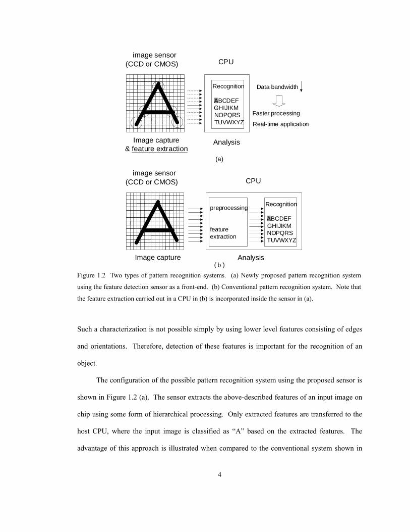
The configuration of the possible pattern recognition system using the proposed sensor is
shown in Figure 1.2 (a). The sensor extracts the above-described features of an input image on
chip using some form of hierarchical processing. Only extracted features are transferred to the
host CPU, where the input image is classified as “A” based on the extracted features. The
advantage of this approach is illustrated when compared to the conventional system shown in
Recognition
ABCDEF GHIJIKM NOPQRS TUVWXYZ
image sensorCPU(CCD or CMOS)
Analysis
preprocessing
feature extraction
Image capture
Recognition
ABCDEF GHIJIKM NOPQRS TUVWXYZ
image sensorCPU(CCD or CMOS)
AnalysisImage capture& feature extraction
Data bandwidth
Faster processing
Real-time application
(a)
(b) Figure 1.2 Two types of pattern recognition systems. (a) Newly proposed pattern recognition system
using the feature detection sensor as a front-end. (b) Conventional pattern recognition system. Note that
the feature extraction carried out in a CPU in (b) is incorporated inside the sensor in (a).

5
Figure 1.2 (b), where all the pixel information is transferred to the CPU. The CPU first
performs feature extraction for the subsequent recognition task. The difference between (a) and
(b) is where preprocessing of feature detection is performed. Feature detection on chip is much
faster than the preprocessing on the CPU since the processing is carried out in a hardware level
in a parallel fashion. Feature detection reduces the data amount, which results in faster data
transfer and facilitates the final recognition task.
Although the above example is specifically for the application of character recognition, it
can be extended for various applications. Think about the case of autonomous navigation. An
autonomous vehicle always has to detect where the road is in front of the vehicle. For this
purpose, the vehicle probably has to detect both sides of the road as well as the centerline,
which are important guidelines for navigation. The vehicle usually keeps following the
centerline. When the vehicle approaches an intersection, it detects the corner on one of the two
sides of the road and makes a turn based on the angle of the corner. For safe navigation,
detection of the centerline with its orientation as well as the corner has to be carried out at high
speed. The proposed sensor will best suit this type of applications. It also has the potential to
have a significant impact on other applications that require high-speed pattern recognition.
1.2 Contribution of the thesis
The thesis examines several aspects concerning the design and implementation of an
image sensor for the detection of the image features. The primary contributions of the thesis
are: (1) development of an algorithm for the feature detection based on template matching; (2)
implementation of the algorithm onto VLSI hardware, (3) investigation of a systematic design
procedure based on transistor mismatch. Each of these contributions is briefly summarized
below.
(1) An algorithm for the detection of image features for a binary image is proposed. The

6
detected features are corners, T-type junctions, X-type junctions, Y-type junctions, and
linestops. No algorithm has been presented which extracts these features in a discriminative
fashion. The proposed algorithm is inspired by the hierarchical integration of features found in
biology. The algorithm first decomposes an input image into a set of line segments in four
orientations, and then detects the features based on the interaction between these decomposed
line segments. With final hardware implementation in mind, the algorithm performs a 3 × 3
template-matching operation in an iterative fashion.
(2) The algorithm is implemented in the form of a CMOS optical sensor. The sensor
contains an array of 16 × 16 pixels, each measuring 150 µm × 150 µm, in a chip area of 3.2
mm × 3.2 mm. The analog/digital mixed-mode architecture is employed to achieve both
compact implementation of 3 × 3 neighborhood interaction in the analog domain and design
flexibility in the digital domain. The internal operation within a 3 × 3 neighborhood is carried
out by the current distribution and thresholding operation. To speed up the operation of the
sensor, a high speed charging/discharging mechanism and another mechanism for node-locking
were implemented. The sensor is able to detect the image features on chip in about 50 µsec.
(3) For the determination of the transistor dimension and the reference current, a
systematic design procedure for current-mode circuits is proposed. The proposed procedure
converts the requirement for accuracy, speed, and the operating region to the specifications for
the transistor dimensions and the reference current. The design parameters are chosen to satisfy
all these three requirements. This procedure is based on the formulation of the current variation
due to transistor mismatch.
The organization of the thesis is as follows. Chapter 2 describes the algorithm for the
feature detection. This chapter includes the survey of biological findings, the mathematical
formulation of the algorithm, and the evaluation of the algorithm. Chapter 3 presents the

7
architectural design of the sensor. Based on the past surveys, an analog/digital mixed mode
architecture is selected. Chapter 4 presents the systematic design procedure for current-mode
processing circuits. Transistor mismatch is analyzed and modeled for the formulation of the
design procedure. Chapter 5 shows implementation details and experimental results obtained
using the prototype sensor to characterize the sensor performance. Finally, Chapter 6 concludes
the thesis.

8
Chapter 2 Algorithm for feature detection
In this chapter, an algorithm for feature detection is described. First, the objective of the
algorithm is defined as the discriminative detection of corners and three types of junctions (T-
type, X-type, Y-type). Then biological findings concerning the visual pathway are surveyed to
confirm the presence of feature detectors and to understand the mechanism of hierarchical
integration for pattern recognition. Existing algorithms for feature detection are also reviewed.
From these observations, the algorithm for feature detection is proposed at a conceptual level.
Then the mathematical framework of template matching in a 3 × 3 neighborhood is presented
to formulate the algorithm. The relationship between template matching and other image
processing methods is also discussed. Based on the framework of template matching, the detail
of the algorithm is described as a sequence of processing flow. The proposed algorithm is
applied to printed and handwritten characters, as well as several patterns, to demonstrate its
performance. Finally, pros and cons of the algorithm are discussed to conclude this chapter.
2.1 Problem definition
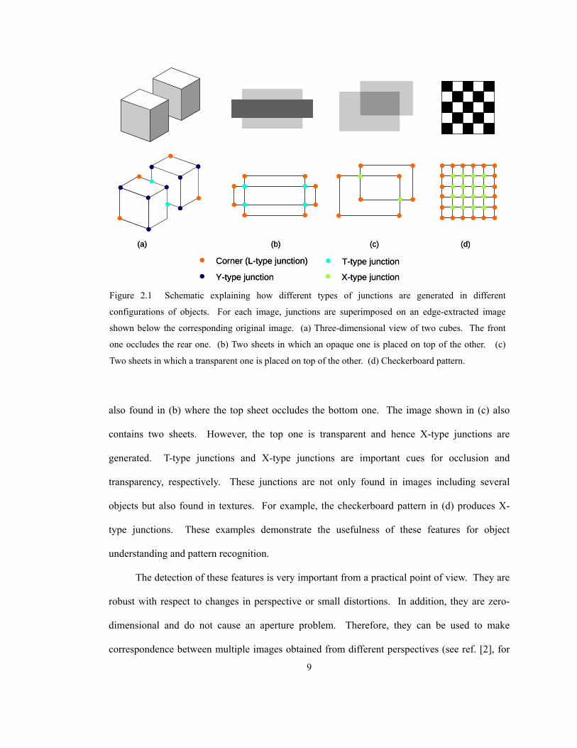
It is well known that corners and junctions carry rich information about the structure of
an object [1]. This is obvious in the example shown in Figure 1.1, where a set of these
geometrical features, together with linestops, characterizes the letter “A”. Another example
demonstrating the significance of these geometrical features for pattern recognition is shown in
Figure 2.1. The three-dimensional view of the two cubes shown in (a) contains corners and
junctions of the Y-type and T-type. Corners and Y-type junctions always exist in the image of a
solid body viewed from a certain angle. The presence of T-type junctions indicates the
occlusion between multiple objects: the rear cube is occluded by the front one. The occlusion is
9
also found in (b) where the top sheet occludes the bottom one. The image shown in (c) also
contains two sheets. However, the top one is transparent and hence X-type junctions are
generated. T-type junctions and X-type junctions are important cues for occlusion and
transparency, respectively. These junctions are not only found in images including several
objects but also found in textures. For example, the checkerboard pattern in (d) produces X-
type junctions. These examples demonstrate the usefulness of these features for object
understanding and pattern recognition.
The detection of these features is very important from a practical point of view. They are
robust with respect to changes in perspective or small distortions. In addition, they are zero-
dimensional and do not cause an aperture problem. Therefore, they can be used to make
correspondence between multiple images obtained from different perspectives (see ref. [2], for
Corner (L-type junction)
Y-type junction
T-type junction
X-type junction
(a) (b) (c) (d)
Corner (L-type junction)
Y-type junction
T-type junction
X-type junction
(a) (b) (c) (d)
Figure 2.1 Schematic explaining how different types of junctions are generated in different
configurations of objects. For each image, junctions are superimposed on an edge-extracted image
shown below the corresponding original image. (a) Three-dimensional view of two cubes. The front
one occludes the rear one. (b) Two sheets in which an opaque one is placed on top of the other. (c)
Two sheets in which a transparent one is placed on top of the other. (d) Checkerboard pattern.

10
example). Although corner detection in real-world problems should deal with a gray image,
once edges are properly extracted in a preprocessing stage, the problem can be simplified as the
detection of these features for an edge extracted image. Then the situation becomes somewhat
similar to that shown in Figure 1.1, where the features are detected for characters, which are
basically line drawings. For this reason, the thesis focuses on binary images, i.e, black and
white images, especially characters, which are considered good examples of line drawings.
Characters are also suitable to test the performance of the algorithm since there are many
variations and deformations. The features we would like to identify are listed in Figure 2.2.
Note that linestops are included in this feature set. It is important to be able to detect these
features for line drawings with any line width.
To summarize, the objective of the algorithm is to detect and locate these features
(corners, T-type, X-type, and Y-type junctions, linestops) in a discriminative fashion for a binary
image. It is also important for the algorithm to be relatively simple so that it can be eventually
implemented in hardware.
2.2 Feature detection and pattern recognition in biology
Since our primary objective is the detection of corners and junctions, it should be helpful
and suggestive to investigate if there are detectors for these features in biological vision system.
If that is the case, how is an object recognized based on these features? In the following,
several biological findings are described to introduce different levels of feature detectors present
(a) (b) (c) (d) (e) Figure 2.2 Features of interest. (a) Corner. (b) T-type junction. (c) X-type junction. (d) Y-type
junction. (e) Linestop.
11
in the visual pathway and their possible role in pattern recognition.
The visual information processing starts at the retina where the intensity of an incoming
light is converted to an electrical signal. Phototransduction is carried out by two types of
photoreceptor cells, the cone and the rod. The cone is responsible for day vision while the rod
is responsible for night vision. The number of the cone is 5 million while the number of the rod
is 100 million [3]. In addition to these two cells, there are four other types of cells in the retina:
the horizontal cell, the bipolar cell, the amacrine cell, and the ganglion cell. These cells belong
to one of the two layers, inner plexiform layer and outer plexiform layer, depending on their
physical location. The outer plexiform layer consists of the photoreceptors (rods and cones), the
horizontal cells, and the bipolar cells, while the inner plexiform layer consists of the amacrine
cells and the ganglion cells.
In the outer plexiform layer, the cones and the rods are connected to the horizontal cells
as well as to the bipolar cells. The horizontal cells, which are mutually connected in a lateral
direction, spread the input signal from the photoreceptors and hence produce a spatially
smoothed version of the incoming signal. The bipolar cell receives excitatory inputs from the
photoreceptors and inhibitory inputs from the horizontal cells, and thus produces an output that
is equal to the difference between the photoreceptor signal and the horizontal cell signal. This
results in a concentric ON-center type receptive field1. The ON-center receptive field indicates
that the light that falls onto the center area of the receptive field excites the bipolar cell while
the light that falls onto the periphery inhibits the bipolar cell. Already at this level in the visual
information pathway, a preliminary level of feature detection is performed: the bipolar cell
responds to edges of an object where intensity changes sharply, while it responds poorly to
uniform illumination [4].
1 The receptive field of a neuron is defined as the area on the retina that affects the signaling of the
neuron.
12
Further signal modification and integration are carried out in the inner plexiform layer to
produce an output at the ganglion cell, which serves as the final station of the retinal processing.
The activity of the ganglion cell seems to be made up by the total contribution of the other four
cell types. The receptive field of the ganglion cell takes an ON-center shape, which is almost
similar to that of the bipolar cell. The difference is that the output is represented by the firing
frequency at the ganglion cell while the output is represented simply by the level of the potential
at the bipolar cell.
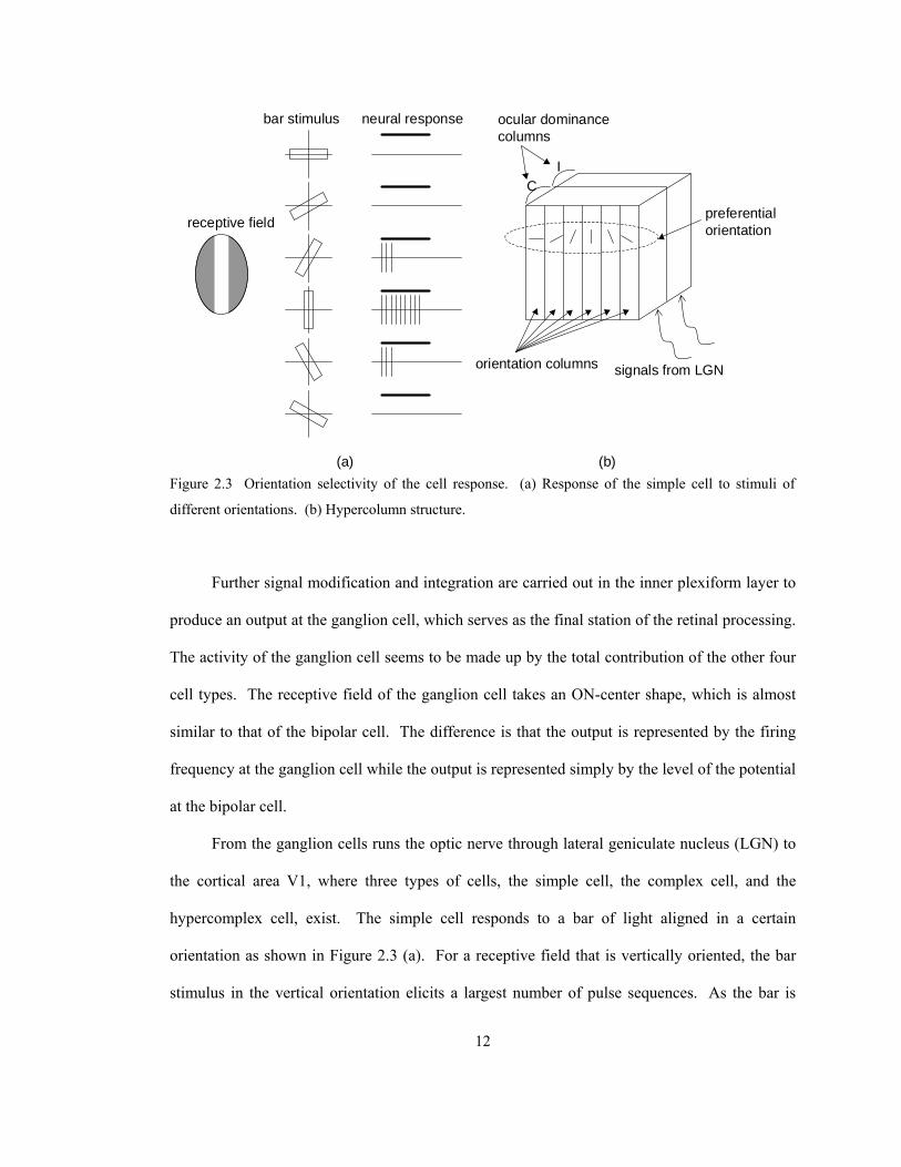
From the ganglion cells runs the optic nerve through lateral geniculate nucleus (LGN) to
the cortical area V1, where three types of cells, the simple cell, the complex cell, and the
hypercomplex cell, exist. The simple cell responds to a bar of light aligned in a certain
orientation as shown in Figure 2.3 (a). For a receptive field that is vertically oriented, the bar
stimulus in the vertical orientation elicits a largest number of pulse sequences. As the bar is
signals from LGN
receptive field
bar stimulus neural response
(a) (b)
orientation columns
ocular dominance columns
CI
preferentialorientation
Figure 2.3 Orientation selectivity of the cell response. (a) Response of the simple cell to stimuli of
different orientations. (b) Hypercolumn structure.

13
rotated from this preferential orientation, the response decreases quickly. This is quite different
from the response of the ganglion cell, which does not have any orientation selectivity. The
complex cell, like the simple cell, also responds to stimulus aligned in a certain orientation.
However, the demand for precise positioning found in the simple cell is relaxed in the complex
cell. As long as a properly oriented stimulus falls within the boundary of the receptive field, the
complex cell responds. The third type of cell, the hypercomplex cell, needs more refined shape
of stimulus for excitation. They require that the stimulus have discontinuity. The simple line
stimulus, even if it is aligned in the preferential orientation, does not excite the cell completely.
Consequently the best stimulus results in linestops and corners (they are also called the
endstopped cell for this reason). This is one of the feature detectors that is interest to us.
The receptive fields of these cells in area V1 are not arranged in a random order: there is
a clear retinotopic mapping present such that adjacent cells have adjacent receptive field
positions in the retina. Orientation selectivity also has a nonrandom arrangement: there are
vertical columns through the thickness of the cortical sheet containing cells with similar
orientation preferences. Each column is about 30-100 µm wide and 2 mm deep. The
preferential orientation shifts from one column to the next column by about o10 . A set of these
columns, which covers the entire orientation, is termed hypercolumn by its discoverer Hubel
and Wiesel [5] (see Figure 2.3 (b)). Each local area in the retinotopic map has a corresponding
hypercolumn. It should be also noted that the cortical cells in area V1 do not respond to
uniform illumination. Therefore, in area V1, these cortical cells extract edges or contour of an
object and represent it as a set of line segments in different orientations.
The extracted information is further transferred from area V1 to V4, thereafter to the
posterior part of inferotemporal cortex (PIT), and finally to the anterior part of inferotemporal
cortex (AIT) through the ventral pathway, which is believed to be responsible for object
14
recognition. The complexity of the stimulus necessary for cell excitation increases along this
pathway. At the AIT, cells which respond to T-type junctions were reported by Fujita et al. [l6].
This is another type of feature detector of interest. Actually the typical pattern for the cell
excitation ranges from relatively simple features such as T-type junctions or star-shaped
stimulus, to a rather complicated one defined by a combination of several objects such as dark
circular area above a slightly larger white circular region.
Like in area V1, columnar organization is also found in this area. Cells belonging to one
column, whose size is about 400 µm, respond to similar patterns, while cells belonging to
different columns respond to totally different pattern [6]. However, there is variation in the cell
response even in the same column. The following case was reported. Two cells belonging to
the same column respond to a vertical bar protruding from the base structure. The response is
different between these two cells for different intersection angles. Cell 1 responded best to right
angles and maintained 50-60 % of the maximum activation to other angles, while cell 2
responded only to right angles. As this example indicates, the clustering of cells with
overlapping but slightly different selectivity works as a buffer to absorb the small variation of
Retina
hypercomplex cell
Ven
tral
pat
hway
V1
AIT
simple cell complex cell
Figure 2.4 Shape of stimulus which excites the cell at each stage along the visual pathway.
15
the input pattern [7]. These observations lead to the following hypothesis: an object is probably
represented in the AIT by a set of activated columns, each corresponding to different patterns,
with some variations allowed within each column.
As explained above, the complexity of the stimulus for cell excitation increases toward
the higher levels in the hierarchy, which is schematically shown in Figure 2.4. The size of the
receptive field also increases as the complexity of the stimulus increases. The increase in the
complexity is achieved by combining the output form several cells having different selectivity at
earlier stages in the visual pathway. For example, the orientation selectivity of the simple cell
can be obtained by combining the output of the ganglion cell aligned in a certain orientation.
The response of the complex cell can be obtained as the combination of the simple cells having
the same orientation selectivity but with different spatial positions. During the process of
feature integration, the position of a particular feature necessary to excite the cell in the next
layer is allowed to shift to some extent. The positional tolerance at each level in the hierarchy
leads to a large variation in the input pattern for cell excitation in the final recognition stage.
This is how the cell in the AIT achieves shift invariance. The response of the cell is essentially
constant throughout its receptive field, which is much larger than that in the earlier stages in the
visual pathway.
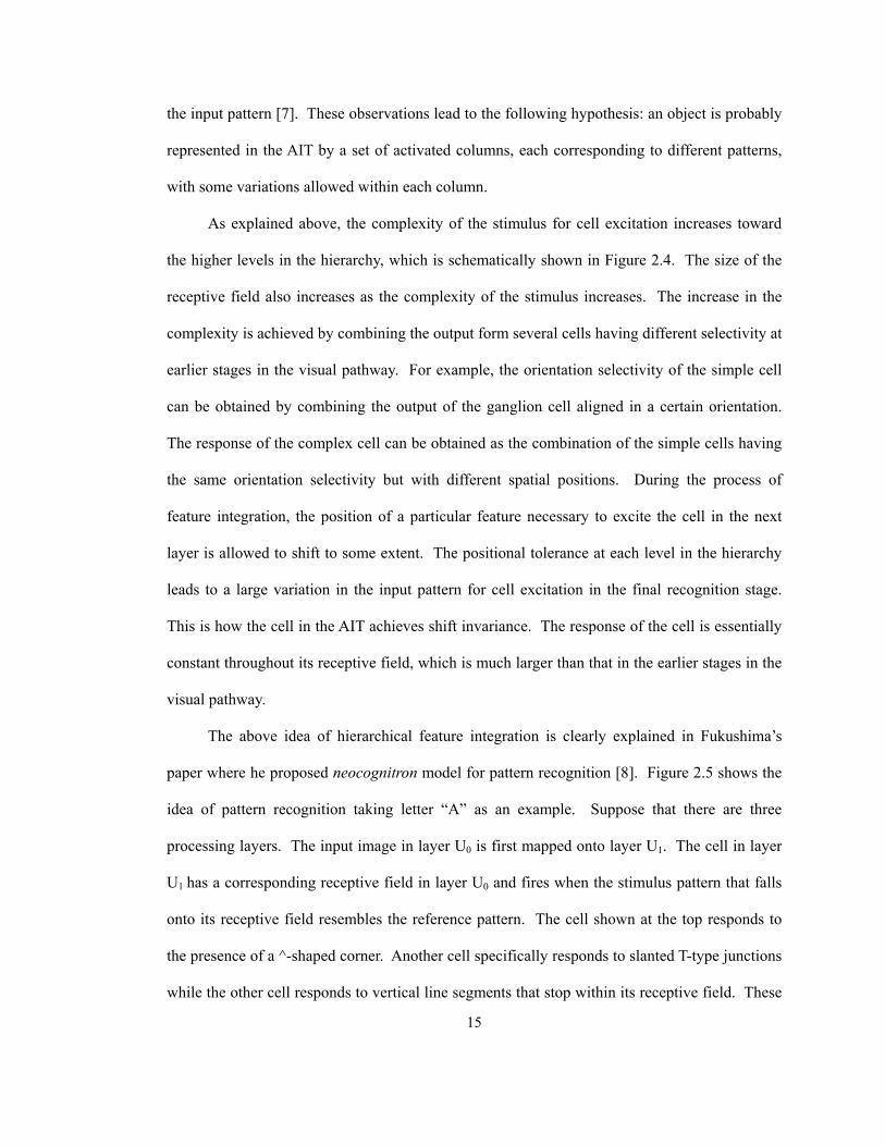
The above idea of hierarchical feature integration is clearly explained in Fukushima’s
paper where he proposed neocognitron model for pattern recognition [8]. Figure 2.5 shows the
idea of pattern recognition taking letter “A” as an example. Suppose that there are three
processing layers. The input image in layer U0 is first mapped onto layer U1. The cell in layer
U1 has a corresponding receptive field in layer U0 and fires when the stimulus pattern that falls
onto its receptive field resembles the reference pattern. The cell shown at the top responds to
the presence of a ^-shaped corner. Another cell specifically responds to slanted T-type junctions
while the other cell responds to vertical line segments that stop within its receptive field. These
16
features are further integrated in layer U2. The cell at the top responds to the stimulus which has
a combination of a ^-shaped corner at the top and two slanted T-type junctions with opposite
directions at the bottom. Likewise, there exist cells in layer U2, which detect a combination of
slanted T-shape junction and a linestop of the vertical line. In the final recognition layer U3,
features are further integrated to generate a cell that is excited by the presence of all three
features in the preceding layer U2. The resultant requirement to excite the cell in layer U3 is that
there is a ^-shaped corner at the top, two slanted T-type junctions on both sides, and two
linestops of a vertical line segments at the bottom, which extracts the essence of letter “A”. In
other words, the letter “A” is characterized by a set of these features.
Representation of an object by a set of features results in a significant amount of data
compression. In addition, by allowing some positional tolerance for a feature at each level in
the hierarchy, the final layer is able to recognize deformed letters “A”. It should be also noted
that the whole processing is carried out in a massively parallel fashion, resulting in an enormous
amount of computational power even it is performed by slowly operating neurons.
To summarize this section, the biological vision system is characterized by hierarchical
U0 U1 U2 U3 Figure 2.5 Neocognitron model of pattern recognition (adapted from Fukushima [8] and slightly
modified).

17
integration of features. Detectors for corners and junctions do exist in this hierarchy. These
features are formed from lower level features such as edges or linestops in different orientations,
and they are further integrated to higher level features to finally represent an object as a set of
these higher level features. These observations not only confirm the importance of the detection
of corners and junctions for pattern recognition, but also give some clue for the implementation
of these features.
2.3 Survey of the algorithms for corner and junction detection
Having understood the importance of corners and junctions in pattern recognition and the
presence of detectors for these features, we are ready to implement these feature detectors
borrowing some ideas from biology. Before going into detail, however, several algorithms for
detection of these features, some of which are biology based and some of which are not, are
briefly discussed below.
Fukushima implicitly implemented detectors for corners and junctions in his later work
[9], where he applied the neocognitron concept to the character recognition problem in the form
of a five-layered neural network. To form the receptive field of different complexities in
different layers, appropriate patterns are used to train each layer. The second layer is trained to
respond to line segments in eight orientations ( o0 , o5.22 , o45 , L , o5.157 ). The third layer is
trained to respond to different combinations of the line segments detected in the second layer,
which represents corners with different angles and junctions of different types (T-type, X-type,
Y-type). The trained network was able to correctly classify input patterns even with its position
shifted or with its shape deformed. Although this work demonstrates the excellent example of
the neural network architecture for pattern recognition, these types of feature detectors do not
explicitly detect and locate the position of features and do not fit our interest.
18
Actually within the framework of the neural network, explicit implementation of feature
detectors other than oriented line segments and linestops have not been reported (for example,
see refs. [10], [11], [12]). This is because the direct detection of corners and junctions is not as
simple as it first looks, which is explained in Section 2.5.
Heitger et al. have proposed an “endstopped operator”, which mimics the function of the
endstopped cell in the visual system [13]. They first convolved an input image with even and
odd symmetrical orientation selective filters and combined the output of these two filters to
compute a local energy measure. The output image corresponds to the output of the complex
cell, where edges and lines are enhanced in a preferential orientation. Then the differentiation
(the first derivative and the second derivative) of this output image is calculated along the
preferential orientation. The local maxima of combined endstopped operators for all
orientations indicate the position of what they call “key-points”. The simulation result showed
that the endstopped operator was able to detect linestops, corners, and T-type junctions. The
detector would be able to detect Y-type junctions with less specificity. However, it would be
difficult to detect X-type junctions because they do not produce a local maximum at these
points.
Freeman also applied the similar approach for the detection of corners, T-type junctions
and X-type junctions [14]. His method computes the local energy along multiple orientations to
find two dominant orientations along which edges are represented. Then the stopped-ness is
calculated as the derivative along these two orientations. If stopped-ness is high in two
orientations, the junction is detected as the corner. If stopped-ness is low in one of the two
orientations, it is classified as the T-type junction. If stopped-ness is not low in both
orientations, the junction is classified as the X-type junction. In other words, this method keeps
the orientation information and defines the type of junctions based on how the components in
two orientations interact with each other. The only restriction for this method is that the number
19
of dominant orientations is limited to two, which would make it difficult to find Y-type
junctions.
Dobbins et al. have modeled the output of the hypercomplex (endstopped) cell as the
difference of two simple cells with a different size of the receptive field. This operation results
in the receptive field that has the excitatory center zone and the inhibitory zone at both ends,
which is similar to the result of the second derivative along the preferential orientation. The
modeled endstopped cell showed the curvature dependent response [15] [16]. Manjunath et al.
have proposed an almost similar approach and applied their method for practical applications
such as face recognition, image registration, and motion estimation [2].
Apart from these biology-based approaches, there are two popular methods for corner
detection. One is what is known as Plessey detector proposed by Harris and Stephens [17]
while the other is known as SUSAN detector proposed by Smith and Brady [18]. The Plessey
detector calculates the derivative of image intensities and defines the average squared gradient
matrix. The feature is detected as the point where a certain measure computed from the average
squared gradient matrix takes a local maximum in the image plane. Although this algorithm can
detect corners and three types of junctions (T-type, X-type, Y-type), the detected point does not
exactly coincide with the true location of these features. The performance of the SUSAN
detector is superior in this sense. The SUSAN algorithm defines a circular area for each point
with the center of the circle located on that point and counts the number of pixels within the
circle which has the same intensity as the center. Note that no derivative is computed in this
algorithm, which gives superior noise immunity [18]. The counted number takes a maximum
value in the uniform region and decreases to its half at straight edge points and decreases even
more at corners and junctions. Thus, these features are detected by finding local minima of the
counted number. One of the possible problems of this method is that it does not seem to work
for binary edge images. Also, note that no orientation information is attached to the detected

20
feature points. Consequently, the determination of the junction type is difficult.
All the methods so far described perform computation locally. For line drawings, there
are other methods proposed which need searching neighborhood pixels along the line segment.
See refs. [19], [20], and [21], for example. These methods require lots of computation but still
cannot detect junctions very well.
2.4 Proposed approach
Each algorithm surveyed in the previous section has its advantages and disadvantages.
The only method to partly satisfy the demand of discriminative identification of corners and
junctions is Freeman’s method despite its expected difficulty for the detection of Y-type
junctions. The other methods cannot discriminate corners and junctions. Freeman’s method is
biology based in the sense that orientation decomposition with simultaneous edge extraction is
performed as preprocessing.
Having a look at Figure 2.2 again, it is obvious that these five features are defined as a
result of interaction between line segments and linestops of different orientations. The corner is
defined as the point where two line segments of different orientations meet at its linestop. The
T-type junction is defined as the point where the linestop of a line segment meets another line
segment of different orientation. The X-type junction is defined as the point where at least two
line segments of different orientations meet. The Y-type junction is defined as the point where
at least three line segments of different orientations meet at its linestop. This simple definition
of these features leads to the conceptual processing flow of the proposed algorithm, which is
shown in Figure 2.6. The algorithm finally produces the five features, which are shown in the
boxes with a thick boundary line, after several steps of hierarchical processing based on
orientation decomposition.
The first processing is the thinning of an input image. Thinning is a process of reducing
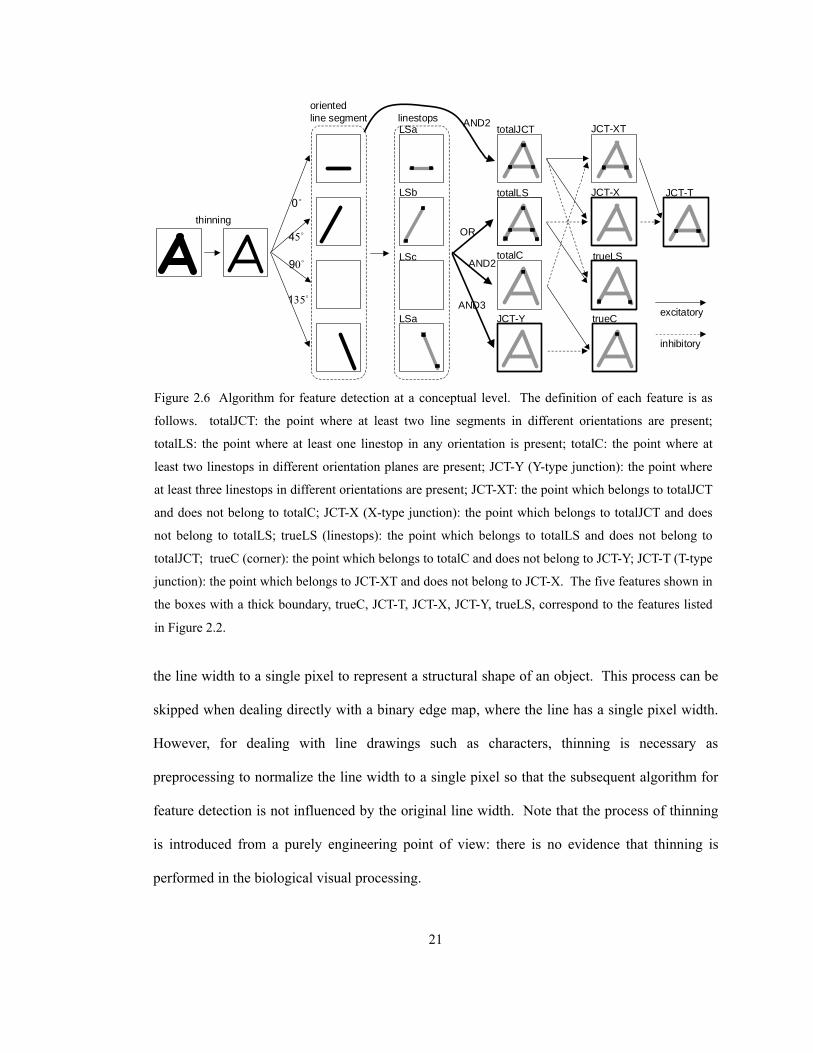
21
the line width to a single pixel to represent a structural shape of an object. This process can be
skipped when dealing directly with a binary edge map, where the line has a single pixel width.
However, for dealing with line drawings such as characters, thinning is necessary as
preprocessing to normalize the line width to a single pixel so that the subsequent algorithm for
feature detection is not influenced by the original line width. Note that the process of thinning
is introduced from a purely engineering point of view: there is no evidence that thinning is
performed in the biological visual processing.
linestopsJCT-XT
thinning
AND2
OR
LSa
AND2
oriented line segment
AND3
totalC
totalLS
JCT-Y
JCT-X JCT-T
trueLS
trueC
LSb
LSa
LSc
o0
o54
o09
o351
totalJCT
excitatory
inhibitory
Figure 2.6 Algorithm for feature detection at a conceptual level. The definition of each feature is as
follows. totalJCT: the point where at least two line segments in different orientations are present;
totalLS: the point where at least one linestop in any orientation is present; totalC: the point where at
least two linestops in different orientation planes are present; JCT-Y (Y-type junction): the point where
at least three linestops in different orientations are present; JCT-XT: the point which belongs to totalJCT
and does not belong to totalC; JCT-X (X-type junction): the point which belongs to totalJCT and does
not belong to totalLS; trueLS (linestops): the point which belongs to totalLS and does not belong to
totalJCT; trueC (corner): the point which belongs to totalC and does not belong to JCT-Y; JCT-T (T-type
junction): the point which belongs to JCT-XT and does not belong to JCT-X. The five features shown in
the boxes with a thick boundary, trueC, JCT-T, JCT-X, JCT-Y, trueLS, correspond to the features listed
in Figure 2.2.
22
The thinned pattern is decomposed into four orientation planes, i.e., o0 , o45 , o90 , and
o135 orientation planes, each of which contains line segments of the designated orientation. For
example, letter “A” is decomposed into three line segments of different orientations, o0 , o45 ,
and o135 orientations. Note that there is orientation tolerance to some degree: each line segment
is classified into one of the four orientations that is closest to its orientation. The orientation
decomposition can be considered a simplified realization of the processing which takes place at
the hypercolumn in the brain, although the resolution of orientation decomposition is o45 ,
which is much lower than that found in the hypercolumn.
The next processing after orientation decomposition is the detection of linestops for each
line segment. This processing corresponds to that of the hypercomplex cell (endstopped cell) in
biology. Then based on the oriented line segments and linestops, higher level features are
computed as described below. totalJCT is defined as the point where at least two line segments
in different orientations are present. The operation for this detection is designated as AND2 in
the figure: AND2 operation sets the pixel value to 1 where at least two pixels whose value is 1
are present among the four orientations. For letter “A”, totalJCT includes two junctions on both
sides and the corner at the top. In contrast to totalJCT, which are derived from oriented line
segments, the other three features, totalLS, totalC, and JCT-Y, are detected from linestops.
totalLS is detected as the point where at least one linestop in any orientation plane is present,
which is obtained by OR operation for four linestop images (LSa, LSb, LSc, LSd) as shown in
the figure. Likewise, totalC is defined as the point where at least two linestops in different
orientations are present, which is obtained by AND2 operation. JCT-Y is defined as the point
where at least three linestops in different orientations are present, which is obtained by AND3
operation. JCT-Y is one of those finally detected five features (Y-type junction). Note that
totalLS includes totalC as its subset, which further includes JCT-Y as its subset.
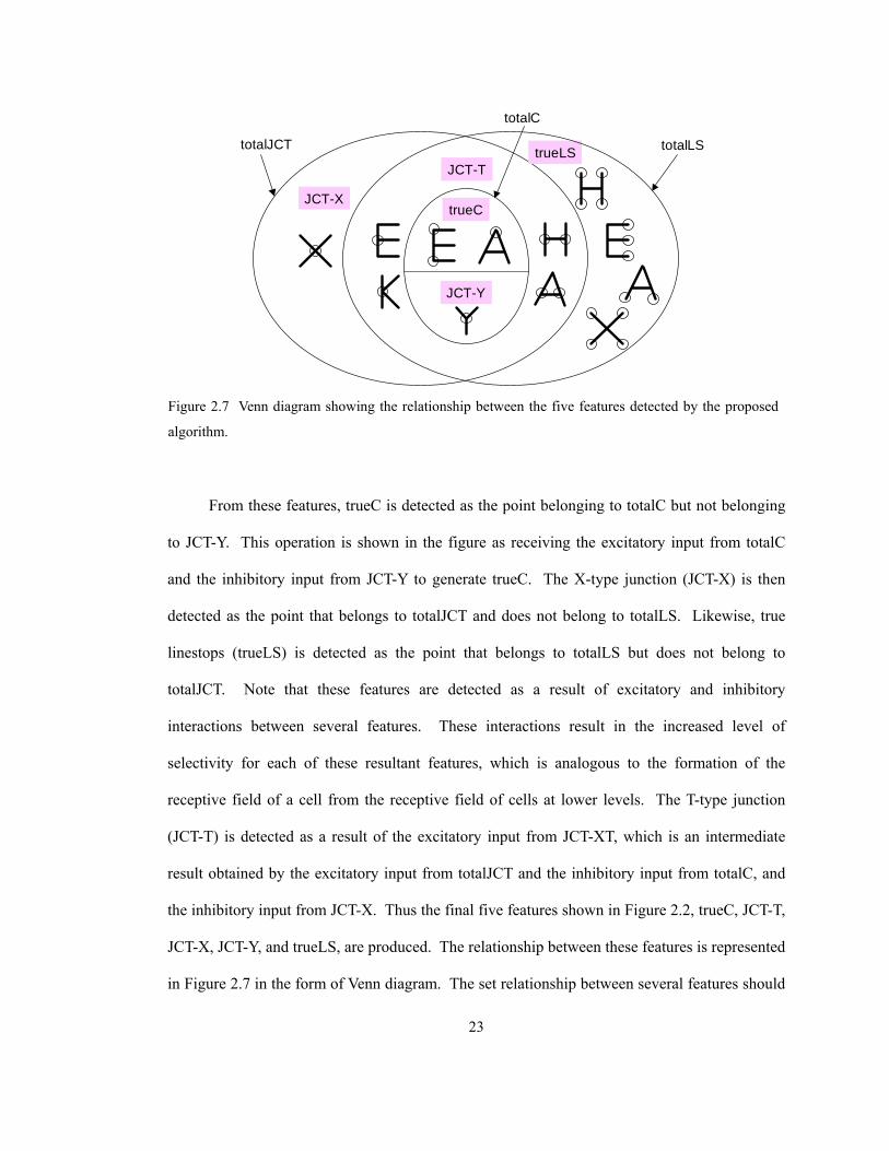
23
From these features, trueC is detected as the point belonging to totalC but not belonging
to JCT-Y. This operation is shown in the figure as receiving the excitatory input from totalC
and the inhibitory input from JCT-Y to generate trueC. The X-type junction (JCT-X) is then
detected as the point that belongs to totalJCT and does not belong to totalLS. Likewise, true
linestops (trueLS) is detected as the point that belongs to totalLS but does not belong to
totalJCT. Note that these features are detected as a result of excitatory and inhibitory
interactions between several features. These interactions result in the increased level of
selectivity for each of these resultant features, which is analogous to the formation of the
receptive field of a cell from the receptive field of cells at lower levels. The T-type junction
(JCT-T) is detected as a result of the excitatory input from JCT-XT, which is an intermediate
result obtained by the excitatory input from totalJCT and the inhibitory input from totalC, and
the inhibitory input from JCT-X. Thus the final five features shown in Figure 2.2, trueC, JCT-T,
JCT-X, JCT-Y, and trueLS, are produced. The relationship between these features is represented
in Figure 2.7 in the form of Venn diagram. The set relationship between several features should
totalJCT
JCT-X
totalLStrueLS
totalC
trueC
JCT-Y
JCT-T
Figure 2.7 Venn diagram showing the relationship between the five features detected by the proposed
algorithm.

24
be associated with the excitatory and inhibitory arrows shown in Figure 2.6.
2.5 Description of the template matching algorithm
In the previous section, an algorithm for feature detection is described at a conceptual
level. To formulate the algorithm, the mathematical framework of template matching is given
in this section.
2.5.1 Basic framework
The mathematical framework employed in the thesis to formulate the algorithm is
template matching in a 33× window. For a given input image, the updated image is computed
as follows. For every pixel in the input image, the updated status is set to 1 if its 33×
neighbors match the given template with some specified tolerance, and is otherwise set to 0.
This procedure is mathematically represented as
∑ ∑−= −=
++=+1
1
1
1, );)(()1(
l mlmmjliij Irnxfnx (2.1)
where )(nxij is the binary status of the pixel at the position (i,j) at a discrete instant n, ijr is the
element of the template, f is the function to generate a binary output using the threshold I given
in the form below:
<≥
=.for0
for1);(
IxIx
Ixf (2.2)
The template is represented as
=
−
−−
−−−−
110111
100010
110111
rrrrrrrrr
R . (2.3)
Each element of the template takes one of the following three values: 1− , 0, or 1. Value of 1
imposes that the pixel value at the corresponding position should be 1; Value of 1− imposes

25
that the pixel value at the corresponding position should be 0; Value of 0 does not impose any
restriction for the corresponding pixel position (“don’t care”). For simplicity, let us denote the
template matching using the template R and the threshold I as
))(()1( , nXTnX IR=+ (2.4)
where X(n) represents the whole image plane, i.e., a whole set of xij(n), at instant n.
The implication of the above computation is briefly explained below. Template matching
is nothing but the calculation of correlation. First, at any position in the image plane, the
correlation between its 33× neighbors and the template is calculated: each element is
multiplied by the correspondong coefficient in the template R and the result is accumulated.
Then the accumulated result is compared to the threshold I to digitize the output. Depending on
how to construct the template and the threshold value, the strictness of the template matching
can be controlled as shown in Figure 2.8.
The first example shown in (a) demonstrates the case of exact matching: the template
does not contain 0 and the threshold is 4.5, which is smaller than the number of pixels whose
value is 1 by one half. Only the center of the cross on the top left corner in the image plane is
kept in the updated image, since the correlation result is 5 and is greater than the threshold only
at this point. Any other point in the image plane is not selected. The only possible pattern to
satisfy the criteria for selection is the template itself with its –1 element interpreted as 0.
The incorporation of 0 in the template gives “don’t care” condition to the pixel value at
the corresponding position as shown in Figure 2.8 (b). This is the first level of stringency
control in template matching. Since the pixel value at the “don’t care” position does not
contribute to the correlation computation, the bottom left pattern in the image plane, is selected
in the updated image. The second level of stringency control in template matching is realized
by the decrease in the threshold value as shown in Figure 2.8 (c), where the threshold is set to
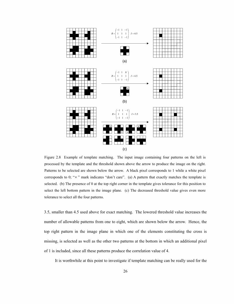
26
3.5, smaller than 4.5 used above for exact matching. The lowered threshold value increases the
number of allowable patterns from one to eight, which are shown below the arrow. Hence, the
top right pattern in the image plane in which one of the elements constituting the cross is
missing, is selected as well as the other two patterns at the bottom in which an additional pixel
of 1 is included, since all these patterns produce the correlation value of 4.
It is worthwhile at this point to investigate if template matching can be really used for the
5.4111
111111
=
−−
−−= IR
5.4111
111011
=
−−
−= IR
5.3111
111111
=
−−
−−= IR
(a)
(b)
(c) Figure 2.8 Example of template matching. The input image containing four patterns on the left is
processed by the template and the threshold shown above the arrow to produce the image on the right.
Patterns to be selected are shown below the arrow. A black pixel corresponds to 1 while a white pixel
corresponds to 0; “× ” mark indicates “don’t care”. (a) A pattern that exactly matches the template is
selected. (b) The presence of 0 at the top right corner in the template gives tolerance for this position to
select the left bottom pattern in the image plane. (c) The decreased threshold value gives even more
tolerance to select all the four patterns.
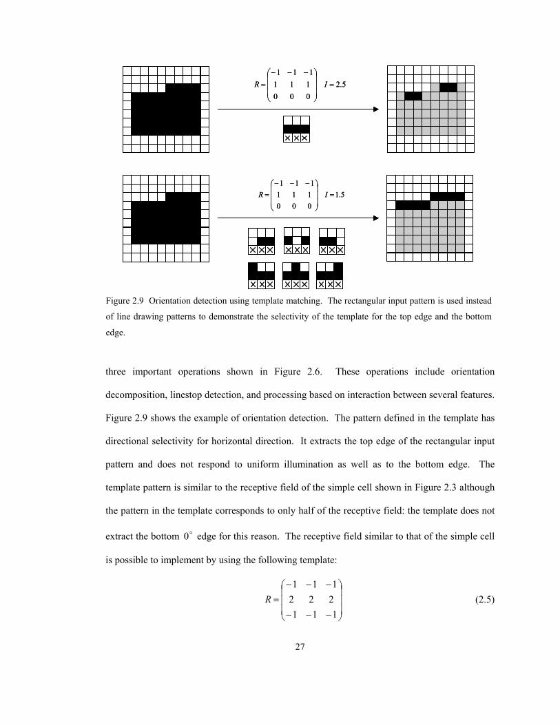
27
three important operations shown in Figure 2.6. These operations include orientation
decomposition, linestop detection, and processing based on interaction between several features.
Figure 2.9 shows the example of orientation detection. The pattern defined in the template has
directional selectivity for horizontal direction. It extracts the top edge of the rectangular input
pattern and does not respond to uniform illumination as well as to the bottom edge. The
template pattern is similar to the receptive field of the simple cell shown in Figure 2.3 although
the pattern in the template corresponds to only half of the receptive field: the template does not
extract the bottom o0 edge for this reason. The receptive field similar to that of the simple cell
is possible to implement by using the following template:
−−−
−−−=
111222111
R (2.5)
5.2000111111
=
−−−= IR
5.1000111111
=
−−−= IR
5.2000111111
=
−−−= IR
5.1000111111
=
−−−= IR
Figure 2.9 Orientation detection using template matching. The rectangular input pattern is used instead
of line drawing patterns to demonstrate the selectivity of the template for the top edge and the bottom
edge.

28
if the value of 2 is allowed for elements in the template. For dealing with the four orientations,
it is necessary to allow the value of 2 for all elements in the template, which complicates the
template construction in hardware. Therefore, the template corresponding to the top edge and
the bottom edge is separately realized. Figure 2.9 also shows the effect of the threshold. All the
points along the top edge are not selected with a threshold of 2.5 while all these points are
selected with a threshold of 1.5.
The second operation important for the feature detection is the detection of linestops.
Figure 2.10 shows the application of template matching for this purpose. By using the template
for which the value of 2 is allowed at the center with the threshold value of 0.5 enables the
detection of linestops regardless of the orientation of line segments. The template selects pixels
that have only one neighbor in either horizontal or vertical direction as linestops. Pixels located
in the middle of the line, which has two neighbors, are deleted by the negative contribution from
two neighbors. Note that the threshold value of 0.5, which indicates lowered stringency, makes
the implementation of feature detection scheme simple: a set of different templates can be
represented by only one template.
The third operation important for the detection of higher level features is the realization
of excitatory and inhibitory interaction between multiple input images. The three operations
5.0010121
010=
−−−
−= IR
5.0010111
010−=
−−−
−= IR
Figure 2.10 Linestop detection based on template matching. The combination of the template and the
threshold shown above the arrow is equivalent to the combination of the template and the threshold
shown below the arrow.
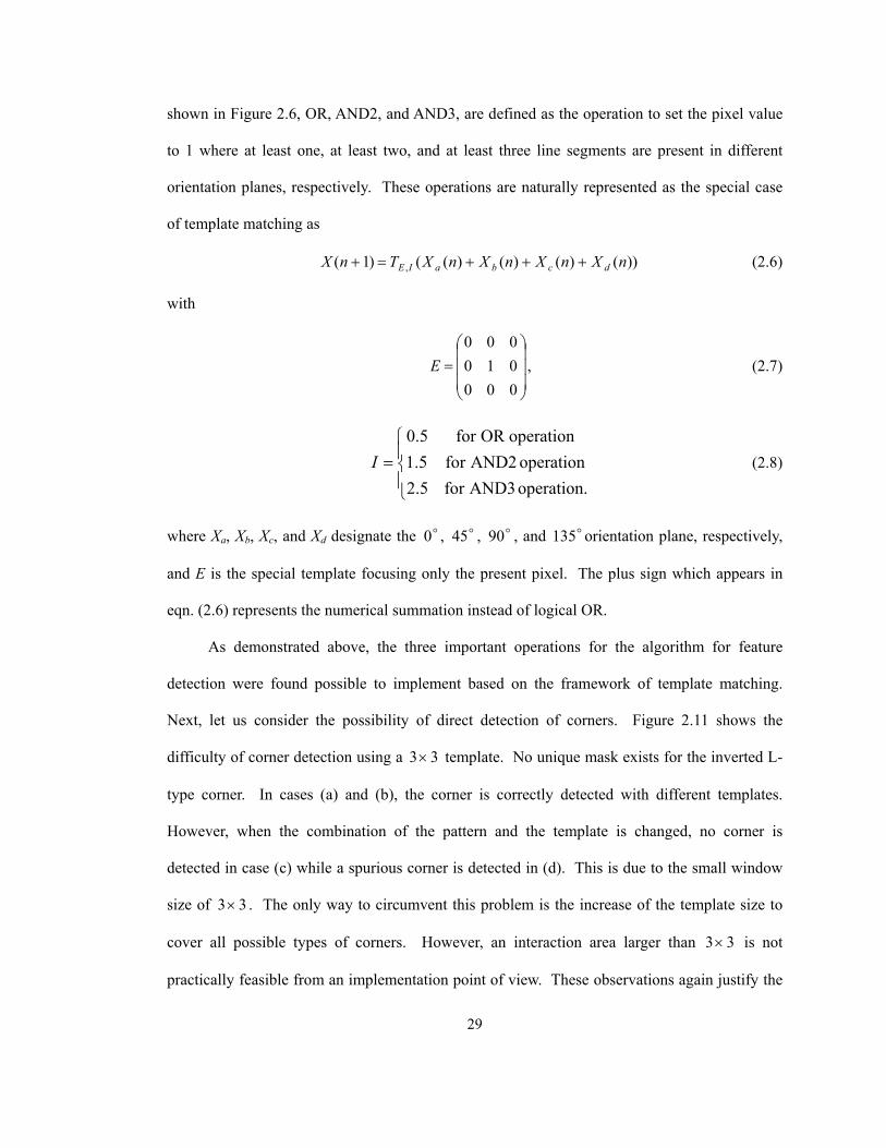
29
shown in Figure 2.6, OR, AND2, and AND3, are defined as the operation to set the pixel value
to 1 where at least one, at least two, and at least three line segments are present in different
orientation planes, respectively. These operations are naturally represented as the special case
of template matching as
))()()()(()1( , nXnXnXnXTnX dcbaIE +++=+ (2.6)
with
=
000010000
E , (2.7)
=
operation. AND3for5.2perationo AND2for5.1
operation ORfor5.0I (2.8)
where Xa, Xb, Xc, and Xd designate the o0 , o45 , o90 , and o135 orientation plane, respectively,
and E is the special template focusing only the present pixel. The plus sign which appears in
eqn. (2.6) represents the numerical summation instead of logical OR.
As demonstrated above, the three important operations for the algorithm for feature
detection were found possible to implement based on the framework of template matching.
Next, let us consider the possibility of direct detection of corners. Figure 2.11 shows the
difficulty of corner detection using a 33× template. No unique mask exists for the inverted L-
type corner. In cases (a) and (b), the corner is correctly detected with different templates.
However, when the combination of the pattern and the template is changed, no corner is
detected in case (c) while a spurious corner is detected in (d). This is due to the small window
size of 33× . The only way to circumvent this problem is the increase of the template size to
cover all possible types of corners. However, an interaction area larger than 33× is not
practically feasible from an implementation point of view. These observations again justify the
30
approach of the proposed algorithm where the corner is defined as the intersection of linestops
of lines in different orientations.
Before going into the detail of the algorithm, it is useful to mention the relationship
between the template matching and the convolution operation. Eqn. (2.1) can be rewritten as
∑ ∑−= −=
−−=+1
1
1
1, ))(()1(
l mlmmjliij knxfnx (2.9)
where
mlml rk −−= . (2.10)
Eqn. (2.9) represents the convolution operation for image X(n) with the kernel K, which is the
flipped version of the template R in both horizontal and vertical directions. In this
representation, the kernel K is better understood as an operator, or a filtering element, rather
than as a template: the original image X(n) is processed with the operator K. The operator
5.2111111
111=
−−−−
−−= IR 5.2
111111111
=
−−−
−−−= IR
5.2111111
111=
−−−−
−−= IR5.2
111111111
=
−−−
−−−= IR
(a) (b)
(c) (d) Figure 2.11 Schematic explaining the difficulty of corner detection using a 33 × template. In (a) and
(b), the corner is correctly detected with different templates. When the combination of the pattern and
the template is changed as shown in (c) and (d), no corner is detected in (c) and misclassification occurs
in (d).

31
exicites neighborhood pixels where element klm is positive while it inhibits neighborhood pixels
where element klm is negative. It should be noted that the template matching and the
convolution is the two sides of the same coin, stating the same thing from different perspectives.
However, the different viewpoints are sometimes useful as described in the next subsection.
2.5.2 Relationship with other image processing methods
There are several image processing methods that have a close relationship with the template
matching scheme. These methods include mathematical morphology and discrete time cellular
neural network. A brief survey of these two methods is given below to provide a unified and clear
viewpoint for understanding template matching scheme.
Mathematical morphology performs image processing operations based on set theory
[22]. Morphological operations nonlinearly transform an image by locally modifying the
geometric features in an image using the set relationship between the input image and the so-
called “structuring element”. Before describing the morphological operation, some basic
definitions on the set operations are described below. Let A and B be sets in Z2 with
components ),( 21 aaa = and ),( 21 bbb = , respectively2.
The translation of A by ),( 21 xxx = , denoted (A)x, is defined as
}for,{)( AaxaccA x ∈+== . (2.11)
The reflection of B, denoted B)
, is defined as
}for,{ BbbxxB ∈−==)
. (2.12)
The complement of set A, denoted cA is
}{ AxxAc ∉= . (2.13)
The union of two sets A and B, denoted BAU is defined as
2Each element of a set is a 2-D vector which represents the row and the column position of a black (by
convention) pixel in the image.

32
}or{ BxAxxBA ∈∈=U . (2.14)
The intersection of two sets A and B, denoted BAI , is defined as
}and{ BxAxxBA ∈∈=I . (2.15)
Finally, the difference of two sets A and B, denoted BA − , is defined as
cBABxAxxBA I=∉∈=− },{ . (2.16)
Using the above notation, dilation of set A by the structuring element B, denoted BA ⊕ ,
is defined as
}.)ˆ({ ∅≠=⊕ ABxBA x I (2.17)
where ∅ is the empty set. The dilation of A is the set of all x displacements such that B)
and A
overlap by at least one nonzero element. Another definition of dilation can be written as
UUAa
aBb
b BABA∈∈
==⊕ )()( , (2.18)
which is exactly the same as the Minkowski addition of two sets A and B. The dilated image is
obtained as the union of variations of set A translated with different quantities, which are
defined by the structuring element B, or as the union of variations of set B translated with
different quantities, which are defined by A.
Erosion can be defined almost in the same manner as dilation. Erosion of A by B,
denoted BAo− , is defined as
})({ ABxBA x ⊆=−o . (2.19)
This formulation shows that a given pixel in the original image is kept in the eroded image if the
structuring element translated to that pixel is fully contained within the set A. This
representation is equivalent to the following formula3:
3 If –b is replaced with b, this expression becomes identical to the Minkowski subtraction of two sets.
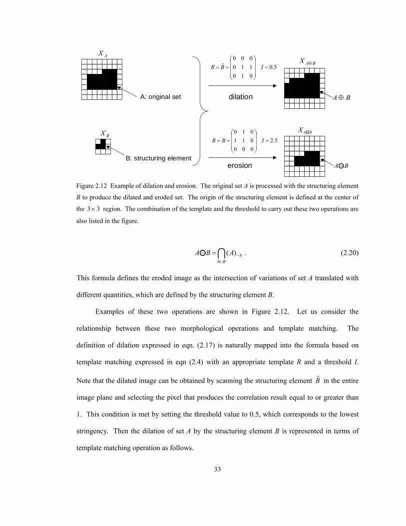
33
IoBb
bABA∈
−=− )( . (2.20)
This formula defines the eroded image as the intersection of variations of set A translated with
different quantities, which are defined by the structuring element B.
Examples of these two operations are shown in Figure 2.12. Let us consider the
relationship between these two morphological operations and template matching. The
definition of dilation expressed in eqn. (2.17) is naturally mapped into the formula based on
template matching expressed in eqn (2.4) with an appropriate template R and a threshold I.
Note that the dilated image can be obtained by scanning the structuring element B̂ in the entire
image plane and selecting the pixel that produces the correlation result equal to or greater than
1. This condition is met by setting the threshold value to 0.5, which corresponds to the lowest
stringency. Then the dilation of set A by the structuring element B is represented in terms of
template matching operation as follows.
5.2000011010
=
== IBR
5.0010110000
ˆ =
== IBR
A: original set
erosion
dilation BA ⊕
B: structuring element BAo−
BAo−X
BAX ⊕
AX
BX
Figure 2.12 Example of dilation and erosion. The original set A is processed with the structuring element
B to produce the dilated and eroded set. The origin of the structuring element is defined at the center of
the 33 × region. The combination of the template and the threshold to carry out these two operations are
also listed in the figure.
34
)(5.0,ˆ AXBA XTXB
=⊕ (2.21)
where XA represents the binary image in which the pixel value is 1 only inside set A, i.e.,
∈∈
=,),(0
),(1),( cA Aji
AjijiX (2.22)
and BAB XX ⊕andˆ are defined almost in the same way. For simlicity reasons, throughout the
formulation in the thesis, set A and image XA are used interchangeably. By this definition,
expressions like “image A” or BA XX ⊕ should be interpreted as “image XA” or BA ⊕ ,
respectively.
It is also suggestive to think about the meaning of the second definition of dilation
represented in eqn. (2.18). This definition is better interpreted from the viewpoint of
convolution operation rather than from the point of correlation. This viewpoint considers B an
operator or a kernel rather than a template. Convolution of the original image with the kernel B
produces the superimposed version of all possible displacements of image A, in which
displacements are defined by B. Then by digitizing the convolution result with the threshold
0.5, the union operation in eqn. (2.18) is performed to produce the dilated image BA ⊕ . Note
that the template matching using the reference template B̂ is equivalent to the convolution
using the kernel B as shown in eqns. (2.9) and (2.10).
The erosion operation can be also related to the template matching operation as well as to
the convolution operation. The first definition in eqn. (2.19) indicates that the eroded image can
be obtained by scanning the structuring element B in the entire image A and selecting the pixel
whose 33× neighbors completely contain B. This condition is met by imposing the maximum
stringency, i.e., by setting the threshold to 2.5 in the example shown in Figure 2.12. Then the
erosion of image A by the structuring element B is rewritten by the following template matching
operation:
35
)(5.2, ATBA B=−o . (2.23)
Like in the case of dilation, the interpretation by convolution is more closely associated
with the definition based on the modified Minkowski subtraction represented in eqn. (2.20).
Convolution of the original image with the kernel B̂ , equivalent to the template matching with
template B, produces the superimposed version of all possible displacements of image A, in
which displacements are defined by B̂ . Then by thresholding the convolution result with the
value 2.5, the intersection operation in eqn. (2.20) is performed to produce the resultant image
AΘB.
The dilation and erosion operations form the basis of the morphological operations.
These two operations do not need 1− in the template, indicating that the template matching is
not performed with the maximum stringency. The combined use of these two operations leads
to opening and closing operations, which are very useful for image filtering applications. The
operation corresponding to the template matching in the strict sense using all the neighborhood
pixels is called Hit-or-Miss transform. It is interesting that the computation based on the set
theory can be mapped into the template matching scheme. The bridge between these two
different methods lies in the thresholding operation, which introduces nonlinearlity.
The other category of image processing method that has some similarity to template
matching is the discrete time cellular neural network (DTCNN), which is a discrete time version
of the cellular neural network (CNN). The CNN is a class of information processing paradigms
which is capable of high speed processing in a parallel fashion [23][24]. It is made of a massive
aggregate of regularly spaced analog components, called cells, which communicate with each
other in a specified region. When the region of cell interaction is limited to 33× neighbors, the
dynamics of the CNN is represented as follows:
36
IuByAxdt
dx
l mmjlilm
l mmjlilmij
ij +++−= ∑ ∑∑ ∑−= −=
++−= −=
++
1
1
1
1
1
1
1
1
τ (2.24)
and
|)1||1(|21)( −−+== ijijijij xxxgy (2.25)
where xij is the internal state of the cell, yij is the output of the cell, uij is the external input to the
cell, τ is the time constant, I is the threshold, A is the feedback template, B is the control
template, g is the function which relates xij to yij. Note that g is linear in the region
11 <<− x and either 1 or 1− outside this region. Several interesting parameter sets are
proposed to perform different types of image processing operations including noise removal,
edge and corner detection [24], shadow detection [25], connected component detection [26],
hole filling [27], and thinning [28].
Let us consider the special case where B is 0. In this case, eqn. (2.24) reduces to
IyAxdt
dx
l mmjlilmij
ij ++−= ∑ ∑−= −=
++
1
1
1
1
τ . (2.26)
The above continuous-time domain representation is transformed into the discrete-time version
by replacing the time derivative dtdxij / with ( ) ττ /)()( txtx ijij −+ . Then eqn. (2.26) reduces
to
ItyAtxl m
mjlilmij +=+ ∑ ∑−= −=
++ )()(1
1
1
1
τ . (2.27)
If the function g is further simplified as the hard limit function as shown below
<≥
=,00
01)0;(
xx
xf (2.28)
The update rule for the discrete-time version of CNN (DTCNN) is represented as follows
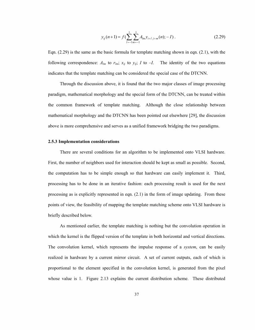
37
));(()1(1
1
1
1
InyAfnyl m
mjlilmij −=+ ∑ ∑−= −=
++ . (2.29)
Eqn. (2.29) is the same as the basic formula for template matching shown in eqn. (2.1), with the
following correspondence: Alm to rlm; xij to yij; I to –I. The identity of the two equations
indicates that the template matching can be considered the special case of the DTCNN.
Through the discussion above, it is found that the two major classes of image processing
paradigm, mathematical morphology and the special form of the DTCNN, can be treated within
the common framework of template matching. Although the close relationship between
mathematical morphology and the DTCNN has been pointed out elsewhere [29], the discussion
above is more comprehensive and serves as a unified framework bridging the two paradigms.
2.5.3 Implementation considerations
There are several conditions for an algorithm to be implemented onto VLSI hardware.
First, the number of neighbors used for interaction should be kept as small as possible. Second,
the computation has to be simple enough so that hardware can easily implement it. Third,
processing has to be done in an iterative fashion: each processing result is used for the next
processing as is explicitly represented in eqn. (2.1) in the form of image updating. From these
points of view, the feasibility of mapping the template matching scheme onto VLSI hardware is
briefly described below.
As mentioned earlier, the template matching is nothing but the convolution operation in
which the kernel is the flipped version of the template in both horizontal and vertical directions.
The convolution kernel, which represents the impulse response of a system, can be easily
realized in hardware by a current mirror circuit. A set of current outputs, each of which is
proportional to the element specified in the convolution kernel, is generated from the pixel
whose value is 1. Figure 2.13 explains the current distribution scheme. These distributed
38
currents are summed at each pixel to produce the convolution result, which are then digitized by
a threshold current to generate a binary output voltage.
The first requirement for hardware mapping is satisfied if currents are distributed only to
its 33× neighbors. The second requirement concerning the simplicity of computation is
satisfied by the use of only three current levels, which are refI , refI− , and 0 except the center
where the value of refI2 is also allowed. These three values can be generated by appropriately
turning on or turning off current sources. Iterative operation, which is the third requirement, is
easily realized in hardware by implementing a memory for each pixel. From these observations,
it is concluded that the employment of template matching scheme is suitable for the realization
of the feature detection algorithm from the implementation point of view. The detail of
implementation is described in Chapter 3.
IN INE
IE
ISEISISW
IW
INW
mllm
ESSWS
ECW
NWNNW
rk
kIIIII
III
kkkkkkkkk
K
−−
−
−
−−−−
=
=
=
110111
100010
110111
Figure 2.13 Implementation of a convolution kernel. The convolution kernel is realized by the current
distribution from the pixel whose value is 1. Each current amount takes one of the three values, refI , 0,
refI− where refI is the amount of the reference current. Only at the center pixel is allowed to have the
value of refI2 in addition to the above three values.
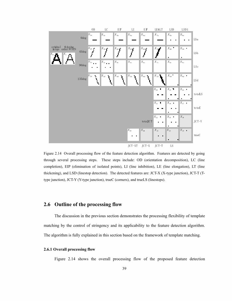
39
2.6 Outline of the processing flow
The discussion in the previous section demonstrates the processing flexibility of template
matching by the control of stringency and its applicability to the feature detection algorithm.
The algorithm is fully explained in this section based on the framework of template matching.
2.6.1 Overall processing flow
Figure 2.14 shows the overall processing flow of the proposed feature detection
originalim age
thinningorder: W SEN
OD LC EIP LI
JCT-XT
EIP
JCT-X
LE<
JCT-T
LSD
LS
LSD1
LSa
LSb
LSc
LSd
totalLS
totalC
JCT-Y
trueC
totalJC T
0deg
45deg
90deg
135degdX 9
aX 9
bX 9
cX 9
dX 2
aX 2
bX 2
cX 2
dX 3
aX 3
bX 3
cX 3
dX 4
aX 4
bX 4
cX 4
dX 5
aX 5
bX 5
cX 5
dX 6
aX 6
bX 6
cX 6
dX 7
aX 7
bX 7
cX 7
dX 8
aX 8
bX 8
cX 8
10X
1X
11X
12X
13X
14X
15X
16X
17X
18X
19X 20X 21X 22X 23X
0X
Figure 2.14 Overall processing flow of the feature detection algorithm. Features are detected by going
through several processing steps. These steps include: OD (orientation decomposition), LC (line
completion), EIP (elimination of isolated points), LI (line inhibition), LE (line elongation), LT (line
thickening), and LSD (linestop detection). The detected features are: JCT-X (X-type junction), JCT-T (T-
type junction), JCT-Y (Y-type junction), trueC (corners), and trueLS (linestops).

40
algorithm, which basically follows the processing shown in Figure 2.6 with additional steps of
processing. Each image in the figure is marked with Xi for later reference4. The original image
is sequentially processed in an iterative fashion to finally generate the five features shown in the
shaded boxes. These processing steps include: orientation decomposition (OD), line completion
(LC), elimination of isolated points (EIP), line inhibition (LI), line elongation (LE), line
thickening (LT), and linestop detection (LSD, LSD1). Each of the processing steps is described
below in detail.
2.6.2 Thinning
The first processing step is thinning. As mentioned in Figure 2.6, thinning is performed
to normalize the line segment in the input pattern to a single pixel width so that the width of the
line does not affect the feature detection processing. Without this processing, it is impossible to
apply the feature detection algorithm for an input pattern containing thick lines since the extent
of interaction is limited to 33× neighbors.
4 The subscript i can be related to the discrete instant n in eqn. (2.1), but is not necessarily numbered
according to the order of computation.
delete
no change
11A 2
1A
31A 4
1A
Figure 2.15 Algorithm for thinning. A pixel is deleted if its 33 × neighbors match either 1
1A or 21A and
match neither 31A nor 4
1A .

41
The basic principle of thinning is to erode the line segment from both sides as long as the
deletion of pixels does not break the line segment. First of all, the possibility of being able to
delete a pixel is examined for all the pixels. Figure 2.15 shows the examination procedure of
the possibility of being able to erode a line segment by deleting a pixel from the west side. If
the 33× neighbors of the present pixel match either template 11A or 2
1A , indicating the
possibility that the present pixel is just an extra or redundant element to the vertical line, it
becomes a candidate for deletion. It is deleted unless the deletion breaks a horizontal
connection to generate a gap: if the 33× neighbors match either 31A or 4
1A , the deletion of the
pixel causes the break between the pixel on the left column and the pixel on the right column.
This procedure of conditional deletion of a pixel is repeated from the south side, from the east
side, and from the north side, by successively rotating the template to complete one cycle of
erosion. This erosion cycle is repeated as many times as required for the thinning result to reach
a stable state.
The thinning operation from the west side is represented in the framework of set theory as
follows:
)))()(())()((( 0,0,0,0,01 41
41
31
31
21
21
11
11
XTXTXTXTXX IAIAIAIA UU −−= (2.30)
Figure 2.16 Example of thinning (one cycle). The leftmost letter is thinned in the order of west, south,
east, and north (indicated by the arrow) to produced the rightmost letter.

42
or equivalently represented in the framework of template matching as
))))()(())()(((( 0,0,5.0,0,0,5.0,5.0,05.0,1 41
41
31
31
21
21
11
11
XTXTTXTXTTTXTX IAIAEIAIAEEE +−+−= (2.31)
where X0 is the input image plane containing patterns and
−=
−=
−=
−=
011110000
,000110011
,100111000
,000111100
41
31
21
11 AAAA , (2.32)
5.041
31
21
11 ==== IIII . (2.33)
The thinning operation from other sides is represented in the same way by using o90 , o180 ,
and o270 rotations of the above templates. Figure 2.16 shows the process of thinning for letter
“A”.
2.6.3 Orientation decomposition
After a line drawing is thinned to a single pixel width, it is decomposed into line
segments of four orientations. This is performed by locally determining the orientation for each
pixel in the image plane based on its 33× neighborhood. The local orientation of a pixel is
computed as o0 if its 33× neighbors match one of the four template patterns listed in Figure
2.17. The first two templates, 12aA and 2
2aA , are designed to detect o0 orientation even for lines
which consists of a horizontal line segment and additional pixels on either the top side or the
5.2
000111111
12
12
=
−−−=
a
a
I
A
5.2
111111000
22
22
=
−−−=
a
a
I
A
5.2
111111111
32
32
=
−−
−−=
a
a
I
A
5.2
111111111
42
42
=
−−
−−=
a
a
I
A
Figure 2.17 Patterns categorized as o0 with its corresponding template and threshold.

43
bottom side. The other two templates, 32aA and 4
2aA , are designed to deal with special cases in
which the pixel is adjacent to the T-type junction. The pixel is not classified as o0 using the
template 12aA and 2
2aA due to the presence of a vertical line segment on either left or right side.
The formula for updating the image is represented as
)()()()( 1,1,1,1,2 42
42
32
32
22
22
12
12
XTXTXTXTXaaaaaaaa IAIAIAIAa UUU= (2.34)
or
))()()()(( 1,1,1,1,5.0,2 42
42
32
32
22
22
12
12
XTXTXTXTTXaaaaaaaa IAIAIAIAEa +++= (2.35)
where
,111111111
,111
111111
,111
111000
,000111111
42
32
22
12
−−
−−=
−−
−−=
−−−=
−−−= aaaa AAAA (2.36)
5.242
32
22
12 ==== aaaa IIII . (2.37)
The o90 orientation component can be obtained exactly the same way by using the o90
rotations of the templates 42
32
22
12 and,,, aaaa AAAA .
The orientation detection for o45 and o135 is slightly different from the detection for o0
and o90 in terms of stringency. For a pixel to be classified as o45 orientation, its 33×
5.1
111110
100
12
12
=
−−−=
b
b
I
A
5.1
001011111
22
22
=
−
−−=
b
b
I
A
Figure 2.18 Patterns categorized as o45 with its corresponding template and threshold.
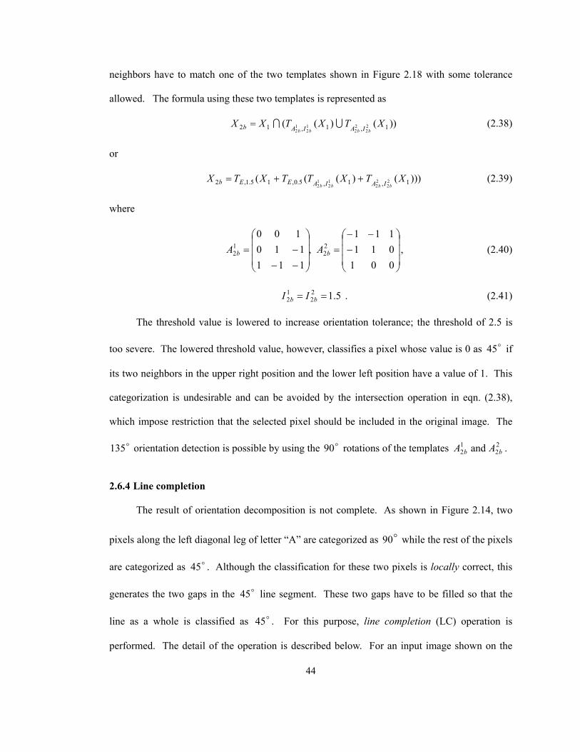
44
neighbors have to match one of the two templates shown in Figure 2.18 with some tolerance
allowed. The formula using these two templates is represented as
))()(( 1,1,12 22
22
12
12
XTXTXXbbbb IAIAb UI= (2.38)
or
)))()((( 1,1,5.0,15.1,2 22
22
12
12
XTXTTXTXbbbb IAIAEEb ++= (2.39)
where
−
−−=
−−−=
001011111
,111110
10022
12 bb AA , (2.40)
5.122
12 == bb II . (2.41)
The threshold value is lowered to increase orientation tolerance; the threshold of 2.5 is
too severe. The lowered threshold value, however, classifies a pixel whose value is 0 as o45 if
its two neighbors in the upper right position and the lower left position have a value of 1. This
categorization is undesirable and can be avoided by the intersection operation in eqn. (2.38),
which impose restriction that the selected pixel should be included in the original image. The
o135 orientation detection is possible by using the o90 rotations of the templates 22
12 and bb AA .
2.6.4 Line completion
The result of orientation decomposition is not complete. As shown in Figure 2.14, two
pixels along the left diagonal leg of letter “A” are categorized as o90 while the rest of the pixels
are categorized as o45 . Although the classification for these two pixels is locally correct, this
generates the two gaps in the o45 line segment. These two gaps have to be filled so that the
line as a whole is classified as o45 . For this purpose, line completion (LC) operation is
performed. The detail of the operation is described below. For an input image shown on the

45
leftmost side in Figure 2.19, which is a typical result of thinning for a slanted cross, the o0
orientation plane is computed as X2a. A gap is generated in the middle of the line, resulting in
two separate line segments from originally one line segment. The purpose of line completion is
to generate X3a, in which the gap is filled to recover the horizontal line. For that purpose, two
steps of intermediate processing are required as shown in the figure. First, each of the broken
line segments is extended to the horizontal direction by using the following operation
)( 2aLEa XTU = (2.42)
where
()() 13
13 , aa IALEa TT = (2.43)
with
5.0,000111000
13
13 =
= aa IA . (2.44)
This elongation operation fills the gap. However the line becomes longer than that in X2a and
the extended portion has to be removed. This is done by the detection of linestops and its
subsequent deletion. The linestops are detected by the following operation which is already
described before in Figure 2.10 as
)(8 UTV LSD= (2.45)
where
X2a V
OD
UX1 X3a
)0( o
Figure 2.19 Procedure of line completion operation in o0 orientation.

46
()()88 ,8 LSDLSD IALSD TT = (2.46)
with
5.0,111121111
88 =
−−−−−−−−
= LSDLSD IA . (2.47)
The image of a completed or recovered line is then computed as a set of pixels that belong to U
and do not belong to V. The above procedure is represented as
( ) ( )( ))()( 2825.0,5.0,3 aLEaLSDaLEaEEa XTTXTTVUTX −=−= . (2.48)
The line completion procedure described above is very similar to closing operation
frequently used in mathematical morphology. The closing of set A by structuring element B,
denoted BA • , is defined as
BBABA o−⊕=• )( (2.49)
which is simply the dilation of A by B, followed by the erosion of the result by B. Closing is
used to fill gaps in the contour as well as to fuse narrow breaks and long thin gulfs. This
morphological operation can be implemented in the framework of template matching since both
dilation and erosion can be represented in terms of template matching (eqns. (2.21) and (2.23)).
However, in the present application, closing with structuring element 13aA cannot fill the gap:
the erosion operation breaks the gap that is filled by the first dilation operation. This is because
the gap width is two while the template or the structuring element is limited to 33× . For this
reason, the erosion operation is replaced with the detection of linestops and subsequent deletion
of these linestops from the line segment.
The line completion procedure for o45 orientation is shown in Figure 2.20, where X2b is
the result of orientation decomposition previously shown in Figure 2.14 and has two gaps in the
middle of the diagonal line. A gap filling operation is performed only for detected linestops as
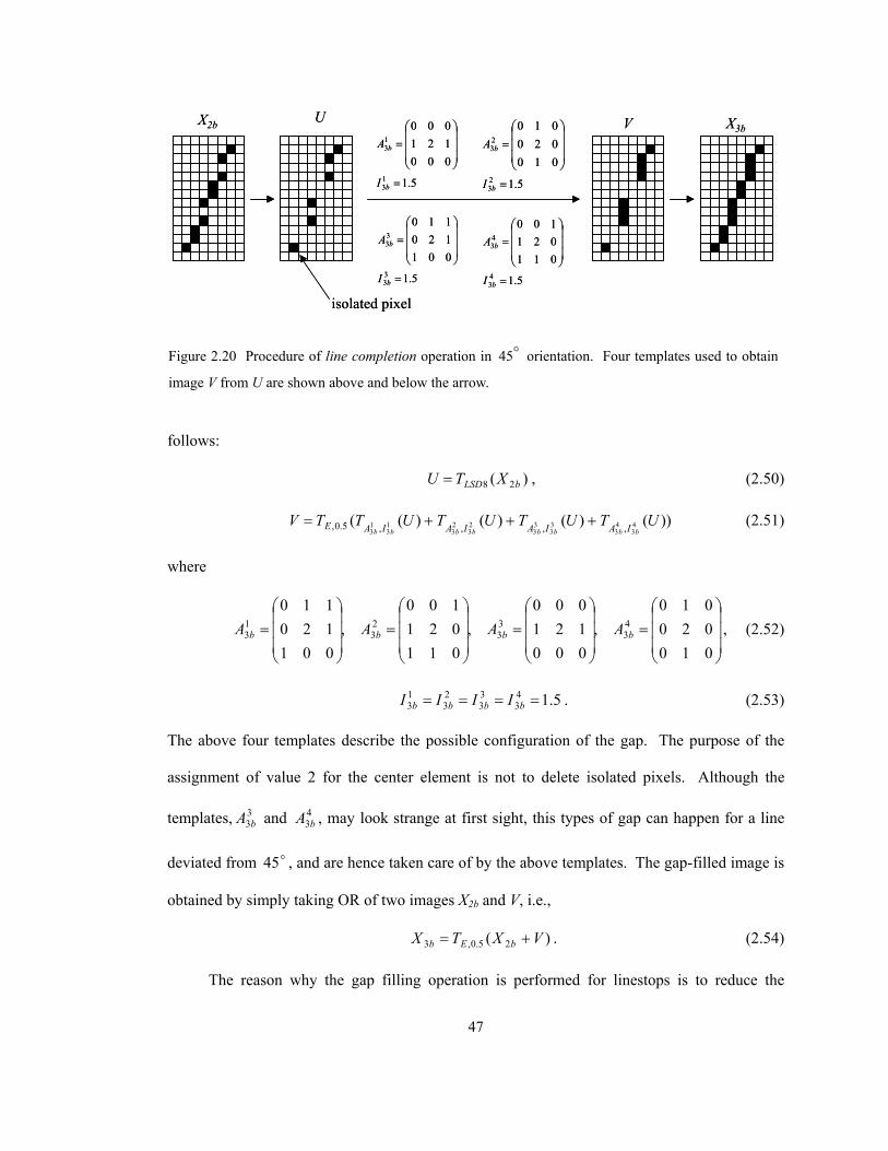
47
follows:
)( 28 bLSD XTU = , (2.50)
))()()()(( 43
43
33
33
23
23
13
13 ,,,,5.0, UTUTUTUTTV
bbbbbbbb IAIAIAIAE +++= (2.51)
where
,010020010
,000121000
,011021100
,001120110
43
33
23
13
=
=
=
= bbbb AAAA (2.52)
5.143
33
23
13 ==== bbbb IIII . (2.53)
The above four templates describe the possible configuration of the gap. The purpose of the
assignment of value 2 for the center element is not to delete isolated pixels. Although the
templates, 33bA and 4
3bA , may look strange at first sight, this types of gap can happen for a line
deviated from o45 , and are hence taken care of by the above templates. The gap-filled image is
obtained by simply taking OR of two images X2b and V, i.e.,
)( 25.0,3 VXTX bEb += . (2.54)
The reason why the gap filling operation is performed for linestops is to reduce the
X2b U V X3b
5.1
010020010
23
23
=
=
b
b
I
A
5.1
001120110
33
33
=
=
b
b
I
A
5.1
011021100
43
43
=
=
b
b
I
A
5.1
000121000
13
13
=
=
b
b
I
A
isolated pixel
X2b U V X3b
5.1
010020010
23
23
=
=
b
b
I
A
5.1
001120110
33
33
=
=
b
b
I
A
5.1
011021100
43
43
=
=
b
b
I
A
5.1
000121000
13
13
=
=
b
b
I
A
isolated pixel
Figure 2.20 Procedure of line completion operation in o45 orientation. Four templates used to obtain
image V from U are shown above and below the arrow.

48
number of templates while allowing some tolerance. If the template matching is performed
directly for the original image, additional points will be detected which results in an
unnecessarily thick line. The line completion for o90 and o135 orientations is possible with the
o90 rotations of the templates for o0 and o45 , respectively, as is the case for orientation
detection. In the following subsections, the processing procedure is explained only for o0 and
o45 ; the procedure for o90 and o135 is obtained by using their o90 rotations unless otherwise
noted.
2.6.5 Elimination of isolated points
The small gaps between line segments generated by orientation decomposition have been
filled by the line completion operation as shown in the orientation plane X3b in Figure 2.14.
Then pixels that are incorrectly classified as other orientation planes (for example X3c) have to
be removed. This is done by elimination of isolated points (EIP) operation as described below.
This operation deletes a single isolated pixel as well as two adjacent pixels since the result of
erroneous orientation detection results in pixel(s) whose length is one or two. A line segment
that consists of three pixels or more survives this operation. In other words, in the proposed
algorithm, the line segment has to have a length of at least three pixels. Note that the EIP
operation should follow the LC operation: otherwise, a set of broken line segments, each of
which can be one or two pixels long, generated immediately after orientation decomposition,
would be eliminated by the EIP operation.
The concept of the EIP operation is opposite to that of the LC operation. Figure 2.21
shows the procedure of the EIP operation in o0 orientation and o45 orientation. First,
linestops are detected in image U and are removed from the original image to generate image V.
This process is represented in the following way.
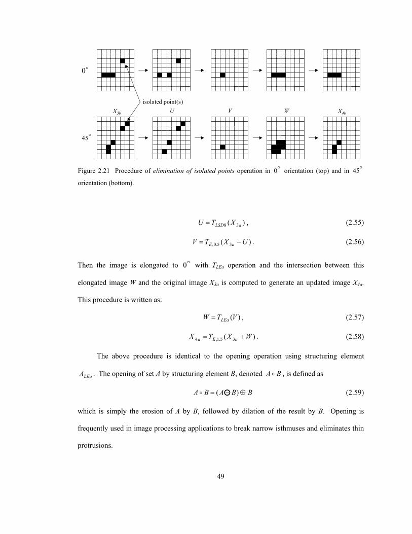
49
)( 38 aLSD XTU = , (2.55)
)( 35.0, UXTV aE −= . (2.56)
Then the image is elongated to o0 with TLEa operation and the intersection between this
elongated image W and the original image X3a is computed to generate an updated image X4a.
This procedure is written as:
)(VTW LEa= , (2.57)
)( 35.1,4 WXTX aEa += . (2.58)
The above procedure is identical to the opening operation using structuring element
LEaA . The opening of set A by structuring element B, denoted BA o , is defined as
BBABA ⊕−= )( oo (2.59)
which is simply the erosion of A by B, followed by dilation of the result by B. Opening is
frequently used in image processing applications to break narrow isthmuses and eliminates thin
protrusions.
U V W
o0
o45
X3b X4b
isolated point(s)
Figure 2.21 Procedure of elimination of isolated points operation in o0 orientation (top) and in o45
orientation (bottom).

50
The procedure for the EIP operation is the same for o45 orientation except the template
used to generate image W from image V. Instead of the o45 rotations of template 14aA , the
following template is used:
=
011111110
14bA . (2.60)
This is because pixels in a line segment of o45 orientation can be mutually connected not only
in an exactly o45 orientation but also in horizontal and vertical directions as the example in
Figure 2.21 shows.
2.6.6 Line inhibition
After EIP operation is performed, errors generated by orientation calculation should have
been fixed. However, there is no guarantee at this point that there is not any pixel of value 1
that is present in multiple orientation planes. Figure 2.22 demonstrates this situation. The line
segment which has an orientation between o45 and o90 is decomposed into two orientation
planes X2b and X2c. These two images are updated by LC and EIP operations to X4b and X4c,
Originalimage
OD LC,EIP LI
X2b
X2c
X4b
X4c
X5b
X5c
o45
o90
Figure 2.22 Procedure of line inhibition operation.
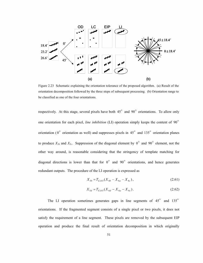
51
respectively. At this stage, several pixels have both o45 and o90 orientations. To allow only
one orientation for each pixel, line inhibition (LI) operation simply keeps the content of o90
orientation ( o0 orientation as well) and suppresses pixels in o45 and o135 orientation planes
to produce X5b and X5c. Suppression of the diagonal element by o0 and o90 element, not the
other way around, is reasonable considering that the stringency of template matching for
diagonal directions is lower than that for o0 and o90 orientations, and hence generates
redundant outputs. The procedure of the LI operation is expressed as
)( 4445.0,5 cabEb XXXTX −−= , (2.61)
)( 4445.0,5 cadEd XXXTX −−= . (2.62)
The LI operation sometimes generates gaps in line segments of o45 and o135
orientations. If the fragmented segment consists of a single pixel or two pixels, it does not
satisfy the requirement of a line segment. These pixels are removed by the subsequent EIP
operation and produce the final result of orientation decomposition in which originally
o4.180 ±
o4.1845 ±
OD LC EIP LI
(a) (b)
o4.18o2.23o6.26
o0
o45
o4.180 ±
o4.1845 ±
o4.180 ±
o4.1845 ±
OD LC EIP LI
(a) (b)
o4.18o2.23o6.26
o0
o45
Figure 2.23 Schematic explaining the orientation tolerance of the proposed algorithm. (a) Result of the
orientation decomposition followed by the three steps of subsequent processing. (b) Orientation range to
be classified as one of the four orientations.

52
generated detection errors should have been corrected. Now it is possible to investigate the
range of orientation that is classified into each of the four orientations. Figure 2.23 (a) shows
the simulation result of the orientation decomposition followed by the above-explained three
steps of processing for three lines of different orientations. The line shown at the top, which has
an orientation of )3/1(tan18.4 1−=o , connecting the origin and the pixel (3,1), is still present in
the o0 orientation plane but is removed from the o45 orientation plane. This indicates that the
original line is categorized as o0 , which is correct since o4.18 is closer to o0 than to o45 .
Note the importance of the LI operation: without this processing, the line is categorized as o0
as well as o45 orientation. This is the maximum orientation deviation from o0 for a line to be
classified as o0 .
On the other hand, the line shown at the bottom, which has an orientation of
)2/1(tan6.62 1−=o , connecting the origin and the pixel (2,1), is classified as o45 . This is the
maximally deviated line to be classified as o45 . In other words, the orientation tolerance is
again oo )6.2645(4.18 −= , which is the same as that for o0 orientation. The line shown in the
middle, whose orientation is )7/3(tan3.32 1−=o , connecting the origin and the pixel (7,3), is
categorized neither as o0 nor as o45 . Figure 2.23 (b) shows the range of orientation that is
categorized as one of the four orientations. The coverage of the orientation is 82 %, which is
reasonably high considering the simplicity of the algorithm for orientation detection.
2.6.7 Line elongation and line thickening
As explained above, the first several steps of processing decomposes an input image into
different orientations. Based on this result, higher level features are detected. Note at this

53
point, no intersection exists between the four orientation planes: no tatalJCT is detected. To
ensure the presence of intersection, line elongation (LE) and line thickening (LT) operations are
performed. For o0 and o90 orientations, only single LE operation is necessary. This operation
has been explained already as part of the LC operation (see eqns. (2.42) and (2.44)), which
simply elongates or extends the line segment using the directional template as shown in Figure
2.24. This operation recovers the original length of the line, which is observed in Figure 2.24
when compared to Figure 2.19. With this operation, some pixels are intentionally allowed to
have multiple orientations to be detected as totalJCT by the intersection operation in the
proposed algorithm. LE operation has another purpose of establishing 4-connectivity5. This
simplifies the process of linestop detection as explained later on. Note that up to this point the
line segment has been treated as a set of pixels that are 8-connected6.
For o45 orientation, the simple line elongation using the following template:
5.0,001010100
27
27 =
= bb IA (2.63)
does not automatically generate a line in which pixels are 4-connected. Another possible
problem is that the simple intersection operation may not produce any pixel of value 1 for letter
“X”, depending on how it is decomposed into line segments of o45 and o135 orientations.
Therefore, the LT operation needs to be performed for an image extended in o45 orientation.
The overall operation is defined as
))(( 6,,7 17
17
27
27
bIAIAb XTTXbbbb
= (2.64)
where 5 Two pixels are said to be 4-connected or to have 4-connectivity if they are adjacent in either horizontal
or vertical direction. 6 Two pixels are said to be 8-connected or to have 8-connectivity if they are adjacent to each other in one
of the four orientations (horizontal, vertical, right diagonal, left diagonal).

54
5.1,000021011
17
17 =
−= bb IA . (2.65)
The above template finds a pixel that has a pixel of value 1 at its upper position and its left
position and a pixel of value 0 at its upper left position, and set the pixel value to 1. This
operation thickens the line segment. The purpose of the assignment of value 2 for the center
element is to avoid deletion of pixels whose 33× neighbors do not match the template pattern.
2.6.8 Linestop detection
For the line segment for which 4-connectivity is established by the LE and the LT
operation, the linestop detection (LSD) operation with a simplified template is performed. The
LSD operation is expressed as
),,,()( 748 dcbapXTX pLSDp == (2.66)
where
()()44 ,4 LSDLSD IALSD TT = (2.67)
with
LE
LE LTo45
o0
X6a X7a
X6b X7b
Figure 2.24 Line elongation operation and line thickening operation explained for o0 and o45
orientations.

55
5.0,010121
010
44 =
−−−
−= LSDLSD IA . (2.68)
With this operation, pixels that are not linestops are removed since they have two neighbors in
horizontal or vertical directions. Note that this template can be commonly used for the four
orientations.
2.6.9 Detection of higher level features
Using the thickened oriented line segment and linestops, detection of higher level features
is possible. The first step for junction detection is to find the pixel where at least two
orientations are designated, which is represented as
)(X 77775.1,10 dcbaE XXXXT +++= . (2.69)
At this stage, however, one junction may consist of a set of mutually connected pixels. Then it
is desirable to shrink each junction to a single pixel so that the number of pixels in the image
plane represents the number of junctions. A normal way of shrinking is to prepare several
templates representing possible connections between pixels for removing pixels that are located
at “peripheries”. Iterative execution of this process should finally shrink a set of mutually
connected pixels into a single pixel. Instead of the above method, a simplified approach with
smaller number of templates is employed in the proposed algorithm. The method first expands
a set of mutually connected pixels to a circumscribing rectangle and then shrinks the rectangle
to a single pixel. Generation of the circumscribing rectangle is performed by the following
operation:
))(( 1011 XTTX CirRectCirRect= (2.70)
where
())))(((() 111
111
211
211
311
311
411
411 ,,,, IAIAIAIACirRect TTTTT = (2.71)

56
with
,000120010
,010120000
,010021000
,000021010
411
311
211
111
=
=
=
= AAAA (2.72)
5.1411
311
211
111 ==== IIII . (2.73)
In other words, X11 is obtained by applying two cycles of rectangular expansion operation,
which consists of a series of template matching using 411
311
211
111 and,,, AAAA . The maximum
number of the rectangualr expansion operation required to obtain a circumscribing rectangle is
the number of pixels forming a longer edge of the rectangle minus one. After the
circumscribing rectangle is formed, further application of the rectangular expansion operation
does not modify the shape any more. The process of rectangular expansion is shown at the top
row in Figure 2.25. Since the size of the circumscribing rectangle is 33× , execution of the
rectangular expansion operation twice generates a circumscribing rectangle.
The shrinking operation is performed for the circumscribing rectangle obtained. The
procedure is represented as
)( 1112 XTXX EdgeRemtotalJCT == (2.74)
where
())))(((() 112
112
212
212
312
312
412
412 ,,,, IAIAIAIAEdgeRem TTTTT = (2.75)
with
,
000121000
,000121
000,
010020010
,010020010
412
312
212
112
−=
−=
−=
−= AAAA
(2.76)
5.1412
312
212
112 ==== IIII . (2.77)
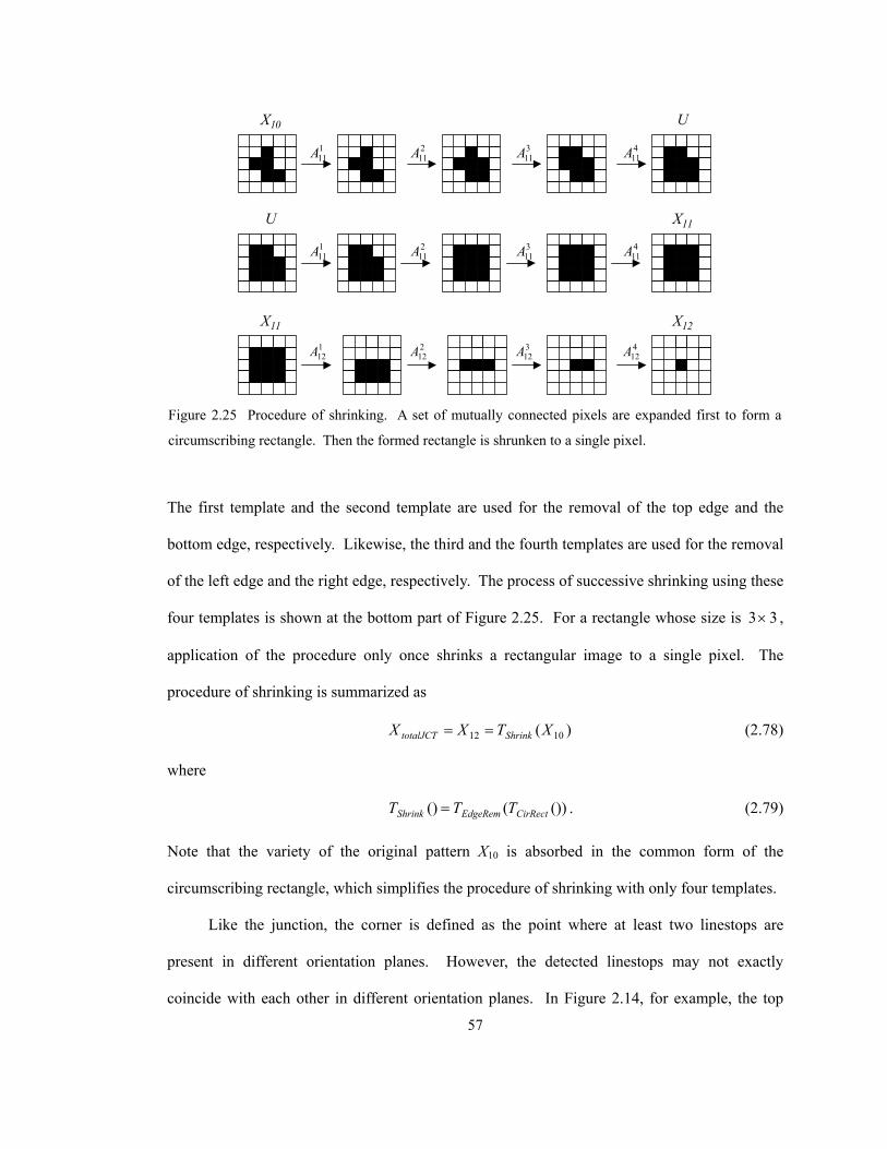
57
The first template and the second template are used for the removal of the top edge and the
bottom edge, respectively. Likewise, the third and the fourth templates are used for the removal
of the left edge and the right edge, respectively. The process of successive shrinking using these
four templates is shown at the bottom part of Figure 2.25. For a rectangle whose size is 33× ,
application of the procedure only once shrinks a rectangular image to a single pixel. The
procedure of shrinking is summarized as
)( 1012 XTXX ShrinktotalJCT == (2.78)
where
())(() CirRectEdgeRemShrink TTT = . (2.79)
Note that the variety of the original pattern X10 is absorbed in the common form of the
circumscribing rectangle, which simplifies the procedure of shrinking with only four templates.
Like the junction, the corner is defined as the point where at least two linestops are
present in different orientation planes. However, the detected linestops may not exactly
coincide with each other in different orientation planes. In Figure 2.14, for example, the top
X10 U
U X11
111A 2
11A 311A 4
11A
111A 2
11A 311A 4
11A
X11 X12
112A 2
12A 312A 4
12A
Figure 2.25 Procedure of shrinking. A set of mutually connected pixels are expanded first to form a
circumscribing rectangle. Then the formed rectangle is shrunken to a single pixel.

58
corner of letter “A” cannot be detected since the linestop at the upper end of the o45 line
segment and the linestop at the upper end of the o135 line segment are not located at the same
pixel position. Therefore, the position of the linestop should be adjusted. For this purpose, the
following processing is performed first:
)(X 1088885.0,13 XXXXXT dcbaE ++++= . (2.80)
In contrast to eqn. (2.69), which corresponds to AND2 operation for four images, eqn. (2.80) is
obtained by OR operation for the same set of images plus an additional image X10. For the
obtained image, the shrinking procedure consisting of rectangular expansion and the subsequent
edge removal is carried out. The procedure is slightly more involved than the procedure
described before to obtain X12. The shrinking operation is represented as
)))((( 1315 XTTTX ShrinkConnectShrink= (2.81)
which is equivalent to
)))((( 1314 XTTTX ShrinkConnectCirRect= , (2.82)
)( 1415 XTX EdgeRem= (2.83)
where
)()))(((() 114
114
214
214
814
814 ,,, LL IAIAIAConnect TTTT = (2.84)
with
,100020001
,100021010
,010120001
,001020100
,010021100
,001120010
,010020010
,000121000
814
714
614
514
414
314
214
114
=
=
=
=
=
=
=
=
AAA
AAA
AA
(2.85)

59
5.1814
714
614
514
414
314
214
114 ======== IIIIIIII . (2.86)
Except for the first shrinking operation, the meaning of which may not be immediately
clear and hence explained later, the basic idea of TConnect followed by TCirRect is to form an
circumscribing rectangle for a set of pixels, for which a gap of one pixel is allowed between
pixels. To be more specific, TConnect connects two pixels that match the template shown above,
and then forms a circumscribing rectangle. This process is shown in the top row in Figure 2.26.
The rational of this operation is that two pixels detected as linestops, each of which is separated
from the other by one pixel gap, is derived from one pixel. In this example, TShrink operation
prior to TConnect operation does not have any effect. Without this operation, however, the four
pixels shown in the bottom row in Figure 2.26, two of which are mutually connected, are
merged to produce a big rectangle in X14, which leads to a single pixel in X15 after the final edge
removal operation. With TShrink operation, generation of a big rectangle containing initial four
pixels is avoided, which results in two isolated pixels in X15.
The above-explained operation defines the new position of the linestop for a set of line
segments in different orientation planes. The position of each linestop in different orientation
planes is adjusted to the newly defined position:
),,,())(( 88155.1,9 dcbapXTXTX pExpEp =+= (2.87)
where
()()88 ,8 ExpExp IAExp TT = (2.88)
with
5.0,111111111
88 =
= ExpExp IA . (2.89)
Using linestops with their position adjusted, the following three images are computed:
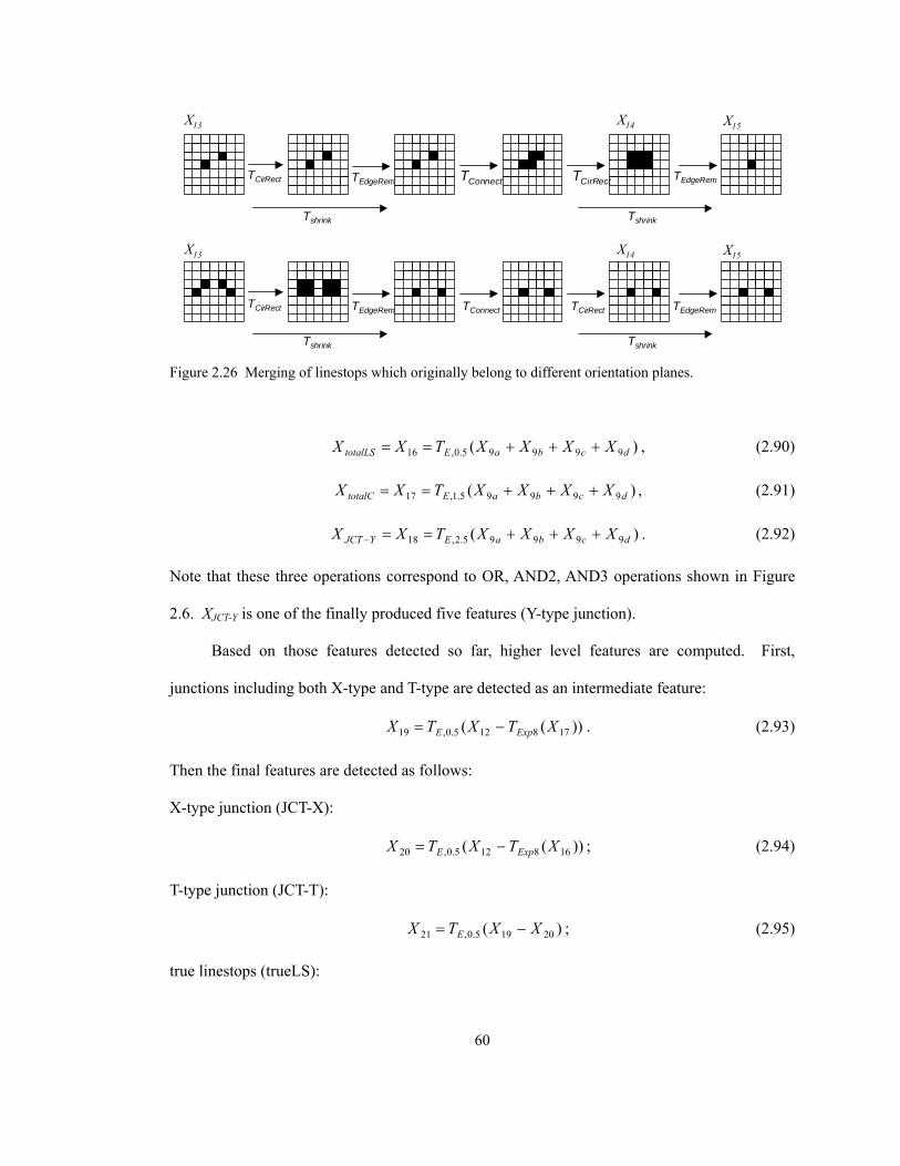
60
)( 99995.0,16 dcbaEtotalLS XXXXTXX +++== , (2.90)
)( 99995.1,17 dcbaEtotalC XXXXTXX +++== , (2.91)
)( 99995.2,18 dcbaEYJCT XXXXTXX +++==− . (2.92)
Note that these three operations correspond to OR, AND2, AND3 operations shown in Figure
2.6. XJCT-Y is one of the finally produced five features (Y-type junction).
Based on those features detected so far, higher level features are computed. First,
junctions including both X-type and T-type are detected as an intermediate feature:
))(( 178125.0,19 XTXTX ExpE −= . (2.93)
Then the final features are detected as follows:
X-type junction (JCT-X):
))(( 168125.0,20 XTXTX ExpE −= ; (2.94)
T-type junction (JCT-T):
)( 20195.0,21 XXTX E −= ; (2.95)
true linestops (trueLS):
TCirRect TEdgeRem
Tshrink
TConnect
TConnect
TCirRect
TCirRect
TEdgeRem
Tshrink
Tshrink Tshrink
TEdgeRem
X13 X14 X15
X13 X14 X15
TCirRect TEdgeRem
Figure 2.26 Merging of linestops which originally belong to different orientation planes.

61
)))(( 17128165.0,22 XXTXTX ExpE −−= ; (2.96)
true corners (trueC):
)( 18175.0,23 XXTX E −= . (2.97)
These relationships can be represented in a more understandable way as:
))(( 85.0, totalCExptotaJCTEXTJCT XTXTX −=− , (2.98)
)(( 85.0, totalLSExptotalJCTEXJXT XTXTX −=− , (2.99)
)(5.0, XJCTXTJCTETJCT XXTX −−− −= , (2.100)
))(( 85.0, totalCtotalJCTExptotalLSEtrueLS XXTXTX −−= , (2.101)
)(5.0, YJCTtotalCEtrueC XXTX −−= . (2.102)
These formulas directly describe the relationship between several features shown in Figure 2.6
and Figure 2.7. The use of TExp8 is to compensate possible mis-alignment of the linestop
position between four orientation planes. The only expression which is not represented in
Figure 2.6 is the inhibition of XtotalLS by XtotalC to derive XtrueLS. (eqn. (2.101)). This should be
unnecessary since XtotalC is a subset of XtotalJCT. There are cases, however, in which the corner is
not detected in XtotalJCT as the intersection of two line segments in different orientations but is
detected in XtotalC as the intersection of two linestops in different orientation planes as a result of
the alignment of linestop position.
2.6.10 Key points of the algorithm
The processing flow for the detection of important image features has been described in
detail in this section. The processing flow consists of thinning, orientation decomposition,
linestop detection, and further processing based on interaction between images of line segments
and linestops in different orientation planes. The two key points of the processing flow are
summarized below.

62
In the error correction stage after orientation decomposition, the minimum length of the
line segment is defined as three pixels: line segments that are one or two pixels long are
removed (EIP operation). Likewise, the gap between two line segments has to be one pixel or
two pixels long so that they are considered a candidate to be filled to recover the originally one
line segment (LC and LE operation). Another important operation in the error correction stage
is the line inhibition operation, which assigns only one orientation for one pixel and
consequently produces the same orientation range ( o4.18± ) for all the four orientations. These
additional steps of processing virtually increase the interaction area to its original 33× region
to a larger area, which leads to the increased robustness of the proposed algorithm.
In the stage for the detection of higher level features, the adjustment of the linestop
position is important to absorb the difference in the position of linestops in different orientation
planes. Since prior to this stage, the processing is carried out in each orientation plane
independently of other orientation planes with the only exception of line inhibition operation,
the position of the linestop corresponding to the same corner could be different. Several
linestops in different orientation planes whose mutual distance is one or two pixels, i.e., a
maximum of one pixel gap is allowed, are considered to represent the same corner and hence
merged together to produce a single linestop. Note that this rule does not contradict with the
above-mentioned rule of the minimum line length of three. The LE operation ensures that the
minimum length of the line segment is five, avoiding the merging of two linestops belonging to
the same line. Note also that almost similar idea of compensating the difference in the position
of features in the four orientation planes is realized by the use of TExp8 operation.
2.7 Evaluation of the algorithm
The feature detection algorithm explained in detail in the previous section is applied to

63
printed and handwritten characters as well as simple patterns to evaluate its performance.
2.7.1 Printed characters
Figure 2.27 shows the simulation result for printed characters with the proposed
algorithm. For twenty-six alphabetical characters, the result of thinning is shown below the
corresponding original character; the detected features are superimposed on the thinned
character. The font type is Arial with a 3232 × resolution. The simulation result demonstrates
that the algorithm is able to detect almost all important features in a discriminative fashion.
These features include T-type junctions in letters “E”, “F”, “H” “K”, “P”, “R”, “T”, and X-type
trueLS
JC T-T & trueC
JC T-X
JC T-Y
Figure 2.27 Features detected by the proposed algorithm for alphabetical characters. The center of a
closed rectangle indicates the position of a feature. The shade of the rectangle represents the type of the
feature.
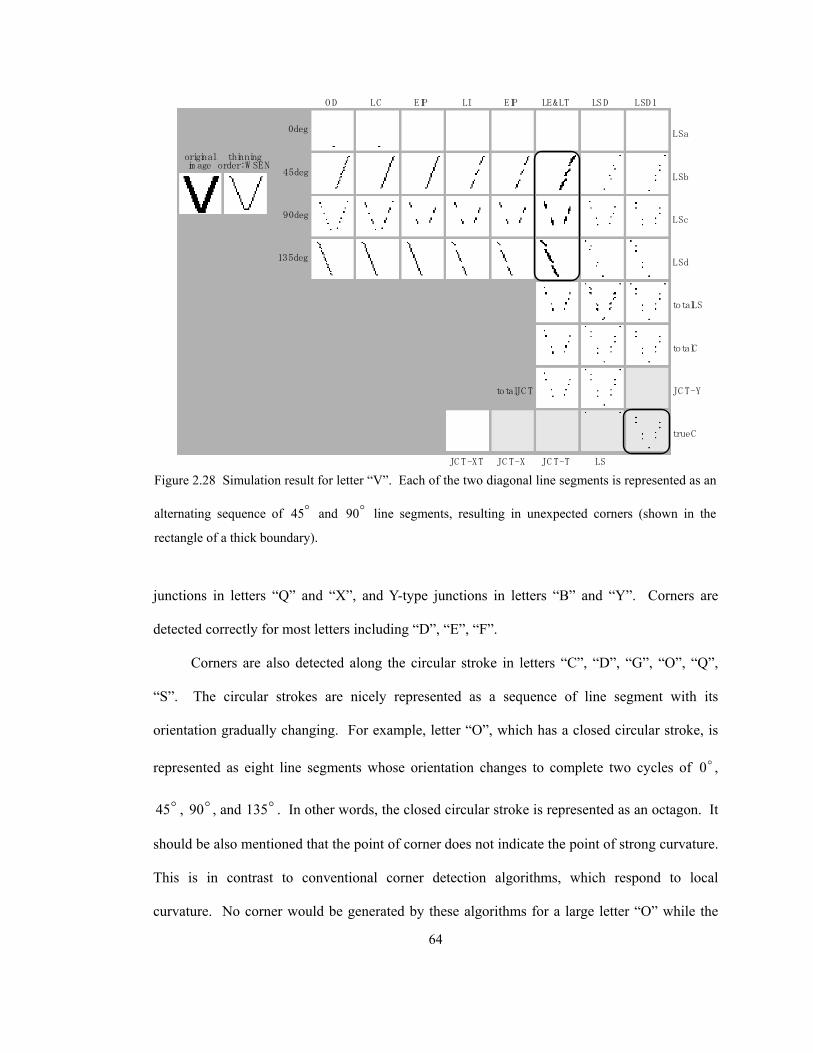
64
junctions in letters “Q” and “X”, and Y-type junctions in letters “B” and “Y”. Corners are
detected correctly for most letters including “D”, “E”, “F”.
Corners are also detected along the circular stroke in letters “C”, “D”, “G”, “O”, “Q”,
“S”. The circular strokes are nicely represented as a sequence of line segment with its
orientation gradually changing. For example, letter “O”, which has a closed circular stroke, is
represented as eight line segments whose orientation changes to complete two cycles of o0 ,
o45 , o90 , and o135 . In other words, the closed circular stroke is represented as an octagon. It
should be also mentioned that the point of corner does not indicate the point of strong curvature.
This is in contrast to conventional corner detection algorithms, which respond to local
curvature. No corner would be generated by these algorithms for a large letter “O” while the
originalim age
thinningorder: W SEN
O D LC EIP LI
JC T-XT
EIP
JC T-X
LE<
JC T-T
LSD
LS
LSD1
LSa
LSb
LSc
LSd
totalLS
totalC
JC T-Y
trueC
totalJC T
0deg
45deg
90deg
135deg
Figure 2.28 Simulation result for letter “V”. Each of the two diagonal line segments is represented as an
alternating sequence of o45 and o90 line segments, resulting in unexpected corners (shown in the
rectangle of a thick boundary).
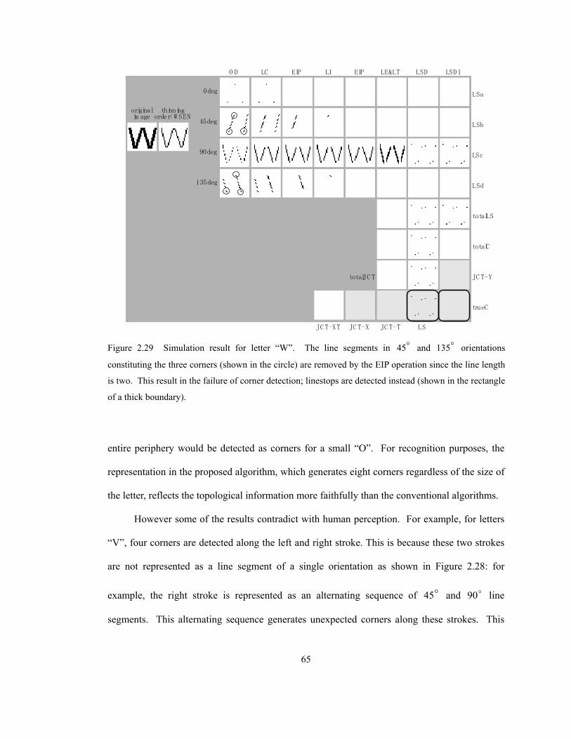
65
entire periphery would be detected as corners for a small “O”. For recognition purposes, the
representation in the proposed algorithm, which generates eight corners regardless of the size of
the letter, reflects the topological information more faithfully than the conventional algorithms.
However some of the results contradict with human perception. For example, for letters
“V”, four corners are detected along the left and right stroke. This is because these two strokes
are not represented as a line segment of a single orientation as shown in Figure 2.28: for
example, the right stroke is represented as an alternating sequence of o45 and o90 line
segments. This alternating sequence generates unexpected corners along these strokes. This
originalim age
thinningorder: W SEN
O D LC EIP LI
JC T-XT
EIP
JC T-X
LE<
JC T-T
LSD
LS
LSD1
LSa
LSb
LSc
LSd
totalLS
totalC
JC T-Y
trueC
totalJC T
0deg
45deg
90deg
135deg
Figure 2.29 Simulation result for letter “W”. The line segments in o45 and o135 orientations
constituting the three corners (shown in the circle) are removed by the EIP operation since the line length
is two. This result in the failure of corner detection; linestops are detected instead (shown in the rectangle
of a thick boundary).

66
type of unexpected corners are also observed in letters “A” and “M”. Although generation of
these unexpected corners for lines in a certain orientation range is not erroneous, it may be
problematic in some cases.
Another problem, which is even more serious, is the failure of corner detection. It is
observed for letter “M” and “W”. The acute angle at the bottom corner in “M” and the three
corners in “W” is not well represented as a sequence of line segments that are allowed to have
only four orientations. As is shown in Figure 2.29, the three corners, one at the top and the two
at the bottom, are decomposed as line segments of o45 and o135 orientations immediately
after orientation decomposition. However, these line segments are removed by the EIP
operation since the length of these line segments is two. As this examples shows, the deletion
of line segments of length two, especially when it happens near corners and junctions,
sometimes results in the failure of detection of these features and results in the detection of
unexpected linestops instead.
Figure 2.30 shows another simulation result performed for the same alphabetical
characters with italic modifications. Overall, most of the features successfully detected in
Figure 2.27 are also detected. This is because with this degree of slanting, line segments that
are originally aligned in either horizontal or vertical direction are still categorized as the same
orientation. Slanting caused favorable effect for letters “M” and “W”, which were previously
difficult to handle as shown in Figure 2.27. Diagonal lines whose original orientation is either
o45 or o135 are categorized as either o0 or o90 in the slanted letter: the slanted “W” is
represented as line segments of o45 and o90 . As a result of this, all the three corners were
correctly detected.

67
However, several patterns causing problems are found by this simulation. T-type
junctions are not correctly detected for letters “K” and “R” since the line segment corresponding
to the stem7 of the T-junction is detected in a shorter form than it should be. This situation is
shown in Figure 2.31 (a) for letter "R". The upper end point of the leg extending toward the
bottom right direction is categorized as o90 while the rest of the line segment is categorized as
o135 orientation. Therefore, the o135 line segment cannot reach the horizontal line segment
(bottom part of the loop) even with the help of the LE operation. For letter "K", no orientation
is assigned to the point indicated in the figure, which makes the o90 line segment shorter to fail
7 The stem indicates the vertical line segment of T. The horizontal line segment is called the bar.
trueLS
JC T-T & trueCJC T-X
JC T-Y
Figure 2.30 Features detected by the proposed algorithm for italic alphabetical characters.

68
to reach the o45 line.
There was another problem found for letters “X” and “Y”. For letter “X”, instead of the
X-type junction at the center of the letter, the T-type junction is detected. For letter “Y”, instead
of the Y-type junction, the T-type junction and the corner are detected. These somewhat
confusing results are associated with the result of thinning as shown in Figure 2.32 for letter
“X”. The thinning operation generated a short vertical line segment between two L-shaped
corners, one is facing upward and the other facing downward. The presence of this vertical line
segment eventually leads to the breaking of the o135 line segment. As a result of this, two T-
type junction are detected as the point of intersection between the o45 line segment and two
o135 line segments. These two T-type junctions are merged to finally produce single T-type
junction. What happens to letter “Y” is somewhat similar. A closer look of the thinning result
indicates the presence of the T-type junction formed between the o45 and the o135 line
segments, and the corner formed by the o45 and the o90 line segments instead of the single Y-
(a) (b)
bar
stem
stem
bar
Point of isolation
Figure 2.31 Pixel point where the stem is separated from the bar of the T-type junction for two letters
“R” and “K”. It is superimposed on the original letter displayed with half-tone color. (a) The local
orientation of this point is computed as o90 . (b) No orientation is assigned to this point.

69
type junction where the above three line segments of different orientations are supposed to
meet.
Figure 2.33 shows the effect of the order of thinning on the detected features. The result
shown in (b) and (d) is obtained by performing the thinning in the order of south, east, north,
and west, while the result in (a) and (c) is obtained in the order of west, south, east, and north.
In (b) and (d), the thinning result maintains the structural shape of the original letter without
generating any redundant line segments as observed in (a) and (c), which resulted in the correct
detection of the features.
originalim age
thinningorder: W SEN
O D LC EIP LI
JC T-XT
EIP
JC T-X
LE<
JC T-T
LSD
LS
LSD1
LSa
LSb
LSc
LSd
totalLS
totalC
JC T-Y
trueC
totalJC T
0deg
45deg
90deg
135deg
Figure 2.32 Simulation results for slanted letter “X”. The vertical line segment (shown in the circle)
generated by thinning leads to the detection of the T-type junction instead of the X-type junction (shown
in the rectangle with a thick boundary).
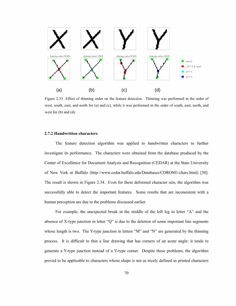
70
2.7.2 Handwritten characters
The feature detection algorithm was applied to handwritten characters to further
investigate its performance. The characters were obtained from the database produced by the
Center of Excellence for Document Analysis and Recognition (CEDAR) at the State University
of New York at Buffalo (http://www.cedar.buffalo.edu/Databases/CDROM1/chars.html) [30].
The result is shown in Figure 2.34. Even for these deformed character sets, the algorithm was
successfully able to detect the important features. Some results that are inconsistent with a
human perception are due to the problems discussed earlier.
For example, the unexpected break in the middle of the left leg in letter “A” and the
absence of X-type junction in letter “Q” is due to the deletion of some important line segments
whose length is two. The Y-type junction in letters “M” and “N” are generated by the thinning
process. It is difficult to thin a line drawing that has corners of an acute angle: it tends to
generate a Y-type junction instead of a V-type corner. Despite these problems, the algorithm
proved to be applicable to characters whose shape is not as nicely defined as printed characters
thinning order: W SEN thinning order: SENW thinning order: W SEN thinning order: SENW
trueLS
JC T-T & trueC
JC T-X
JC T-Y
(a) (b) (c) (d) Figure 2.33 Effect of thinning order on the feature detection. Thinning was performed in the order of
west, south, east, and north for (a) and (c), while it was performed in the order of south, east, north, and
west for (b) and (d).

71
due to some deformation.
2.7.3 Patterns
The algorithm was also applied to several patterns of binary values to test its performance
for more general cases. The simulation was performed without thinning process before
orientation decomposition. The simulation result shown in Figure 2.35 demonstrates that all the
features are successfully detected. For the edge image of a three-dimensional view of the cube,
Y-type junctions and corners are correctly detected. Note that the Y-type junction at the center
bottom would be detected as the T-type junction when the 33× template matching is performed
without considering the neighborhood information. The more global information obtained by
trueLS
JC T-T & trueC
JC T-X
JC T-Y
Figure 2.34 Features detected by the proposed algorithm for handwritten characters. These data were
obtained from the database at http://www.cedar.buffalo.edu/Databases/CDROM1/chars.html [30].
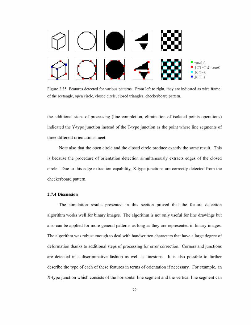
72
the additional steps of processing (line completion, elimination of isolated points operations)
indicated the Y-type junction instead of the T-type junction as the point where line segments of
three different orientations meet.
Note also that the open circle and the closed circle produce exactly the same result. This
is because the procedure of orientation detection simultaneously extracts edges of the closed
circle. Due to this edge extraction capability, X-type junctions are correctly detected from the
checkerboard pattern.
2.7.4 Discussion
The simulation results presented in this section proved that the feature detection
algorithm works well for binary images. The algorithm is not only useful for line drawings but
also can be applied for more general patterns as long as they are represented in binary images.
The algorithm was robust enough to deal with handwritten characters that have a large degree of
deformation thanks to additional steps of processing for error correction. Corners and junctions
are detected in a discriminative fashion as well as linestops. It is also possible to further
describe the type of each of these features in terms of orientation if necessary. For example, an
X-type junction which consists of the horizontal line segment and the vertical line segment can
trueLSJC T -T & trueCJC T -XJC T -Y
Figure 2.35 Features detected for various patterns. From left to right, they are indicated as wire frame
of the rectangle, open circle, closed circle, closed triangles, checkerboard pattern.

73
be discriminated from an X-type junction which consists of two diagonal line segments.
Several problems concerning orientation decomposition were found. The first problem is
the representation of a slanted line. A straight line whose orientation is almost in the middle of
two adjacent orientations may be represented as a sequence of line segments whose orientation
fluctuates between the two orientations, which results in unexpected corners. This
representation contradicts with a human perception, which would like to assign only one
orientation for a single straight line. Therefore, it may be more appropriate to merge these
broken line segments to create a longer line, which is defined as a loosely diagonal line. This is
possible to realize, for example, by newly defining the o45 orientation by including both o0
and o90 line segments in addition to the originally present o45 line segment.
The other problem concerning the orientation decomposition is that there are some pixels
for which no orientation is assigned. Although no orientation is probably the right judge, this
results in the failure of corner detection and failure of junction detection. One of the possible
solutions for this problem is the assignment of the four orientations to those pixels instead of no
orientation assignment. The combined use of this new orientation assignment with the above
mentioned loose representation of diagonal lines is expected to further improve the performance
of the algorithm although detailed investigation needs to be carried out.
It was found that thinning could be problematic especially for line drawings having a
sharp corner: letter “V” could become “Y” after thinning. Another problem is the instability of
the thinning algorithm: the topological information could be different depending on the order of
thinning. Actually there have been a large number of thinning algorithms proposed (see [31] for
review, for example). Each algorithm has its advantages and disadvantages in different aspects.
These aspects include the degree of excessive erosion, generation of spurious branches, and so
on. The most important requirement for the thinning algorithm to be used as preprocessing for

74
the feature detection is being able to preserve the structural shape. Therefore, further
refinement of the present thinning algorithm as well as investigation for other existing
algorithms would be required so that the overall feature detection algorithm works for line
drawing images without being affected by the line width of the pattern.
2.8 Summary
The feature detection algorithm, which is able to detect corners, three types of junctions
(T-type, X-type, Y-type) and linestops of a binary image, is presented in this chapter. The
advantages of the present algorithm over other existing ones is the detection capability of three
types of junctions in a discriminative fashion even though its input is limited to a binary image.
The algorithm is inspired by the biological visual processing, which performs detection
and hierarchical integration of features. The proposed algorithm first decomposes an input
image into four orientations and detects linestops for line segments in each orientation plane.
Corners and junctions are detected as a result of interactions between line segments and
linestops in different orientation planes.
The algorithm is formulated on the basis of template matching which iteratively performs
a 33× neighborhood processing. The degree of matching is determined by comparing the
result of correlation between 33× neighbors and the template to a specified threshold value.
The stringency of template matching can be lowered by decreasing the threshold value, which
results in a smaller number of templates for certain types of processing. The template matching
is suitable for hardware implementation because of its nearest neighborhood interaction. It is
also found that the template matching is closely related to other image processing paradigms,
mathematical morphology and the special form of DTCNN.
To supplement the limitation of a small 33× interaction area, additional steps of
processing are implemented, which includes line completion, elimination of isolated points, and

75
so on. These additional steps of processing virtually increase the area of interaction, which
results in the increased robustness of the algorithm to the deformation of an object. Due to this
mechanism, the features are successfully detected even for handwritten characters with a large
degree of deformation.
2.9 References
[1] F. Attneave, “Some informational aspects of visual perception,” Psychological Review, vol.
61, no. 3, pp. 183-193, 1954.
[2] B. S. Manjunath, C. Shekhar, and R. Chellappa, “A new approach to image feature detection
with applications,” Pattern Recognition, vol. 29, no. 4, pp. 627-640, 1996.
[3] B. A. Wandell, Foundations of Vision, Sinauer Associates, Inc., Sunderland, MA, 1995.
[4] S. W. Kuffler, J. G. Nichols, and A. R. Martin, From Neurons to Brain, Sinauer Associates,
Inc., Sunderland MA, 2nd ed., 1984.
[5] D. H. Hubel and T. N. Wiesel, “Receptive fields, binocular interaction and functional
architecture in the cat’s visual cortex,” Journal of Physiology, vol. 160, pp. 106-154, 1962.
[6] I. Fujita, K. Tanaka, M. Ito, and K. Cheng, “Columns for visual features of objects in
monkey inferotemporal cortex,” Nature, vol. 360, pp. 343-346, 1992.
[7] K. Tanaka, “Neuronal mechanisms of object recognition,” Science, vol. 262, pp. 685-688,
1993.
[8] K. Fukushima and S. Miyake, “Neocognitron: A new algorithm for pattern recognition
tolerant of deformations and shifts in position,” Pattern Recognition, vol. 15, No. 6, pp. 455-
469, 1982.
[9] K. Fukushima and N. Wake, “Handwritten alphanumeric character recognition by the
neocognitron,” IEEE Trans. Neural Networks, vol. 2, no. 3, pp. 355-365, 1991.
[10] S. Knerr, L. Personnaz, and G. Dreyfus, “Handwritten digit recognition by neural networks
76
with single-layer training,” IEEE Trans. Neural Networks, vol. 3, no. 6, pp. 962-968, 1992.
[11] S. Cho, “Neural-network classifiers for recognizing totally unconstrained handwritten
numerals,” IEEE Trans. Neural Networks, vol. 8, no. 1, pp. 43-53, 1997.
[12] J. S. Denker, W. R. Gardner, H. P. Graf, D. Henderson, R. E. Howard, W. Hubbard, L. D.
Jackel, H. S. Baird and I. Guyon, "Neural network recognizer for hand-written zip code digits,"
Advances in Neural Information Processing Systems, (D. Touretzky ed.), vol. 1, Morgan
Kaufman, San Mateo, CA, p. 323-331, 1989.
[13] F. Heitger, L. Rosenthaler, R. V. D. Heydt, E. Peterhans, and O. Kübler, “Simulation of
neural contour mechanisms: from simple to end-stopped cells,” Vision Research, vol. 32, no. 5,
pp. 963-981, 1992.
[14] W. T. Freeman, “Steerable filters and analysis of image structures”, Ph. D. dissertation,
Massachusetts Institute of Technology, Cambridge, MA, 1992.
[15] A. Dobbins, S. W. Zucker, and M. S. Cynader, “Endstopped neurons in the visual cortex as
a substrate for calculating curvature,” Nature, vol. 329, pp. 438-441, 1987.
[16] A. Dobbins, S. W. Zucker, and M. S. Cynader, “Endstopping and curvature,” Vision
Research, vol. 29, no. 10, pp. 1371-1387, 1989.
[17] C. G. Harris and M. Stephens, “A combined corner and edge detector,” Proc. 4th Alvey
Vision Conference, Manchester, UK, pp. 147-151, 1988.
[18] S. M. Smith and J. M. Brady, “SUSAN – a new approach to low level image processing,”
Int. Journal of Computer Vision, vol. 23, no. 1, pp. 45-78, 1997.
[19] A. Rosenfeld and E. Johnston, “Angle detection on digital curve,” IEEE Trans. Compt.,
vol. C-22, pp. 875-878, 1973.
[20] H. Freeman and L. S. Davis, “A corner finding algorithm for chain coded curves,” IEEE
Trans. Compt., vol. C-26, pp. 297-303, 1977.
[21] C. Teh and R. T. Chin, “On the detection of dominant points on digital curves,” IEEE
77
Trans. Patt. Anal. Machine Intell., vol. 11, no. 8, pp. 859-872, 1989.
[22] R. G. Gonzalez and R. E. Woods, Digital Image Processing, Addison-Wesley Publishing
Company, Reading, MA, 1992.
[23] L. O. Chua and L. Yang, "Cellular neural networks: Theory," IEEE Trans. Circuits Syst.,
vol. 35, no. 10, pp. 1257-1272, 1988.
[24] L. O. Chua and L. Yang, "Cellular neural networks: Applications," IEEE Trans. Circuits
Syst., vol. 35, no. 10, pp. 1273-1290, 1988.
[25] T. Matsumoto, L. O. Chua, and H. Suzuki, “CNN cloning template: Shadow detector,”
IEEE Trans. Circuits Syst., vol. 37, no. 8, pp. 1070-1073, 1990.
[26] T. Matsumoto, L. O. Chua, and H. Suzuki, “CNN cloning template: Connected component
detector,” IEEE Trans. Circuits Syst., vol. 37, no. 5, pp. 633-635, 1990.
[27] T. Matsumoto, L. O. Chua, and R. Furukawa, “CNN cloning template: Hole-filler,” IEEE
Trans. Circuits Syst., vol. 37, no. 5, pp. 635-638, 1990.
[28] T. Matsumoto, L. O. Chua, and T. Yokohama, “Image thinning with a cellular neural
network,” IEEE Trans. Circuits Syst., vol. 37, no. 5, pp. 638-640, 1990.
[29] L. Yang, T. Yang, K. R. Crounse, and L. O. Chua, “Implementation of binary mathematical
morphology using discrete-time cellular neural networks,” Proceedings of the Fourth
International Workshop on Cellular Neural Networks and their Applications (CNNA-96),
(Seville, Spain), pp. 7-12, 1996.
[30] J. J. Hull, “A database for handwritten text recognition research,” IEEE Trans. Patt. Anal.
Machine Intell., vol. 16, no. 5, pp. 550-554, 1994.
[31] L. Lam, S. Lee, C. Y. Suen, “Thinning methodologies – A comprehensive survey,” IEEE
Trans. Patt. Anal. Machine Intell., vol. 14, no. 9, pp. 869-885, 1992.
78
Chapter 3 Architectural design of the
sensor
In the previous chapter, the algorithm for feature detection has been described with
possible hardware implementation in current-mode configuration in mind. In this chapter,
architectural and design issues for the realization of the proposed algorithm is described. First,
related research concerning the implementation of several functions on-chip is reviewed
focusing on the phototransduction and the processing circuitry. Based on these observations, a
conceptual schematic of the processing circuit is derived, which employs a phototransistor as an
optical input and performs processing in an analog/digital mixed-mode fashion.
3.1 Overview of related research
There are numerous types of image sensors that enable some preliminary processing on-
chip. In the following, they are referred to as vision sensors. The general architecture of these
vision sensors is shown in Figure 3.1. The sensor consists of an array of pixels and the
peripheral circuit. Each pixel further consists of the photosensor and the processing circuit.
The pixel is usually connected to its four neighbors or eight neighbors to perform some
processing on-chip. The operation is controlled by several signal lines, which usually runs both
horizontally and vertically to cover an entire pixel array. The peripheral circuit should at least
include a scanning circuit to read the processing result from each pixel to the output node. The
most important aspect of the vision sensor is that some processing takes place on chip in a
parallel fashion due to the presence of processing circuitry at each pixel.
The functionality of the sensor is determined by the processing circuitry, which can be
implemented in either the analog or digital domain. Depending on the type of implementation,
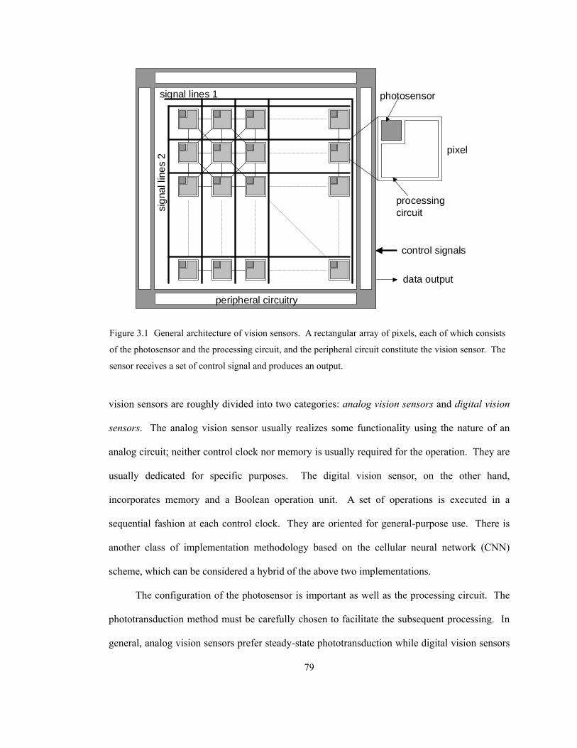
79
vision sensors are roughly divided into two categories: analog vision sensors and digital vision
sensors. The analog vision sensor usually realizes some functionality using the nature of an
analog circuit; neither control clock nor memory is usually required for the operation. They are
usually dedicated for specific purposes. The digital vision sensor, on the other hand,
incorporates memory and a Boolean operation unit. A set of operations is executed in a
sequential fashion at each control clock. They are oriented for general-purpose use. There is
another class of implementation methodology based on the cellular neural network (CNN)
scheme, which can be considered a hybrid of the above two implementations.
The configuration of the photosensor is important as well as the processing circuit. The
phototransduction method must be carefully chosen to facilitate the subsequent processing. In
general, analog vision sensors prefer steady-state phototransduction while digital vision sensors
signal lines 1
sig
nal l
ine
s 2
photosensor
processingcircuit
control signals
data output
peripheral circuitry
pixel
Figure 3.1 General architecture of vision sensors. A rectangular array of pixels, each of which consists
of the photosensor and the processing circuit, and the peripheral circuit constitute the vision sensor. The
sensor receives a set of control signal and produces an output.
80
prefer phototransduction based on charge integration.
In the following section, various types of phototransduction methods are reviewed first.
Then the type of processing circuitry, including analog, digital, or CNN schemes, is explained.
Based on these observations, a new mixed-mode processing scheme will be proposed.
3.1.1 Phototransduction
The first task of vision sensors is phototransduction, which converts the intensity of the
incoming light into an electrical signal. The most popular device for phototransduction is the
CCD (Charge Coupled Device), which is basically an analog shift register. The advantages of a
CCD are its high sensitivity, low noise, high fill-factor, and good matching [1][2]. However,
there are several disadvantages as well. First, CCD consumes a considerable amount of power:
it has to drive a large capacitance; it is inherently difficult to lower the voltage due to the need
of creating a deep depletion region under the gate. Second, a clocking scheme is complicated:
multiple voltages have to be applied with high speed to enable nearly perfect charge transfer.
Third, CCD process is not compatible with CMOS process, which is widely accessible and
well-understood technology suitable for the implementation of on-chip functions.
Although phototransduction can be carried out in several ways even with CMOS
processes, a higher noise level than that of CCD has limited its use in imager applications
despite several advantages such as random access capability, simple clocking scheme,
integration with on-chip processing functions. The most dominant noise source is a fixed
pattern noise, which is generated due to mismatch in transistors used at each pixel. However,
ever increasing demands for low power consumption, together with new technological
improvements such as correlated double sampling [3][4] to decrease the noise level, have
attracted lots of attention toward CMOS as an alternative technology for imager applications.
Most vision sensors have been implemented using CMOS processes mainly due to its capability
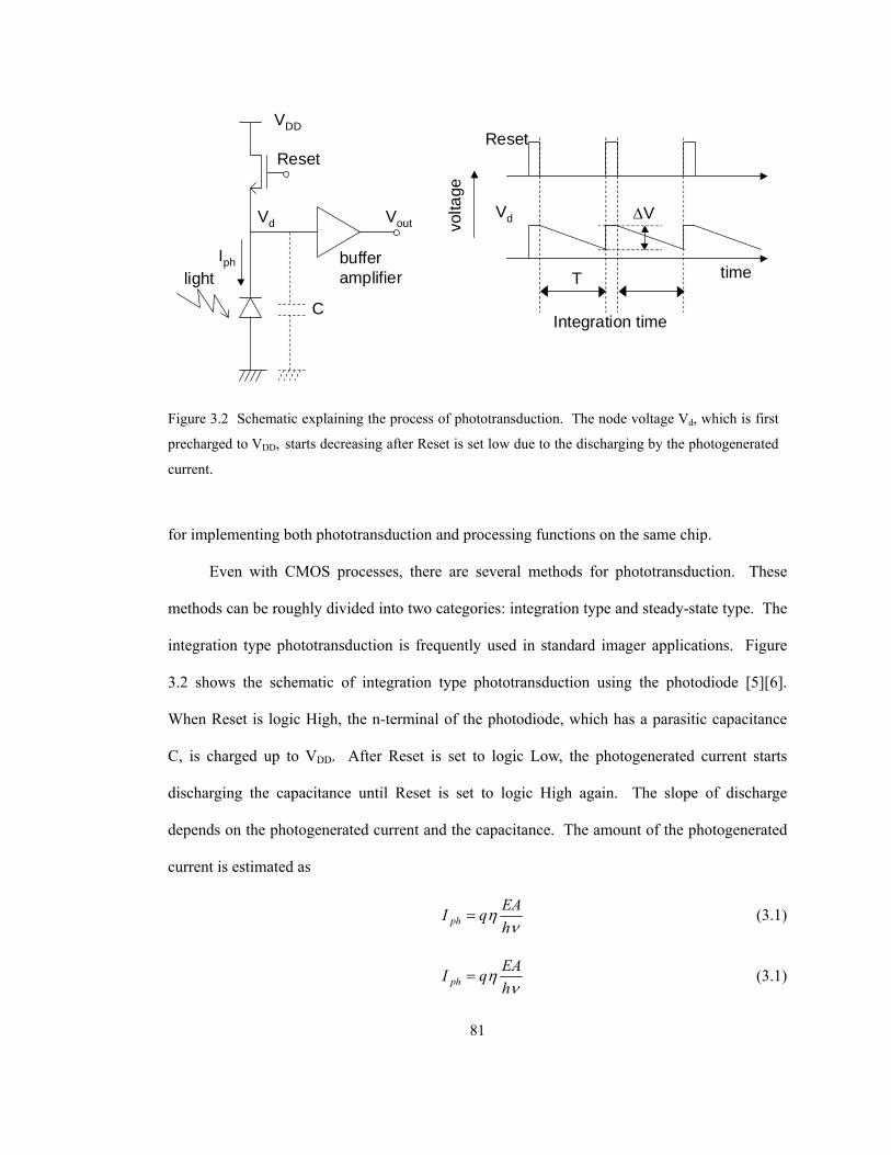
81
for implementing both phototransduction and processing functions on the same chip.
Even with CMOS processes, there are several methods for phototransduction. These
methods can be roughly divided into two categories: integration type and steady-state type. The
integration type phototransduction is frequently used in standard imager applications. Figure
3.2 shows the schematic of integration type phototransduction using the photodiode [5][6].
When Reset is logic High, the n-terminal of the photodiode, which has a parasitic capacitance
C, is charged up to VDD. After Reset is set to logic Low, the photogenerated current starts
discharging the capacitance until Reset is set to logic High again. The slope of discharge
depends on the photogenerated current and the capacitance. The amount of the photogenerated
current is estimated as
ν
ηhEAqI ph = (3.1)
ν
ηhEAqI ph = (3.1)
VDD
light
ResetReset
VdVd
time
Integration time
volta
ge
Vout
TIph
C
buffer amplifier
∆V
Figure 3.2 Schematic explaining the process of phototransduction. The node voltage Vd, which is first
precharged to VDD, starts decreasing after Reset is set low due to the discharging by the photogenerated
current.
82
where q is the charge per electron ( 19106.1 −× [C]), η is the quantum efficiency, E is the
irradiance, A is the area of the photodiode, h is the Plank constant, ν is the frequency. The
voltage drop is represented as a function of the integration time T:
ddd
phph
CET
hq
ACT
hEAq
ACTI
CTI
Vνη
νη ====∆
1 (3.2)
where C is the total parasitic capacitance, Cd is the capacitance of the depletion region per unit
area. To get a rough idea about the amount of Iph and ∆V, the following figures are substituted
for eqns. (3.1) and (3.2): A = 5 × 5 = 25 µm2; Cd = 1 [fF/µm2]; E = 0.1 [W/m2]8; η = 0.4; T = 33
[msec]. The photogenerated current and the resultant voltage are 0.48 pA and 0.63 V,
respectively. Note that the amount of photogenerated voltage is independent of the area of the
photodiode. This is desirable for further shrinking of the photosensor area to meet the demand
for higher pixel densities on chip.
Another phototransduction method belonging to the integration type is reported [3]. This
method uses photogate, which is actually made of polysilicon, and has some similarity to CCD.
Electrons generated by light illumination are accumulated under the photogate while the gate
voltage is maintained at VDD. After some integration time, the gate voltage is brought down to
GND to transfer the accumulated charge to the floating diffusion node (FD), which is initially
set to VDD. The transfer of electrons lowers the voltage of FD, which is detected by a source
follower. Correlated double sampling is possible by reading the signal twice. First reading is
carried out when the floating node is connected to VDD, and the second reading is carried out
after the accumulated electrons are transferred. The result of each reading is stored on two
capacitors to produce a differential output, which is free from noise.
The second category of phototransduction method, which is steady-state type, simply
8 The irradiance of typical office lighting is 1 W/m2. The value of 0.1 W/m2 is used as an estimate of the
intensity of the light reflected from an object.

83
uses a current output of a photodiode or a phototransistor. This type of phototransduction
scheme is mainly used in analog vision sensors for the following reasons. First, no external
clocking is necessary to obtain the signal: the output becomes available immediately after light
falls on the photodiode. This is suitable for analog implementation, which usually operates in a
continuous mode without any control clocks.
The phototransistor has been more preferably used than the photodiode simply because of
its higher current sensitivity. Figure 3.3 shows the structure of the phototransistor [7]. Note
that the base is left floating. It has been implemented using the parasitic aspects of CMOS
processes. When the light falls on the phototransistor region, electron-holes pairs are created
underneath. Electrons generated in the base region are swept to the emitter region while holes
generated in the emitter region are swept into the base region due to the built-in potential.
Carriers within a diffusion length contribute to this action. The same kind of action takes place
at the base-collector boundary. As a result of this distribution process of carriers, the base
region becomes more negatively charged, lowering the emitter-base potential barrier. This
further increases the flow of holes from the emitter to the base. The gain of this process, current
p+
n-well
p-substrate
light
p+ p+ p+p+
light IphIph
Figure 3.3 Structure of the phototransistor. The phototransistor is formed vertically by defining p+
emitter region in the n-well. The n-well serves as the base while the p-substrate works as the collector.
The emitter region is defined in a stripe manner for allowing the light to easily reach the base region.
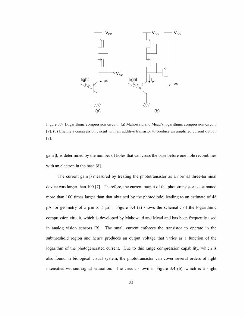
84
gain β, is determined by the number of holes that can cross the base before one hole recombines
with an electron in the base [8].
The current gain β measured by treating the phototransistor as a normal three-terminal
device was larger than 100 [7]. Therefore, the current output of the phototransistor is estimated
more than 100 times larger than that obtained by the photodiode, leading to an estimate of 48
pA for geometry of 5 µm × 5 µm. Figure 3.4 (a) shows the schematic of the logarithmic
compression circuit, which is developed by Mahowald and Mead and has been frequently used
in analog vision sensors [9]. The small current enforces the transistor to operate in the
subthreshold region and hence produces an output voltage that varies as a function of the
logarithm of the photogenerated current. Due to this range compression capability, which is
also found in biological visual system, the phototransistor can cover several orders of light
intensities without signal saturation. The circuit shown in Figure 3.4 (b), which is a slight
light Iph light Iph Iout
Vout
VDD VDD VDD
(a) (b)
Figure 3.4 Logarithmic compression circuit. (a) Mahowald and Mead’s logarithmic compression circuit
[9]. (b) Etienne’s compression circuit with an additive transistor to produce an amplified current output
[7].

85
modification of the circuit in (a) [7], is able to produce an amplified current output in the µA
order, while still maintaining the capability of covering a broad range of light intensities.
To conclude this subsection, there are mainly two types of phototransduction methods.
The photosensor in the first category performs phototransduction by charge integration and has
the following characteristics: (1) the sensitivity can be controlled by the integration time;. (2)
the shrinking of the pixel size does not decrease the output voltage; (3) clocks are necessary for
the operation. The photosensor in the second category produces a steady-state output current or
voltage, which can be just a current output of a photodiode/phototransistor or its converted form
by some processing. This type of sensor has the following characteristics: (1) the output is
immediately available after the light falls on the sensor; (2) logarithmic range compression is
possible by operating the transistor in the subthreshold region; (3) no external clock is required.
Starting from the next subsection, various types of implementation method for the
processing circuit is discussed with some reference to the phototransduction method.
3.1.2 Processing circuit – analog implementation
The first analog vision sensor was developed by a group led by Carver Mead at Caltech
[8]. The fabricated sensor is called silicon retina, which has been cited frequently by
researchers involved in this field. Their motivation was to model and implement the first stage
of retinal processing onto a silicon chip. The processing that takes place in the outer plexiform
layer of the retina is explained in the previous chapter. Briefly, the photoreceptor output, which
is proportional to the logarithm of the light intensity, is spatially and temporally averaged by the
horizontal cells. The output of the bipolar cells is proportional to the difference between the
photoreceptor signal and the horizontal cell signal. This results in the concentric ON-center
type receptive field: the light which falls onto the center area excites the bipolar cell while the
light which falls onto the periphery inhibits the bipolar cell. This receptive field responds well
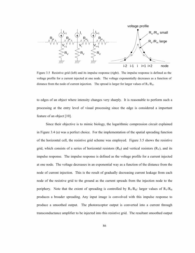
86
to edges of an object where intensity changes very sharply. It is reasonable to perform such a
processing at the entry level of visual processing since the edge is considered a important
feature of an object [10].
Since their objective is to mimic biology, the logarithmic compression circuit explained
in Figure 3.4 (a) was a perfect choice. For the implementation of the spatial spreading function
of the horizontal cell, the resistive grid scheme was employed. Figure 3.5 shows the resistive
grid, which consists of a series of horizontal resistors (RH) and vertical resistors (RV), and its
impulse response. The impulse response is defined as the voltage profile for a current injected
at one node. The voltage decreases in an exponential way as a function of the distance from the
node of current injection. This is the result of gradually decreasing current leakage from each
node of the resistive grid to the ground as the current spreads from the injection node to the
periphery. Note that the extent of spreading is controlled by RV/RH: larger values of RV/RH
produces a broader spreading. Any input image is convolved with this impulse response to
produce a smoothed output. The photoreceptor output is converted into a current through
transconductance amplifier to be injected into this resistive grid. The resultant smoothed output
RH RH RHRH
RV RV RV
Ii Ii+1Ii-1
Vi-1 Vi Vi+1
i i+1 i+2i-1i-2
voltage profile
RV /RH small
RV /RH large
node Figure 3.5 Resistive grid (left) and its impulse response (right). The impulse response is defined as the
voltage profile for a current injected at one node. The voltage exponentially decreases as a function of
distance from the node of current injection. The spread is larger for larger values of RV/RH.
87
is then subtracted from the photoreceptor output to produce the difference signal, which
corresponds to the bipolar cell output in biology. The fabricated sensor showed a good
resemblance to the biological retina in terms of spatial and time response.
Several researchers have tried to enhance the quality of smoothing by the resistive grid.
The first attempt is characterized by the use of the so-called resistive fuse [11][12]. The
resistive fuse acts as a normal resistor to produce a smoothed image when the voltage difference
between neighboring pixels is not very large. When the voltage difference becomes larger than
a specified threshold, indicating that this point is likely to correspond to the boundary of an
object, the resistive fuse shuts off the connection to separate these two regions. As a result of
the above action, the smoothing takes place in each segmented region while the edge is kept
sharp since blurring does not take place. The second attempt was to use the Gaussian function
instead of a conventional exponentially decaying function as a convolution kernel [13]. The
cusp shape of the exponentially decaying function, which has a discontinuity in derivative at the
center, would produce undesirable results when this function is applied to a noisy image and
then followed by edge detection. The Gaussian kernel was realized by connecting a pixel to the
next-nearest pixels by the negative resistance in addition to the commonly used connection
between nearest neighbors.
Boahen and Andreou reported another type of implementation of the smoothing and
subsequent edge detection function [14]. They developed a silicon retina, which is even simpler
than Mead’s retina but more closely parallels biological counterpart. In addition to the resistive
grid that mimics signal spreading due to the bipolar cell, they also implemented the signal
spreading through a photoreceptor layer, which takes an input current directly from the
phototransistor. They also realized mutual interaction between these two resistive grids,
excitatory action from the photoreceptor layer to the horizontal cell layer, and the inhibitory
action from the horizontal cell layer to the photoreceptor layer. These bilateral interactions are
88
implemented in a smart way using two transistors facing each other. This circuit is considered
the special case of the winner-take-all circuit proposed by Lazzaro [15] where strength of the
horizontal interaction is weakened due to the resistance which lies between pixels.
It should be mentioned that one of the reasons why research activity on vision sensors
based on the resistive grid scheme was so high is the close relationship between the resistive
grid and the regularization theory [16]. Several problems in early vision can be mapped into the
resistive grid scheme. The solution is obtained by simply getting the network to reach the
steady state, which corresponds to the state of the minimum energy dissipation.
Most of the above mentioned studies employ transistors operating in the subthreshold
region. The main advantage of using the subthreshold region is its low power consumption. In
addition, the exponential relationship between the gate voltage and the drain current can be
useful for compact implementation for complex computations [8][17]. However, those devices
suffer from severe transistor mismatch effect and the operational speed is slow due to the small
current. Based on these observations, Etienne-Cummings has designed an edge detection
circuit, which serves as a front-end for his motion detection sensor, in the strong inversion
region [7]. Edge detection function is realized by a resistive grid and an Opamp, which is used
to compute the difference between the input image and the smoothed image.
Another important image feature that has been detected by analog vision sensors is
orientation of lines and edges. The importance of orientation detection can be found in biology
as described in the previous chapter. An array of orientation sensors has been reported by
several researchers. Camp has fabricated an orientation sensor which consists of 8 × 8 pixels
[18]. Each orientation sensor has six outputs, corresponding to six orientations (0 to o150 by
o30 interval). The largest output indicates the orientation of the image that falls onto the
orientation sensor. Each of these six outputs is produced by summation of currents from each
89
pixel with appropriate weights. These weights are chosen so that the resultant receptive field
forms a first-order Gabor function. The Gabor function has some directionality and hence
responds most to an image aligned along the preferential direction. This is in contrast to the
concentric receptive field realized for smoothing purposes. These orientation sensors are
combined in the second layer to detect a specific curvature. Although this study showed a good
example of feature detection based on decomposed oriented segments, each orientation sensor is
still too large and complicated to enable larger array configuration.
A simplified orientation sensor with lower orientation resolution was reported by
Nishimura [19]. Instead of using a sophisticated receptive field, the illumination pattern defined
by which photosensor located at the four corners of a pixel is under illumination, was used to
encode orientation. A sensor chip which consists of a 6 × 6 array of these orientation sensors
was fabricated. The fabricated sensor was able to successfully decompose several images
projected on the sensor into four orientation planes. Almost the similar concept, but slightly
different approach, was demonstrated by Lin [20]. They have used hydrogenated amorphous
silicon technology to implement four pin diodes of trapezoidal shape placed at the edge of the
pixel. The orientation was calculated by using the current output from these photodiodes. At
each sensor, which is part of the fabricated 8 × 8 array, the orientation was locally calculated
for the image projected on the sensor. In contrast to refs. [18][19], the sensor output is
represented as an analog continuous value, which may be difficult to process at later stages for
the detection of higher features. The similar idea of calculating the orientation from the four
position sensitive devices is found in ref. [21].
The directional receptive field can be realized by giving different voltages to the gate of
the transistors for horizontal connection in different orientations. However, the rapidly
decreasing nature of the exponential function does not produce a large receptive field. Venier et
al. have replaced vertical resistors forming a resistive grid with current sources so that the

90
voltage decaying profile becomes linear instead of an exponential profile [22]. The voltage is
compared to a given threshold to produce a binary-valued receptive field. The experimental
result showed that by properly controlling the gate voltages of horizontal resistors in three
directions and choosing the proper injection current level, the orientation and the size of the
receptive field could be well controlled.
Instead of preparing a set of receptive fields for different orientations, it is possible to
estimate the orientation based on the two responses, one obtained from the receptive field for
o0 and the other for o90 . Etienne-Cummings et al. have demonstrated this idea in ref. [23].
The receptive field for o0 is represented as a 33× template matrix, i.e., a set of weights
multiplied for 33× neighbors for current summation. The template consists of three horizontal
2's in the center row and three –1's both in the top row and in the bottom row. The receptive
field for o90 is obtained by rotating the o0 receptive field by o90 . It was shown that the
response from the o0 receptive field is largest for o0 line and linearly decreases as the
orientation increase up to o45 . Above o45 , the response levels off at almost zero. On the
other hand, the response of the o90 receptive field is almost zero up to o45 but starts linearly
increasing to reach the maximum at o90 stimulus. At each pixel, the local orientation was
reconstructed from these two outputs. The size and the configuration of the receptive field are
programmable by a smart circuit configuration. The circuit for generating the receptive field is
placed outside the pixel array and the computation is performed at the time of read-out. The
proposed scheme thus converts the computation performed in the space domain in most vision
sensors to the time-domain, enabling the increase of the pixel density and providing exactly the
same kernel for every pixel without suffering from transistor mismatch. The idea of
programmable kernel was also demonstrated in a different fashion by Kyuma et al. [24]. Their

91
sensor consists of a two-dimensional variable sensitivity photosensors. The convolution kernel
is limited to one-dimension and is given as the voltage pattern along the column, which controls
the sensitivity of the photosensor. The convolution is computed by the current summation; the
computation result is scanned along all column lines simultaneously.
The orientation detection explained so far is a local computation: each pixel detects the
orientation using the information projected on itself and neighbors. The extent of neighbors
being used for calculation determines the size of the receptive field. In other words, this type of
processing is pixel-based. In contrast to these local computations, a principal orientation of an
object projected on the entire chip is sometimes useful. Standley et al. have fabricated a sensor
that detects the centroid and orientation of an object [25]. The centroid and the orientation can
be defined using the first order and the second order moment. The fabricated sensor produces a
set of current, which is the result of some computation using the two-dimensional resistive grid
for the given intensity distribution. The centroid and the orientation can be reconstructed from
these outputs. This type of processing can be referred to as object-based, since the detected
quantities, centroid and orientation, are the attributes of each object.
Several papers have been reported on these types of object-based processing. Liu and
Harris reported the concept of the dynamic wire which can be used for different calculations
[26]. The concept of dynamic wire is: configuring the switches in a two-dimensional network
to connect a group of pixels that share a common property, and then utilizing the resultant
dynamic connections for computation. By closing the switches that correspond to the edge of
an object, pixels on the contour are connected with each other. From a set of these mutually
connected pixels, each having a current source, a leader pixel is arbitrary chosen to establish a
current path to the ground. The total current, which flows into the ground, is proportional to the
number of pixels belonging to the contour.
Luo et al. have presented an interesting sensor which performs figure-ground segregation
92
by labeling all points inside a given contour with one voltage and all remaining points outside
this contour with another voltage [27]. The resistive network is configured with communication
switches. The input of the sensor is again the contour, or the binary edge map. A pixel
corresponding to the contour is isolated from the surrounding pixels. This is the opposite action
that takes place on the above-mentioned sensor for contour length computation. The pixels
inside an object are connected with each other and isolated from the surrounding region. The
current injected at the center, which is based on the assumption that the object is always
centered, spreads through a resistor path until it hits the contour where the switch is shut off. If
the contour is broken at some points, the current spreads outside to seal off the incomplete
contour, isolating the object from the background.
Nishimura et al. have presented a sensor that counts the number of objects [28]. The
sensor produces a current that is proportional to the number of objects. The object is defined as
a set of mutually connected pixels in either horizontal or vertical direction. Two adjacent pixels
in either horizontal or vertical direction are connected with each other when both of these two
pixels are under illumination. Thus the region under illumination is defined as one object and
isolated from the surroundings. The winner-take-operation is performed within each object to
select one winner. A current that is proportional to the number of winners and hence
proportional to the number of objects is produced. The sensor not only counts the number of
objects but also measures the size of each object. This is possible because the current at the
winning pixel collects all the current from other pixels inside the object and thus represents the
object size.
Several types of analog vision sensors have been reviewed above. It was observed that
most of these vision sensors favor phototransistors as a photosensor due to its operation in the
subthreshold region and the steady-state output. In terms of functionality, several functions
such as smoothing, edge detection, orientation detection, and detection of object-based features

93
have been implemented. The beauty of analog processing lies in its simplicity. By properly
mapping the target problem into the voltage and current domain, several functions are realized
with much smaller number of circuit elements than the digital counterpart. For example, the
resistive grid scheme allows the interaction between pixels that are several pixels apart although
the wiring is limited to nearest neighbors. This type of interaction is not easy to realize in
digital implementation, which usually necessitates the direct wiring between pixels that are
several pixels apart, thus drastically complicating the layout. Another example that shows the
advantages of analog implementation is the orientation computation performed in Standley’s
sensor [25]. This computation would be difficult to implement in digital fashion since it is a
fairly complex computation. A small number of circuit elements at each pixel naturally leads to
less area and lower power consumption. The number of control lines and clock lines is
significantly smaller than the digital implementation, which also contributes to lower power
consumption.
However, the analog vision sensors are not very suitable for performing different types of
processing in an iterative manner, which is required for the proposed feature detection
algorithm, due to lack of a memory. However, the nature of analog processing which naturally
maps the interaction between pixels into the form of the receptive field is attractive and will be
considered again later in this work.
3.1.3 Processing circuit – digital implementation
In contrast to the analog vision sensors, most of which are dedicated for specific
purposes, the digital vision sensors are intended for more general purposes. This is possible by
the use of the SIMD (Single Instruction Multiple Datastream) architecture, which assigns a
processor per each pixel. Researches on digital vision sensors have been conducted mainly by
three different groups.

94
Bernard et al. have fabricated a digital vision sensor, which is probably the simplest of
this kind in terms of hardware [29]. The binary image is obtained by thresholding the output
voltage of a p-n junction photodiode operated in the integration mode. Each pixel has only 28
transistors for processing purposes. A set of basic Boolean operations is defined for three
memories. Despite the use of a slightly outdated 2 µm CMOS technology, the fabricated sensor
contains a relatively large number of pixels, 65 × 76 pixels, each measuring 100 µm × 80 µm.
The maximum operational clock frequency was 20 MHz. Several operations such as erosion,
edge detection were implemented as a sequence of basic Boolean operations. The execution
time was in the order of µsec. More complex operations such as thinning resulted in the
execution time in the order of msec. The relatively large execution time is required because a
large number of operations, each of which is very simple but functionally limited, has to be
performed. This example clearly shows the trade-off between the simplicity of the operation at
each pixel and the execution time. Simplicity leads to increased pixel density and higher speed
per operation but needs a lot of operations to perform a specific task. On the other hand,
generality leads to reduced number of operation cycles but requires more pixel area, resulting in
lower density.
Another type of digital vision sensors, which is based on the NSIP (Near Sensor Image
Processing) concept, has been designed by Eklund et al. [30]. The sensor contains 32 × 32
pixels in an area of 25 mm2, each pixel measuring 118 µm × 118 µm and containing 97
transistors. No explicit ALU (Arithmetical and Logical Unit) is implemented at each pixel.
Instead, Boolean operations can be performed by properly combining NAND operation, which
is implemented as a precharged logic. For phototransduction, the integration type photosensor
was employed again but in a slightly different manner. Gray level information is obtained by
counting the number of readout until the output voltage of the photosensor, which keeps
95
decreasing, reaches a certain threshold value, instead of measuring the voltage after a certain
integration time. Six memories are used as a counter to store this gray level information.
Furthermore, the global operation, such as counting the number of pixels meeting a specific
requirement, can be executed. The sensor realizes a high spatial density while achieving basic
neighborhood processing as well as global processing.
The third type of digital vision sensors was reported by Ishikawa's group at the University
of Tokyo [31]-[33]. The latest version of the vision sensor was realized in an array of 16 × 16
pixels in a 2.4 mm × 2.4 mm chip area using CMOS 0.35 µm technology. Each pixel contains
510 transistors, which is significantly larger than that implemented in the sensors mentioned
above. As this number suggests, this sensor has the most general processing capability. There
are 24 memories included in each pixel. The sensor performs A/D conversion by using the
same procedure as is employed in the NSIP chip. An 8 bit arithmetic operation is possible by
bit serial processing. The communication between 4-neighbors is realized by memory mapped
I/O. One operation cycle is divided into four subcycles to save the number of control lines,
although this time-division quadruples the processing time for one instruction. The fabricated
sensor was able to perform fairly complex operations such as line thinning in the order of
microseconds. It was also used for the purpose of high speed target tracking.
As the above three examples indicate, digital implementation favors phototransduction in
the integration mode. It is partly because there have not been so much motivation to mimic
biological range compression which is obtained by operating transistors in the subthreshold
region, and partly because that inherent necessity of clocking in the digital implementation
facilitates the phototransduction by integration. The only problem is that phototransduction
takes time, in the order of msec in the normal lighting conditions. This seems to contradict with
the demand for high-speed operation. The digital processing time turns out to be a mere
fraction of the entire processing time that includes phototransduction in addition to the
96
processing time.
The other key point of the digital vision sensors is how to find the optimal balance
between processing generality and high spatial density. Although it depends on the target
application, the trend seems to support having more generality at each pixel without too much
degrading the spatial resolution, which is boosted by the continuing drive for smaller feature
size. For examples, a sensor which has practically useful number of pixels, say, 64 × 64, would
be possible to implement on chip based on Ishikawa’s architecture.
However, the present configuration of the vision sensors is not very suitable for the
implementation of the feature detection algorithm for the following reasons. First, the
interaction between pixels is limited to 4-neighbors, meaning that the information on diagonal
pixels has to be retrieved in two steps. For the purpose of feature detection, which needs
diagonal information as well as horizontal and vertical information, communication between
diagonal pixels is crucial. Second, even within the interaction between 4-neighbors, the vision
sensors cannot perform the logical operation using all these values at once. For example,
Ishikawa’s vision sensor can take only two inputs for one Boolean operation, meaning that at
least four operations are required for the operation based on its 4-neighbors. This is because the
digital vision sensors are built on the framework of standard Boolean operations, which is
purely arithmetic and does not have any concept of describing the interaction between pixels.
3.1.4 Processing circuit – CNN implementation
The cellular neural network (CNN) is a powerful framework for systematic formulation
of low-level image processing functions [34] as explained in the previous chapter. Several
sensors have been fabricated based on this paradigm [35]-[37]. The CNN sensor designed by
Domínguez-Castro [37] seems to be the most sophisticated one and hence explained below as a
representative example of this type of implementation. The CNN computation is realized in an
97
array form of nonlinear dynamic analog processing units, arranged on regular grids where direct
interactions among cells are usually limited to 3 × 3 neighbors. In addition to the internal
analog operations in continuous time, an iterative operation based on the external clock is
possible. This implementation is based on the CNN universal machine (CNN-UM) [38], which
is an extended concept of the standard CNN [34], and can be considered a hybrid of the analog
vision sensor and the digital vision sensor.
The sensor is intended for processing a binary image. Phototransduction was carried out
using a phototransistor arranged in Darlington configuration: the output of the phototransistor is
connected to the base of the vertical pnp transistor for further amplification. The output current
was thresholded to produce a binary image. The threshold was automatically adjusted to the
average of the photocurrent on the entire array of pixels to avoid an image of completely black
or completely white pixels.
The processing function is determined by 19 analog coefficients whose values are
programmable with 7-bit accuracy. These 19 analog coefficients completely determine the
evolution pattern of the pixel: nine coefficients are necessary for the feedback template; the
other nine for the control template; and the remaining one for the offset term (see eqn. (2.24)).
The sensor can store a sequence of operations in the memory. The sensor also has some digital
flavor by incorporating four memories per pixel and allowing Boolean operations between these
memories. This sensor is very powerful since operations based on templates known for
different image processing applications can be executed on-chip. However, the processing
speed is not very fast: each operation takes about 2 µs. This amount of time is necessary for the
network to settle into the steady state.
3.1.5 The selected architecture
The three types of implementation schemes for on-chip processing, which are closely
98
related to the method of phototransduction, have been reviewed. The analog vision sensor is
able to define cell interaction by either resistive grid or programmable kernels, but is not very
suitable for iterative processing. The digital vision sensor, on the other hand, is suitable for
iterative processing. However, the computation using 4-neighbors or 8-neighbors in one step is
not easy to implement due to its gate-level based Boolean logic. Compared to these two
schemes, the sensor based on the CNN-UM framework works in a hybrid way: it specifies the
pixel interaction by the programmable kernel; the operation can be executed in an iterative
fashion for multiple memories. Therefore, it is an appropriate architecture for the
implementation of the feature detection algorithm. It is a natural consequence since the
proposed feature detection algorithm, which is based on the template matching scheme, is
considered the special case of the cellular neural network.
The implementation, however, can be drastically simplified by getting rid of unnecessary
elements, which includes analog multipliers (synapse), circuit element associated with control
templates, and capacitors. The resultant processing circuit turns out to be a programmable
current distribution circuit and thresholding circuit with some memories for storing images.
Due to this simplification, the circuit dynamics is completely changed from the operation
governed by RC time constants to the operation governed by constant current sources.
Therefore, much faster operation is expected.
As for the selection of the phototransduction method, the phototransistor operated in the
steady-state mode (without integration) seems to be the best choice. For the present objective of
capturing an image in a binary level, the simple thresholding scheme is just enough. Range
compression capability found in most analog vision sensors is not necessary. The choice of
phototransistor over photodiode is due to its larger current. The increased current level should
work for faster charging and discharging of the thresholding node.
In summary, the considerations based on the related work on vision sensors led us to the
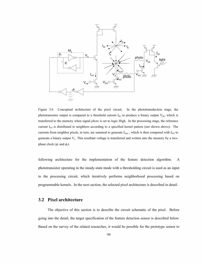
99
following architecture for the implementation of the feature detection algorithm. A
phototransistor operating in the steady-state mode with a thresholding circuit is used as an input
to the processing circuit, which iteratively performs neighborhood processing based on
programmable kernels. In the next section, the selected pixel architecture is described in detail.
3.2 Pixel architecture
The objective of this section is to describe the circuit schematic of the pixel. Before
going into the detail, the target specification of the feature detection sensor is described below.
Based on the survey of the related researches, it would be possible for the prototype sensor to
Iphφ2
φ1
Va
MaIS
IEIW
ISum
Ith2
IN
φ1
Vth2
VoIref
light
Ith1
photo
photoVph
Vth1
Vref
Figure 3.6 Conceptual architecture of the pixel circuit. In the phototransduction stage, the
phototransistor output is compared to a threshold current Ith1 to produce a binary output Vph, which is
transferred to the memory when signal photo is set to logic High. In the processing stage, the reference
current Iref is distributed to neighbors according to a specified kernel pattern (not shown above). The
currents from neighbor pixels, in turn, are summed to generate Isum , which is then compared with Ith2 to
generate a binary output Vo This resultant voltage is transferred and written into the memory by a two-
phase clock (φ1 and φ2).
100
have an array of 16 × 16 pixels, each measuring 150 µm × 150 µm, in a chip area of 3.2 mm ×
3.2 mm using CMOS 0.5 µm technology. The margin between 2.4 mm (150 µm × 16) and 3.2
mm is for peripheral circuits and for pads. If the design is successfully tested, it should be
easily scaled up to an array of 64 × 64 pixels, each measuring 100 µm × 100 µm, in a chip area
of 7.2 mm × 7.2 mm with CMOS 0.35 µm technology. This is technically feasible and the
array size of 64 × 64 would be practically useful for some applications. Therefore, the
prototype sensor is considered a small-size model for the verification of the circuit design stated
below.
3.2.1 Overall architecture
The conceptual architecture of the pixel circuit is shown in Figure 3.6. It consists of a
phototransduction circuit (shown on the right-hand side) and a processing circuit (shown on the
left-hand side). As explained before, the phototransistor is selected as a transducer element.
The output current of the phototransistor Iph is compared to a threshold current Ith1 to generate a
binary output Vph, which is always available as a steady-state output.
The processing circuit is constructed in a mixed-mode fashion in the sense that the
internal operation is performed in the analog domain while the control of the operation is
performed in the digital domain. The circuit consists of the memory and the convolution unit
with programmable kernels. The basic function is to distribute a current to neighborhood pixels
if the memory content is logic High. The distribution pattern, which corresponds to the
convolution kernel, is specified by the setting of switches along the connection path to
neighbors, which are not shown in the figure. The currents from neighboring pixels, in turn, are
summed to generate Isum and compared with Ith2 to generate a binary output Vo. This binary
voltage is then transferred through a parasitic capacitor to the memory by the use of a non-
overlapping two-phase clock (φ1 and φ2).
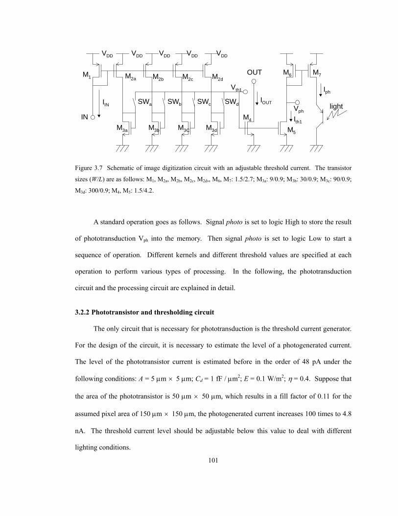
101
A standard operation goes as follows. Signal photo is set to logic High to store the result
of phototransduction Vph into the memory. Then signal photo is set to logic Low to start a
sequence of operation. Different kernels and different threshold values are specified at each
operation to perform various types of processing. In the following, the phototransduction
circuit and the processing circuit are explained in detail.
3.2.2 Phototransistor and thresholding circuit
The only circuit that is necessary for phototransduction is the threshold current generator.
For the design of the circuit, it is necessary to estimate the level of a photogenerated current.
The level of the phototransistor current is estimated before in the order of 48 pA under the
following conditions: A = 5 µm × 5 µm; Cd = 1 fF / µm2; E = 0.1 W/m2; η = 0.4. Suppose that
the area of the phototransistor is 50 µm × 50 µm, which results in a fill factor of 0.11 for the
assumed pixel area of 150 µm × 150 µm, the photogenerated current increases 100 times to 4.8
nA. The threshold current level should be adjustable below this value to deal with different
lighting conditions.
VDD
Vth1
M1 M2a M2b M2c M2d
M3a M3b M3C
M4
IIN IOUT
M3d
VDD VDD VDD VDD
SWa SWb SWc SWd
IN
OUT
Iph
light
Ith1
Vph
M5
M6 M7
Figure 3.7 Schematic of image digitization circuit with an adjustable threshold current. The transistor
sizes (W/L) are as follows: M1, M2a, M2b, M2c, M2d,, M6, M7: 1.5/2.7; M3a: 9/0.9; M3b: 30/0.9; M3c: 90/0.9;
M3d: 300/0.9; M4, M5: 1.5/4.2.
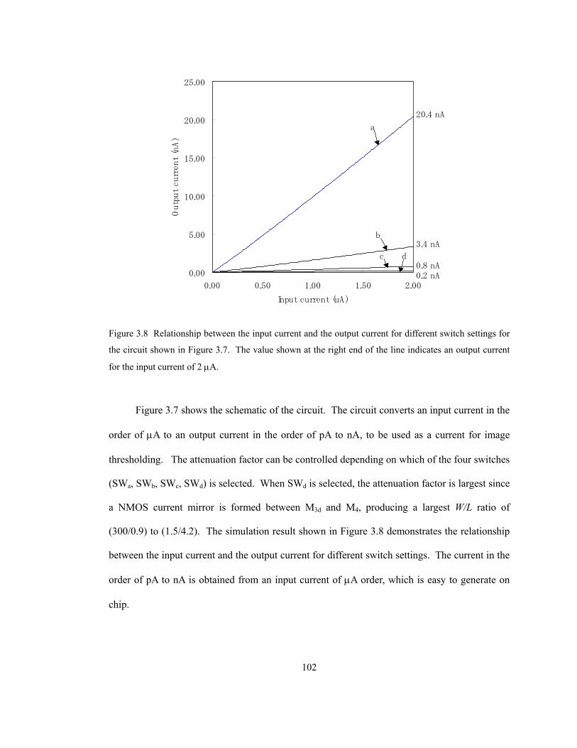
102
Figure 3.7 shows the schematic of the circuit. The circuit converts an input current in the
order of µA to an output current in the order of pA to nA, to be used as a current for image
thresholding. The attenuation factor can be controlled depending on which of the four switches
(SWa, SWb, SWc, SWd) is selected. When SWd is selected, the attenuation factor is largest since
a NMOS current mirror is formed between M3d and M4, producing a largest W/L ratio of
(300/0.9) to (1.5/4.2). The simulation result shown in Figure 3.8 demonstrates the relationship
between the input current and the output current for different switch settings. The current in the
order of pA to nA is obtained from an input current of µA order, which is easy to generate on
chip.
0.00
5.00
10.00
15.00
20.00
25.00
0.00 0.50 1.00 1.50 2.00
Input current (uA)
Output current (nA)
a
b
c d
20.4 nA
3.4 nA
0.8 nA0.2 nA
Figure 3.8 Relationship between the input current and the output current for different switch settings for
the circuit shown in Figure 3.7. The value shown at the right end of the line indicates an output current
for the input current of 2 µA.
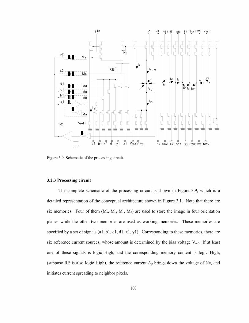
103
3.2.3 Processing circuit
The complete schematic of the processing circuit is shown in Figure 3.9, which is a
detailed representation of the conceptual architecture shown in Figure 3.1. Note that there are
six memories. Four of them (Ma, Mb, Mc, Md) are used to store the image in four orientation
planes while the other two memories are used as working memories. These memories are
specified by a set of signals (a1, b1, c1, d1, x1, y1). Corresponding to these memories, there are
six reference current sources, whose amount is determined by the bias voltage Vref. If at least
one of these signals is logic High, and the corresponding memory content is logic High,
(suppose RE is also logic High), the reference current Iref brings down the voltage of Nc, and
initiates current spreading to neighbor pixels.
Vref
Ith
IW
IS
IEIN
a1 b1 c1 d1
1
2
y2
Md
Mc
Mb
Ma
My
N1
N2
NE1 E1 SE1 S1 SW1 W 1
W 2
NW1
INE
ISE ISW
INW
NE2 SW2 NW2
x2M x
a1
b1
c1
d1
y2
C
2
2
2
1
1
1
R E
2 1
2 1
x1
1
y1
Nc
IcIsum
Vo
Vth1Vth2 E2 SE2 S2
y1n
Iref
Figure 3.9 Schematic of the processing circuit.
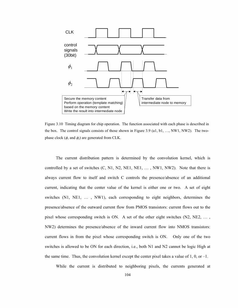
104
The current distribution pattern is determined by the convolution kernel, which is
controlled by a set of switches (C, N1, N2, NE1, NE1, … , NW1, NW2). Note that there is
always current flow to itself and switch C controls the presence/absence of an additional
current, indicating that the center value of the kernel is either one or two. A set of eight
switches (N1, NE1, … , NW1), each corresponding to eight neighbors, determines the
presence/absence of the outward current flow from PMOS transistors: current flows out to the
pixel whose corresponding switch is ON. A set of the other eight switches (N2, NE2, … ,
NW2) determines the presence/absence of the inward current flow into NMOS transistors:
current flows in from the pixel whose corresponding switch is ON. Only one of the two
switches is allowed to be ON for each direction, i.e., both N1 and N2 cannot be logic High at
the same time. Thus, the convolution kernel except the center pixel takes a value of 1, 0, or –1.
While the current is distributed to neighboring pixels, the currents generated at
φ1
φ2
CLK
controlsignals(30bit)
Secure the memory contentPerform operation (template matching)based on the memory contentWrite the result into intermediate node
Transfer data fromintermediate node to memory
Figure 3.10 Timing diagram for chip operation. The function associated with each phase is described in
the box. The control signals consists of those shown in Figure 3.9 (a1, b1, …, NW1, NW2). The two-
phase clock (φ1 and φ2) are generated from CLK.

105
neighboring pixels are accumulated on the thresholding node. The accumulated current Isum is
compared to the threshold current Ith, specified by signals Vth1 and Vth2. With these switches set
to logic Low, the threshold current is 0.5Iref. It can be increased to 1.5Iref and 2.5Iref by setting
one or two of these switches. The result of comparison is transferred to the parasitic capacitor
at the output of the inverter when clock φ1 is logic High for temporal information storage. The
stored charge is then transferred to the memory by setting φ2 to logic High. Then by bringing
down φ2 and raising φ1, the information is secured in the memory. This processing initiates a
new operation cycle since control signals are already set to logic High or Low before φ1 goes
High. Figure 3.10 shows the above-mentioned operational cycle. The operation can be
repeated as many times as specified.
There is a difference in the configuration among six memories. For memories Ma, Mb,
Mc, Md, one control signal (a1, b1, c1, d1) is used for specifying both the source (from which
memory to read) and the destination (to which memory to write), resulting in the automatic
updating of the content when some memory is selected for reading. If RE is set to logic Low,
the memory content is updated with the operation result (voltage Vo in Figure 3.9) even though
the present content is not used for computation. Memories Mx and My do not have the
restriction of automatic updating of the memory content by having separate lines for specifying
source and destination (x1, y2 for source and x2, y2 for destination). Memory My has another
useful feature. If this memory is specified as the destination of storing the operation result (y2
logic High), the automatic updating of the memory content is disabled for Ma, Mb, Mc, and Md,
making it possible to use the content of these memories for computation without affecting their
content. Another unique feature of memory My is that it can be used in an inhibitive way by
asserting signal y1n, which enables the sourcing of current flow into node Nc, resulting in the
decrease in the current that is distributed to neighboring pixels.
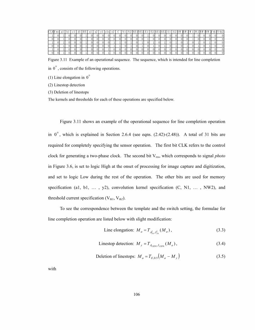
106
Figure 3.11 shows an example of the operational sequence for line completion operation
in o0 , which is explained in Section 2.6.4 (see eqns. (2.42)-(2.48)). A total of 31 bits are
required for completely specifying the sensor operation. The first bit CLK refers to the control
clock for generating a two-phase clock. The second bit Vres, which corresponds to signal photo
in Figure 3.6, is set to logic High at the onset of processing for image capture and digitization,
and set to logic Low during the rest of the operation. The other bits are used for memory
specification (a1, b1, … , y2), convolution kernel specification (C, N1, … , NW2), and
threshold current specification (Vth1, Vth2).
To see the correspondence between the template and the switch setting, the formulae for
line completion operation are listed below with slight modification:
Line elongation: )(13
13 , aIAa MTM
aa= , (3.3)
Linestop detection: )(88 , aIAy MTM
LSDLSD= , (3.4)
Deletion of linestops: ( )yaEa MMTM −= 5.0, (3.5)
with
C LKVres a1 b1 c1 d1 RE x1 x2 y1 y1n y2 C N1 N2 NE1NE2 E1 E2 SE1SE2 S1 S2 SW 1SW 2 W 1 W 2 NW 1NW 2Vth1Vth2
1 0 1 0 0 0 1 0 0 0 0 0 0 0 0 0 0 1 0 0 0 0 0 0 0 1 0 0 0 0 00 0 1 0 0 0 1 0 0 0 0 0 0 0 0 0 0 1 0 0 0 0 0 0 0 1 0 0 0 0 01 0 1 0 0 0 1 0 0 0 0 1 1 0 1 0 1 0 1 0 1 0 1 0 1 0 1 0 1 0 00 0 1 0 0 0 1 0 0 0 0 1 1 0 1 0 1 0 1 0 1 0 1 0 1 0 1 0 1 0 01 0 1 0 0 0 1 0 0 0 1 0 0 0 0 0 0 0 0 0 0 0 0 0 0 0 0 0 0 0 00 0 1 0 0 0 1 0 0 0 1 0 0 0 0 0 0 0 0 0 0 0 0 0 0 0 0 0 0 0 0
Figure 3.11 Example of an operational sequence. The sequence, which is intended for line completion
in o0 , consists of the following operations.
(1) Line elongation in o0
(2) Linestop detection
(3) Deletion of linestops
The kernels and thresholds for each of these operations are specified below.
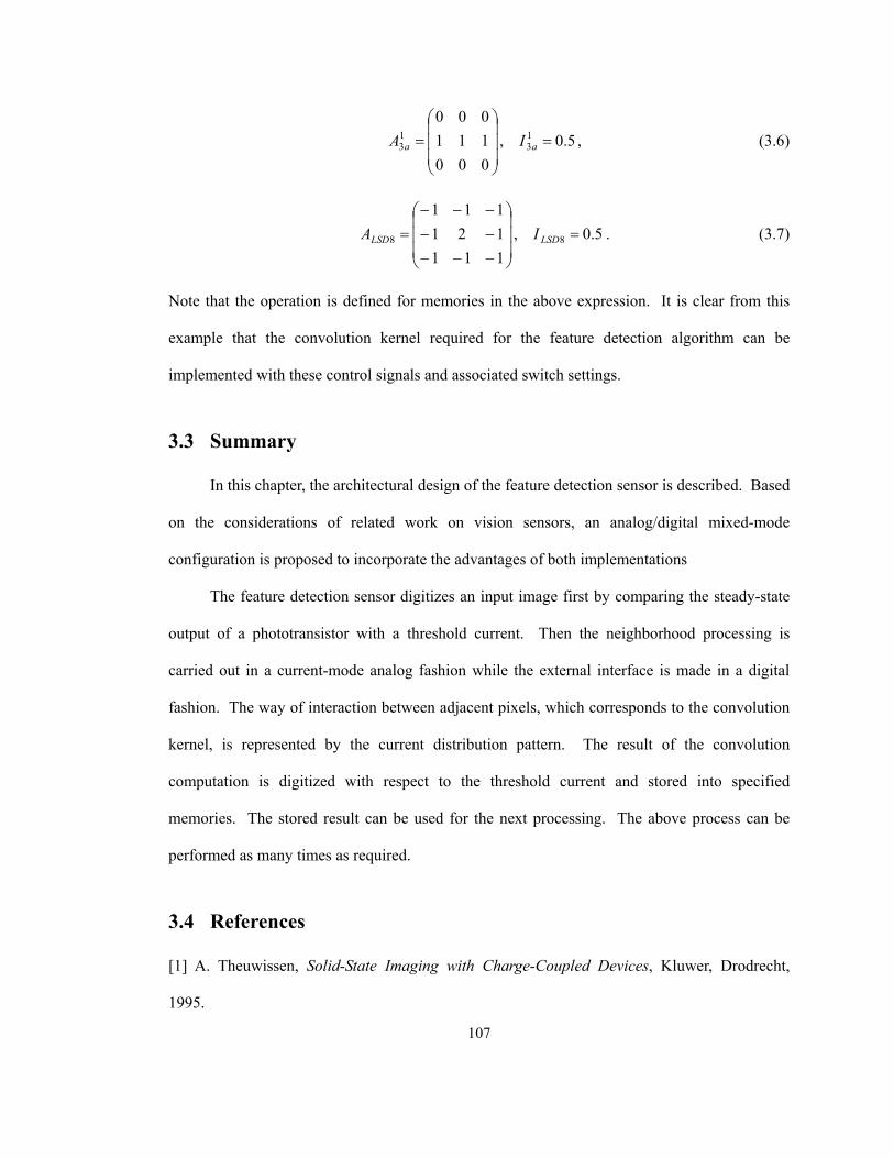
107
5.0,000111000
13
13 =
= aa IA , (3.6)
5.0,111121111
88 =
−−−−−−−−
= LSDLSD IA . (3.7)
Note that the operation is defined for memories in the above expression. It is clear from this
example that the convolution kernel required for the feature detection algorithm can be
implemented with these control signals and associated switch settings.
3.3 Summary
In this chapter, the architectural design of the feature detection sensor is described. Based
on the considerations of related work on vision sensors, an analog/digital mixed-mode
configuration is proposed to incorporate the advantages of both implementations
The feature detection sensor digitizes an input image first by comparing the steady-state
output of a phototransistor with a threshold current. Then the neighborhood processing is
carried out in a current-mode analog fashion while the external interface is made in a digital
fashion. The way of interaction between adjacent pixels, which corresponds to the convolution
kernel, is represented by the current distribution pattern. The result of the convolution
computation is digitized with respect to the threshold current and stored into specified
memories. The stored result can be used for the next processing. The above process can be
performed as many times as required.
3.4 References
[1] A. Theuwissen, Solid-State Imaging with Charge-Coupled Devices, Kluwer, Drodrecht,
1995.
108
[2] E. Fossum, “Active pixel sensors: Are CCD’s dinosaurs?,” SPIE Proc. Charge-Coupled
Devices and Solid State Optical Sensors III, (San Jose, California), vol. 1900, pp. 2-14,
February 1993.
[3] S. Mendis, S. Kemeny, R. Gee, B. Pain, C. Staller, Q. Kim, and E. Fossum, “CMOS active
pixel image sensors for highly integrated imaging systems,” IEEE J. Solid-State Circuits, vol.
32, no. 2, pp. 187-197, 1997.
[4] R. Nixon, S. Kemeny, B. Pain, C. Staller, and E. Fossum, “256× 256 CMOS active pixel
sensor camera-on-a-chip,” IEEE J. Solid-State Circuits, vol. 31, no. 12, pp. 2046-2050, 1996.
[5] C. Aw and B. Wooley, “128× 128-pixel standard-CMOS image sensor with electronic
shutter,” IEEE J. Solid-State Circuits, vol. 31, no. 12, pp. 1922-1930, 1996.
[6] O. Yadid-Pecht, R. Ginosar, Y. Diamand, “A random access photodiode array for intelligent
image capture,” IEEE Trans. Electron Devices, vol. 38, no. 8, pp. 1772-1782, 1991.
[7] R. Etienne-Cummings, “Biologically motivated analog VLSI systems for optomotor tasks”,
Ph. D. dissertation, University of Pennsylvania, Philadelphia, PA, 1994.
[8] C. Mead, Analog VLSI and Neural Systems. Addison Wesley, Reading, MA, 1989.
[9] C. Mead and M. Mahowald, "A silicon model of early visual processing," Neural Networks,
vol. 1, pp. 91-97, 1988.
[10] D. Marr, Vision, W. H. Freeman and Company, New York, 1982.
[11] J. Harris, C. Koch, J. Luo, and J. Wyatt, “Resistive fuses: analog hardware for detecting
discontinuities in early vision,” Analog VLSI Implementation of Neural Systems, (C. Mead and
M. Ismail, eds.), Kluwer, Norwell, MA, pp. 27-55, 1989.
[12] P. Yu, S. J. Decker, H. Lee, C. Sodini, and J. Wyatt, “CMOS resistive fuses for image
smoothing and segmentation,” IEEE J. Solid-State Circuits, vol. 27, no. 4, pp. 545-553, 1992.
[13] H. Kobayashi, J. White, “An active resistor network for Gaussian filtering of images,”
IEEE J. Solid-State Circuits, vol. 26, no. 5, pp. 738-748, 1991.

109
[14] K. Boahen and A. Andreou, “A contrast sensitive silicon retina with reciprocal synapses,”
Advances in Neural Information Processing Systems, (J. Moody, J. Hanson, R. Lippmann, eds.),
vol. 4, Morgan Kaufmann, San Mateo, CA, pp. 764-772, 1992.
[15] J. Lazzaro, S. Ryckebusch, M. Mahowald, and C. Mead, "Winner-take-all networks of
O(N) complexity,” Advances in Neural Information Processing Systems vol. 1, (David S.
Touretzky, ed.), Morgan Kaufmann Publishers, 1989.
[16] T. Poggio, V. Torre, and C. Koch, “Computational vision and regularization theory,”
Nature, vol. 317, pp. 314-319, 1985.
[17] A. Andreou, K. Boahen, P. Pouliquen, A. Pavasovic, R. Jenkins, and K. Strohbehn,
“Current-mode subthreshold MOS circuits for analog neural systems,” IEEE Trans. Neural
Networks, vol. 2, no. 2, pp. 205-213, 1991.
[18] W. Camp and J. Van der Spiegel, "A silicon VLSI optical sensor for pattern recognition,"
Sensors and Actuators A, vol. 43, pp. 188-195, 1994.
[19] M. Nishimura, K. Sunamura, and J. Van der Spiegel, “A silicon VLSI optical sensor for
image decomposition,” Sensors and Actuators A, vol. 69, pp. 53-61, 1998.
[20] K. Lin and S. Lee, "Active hollow four quadrant orientation detector array for application
to pattern recognition," IEEE Trans. Electron Devices, vol. 42, no. 7, 1995.
[21] M. Nishimura and J. Van der Spiegel, “A compact line and edge orientation detection
sensor,” Sensors and Actuators A, vol. 40, pp. 217-225, 1994.
[22] P. Venier, A. Mortara, X. Arreguit, E. Vittoz, "An integrated cortical layer for orientation
enhancement," IEEE J. Solid-State Circuits, vol. 32, no. 2, pp. 177-186, 1997.
[23] R. Etienne-Cummings, D. Cai, "A general purpose image processing chip: orientation
detection," Advances in Neural Information Processing Systems, (M. Jordan, M. Kearns, S.
Solla eds.), vol. 10, MIT Press, pp. 865-871, 1998.
[24] K. Kyuma, E. Lange, J. Ohta, A. Hermanns, B. Banish, and M. Oita, “Artificial retina –
110
fast, versatile image processors,” Nature, vol. 372, pp. 197-198, 1994.
[25] D. Standley, “An object position and orientation IC with embedded imager,” IEEE J. Solid-
State Circuits, vol. 26, no. 12, pp. 1853-1859, 1991.
[26] S. Liu and J. Harris, “Dynamic wires: An analog VLSI model for object-based processing,”
International Journal of Computer Vision, vol. 8, no. 3, pp. 231-239, 1992.
[27] J. Luo, C. Koch, and B. Mathur, “Figure-ground segregation using an analog VLSI chip,”
IEEE Micro, vol. 12, pp. 45-57, December 1992.
[28] M. Nishimura and J. Van der Spiegel, “A CMOS optical sensor which counts the number of
objects,” Trans. IEE of Japan, vol. 120-E, No. 5, pp. 225-229, May, 2000.
[29] T. Bernard, B. Zavidovique, and F. Devos, “A programmable artificial retina,” IEEE J.
Solid-State Circuits, vol. 28, no. 7, pp. 789-798, 1993.
[30] J. Eklund, C. Svensson, and A. Åström, “VLSI implementation of a focal plane image
processor – A realization of the near-sensor image processing chip concept,” IEEE Trans. VLSI
Systems, vol. 4, no. 3, pp. 322-335. 1996.
[31] M. Ishikawa, A. Morita, and N. Takayanagi, “High speed vision system using massively
parallel processing,” Proceedings of the 1992 IEEE/RSJ International Conference on Intelligent
Robots and Systems, (Raleigh, NC), vol. 1, pp. 373-377, 1992.
[32] T. Komuro, I. Ishii, and M. Ishikawa, “Vision chip architecture using general-purpose
processing elements for 1ms vision system, Proceedings of the 4th IEEE International
Workshop on Computer Architecture for Machine Perception (CAMP '97), (Cambridge,
Massachusetts), pp. 276-279, 1997.
[33] M. Ishikawa, K. Ogawa, T. Komuro, and I. Ishii, "A CMOS vision chip with SIMD
processing element array for 1ms image processing," Technical Digest of the International
Solid-State Circuits Conference, pp. 206-207, 1999.
[34] L. Chua and T. Roska, “The CNN paradigm,” IEEE Trans. Circuits Syst.-I, vol. 40, pp.

111
147-156, 1993.
[35] S. Espejo, A. Rodrigues-Vazquez, R. Domínguez-Castro, J. Huetas, and E. Sanchez-
Sinencio, “Smart-pixel cellular neural networks in analog current-mode CMOS technology,”
IEEE J. Solid-State Circuits, vol. 29, no. 8, pp. 895-905, 1994.
[36] P. Kinget and M. Steyaert, “A programmable analog cellular neural network CMOS chip
for high speed image processing,” IEEE J. Solid-State Circuits, vol. 30, no. 3, pp. 235-243,
1995.
[37] R. Domínguez-Castro, S. Espejo, A. Rodríguez-Vázquez, R. Carmona, P. Földesy, Á.
Zarándy, P. Szolgay, T. Szirányi, and T. Roska, “A 0.8-µm CMOS two-dimensional
programmable mixed-signal focal-plane array processor with on-chip binary imaging and
instruction storage,” IEEE J. Solid-State Circuits, vol. 32, no. 7, pp. 1013-1025, 1997.
[38] T. Roska and L. Chua, “The CNN universal machine: An analogic array computer,” IEEE
Trans. Circuits Syst.-II, vol. 40, pp. 132-146, 1993.

112
Chapter 4 Circuit design based on
transistor mismatch analysis
The topic presented in this chapter is the design procedure of analog circuits based on
transistor mismatch. First, the importance of such a design procedure, especially for current-
mode processing circuits, is explained. Then transistor mismatch is analyzed in detail to
represent the current variation as a function of the transistor dimension and the reference
current. Then the operational speed is also represented using these design parameters.
Consideration on the operating region of the transistor is also presented. Taking these
relationships into account, the design parameters are determined to satisfy both the accuracy and
the speed requirement while keeping the transistor in the saturation region.
4.1 Problem definition
One of the key aspects in the design of analog circuits is how to determine the transistor
dimension in order to satisfy accuracy and speed requirements. Let us think about the case of
the pixel circuit proposed in the previous chapter for the feature detection sensor. The circuit
extensively employs the reference current source and the current mirror circuit. The reference
current, which should be ideally the same for all the pixels, varies from pixel to pixel due to
transistor mismatch. In addition, the mirrored output of the current mirror circuit cannot be the
same as the input current due to the mismatch in transistor characteristics. Therefore, extensive
employment of the current mirror circuit further increases the original variation of the current
and may lead to the classification error at the thresholding node.
Considering a large number of pixels in future practical applications, the error rate has to
be kept reasonably low. Suppose that the sensor has a pixel array of 64 × 64 ( = 4096 pixels),
113
even an error rate of 0.1% generates four pixels whose output is erroneous. It can be fatal for
some applications. Since the accuracy of the current mirror circuit is higher for larger transistor
dimensions, the common practice is to choose larger transistor dimensions, which sometimes
turn out to be unnecessarily large. Large size transistors lead to slower operational speed.
Therefore, a systematic design procedure for determining transistor dimension is required to
keep the necessary accuracy without too much degrading the operational speed. Let us specify
the requirement on the accuracy and the speed as follows:
・ Accuracy: error rate in the order of ten thousandth (0.01%)
・ Speed: operating frequency of 10 MHz, which is comparable to the digital vision sensors
described in Section 3.1.3.
The next section analyzes the transistor mismatch behavior and derives important
formulas for characterizing current variation. Based on this result, a systematic procedure for
determining the design parameters is described in the subsequent section.
4.2 Transistor mismatch
In analog processing circuits, mismatch in transistor characteristics has a lot of impact on
the circuit performance. A considerable amount of research has been carried out to characterize
and model the mismatch behavior. In the following, a brief overview on the modeling of the
transistor mismatch is given. Next, several important formulas will be derived which serves as
a framework to construct the systematic design procedure for current-mode processing circuits.
4.2.1 Background
Mismatch is the process that causes time-independent random variations in physical
quantities of identically designed devices. For MOS transistors, the mismatch is studied mainly
for the threshold voltage and the current factor by several researchers (refer to refs. [1]-[5], for
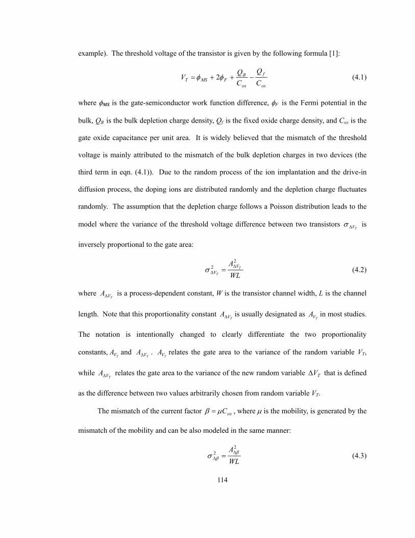
114
example). The threshold voltage of the transistor is given by the following formula [1]:
ox
f
ox
BFMST C
QCQ
V −++= φφ 2 (4.1)
where φMS is the gate-semiconductor work function difference, φF is the Fermi potential in the
bulk, QB is the bulk depletion charge density, Qf is the fixed oxide charge density, and Cox is the
gate oxide capacitance per unit area. It is widely believed that the mismatch of the threshold
voltage is mainly attributed to the mismatch of the bulk depletion charges in two devices (the
third term in eqn. (4.1)). Due to the random process of the ion implantation and the drive-in
diffusion process, the doping ions are distributed randomly and the depletion charge fluctuates
randomly. The assumption that the depletion charge follows a Poisson distribution leads to the
model where the variance of the threshold voltage difference between two transistors TV∆σ is
inversely proportional to the gate area:
WLA
T
T
VV
22 ∆∆ =σ (4.2)
where TVA∆ is a process-dependent constant, W is the transistor channel width, L is the channel
length. Note that this proportionality constant TVA∆ is usually designated as
TVA in most studies.
The notation is intentionally changed to clearly differentiate the two proportionality
constants,TVA and
TVA∆ . TVA relates the gate area to the variance of the random variable VT,
while TVA∆ relates the gate area to the variance of the new random variable TV∆ that is defined
as the difference between two values arbitrarily chosen from random variable VT.
The mismatch of the current factor oxCµβ = , where µ is the mobility, is generated by the
mismatch of the mobility and can be also modeled in the same manner:
WLA2
2 ββσ ∆
∆ = (4.3)

115
where β∆A is another process-dependent constant. In ref. [2], experiments were carried out
using pairs of transistors having various sizes and various mutual distances. For each transistor
pair that consists of two transistors of the identical dimension, VT and β are extracted form the
current measured in the linear region first, and then ∆VT and ∆ β are calculated as the difference
of the two parameters. Based on these measurement results, the above process-dependent
constants were determined.
In contrast to the above method where the current measurement was done in the linear
region, Bastos et al. have devised a new parameter extraction method which enables the current
measurement in the saturation region [3]. This method is advantageous especially for the
characterization in sub-micron processes where the resistance of the transistor in the linear
region becomes smaller, making the first method more prone to error due to the parasitic
resistance in the drain path. These experimental results are summarized in Table 4.1, which is
adapted from ref. [4] with the following modifications. The original notation TVA and βA are
replaced with TVA∆ and β∆A , respectively;
TVA and βA are newly calculated based on the
formula derived below and included in the table.
In these experiments, the influence of distance between two transistors on mismatch was
also investigated: the constants that relate the distance to the variation in the threshold voltage
and current factor were calculated. It was found that the influence of the distance is much
smaller than the influence of the gate area. Therefore, the influence of distance is not treated in
the following analysis. Another interesting finding which is commonly observed in these
experiments is that almost no correlation was found between TV∆ and β∆ . This finding
suggests that the gate oxide thickness is a well-controlled parameter with little variation since
these two variables (∆VT and ∆ β) have the term Cox in common.
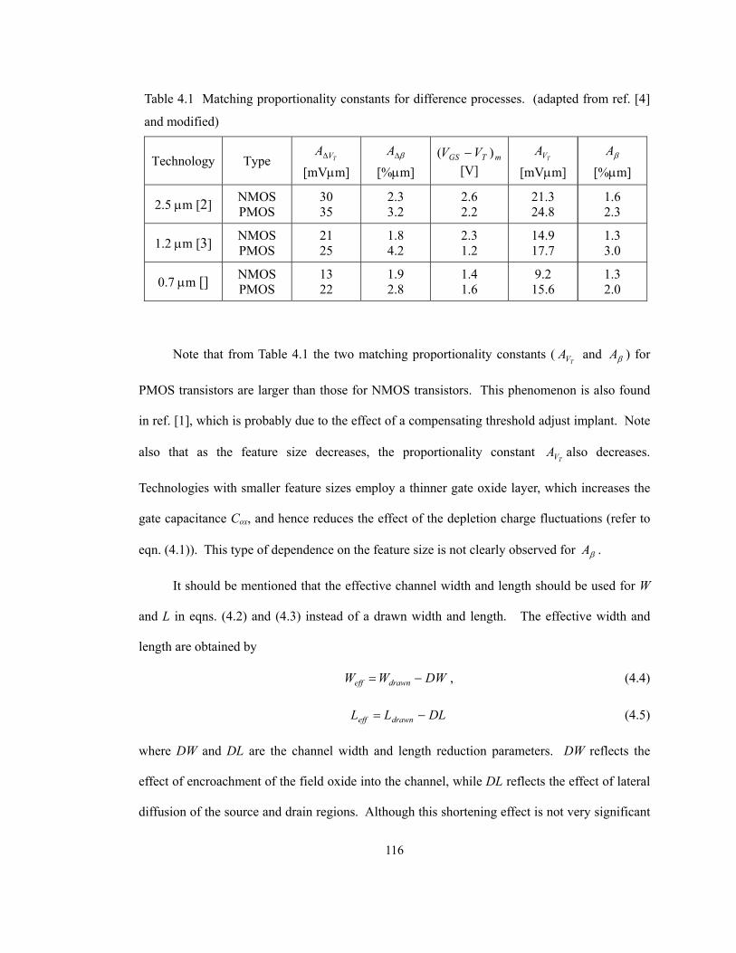
116
Note that from Table 4.1 the two matching proportionality constants (TVA and βA ) for
PMOS transistors are larger than those for NMOS transistors. This phenomenon is also found
in ref. [1], which is probably due to the effect of a compensating threshold adjust implant. Note
also that as the feature size decreases, the proportionality constant TVA also decreases.
Technologies with smaller feature sizes employ a thinner gate oxide layer, which increases the
gate capacitance Cox, and hence reduces the effect of the depletion charge fluctuations (refer to
eqn. (4.1)). This type of dependence on the feature size is not clearly observed for βA .
It should be mentioned that the effective channel width and length should be used for W
and L in eqns. (4.2) and (4.3) instead of a drawn width and length. The effective width and
length are obtained by
DWWW drawneff −= , (4.4)
DLLL drawneff −= (4.5)
where DW and DL are the channel width and length reduction parameters. DW reflects the
effect of encroachment of the field oxide into the channel, while DL reflects the effect of lateral
diffusion of the source and drain regions. Although this shortening effect is not very significant
Table 4.1 Matching proportionality constants for difference processes. (adapted from ref. [4]
and modified)
Technology Type TVA∆ [mVµm]
β∆A [%µm]
mTGS VV )( −[V]
TVA [mVµm]
βA [%µm]
2.5 µm [2] NMOS PMOS
30 35
2.3 3.2
2.6 2.2
21.3 24.8
1.6 2.3
1.2 µm [3] NMOS PMOS
21 25
1.8 4.2
2.3 1.2
14.9 17.7
1.3 3.0
0.7 µm [] NMOS PMOS
13 22
1.9 2.8
1.4 1.6
9.2 15.6
1.3 2.0
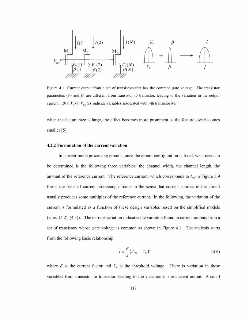
117
when the feature size is large, the effect becomes more prominent as the feature size becomes
smaller [5].
4.2.2 Formulation of the current variation
In current-mode processing circuits, once the circuit configuration is fixed, what needs to
be determined is the following three variables: the channel width, the channel length, the
amount of the reference current. The reference current, which corresponds to Iref in Figure 3.9
forms the basis of current processing circuits in the sense that current sources in the circuit
usually produces some multiples of the reference current. In the following, the variation of the
current is formulated as a function of these design variables based on the simplified models
(eqns. (4.2), (4.3)). The current variation indicates the variation found in current outputs from a
set of transistors whose gate voltage is common as shown in Figure 4.1. The analysis starts
from the following basic relationship:
( )2
2 TGS VVI −=β (4.6)
where β is the current factor and VT is the threshold voltage. There is variation in these
variables from transistor to transistor, leading to the variation in the current output. A small
GSVTV refIIβ
)1(I
)1(TV)1(β
)2(I
)2(TV)2(β
)(NI
)(NVT)(Nβ
TV β I
1M 2M NM
Figure 4.1 Current output from a set of transistors that has the common gate voltage. The transistor
parameters (VT and β) are different from transistor to transistor, leading to the variation in the output
current. )(),(),( iViVi GSTβ indicate variables associated with i-th transistor Mi.

118
difference in β and VT between two transistors generates a small difference in I. Let us consider
a pair of transistors M1 and M2 as a representative set and define the following variables:
)2()1( III −=∆ , (4.7)
)2()1( βββ −=∆ , (4.8)
)2()1( TTT VVV −=∆ , (4.9)
and
2
)2()1( III += , (4.10)
2
)2()1( βββ += , (4.11)
2
)2()1( TTT
VVV
+= . (4.12)
The small change in the current ∆I is represented as
TT
VVIII ∆
∂∂
+∆∂∂
=∆ ββ
. (4.13)
By calculating each derivative, we get
( ) ( ) TTGSTGS VVVVVI ∆−−∆−=∆ ββ2
21 . (4.14)
The following equation, which is a modified version of eqn. (4.6), is valid if higher order
terms are neglected:
( )2
2 TGS VVI −=β . (4.15)
By dividing eqn. (4.14) by (4.15), the representation for the relative change is expressed as
follows:
TGS
T
VVV
II
−
∆−
∆=
∆ 2ββ . (4.16)

119
Eqn. (4.16) is valid only for a pair of transistors and needs to be extended to explain the
overall statistics on the current variation for a large number of transistors. This is possible by
considering each variable in eqn. (4.16) as a random variable. Since it is experimentally
confirmed that there is almost no correlation between β and VT [2][3], hence no correlation
between ∆β and ∆VT, the relative variation of ∆I is represented as the summation of the relative
variation of ∆β and ∆VT:
222 2
−+
=
∆∆∆
TGS
VI
VVIT
σ
β
σσ β (4.17)
where TVI ,, β represents the mean of each variable for an entire set of transistors. In general,
for any random variable P, the variance of the difference of any two, which is defined as
∆ P = P1 - P2, is represented as
2222 2 PPPP σσσσ =+=∆ . (4.18)
Applying this identity for variables which appear in eqn. (4.17) yields
222 2
−+
=
TGS
VI
VVIT
σ
β
σσ β . (4.19)
This expression statistically relates the variation of β and VT to that of I for a large
number of transistors. Eqn. (4.18) can be applied to eqn. (4.2) to yield
WLA
T
T
VV
22 =σ (4.20)
where
2/TT VV AA ∆= (4.21)
is the mismatch proportionality constant which relates the variance of the threshold voltage to
the gate area. Likewise,

120
WLA2
2 ββσ = (4.22)
where
2/ββ ∆= AA . (4.23)
Substituting eqns. (4.20) and (4.22) into (4.19) yields
−+=
2
22 21
TGS
VI
VV
AA
WLIT
βσ
. (4.24)
Let us compare the first term with the second term to find out the relative importance of
each term. These two terms become equal when the transistor is biased such that:
βA
AVV TV
TGS
2=− . (4.25)
This voltage, which is termed as corner gate-drive voltage in ref. [4], is shown in the fifth
column in Table 4.1 as ( )mTGS VV − . If transistors are biased below this value, the contribution
of the second term in eqn. (4.24) is larger than the first term. The ratio of the second term to the
first term is given as
2
22
)(2
−
−=
− TGS
mTGS
TGS
V
VVVV
AVV
AT
β . (4.26)
As one of the typical examples, this ratio becomes 9 for ( )mTGS VV − equal to 1.5 [V] and
( )TGS VV − equal to 0.5 [V], which is large enough to neglect the effect of the first term in eqn.
(4.24). Therefore, eqn. (4.24) can be simplified as
22 21
−=
TGS
VI
VV
AWLI
Tσ. (4.27)
or equivalently
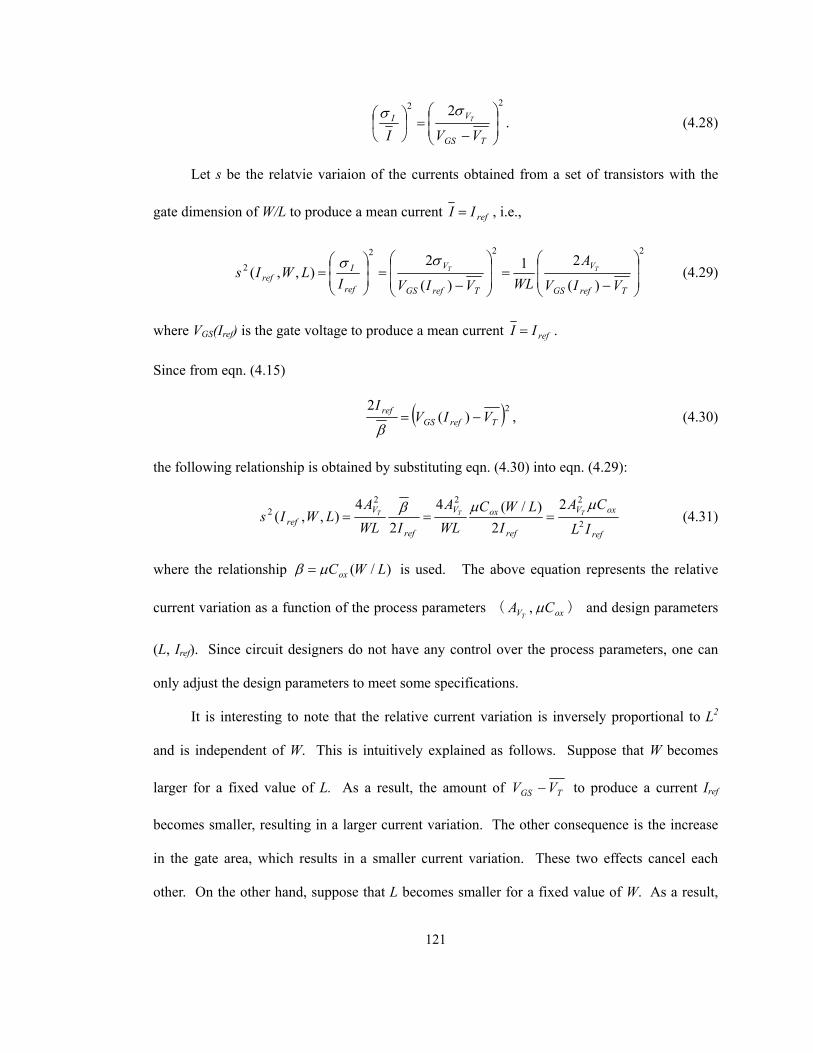
121
22 2
−=
TGS
VI
VVIT
σσ. (4.28)
Let s be the relatvie variaion of the currents obtained from a set of transistors with the
gate dimension of W/L to produce a mean current refII = , i.e.,
222
2
)(
21)(
2),,(
−=
−=
=
TrefGS
V
TrefGS
V
ref
Iref VIV
AWLVIVI
LWIs TTσσ
(4.29)
where VGS(Iref) is the gate voltage to produce a mean current refII = .
Since from eqn. (4.15)
( )2)(
2TrefGS
ref VIVI
−=β
, (4.30)
the following relationship is obtained by substituting eqn. (4.30) into eqn. (4.29):
ref
oxV
ref
oxV
ref
Vref IL
CAI
LWCWLA
IWLA
LWIs TTT
2
2222 2
2)/(4
24
),,(µµβ
=== (4.31)
where the relationship )/( LWCoxµβ = is used. The above equation represents the relative
current variation as a function of the process parameters ( oxV CAT
µ, ) and design parameters
(L, Iref). Since circuit designers do not have any control over the process parameters, one can
only adjust the design parameters to meet some specifications.
It is interesting to note that the relative current variation is inversely proportional to L2
and is independent of W. This is intuitively explained as follows. Suppose that W becomes
larger for a fixed value of L. As a result, the amount of TGS VV − to produce a current Iref
becomes smaller, resulting in a larger current variation. The other consequence is the increase
in the gate area, which results in a smaller current variation. These two effects cancel each
other. On the other hand, suppose that L becomes smaller for a fixed value of W. As a result,

122
the amount of TGS VV − to accommodate a current Iref becomes smaller and the gate area also
becomes smaller, both of which work to increase the current variation. This is why the current
variation is inversely proportional to the square of the channel length. To explicitly express the
above dependence, s is expressed as s(Iref , L) instead of s(Iref , W, L) hereafter. The current
variation σI in eqn. (4.29) can be also explicitly expressed as a function of Iref and L:
222 ),(),( refrefrefI ILIsLI =σ . (4.32)
Using eqn. (4.31), let us consider the relative current variation for the case where the
current level is mIref, and the channel length is bL. The relative current variation decreases by a
factor of mb2 since
( )
),(1212),( 2
22
2
22
22 LIs
mbIL
CA
mbmIbL
CAbLmIs ref
ref
oxV
ref
oxVref
TT ===µµ
. (4.33)
The variance of the current increases by a factor of m/b2 since
.),(),(
))(,(1)(),(),(
22
222
222
222
LIbmILIs
bm
mILIsmb
mIbLmIsbLmI
refIrefref
refrefrefrefrefI
σ
σ
==
== (4.34)
Hereafter, ),(2 LIs ref will be simply designated as s2 for simplicity since this term is frequently
used in the derivations described below.
4.2.3 Error introduced by current mirror
A formula for the current variation as a function of the design parameters is derived in the
previous subsection. The formula is extended to incorporate the effect of VGS variation to
represent the error, i.e., the increase of the variance of the current, by the current mirror
operation. Figure 4.2 shows the effect of VGS variation on the current variation. The difference
between Figure 4.2 and Figure 4.1 lies in the treatment of VGS, which is not a fixed parameter
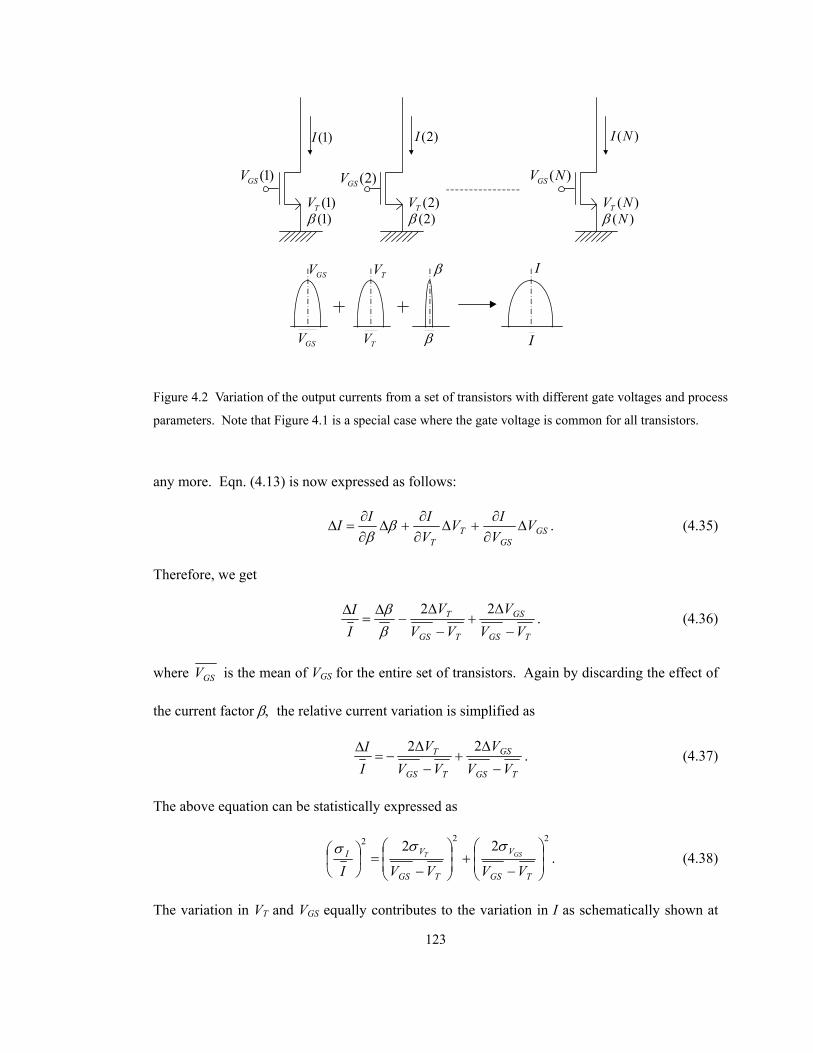
123
any more. Eqn. (4.13) is now expressed as follows:
GSGS
TT
VV
IVVIII ∆
∂∂
+∆∂∂
+∆∂∂
=∆ ββ
. (4.35)
Therefore, we get
TGS
GS
TGS
T
VVV
VVV
II
−
∆+
−
∆−
∆=
∆ 22ββ . (4.36)
where GSV is the mean of VGS for the entire set of transistors. Again by discarding the effect of
the current factor β, the relative current variation is simplified as
TGS
GS
TGS
T
VVV
VVV
II
−
∆+
−
∆−=
∆ 22. (4.37)
The above equation can be statistically expressed as
222 22
−+
−=
TGS
V
TGS
VI
VVVVIGST
σσσ. (4.38)
The variation in VT and VGS equally contributes to the variation in I as schematically shown at
)1(I
)1(TV)1(β
)2(I
)2(TV)2(β
)(NVGS
)(NI
)(NVT)(Nβ
TV refIIβGSV
)2(GSV)1(GSV
TV β IGSV
Figure 4.2 Variation of the output currents from a set of transistors with different gate voltages and process
parameters. Note that Figure 4.1 is a special case where the gate voltage is common for all transistors.
124
the bottom of Figure 4.2. Now let us formulate the error introduced by the current mirror circuit
based on the schematic shown in Figure 4.3. Eqn. (4.38) is modified to represent the relative
variation of the current I2 as
2
2
2
2
2
2
2222
−+
−=
TGS
V
TGS
VI
VVVVIGST
σσσ. (4.39)
In order to express the second term in the right-hand side as a function of the variation in the
input current I1 and the variation in the threshold voltage VT1, eqn. (4.37) is expressed in a
slightly different way:
.22
1
1
1 TGS
T
TGS
GS
VVV
II
VVV
−
∆+
∆=
−
∆ (4.40)
Eqn. (4.40) clearly explains that the variation in VGS is generated by the variation in I and VT,
which can be again statistically represented as
)1(1I
)1(2TV)1(GSV2M1M
)1(1TV
)1(2I )2(1I
)2(2TV)2(GSV2M1M
)2(1TV
)2(2I )(1 NI
)(2 NVT)(NVGS
2M1M)(1 NVT
)(2 NI
GSV
TV 2I
1I TV
GSV
1I 1TV GSV
GSV 2TV 2I
Figure 4.3 Schematic showing the increase of the current variation by current mirror operation.

125
2
1
2
11
1122
−+
=
− TGS
VI
TGS
V
VVIVVTGS
σσσ. (4.41)
By substituting eqn. (4.41) to (4.39), we get
2
2
2
1
2
1
2
2
211222
−+
−+
=
TGS
V
TGS
VII
VVVVIITT
σσσσ. (4.42)
Suppose that the mean input current for transistor M1 and the output current from
transistor M2 are
refref ImIba
I 11
11 == (4.43)
and
refref ImIba
I 22
22 == , (4.44)
respectively, with the corresponding transistor dimension of a1W/b1L for transistor M1 and
a2W/b2L for transistor M2. In the above expressions, m1=a1/b1 and m2 =a2/b2 represent the
current amplification coefficient. Substituting eqns. (4.43) and (4.44) into (4.42), we get
2222
2211
2
1
2
2
1112 sbm
sbmImIm ref
I
ref
I ++
=
σσ (4.45)
where eqns. (4.29) and (4.33) are used to obtain the second and the third term in the right-hand
side. It can be further modified as
22
22
22221
122
222
22222
2222
211
22
2
1
22
1
12
refrefI
refrefII
Isbm
Isbm
gg
Isbm
mIs
bmm
mm
++=
++
=
σ
σσ (4.46)
where g2 represents the current gain defined as m2/m1=I2/I1. The first term and the second term
represent the contribution of the variance of the input current and the variance of the threshold
126
voltage of transistor M1, respectively. Note that these contributions are magnified by the square
of the current gain. The third term represents the contribution of the variance of the threshold
voltage of transistor M2. Note that in the special case where transistor M1 and M2 have the same
gate dimension, i.e., a1=a2=a, b1=b2=b, and subsequently m1=m2=m=a/b, g2=1, eqn. (4.46) is
simplified as
222
22 212 refII Is
bm
+= σσ . (4.47)
4.2.4 Error introduced by current summation and subtraction
In addition to the current mirroring operation, current summation and subtraction are
extensively employed in current-mode processing circuits. Therefore, the effect of these
operations on the variation should be formulated. In general, for a random variable X, which is
defined as the summation or subtraction of X1, X2, … , XN, i.e.,
,...2211 NN XpXpXpX +++= (4.48)
where pi is either +1 or –1, the variance of X is expressed as
∑∑∑= ≠=
+=N
i
N
ijXXji
N
iXX jii
pp1
2
1
22 2 σσσ (4.49)
where 2ji XXσ is the covariance between two random variables Xi and Xj. Based on this formula,
two cases, a case where no correlation exists between currents and the other case where
correlation exists between currents, are analyzed below.
Figure 4.4 shows the example of the first case where no correlation exists between any
pair of current. The output current I3 is obtained as the summation of the three currents, I3a , I3b ,
and I3c . These three current outputs are generated from three sets of current mirror circuit.
Each of the input currents for these current mirror circuits, I1a , I1b , and I1c, has the variance of
22refIs . The variance of I1a , I1b , and I1c is calculated as
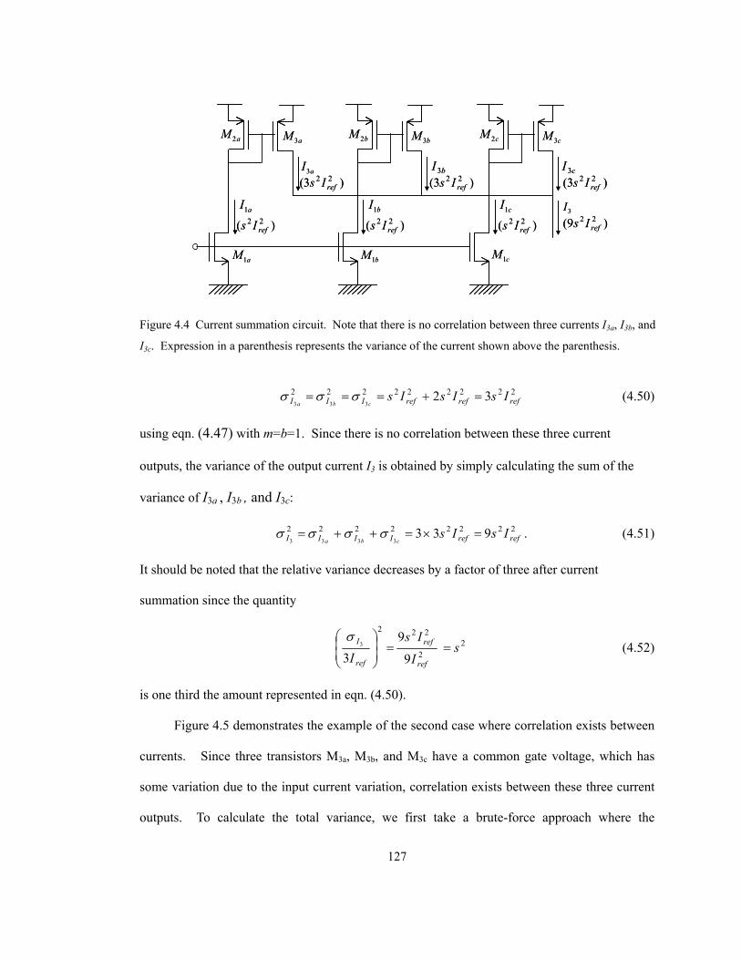
127
222222222 32333 refrefrefIII IsIsIs
cba=+=== σσσ (4.50)
using eqn. (4.47) with m=b=1. Since there is no correlation between these three current
outputs, the variance of the output current I3 is obtained by simply calculating the sum of the
variance of I3a , I3b , and I3c:
22222222 9333333 refrefIIII IsIs
cba=×=++= σσσσ . (4.51)
It should be noted that the relative variance decreases by a factor of three after current
summation since the quantity
22
222
9
93
3 sI
IsI ref
ref
ref
I ==
σ (4.52)
is one third the amount represented in eqn. (4.50).
Figure 4.5 demonstrates the example of the second case where correlation exists between
currents. Since three transistors M3a, M3b, and M3c have a common gate voltage, which has
some variation due to the input current variation, correlation exists between these three current
outputs. To calculate the total variance, we first take a brute-force approach where the
aM1
aM 2 aM 3
aI3
)3( 22refIs
bI3
bM 2 bM 3 cM 2 cM 3
bM1 cM1
aI1 3I
cI 3
)3( 22refIs )3( 22
refIs
)9( 22refIs)( 22
refIs )( 22refIs )( 22
refIsbI1 cI1
aM1
aM 2 aM 3
aI3
)3( 22refIs
bI3
bM 2 bM 3 cM 2 cM 3
bM1 cM1
aI1 3I
cI 3
)3( 22refIs )3( 22
refIs
)9( 22refIs)( 22
refIs )( 22refIs )( 22
refIsbI1 cI1
Figure 4.4 Current summation circuit. Note that there is no correlation between three currents I3a, I3b, and
I3c. Expression in a parenthesis represents the variance of the current shown above the parenthesis.
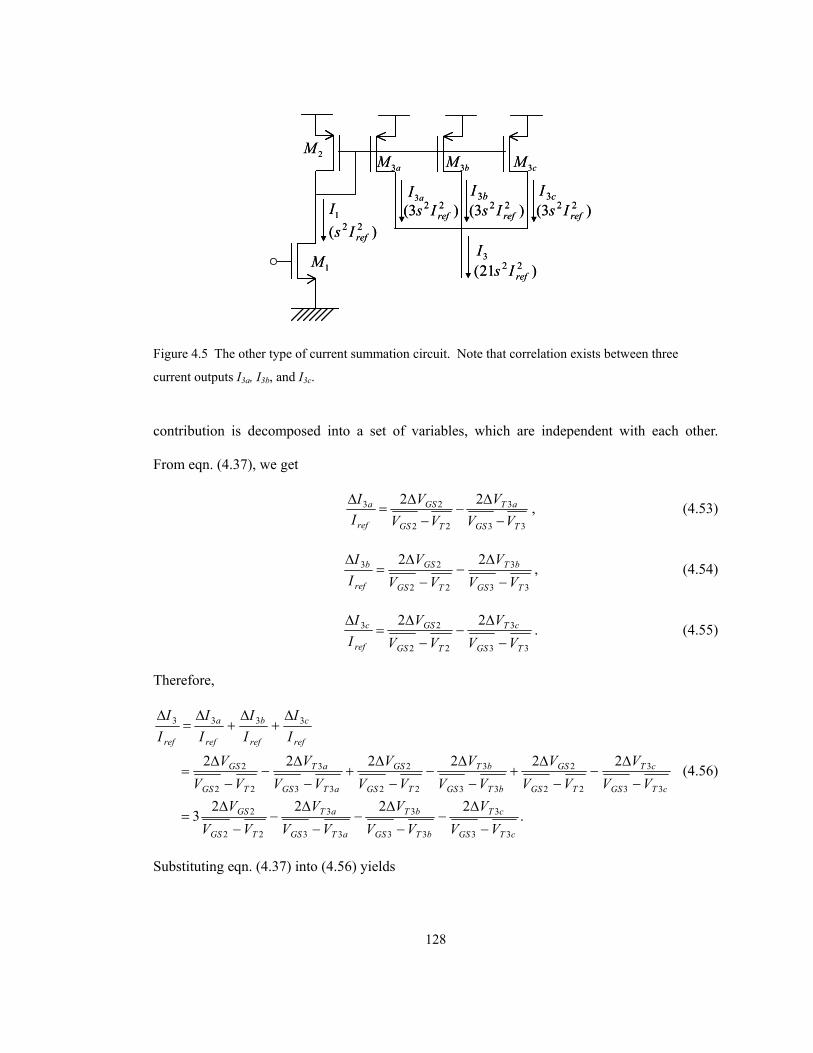
128
contribution is decomposed into a set of variables, which are independent with each other.
From eqn. (4.37), we get
33
3
22
23 22
TGS
aT
TGS
GS
ref
a
VVV
VVV
II
−∆
−−
∆=
∆ , (4.53)
33
3
22
23 22
TGS
bT
TGS
GS
ref
b
VVV
VVV
II
−
∆−
−
∆=
∆, (4.54)
33
3
22
23 22
TGS
cT
TGS
GS
ref
c
VVV
VVV
II
−
∆−
−
∆=
∆. (4.55)
Therefore,
.2222
3
222222
33
3
33
3
33
3
22
2
33
3
22
2
33
3
22
2
33
3
22
2
3333
cTGS
cT
bTGS
bT
aTGS
aT
TGS
GS
cTGS
cT
TGS
GS
bTGS
bT
TGS
GS
aTGS
aT
TGS
GS
ref
c
ref
b
ref
a
ref
VVV
VVV
VVV
VVV
VVV
VVV
VVV
VVV
VVV
VVV
II
II
II
II
−
∆−
−
∆−
−
∆−
−
∆=
−
∆−
−
∆+
−
∆−
−
∆+
−
∆−
−
∆=
∆+
∆+
∆=
∆
(4.56)
Substituting eqn. (4.37) into (4.56) yields
1I
1M
2MaM 3 bM 3 cM 3
aI3
3I)( 22
refIs
bI 3 cI 3)3( 22
refIs )3( 22refIs )3( 22
refIs
)21( 22refIs
1I
1M
2MaM 3 bM 3 cM 3
aI3
3I)( 22
refIs
bI 3 cI 3)3( 22
refIs )3( 22refIs )3( 22
refIs
)21( 22refIs
Figure 4.5 The other type of current summation circuit. Note that correlation exists between three
current outputs I3a, I3b, and I3c.
129
cTGS
cT
bTGS
bT
aTGS
aT
TGS
T
ref VVV
VVV
VVV
VVV
II
II
33
3
33
3
33
3
22
2
1
13 22223
−
∆−
−
∆−
−
∆−
−
∆+
∆=
∆, (4.57)
which further leads to
cTGS
cT
bTGS
bT
aTGS
aT
TGS
T
TGS
T
ref VVV
VVV
VVV
VVV
VVV
II
33
3
33
3
33
3
22
2
11
13 222223
−
∆−
−
∆−
−
∆−
−
∆+
−
∆−=
∆ (4.58)
by using eqn. (4.37) with ∆VGS=0 since the gate voltage of transistor M1 is fixed. Now the
above equation represents the current variation as a total contribution of the variation of each
threshold voltage with different weigths, i.e., heigher contribution from transistors M1 and M2,
and lower contribution from transistors M3a, M3b, and M3c. Since there is no correlation
between these random variables, the variation in ∆I3 /Iref is represented as the summation of the
variance of each variable:
.222
29
29
2
33
2
33
2
33
2
22
2
11
2
333
213
−+
−+
−+
−+
−=
∆∆∆
∆∆∆
cTGS
V
bTGS
V
aTGS
V
TGS
V
TGS
V
ref
I
VVVVVV
VVVVI
cTbTaT
TT
σσσ
σσσ
(4.59)
Using eqn. (4.18), we get
2
22222
2
33
2
33
2
33
2
22
2
11
2
21
99
222
29
29
333
213
s
sssss
VVVVVV
VVVVI
cTGS
V
bTGS
V
aTGS
V
TGS
V
TGS
V
ref
I
cTbTaT
TT
=
++++=
−+
−+
−+
−+
−=
σσσ
σσσ
(4.60)
or equivalently
222 213 refI Is=σ . (4.61)
The variance is more than twice that described in eqn. (4.51) due to the presence of the
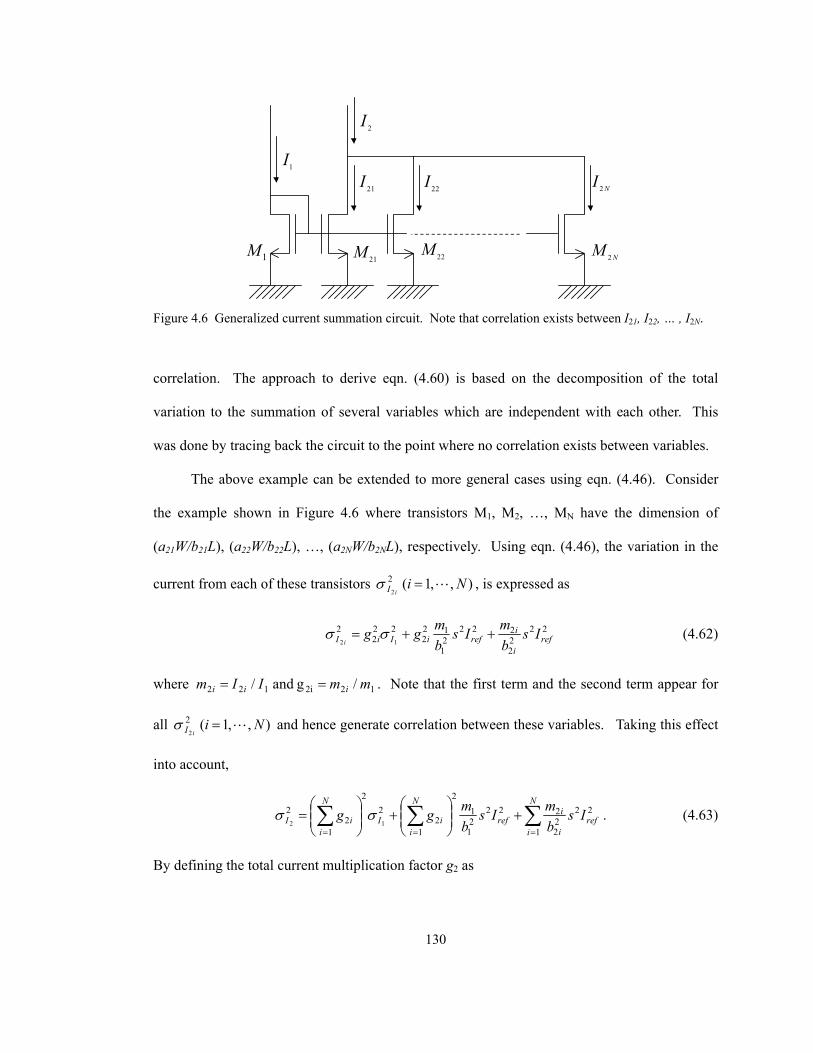
130
correlation. The approach to derive eqn. (4.60) is based on the decomposition of the total
variation to the summation of several variables which are independent with each other. This
was done by tracing back the circuit to the point where no correlation exists between variables.
The above example can be extended to more general cases using eqn. (4.46). Consider
the example shown in Figure 4.6 where transistors M1, M2, …, MN have the dimension of
(a21W/b21L), (a22W/b22L), …, (a2NW/b2NL), respectively. Using eqn. (4.46), the variation in the
current from each of these transistors ),,1(22
NiiI L=σ , is expressed as
2222
22221
122
222
212 ref
i
irefiIiI Is
bmIs
bmgg
i++= σσ (4.62)
where 122i122 /g and / mmIIm iii == . Note that the first term and the second term appear for
all ),,1(22
NiiI L=σ and hence generate correlation between these variables. Taking this effect
into account,
∑∑∑===
+
+
=
N
iref
i
iref
N
iiI
N
iiI Is
bmIs
bmgg
1
2222
2222
1
12
12
22
12
212
σσ . (4.63)
By defining the total current multiplication factor g2 as
1I
1M21M
21I 22I NI 2
22MNM 2
2I
Figure 4.6 Generalized current summation circuit. Note that correlation exists between I21, I22, … , I2N.

131
∑=
=N
iigg
122 , (4.64)
eqn. (4.63) can be simply represented as
∑=
++=N
iref
i
irefII Is
bm
Isbm
gg1
2222
2222
1
122
222
212
σσ . (4.65)
A set of transistors M2i act as a lumped one big transistor having a current gain of g2 with
respect to transistor M1, which magnifies the variance prior to M2i, i.e., variance in the input
current I1 and the threshold voltage of transistor M1. On the other hand, the variance of the
threshold voltage of each transistor M2i is independent with each other, and hence just adds up
without generating the cross term due to the correlation effect. Note that the result shown in
(4.60) is immediately obtained by substituting 3 for g2, 22refIs for 2
1Iσ and setting other
variables to 1.
The approach described so far to calculate the total variance is based on the
decomposition of the variance of each current into the sum of the variance of the threshold
voltage of each transistor which exists prior to the current summation stage. In this way, the
effect of correlation can be clearly observed.
To summarize this section, the three useful formulas have been derived starting from the
model that characterize transistor mismatch:
(1) The relative current variation of the transistor is a function of L and Iref. Larger values of L
and Iref give smaller variations (eqn. (4.31)).
(2) Current mirror operation increases variation by 222 )/(2 refIsbm , equally contributed from
two transistors used in a pair, where s2 is defined as the current variation due to the threshold
mismatch for current Iref (eqn. (4.47)).
(3) The variance of the current which is represented as summation of multiple input currents is

132
obtained by simply adding the variance of each current. The variance becomes larger when
there is correlation between these currents.
4.3 Systematic design procedure for current-mode processing circuits
Based on the formulas derived in the previous section, a method to systematically design
a circuit is discussed in this section. To be more specific, the design parameters including the
reference current, the channel width and length, are determined to satisfy accuracy and speed
requirement while ensuring the operation in the correct operating region.
4.3.1 Background
Few papers have been published on a design procedure that takes transistor mismatch into
account. In his paper dealing with transistor mismatch [1], Lakshmikumar et al. have presented
a method for determining required accuracy for current sources in order to satisfy a specific
yield for an 8-bit current-steering CMOS DAC. The procedure is briefly described below as an
introduction of a systematic design procedure.
The output of the current-steering type DAC is generated by the selective summation of
the eight current sources whose current level is represented as )8,,1(2 L=iI uniti where Iunit is
a unit current amount. The selection of the current source is controlled by the input word. The
authors have linked the linearity error of the DAC output to the random variation of the current,
and based on this link, represented the circuit yield as a function of the matching accuracy. In
other words, the required matching accuracy can be determined to satisfy a given yield
requirement. The nonlinearity of the output is expressed as the following normalized form:
yx
xz+
= (4.66)
where z is the normalized output, and x and y are the output of the DAC for a given input word
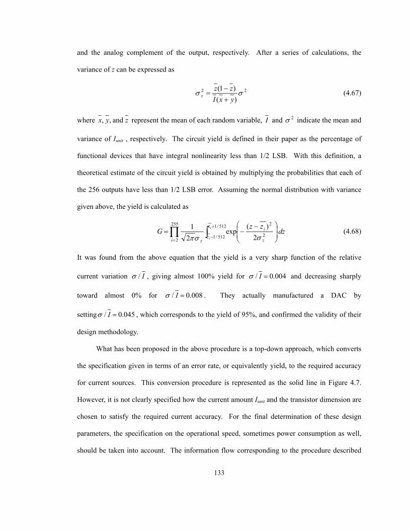
133
and the analog complement of the output, respectively. After a series of calculations, the
variance of z can be expressed as
22
)()1( σσ
yxIzz
z+−
= (4.67)
where zyx and,, represent the mean of each random variable, I and 2σ indicate the mean and
variance of Iunit , respectively. The circuit yield is defined in their paper as the percentage of
functional devices that have integral nonlinearity less than 1/2 LSB. With this definition, a
theoretical estimate of the circuit yield is obtained by multiplying the probabilities that each of
the 256 outputs have less than 1/2 LSB error. Assuming the normal distribution with variance
given above, the yield is calculated as
dzzz
G i
i
z
zz
i
i z∫∏
+
−=
−−=
512/1
512/1 2
2255
2 2)(
exp2
1σσπ
(4.68)
It was found from the above equation that the yield is a very sharp function of the relative
current variation I/σ , giving almost 100% yield for 004.0/ =Iσ and decreasing sharply
toward almost 0% for 008.0/ =Iσ . They actually manufactured a DAC by
setting 045.0/ =Iσ , which corresponds to the yield of 95%, and confirmed the validity of their
design methodology.
What has been proposed in the above procedure is a top-down approach, which converts
the specification given in terms of an error rate, or equivalently yield, to the required accuracy
for current sources. This conversion procedure is represented as the solid line in Figure 4.7.
However, it is not clearly specified how the current amount Iunit and the transistor dimension are
chosen to satisfy the required current accuracy. For the final determination of these design
parameters, the specification on the operational speed, sometimes power consumption as well,
should be taken into account. The information flow corresponding to the procedure described

134
above is schematically shown as two dashed lines in Figure 4.7. Starting from the next
subsection, the design procedure incorporating all these three lines of information flow is
described in detail.
4.3.2 Relationship between error rate and design parameters
In this subsection, the procedure to determine the maximum allowable current variation
to satisfy the specification given in terms of the error rate is described. This procedure
corresponds to the flow shown as the solid line in Figure 4.7, and has some similarity to
Lakshmikumar’s method described before in terms of analyzing the circuit behavior from the
point of a random process. Let us analyze the circuit shown in Figure 4.8, which is an extracted
part of the pixel circuit designed prior to that shown in Figure 3.9. Each of the three sets of
current-sourcing PMOS transistors and each of the three sets of current-sinking NMOS
transistors corresponds to one of the neighboring pixels.
Note that the current thresholding scheme is slightly different from the one shown in
Figure 3.9. The current summation result I4 is mirrored to I5 to be compared to the thresholding
current designated as Ith. The operation analyzed below is the detection of o45 line segments,
which is described in Chapter 2 The template consists of three 1's at the right diagonal position,
three –1’s at the upper triangle or the lower triangle, and three 0’s at the other side of triangle.
specification 1:error rate (yield)
required current accuracy
determination of design parameters (W,L,I)
specification 2:speed (power)
1
2a
2b
Figure 4.7 Schematic explaining the design flow of the systematic circuit design.
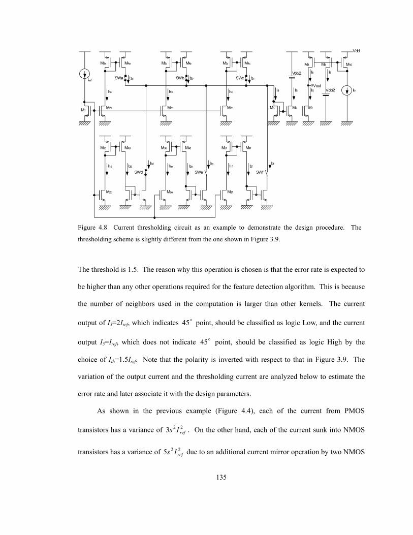
135
The threshold is 1.5. The reason why this operation is chosen is that the error rate is expected to
be higher than any other operations required for the feature detection algorithm. This is because
the number of neighbors used in the computation is larger than other kernels. The current
output of I5=2Iref, which indicates o45 point, should be classified as logic Low, and the current
output I5=Iref, which does not indicate o45 point, should be classified as logic High by the
choice of Ith=1.5Iref. Note that the polarity is inverted with respect to that in Figure 3.9. The
variation of the output current and the thresholding current are analyzed below to estimate the
error rate and later associate it with the design parameters.
As shown in the previous example (Figure 4.4), each of the current from PMOS
transistors has a variance of 223 refIs . On the other hand, each of the current sunk into NMOS
transistors has a variance of 225 refIs due to an additional current mirror operation by two NMOS
M1M2a
M3a M4a
I2a I2b I2c
M3b M4b M3c M4c
M2b M2c
I1bI1a I1c
Vout
M5 M6 M7
M8 M9 M10
I5
Vdd/2
Vdd/2
I6
Iref
Ith
Vdd
SWcSWbSWa
M2d
M3d M4d
M2e
M3e M4d
M2f
M3f M4f
I3d I3e I3fI1d I2d I1e I2e I1f I2f
I4
SWd SWe SWf
I5
I6
Figure 4.8 Current thresholding circuit as an example to demonstrate the design procedure. The
thresholding scheme is slightly different from the one shown in Figure 3.9.

136
transistors. Two cases are analyzed below to calculate the variance of I5 and Ith. In the first
case, the pixel is categorized as o45 by the presence of three 1’s and one –1, corresponding to
the output current of 2Iref. The variance of current I4 is )533(14 222 sss +×= . This current is
next mirrored to produce output current I5. This current mirror operation increases the current
variance by )22(4 2222refref IsIs ×= since the current level is 2Iref (refer to eqn. (4.47) with m=2
and b=1), which results in the variance of I5 equal to 2218 refIs .
In the second case, the pixel is not categorized as o45 by the presence of three 1’s and
two –1’s, corresponding to the output current of Iref. The variance of the output current I4 is
calculated as )5233(19 222 sss ×+×= . The subsequent current mirror operation increases the
current variance by 2s2, which results in the variance of I5 equal to 21s2. On the other hand, the
variation of the threshold current is 225.1 refIs .
Although so far no assumption has been made on the shape of the probability distribution,
the Gaussian distribution is assumed for generality and analytical simplicity. Hence,
hereinafter, the above three distributions are desiganted as
),18,2()( 222 refref IsINxp = (4.69)
)21,()( 221 refref IsINxp = , (4.70)
and
),5.1,5.1()( 225.1 refref IsINxp = (4.71)
respectively, where ),( 2σmN is the Gaussian distribution with the mean value m and the
variance σ2. The distributions for different values of s (s=0.03 and s=0.05) are shown in Figure
4.9. Note that the x-axis is scaled to Iref . For s=0.03, which is shown on the left-hand side, the
probability distribution is not very broad and almost no overlap exists between p1(x) and p1.5(x),
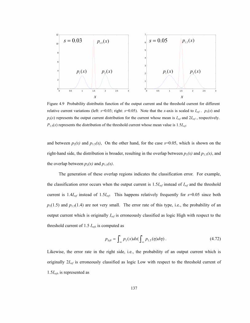
137
and between p2(x) and p1.5(x), On the other hand, for the case s=0.05, which is shown on the
right-hand side, the distribution is broader, resulting in the overlap between p1(x) and p1.5(x), and
the overlap between p2(x) and p1.5(x).
The generation of these overlap regions indicates the classification error. For example,
the classification error occurs when the output current is 1.5Iref instead of Iref and the threshold
current is 1.4Iref instead of 1.5Iref. This happens relatively frequently for s=0.05 since both
p1(1.5) and p1.5(1.4) are not very small. The error rate of this type, i.e., the probability of an
output current which is originally Iref is erroneously classified as logic High with respect to the
threshold current of 1.5 Iref, is computed as
))(()( 5.11 ∫∫ ∞−
∞
∞−=
x
left dpdxxpp ηη . (4.72)
Likewise, the error rate in the right side, i.e., the probability of an output current which is
originally 2Iref is erroneously classified as logic Low with respect to the threshold current of
1.5Iref, is represented as
0 0.5 1 1.5 2 2.5 30
2
4
6
8
10
12
0 0.5 1 1.5 2 2.5 30
1
2
3
4
5
6
7
)(1 xp
)(5.1 xp
)(2 xp
)(5.1 xp
)(2 xp)(1 xp
03.0=s 05.0=s
x xFigure 4.9 Probability distributin function of the output current and the threshold current for different
relative current variations (left: s=0.03; right: s=0.05). Note that the x-axis is scaled to Iref . p1(x) and
p2(x) represents the output current distribution for the current whose mean is Iref and 2Iref , respectively.
P1.5(x) represents the distribution of the threshold current whose mean value is 1.5Iref.
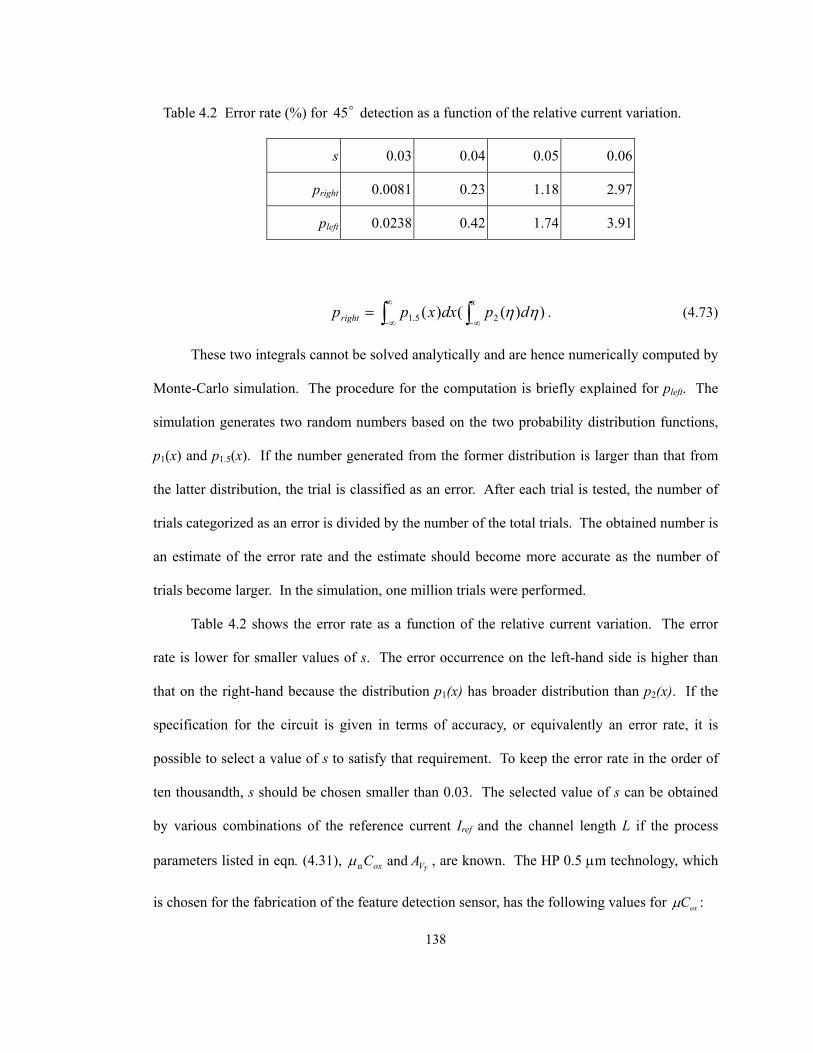
138
))(()( 25.1 ∫∫ ∞−
∞
∞−=
x
right dpdxxpp ηη . (4.73)
These two integrals cannot be solved analytically and are hence numerically computed by
Monte-Carlo simulation. The procedure for the computation is briefly explained for pleft. The
simulation generates two random numbers based on the two probability distribution functions,
p1(x) and p1.5(x). If the number generated from the former distribution is larger than that from
the latter distribution, the trial is classified as an error. After each trial is tested, the number of
trials categorized as an error is divided by the number of the total trials. The obtained number is
an estimate of the error rate and the estimate should become more accurate as the number of
trials become larger. In the simulation, one million trials were performed.
Table 4.2 shows the error rate as a function of the relative current variation. The error
rate is lower for smaller values of s. The error occurrence on the left-hand side is higher than
that on the right-hand because the distribution p1(x) has broader distribution than p2(x). If the
specification for the circuit is given in terms of accuracy, or equivalently an error rate, it is
possible to select a value of s to satisfy that requirement. To keep the error rate in the order of
ten thousandth, s should be chosen smaller than 0.03. The selected value of s can be obtained
by various combinations of the reference current Iref and the channel length L if the process
parameters listed in eqn. (4.31), TVox AC andnµ , are known. The HP 0.5 µm technology, which
is chosen for the fabrication of the feature detection sensor, has the following values for oxCµ :
Table 4.2 Error rate (%) for o45 detection as a function of the relative current variation.
s 0.03 0.04 0.05 0.06
pright 0.0081 0.23 1.18 2.97
pleft 0.0238 0.42 1.74 3.91

139
104=oxnCµ [µA/V2] (4.74)
and
35=oxpCµ [µA/V2] (4.75)
where suffixes n and p indicate that the parameter is for NMOS transistors and PMOS
transistors, respectively.
The other parameter required for the calculation of the design parameters, the mismatch
proportionality constant TVA , should be experimentally obtained from a test chip which
includes a lot of transistors of different gate areas. For the present design, however, this
proportionality constant TVA is estimated as 15 [mVµm] for both NMOS and PMOS transistors.
This is probably a rather conservative estimate considering experimentally obtained values of
TVA listed in Table 4.1. Table 4.3 shows the channel length for different values of s and
different values of Iref obtained by substituting those values listed in eqns. (4.74) and (4.75), and
m]mV[15 µ=TVA into eqn. (4.31). Numbers shown prior to the parenthesis is the calculated
value of L; numbers shown in the parenthesis is the drawn dimension. Larger values of L and
Iref are required to obtain smaller values of s, or equivalently, higher accuracy. The constraint at
this point for L and Iref is given in the product form of L2Iref. How to choose the optimal
combination of L and Iref is explained in the next section.
Before moving onto that topic, it is worth confirming by simulation that these obtained
values of L and Iref really produce the error as expected. A Monte-Carlo simulation was done
using Hspice circuit simulator in the following way. For each transistor in the circuit, the
threshold voltage was randomly chosen so that the overall distribution for the entire set of
transistors follow the normal distribution with its mean equal to the threshold voltage provided
by the vendor (HP) and with its variance equal to WLATV /2 . Simulations were performed ten

140
thousand times. Figure 4.10 shows the simulation result for different values of the channel
length (L) and the channel width (W). The reference current Iref is set to 1 µA. The two graphs
at the top display the effect of L on the error rate. The left graph and the right graph correspond
to the error rate pleft and pright, respectively. For both cases, the error rate decreases as the
channel length increases as is expected from Table 4.2 (shown as a dashed line).
On the other hand, the two graphs at the bottom, where the simulation results are re-
plotted as a function of W for different values of L, demonstrate that the influence of W on the
error rate is much smaller than the channel length. There is, however, a slight dependence of
the error rate on W especially when L is small possibly for the following reason. For larger
values of W/L, eqn. (4.6) is valid for larger current levels. In other words, for a current level of
1 µA, the relationship between TGS VV − and I is not as strong as specified in eqn. (3.6),
indicating an exponent smaller than 2. In this case, the proportionality constant relating
( )( )2/ TGSV VVT
−σ to ( )2/ IIσ in eqn. (4.19) becomes smaller than )2(4 2= , which leads to a
smaller current variation and hence a smaller error rate.
The simulation results shown above demonstrate the validity of the proposed design
procedure which converts the initial requirement for the error rate to the requirement for the
relative current accuracy and subsequently to the requirement for the design variables. The
Table 4.3 Channel lengths to satisfy the specified accuracy s for different values of Iref.
s 0.03 0.04 0.05 0.06
Ln [µm] 7.2 (7.3) 5.4 (5.5) 4.3 (4.4) 3.6 (3.7) Iref=1 [µA]
Lp [µm] 4.2 (4.3) 3.1 (3.2) 2.5 (2.6) 2.1 (2.2)
Ln [µm] 3.6 (3.7) 2.7 (2.8) 2.2 (2.3) 1.8 (1.9) Iref=4 [µA]
Lp [µm] 2.1 (2.2) 1.6 (1.7) 1.3 (1.4) 1.1 (1.2)
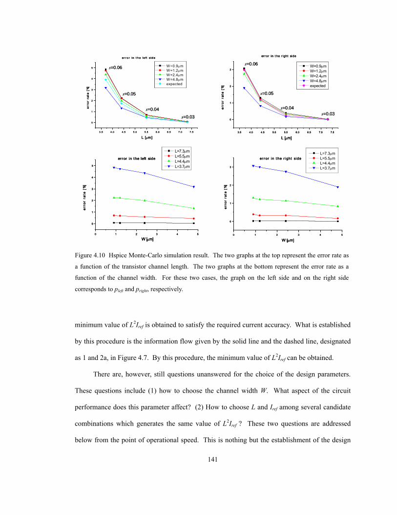
141
minimum value of L2Iref is obtained to satisfy the required current accuracy. What is established
by this procedure is the information flow given by the solid line and the dashed line, designated
as 1 and 2a, in Figure 4.7. By this procedure, the minimum value of L2Iref can be obtained.
There are, however, still questions unanswered for the choice of the design parameters.
These questions include (1) how to choose the channel width W. What aspect of the circuit
performance does this parameter affect? (2) How to choose L and Iref among several candidate
combinations which generates the same value of L2Iref ? These two questions are addressed
below from the point of operational speed. This is nothing but the establishment of the design
s=0.06
s=0.05
s=0.04
s=0.03
s=0.06
s=0.05
s=0.04s=0.03
3.5 4.0 4.5 5.0 5.5 6.0 6.5 7.0 7.5
0
1
2
3
L [µm]
er ror in t he r ight side
W=0.9µm W=1.2µm W=2.4µm W=4.8µm expected
erro
r ra
te [
%]
3 .5 4 .0 4 .5 5 .0 5 .5 6 .0 6 .5 7 .0 7 .5
0
1
2
3
4
5
L [µm]
er r o r i n t h e le ft s id e
W=0.9µm W=1.2µm W=2.4µm W=4.8µm expected
erro
r ra
te [
%]
0 1 2 3 4 5
0
1
2
3
er r or in t he r ight side L=7.3µm L=5.5µm L=4.4µm L=3.7µm
erro
r ra
te [
%]
W [µm]0 1 2 3 4 5
0
1
2
3
4
5
W [µm]
error in t he left side
L=7.3µm L=5.5µm L=4.4µm L=3.7µm
erro
r ra
te [
%]
s=0.06
s=0.05
s=0.04
s=0.03
s=0.06
s=0.05
s=0.04s=0.03
3.5 4.0 4.5 5.0 5.5 6.0 6.5 7.0 7.5
0
1
2
3
L [µm]
er ror in t he r ight side
W=0.9µm W=1.2µm W=2.4µm W=4.8µm expected
erro
r ra
te [
%]
3 .5 4 .0 4 .5 5 .0 5 .5 6 .0 6 .5 7 .0 7 .5
0
1
2
3
4
5
L [µm]
er r o r i n t h e le ft s id e
W=0.9µm W=1.2µm W=2.4µm W=4.8µm expected
erro
r ra
te [
%]
0 1 2 3 4 5
0
1
2
3
er r or in t he r ight side L=7.3µm L=5.5µm L=4.4µm L=3.7µm
erro
r ra
te [
%]
W [µm]0 1 2 3 4 5
0
1
2
3
4
5
W [µm]
error in t he left side
L=7.3µm L=5.5µm L=4.4µm L=3.7µm
erro
r ra
te [
%]
3 .5 4.0 4.5 5.0 5.5 6.0 6.5 7.0 7.5
0
1
2
3
L [µm]
er ror in t he r ight side
W=0.9µm W=1.2µm W=2.4µm W=4.8µm expected
erro
r ra
te [
%]
3 .5 4 .0 4 .5 5 .0 5 .5 6 .0 6 .5 7 .0 7 .5
0
1
2
3
4
5
L [µm]
er r o r i n t h e le ft s id e
W=0.9µm W=1.2µm W=2.4µm W=4.8µm expected
erro
r ra
te [
%]
0 1 2 3 4 5
0
1
2
3
er r or in t he r ight side L=7.3µm L=5.5µm L=4.4µm L=3.7µm
erro
r ra
te [
%]
W [µm]0 1 2 3 4 5
0
1
2
3
4
5
W [µm]
error in t he left side
L=7.3µm L=5.5µm L=4.4µm L=3.7µm
erro
r ra
te [
%]
Figure 4.10 Hspice Monte-Carlo simulation result. The two graphs at the top represent the error rate as
a function of the transistor channel length. The two graphs at the bottom represent the error rate as a
function of the channel width. For these two cases, the graph on the left side and on the right side
corresponds to pleft and pright, respectively.
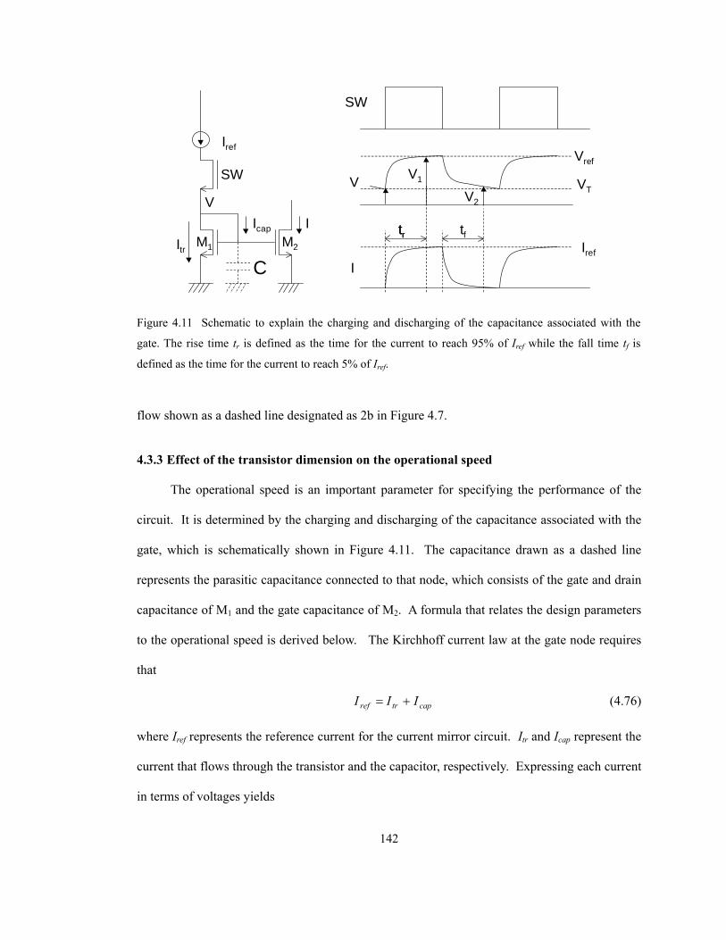
142
flow shown as a dashed line designated as 2b in Figure 4.7.
4.3.3 Effect of the transistor dimension on the operational speed
The operational speed is an important parameter for specifying the performance of the
circuit. It is determined by the charging and discharging of the capacitance associated with the
gate, which is schematically shown in Figure 4.11. The capacitance drawn as a dashed line
represents the parasitic capacitance connected to that node, which consists of the gate and drain
capacitance of M1 and the gate capacitance of M2. A formula that relates the design parameters
to the operational speed is derived below. The Kirchhoff current law at the gate node requires
that
captrref III += (4.76)
where Iref represents the reference current for the current mirror circuit. Itr and Icap represent the
current that flows through the transistor and the capacitor, respectively. Expressing each current
in terms of voltages yields
SW
V
I
tr tfIref
VT
tr
C
SW
V
Itr
Icap I
Vref
V1
V2
M1 M2
Iref
Figure 4.11 Schematic to explain the charging and discharging of the capacitance associated with the
gate. The rise time tr is defined as the time for the current to reach 95% of Iref while the fall time tf is
defined as the time for the current to reach 5% of Iref.

143
dtdVCVVVV TTref +−=− 22 )(
2)(
2ββ (4.77)
where Vref represents the gate voltage required to generate the current Iref . The above equation
can be further simplified to
dtdVCVVVV TTref =−−− ))()((
222β (4.78)
or equivalently
))(2(2 VVVVV
dVdtC refTref −−+
=β . (4.79)
Let us define the rise time tr as the time required for the current to reach I1=α Iref , and the
voltage V1 as the voltage which produces the current I1. V1 is obtained as
Tref VVV )1(1 αα −+=
by solving the following equation:
2211 )(
2)(
2 TrefT VVVVI −=−=βαβ . (4.80)
Then integrating the left-hand side of eqn. (4.79) from time 0 to tr and integrating the right-hand
side from VT to V1 yields
∫∫ −−+=
1
))(2(20
V
V refTref
Pt
T
r
VVVVVdVdt
Cβ . (4.81)
Using the following identity:
−+
−+−=
−−+ )(1
)2(1
)(21
))(2(1
VVVVVVVVVVVV refTrefTrefrefTref, (4.82)
Eqn. (4.81) is rewritten as
P
V
V refTrefTrefr dV
VVVVVVVt
C T∫
−+
−+−=
1 12
1)(2
12β . (4.83)

144
Substituting V1 into eqn. (4.83) and performing integration yields
Tref
T
VV
Vref
Tref
Trefr VV
VVVVV
tC
)1(2
ln)(2
12
ααβ
−+
−
−+
−= . (4.84)
By calculating the right-hand side, the rise time is obtained as
αα
β −
+−
=11ln
)( Trefr VV
Ct (4.85)
or alternatively
αα
β −
+=
11ln
2 refr
ICt . (4.86)
The fall time can be obtained almost in the same manner. Since Iref=0 in this case, eqn. (4.76)
reduces to
dtdVCVV T +−= 2)(
20 β (4.87)
or
2)(2 TVVdVdt
C −=
− β . (4.88)
Integrating the left-hand side from 0 to tf and integrating the right-hand side from Vref to V2
yields
212
V
VTf
refVV
Ct−
=β
(4.89)
where tf is defined as the fall time required for the current to decrease to I2=εIref , V2 is defined as
the gate voltage that produces the current I2, which is calculated as
Tref VVV )1(2 εε −+= . (4.90)
Substituting eqn. (4.90) into eqn. (4.89) gives

145
ε
εβ
)1(2)(
−−
=Tref
f VVCt (4.91)
or alternatively
ε
εβ
)1(22
−=
reff
ICt . (4.92)
Both eqns. (4.86) and (4.92) have the following term in common:
LIWLC
ILWC
WLC
IC
ref
ox
refox
ox
ref µµβ 98
)/(2322
2=
×= , (4.93)
which clearly demonstrates the effect of the design parameters on the rise time and the fall time.
Larger values of W and L contribute to larger values of the rise time and the fall time. Smaller
values of W are preferable for faster operation. However, L should be chosen carefully since
smaller values of L lead to faster operation as well as to lower accuracy (see eqn. (4.31)).
The relationship between the reference current and the channel length to satisfy the
accuracy and speed requirement is plotted in Figure 4.12. Note that the fall time is used as a
measure for specifying the operational speed. It is because the fall time is larger than the rise
time9 under the condition α =0.95 and ε=0.05. The channel width is set to 1.5 µm (5λ) instead
of the minimum dimension of 0.9 µm (3λ). The reason of this choice is based on the
information obtained from MOSIS for the AMI ABN technology, which says that the analog
designs using the scalable CMOS rules for the AMI SCMOS 1.2 µm (λ = 0.6 µm) run should
have a minimum channel width of 5λ and a minimum channel length of 3λ. Transistors with
the minimum W and minimum L are not being rendered with sufficiently stable characteristics
for analog circuit designs. Although the target process is HP 0.5 µm in the present design, the
process is originally intended for digital use and hence the minimum channel width is avoided 9 Comparison of eqn. (4.86) and (4.92) shows that the fall time is larger than the rise time when
α>0.85 under the condition α =1−ε, which imposes the same criteria for the rise time and the fall time.
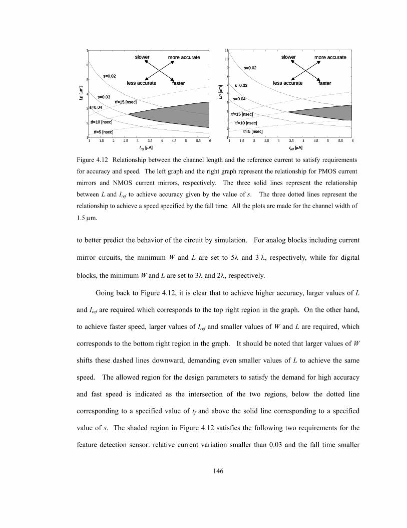
146
to better predict the behavior of the circuit by simulation. For analog blocks including current
mirror circuits, the minimum W and L are set to 5λ and 3 λ, respectively, while for digital
blocks, the minimum W and L are set to 3λ and 2λ, respectively.
Going back to Figure 4.12, it is clear that to achieve higher accuracy, larger values of L
and Iref are required which corresponds to the top right region in the graph. On the other hand,
to achieve faster speed, larger values of Iref and smaller values of W and L are required, which
corresponds to the bottom right region in the graph. It should be noted that larger values of W
shifts these dashed lines downward, demanding even smaller values of L to achieve the same
speed. The allowed region for the design parameters to satisfy the demand for high accuracy
and fast speed is indicated as the intersection of the two regions, below the dotted line
corresponding to a specified value of tf and above the solid line corresponding to a specified
value of s. The shaded region in Figure 4.12 satisfies the following two requirements for the
feature detection sensor: relative current variation smaller than 0.03 and the fall time smaller
more accurate
faster
slower
less accurates=0.02
s=0.03
s=0.04tf=15 [nsec]
tf=10 [nsec]
tf=5 [nsec]
s=0.02
s=0.03
s=0.04
tf=15 [nsec]
tf=10 [nsec]
tf=5 [nsec]
Iref [µA]
Ln[µ
m]
Lp[µ
m]
1 1.5 2 2.5 3 3.5 4 4.5 5 5.5 61
2
3
4
5
6
7
1 1.5 2 2.5 3 3.5 4 4.5 5 5.5 61
2
3
4
5
6
7
8
9
10
11
more accurate
faster
slower
less accurate
Iref [µA]
more accurate
faster
slower
less accurates=0.02
s=0.03
s=0.04tf=15 [nsec]
tf=10 [nsec]
tf=5 [nsec]
s=0.02
s=0.03
s=0.04
tf=15 [nsec]
tf=10 [nsec]
tf=5 [nsec]
Iref [µA]
Ln[µ
m]
Lp[µ
m]
1 1.5 2 2.5 3 3.5 4 4.5 5 5.5 61
2
3
4
5
6
7
1 1.5 2 2.5 3 3.5 4 4.5 5 5.5 61
2
3
4
5
6
7
8
9
10
11
more accurate
faster
slower
less accurate
Iref [µA] Figure 4.12 Relationship between the channel length and the reference current to satisfy requirements
for accuracy and speed. The left graph and the right graph represent the relationship for PMOS current
mirrors and NMOS current mirrors, respectively. The three solid lines represent the relationship
between L and Iref to achieve accuracy given by the value of s. The three dotted lines represent the
relationship to achieve a speed specified by the fall time. All the plots are made for the channel width of
1.5 µm.

147
than 10 nsec. The maximum allowed value for the fall time is set to 10 nsec, one tenth of one
operational cycle assuming a 10 MHz operation.
It should be mentioned that the shaded region for the NMOS case is shifted rightward
compared to that for the PMOS case, requiring more current to obtain the same speed and
accuracy. In other words, the PMOS current mirror operates faster than the NMOS current
mirror when the accuracy requirement is the same. The reason of this difference in the
performance is explained below. The ratio of the fall time for the PMOS transistor with respect
to that for the NMOS transistor is represented as
3
3
3
98
98
==
n
p
p
n
refn
nox
refp
pox
fn
fp
LL
IWLC
IWLC
tt
µµ
µ
µ (4.94)
where the same channel width is assumed for both NMOS and PMOS transistors. Since the
same accuracy is assumed for both NMOS and PMOS transistors,
refp
oxpV
refn
oxnV
IL
CA
IL
CAs TT
2
2
2
22 22 µµ
== . (4.95)
Therefore,
n
p
n
p
LL
µµ
=
. (4.96)
Eqn. (4.96) is substituted in (4.94) to generate
76.010435 4
141
413
=
=
=
=
=
oxn
oxp
n
p
n
p
p
n
fn
fp
CC
tt
µµ
µµ
µµ
µµ
(4.97)
where design parameters specified in eqns. (4.74) and (4.75) are used for calculation.
The above equation clearly indicates that the PMOS transistor operates about 24% faster
than the NMOS transistor. The design procedure imposing the same accuracy requirement for

148
both NMOS and PMOS transistors, in this sense, is not symmetric in terms of speed. The total
performance in terms of accuracy and speed is higher for the PMOS transistor than for the
NMOS transistors. However, other design procedures are possible. For example, an NMOS
transistor and a PMOS transistor can be designed to have the same speed by the adjustment of
W while keeping the same accuracy requirement; or the accuracy can be differently designed for
an NMOS transistor and a PMOS transistor while keeping the same speed. The choice of the
design procedure depends on the type of the application. In other words, the relative
importance of accuracy and speed determines the procedure. In the present design, more
emphasis was put on the accuracy requirement, resulting in the difference in the operational
speed for the NMOS transistor and the PMOS transistor.
From the shape of the shaded region in Figure 4.12, the use of a larger current is the only
way to satisfy both higher accuracy and faster operation. It is of course at the expense of
smaller power consumption. In the present design, the current level was chosen as 4 µA to
satisfy both speed and accuracy requirements without consuming too much power. For this
current, the channel length for the NMOS and PMOS transistors are chosen as 3.7 µm and
2.2 µm, respectively, to satisfy the accuracy requirement (see Table 4.3). The fall time is
estimated to be smaller than 10 nsec with this dimension for both the NMOS and PMOS
transistors. It is possible to further increase the current to realize more accuracy and higher
speed. However, in reality, the current must be restricted below some level to keep the
transistor in the saturation region, which is described next.
4.3.4 Consideration on the operating region
For a given W/L, a higher gate voltage is required to produce a large current. A high gate
voltage, however, may bring the transistor into the linear region when the drain voltage is
determined by other parts of the circuit. It is important to operate the transistor in the saturation
149
region so that a constant current is always supplied from the transistor. Let us analyze the
circuit shown in Figure 3.9. The following situation should be avoided: the bottom NMOS
transistors enter into the linear region by the lowering of the voltage of node Nc. This could
happen when node Nc is brought down by several current sources. For the feature detection
algorithm described before to work correctly, the current as large as three times Iref has to be
accommodated by the PMOS transistor without bringing down the voltage of node Nc too
much. The node voltage is given by
)/(
32
ppoxp
refTpDDC LWC
IVVV
µ×
−−= . (4.98)
This voltage is equal to the drain voltage of the current sinking NMOS transistor when
the resistance of NMOS switches is neglected. Therefore, Vc has to be higher than the gate
voltage of these transistors shifted downward by the threshold voltage VTn for NMOS transistors
to remain in the saturation region. This condition is expressed as
nn T
nnoxn
refTC V
LWCI
VV −+>)/(
2µ
. (4.99)
Substituting eqn. (4.98) into (4.99) yields
)/(
2)/(
32
nnoxn
ref
ppoxp
refTpDD LWC
ILWC
IVV
µµ>
×−− . (4.100)
Since the channel width is the same for both the NMOS and PMOS transistors, i.e., Wn =Wp
=W, the above equation reduces to
TpDDnoxn
ref
np
np VVLWC
ILL−<
+
)/(2
)/()/(3
1µµµ
. (4.101)
Substitution of eqn. (4.96) into eqn. (4.101) and further simplification yields

150
2
2
)(2
31 TpDDoxn
nref
p
n VVWC
LI−<
+
µµµ
. (4.102)
Finally the constraint on Ln as a function of the reference current Iref is obtained as:
( )
2
2
/312
+
−<
pnref
TpDDoxnn
I
VVCWL
µµ
µ. (4.103)
Lp can be obtained using eqns. (4.103) and (4.96).
The shaded region in Figure 4.12 satisfies eqn. (4.103), confirming the validity of the
previous selection of the reference current and the channel length. The restriction by the
operating region becomes more prominent if the narrower channel width is used. This is
exemplified in Figure 4.13 for W=0.9 [µm]. The maximum value of L decreases, as Iref becomes
larger. For both the PMOS and the NMOS cases, the fan-shaped shaded region originally
extended rightward reduces to a very small region. Any point inside this region satisfies the
three requirements so far requested: relative current variation smaller than 0.03; the fall time
smaller than 10 nsec, all transistors operate in the saturation region. If no overlapping region
exists, the value of W should be increased so that the requirement on the operating condition is
relaxed although the operational speed is slowed down.
It is interesting at this point to see the implication of the restriction by the operating
region. The following analysis is partly based on the work conducted by Kinget [4]. Let us
define the speed of the circuit as the reciprocal of the fall time, i.e.,
38
911WLC
Ikt
Speedox
ref
f
µ== (4.104)
where
ε
ε )1(2 −=k . (4.105)
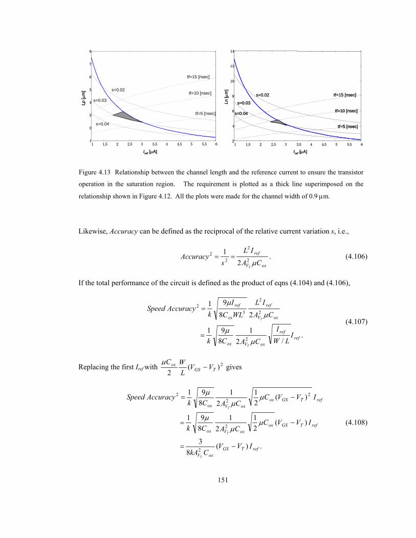
151
Likewise, Accuracy can be defined as the reciprocal of the relative current variation s, i.e.,
oxV
ref
CA
IL
sAccuracy
Tµ2
2
22
21
== . (4.106)
If the total performance of the circuit is defined as the product of eqns (4.104) and (4.106),
./2
1891
28
91
2
2
2
32
refref
oxVox
oxV
ref
ox
ref
ILW
I
CACk
CA
IL
WLC
Ik
AccuracySpeed
T
T
µµ
µ
µ
=
=
(4.107)
Replacing the first Iref with 2)(2 TGS
ox VVL
WC−
µ gives
.)(8
3
)(21
21
891
)(21
21
891
2
2
22
2
refTGSoxV
refTGSoxoxVox
refTGSoxoxVox
IVVCkA
IVVCCACk
IVVCCACk
AccuracySpeed
T
T
T
−=
−=
−=
µµ
µ
µµ
µ
(4.108)
tf=5 [nsec]
tf=10 [nsec]
tf=15 [nsec]
1 1.5 2 2.5 3 3.5 4 4.5 5 5.5 62
4
6
8
10
12
14
1 1.5 2 2.5 3 3.5 4 4.5 5 5.5 61
2
3
4
5
6
7
8
Lp[µ
m]
Ln[µ
m]
Iref [µA]Iref [µA]
s=0.02
s=0.03
s=0.04
s=0.02
s=0.03
s=0.04
tf=15 [nsec]
tf=10 [nsec]
tf=5 [nsec]
tf=5 [nsec]
tf=10 [nsec]
tf=15 [nsec]
1 1.5 2 2.5 3 3.5 4 4.5 5 5.5 62
4
6
8
10
12
14
1 1.5 2 2.5 3 3.5 4 4.5 5 5.5 61
2
3
4
5
6
7
8
Lp[µ
m]
Ln[µ
m]
Iref [µA]Iref [µA]
s=0.02
s=0.03
s=0.04
s=0.02
s=0.03
s=0.04
tf=15 [nsec]
tf=10 [nsec]
tf=5 [nsec]
Figure 4.13 Relationship between the channel length and the reference current to ensure the transistor
operation in the saturation region. The requirement is plotted as a thick line superimposed on the
relationship shown in Figure 4.12. All the plots were made for the channel width of 0.9 µm.
152
This equation states that the total performance in terms of speed and accuracy is
determined by the product of TGS VV − and Iref. The result is similar to what is described in ref.
[4]. Eqn. (4.108) can be rewritten as
)(
83
)(8
3
2
2
2
TGSDDoxV
DDref
refTGS
oxV
VVVCkA
VII
VVCkAPower
AccuracySpeed
T
T
−=
−=
(4.109)
where only DC power consumption is incorporated in the above formula. This is considered a
normalized total performance and is constant as long as the degree of biasing is the same. The
only way to increase the normalized total performance is to increase TGS VV − as much as
possible while ensuring the transistor operation in the saturation region. It is also clear from
eqn. (4.109) that higher performance is obtained for processes characterized by smaller
mismatch.
Along the curve shown as a thick line in Figure 4.13, TGS VV − is constant, indicating the
same normalized total performance. Moving to the right direction along this curve, the circuit
gains higher speed while losing accuracy and suffering from higher power consumption, but
still keeping the same normalized total performance. This is the maximum performance
obtained since this value of TGS VV − corresponds to the edge of the saturation region. If the
power consumption is not much of an issue, the best performance is obtained by choosing the
point where the TGS VV − constraint curve meets the accuracy requirement curve.
The difference of the performance between the PMOS and the NMOS transistors can be
explained from the point of biasing. The bias voltages for the PMOS and the NMOS transistors
for W = 1.5 µm are calculated as
=−NMOS.for ]V[51.0PMOSfor ]V[67.0
TGS VV (4.110)
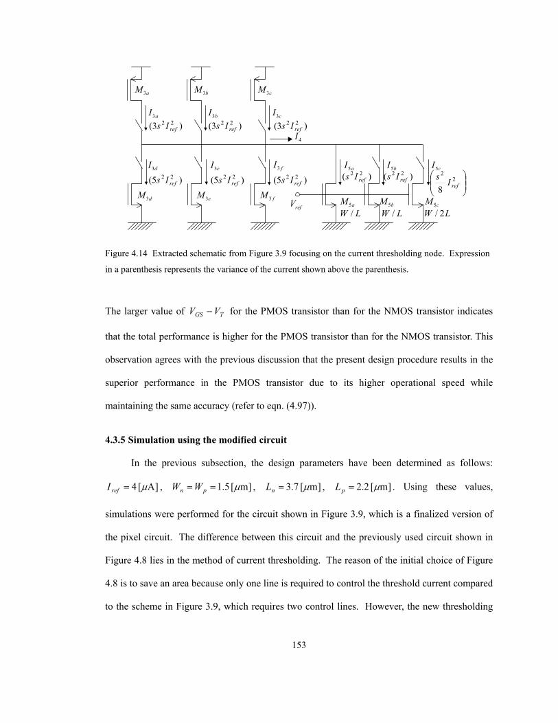
153
The larger value of TGS VV − for the PMOS transistor than for the NMOS transistor indicates
that the total performance is higher for the PMOS transistor than for the NMOS transistor. This
observation agrees with the previous discussion that the present design procedure results in the
superior performance in the PMOS transistor due to its higher operational speed while
maintaining the same accuracy (refer to eqn. (4.97)).
4.3.5 Simulation using the modified circuit
In the previous subsection, the design parameters have been determined as follows:
]A[4 µ=refI , ]m[5.1 µ== pn WW , ]m[7.3 µ=nL , ]m[2.2 µ=pL . Using these values,
simulations were performed for the circuit shown in Figure 3.9, which is a finalized version of
the pixel circuit. The difference between this circuit and the previously used circuit shown in
Figure 4.8 lies in the method of current thresholding. The reason of the initial choice of Figure
4.8 is to save an area because only one line is required to control the threshold current compared
to the scheme in Figure 3.9, which requires two control lines. However, the new thresholding
aM 3
aI3 bI3 cI3
bM 3 cM 3
dI3 eI3 fI3
dM 3 eM 3 fM 3
refV
4I
aM 5 bM 5 cM 5
LW /
aI5 bI5 cI5
)3( 22refIs )3( 22
refIs )3( 22refIs
)5( 22refIs )5( 22
refIs )5( 22refIs )( 22
refIs )( 22refIs
22
8 refIs
LW / LW 2/
Figure 4.14 Extracted schematic from Figure 3.9 focusing on the current thresholding node. Expression
in a parenthesis represents the variance of the current shown above the parenthesis.

154
scheme is simpler and does not have to distribute an analog signal in an entire chip area. In
addition, the new scheme is advantageous in terms of matching since a set of NMOS transistors
for current mirroring were removed and the new threshold current has less variation.
This is explained next using the simplified circuit shown in Figure 4.14. Due to lack of
an additional current mirror operation, the variance of the current I4 decreases to 14s2 and 19s2
when the current level is Iref and 2Iref, respectively, from the original variance of 18s2 and 21s2.
The variance of the threshold current is calculated as the summation of the variance of each of
the three currents (I5a, I5b, I5c) since there is no correlation between these currents. For I5=1.5Iref,
It is represented as
.89
),(89
),(21),(
)2,2/(),(
22
2
23
2
2225
ref
refI
refIrefI
refIrefII
Is
LI
LILI
LILI
=
=
+=
+=
σ
σσ
σσσ
(4.111)
Note that eqn. (4.33) is used to derive the current variation for the third current source
(transistor M5c), which employs half the channel length to produce half the reference current.
The probability density function given in eqns. (4.69), (4.70), and (4.71) are rewritten as
),14,2()( 222 refref IsINxp = (4.112)
)19,()( 221 refref IsINxp = , (4.113)
and
),)8/9(,5.1()( 225.1 refref IsINxp = (4.114)
respectively. Note that the variance is smaller than those obtained in the previous design (eqns.
(4.69), (4.70), and (4.71)). The expected error rate for these distributions is plotted as a function
of s in Figure 4.15 with the Hspice Monte-Carlo simulation result. In the Hspice simulation,
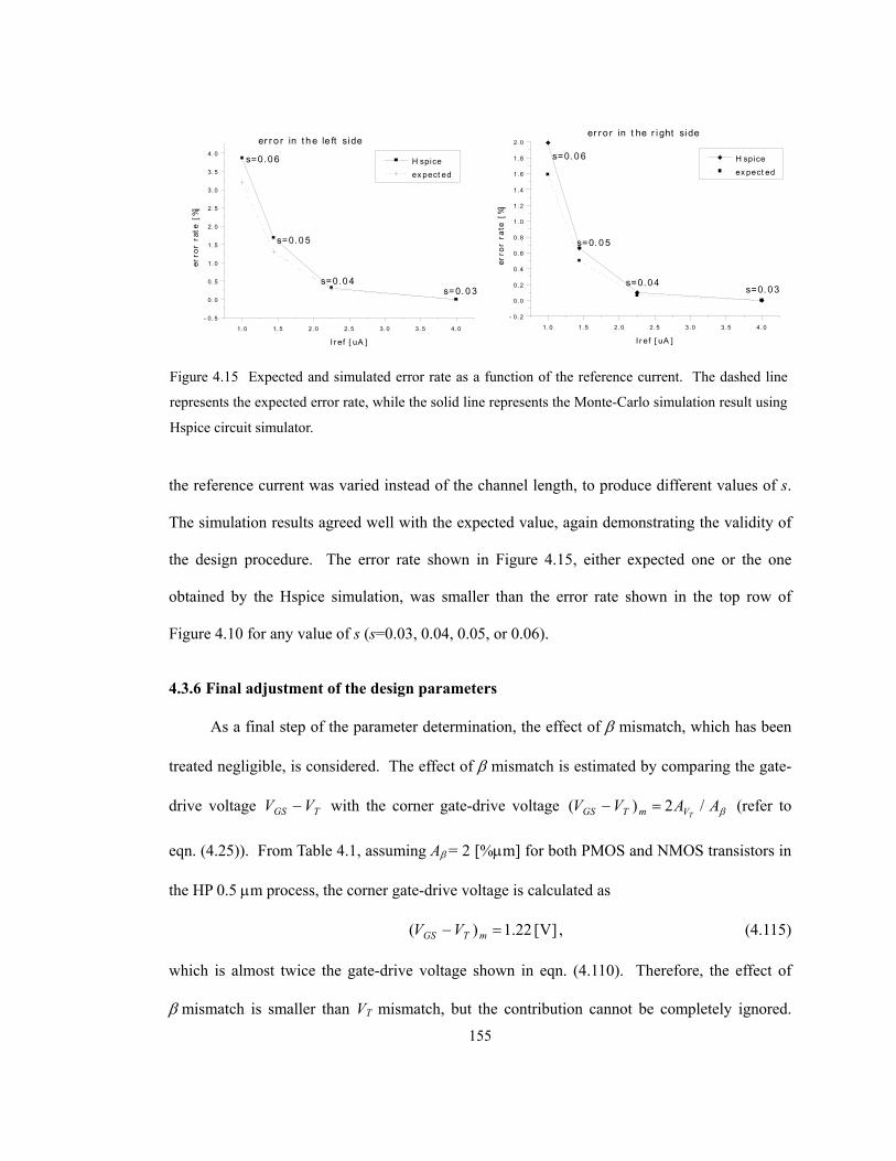
155
the reference current was varied instead of the channel length, to produce different values of s.
The simulation results agreed well with the expected value, again demonstrating the validity of
the design procedure. The error rate shown in Figure 4.15, either expected one or the one
obtained by the Hspice simulation, was smaller than the error rate shown in the top row of
Figure 4.10 for any value of s (s=0.03, 0.04, 0.05, or 0.06).
4.3.6 Final adjustment of the design parameters
As a final step of the parameter determination, the effect of β mismatch, which has been
treated negligible, is considered. The effect of β mismatch is estimated by comparing the gate-
drive voltage TGS VV − with the corner gate-drive voltage βAAVVTVmTGS /2)( =− (refer to
eqn. (4.25)). From Table 4.1, assuming Aβ = 2 [%µm] for both PMOS and NMOS transistors in
the HP 0.5 µm process, the corner gate-drive voltage is calculated as
]V[22.1)( =− mTGS VV , (4.115)
which is almost twice the gate-drive voltage shown in eqn. (4.110). Therefore, the effect of
β mismatch is smaller than VT mismatch, but the contribution cannot be completely ignored.
1. 0 1. 5 2. 0 2. 5 3. 0 3. 5 4. 0- 0. 5
0. 0
0. 5
1. 0
1. 5
2. 0
2. 5
3. 0
3. 5
4. 0 s=0. 06
s=0.0 5
s=0. 0 3s=0. 0 4
er r o r in t h e le ft side
H spice ex pect ed
erro
r ra
te [
%]
I r ef [ uA ]
1. 0 1. 5 2. 0 2. 5 3. 0 3. 5 4. 0- 0. 2
0. 0
0. 2
0. 4
0. 6
0. 8
1. 0
1. 2
1. 4
1. 6
1. 8
2. 0
s=0. 0 6
s=0. 0 5
s=0.0 4s=0. 03
H spice ex pect ed
er r o r in t he r i ght side
erro
r ra
te [
%]
I r ef [ uA ]
Figure 4.15 Expected and simulated error rate as a function of the reference current. The dashed line
represents the expected error rate, while the solid line represents the Monte-Carlo simulation result using
Hspice circuit simulator.
156
The error rate increases from 0.03 to 0.037 and to 0.034 for the PMOS and the NMOS
transistors, respectively by incorporating the effect of β mismatch. The PMOS transistor is
more affected than the NMOS transistor due to its smaller area. This increase should be
compensated by the increase in L so that the overall relative current variation remains 0.03. As
a final value, L is chosen as 2.7 µm and 4.2 µm for the PMOS and the NMOS transistors,
respectively.
4.3.7 Summary of the design procedure
A systematic design procedure that determines the transistor dimension and the reference
current to satisfy the given specification in terms of accuracy and speed has been presented in
this section. The procedure is briefly summarized below. First, a given accuracy requirement
has to be converted to the requirement for the current variation. It is possible by representing
the variable concerning accuracy, such as an error rate, as a function of the current variation.
The formulas derived in the previous section are necessary for this representation. Next, the
minimum value of L2Iref is determined to satisfy the required current variation. In other words,
the allowed region for L and Iref can be graphically obtained as the region above a constraint
curve.
Another requirement concerning speed gives the maximum value of refIWL /3 . W is
chosen as the minimum dimension as an initial choice. For this value of W, the allowed region
for L and Iref can be graphically represented as the region below another constraint curve. At
this point, the allowed combinations of L and Iref can be represented as an intersection of the
above two regions, which takes a fan shape extended rightward. Next, the operating region of
the transistor has to be examined. The constraint for transistors to stay in the saturation region,
which is given as the maximum value of TGS VV − or )//( LWI ref , can be also graphically

157
represented on the same graph. By this constraint, the allowed region may reduce to a
triangular shape. If no region exists to satisfy this constraint on the operating region, W has to
be increased to relax the condition and the above procedure has to be repeated.
The final selection from the triangular region depends on the type of applications. It
should be decided by considering the relative importance of accuracy and speed as well as the
power consumption. One of the selection methods when the power consumption is not too
high within the allowed region is to choose the values of L and Iref which correspond to the
bottom right vertex of the triangle, since the total performance (not normalized) in terms of
speed and power is maximum at this point.
4.4 Summary
A systematic design procedure based on transistor mismatch analysis for current-mode
processing circuits has been proposed in this section. First, the formula relating the design
parameters to the current variation and the other formula describing the increase in the current
variation by current mirroring are newly derived. The effect of correlation between multiple
currents is also formulated. Using these formulas, the proposed method converts the
requirement for accuracy and speed to the requirement for the design parameters (W, L, Iref).
The condition for ensuring the transistor operation in the saturation region is also converted to
the other form of requirement. The design parameters are chosen to satisfy all the above three
requirements. It was found that the normalized total performance is kept constant as long as the
degree of transistor biasing is the same. The transistor dimension for the current mirror circuit
employed for the feature detection sensor has been determined using the proposed method to
achieve an error rate smaller than 0.0001 and the fall time smaller than 10 nsec.

158
4.5 References
[1] K. Lakshmikumar, R. Hadaway, and M. Copeland, “Characterization and modeling of
mismatch in MOS transistors for precision analog design,” IEEE J. Solid-State Circuits, vol. 21,
no. 6, pp. 1057-1066, 1986.
[2] M. Pelgrom, “Matching properties of MOS transistors,” IEEE J. Solid-State Circuits, vol.
24, no. 5, pp. 1433-1440, 1989.
[3] J. Bastos, M. Steyaert, R. Roovers, P. Kinget, W. Sansen, B. Graindourze, A. Pergoot, and
Er. Janssens, “Mismatch characterization of small size MOS transistors,” Proc. IEEE Int.
Conference on Microelectronic Test Structures, (Nara, Japan), pp. 271-276, March, 1995.
[4] P. Kinget and M. Steyaert, Analog VLSI Integration of Massively Parallel Processing
Systems, Kluwer Academic Publishers, 1996.
[5] S. J. Lovett, M. W. Welten, A. Mathewson, B. Mason, “Optimizing MOS transistor
mismatch,” IEEE J. Solid-State Circuits, vol. 33, no. 1, pp. 147-150, 1998.
159
Chapter 5 Implementation and experiments
Design parameters for current mirror circuits have been determined in the previous
chapter using the newly proposed systematic design procedure. With these parameters, transient
simulations are performed in this chapter. Based on this result, additional mechanisms for
achieving faster operation are presented. Other implementation related issues including control
circuits are also discussed. Then experimental results using the prototype sensor are presented
in detail to demonstrate its functionality. The performance of the sensor is characterized by
several important parameters concerning the mismatch and the operational speed.
5.1 Transient behavior of the circuit
In the previous chapter, the reference current and the dimension of transistors used for
current sources have been determined using a systematic design procedure to satisfy given
requirements for accuracy and speed. The speed estimate, however, is valid only for a simple
current mirror consisting of two transistors. Hence, the overall operational speed has to be
examined for the entire circuit, which contains several variations of current mirror circuit.
From a closer look of the circuit shown in Figure 3.9, it is obvious that the operational
speed is mainly limited by the time required for charging and discharging node Nc. This is the
most critical node determining the overall operational speed due to its large capacitance since
thirteen PMOS gates are connected to this node. The charging and discharging behavior can be
analyzed by considering this circuit as a flipped version of Figure 4.11 with additional eleven
transistors (thirteen transistors in total). The load capacitance C is estimated as 120 fF for
thirteen PMOS transistors. Hence, the rise time and the fall time are calculated using eqns.
(4.86) and (4.92) as

160
)95.0()nsec(3.48 == αrt , (5.1)
and
)05.0(sec)n(9.76 == εft , (5.2)
respectively.
To confirm these estimated values and to investigate the dynamic behavior of the circuit,
transient simulation was performed using the Hspice simulator. The line completion operation,
which has been described in Section 2.6.4, was used in the simulation. The formulas (eqn.
(2.42) to (2.48)) for the line completion are rewritten below to explicitly specify memories used
for operation:
op1 (line elongation in o0 ): )M()M(M x,xa 13
13 aa IALEa TT == , (5.3)
op2 (linestop detection): )M()M(M a,a8y 88 LSDLSD IALSD TT == , (5.4)
op3: (removal of the linestops) )MM(M ya5.0,y −= ET (5.5)
with
=
−−−−−−−−
=
=
111111111
,111121111
,000111000
813 EAA LSDa , (5.6)
5.0813 == LSDa II . (5.7)
Figure 5.1 shows the expected evolution pattern when the line completion operation is
applied for a single isolated point. Figure 5.2 shows the simulation results obtained at the clock
op1 op2 op3
Figure 5.1 Expected evolution pattern when the line completion operation is applied for a single isolated
point. See text for the specification for op1, op2, and op3 operations.
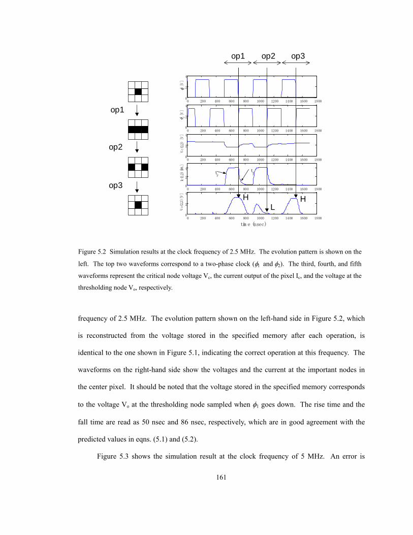
161
frequency of 2.5 MHz. The evolution pattern shown on the left-hand side in Figure 5.2, which
is reconstructed from the voltage stored in the specified memory after each operation, is
identical to the one shown in Figure 5.1, indicating the correct operation at this frequency. The
waveforms on the right-hand side show the voltages and the current at the important nodes in
the center pixel. It should be noted that the voltage stored in the specified memory corresponds
to the voltage Vo at the thresholding node sampled when φ1 goes down. The rise time and the
fall time are read as 50 nsec and 86 nsec, respectively, which are in good agreement with the
predicted values in eqns. (5.1) and (5.2).
Figure 5.3 shows the simulation result at the clock frequency of 5 MHz. An error is
0 200 400 600 800 1000 1200 1400 1600 18000
2
4
φ 1 [V]
0 200 400 600 800 1000 1200 1400 1600 18000
2
4
φ 2 [V]
0 200 400 600 800 1000 1200 1400 1600 18000
2
4
Vc(2,2) [V
]
0 200 400 600 800 1000 1200 1400 1600 18000
2
4
Ic(2,2) [µ A
]
0 200 400 600 800 1000 1200 1400 1600 18000
2
4
tim e (nsec)
Vo(2,2) [V
]
tr t
f
op1
op2
op3
op1 op2 op3
HL
H
Figure 5.2 Simulation results at the clock frequency of 2.5 MHz. The evolution pattern is shown on the
left. The top two waveforms correspond to a two-phase clock (φ1 and φ2). The third, fourth, and fifth
waveforms represent the critical node voltage Vc, the current output of the pixel Ic, and the voltage at the
thresholding node Vo, respectively.
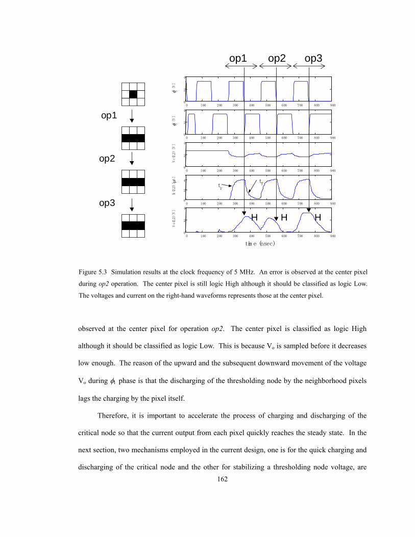
162
observed at the center pixel for operation op2. The center pixel is classified as logic High
although it should be classified as logic Low. This is because Vo is sampled before it decreases
low enough. The reason of the upward and the subsequent downward movement of the voltage
Vo during φ1 phase is that the discharging of the thresholding node by the neighborhood pixels
lags the charging by the pixel itself.
Therefore, it is important to accelerate the process of charging and discharging of the
critical node so that the current output from each pixel quickly reaches the steady state. In the
next section, two mechanisms employed in the current design, one is for the quick charging and
discharging of the critical node and the other for stabilizing a thresholding node voltage, are
0 100 200 300 400 500 600 700 800 9000
2
4
φ 1 [V]
0 100 200 300 400 500 600 700 800 9000
2
4
φ 2 [V]
0 100 200 300 400 500 600 700 800 9000
2
4
Vc(2,2) [V]
0 100 200 300 400 500 600 700 800 9000
2
4
Ic(2,2) [ µ
A]
0 100 200 300 400 500 600 700 800 9000
2
4
tim e (nsec)
Vo(2,2) [V
]
tr tf
op1 op2 op3
HHH
op1
op2
op3
Figure 5.3 Simulation results at the clock frequency of 5 MHz. An error is observed at the center pixel
during op2 operation. The center pixel is still logic High although it should be classified as logic Low.
The voltages and current on the right-hand waveforms represents those at the center pixel.
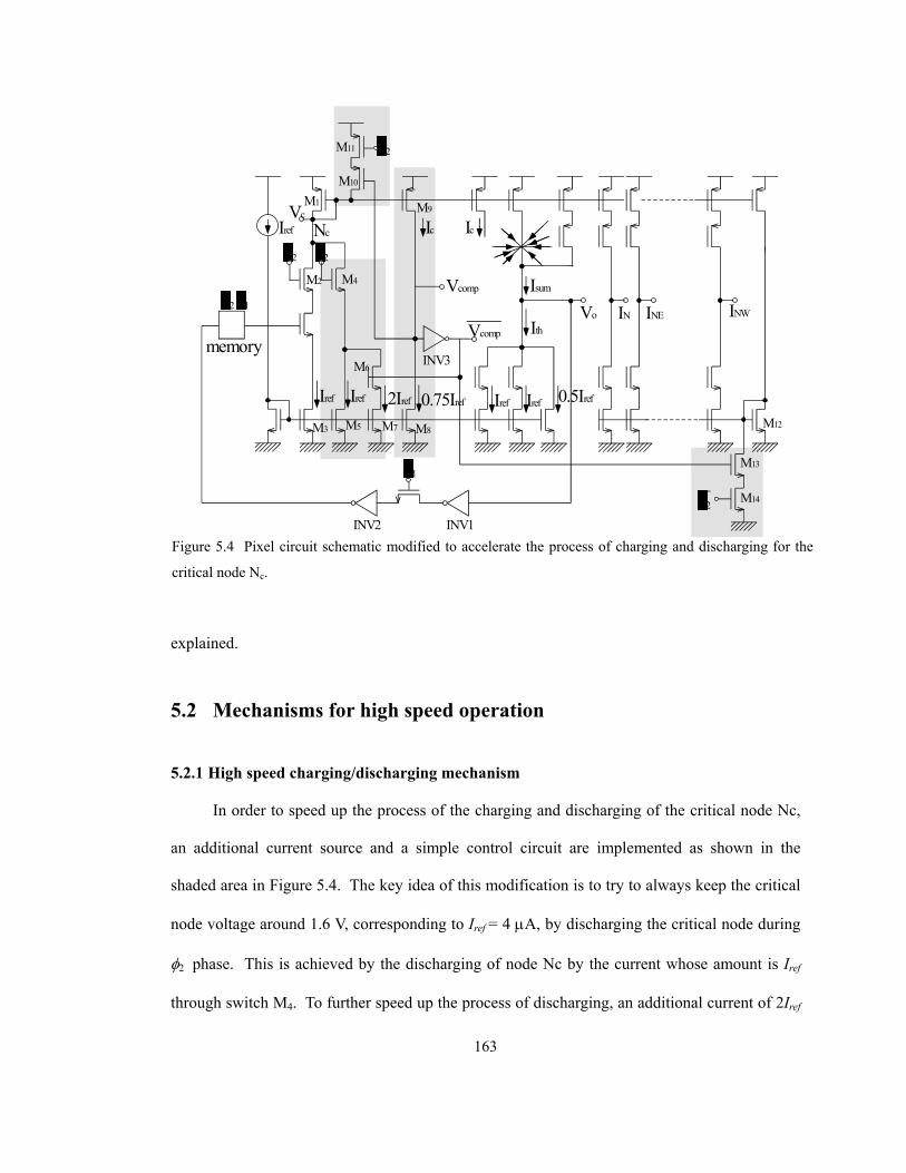
163
explained.
5.2 Mechanisms for high speed operation
5.2.1 High speed charging/discharging mechanism
In order to speed up the process of the charging and discharging of the critical node Nc,
an additional current source and a simple control circuit are implemented as shown in the
shaded area in Figure 5.4. The key idea of this modification is to try to always keep the critical
node voltage around 1.6 V, corresponding to Iref = 4 µA, by discharging the critical node during
φ2 phase. This is achieved by the discharging of node Nc by the current whose amount is Iref
through switch M4. To further speed up the process of discharging, an additional current of 2Iref
IthIN INE INW
Iref
0.5IrefIrefIrefIref
Vo
1
2
2
2
2 1
memory
0.75Iref2Iref
Isum
IcNc
Iref
M1
M2
M3
M4
M5
M6
INV1
M7
M10
M9
M8
M11
M13
M14
Vc
2
Vcomp
M12
Vcomp
Ic
INV2
INV3
Figure 5.4 Pixel circuit schematic modified to accelerate the process of charging and discharging for the
critical node Nc.
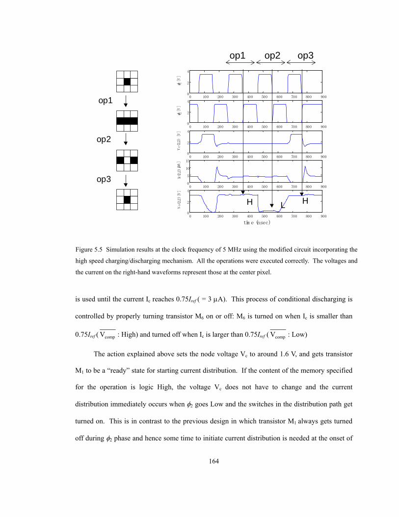
164
is used until the current Ic reaches 0.75Iref ( = 3 µA). This process of conditional discharging is
controlled by properly turning transistor M6 on or off: M6 is turned on when Ic is smaller than
0.75Iref ( compV : High) and turned off when Ic is larger than 0.75Iref ( compV : Low)
The action explained above sets the node voltage Vc to around 1.6 V, and gets transistor
M1 to be a “ready” state for starting current distribution. If the content of the memory specified
for the operation is logic High, the voltage Vc does not have to change and the current
distribution immediately occurs when φ2 goes Low and the switches in the distribution path get
turned on. This is in contrast to the previous design in which transistor M1 always gets turned
off during φ2 phase and hence some time to initiate current distribution is needed at the onset of
0 100 200 300 400 500 600 700 800 9000
2
4
φ 1 [V]
0 100 200 300 400 500 600 700 800 9000
2
4
φ 2 [V]
0 100 200 300 400 500 600 700 800 9000
2
4
Vc(2,2) [V]
0 100 200 300 400 500 600 700 800 9000
5
10
15
Ic(2,2) [µ A
]
0 100 200 300 400 500 600 700 800 9000
2
4
tim e (nsec)
Vo(2,2) [V]
op1 op2 op3
LH H
op1
op2
op3
Figure 5.5 Simulation results at the clock frequency of 5 MHz using the modified circuit incorporating the
high speed charging/discharging mechanism. All the operations were executed correctly. The voltages and
the current on the right-hand waveforms represent those at the center pixel.
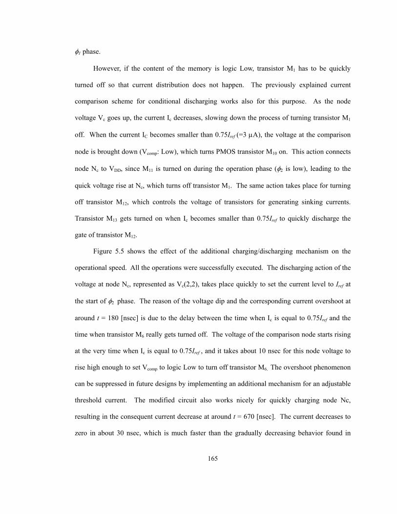
165
φ1 phase.
However, if the content of the memory is logic Low, transistor M1 has to be quickly
turned off so that current distribution does not happen. The previously explained current
comparison scheme for conditional discharging works also for this purpose. As the node
voltage Vc goes up, the current Ic decreases, slowing down the process of turning transistor M1
off. When the current IC becomes smaller than 0.75Iref (=3 µA), the voltage at the comparison
node is brought down (Vcomp: Low), which turns PMOS transistor M10 on. This action connects
node Nc to VDD, since M11 is turned on during the operation phase (φ2 is low), leading to the
quick voltage rise at Nc, which turns off transistor M1. The same action takes place for turning
off transistor M12, which controls the voltage of transistors for generating sinking currents.
Transistor M13 gets turned on when Ic becomes smaller than 0.75Iref to quickly discharge the
gate of transistor M12.
Figure 5.5 shows the effect of the additional charging/discharging mechanism on the
operational speed. All the operations were successfully executed. The discharging action of the
voltage at node Nc, represented as Vc(2,2), takes place quickly to set the current level to Iref at
the start of φ2 phase. The reason of the voltage dip and the corresponding current overshoot at
around t = 180 [nsec] is due to the delay between the time when Ic is equal to 0.75Iref and the
time when transistor M6 really gets turned off. The voltage of the comparison node starts rising
at the very time when Ic is equal to 0.75Iref , and it takes about 10 nsec for this node voltage to
rise high enough to set Vcomp to logic Low to turn off transistor M6. The overshoot phenomenon
can be suppressed in future designs by implementing an additional mechanism for an adjustable
threshold current. The modified circuit also works nicely for quickly charging node Nc,
resulting in the consequent current decrease at around t = 670 [nsec]. The current decreases to
zero in about 30 nsec, which is much faster than the gradually decreasing behavior found in
166
Figure 5.3.
The high speed charging/discharging mechanism fails at the frequency of 10 MHz as
shown in Figure 5.6. The failure occurs at the pixel (1,2) and pixel (3,2) instead of the center
pixel (2,2): the pixel output is high after op1 operation. The voltage profile at the thresholding
node Vo(1,2) explains the mechanism of the error. The voltage Vo is initially set to logic High at
the onset of φ1 phase. Note that at this point all the pixels including pixels (1,1), (1,2), and (1,3)
are set to a “ready” state for current distribution by the previously described high speed
charging mechanism. All these pixels contribute to the positive current flow to the thresholding
node at pixel (1,2) since the template for op1 operation works for horizontal enhancement.
Then, the current Ic at these pixels decreases to zero by the high speed discharging mechanism
0 50 100 150 200 250 300 350 400 450 5000
2
4
φ 1 [V]
0 50 100 150 200 250 300 350 400 450 5000
2
4
φ 2 [V]
0 50 100 150 200 250 300 350 400 450 5000
2
4
Vc(1,2) [V
]0 50 100 150 200 250 300 350 400 450 500
0
5
10
15
Ic(1,2) [µ A
]
0 50 100 150 200 250 300 350 400 450 5000
2
4
Vo(1,2) [V]
tim e (nsec)
op1 op2 op3
LH
L
pixel (1,2)
op1
op2
op3
Figure 5.6 Simulation results at the clock frequency of 10 MHz using the modified circuit incorporating
the high speed charging/discharging mechanism. An error was observed for op1 operation at the pixel
(1,2). The voltages and the current on the right-hand waveforms represent those at the pixel (1,2).
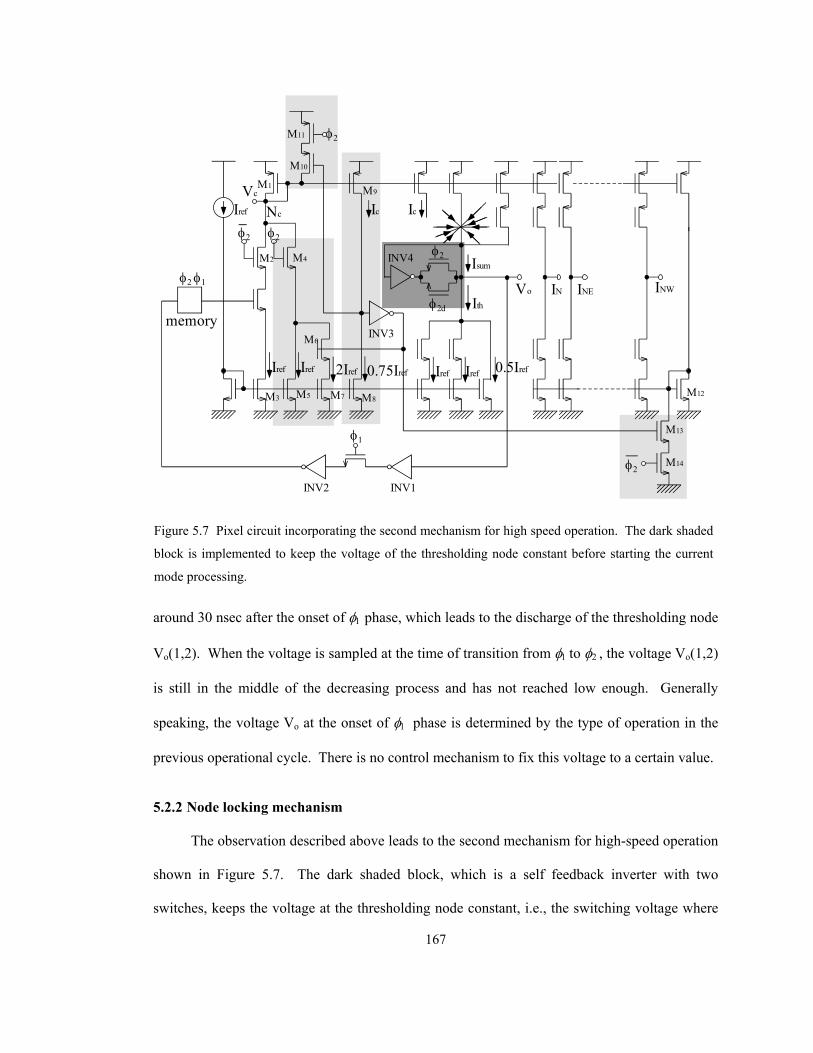
167
around 30 nsec after the onset of φ1 phase, which leads to the discharge of the thresholding node
Vo(1,2). When the voltage is sampled at the time of transition from φ1 to φ2 , the voltage Vo(1,2)
is still in the middle of the decreasing process and has not reached low enough. Generally
speaking, the voltage Vo at the onset of φ1 phase is determined by the type of operation in the
previous operational cycle. There is no control mechanism to fix this voltage to a certain value.
5.2.2 Node locking mechanism
The observation described above leads to the second mechanism for high-speed operation
shown in Figure 5.7. The dark shaded block, which is a self feedback inverter with two
switches, keeps the voltage at the thresholding node constant, i.e., the switching voltage where
φ2INV4
IthIN INE INW
Iref
0.5IrefIrefIrefIref
Vo
φ1
φ2
φ2
φ2
φ2 φ1
memory
0.75Iref2Iref
Isum
IcNc
Iref
M1
M2
M3
M4
M5
M6
INV1
M7
M10
M9
M8
M11
M13
M14
Vc
φ2
M12
Ic
INV2
INV3
φ2d
Figure 5.7 Pixel circuit incorporating the second mechanism for high speed operation. The dark shaded
block is implemented to keep the voltage of the thresholding node constant before starting the current
mode processing.
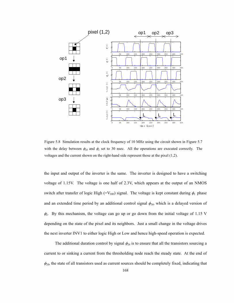
168
the input and output of the inverter is the same. The inverter is designed to have a switching
voltage of 1.15V. The voltage is one half of 2.3V, which appears at the output of an NMOS
switch after transfer of logic High (=VDD) signal. The voltage is kept constant during φ2 phase
and an extended time period by an additional control signal φ2d, which is a delayed version of
φ2. By this mechanism, the voltage can go up or go down from the initial voltage of 1.15 V
depending on the state of the pixel and its neighbors. Just a small change in the voltage drives
the next inverter INV1 to either logic High or Low and hence high-speed operation is expected.
The additional duration control by signal φ2d is to ensure that all the transistors sourcing a
current to or sinking a current from the thresholding node reach the steady state. At the end of
φ2d, the state of all transistors used as current sources should be completely fixed, indicating that
0 50 100 150 200 250 300 350 400 4500
2
4
φ 1 [V]
0 50 100 150 200 250 300 350 400 4500
2
4
φ 2 [V]
0 50 100 150 200 250 300 350 400 4500
2
4
φ 2d [V]
0 50 100 150 200 250 300 350 400 4500
2
4
Vc(1,2) [V]
0 50 100 150 200 250 300 350 400 4500
5
10
15
Ic(1,2) [µ A
]
0 50 100 150 200 250 300 350 400 4500
2
4
Vo(1,2) [V]
tim e (nsec)
op1 op2 op3
LL L
pixel (1,2)
op1
op2
op3
Figure 5.8 Simulation results at the clock frequency of 10 MHz using the circuit shown in Figure 5.7
with the delay between φ2d and φ2 set to 30 nsec. All the operations are executed correctly. The
voltages and the current shown on the right-hand side represent those at the pixel (1,2).
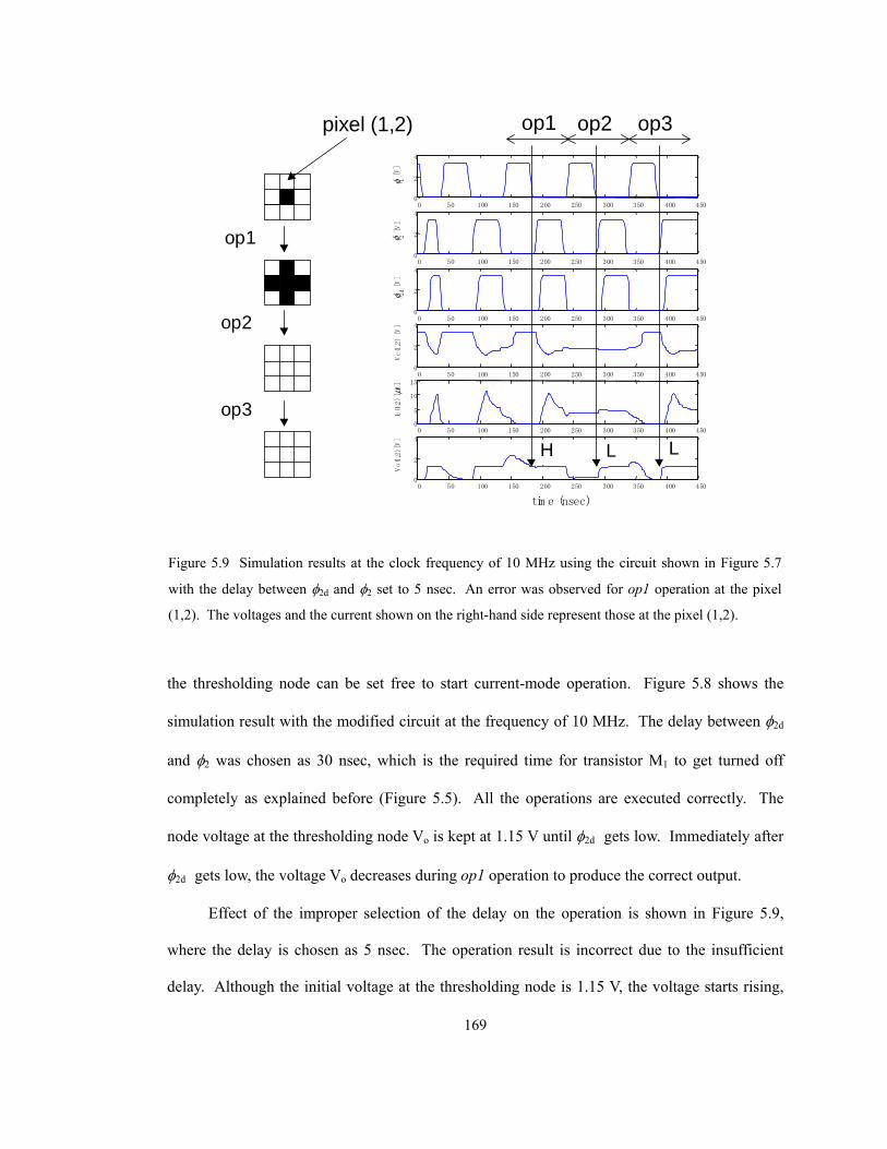
169
the thresholding node can be set free to start current-mode operation. Figure 5.8 shows the
simulation result with the modified circuit at the frequency of 10 MHz. The delay between φ2d
and φ2 was chosen as 30 nsec, which is the required time for transistor M1 to get turned off
completely as explained before (Figure 5.5). All the operations are executed correctly. The
node voltage at the thresholding node Vo is kept at 1.15 V until φ2d gets low. Immediately after
φ2d gets low, the voltage Vo decreases during op1 operation to produce the correct output.
Effect of the improper selection of the delay on the operation is shown in Figure 5.9,
where the delay is chosen as 5 nsec. The operation result is incorrect due to the insufficient
delay. Although the initial voltage at the thresholding node is 1.15 V, the voltage starts rising,
0 50 100 150 200 250 300 350 400 4500
2
4
φ 1 [V]
0 50 100 150 200 250 300 350 400 4500
2
4
φ 2 [V]
0 50 100 150 200 250 300 350 400 4500
2
4
φ 2d [V]
0 50 100 150 200 250 300 350 400 4500
2
4
Vc(1,2) [V]
0 50 100 150 200 250 300 350 400 4500
5
10
15
Ic(1,2) [µA]
0 50 100 150 200 250 300 350 400 4500
2
4
Vo(1,2) [V]
tim e (nsec)
op1 op2 op3
LH L
pixel (1,2)
op1
op2
op3
Figure 5.9 Simulation results at the clock frequency of 10 MHz using the circuit shown in Figure 5.7
with the delay between φ2d and φ2 set to 5 nsec. An error was observed for op1 operation at the pixel
(1,2). The voltages and the current shown on the right-hand side represent those at the pixel (1,2).
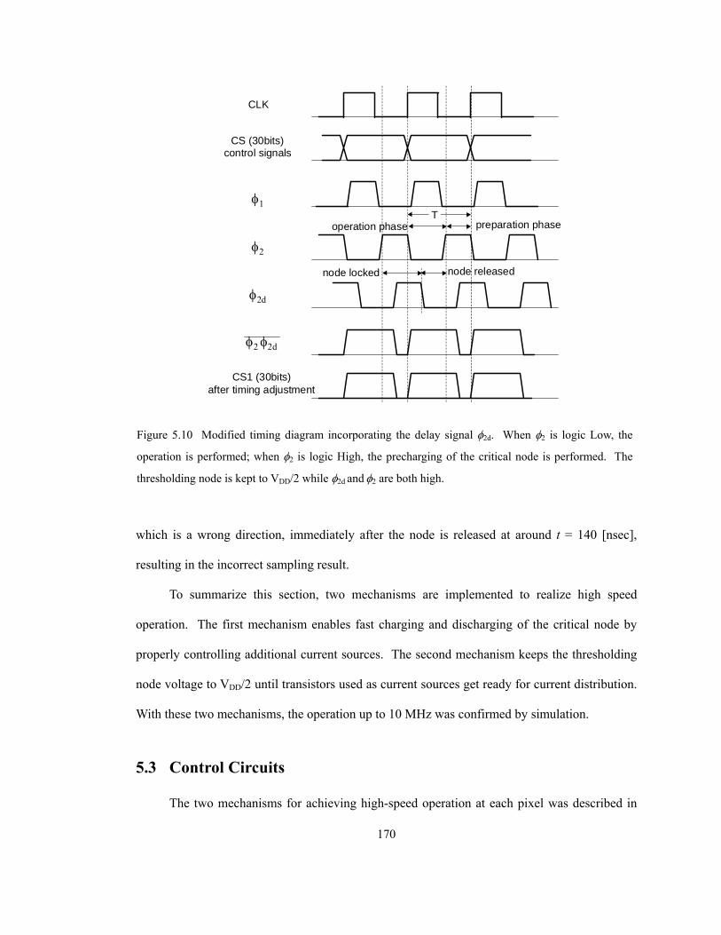
170
which is a wrong direction, immediately after the node is released at around t = 140 [nsec],
resulting in the incorrect sampling result.
To summarize this section, two mechanisms are implemented to realize high speed
operation. The first mechanism enables fast charging and discharging of the critical node by
properly controlling additional current sources. The second mechanism keeps the thresholding
node voltage to VDD/2 until transistors used as current sources get ready for current distribution.
With these two mechanisms, the operation up to 10 MHz was confirmed by simulation.
5.3 Control Circuits
The two mechanisms for achieving high-speed operation at each pixel was described in
φ1
φ2
φ2d
CS (30bits)control signals
φ2 φ2d
node locked
CLK
Toperation phase preparation phase
node released
CS1 (30bits)after timing adjustment
Figure 5.10 Modified timing diagram incorporating the delay signal φ2d. When φ2 is logic Low, the
operation is performed; when φ2 is logic High, the precharging of the critical node is performed. The
thresholding node is kept to VDD/2 while φ2d and φ2 are both high.
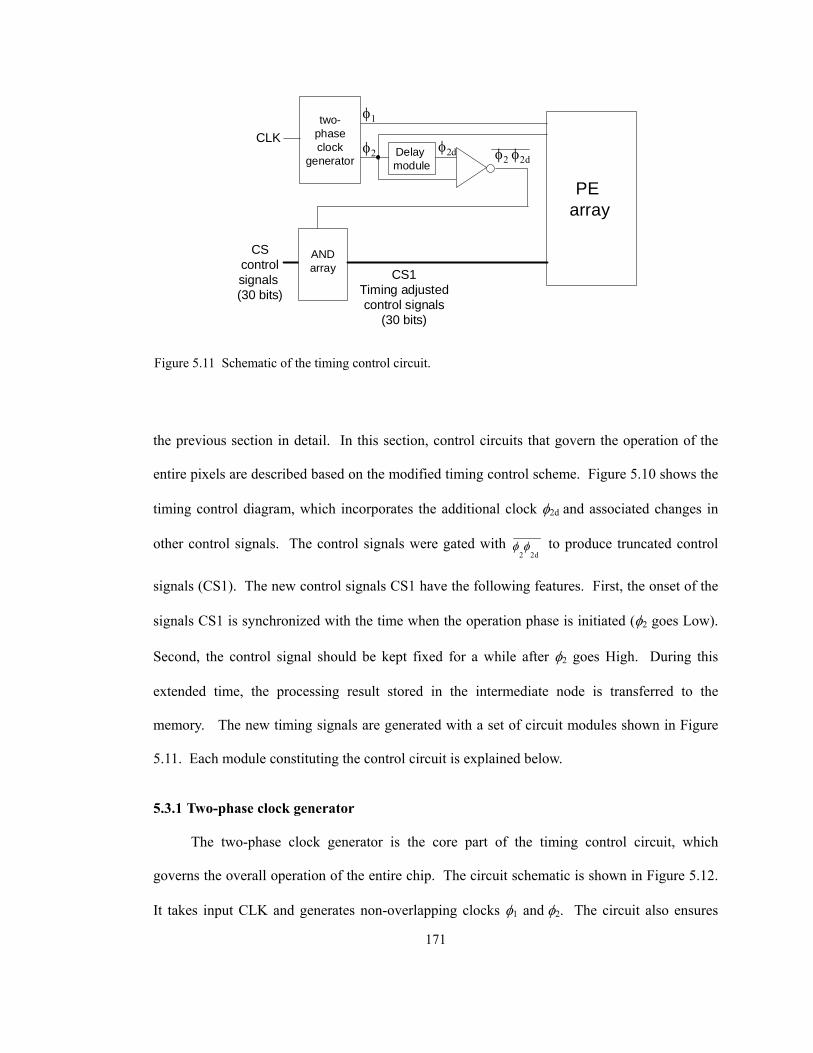
171
the previous section in detail. In this section, control circuits that govern the operation of the
entire pixels are described based on the modified timing control scheme. Figure 5.10 shows the
timing control diagram, which incorporates the additional clock φ2d and associated changes in
other control signals. The control signals were gated with d22
φφ to produce truncated control
signals (CS1). The new control signals CS1 have the following features. First, the onset of the
signals CS1 is synchronized with the time when the operation phase is initiated (φ2 goes Low).
Second, the control signal should be kept fixed for a while after φ2 goes High. During this
extended time, the processing result stored in the intermediate node is transferred to the
memory. The new timing signals are generated with a set of circuit modules shown in Figure
5.11. Each module constituting the control circuit is explained below.
5.3.1 Two-phase clock generator
The two-phase clock generator is the core part of the timing control circuit, which
governs the overall operation of the entire chip. The circuit schematic is shown in Figure 5.12.
It takes input CLK and generates non-overlapping clocks φ1 and φ2. The circuit also ensures
CLKtwo-
phaseclock
generator
φ1
φ2 Delay module
φ2d
CScontrolsignals (30 bits)
φ2 φ2d
CS1Timing adjustedcontrol signals
(30 bits)
ANDarray
PE array
Figure 5.11 Schematic of the timing control circuit.

172
that both φ1 and φ2 do not become logic High at the same time by self-feedback mechanism.
For example, if φ1 is logic High, the NOR gate (NOR1) forces the output φ2 to logic Low, and
vice versa. A set of strong inverters (INV3 and INV5) are used at the output stage to drive a
large number of signal lines running all through the entire chip and gate capacitance connected
to them. The inverter is designed to drive a load capacitance of 10 pF, which is an estimated
value for the accumulated load.
5.3.2 Programmable delay module
From the simulation results in the previous section, the delay of φ2d with respect to φ2
should be around 30 nsec, which corresponds to the time for the current sourcing PMOS
transistors to get turned off. This estimate, however, may be altered by some unexpected
reasons in real experiments. Therefore, a delay module is designed to produce various delays
according to the external settings. The circuit is shown in Figure 5.13. It consists of a series of
seven delay units, eight transmission gates, and a multiplexer. The delay unit consists of two
C LK
φ 1
φ 2
(150/0.9)
(60/0.9)
(4.8/0.9)
(1.5/0.9)
(1.5/0.9)
NOR1
NOR2
INV1
INV2 INV3
INV4 INV5
Figure 5.12 Schematic of the two-phase clock generator.
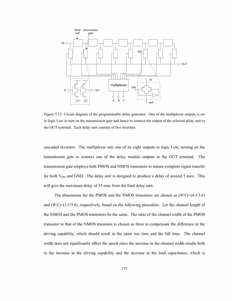
173
cascaded inverters. The multiplexer sets one of its eight outputs to logic Low, turning on the
transmission gate to connect one of the delay module outputs to the OUT terminal. The
transmission gate employs both PMOS and NMOS transistors to ensure complete signal transfer
for both VDD and GND. The delay unit is designed to produce a delay of around 5 nsec. This
will give the maximum delay of 35 nsec from the final delay unit.
The dimensions for the PMOS and the NMOS transistors are chosen as (W/L)=(4.5/3.6)
and (W/L)=(1.5/3.6), respectively, based on the following procedure. Let the channel length of
the NMOS and the PMOS transistors be the same. The ratio of the channel width of the PMOS
transistor to that of the NMOS transistor is chosen as three to compensate the difference in the
driving capability, which should result in the same rise time and the fall time. The channel
width does not significantly affect the speed since the increase in the channel width results both
in the increase in the driving capability and the increase in the load capacitance, which is
A B C
multiplexerin out
IN
OUT
SW
SW
delayunit
in
out
transmissiongate
Figure 5.13 Circuit diagram of the programmable delay generator. One of the multiplexer outputs is set
to logic Low to turn on the transmission gate and hence to connect the output of the selected delay unit to
the OUT terminal. Each delay unit consists of two inverters.
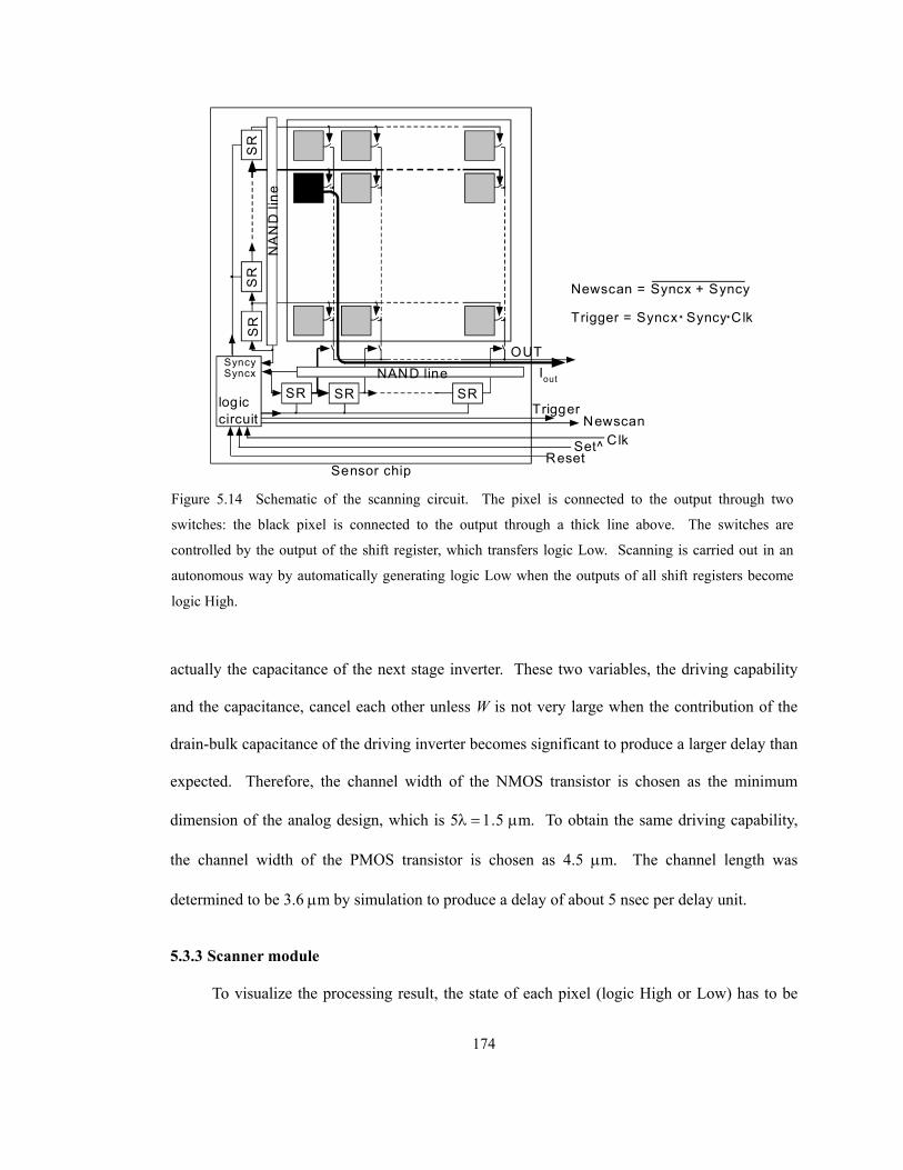
174
actually the capacitance of the next stage inverter. These two variables, the driving capability
and the capacitance, cancel each other unless W is not very large when the contribution of the
drain-bulk capacitance of the driving inverter becomes significant to produce a larger delay than
expected. Therefore, the channel width of the NMOS transistor is chosen as the minimum
dimension of the analog design, which is 5λ = 1.5 µm. To obtain the same driving capability,
the channel width of the PMOS transistor is chosen as 4.5 µm. The channel length was
determined to be 3.6 µm by simulation to produce a delay of about 5 nsec per delay unit.
5.3.3 Scanner module
To visualize the processing result, the state of each pixel (logic High or Low) has to be
SR SR
SR
SR
SR
logiccircuit
Sensor chip
SRTrigger
Newscan
NAND line
NA
ND
line
Set^Reset
Iout
C lk
SyncySyncx
Newscan = Syncx + Syncy
Trigger = Syncx Syncy Clk
OUT
Figure 5.14 Schematic of the scanning circuit. The pixel is connected to the output through two
switches: the black pixel is connected to the output through a thick line above. The switches are
controlled by the output of the shift register, which transfers logic Low. Scanning is carried out in an
autonomous way by automatically generating logic Low when the outputs of all shift registers become
logic High.
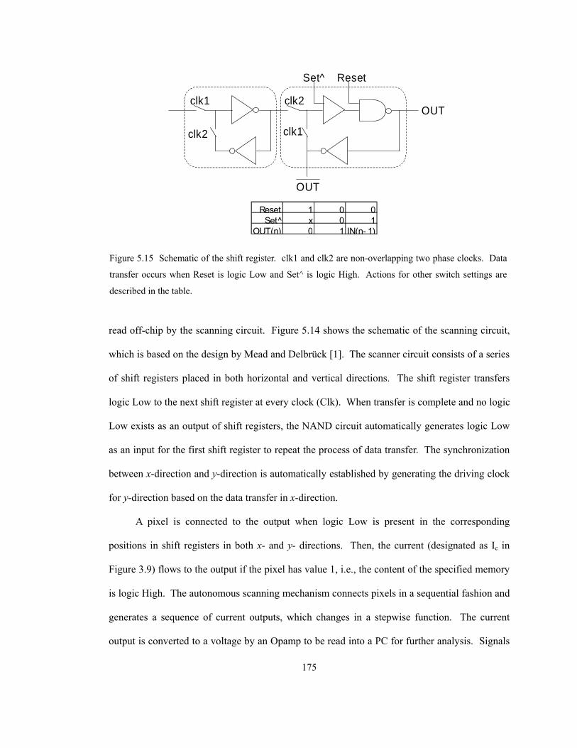
175
read off-chip by the scanning circuit. Figure 5.14 shows the schematic of the scanning circuit,
which is based on the design by Mead and Delbrück [1]. The scanner circuit consists of a series
of shift registers placed in both horizontal and vertical directions. The shift register transfers
logic Low to the next shift register at every clock (Clk). When transfer is complete and no logic
Low exists as an output of shift registers, the NAND circuit automatically generates logic Low
as an input for the first shift register to repeat the process of data transfer. The synchronization
between x-direction and y-direction is automatically established by generating the driving clock
for y-direction based on the data transfer in x-direction.
A pixel is connected to the output when logic Low is present in the corresponding
positions in shift registers in both x- and y- directions. Then, the current (designated as Ic in
Figure 3.9) flows to the output if the pixel has value 1, i.e., the content of the specified memory
is logic High. The autonomous scanning mechanism connects pixels in a sequential fashion and
generates a sequence of current outputs, which changes in a stepwise function. The current
output is converted to a voltage by an Opamp to be read into a PC for further analysis. Signals
clk1
clk1clk2
clk2OUT
Set^ Reset
OUT
Reset 1 0 0Set^ x 0 1
OUT(n) 0 1 IN(n- 1)
Figure 5.15 Schematic of the shift register. clk1 and clk2 are non-overlapping two phase clocks. Data
transfer occurs when Reset is logic Low and Set^ is logic High. Actions for other switch settings are
described in the table.

176
Newscan and Trigger are used for synchronization with the data acquisition system. Signal
Newscan produces a High pulse, indicating the beginning of one frame, followed by a sequence
of Trigger pulses. The data sampling is performed at the rising edge of Trigger pulses.
The schematic of the shift register is shown in Figure 5.15. It is a modified version of a
basic configuration that consists of two semi-static memories connected in a series. Suppose for
the moment that Set^ is logic High and Reset is Low. In this case, the second half of the circuit
reduces to the normal semi-static memory. A pair of clock (clk1, clk2), where clk1 and clk2 are
mutually non-overlapping clocks, transfers data from IN to OUT.
The output can be forced to logic High or logic Low by a combination of Reset and Set^
signals. When both Reset and Set^ are logic Low, signal OUT is logic High. When Reset is
logic High, signal OUT is logic Low regardless of the value of Set^. This resetting function,
which forces the output of all shift registers to logic Low, selects all pixels (remember that logic
Low is an active signal for the selection of a pixel) and hence the current from each pixel is
summed at the output. Therefore, the output current is proportional to the number of pixels of
value 1. This type of output is useful when the position of pixels of value 1 is not important and
the number of these pixels is important instead.
5.4 Layout and chip fabrication
After the entire circuit operation was confirmed by the Hspice simulator, all the circuits
were laid out. Figure 5.16 shows the layout of the pixel. Care was taken to make the pixel
shape square-like to have an equal number of pixels in both x- and y- directions. The pixel size
measures 154.5 µm × 153.3 µm. The phototransistor, which is implemented at the top left
corner of the pixel, measures 99.6 µm × 29.7 µm (base area) and accounts for 12.5% of the
entire pixel area. The transistor accounts for 32.4 % of the pixel area. The rest of the pixel,
which consumes more than half the entire area, was used for the common signal lines, which
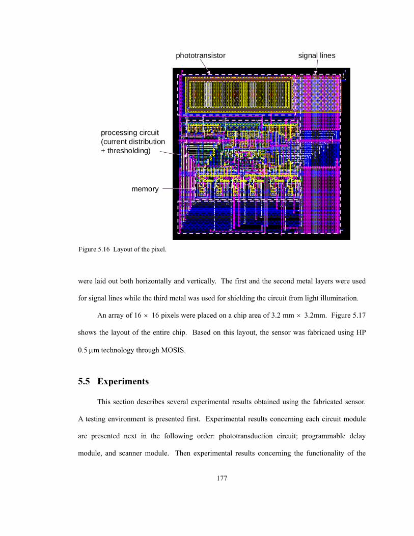
177
were laid out both horizontally and vertically. The first and the second metal layers were used
for signal lines while the third metal was used for shielding the circuit from light illumination.
An array of 16 × 16 pixels were placed on a chip area of 3.2 mm × 3.2mm. Figure 5.17
shows the layout of the entire chip. Based on this layout, the sensor was fabricaed using HP
0.5 µm technology through MOSIS.
5.5 Experiments
This section describes several experimental results obtained using the fabricated sensor.
A testing environment is presented first. Experimental results concerning each circuit module
are presented next in the following order: phototransduction circuit; programmable delay
module, and scanner module. Then experimental results concerning the functionality of the
phototransistor
processing circuit(current distribution+ thresholding)
memory
signal lines
Figure 5.16 Layout of the pixel.
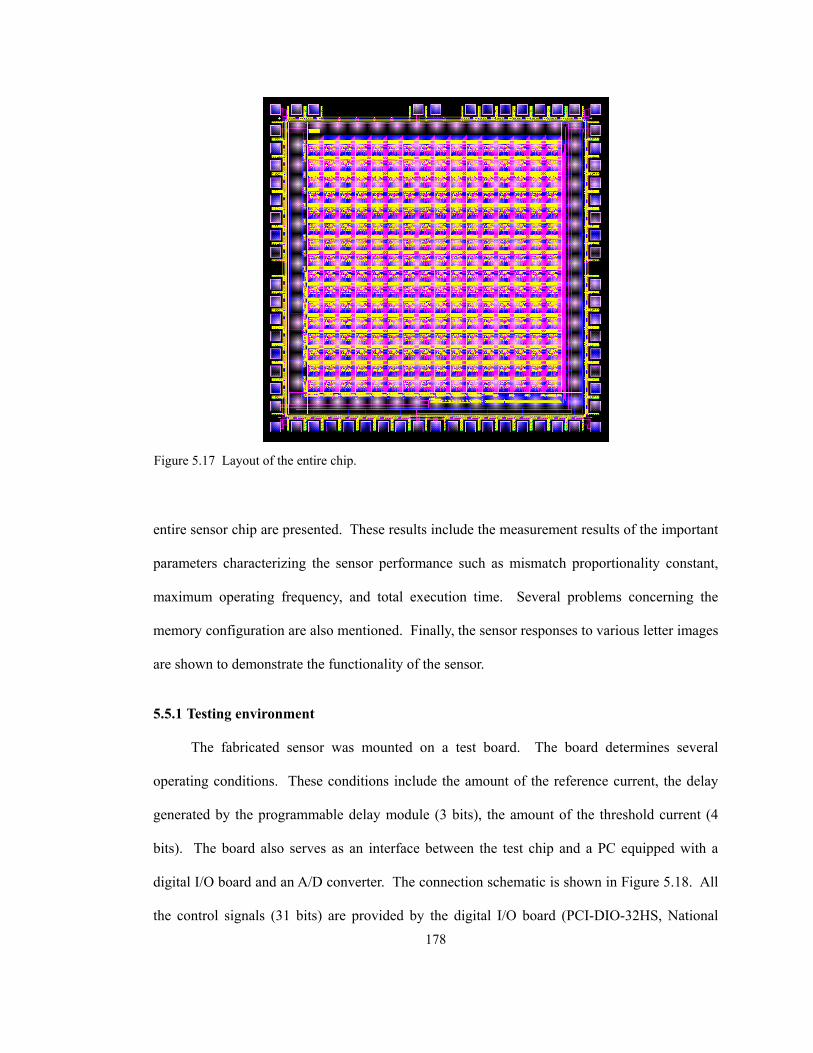
178
entire sensor chip are presented. These results include the measurement results of the important
parameters characterizing the sensor performance such as mismatch proportionality constant,
maximum operating frequency, and total execution time. Several problems concerning the
memory configuration are also mentioned. Finally, the sensor responses to various letter images
are shown to demonstrate the functionality of the sensor.
5.5.1 Testing environment
The fabricated sensor was mounted on a test board. The board determines several
operating conditions. These conditions include the amount of the reference current, the delay
generated by the programmable delay module (3 bits), the amount of the threshold current (4
bits). The board also serves as an interface between the test chip and a PC equipped with a
digital I/O board and an A/D converter. The connection schematic is shown in Figure 5.18. All
the control signals (31 bits) are provided by the digital I/O board (PCI-DIO-32HS, National
Figure 5.17 Layout of the entire chip.
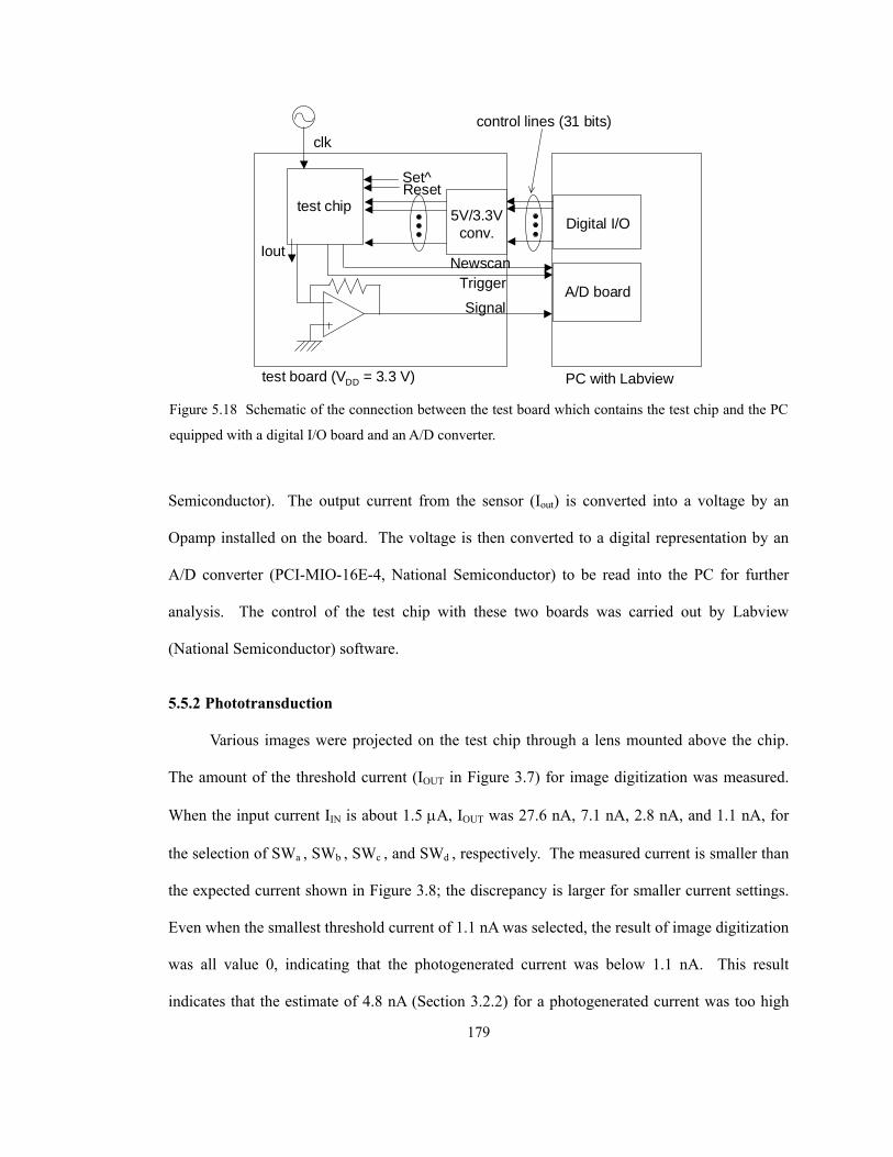
179
Semiconductor). The output current from the sensor (Iout) is converted into a voltage by an
Opamp installed on the board. The voltage is then converted to a digital representation by an
A/D converter (PCI-MIO-16E-4, National Semiconductor) to be read into the PC for further
analysis. The control of the test chip with these two boards was carried out by Labview
(National Semiconductor) software.
5.5.2 Phototransduction
Various images were projected on the test chip through a lens mounted above the chip.
The amount of the threshold current (IOUT in Figure 3.7) for image digitization was measured.
When the input current IIN is about 1.5 µA, IOUT was 27.6 nA, 7.1 nA, 2.8 nA, and 1.1 nA, for
the selection of SWa , SWb , SWc , and SWd , respectively. The measured current is smaller than
the expected current shown in Figure 3.8; the discrepancy is larger for smaller current settings.
Even when the smallest threshold current of 1.1 nA was selected, the result of image digitization
was all value 0, indicating that the photogenerated current was below 1.1 nA. This result
indicates that the estimate of 4.8 nA (Section 3.2.2) for a photogenerated current was too high
test board (VDD = 3.3 V)
Digital I/O
A/D board
PC with Labview
NewscanTrigger
Signal
Iout
clk
test chip
Set^Reset
5V/3.3Vconv.
control lines (31 bits)
Figure 5.18 Schematic of the connection between the test board which contains the test chip and the PC
equipped with a digital I/O board and an A/D converter.
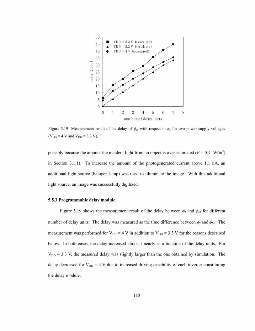
180
possibly because the amount the incident light from an object is over-estimated (E = 0.1 [W/m2]
in Section 3.1.1). To increase the amount of the photogenerated current above 1.1 nA, an
additional light source (halogen lamp) was used to illuminate the image. With this additional
light source, an image was successfully digitized.
5.5.3 Programmable delay module
Figure 5.19 shows the measurement result of the delay between φ2 and φ2d for different
number of delay units. The delay was measured as the time difference between φ2 and φ2d. The
measurement was performed for VDD = 4 V in addition to VDD = 3.3 V for the reasons described
below. In both cases, the delay increased almost linearly as a function of the delay units. For
VDD = 3.3 V, the measured delay was slightly larger than the one obtained by simulation. The
delay decreased for VDD = 4 V due to increased driving capability of each inverter constituting
the delay module.
0
5
10
15
20
25
30
35
40
45
50
0 1 2 3 4 5 6 7 8
num ber of delay units
delay (nsec)
VD D = 3.3 V (m easured)VD D = 3.3 V (sim ulated)VD D = 4 V (m easured)
Figure 5.19 Measurement result of the delay of φ2d with respect to φ2 for two power supply voltages
(VDD = 4 V and VDD = 3.3 V).
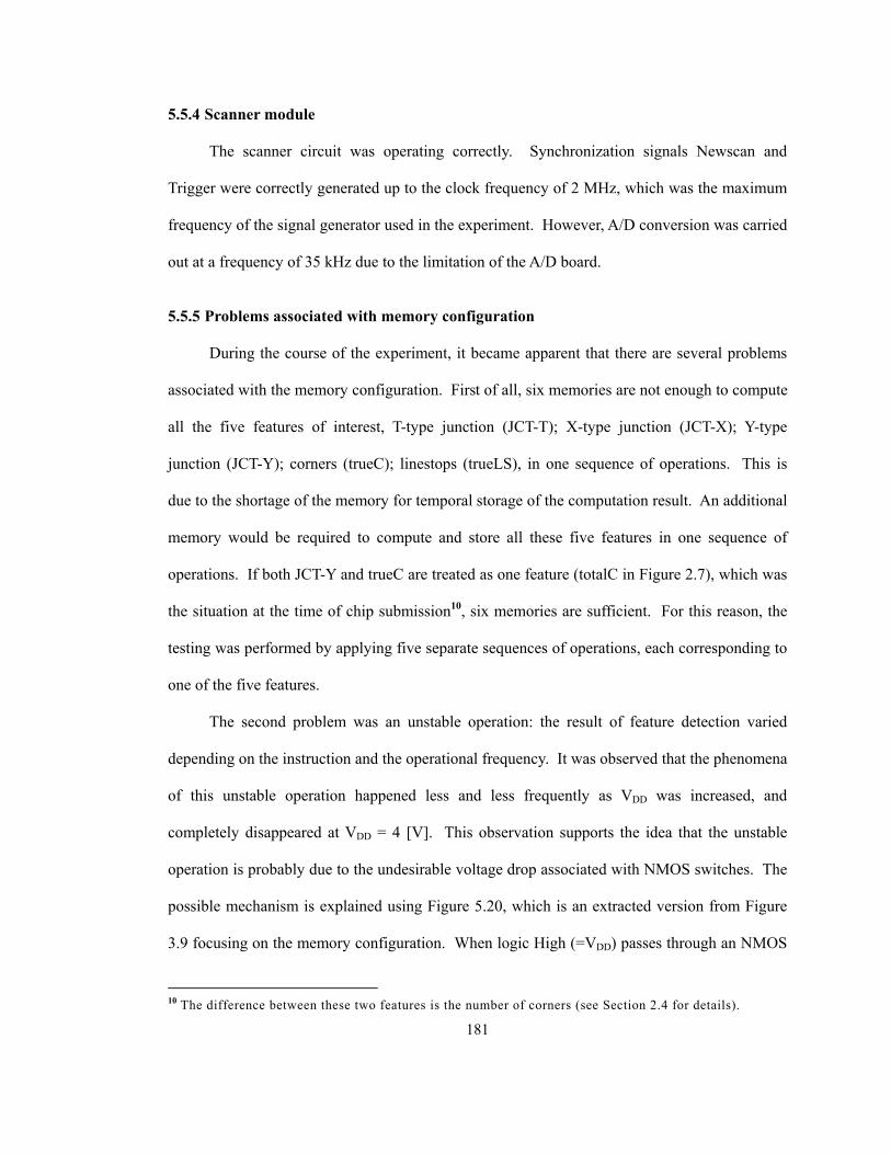
181
5.5.4 Scanner module
The scanner circuit was operating correctly. Synchronization signals Newscan and
Trigger were correctly generated up to the clock frequency of 2 MHz, which was the maximum
frequency of the signal generator used in the experiment. However, A/D conversion was carried
out at a frequency of 35 kHz due to the limitation of the A/D board.
5.5.5 Problems associated with memory configuration
During the course of the experiment, it became apparent that there are several problems
associated with the memory configuration. First of all, six memories are not enough to compute
all the five features of interest, T-type junction (JCT-T); X-type junction (JCT-X); Y-type
junction (JCT-Y); corners (trueC); linestops (trueLS), in one sequence of operations. This is
due to the shortage of the memory for temporal storage of the computation result. An additional
memory would be required to compute and store all these five features in one sequence of
operations. If both JCT-Y and trueC are treated as one feature (totalC in Figure 2.7), which was
the situation at the time of chip submission10, six memories are sufficient. For this reason, the
testing was performed by applying five separate sequences of operations, each corresponding to
one of the five features.
The second problem was an unstable operation: the result of feature detection varied
depending on the instruction and the operational frequency. It was observed that the phenomena
of this unstable operation happened less and less frequently as VDD was increased, and
completely disappeared at VDD = 4 [V]. This observation supports the idea that the unstable
operation is probably due to the undesirable voltage drop associated with NMOS switches. The
possible mechanism is explained using Figure 5.20, which is an extracted version from Figure
3.9 focusing on the memory configuration. When logic High (=VDD) passes through an NMOS
10 The difference between these two features is the number of corners (see Section 2.4 for details).
182
switch (M4a, for example), a voltage drop of about 1 V occurs, decreasing the level of logic
High from 3.3 V to 2.3 V for V4a. This voltage further decreases when M4a gets turned off due
to the inflow of electrons expelled from under the gate. The reduced voltage V4a is transferred
into the memory. If the voltage at the input of the inverter becomes below 1.15 V, which is the
threshold voltage of the inverter, an erroneous result is produced. The problem of the voltage
drop can be avoided in future designs by putting a PMOS transistor in parallel with a NMOS
transistor for the switch.
The third problem is related to the use of y2. Consider the following case: the content of
Ma is used for a certain operation and the operational result (V0 or equivalently V2) is saved to
memory My by setting y2 to logic High. The content of memory Ma should not be altered by
this action. This is achieved by asserting y2, which disconnects Ma from voltage V2. However
in reality, memory Ma is updated with V3, which is the previous operation result, since a1 is
a1
y2
φ2 φ1
Ma
b1
c1
d1
Mb
Mc
Md
V4a
V4b
V4c
V4d
M4a
M4b
M4c
M4d
V3
M3
Vo
V1V2
Figure 5.20 Schematic showing the signal transfer from the thresholding node to the memory. This
figure is an extracted version from Figure 3.9 focusing on the memory configuration.
183
logic High. There is no guarantee that the logic value of V3 is equal to the content of Ma. This
problem is solved by performing a dummy operation before the intended operation. The
dummy operation reads the content and writes it back to memory Ma by asserting signals a1 and
RE (shown in Figure 3.9), automatically presetting V3 to the logic value in memory Ma.
An even more serious problem associated with the use of y2 was signal mixing when
multiple memories are selected as the source of the operation. One of the examples of this type
of operation is the OR operation:
)MMMM(M dcba5.0,y +++= ET . (5.8)
The voltages V4a, V4b, V4c, V4d, corresponding to the memory content, get mixed with each other
to generate a new voltage V3, which is then written into all these four memories. The signal
mixing occurs due to the presence of the common node for the four memories. The above
mentioned method of presetting V3 is effective only when a single memory is addressed and
cannot be used for the case of addressing multiple memories. To get around this problem,
operations addressing multiple memories were executed in several steps, addressing a single
memory in each step, using Mx as a temporary memory.
Although the problems described above concerning the memory configuration
necessitated the use of VDD=4 [V] and slight modification for the operational sequence, they
were not considered fatal to prevent the evaluation of the fabricated sensor.
5.5.6 Pattern generation
For the evaluation of the sensor performance, capability of generating an arbitrary image
pattern by some means is desirable since optically generating an arbitrary image is not a very
flexible method. The ideal method would be to edit an image in a PC and load it into the sensor.
However, the present sensor does not have this function and hence the alternative method was
implemented.
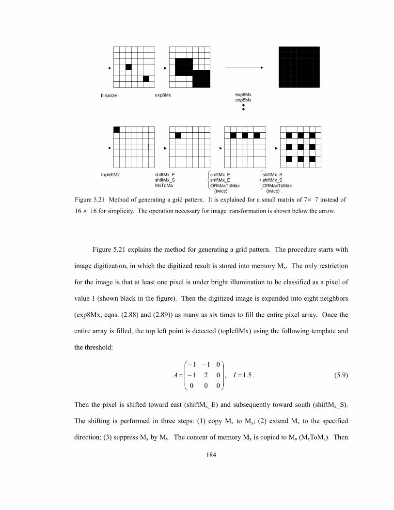
184
Figure 5.21 explains the method for generating a grid pattern. The procedure starts with
image digitization, in which the digitized result is stored into memory Mx. The only restriction
for the image is that at least one pixel is under bright illumination to be classified as a pixel of
value 1 (shown black in the figure). Then the digitized image is expanded into eight neighbors
(exp8Mx, eqns. (2.88) and (2.89)) as many as six times to fill the entire pixel array. Once the
entire array is filled, the top left point is detected (topleftMx) using the following template and
the threshold:
5.1,000021011
=
−
−−= IA . (5.9)
Then the pixel is shifted toward east (shiftMx_E) and subsequently toward south (shiftMx_S).
The shifting is performed in three steps: (1) copy Mx to My; (2) extend Mx to the specified
direction; (3) suppress Mx by My. The content of memory Mx is copied to Ma (MxToMa). Then
exp8Mx exp8Mxexp8Mx
shiftMx_EshiftMx_SMxToMa
shiftMx_EshiftMx_EORMaxToMax (twice)
binarize
topleftMx shiftMx_SshiftMx_SORMaxToMax (twice)
Figure 5.21 Method of generating a grid pattern. It is explained for a small matrix of 7× 7 instead of
16 × 16 for simplicity. The operation necessary for image transformation is shown below the arrow.
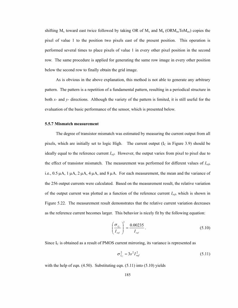
185
shifting Mx toward east twice followed by taking OR of Mx and Ma (ORMaxToMax) copies the
pixel of value 1 to the position two pixels east of the present position. This operation is
performed several times to place pixels of value 1 in every other pixel position in the second
row. The same procedure is applied for generating the same row image in every other position
below the second row to finally obtain the grid image.
As is obvious in the above explanation, this method is not able to generate any arbitrary
pattern. The pattern is a repetition of a fundamental pattern, resulting in a periodical structure in
both x- and y- directions. Although the variety of the pattern is limited, it is still useful for the
evaluation of the basic performance of the sensor, which is presented below.
5.5.7 Mismatch measurement
The degree of transistor mismatch was estimated by measuring the current output from all
pixels, which are initially set to logic High. The current output (IC in Figure 3.9) should be
ideally equal to the reference current Iref. However, the output varies from pixel to pixel due to
the effect of transistor mismatch. The measurement was performed for different values of Iref,
i.e., 0.5 µA, 1 µA, 2 µA, 4 µA, and 8 µA. For each measurement, the mean and the variance of
the 256 output currents were calculated. Based on the measurement result, the relative variation
of the output current was plotted as a function of the reference current Iref, which is shown in
Figure 5.22. The measurement result demonstrates that the relative current variation decreases
as the reference current becomes larger. This behavior is nicely fit by the following equation:
refref
I
IIC 00235.0
2
=
σ. (5.10)
Since IC is obtained as a result of PMOS current mirroring, its variance is represented as
222 3 refI IsC
=σ (5.11)
with the help of eqn. (4.50). Substituting eqn. (5.11) into (5.10) yields
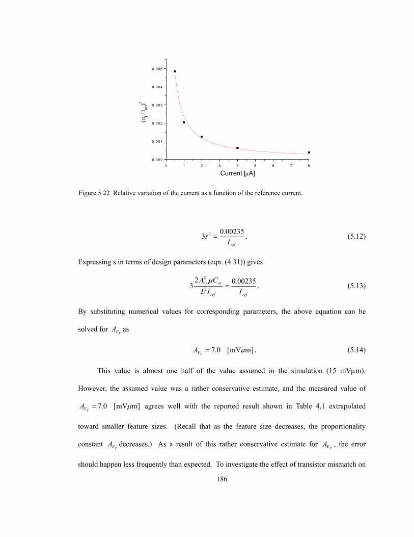
186
refI
s 00235.03 2 = . (5.12)
Expressing s in terms of design parameters (eqn. (4.31)) gives
refref
oxV
IILCA
T 00235.023 2
2
=µ
. (5.13)
By substituting numerical values for corresponding parameters, the above equation can be
solved for TVA as
]mmV[0.7 µ=TVA . (5.14)
This value is almost one half of the value assumed in the simulation (15 mVµm).
However, the assumed value was a rather conservative estimate, and the measured value of
]mmV[0.7 µ=TVA agrees well with the reported result shown in Table 4.1 extrapolated
toward smaller feature sizes. (Recall that as the feature size decreases, the proportionality
constant TVA decreases.) As a result of this rather conservative estimate for
TVA , the error
should happen less frequently than expected. To investigate the effect of transistor mismatch on
0 1 2 3 4 5 6 7 80. 000
0. 001
0. 002
0. 003
0. 004
0. 005
(σΙ /
Ι ref)2
Current [µA]
Figure 5.22 Relative variation of the current as a function of the reference current.
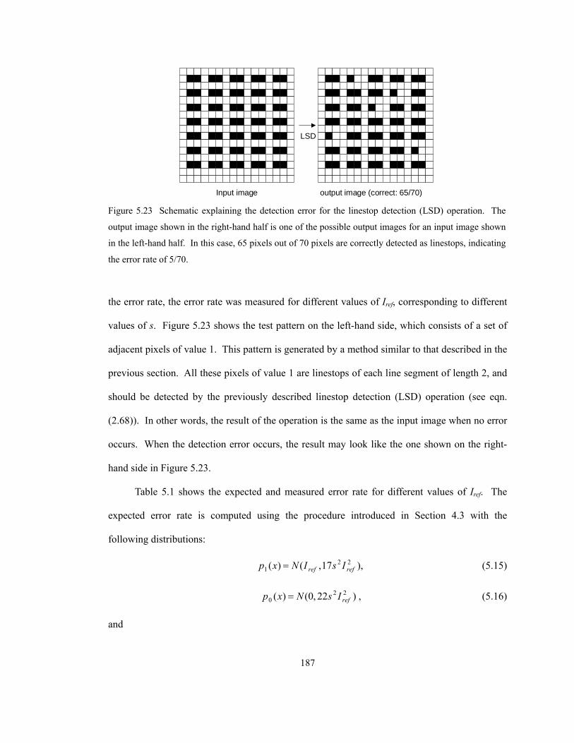
187
the error rate, the error rate was measured for different values of Iref, corresponding to different
values of s. Figure 5.23 shows the test pattern on the left-hand side, which consists of a set of
adjacent pixels of value 1. This pattern is generated by a method similar to that described in the
previous section. All these pixels of value 1 are linestops of each line segment of length 2, and
should be detected by the previously described linestop detection (LSD) operation (see eqn.
(2.68)). In other words, the result of the operation is the same as the input image when no error
occurs. When the detection error occurs, the result may look like the one shown on the right-
hand side in Figure 5.23.
Table 5.1 shows the expected and measured error rate for different values of Iref. The
expected error rate is computed using the procedure introduced in Section 4.3 with the
following distributions:
),17,()( 221 refref IsINxp = (5.15)
)22,0()( 220 refIsNxp = , (5.16)
and
LSD
Input image output image (correct: 65/70) Figure 5.23 Schematic explaining the detection error for the linestop detection (LSD) operation. The
output image shown in the right-hand half is one of the possible output images for an input image shown
in the left-hand half. In this case, 65 pixels out of 70 pixels are correctly detected as linestops, indicating
the error rate of 5/70.
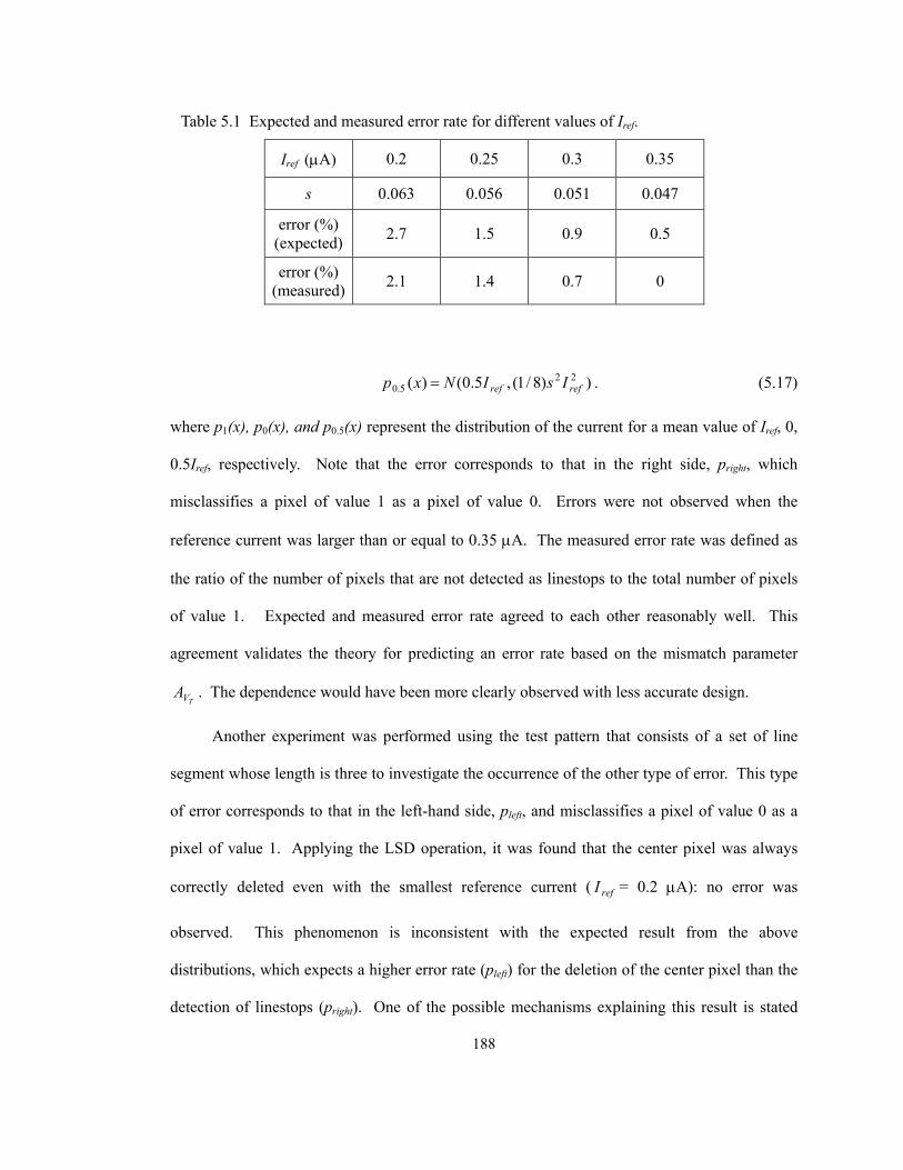
188
))8/1(,5.0()( 225.0 refref IsINxp = . (5.17)
where p1(x), p0(x), and p0.5(x) represent the distribution of the current for a mean value of Iref, 0,
0.5Iref, respectively. Note that the error corresponds to that in the right side, pright, which
misclassifies a pixel of value 1 as a pixel of value 0. Errors were not observed when the
reference current was larger than or equal to 0.35 µA. The measured error rate was defined as
the ratio of the number of pixels that are not detected as linestops to the total number of pixels
of value 1. Expected and measured error rate agreed to each other reasonably well. This
agreement validates the theory for predicting an error rate based on the mismatch parameter
TVA . The dependence would have been more clearly observed with less accurate design.
Another experiment was performed using the test pattern that consists of a set of line
segment whose length is three to investigate the occurrence of the other type of error. This type
of error corresponds to that in the left-hand side, pleft, and misclassifies a pixel of value 0 as a
pixel of value 1. Applying the LSD operation, it was found that the center pixel was always
correctly deleted even with the smallest reference current ( refI = 0.2 µA): no error was
observed. This phenomenon is inconsistent with the expected result from the above
distributions, which expects a higher error rate (pleft) for the deletion of the center pixel than the
detection of linestops (pright). One of the possible mechanisms explaining this result is stated
Table 5.1 Expected and measured error rate for different values of Iref.
Iref (µA) 0.2 0.25 0.3 0.35
s 0.063 0.056 0.051 0.047
error (%) (expected) 2.7 1.5 0.9 0.5
error (%) (measured) 2.1 1.4 0.7 0
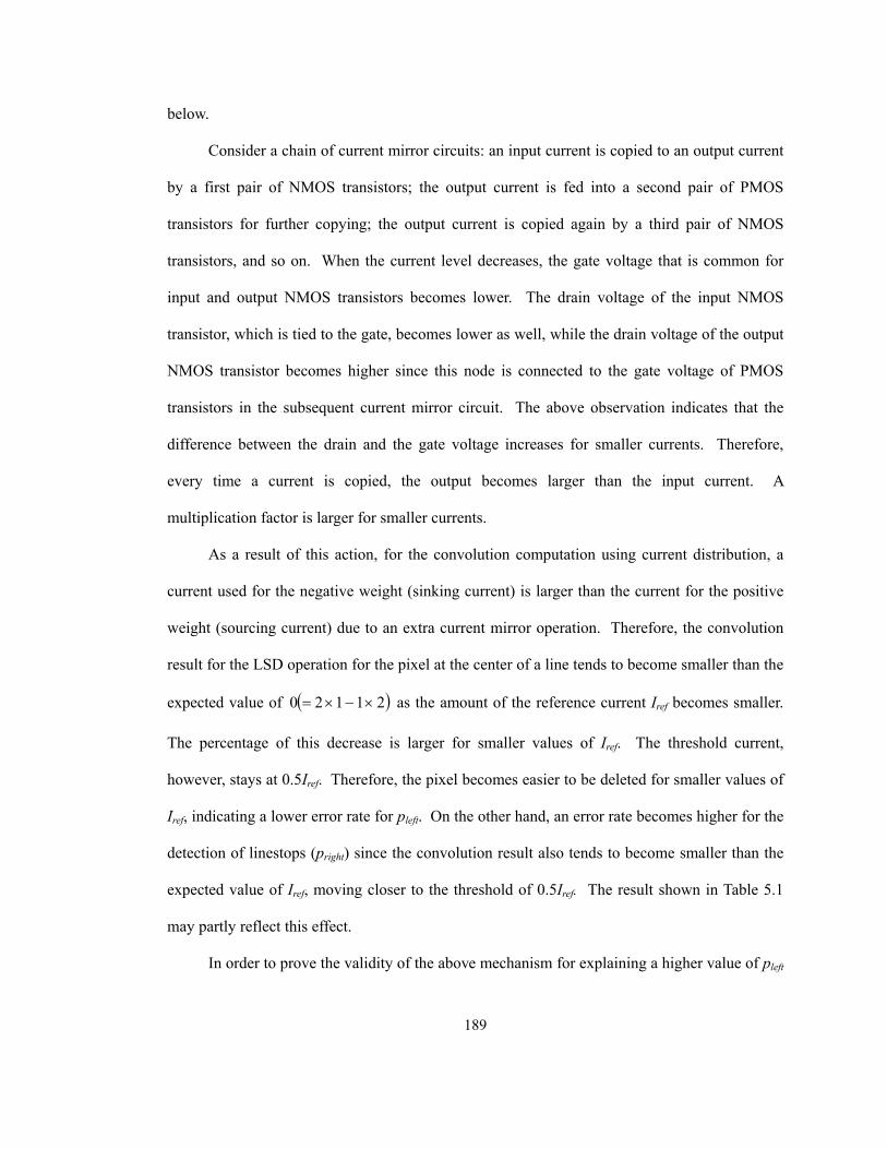
189
below.
Consider a chain of current mirror circuits: an input current is copied to an output current
by a first pair of NMOS transistors; the output current is fed into a second pair of PMOS
transistors for further copying; the output current is copied again by a third pair of NMOS
transistors, and so on. When the current level decreases, the gate voltage that is common for
input and output NMOS transistors becomes lower. The drain voltage of the input NMOS
transistor, which is tied to the gate, becomes lower as well, while the drain voltage of the output
NMOS transistor becomes higher since this node is connected to the gate voltage of PMOS
transistors in the subsequent current mirror circuit. The above observation indicates that the
difference between the drain and the gate voltage increases for smaller currents. Therefore,
every time a current is copied, the output becomes larger than the input current. A
multiplication factor is larger for smaller currents.
As a result of this action, for the convolution computation using current distribution, a
current used for the negative weight (sinking current) is larger than the current for the positive
weight (sourcing current) due to an extra current mirror operation. Therefore, the convolution
result for the LSD operation for the pixel at the center of a line tends to become smaller than the
expected value of ( )21120 ×−×= as the amount of the reference current Iref becomes smaller.
The percentage of this decrease is larger for smaller values of Iref. The threshold current,
however, stays at 0.5Iref. Therefore, the pixel becomes easier to be deleted for smaller values of
Iref, indicating a lower error rate for pleft. On the other hand, an error rate becomes higher for the
detection of linestops (pright) since the convolution result also tends to become smaller than the
expected value of Iref, moving closer to the threshold of 0.5Iref. The result shown in Table 5.1
may partly reflect this effect.
In order to prove the validity of the above mechanism for explaining a higher value of pleft
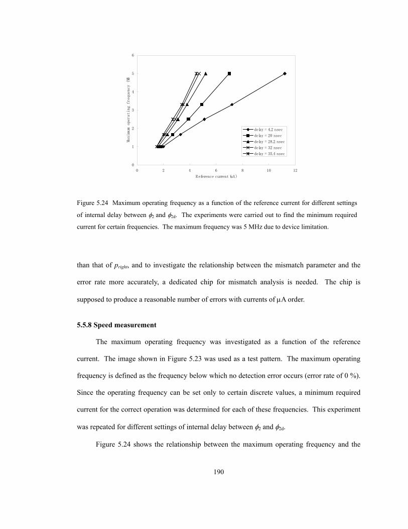
190
than that of pright, and to investigate the relationship between the mismatch parameter and the
error rate more accurately, a dedicated chip for mismatch analysis is needed. The chip is
supposed to produce a reasonable number of errors with currents of µA order.
5.5.8 Speed measurement
The maximum operating frequency was investigated as a function of the reference
current. The image shown in Figure 5.23 was used as a test pattern. The maximum operating
frequency is defined as the frequency below which no detection error occurs (error rate of 0 %).
Since the operating frequency can be set only to certain discrete values, a minimum required
current for the correct operation was determined for each of these frequencies. This experiment
was repeated for different settings of internal delay between φ2 and φ2d.
Figure 5.24 shows the relationship between the maximum operating frequency and the
0
1
2
3
4
5
6
0 2 4 6 8 10 12
Reference current (uA)
Maximum operating frequency (MH
delay = 4.2 nsec
delay = 20 nsec
delay = 28.2 nsec
delay = 32 nsec
delay = 35.4 nsec
Figure 5.24 Maximum operating frequency as a function of the reference current for different settings
of internal delay between φ2 and φ2d. The experiments were carried out to find the minimum required
current for certain frequencies. The maximum frequency was 5 MHz due to device limitation.
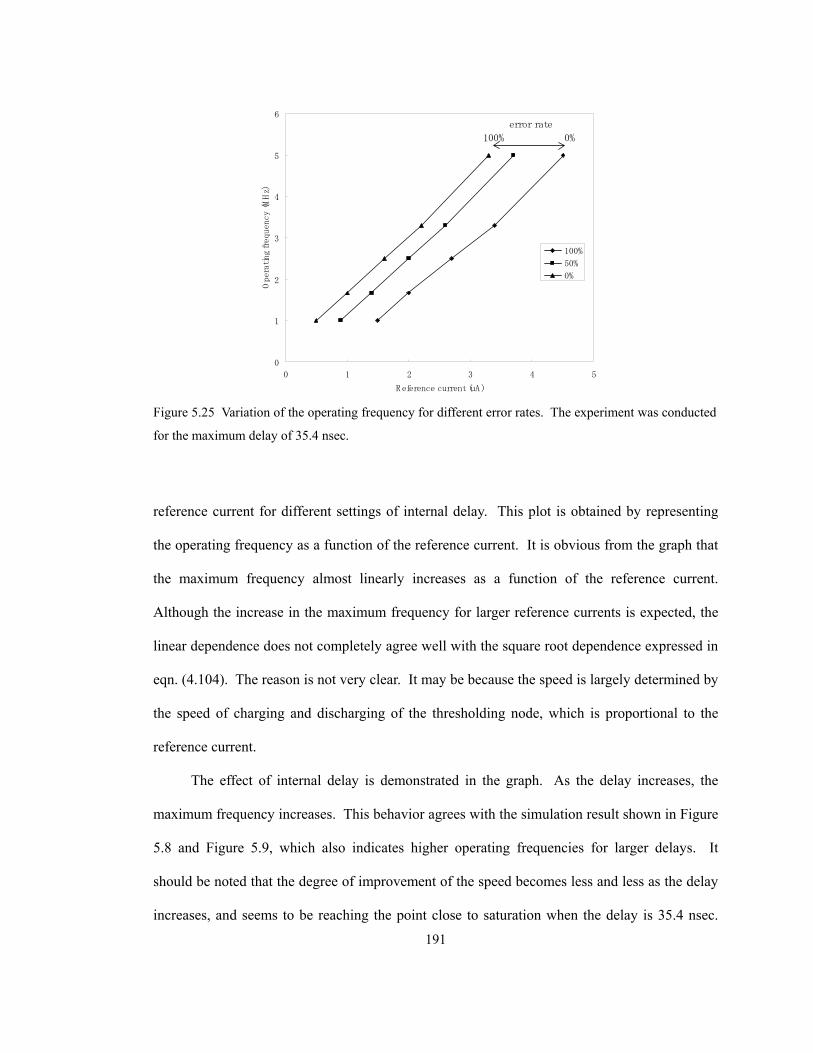
191
reference current for different settings of internal delay. This plot is obtained by representing
the operating frequency as a function of the reference current. It is obvious from the graph that
the maximum frequency almost linearly increases as a function of the reference current.
Although the increase in the maximum frequency for larger reference currents is expected, the
linear dependence does not completely agree well with the square root dependence expressed in
eqn. (4.104). The reason is not very clear. It may be because the speed is largely determined by
the speed of charging and discharging of the thresholding node, which is proportional to the
reference current.
The effect of internal delay is demonstrated in the graph. As the delay increases, the
maximum frequency increases. This behavior agrees with the simulation result shown in Figure
5.8 and Figure 5.9, which also indicates higher operating frequencies for larger delays. It
should be noted that the degree of improvement of the speed becomes less and less as the delay
increases, and seems to be reaching the point close to saturation when the delay is 35.4 nsec.
0
1
2
3
4
5
6
0 1 2 3 4 5
Reference current (uA)
Operating frequency (MHz)
100%
50%
0%
0%100%
error rate
Figure 5.25 Variation of the operating frequency for different error rates. The experiment was conducted
for the maximum delay of 35.4 nsec.
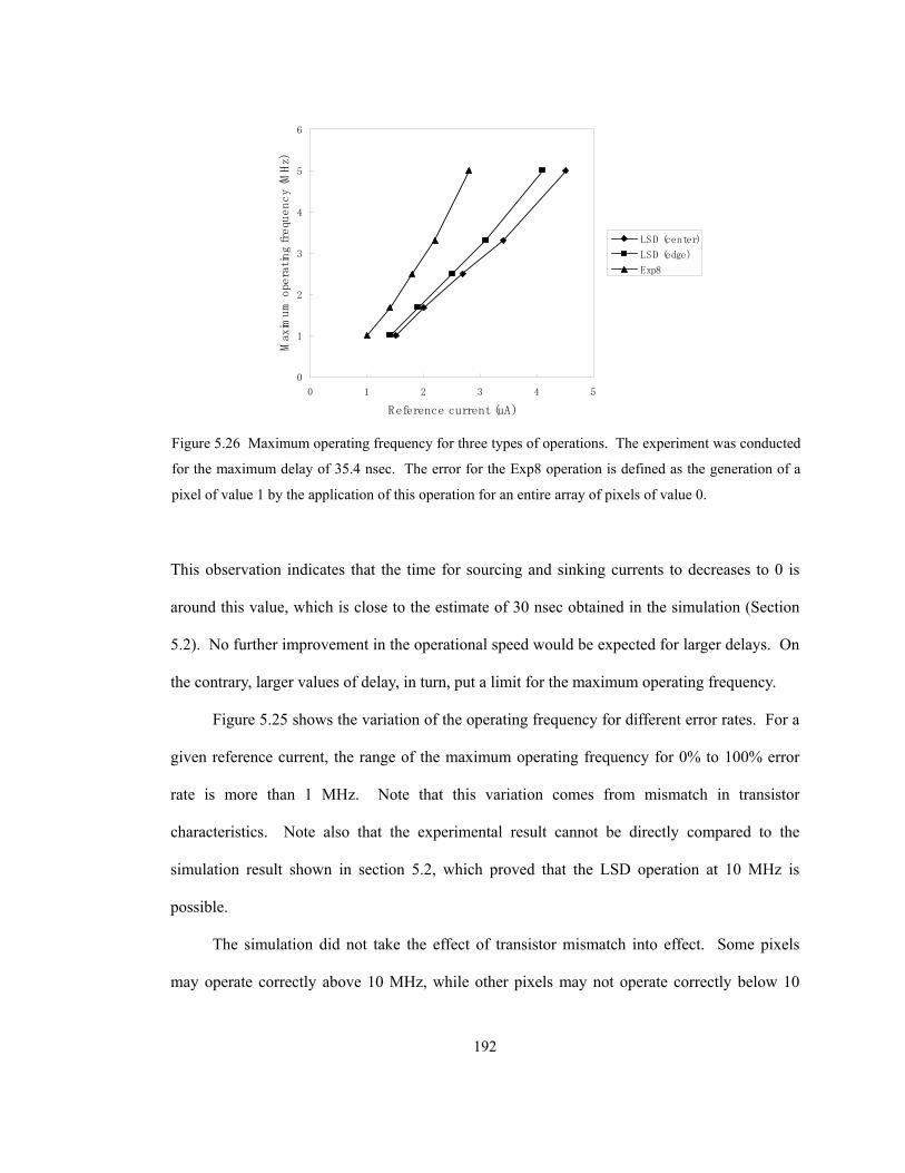
192
This observation indicates that the time for sourcing and sinking currents to decreases to 0 is
around this value, which is close to the estimate of 30 nsec obtained in the simulation (Section
5.2). No further improvement in the operational speed would be expected for larger delays. On
the contrary, larger values of delay, in turn, put a limit for the maximum operating frequency.
Figure 5.25 shows the variation of the operating frequency for different error rates. For a
given reference current, the range of the maximum operating frequency for 0% to 100% error
rate is more than 1 MHz. Note that this variation comes from mismatch in transistor
characteristics. Note also that the experimental result cannot be directly compared to the
simulation result shown in section 5.2, which proved that the LSD operation at 10 MHz is
possible.
The simulation did not take the effect of transistor mismatch into effect. Some pixels
may operate correctly above 10 MHz, while other pixels may not operate correctly below 10
0
1
2
3
4
5
6
0 1 2 3 4 5
Reference current (uA)
Maximum operating frequency (M
Hz)
LS D (center)
LSD (edge)
Exp8
Figure 5.26 Maximum operating frequency for three types of operations. The experiment was conducted
for the maximum delay of 35.4 nsec. The error for the Exp8 operation is defined as the generation of a
pixel of value 1 by the application of this operation for an entire array of pixels of value 0.

193
MHz, depending on the degree of mismatch within a 33× region including itself and
neighbors. The other difference between the simulation and the experiment is the edge effect.
The linestops detected in the simulation is located at the edge. Since three pixels are missing in
its neighbors, the detection should be easier for pixels on the edge than those at the center11,
which is actually the case for experiment.
The effect of the type of operations on the maximum operating frequency was also
investigated. These operations include the LSD operation (TLSD4) on the edge and the Exp8
operation (Texp8). The error for the Exp8 operation is defined as the generation of pixels of value
1 by the application of this operation for an entire array of pixels of value 0. Figure 5.26 shows
the maximum operating frequency for these operations as well as the LSD operation at the
center, which is already shown in Figure 5.24. The maximum frequency is lowest for the LSD
operation at the center: this operation needs a largest current at a given frequency for correct
operation. The maximum frequency for the LSD operation at the edge is higher than the LSD
operation at the center. The maximum frequency for the Exp8 operation is significantly higher
than these two LSD operations.
For the other type of error for the Exp8 operation, which produces pixels of value 0 in the
33× neighbors of a pixel of value 1, the maximum operating frequency was even higher. It
seems that the maximum frequency is higher for simpler operations and is lower for complex
operations. It is the expected result since complex operations use more current sources, which
can be either positive or negative, and hence take longer time to obtain the correct result. For
the characterization of the sensor, the maximum operating frequency is defined as 5 MHz with
the reference current of 4.5 µA, using the LSD operation at the center as the worst case.
11 This phenomenon happens due to the precharging of each pixel during preparation phase before the
operation starts. Without this mechanism for high speed operation, there is no difference between the LSD operation at the edge and the LSD operation at the center.

194
5.5.9 Responses to letter images
Various letter images were projected on the feature detection sensor. The experiments
were conducted under the following conditions: VDD = 4 V, Iref = 4.5 µA, the delay between φ2
and φ2d set to 35.4 nsec, the operating frequency of 5 MHz. Figure 5.27 shows detected features
by the sensor for five letter images. The images shown in the bottom row are reconstructed by
superimposing each feature at the detected position on the thinned image. All the important
features were detected in a discriminative fashion. Comparison of these results with the
simulation result (as was done in Section 2.7) showed that the sensor response was completely
identical to the one predicted by the simulation. Prediction by the simulation was carried out
using a digitized image (X0). Note that this process is necessary since the result of image
digitization can be slightly different from the originally prepared image due to illumination
inhomogeneity and edge effects. The identity between the detected results and the simulation
demonstrates that the sensor is functioning as designed.
It was found that some of the results are confusing. For example, for the slanted letter
"R", two pixels are detected as linestops instead of corners. This is because the o45 line
trueLSJC T-T & trueCJC T-XJC T-Y
Figure 5.27 Sensor responses to various letter images. For an input image shown on the top row, a set of
features is obtained as shown in the bottom row. These features are superimposed on the thinned image.
The center of a closed rectangle indicates the position of the detected feature.

195
segment constituting the loop is removed by the EIP operation due to its length being two
pixels. This type of removal of short line segments also explains why only seven corners are
detected instead of eight for the letter “O” and the unexpected linestops along the stroke for the
letter “S”. This problem originates from the low resolution of the sensor: an array of 1616 × is
not large enough for some letters to apply the present feature detection algorithm. Hence, the
problem would be solved if the larger number of pixels were used in future.
Table 5.2 shows the execution time for each operation used for the detection of the
following four features: JCT-T, JCT-X, totalC (OR of trueC and JCT-Y), and trueLS. Note that
trueC and JCT-Y are treated together as totalC in this example. Recall that due to lack of an
Table 5.2 Execution time required for each operation. The result of each processing is
shown as Xi in Figure 5.28. The processing time is estimated for the operation of 5 MHz. order operation resultant image no. of steps time (µsec)
1 binarize X0 1 0.22 thinning (1 cycle) 24 4.83 thinning (1 cycle) X1 24 4.84 OD X2a, X2b, X2c, X2d, 25 55 LC X3a, X3b, X3c, X3d 26 5.26 EIP X4a, X4b, X4c, X4d 20 47 LI X5a, X5b, X5c, X5d 8 1.68 EIP X6a, X6b, X6c, X6d 20 49 LT 2 0.4
10 LE 4 0.811 LT X7a, X7b, X7c, X7d 2 0.412 AND2MabcdToMx X10 29 5.813 LSD X8a, X8b, X8c, X8d 4 0.814 ORMabcdToMy 8 1.615 ORMxyToMy X13 1 0.216 rectangleMy 4 0.817 shrinkMy 4 0.818 connectMy 12 2.419 rectangleMy 4 0.820 rectangleMy X14 4 0.821 shrinkMy X15 4 0.822 LSD1 X9a, X9b, X9c, X9d 8 1.623 ORMabcdToMy X16 8 1.624 AND2MabcdToMabcd X17 1 0.225 rectangleMx X11 4 0.826 shrinkMx X12 4 0.827 feature_calc X18, X19, X20, X21, X22 16 3.2
total 271 54.2
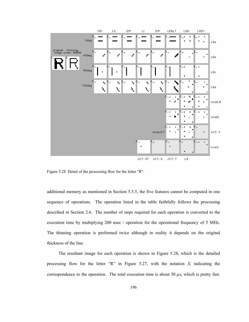
196
additional memory as mentioned in Section 5.5.5, the five features cannot be computed in one
sequence of operations. The operation listed in the table faithfully follows the processing
described in Section 2.6. The number of steps required for each operation is converted to the
execution time by multiplying 200 nsec / operation for the operational frequency of 5 MHz.
The thinning operation is performed twice although in reality it depends on the original
thickness of the line.
The resultant image for each operation is shown in Figure 5.28, which is the detailed
processing flow for the letter “R” in Figure 5.27, with the notation Xi indicating the
correspondence to the operation. The total execution time is about 50 µs, which is pretty fast.
or iginalimage
t h inn ingorder : WSEN
OD LC EIP LI
J C T- XT
EIP
J C T- X
LE<
J C T- T
LSD
LS
LSD1
LSa
LSb
LSc
LSd
t ot alLS
t ot alC
J C T- Y
t rueC
t ot alJ C T
0deg
45deg
90deg
135degdX 9
aX 9
bX 9
cX 9
dX 2
aX 2
bX 2
cX 2
dX 3
aX 3
bX 3
cX 3
dX 4
aX 4
bX 4
cX 4
dX 5
aX 5
bX 5
cX 5
dX 6
aX 6
bX 6
cX 6
dX 7
aX 7
bX 7
cX 7
dX 8
aX 8
bX 8
cX 8
10X
1X
11X
12X
13X
14X
15X
16X
17X
18X
19X 20X 21X 22X 23X
0X
Figure 5.28 Detail of the processing flow for the letter "R".

197
If the memory configuration is modified to solve the problems described in Section 5.5.5, the
twelfth and the fourteenth operations (shaded region in the figure) can be executed in one step
for each of them, which would further reduce the processing time.
5.5.10 Discussion
The fabricated feature detection sensor operated successfully with a fairly high speed.
The operation was confirmed up to 5 MHz with the reference current of 4.5 µA and the power
supply voltage of 4 V. With this setting, the sensor was able to detect features (junctions of
three types, corners, and linestops) in a discriminative fashion for various types of letter images
in about 50 µsec. The detection result was exactly the same as that predicted by simulation.
The mechanism of high speed charging/discharging of the critical node was necessary as well as
the mechanism of temporarily keeping the thresholding node voltage constant in order to
achieve this operational speed. Since the maximum operating frequency is almost linearly
dependent on the reference current, further improvement of the speed is possible by increasing
the reference current within the region for transistors to operate in saturation.
The present sensor has a larger computational power than the one obtained by the sensor
architecture using a single conventional signal processor. Suppose that the processor operates at
the clock frequency of 1 GHz and that each arithmetic computation requires 1 nsec. Also,
suppose that the weighted sum is computed in one clock cycle. These assumptions lead to the
computation time for template matching for 33 × neighbors of 9 nsec, which further lead to the
total computation time of 29N nsec for a pixel array of size NN × . If N is equal to 16, which
is the size of the present sensor, the computation time is 2.3 µsec. This is ten times larger than
the operational speed of 200 nsec obtained from the fabricated sensor at the operating frequency
of 5 MHz. The higher speed of the present sensor comes from the parallel computing due to the
incorporation of the processing element per each pixel. The discrepancy between the two
198
schemes becomes even larger for larger N. The computational time required for a single
processor architecture is proportional to 2N , while that required for the present sensor is
independent of N.
The mismatch proportionality constant TVA was estimated as 7 mV from the variation of
the current output. One of the experimental results suggested the validity of the design
procedure based on the mismatch analysis: the measured error rate was close to the theoretical
prediction. Since the transistor dimension was determined based on the conservative estimate
of TVA , the transistor channel length could be even reduced to satisfy the original accuracy
requirement. The reduced channel length leads to an even faster operation.
The power consumption of the sensor was measured only as a DC current flowing out of
the power supply to GND. The AC current was not measured due to the limitation of the
measurement instrument. The current consumption depends on the number of current paths
between VDD and GND, which is affected by the content of the memories and the specified
operation. The current consumption was always below 20 mA under the normal operating
conditions (VDD = 4 V, Iref = 4.5 µA). It was found that the DC current consumption consists of
two parts: the constant current consumption independent of the reference current and the other
one that is proportional to the reference current. The constant current is consumed by the
inverter while keeping the thresholding node voltage constant during φ2 and φ2d phases.
Although it is not clear how much AC current is consumed, it is reasonable to say that the total
power consumption is around 100 mW.
Table 5.3 summarizes the specifications of the sensor. Employment of the mixed-mode
approach enabled compact implementation of the pixel circuit. Use of technology of smaller
feature sizes enables higher pixel densities in future versions. If the 0.35 µm technology is
used, the pixel size reduces to 100 µm × 100 µm, enabling an array of 64 × 64 pixels in a chip

199
area of 7.2 mm × 7.2 mm. This is a practically useful resolution and is technically feasible to
implement. With the shrinking of the pixel size, the photosensor would have to be implemented
in the integration type since the amount of a photogenerated current from the reduced size of
phototransistor is too small. The change in the configuration of the photosensor would also
expand the application area of the feature detection sensor since it opens up the possibility of
directly dealing with gray-level images.
There are several issues that need future modifications. Insertion of a complementary
PMOS switch is necessary for complete voltage transfer. This would enable chip operation with
the supply voltage of 3.3 V. The problem of signal mixing at the common node for memories
Ma, Mb, Mc, and Md, can be solved by replacing the present y2 switch with four separate
switches and placing each of them between a1 and Ma, b1 and Mb, c1 and Mc, d1 and Md,
respectively.
5.6 Summary
Experimental results using the prototype sensor has been presented as well as some
implementation issues in this chapter. The analysis of the transient behavior of the internal node
led to the implementation of two mechanisms for high-speed operation. The first mechanism
quickly charges and discharges the critical node for current distribution. The second mechanism
Table 5.3 Specifications of the prototype chip.
technology HP 0.5 µm chip area 3.2 mm × 3.2 mm pixel size 16 × 16 pixel area 154.5 µm × 153.3 µm number of transistors 147 / pixel max operating freq.* 5 MHz fill factor (photosensor) 12.5 %
( *measured for VDD = 4 V and Iref = 4.5 µA)
200
keeps the voltage at the thresholding node constant for an additional time period.
A prototype sensor has been fabricated. The sensor contains an array of 16 × 16 pixels,
each measuring 150 µm × 150 µm in a chip area of 3.2 mm × 3.2 mm. The sensor operated
successfully with the power supply voltage of 4 V. The mismatch proportionality constant TVA
was determined as 7 mVµm. With the reference current set to 4.5 µA, the operation was
confirmed up to the frequency of 5 MHz. With these settings, discriminative detection of the
features (junctions of three types, corners, and linestops) was possible in about 50 µsec. No
classification error was observed due to what turned out to be a conservative design. One of the
experimental results suggested the validity of the proposed theory that relates the mismatch
parameter to the error rate.
5.7 References
[1] C. Mead and T. Delbrück, “Scanners for visualizing activity of analog VLSI circuitry,” CNS
MEMO 11, California Institute of Technology, Pasadena, CA, 1991.
201
Chapter 6 Conclusion
This thesis has explored the design and implementation of a new type of VLSI
computational sensor. The sensor detects important image features including corners, three
types of junctions (T-type, X-type, Y-type), and linestops for a binary image in a discriminative
fashion. The sensor contains an array of 1616 × processing elements, each measuring 150 µm
× 150 µm in a chip area of 3.2 mm × 3.2 mm. Since these features are detected on-chip in
about 50 µsec, the sensor can be used for various types of applications requiring high speed.
For the realization of this sensor, several aspects including an algorithm, architectural design,
design procedure based on transistor mismatch, implementation details are investigated and
discussed in the thesis.
In Chapter 2, an algorithm for the feature detection has been described. The algorithm is
inspired by the biological vision system, which performs detection and hierarchical integration
of features. The proposed algorithm first decomposes an input image into four orientations and
detects linestops for line segments in each orientation plane. Corners and junctions are detected
as a result of interaction between line segments and linestops in different orientation planes.
The algorithm is formulated on the basis of template matching which iteratively performs a
33× neighborhood processing.
In Chapter 3, an architectural design of the feature detection sensor has been presented.
An analog/digital mixed-mode configuration is employed to achieve the advantages of both
analog and digital implementations. An input image is digitized first by comparing the steady-
state output of a phototransistor with a threshold current. Then the 33× neighborhood
processing is carried out by the current distribution according to a proper kernel and the
thresholding operation. The computation result is stored into a specified memory to be used for

202
the next operation. The operational sequence can be programmed in a digital fashion.
In Chapter 4, a systematic design procedure for current-mode processing circuits based
on transistor mismatch analysis has been proposed. First, a set of formulas is derived to
represent the current variation as a function of the design parameters (transistor dimension and
the reference current). The formulas also take the configuration of the current mirror circuit
into account. Using these expressions, the proposed method converts the specifications for
accuracy, speed, and the transistor operating condition to the requirement for the design
parameters. These parameters are chosen to satisfy all the above three requirements.
In Chapter 5, implementation details and experimental results using the prototype sensor
have been presented. Two mechanisms for high-speed operation, one for the quick charging and
discharging of the critical node and the other one for keeping the thresholding node voltage
constant for an additional time period, are explained. The response obtained from the sensor
was identical to the simulated result when operated with the power supply voltage of 4 V and
with the operating frequency up to 5 MHz, confirming the functionality of the sensor.
The confirmation of the successful operation of the sensor completes the objective of the
thesis. The sensor is unique by incorporating some flavor of the hierarchical feature integration,
which enables the discriminative detection of the five features on chip. This is the first feature
detection sensor of this kind.
The work presented in this thesis has considerable room for future extensions. Further
improvement of the algorithm is possible by incorporating several methods proposed in the
Discussion section of Chapter 2 However, the fundamental limitation of an interaction area of
33× neighborhood, which is required for feasible wiring in VLSI implementation, would still
exist. The algorithm sometimes suffers from local noise. A certain type of preprocessing which
filters out unnecessary branches or image smoothing may be necessary to further increase the
robustness.
203
As far as the sensor is concerned, incorporation of the edge detection mechanism as a
first-step processing makes the sensor directly applicable to gray-level images, which should
significantly expand the application area of the sensor. Another interesting area to investigate is
the method of scanning the pixel activity. The scanning procedure implemented in the present
sensor sequentially scans pixels, resulting in a large number of values 0 carrying no
information. To fully exploit the advantage of on-chip feature detection, only meaningful
information (pixels of value 1) should be transferred to a host CPU by some mechanism. One
of the possible mechanisms is to skip a pixel of value 0 by modification of the shift register.
Further investigation for the relationship between the transistor mismatch and the
accuracy of the circuit is of interest. A dedicated chip, which is designed to produce large
current variations in a reasonable amount of current, is necessary for this purpose. An even
more challenging but important work is the analysis of the accuracy in a dynamic sense. The
analysis presented in the thesis has represented accuracy in a static sense, which does not
completely reflect reality. Ideally, accuracy should be represented as a function of time. The
analysis gets even more complicated when the speed variation due to transistor mismatch is
taken into account.
As a concluding remark, we hope that the presented work will stimulate further research
activities in the field of computational sensors.

204
Bibliography
A. Andreou, K. Boahen, P. Pouliquen, A. Pavasovic, R. Jenkins, and K. Strohbehn, “Current-
mode subthreshold MOS circuits for analog neural systems,” IEEE Trans. Neural Networks,
vol. 2, no. 2, pp. 205-213, 1991.
C. Aw and B. Wooley, “128× 128-pixel standard-CMOS image sensor with electronic shutter,”
IEEE J. Solid-State Circuits, vol. 31, no. 12, pp. 1922-1930, 1996.
F. Attneave, “Some informational aspects of visual perception,” Psychological Review, vol. 61,
no. 3, pp. 183-193, 1954.
H. S. Baird and I. Guyon, "Neural network recognizer for hand-written zip code digits,"
Advances in Neural Information Processing Systems, (D. Touretzky ed.), vol. 1, Morgan
Kaufman, San Mateo, CA, p. 323-331, 1989.
J. Bastos, M. Steyaert, R. Roovers, P. Kinget, W. Sansen, B. Graindourze, A. Pergoot, and Er.
Janssens, “Mismatch characterization of small size MOS transistors,” Proc. IEEE Int.
Conference on Microelectronic Test Structures, (Nara, Japan), pp. 271-276, March, 1995.
T. Bernard, B. Zavidovique, and F. Devos, “A programmable artificial retina,” IEEE J. Solid-
State Circuits, vol. 28, no. 7, pp. 789-798, 1993.
K. Boahen and A. Andreou, “A contrast sensitive silicon retina with reciprocal synapses,”
Advances in Neural Information Processing Systems, (J. Moody, J. Hanson, R. Lippmann,
eds.), vol. 4, Morgan Kaufmann, San Mateo, CA, pp. 764-772, 1992.
W. Camp and J. Van der Spiegel, "A silicon VLSI optical sensor for pattern recognition,"
Sensors and Actuators A, vol. 43, pp. 188-195, 1994.
S. Cho, “Neural-network classifiers for recognizing totally unconstrained handwritten
numerals,” IEEE Trans. Neural Networks, vol. 8, no. 1, pp. 43-53, 1997.
L. O. Chua and L. Yang, "Cellular neural networks: Theory," IEEE Trans. Circuits Syst., vol. 35,
205
no. 10, pp. 1257-1272, 1988.
L. O. Chua and L. Yang, "Cellular neural networks: Applications," IEEE Trans. Circuits Syst.,
vol. 35, no. 10, pp. 1273-1290, 1988.
L. Chua and T. Roska, “The CNN paradigm,” IEEE Trans. Circuits Syst.-I, vol. 40, pp. 147-156,
1993.
J. S. Denker, W. R. Gardner, H. P. Graf, D. Henderson, R. E. Howard, W. Hubbard, L. D. Jackel,
H. S. Baird and I. Guyon, "Neural network recognizer for hand-written zip code digits,"
Advances in Neural Information Processing Systems, (D. Touretzky ed.), vol. 1, Morgan
Kaufman, San Mateo, CA, p. 323-331, 1989.
A. Dobbins, S. W. Zucker, and M. S. Cynader, “Endstopped neurons in the visual cortex as a
substrate for calculating curvature,” Nature, vol. 329, pp. 438-441, 1987.
R. Domínguez-Castro, S. Espejo, A. Rodríguez-Vázquez, R. Carmona, P. Földesy, Á. Zarándy,
P. Szolgay, T. Szirányi, and T. Roska, “A 0.8-µm CMOS two-dimensional programmable
mixed-signal focal-plane array processor with on-chip binary imaging and instruction
storage,” IEEE J. Solid-State Circuits, vol. 32, no. 7, pp. 1013-1025, 1997.
J. Eklund, C. Svensson, and A. Åström, “VLSI implementation of a focal plane image processor
– A realization of the near-sensor image processing chip concept,” IEEE Trans. VLSI
Systems, vol. 4, no. 3, pp. 322-335. 1996.
S. Espejo, A. Rodrigues-Vazquez, R. Domínguez-Castro, J. Huetas, and E. Sanchez-Sinencio,
“Smart-pixel cellular neural networks in analog current-mode CMOS technology,” IEEE J.
Solid-State Circuits, vol. 29, no. 8, pp. 895-905, 1994.
R. Etienne-Cummings, “Biologically motivated analog VLSI systems for optomotor tasks”,
Ph. D. dissertation, University of Pennsylvania, Philadelphia, PA, 1994.
R. Etienne-Cummings, D. Cai, "A general purpose image processing chip: orientation
detection," Advances in Neural Information Processing Systems, (M. Jordan, M. Kearns, S.
206
Solla eds.), vol. 10, MIT Press, pp. 865-871, 1998.
W. T. Freeman, “Steerable filters and analysis of image structures”, Ph. D. dissertation,
Massachusetts Institute of Technology, Cambridge, MA, 1992.
H. Freeman and L. S. Davis, “A corner finding algorithm for chain coded curves,” IEEE Trans.
Compt., vol. C-26, pp. 297-303, 1977.
E. Fossum, “Active pixel sensors: Are CCD’s dinosaurs?,” SPIE Proc. Charge-Coupled Devices
and Solid State Optical Sensors III, (San Jose, California), vol. 1900, pp. 2-14, February
1993.
I. Fujita, K. Tanaka, M. Ito, and K. Cheng, “Columns for visual features of objects in monkey
inferotemporal cortex,” Nature, vol. 360, pp. 343-346, 1992.
K. Fukushima and S. Miyake, “Neocognitron: A new algorithm for pattern recognition tolerant
of deformations and shifts in position,” Pattern Recognition, vol. 15, No. 6, pp. 455-469,
1982.
K. Fukushima and N. Wake, “Handwritten alphanumeric character recognition by the
neocognitron,” IEEE Trans. Neural Networks, vol. 2, no. 3, pp. 355-365, 1991.
R. G. Gonzalez and R. E. Woods, Digital Image Processing, Addison-Wesley Publishing
Company, Reading, MA, 1992.
C. G. Harris and M. Stephens, “A combined corner and edge detector,” Proc. 4th Alvey Vision
Conference, Manchester, UK, pp. 147-151, 1988.
J. Harris, C. Koch, J. Luo, and J. Wyatt, “Resistive fuses: analog hardware for detecting
discontinuities in early vision,” Analog VLSI Implementation of Neural Systems, (C. Mead
and M. Ismail, eds.), Kluwer, Norwell, MA, pp. 27-55, 1989.
F. Heitger, L. Rosenthaler, R. V. D. Heydt, E. Peterhans, and O. Kübler, “Simulation of neural
contour mechanisms: from simple to end-stopped cells,” Vision Research, vol. 32, no. 5, pp.
963-981, 1992.
207
D. H. Hubel and T. N. Wiesel, “Receptive fields, binocular interaction and functional
architecture in the cat’s visual cortex,” Journal of Physiology, vol. 160, pp. 106-154, 1962.
J. J. Hull, “A database for handwritten text recognition research,” IEEE Trans. Patt. Anal.
Machine Intell., vol. 16, no. 5, pp. 550-554, 1994.
M. Ishikawa, A. Morita, and N. Takayanagi, “High speed vision system using massively parallel
processing,” Proceedings of the 1992 IEEE/RSJ International Conference on Intelligent
Robots and Systems, (Raleigh, NC), vol. 1, pp. 373-377, 1992.
M. Ishikawa, K. Ogawa, T. Komuro, and I. Ishii, "A CMOS vision chip with SIMD processing
element array for 1ms image processing," Technical Digest of the International Solid-State
Circuits Conference, pp. 206-207, 1999.
P. Kinget and M. Steyaert, “A programmable analog cellular neural network CMOS chip for
high speed image processing,” IEEE J. Solid-State Circuits, vol. 30, no. 3, pp. 235-243,
1995.
P. Kinget and M. Steyaert, Analog VLSI Integration of Massively Parallel Processing Systems,
Kluwer Academic Publishers, 1996.
S. Knerr, L. Personnaz, and G. Dreyfus, “Handwritten digit recognition by neural networks with
single-layer training,” IEEE Trans. Neural Networks, vol. 3, no. 6, pp. 962-968, 1992.
H. Kobayashi, J. White, “An active resistor network for Gaussian filtering of images,” IEEE J.
Solid-State Circuits, vol. 26, no. 5, pp. 738-748, 1991.
T. Komuro, I. Ishii, and M. Ishikawa, “Vision chip architecture using general-purpose
processing elements for 1ms vision system, Proceedings of the 4th IEEE International
Workshop on Computer Architecture for Machine Perception (CAMP '97), (Cambridge,
Massachusetts), pp. 276-279, 1997.
S. W. Kuffler, J. G. Nichols, and A. R. Martin, From Neurons to Brain, Sinauer Associates, Inc.,
Sunderland MA, 2nd ed., 1984.
208
K. Kyuma, E. Lange, J. Ohta, A. Hermanns, B. Banish, and M. Oita, “Artificial retina – fast,
versatile image processors,” Nature, vol. 372, pp. 197-198, 1994.
K. Lakshmikumar, R. Hadaway, and M. Copeland, “Characterization and modeling of mismatch
in MOS transistors for precision analog design,” IEEE J. Solid-State Circuits, vol. 21, no. 6,
pp. 1057-1066, 1986.
L. Lam, S. Lee, C. Y. Suen, “Thinning methodologies – A comprehensive survey,” IEEE Trans.
Patt. Anal. Machine Intell., vol. 14, no. 9, pp. 869-885, 1992.
J. Lazzaro, S. Ryckebusch, M. Mahowald, and C. Mead, "Winner-take-all networks of O(N)
complexity,” Advances in Neural Information Processing Systems vol. 1, (David S.
Touretzky, ed.), Morgan Kaufmann Publishers, 1989.
K. Lin and S. Lee, "Active hollow four quadrant orientation detector array for application to
pattern recognition," IEEE Trans. Electron Devices, vol. 42, no. 7, 1995.
S. Liu and J. Harris, “Dynamic wires: An analog VLSI model for object-based processing,”
International Journal of Computer Vision, vol. 8, no. 3, pp. 231-239, 1992.
S. J. Lovett, M. W. Welten, A. Mathewson, B. Mason, “Optimizing MOS transistor mismatch,”
IEEE J. Solid-State Circuits, vol. 33, no. 1, pp. 147-150, 1998.
J. Luo, C. Koch, and B. Mathur, “Figure-ground segregation using an analog VLSI chip,” IEEE
Micro, vol. 12, pp. 45-57, December 1992.
B. S. Manjunath, C. Shekhar, and R. Chellappa, “A new approach to image feature detection
with applications,” Pattern Recognition, vol. 29, no. 4, pp. 627-640, 1996.
D. Marr, Vision, W. H. Freeman and Company, New York, 1982.
T. Matsumoto, L. O. Chua, and H. Suzuki, “CNN cloning template: Shadow detector,” IEEE
Trans. Circuits Syst., vol. 37, no. 8, pp. 1070-1073, 1990.
T. Matsumoto, L. O. Chua, and H. Suzuki, “CNN cloning template: Connected component
detector,” IEEE Trans. Circuits Syst., vol. 37, no. 5, pp. 633-635, 1990.
209
T. Matsumoto, L. O. Chua, and R. Furukawa, “CNN cloning template: Hole-filler,” IEEE Trans.
Circuits Syst., vol. 37, no. 5, pp. 635-638, 1990.
T. Matsumoto, L. O. Chua, and T. Yokohama, “Image thinning with a cellular neural network,”
IEEE Trans. Circuits Syst., vol. 37, no. 5, pp. 638-640, 1990.
C. Mead and M. Mahowald, "A silicon model of early visual processing," Neural Networks, vol.
1, pp. 91-97, 1988.
C. Mead, Analog VLSI and Neural Systems. Addison Wesley, Reading, MA, 1989.
C. Mead and T. Delbrück, “Scanners for visualizing activity of analog VLSI circuitry,” CNS
MEMO 11, California Institute of Technology, Pasadena, CA, 1991.
S. Mendis, S. Kemeny, R. Gee, B. Pain, C. Staller, Q. Kim, and E. Fossum, “CMOS active pixel
image sensors for highly integrated imaging systems,” IEEE J. Solid-State Circuits, vol. 32,
no. 2, pp. 187-197, 1997.
M. Nishimura and J. Van der Spiegel, “A compact line and edge orientation detection sensor,”
Sensors and Actuators A, vol. 40, pp. 217-225, 1994.
M. Nishimura, K. Sunamura, and J. Van der Spiegel, “A silicon VLSI optical sensor for image
decomposition,” Sensors and Actuators A, vol. 69, pp. 53-61, 1998.
M. Nishimura and J. Van der Spiegel, “A CMOS optical sensor which counts the number of
objects,” Trans. IEE of Japan, vol. 120-E, No. 5, pp. 225-229, May, 2000.
R. Nixon, S. Kemeny, B. Pain, C. Staller, and E. Fossum, “256× 256 CMOS active pixel sensor
camera-on-a-chip,” IEEE J. Solid-State Circuits, vol. 31, no. 12, pp. 2046-2050, 1996.
M. Pelgrom, “Matching properties of MOS transistors,” IEEE J. Solid-State Circuits, vol. 24,
no. 5, pp. 1433-1440, 1989.
T. Poggio, V. Torre, and C. Koch, “Computational vision and regularization theory,” Nature,
vol. 317, pp. 314-319, 1985.
A. Rosenfeld and E. Johnston, “Angle detection on digital curve,” IEEE Trans. Compt., vol. C-
210
22, pp. 875-878, 1973.
T. Roska and L. Chua, “The CNN universal machine: An analogic array computer,” IEEE Trans.
Circuits Syst.-II, vol. 40, pp. 132-146, 1993.
S. M. Smith and J. M. Brady, “SUSAN – a new approach to low level image processing,” Int.
Journal of Computer Vision, vol. 23, no. 1, pp. 45-78, 1997.
D. Standley, “An object position and orientation IC with embedded imager,” IEEE J. Solid-State
Circuits, vol. 26, no. 12, pp. 1853-1859, 1991.
K. Tanaka, “Neuronal mechanisms of object recognition,” Science, vol. 262, pp. 685-688, 1993.
C. Teh and R. T. Chin, “On the detection of dominant points on digital curves,” IEEE Trans.
Patt. Anal. Machine Intell., vol. 11, no. 8, pp. 859-872, 1989.
A. Theuwissen, Solid-State Imaging with Charge-Coupled Devices, Kluwer, Drodrecht, 1995.
P. Venier, A. Mortara, X. Arreguit, E. Vittoz, "An integrated cortical layer for orientation
enhancement," IEEE J. Solid-State Circuits, vol. 32, no. 2, pp. 177-186, 1997.
B. A. Wandell, Foundations of Vision, Sinauer Associates, Inc., Sunderland, MA, 1995.
O. Yadid-Pecht, R. Ginosar, Y. Diamand, “A random access photodiode array for intelligent
image capture,” IEEE Trans. Electron Devices, vol. 38, no. 8, pp. 1772-1782, 1991.
L. Yang, T. Yang, K. R. Crounse, and L. O. Chua, “Implementation of binary mathematical
morphology using discrete-time cellular neural networks,” Proceedings of the Fourth
International Workshop on Cellular Neural Networks and their Applications (CNNA-96),
(Seville, Spain), pp. 7-12, 1996.
P. Yu, S. J. Decker, H. Lee, C. Sodini, and J. Wyatt, “CMOS resistive fuses for image smoothing
and segmentation,” IEEE J. Solid-State Circuits, vol. 27, no. 4, pp. 545-553, 1992.