Embed Size (px)
Citation preview
A Video Controller
Prof. Stephen A. Edwards
NCTU, Summer 2005
A Video Controller – p. 1/57
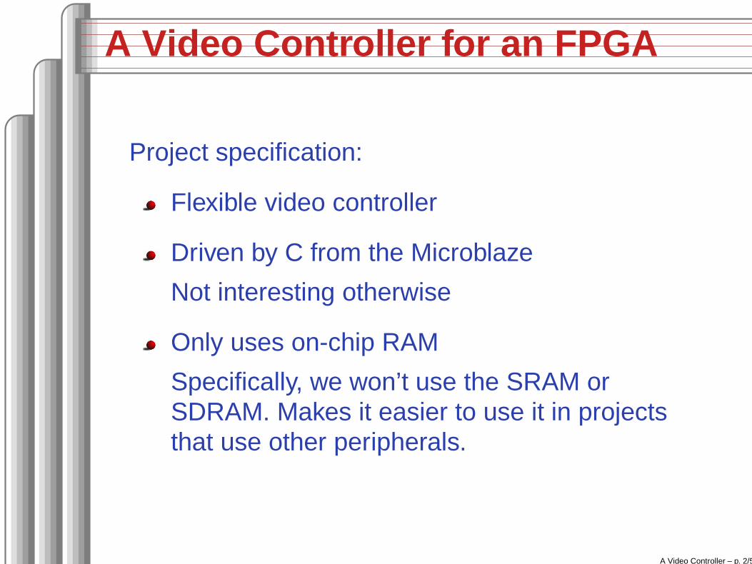
A Video Controller for an FPGA
Project specification:
Flexible video controller
Driven by C from the Microblaze
Not interesting otherwise
Only uses on-chip RAM
Specifically, we won’t use the SRAM orSDRAM. Makes it easier to use it in projectsthat use other peripherals.
A Video Controller – p. 2/57
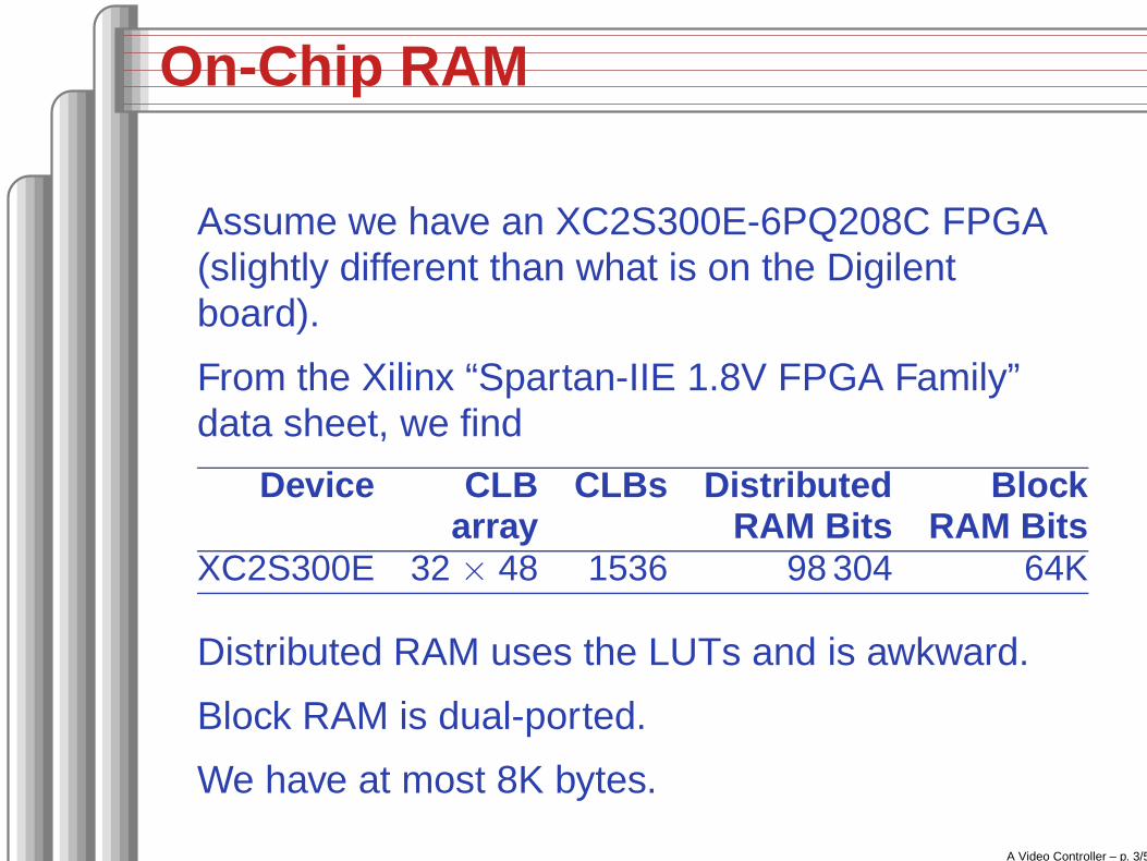
On-Chip RAM
Assume we have an XC2S300E-6PQ208C FPGA(slightly different than what is on the Digilentboard).
From the Xilinx “Spartan-IIE 1.8V FPGA Family”data sheet, we find
Device CLB CLBs Distributed Blockarray RAM Bits RAM Bits
XC2S300E 32 × 48 1536 98 304 64K
Distributed RAM uses the LUTs and is awkward.
Block RAM is dual-ported.
We have at most 8K bytes.
A Video Controller – p. 3/57
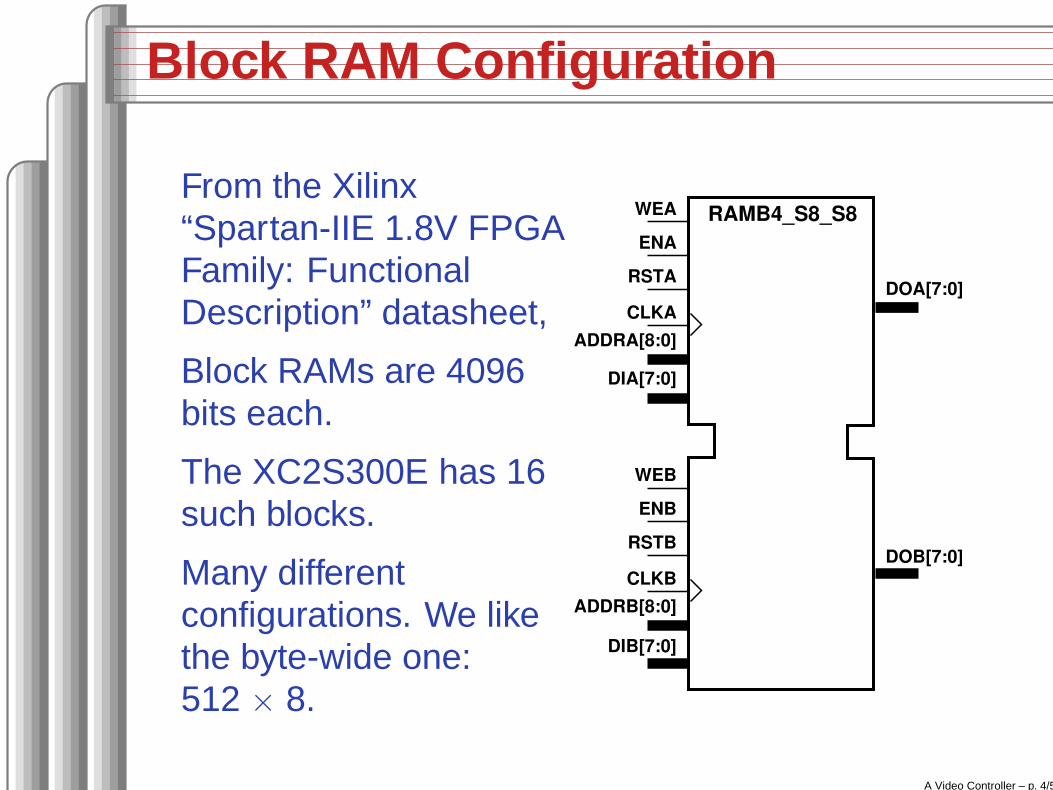
Block RAM Configuration
From the Xilinx“Spartan-IIE 1.8V FPGAFamily: FunctionalDescription” datasheet,
Block RAMs are 4096bits each.
The XC2S300E has 16such blocks.
Many differentconfigurations. We likethe byte-wide one:512 × 8.
A Video Controller – p. 4/57
Dual-Ported RAM
The dual-ported nature is very convenient.
Two truly independent input/output ports that donot have to be synchronized.
We will use one port for the video controller, theother for the processor.
A Video Controller – p. 5/57
Memory Usage
VGA is 640 × 480 = 307 200 pixels
Even at one bit per pixel, this requires307 200 ÷ 1024 = 300K bits = 37.5K bytes
Too much for on-chip RAM; we only have 8K max.
A Video Controller – p. 6/57
Memory Usage
How about a text-only display?
80 × 24 is typical.
640 ÷ 80 = 8 pixels horizontally/character
480 ÷ 24 = 20 pixels vertically/character
A bit too vertical. 8 × 16 is more typical.
480 ÷ 16 = 30 lines
80 × 30 = 2400 characters
Over 2K (2048). 2400 = 2048 + 352
Will fit in 2.5K = 2560
A Video Controller – p. 7/57
Font
How about the font?
For 8 × 16 characters, the 96 basic ASCIIcharacters take
16 × 96 = 1536 = 1.5K
A Video Controller – p. 8/57
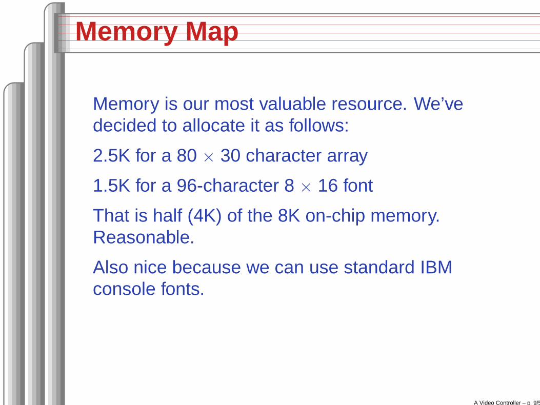
Memory Map
Memory is our most valuable resource. We’vedecided to allocate it as follows:
2.5K for a 80 × 30 character array
1.5K for a 96-character 8 × 16 font
That is half (4K) of the 8K on-chip memory.Reasonable.
Also nice because we can use standard IBMconsole fonts.
A Video Controller – p. 9/57
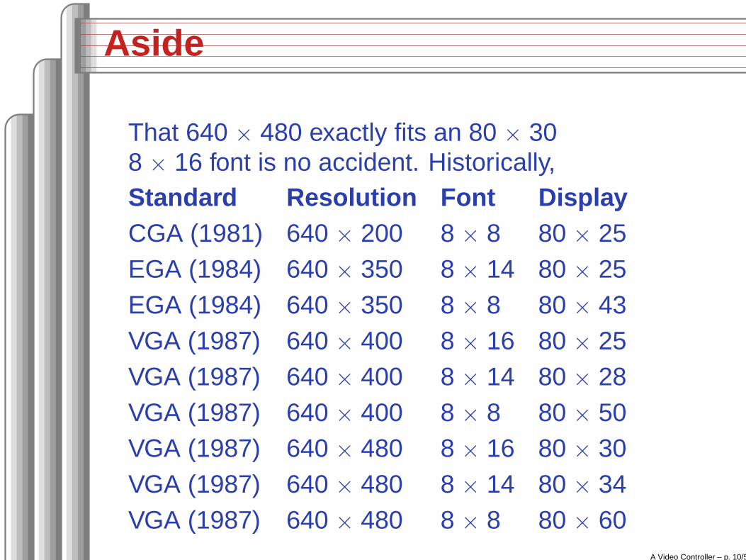
Aside
That 640 × 480 exactly fits an 80 × 308 × 16 font is no accident. Historically,Standard Resolution Font DisplayCGA (1981) 640 × 200 8 × 8 80 × 25EGA (1984) 640 × 350 8 × 14 80 × 25EGA (1984) 640 × 350 8 × 8 80 × 43VGA (1987) 640 × 400 8 × 16 80 × 25VGA (1987) 640 × 400 8 × 14 80 × 28VGA (1987) 640 × 400 8 × 8 80 × 50VGA (1987) 640 × 480 8 × 16 80 × 30VGA (1987) 640 × 480 8 × 14 80 × 34VGA (1987) 640 × 480 8 × 8 80 × 60
A Video Controller – p. 10/57
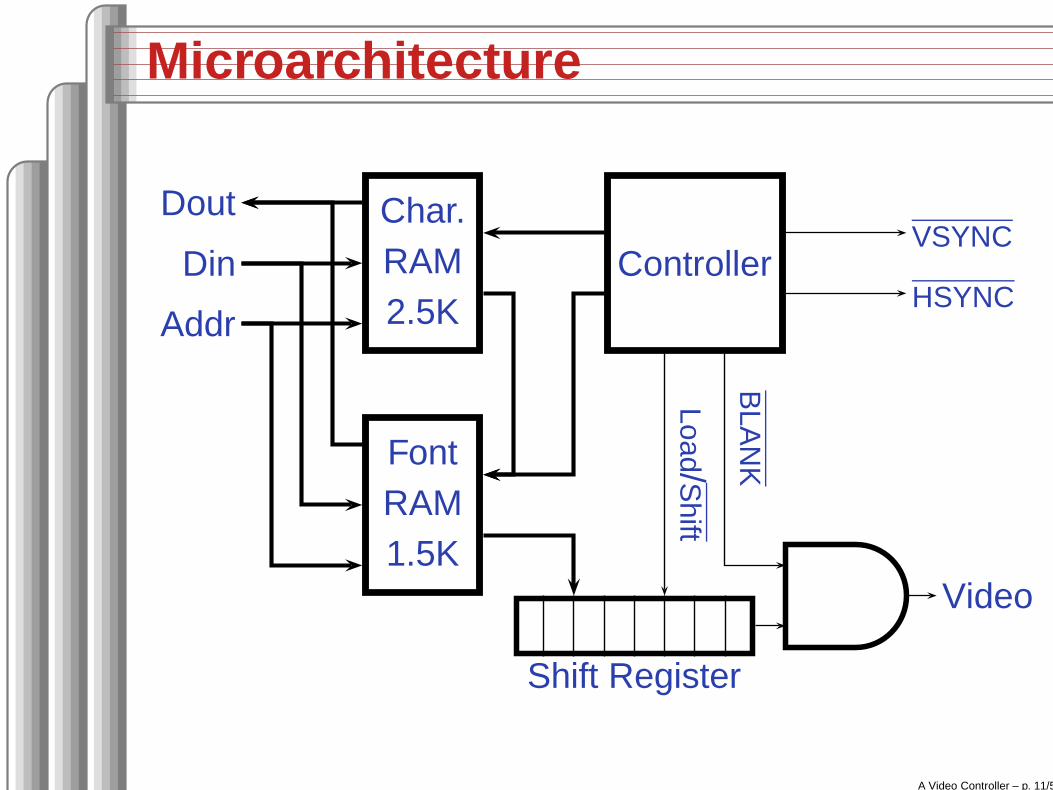
Microarchitecture
Char.RAM2.5K
FontRAM1.5K
Controller
Shift Register
Dout
Din
Addr
VSYNC
HSYNC
Video
BLA
NK
Load/Shift
A Video Controller – p. 11/57
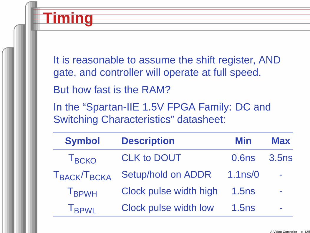
Timing
It is reasonable to assume the shift register, ANDgate, and controller will operate at full speed.
But how fast is the RAM?
In the “Spartan-IIE 1.5V FPGA Family: DC andSwitching Characteristics” datasheet:
Symbol Description Min Max
TBCKO CLK to DOUT 0.6ns 3.5ns
TBACK/TBCKA Setup/hold on ADDR 1.1ns/0 -
TBPWH Clock pulse width high 1.5ns -
TBPWL Clock pulse width low 1.5ns -
A Video Controller – p. 12/57
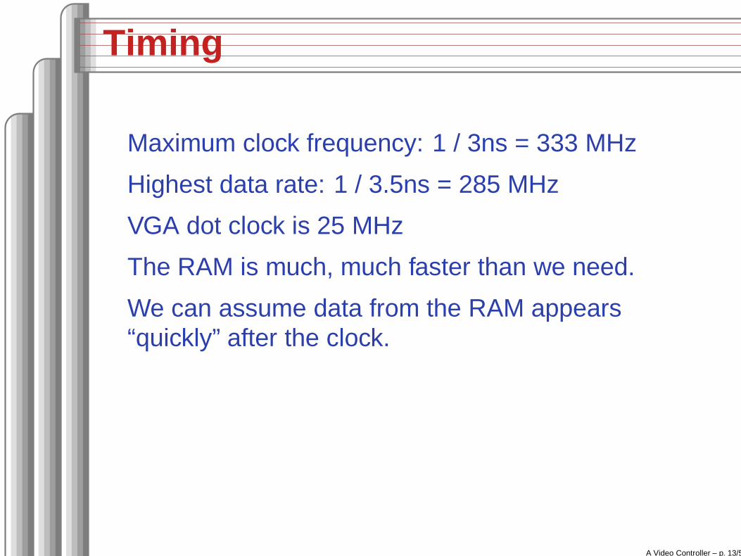
Timing
Maximum clock frequency: 1 / 3ns = 333 MHz
Highest data rate: 1 / 3.5ns = 285 MHz
VGA dot clock is 25 MHz
The RAM is much, much faster than we need.
We can assume data from the RAM appears“quickly” after the clock.
A Video Controller – p. 13/57
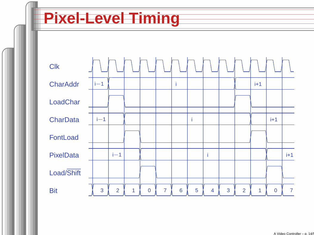
Pixel-Level Timing
Clk
CharAddr
� � � � � � � � � � � � � � � � � � � � � � � � � � � � � � � � � � � � � � � � � � � � � � � �
i−1 i i+1
LoadChar
� � � �
� �
� � � � � � � � � � � � � � � � � � � � � � � � � �
� �
� � � � � � � � � �
CharData
� � � � � � � � � � � � � � � � � � � � � � � � � � � � � � � � � � � � � � � � � � � � � � � �
i−1 i i+1
FontLoad
� � � � � � � �
� �
� � � � � � � � � � � � � � � � � � � � � � � � � �
� �
� � � � � �
PixelData
� � � � � � � � � � � � � � � � � � � � � � � � � � � � � � � � � � � � � � � � � � � � � � � �
i−1 i i+1
Load/Shift
� � � � � � � � � � � �
� �
� � � � � � � � � � � � � � � � � � � � � � � � � �
� �
� �
Bit
� � � � � � � � � � � � � � � � � � � � � � � � � �
3 2 1 0 7 6 5 4 3 2 1 0 7
A Video Controller – p. 14/57
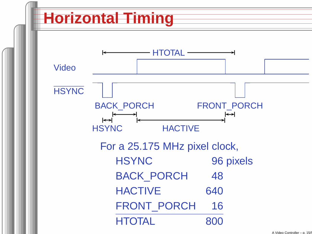
Horizontal Timing
Video
� � � � � � � � � � � � � �
HSYNC
� � � � � � � � � � � � � � � � � � � � � � � � � � � � � � � � � � � �
HTOTAL
HSYNC
BACK_PORCH
HACTIVE
FRONT_PORCH
For a 25.175 MHz pixel clock,HSYNC 96 pixelsBACK_PORCH 48HACTIVE 640FRONT_PORCH 16
HTOTAL 800A Video Controller – p. 15/57
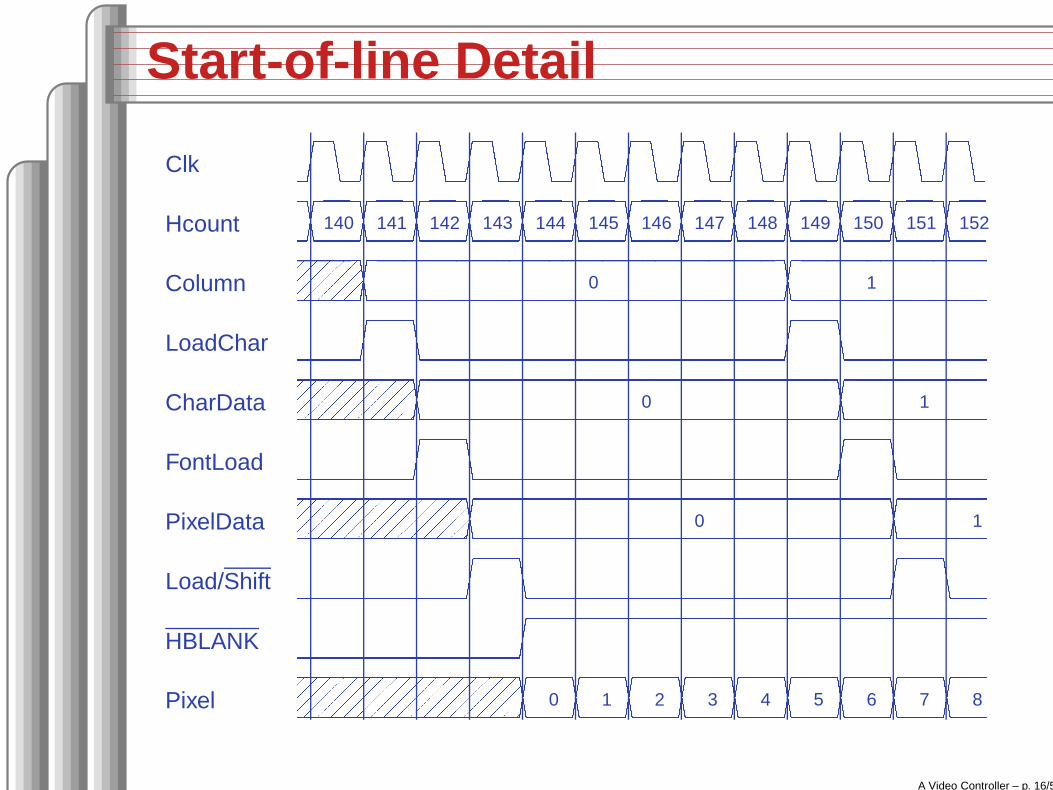
Start-of-line Detail
140 141 142 143 144 145 146 147 148 149 150 151 152
Clk
Hcount
� � � � � � � � � � � � � � � � � � � � � � � � � �
Column
� � � � � � � � � � � � � � � � � � � � � � � � � � � � � � � � � � � � � � � � � � � � � � � �
0 1
LoadChar
� � � �
� �
� � � � � � � � � � � � � � � � � � � � � � � � � �
� �
� � � � � � � � � �
CharData
� � � � � � � � � � � � � � � � � � � � � � � � � � � � � � � � � � � � � � � � � � � � � � � �
0 1
FontLoad
� � � � � � � �
� �
� � � � � � � � � � � � � � � � � � � � � � � � � �
� �
� � � � � �
PixelData
� � � � � � � � � � � � � � � � � � � � � � � � � � � � � � � � � � � � � � � � � � � � � � � �
0 1
Load/Shift
� � � � � � � � � � � �
� �
� � � � � � � � � � � � � � � � � � � � � � � � � �
� �
� �
HBLANK
� � � � � � � � � � � � � � � �
� � � � � � � � � � � � � � � � � � � � � � � � � � � � � � � � � �
Pixel
� � � � � � � � � � � � � � � � � � � � � � � � � � � � � � � � � �
0 1 2 3 4 5 6 7 8
A Video Controller – p. 16/57
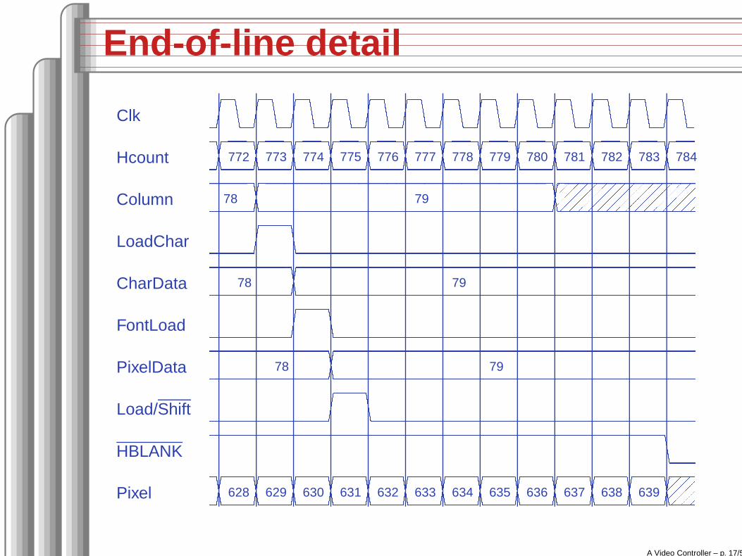
End-of-line detail
772 773 774 775 776 777 778 779 780 781 782 783 784
Clk
Hcount
� � � � � � � � � � � � � � � � � � � � � � � � � �
Column
� � � � � � � � � � � � � � � � � � � � � � � � � � � � � � � � � � � � � � � � � � � � � � � �
78 79
LoadChar
� � � �
� �
� � � � � � � � � � � � � � � � � � � � � � � � � � � � � � � � � � � � � � � � � �
CharData
� � � � � � � � � � � � � � � � � � � � � � � � � � � � � � � � � � � � � � � � � � � � � � � � � �
78 79
FontLoad
� � � � � � � �
� �
� � � � � � � � � � � � � � � � � � � � � � � � � � � � � � � � � � � � � �
PixelData
� � � � � � � � � � � � � � � � � � � � � � � � � � � � � � � � � � � � � � � � � � � � � � � � � �
78 79
Load/Shift
� � � � � � � � � � � �
� �
� � � � � � � � � � � � � � � � � � � � � � � � � � � � � � � � � �
HBLANK
� � � � � � � � � � � � � � � � � � � � � � � � � � � � � � � � � � � � � � � � � � � � � � � �
� �
Pixel� � � � � � � � � � � � � � � � � � � � � � � � � �
628 629 630 631 632 633 634 635 636 637 638 639
A Video Controller – p. 17/57
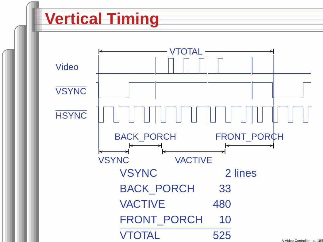
Vertical Timing
Video
VSYNC
HSYNC
� � � � � � � � � � � � � � � � � � � � � � ��
� � � � � � � �
�� � � � � � � � � � � � �
�� � � � � � � � � � � � � � � � � � � � � � �
� � � � � � � � � �
� � � � � � � � � � � � � � � � � � � � � � � � � � � � � � � � � � � � � � � � � � � � � � � � � � � � � � � �
� � � � � � � � � �
� �
� � � � � � � � � � � � � � � � � � � � � � � � � � � � � �
VTOTAL
VSYNC
BACK_PORCH
VACTIVE
FRONT_PORCH
VSYNC 2 linesBACK_PORCH 33VACTIVE 480FRONT_PORCH 10VTOTAL 525
A Video Controller – p. 18/57
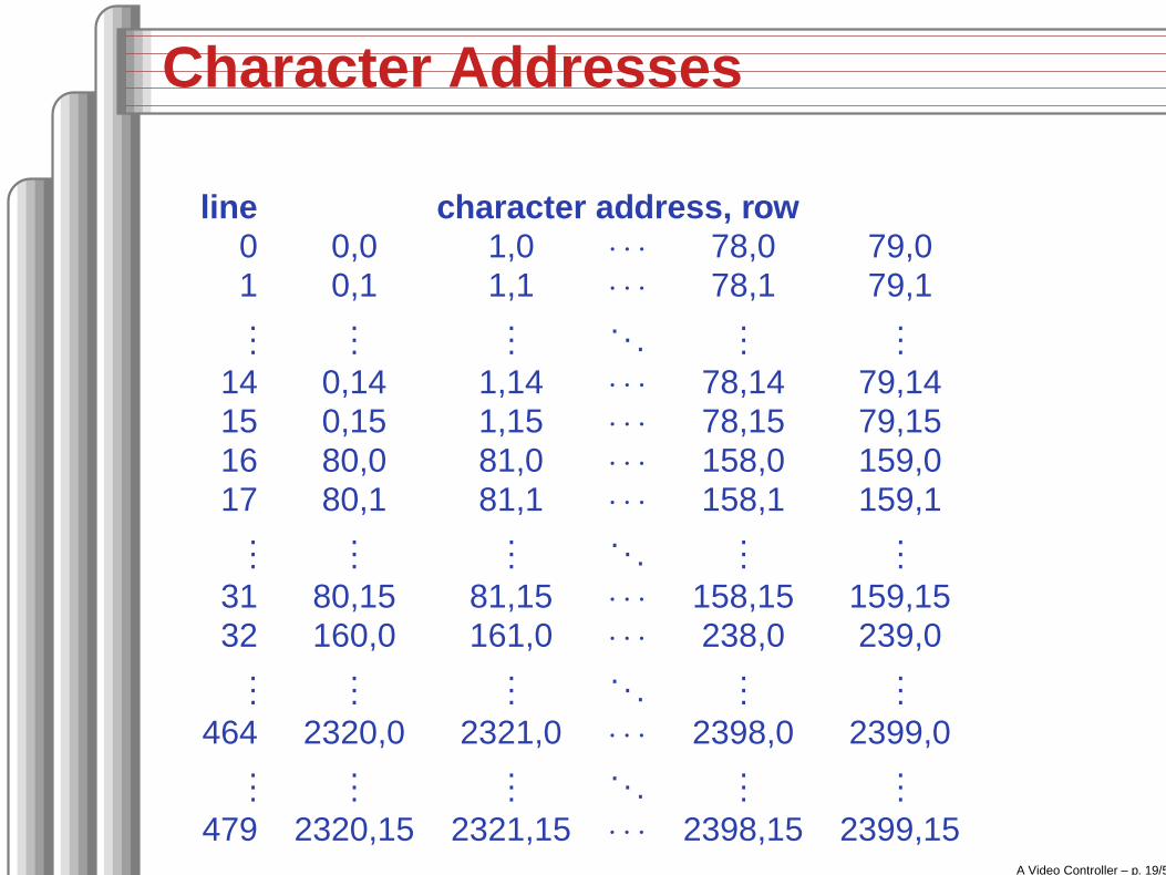
Character Addresses
line character address, row0 0,0 1,0 · · · 78,0 79,01 0,1 1,1 · · · 78,1 79,1...
......
. . ....
...14 0,14 1,14 · · · 78,14 79,1415 0,15 1,15 · · · 78,15 79,1516 80,0 81,0 · · · 158,0 159,017 80,1 81,1 · · · 158,1 159,1
......
.... . .
......
31 80,15 81,15 · · · 158,15 159,1532 160,0 161,0 · · · 238,0 239,0
......
.... . .
......
464 2320,0 2321,0 · · · 2398,0 2399,0...
......
. . ....
...479 2320,15 2321,15 · · · 2398,15 2399,15
A Video Controller – p. 19/57
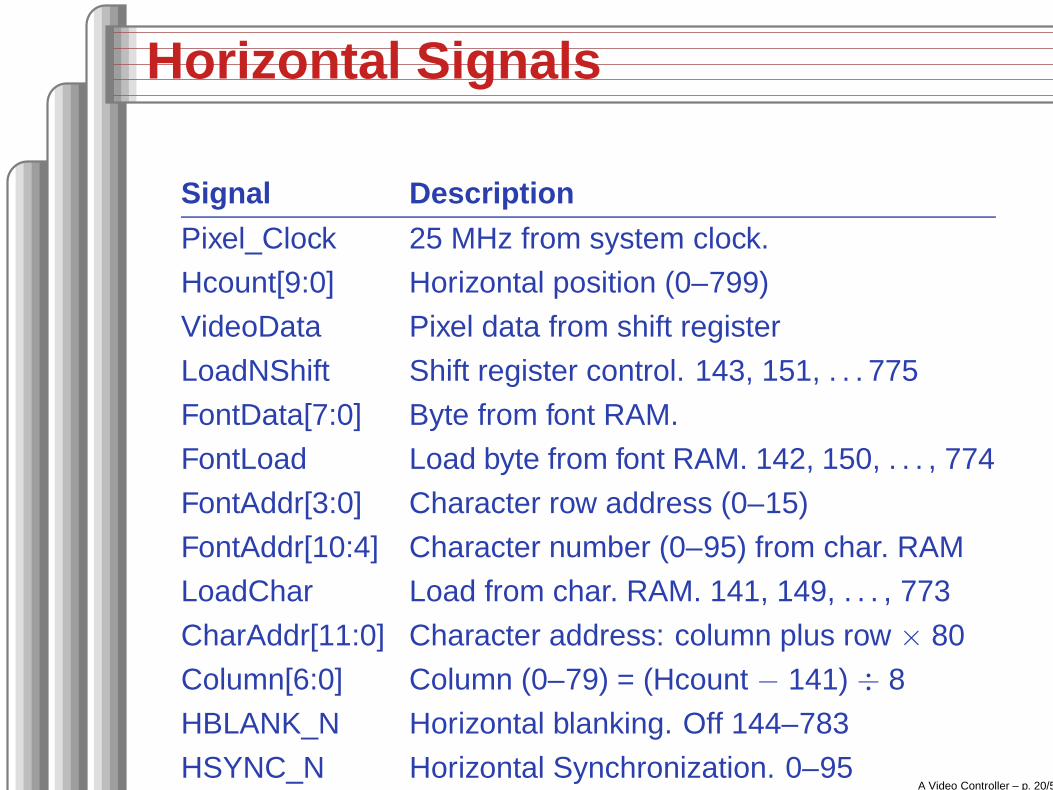
Horizontal Signals
Signal Description
Pixel_Clock 25 MHz from system clock.
Hcount[9:0] Horizontal position (0–799)
VideoData Pixel data from shift register
LoadNShift Shift register control. 143, 151, . . . 775
FontData[7:0] Byte from font RAM.
FontLoad Load byte from font RAM. 142, 150, . . . , 774
FontAddr[3:0] Character row address (0–15)
FontAddr[10:4] Character number (0–95) from char. RAM
LoadChar Load from char. RAM. 141, 149, . . . , 773
CharAddr[11:0] Character address: column plus row × 80
Column[6:0] Column (0–79) = (Hcount − 141) ÷ 8
HBLANK_N Horizontal blanking. Off 144–783
HSYNC_N Horizontal Synchronization. 0–95A Video Controller – p. 20/57
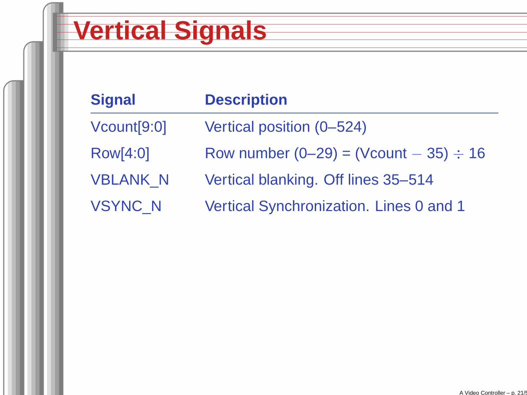
Vertical Signals
Signal Description
Vcount[9:0] Vertical position (0–524)
Row[4:0] Row number (0–29) = (Vcount − 35) ÷ 16
VBLANK_N Vertical blanking. Off lines 35–514
VSYNC_N Vertical Synchronization. Lines 0 and 1
A Video Controller – p. 21/57
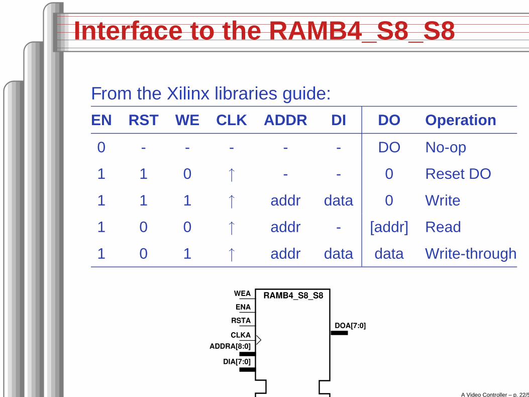
Interface to the RAMB4_S8_S8
From the Xilinx libraries guide:EN RST WE CLK ADDR DI DO Operation
0 - - - - - DO No-op
1 1 0 ↑ - - 0 Reset DO
1 1 1 ↑ addr data 0 Write
1 0 0 ↑ addr - [addr] Read
1 0 1 ↑ addr data data Write-through
A Video Controller – p. 22/57
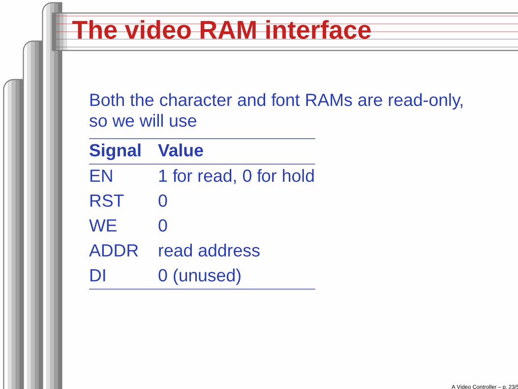
The video RAM interface
Both the character and font RAMs are read-only,so we will use
Signal ValueEN 1 for read, 0 for holdRST 0WE 0ADDR read addressDI 0 (unused)
A Video Controller – p. 23/57
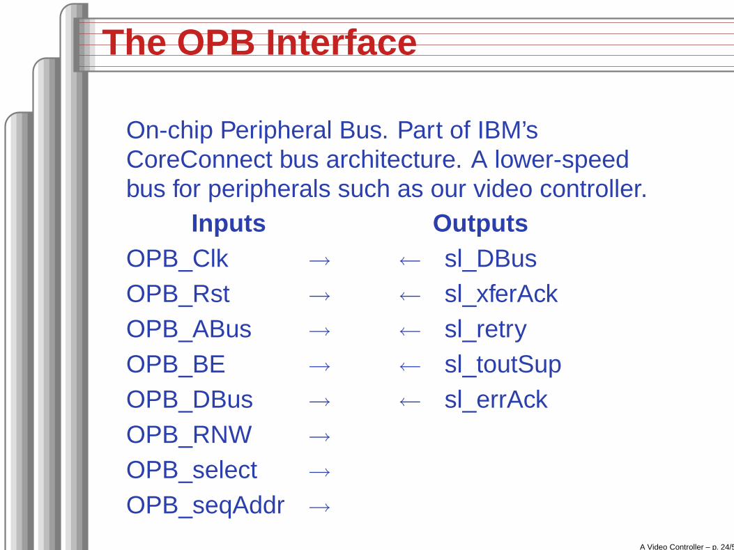
The OPB Interface
On-chip Peripheral Bus. Part of IBM’sCoreConnect bus architecture. A lower-speedbus for peripherals such as our video controller.
InputsOPB_Clk →
OPB_Rst →
OPB_ABus →
OPB_BE →
OPB_DBus →
OPB_RNW →
OPB_select →
OPB_seqAddr →
Outputs← sl_DBus← sl_xferAck← sl_retry← sl_toutSup← sl_errAck
A Video Controller – p. 24/57
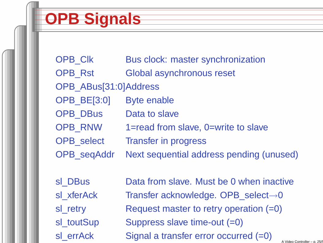
OPB Signals
OPB_Clk Bus clock: master synchronization
OPB_Rst Global asynchronous reset
OPB_ABus[31:0]Address
OPB_BE[3:0] Byte enable
OPB_DBus Data to slave
OPB_RNW 1=read from slave, 0=write to slave
OPB_select Transfer in progress
OPB_seqAddr Next sequential address pending (unused)
sl_DBus Data from slave. Must be 0 when inactive
sl_xferAck Transfer acknowledge. OPB_select→0
sl_retry Request master to retry operation (=0)
sl_toutSup Suppress slave time-out (=0)
sl_errAck Signal a transfer error occurred (=0)A Video Controller – p. 25/57
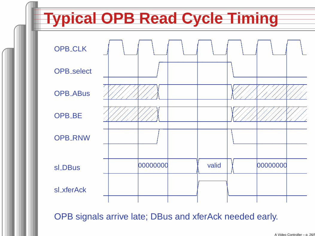
Typical OPB Read Cycle Timing
OPB CLK
�
�
�
�
�
�
�
�
�
�
�
�
�
OPB select
� � � � � � � � � �
� � � � � � � � � � � � �
� � � � � � � � � � � � � �
OPB ABus
OPB BE
OPB RNW� � � � � � � � � � � � �
sl DBus 00000000 valid 00000000
sl xferAck
� � � � � � � � � � � � � � � � � �
� � � �
� � � � � � � � � � � � � � �
OPB signals arrive late; DBus and xferAck needed early.
A Video Controller – p. 26/57
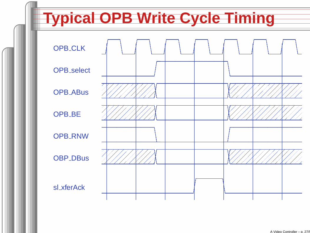
Typical OPB Write Cycle Timing
OPB CLK
�
�
�
�
�
�
�
�
�
�
�
�
�
OPB select
� � � � � � � � � �
� � � � � � � � � � � � �
� � � � � � � � � � � � � �
OPB ABus
OPB BE
OPB RNW� � � � � � � � � � � � �
OBP DBus
sl xferAck
� � � � � � � � � � � � � � � � � �
� � � �
� � � � � � � � � � � � � � �
A Video Controller – p. 27/57
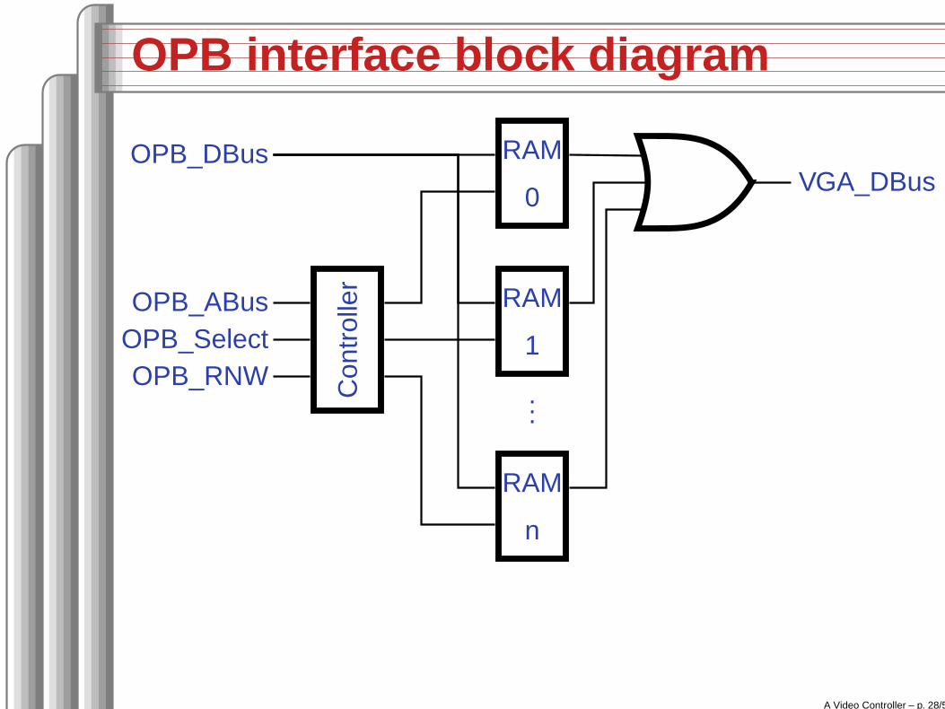
OPB interface block diagram
RAM
n
RAM
1
RAM
0
...
OPB_DBusVGA_DBus
Con
trol
ler
OPB_ABusOPB_SelectOPB_RNW
A Video Controller – p. 28/57
OPB-RAM Read Timing
OPB CLK
�
�
�
�
�
�
�
�
�
�
�
�
�
OPB select
� � � � � � � � � �
� � � � � � � � � � � � � � � � � � �
� � � � � � � �
OPB ABus
� � � � � � � � � � � � � � � � � � � � � � � � � � � � � � � � � � � � �
OPB RNW
� � � � � � � � � � � � � � � � � � � � � � � � � � � � � � � � � � � � �
RAM-Data
� � � � � � � � � � � � � � � � � � � � � � � � � � � � � � � � � � � � �
VGA DBus
� � � � � � � � � � � � � � � � � � � � � � � � � � � � � � � � � � � � �
00000000 valid 00000000
RST
� � � � � � � � � � � � � � � � � � � � � � � � � � � � � � � � � � � � �
(one only)
WE
� � � � � � � � � � � � � � � � � � � � � � � � � � � � � � � � � � � � � � � � �
(always low)
MemCycle1
� � � � � � � � � � � � � � � � � �
� � � �
� � � � � � � � � � � � � � �
MemCycle2� � � � � � � � � � � � � � � � � � � � � � � �
� � � �
� � � � � � � � �
VGA xferAck
� � � � � � � � � � � � � � � � � � � � � � � �
� � � �
� � � � � � � � �
A Video Controller – p. 29/57
OPB-RAM Write Timing
OPB CLK
�
�
�
�
�
�
�
�
�
�
�
�
� �
OPB select
� � � � � � � � � �
� � � � � � � � � � � � � � � � � � �
� � � � � � �
OPB ABus
OPB RNW
� � � � � � � � � � � � � � � � � � �
OPB DBus
RST
� � � � � � � � � � � � � � � � � � � � � � � � � � � � � � � � � � � � � � � �
(always high)
WE
� � � � � � � � � � � � � � � � � � � � � � � � � � � � � � � �
(one only)
MemCycle1� � � � � � � � � � � � � � � � � �
� � � �
� � � � � � � � � � � � � �
MemCycle2
� � � � � � � � � � � � � � � � � � � � � � � �
� � � �
� � � � � � � �
VGA xferAck
� � � � � � � � � � � � � � � � � � � � � � � �
� � � �
� � � � � � � �A Video Controller – p. 30/57
VHDL: Entity generics
library ieee;use ieee.std_logic_1164.all;use ieee.std_logic_arith.all;use ieee.std_logic_unsigned.all;
entity opb_xsb300e_vga isgeneric (
C_OPB_AWIDTH : integer := 32;C_OPB_DWIDTH : integer := 32;C_BASEADDR : std_logic_vector(31 downto 0)
:= X"FEFF1000";C_HIGHADDR : std_logic_vector(31 downto 0)
:= X"FEFF1FFF");
A Video Controller – p. 31/57
VHDL: OPB Ports
port (OPB_Clk : in std_logic;OPB_Rst : in std_logic;
-- OPB signalsOPB_ABus : in std_logic_vector(31 downto 0);OPB_BE : in std_logic_vector(3 downto 0);OPB_DBus : in std_logic_vector(31 downto 0);OPB_RNW : in std_logic;OPB_select : in std_logic;OPB_seqAddr : in std_logic;
VGA_DBus : out std_logic_vector(31 downto 0);VGA_errAck : out std_logic;VGA_retry : out std_logic;VGA_toutSup : out std_logic;VGA_xferAck : out std_logic;
A Video Controller – p. 32/57
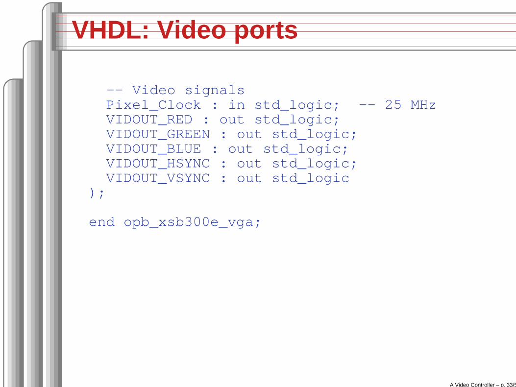
VHDL: Video ports
-- Video signalsPixel_Clock : in std_logic; -- 25 MHzVIDOUT_RED : out std_logic;VIDOUT_GREEN : out std_logic;VIDOUT_BLUE : out std_logic;VIDOUT_HSYNC : out std_logic;VIDOUT_VSYNC : out std_logic
);
end opb_xsb300e_vga;
A Video Controller – p. 33/57
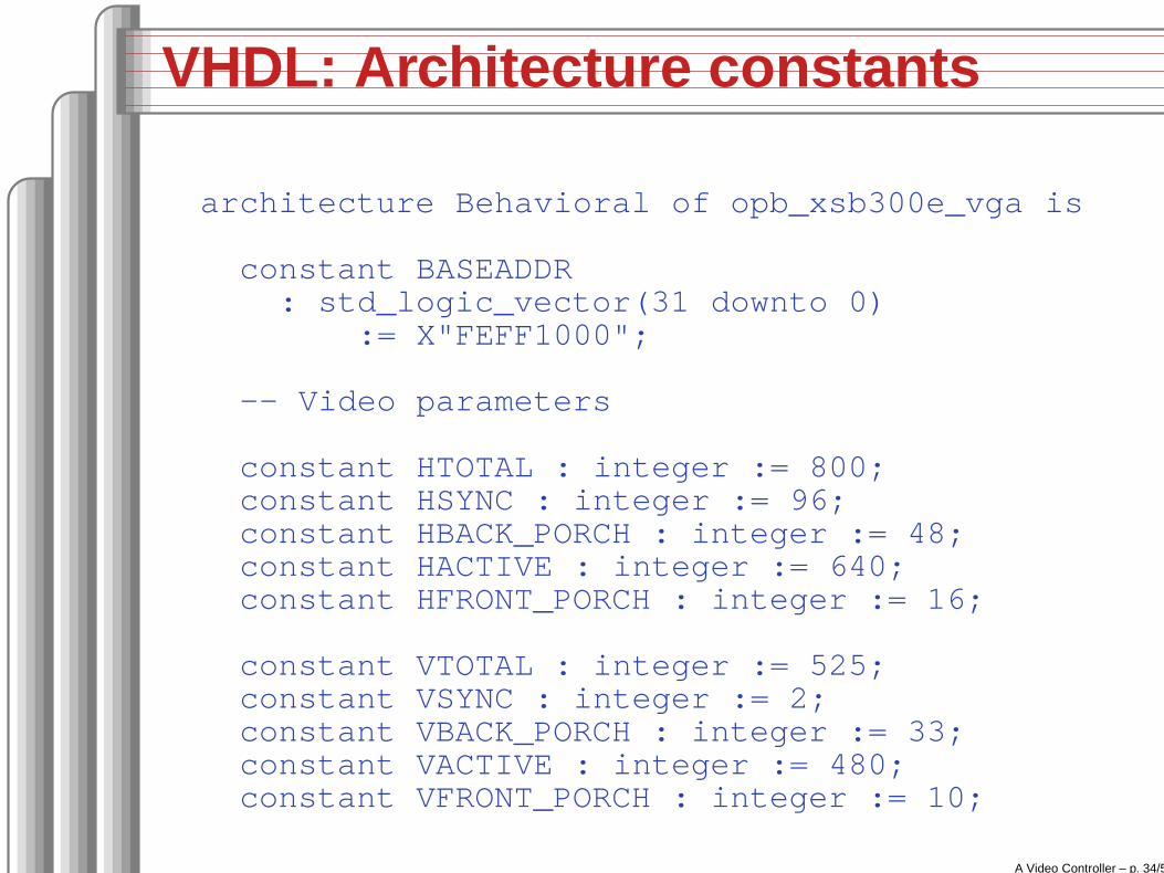
VHDL: Architecture constants
architecture Behavioral of opb_xsb300e_vga is
constant BASEADDR: std_logic_vector(31 downto 0)
:= X"FEFF1000";
-- Video parameters
constant HTOTAL : integer := 800;constant HSYNC : integer := 96;constant HBACK_PORCH : integer := 48;constant HACTIVE : integer := 640;constant HFRONT_PORCH : integer := 16;
constant VTOTAL : integer := 525;constant VSYNC : integer := 2;constant VBACK_PORCH : integer := 33;constant VACTIVE : integer := 480;constant VFRONT_PORCH : integer := 10;
A Video Controller – p. 34/57
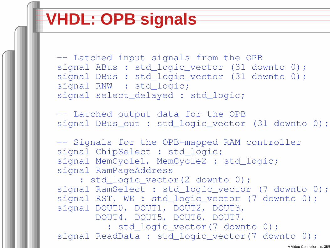
VHDL: OPB signals
-- Latched input signals from the OPBsignal ABus : std_logic_vector (31 downto 0);signal DBus : std_logic_vector (31 downto 0);signal RNW : std_logic;signal select_delayed : std_logic;
-- Latched output data for the OPBsignal DBus_out : std_logic_vector (31 downto 0);
-- Signals for the OPB-mapped RAM controllersignal ChipSelect : std_logic;signal MemCycle1, MemCycle2 : std_logic;signal RamPageAddress
: std_logic_vector(2 downto 0);signal RamSelect : std_logic_vector (7 downto 0);signal RST, WE : std_logic_vector (7 downto 0);signal DOUT0, DOUT1, DOUT2, DOUT3,
DOUT4, DOUT5, DOUT6, DOUT7,: std_logic_vector(7 downto 0);
signal ReadData : std_logic_vector(7 downto 0);A Video Controller – p. 35/57
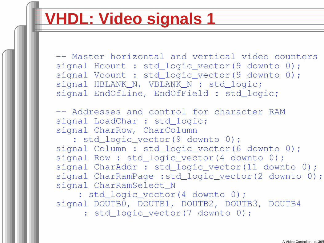
VHDL: Video signals 1
-- Master horizontal and vertical video counterssignal Hcount : std_logic_vector(9 downto 0);signal Vcount : std_logic_vector(9 downto 0);signal HBLANK_N, VBLANK_N : std_logic;signal EndOfLine, EndOfField : std_logic;
-- Addresses and control for character RAMsignal LoadChar : std_logic;signal CharRow, CharColumn
: std_logic_vector(9 downto 0);signal Column : std_logic_vector(6 downto 0);signal Row : std_logic_vector(4 downto 0);signal CharAddr : std_logic_vector(11 downto 0);signal CharRamPage :std_logic_vector(2 downto 0);signal CharRamSelect_N
: std_logic_vector(4 downto 0);signal DOUTB0, DOUTB1, DOUTB2, DOUTB3, DOUTB4
: std_logic_vector(7 downto 0);
A Video Controller – p. 36/57
VHDL: Video signals 2
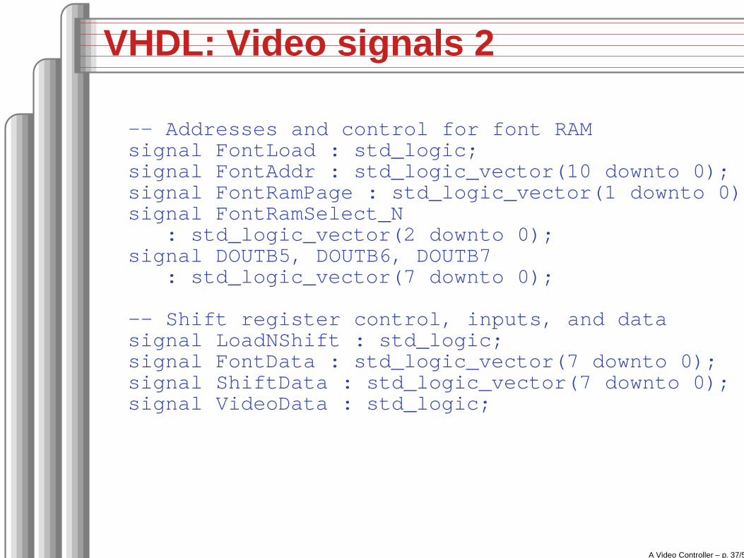
-- Addresses and control for font RAMsignal FontLoad : std_logic;signal FontAddr : std_logic_vector(10 downto 0);signal FontRamPage : std_logic_vector(1 downto 0);signal FontRamSelect_N
: std_logic_vector(2 downto 0);signal DOUTB5, DOUTB6, DOUTB7
: std_logic_vector(7 downto 0);
-- Shift register control, inputs, and datasignal LoadNShift : std_logic;signal FontData : std_logic_vector(7 downto 0);signal ShiftData : std_logic_vector(7 downto 0);signal VideoData : std_logic;
A Video Controller – p. 37/57
VHDL: BRAM component
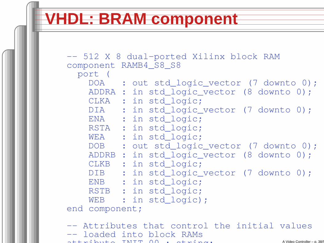
-- 512 X 8 dual-ported Xilinx block RAMcomponent RAMB4_S8_S8
port (DOA : out std_logic_vector (7 downto 0);ADDRA : in std_logic_vector (8 downto 0);CLKA : in std_logic;DIA : in std_logic_vector (7 downto 0);ENA : in std_logic;RSTA : in std_logic;WEA : in std_logic;DOB : out std_logic_vector (7 downto 0);ADDRB : in std_logic_vector (8 downto 0);CLKB : in std_logic;DIB : in std_logic_vector (7 downto 0);ENB : in std_logic;RSTB : in std_logic;WEB : in std_logic);
end component;
-- Attributes that control the initial values-- loaded into block RAMsattribute INIT_00 : string;attribute INIT_01 : string;
A Video Controller – p. 38/57
VHDL: BRAM initialization
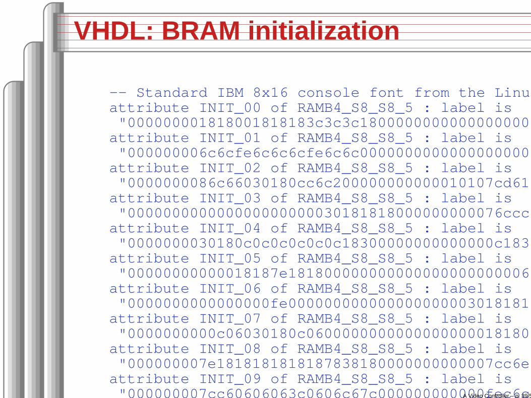
-- Standard IBM 8x16 console font from the Linux file "lat0-16.psfu"attribute INIT_00 of RAMB4_S8_S8_5 : label is"000000001818001818183c3c3c18000000000000000000000000000000000000";
attribute INIT_01 of RAMB4_S8_S8_5 : label is"000000006c6cfe6c6c6cfe6c6c00000000000000000000000000002466666600";
attribute INIT_02 of RAMB4_S8_S8_5 : label is"0000000086c66030180cc6c200000000000010107cd616167cd0d0d67c101000";
attribute INIT_03 of RAMB4_S8_S8_5 : label is"000000000000000000000030181818000000000076ccccccdc76386c6c380000";
attribute INIT_04 of RAMB4_S8_S8_5 : label is"0000000030180c0c0c0c0c0c18300000000000000c18303030303030180c0000";
attribute INIT_05 of RAMB4_S8_S8_5 : label is"00000000000018187e18180000000000000000000000663cff3c660000000000";
attribute INIT_06 of RAMB4_S8_S8_5 : label is"0000000000000000fe0000000000000000000030181818000000000000000000";
attribute INIT_07 of RAMB4_S8_S8_5 : label is"0000000000c06030180c06000000000000000000181800000000000000000000";
attribute INIT_08 of RAMB4_S8_S8_5 : label is"000000007e1818181818187838180000000000007cc6e6e6d6d6cecec67c0000";
attribute INIT_09 of RAMB4_S8_S8_5 : label is"000000007cc60606063c0606c67c000000000000fec6c06030180c06c67c0000";
attribute INIT_0a of RAMB4_S8_S8_5 : label is"000000007cc6060606fcc0c0c0fe0000000000001e0c0c0cfecc6c3c1c0c0000";
A Video Controller – p. 39/57
VHDL: Character BRAM instances
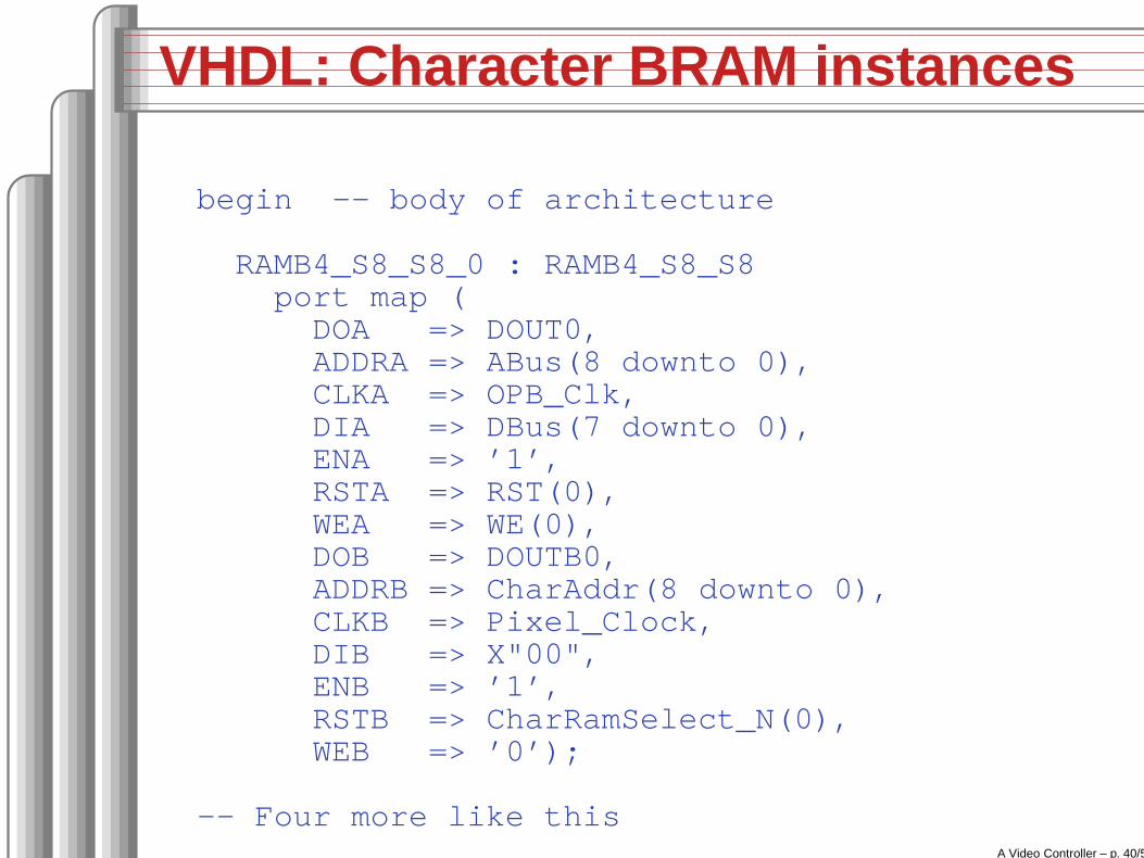
begin -- body of architecture
RAMB4_S8_S8_0 : RAMB4_S8_S8port map (
DOA => DOUT0,ADDRA => ABus(8 downto 0),CLKA => OPB_Clk,DIA => DBus(7 downto 0),ENA => ’1’,RSTA => RST(0),WEA => WE(0),DOB => DOUTB0,ADDRB => CharAddr(8 downto 0),CLKB => Pixel_Clock,DIB => X"00",ENB => ’1’,RSTB => CharRamSelect_N(0),WEB => ’0’);
-- Four more like thisA Video Controller – p. 40/57
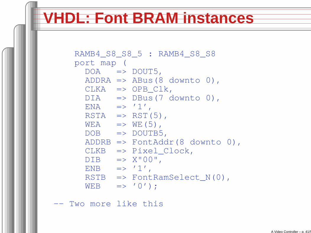
VHDL: Font BRAM instances
RAMB4_S8_S8_5 : RAMB4_S8_S8port map (
DOA => DOUT5,ADDRA => ABus(8 downto 0),CLKA => OPB_Clk,DIA => DBus(7 downto 0),ENA => ’1’,RSTA => RST(5),WEA => WE(5),DOB => DOUTB5,ADDRB => FontAddr(8 downto 0),CLKB => Pixel_Clock,DIB => X"00",ENB => ’1’,RSTB => FontRamSelect_N(0),WEB => ’0’);
-- Two more like this
A Video Controller – p. 41/57
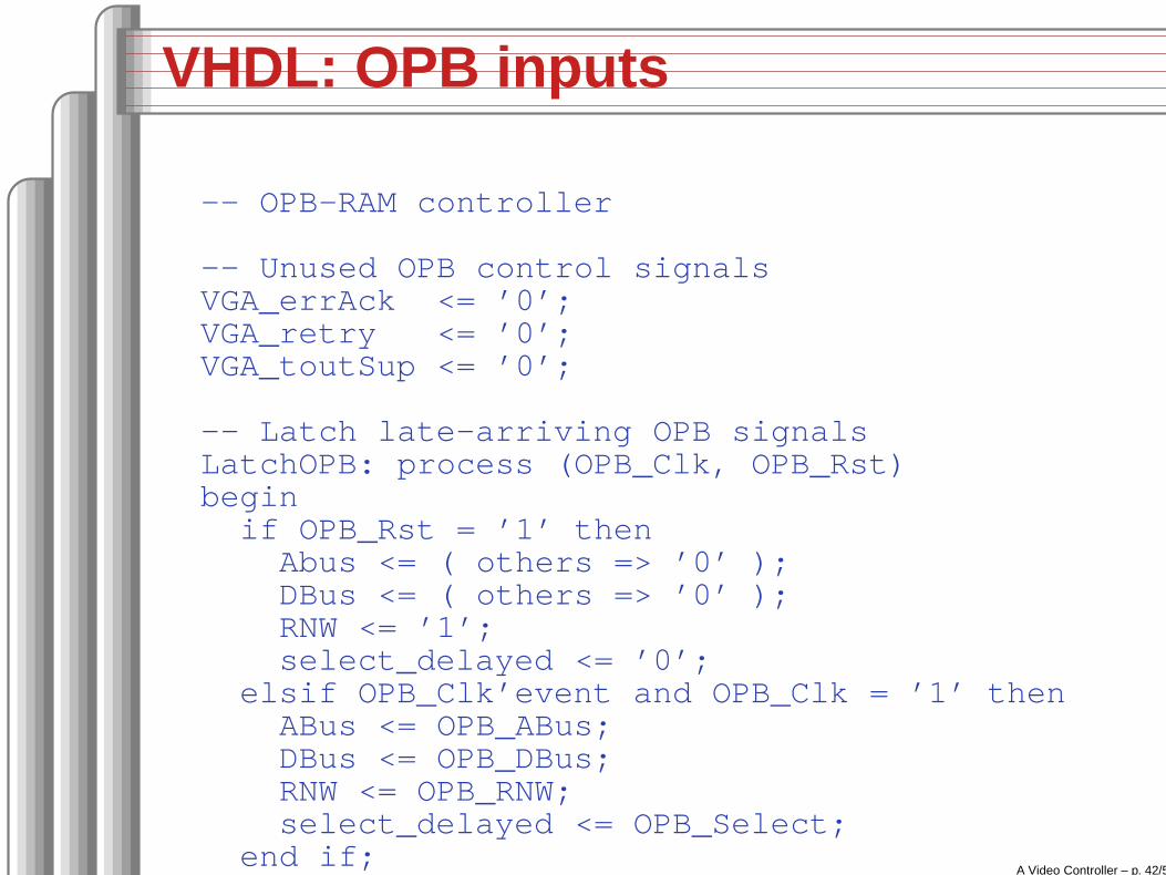
VHDL: OPB inputs
-- OPB-RAM controller
-- Unused OPB control signalsVGA_errAck <= ’0’;VGA_retry <= ’0’;VGA_toutSup <= ’0’;
-- Latch late-arriving OPB signalsLatchOPB: process (OPB_Clk, OPB_Rst)beginif OPB_Rst = ’1’ then
Abus <= ( others => ’0’ );DBus <= ( others => ’0’ );RNW <= ’1’;select_delayed <= ’0’;
elsif OPB_Clk’event and OPB_Clk = ’1’ thenABus <= OPB_ABus;DBus <= OPB_DBus;RNW <= OPB_RNW;select_delayed <= OPB_Select;
end if;end process LatchOPB;
A Video Controller – p. 42/57
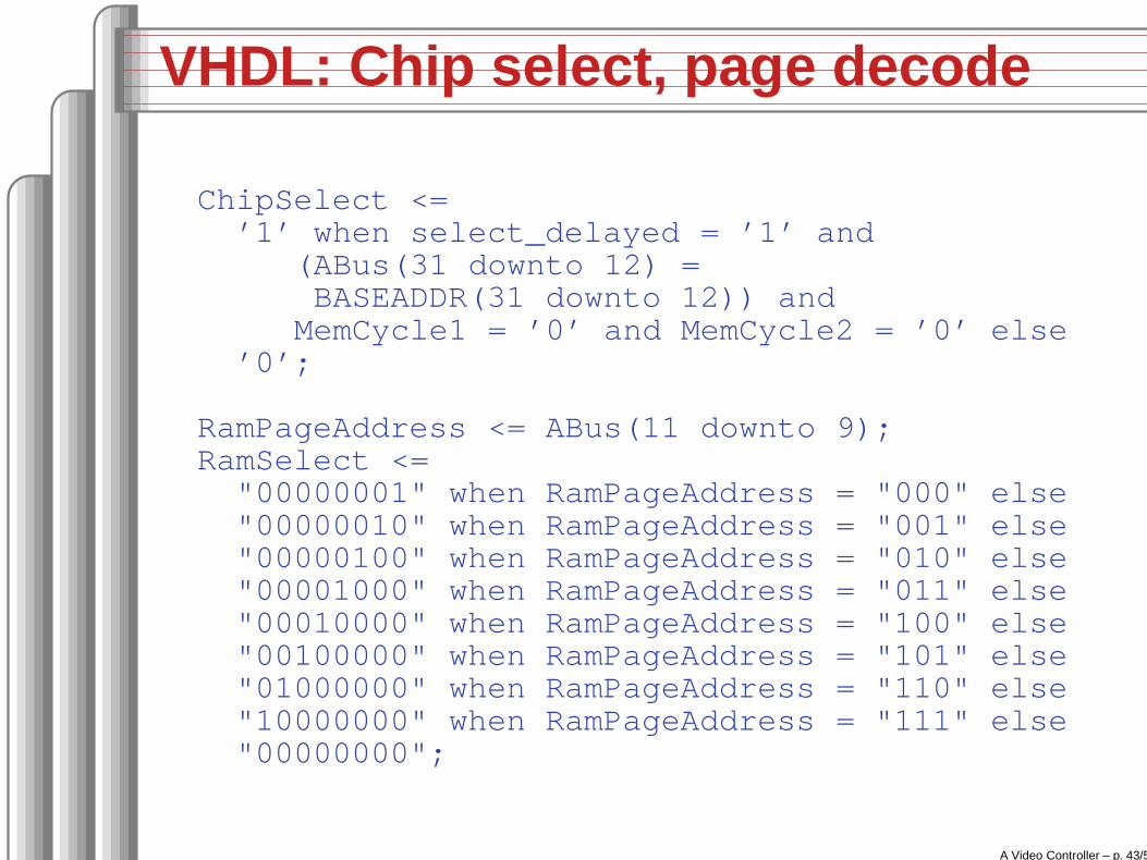
VHDL: Chip select, page decode
ChipSelect <=’1’ when select_delayed = ’1’ and
(ABus(31 downto 12) =BASEADDR(31 downto 12)) andMemCycle1 = ’0’ and MemCycle2 = ’0’ else
’0’;
RamPageAddress <= ABus(11 downto 9);RamSelect <="00000001" when RamPageAddress = "000" else"00000010" when RamPageAddress = "001" else"00000100" when RamPageAddress = "010" else"00001000" when RamPageAddress = "011" else"00010000" when RamPageAddress = "100" else"00100000" when RamPageAddress = "101" else"01000000" when RamPageAddress = "110" else"10000000" when RamPageAddress = "111" else"00000000";
A Video Controller – p. 43/57
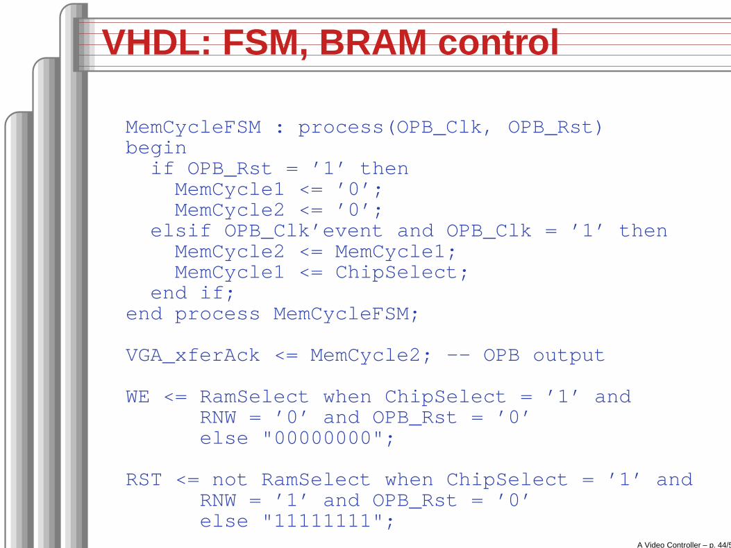
VHDL: FSM, BRAM control
MemCycleFSM : process(OPB_Clk, OPB_Rst)beginif OPB_Rst = ’1’ then
MemCycle1 <= ’0’;MemCycle2 <= ’0’;
elsif OPB_Clk’event and OPB_Clk = ’1’ thenMemCycle2 <= MemCycle1;MemCycle1 <= ChipSelect;
end if;end process MemCycleFSM;
VGA_xferAck <= MemCycle2; -- OPB output
WE <= RamSelect when ChipSelect = ’1’ andRNW = ’0’ and OPB_Rst = ’0’else "00000000";
RST <= not RamSelect when ChipSelect = ’1’ andRNW = ’1’ and OPB_Rst = ’0’else "11111111";
A Video Controller – p. 44/57
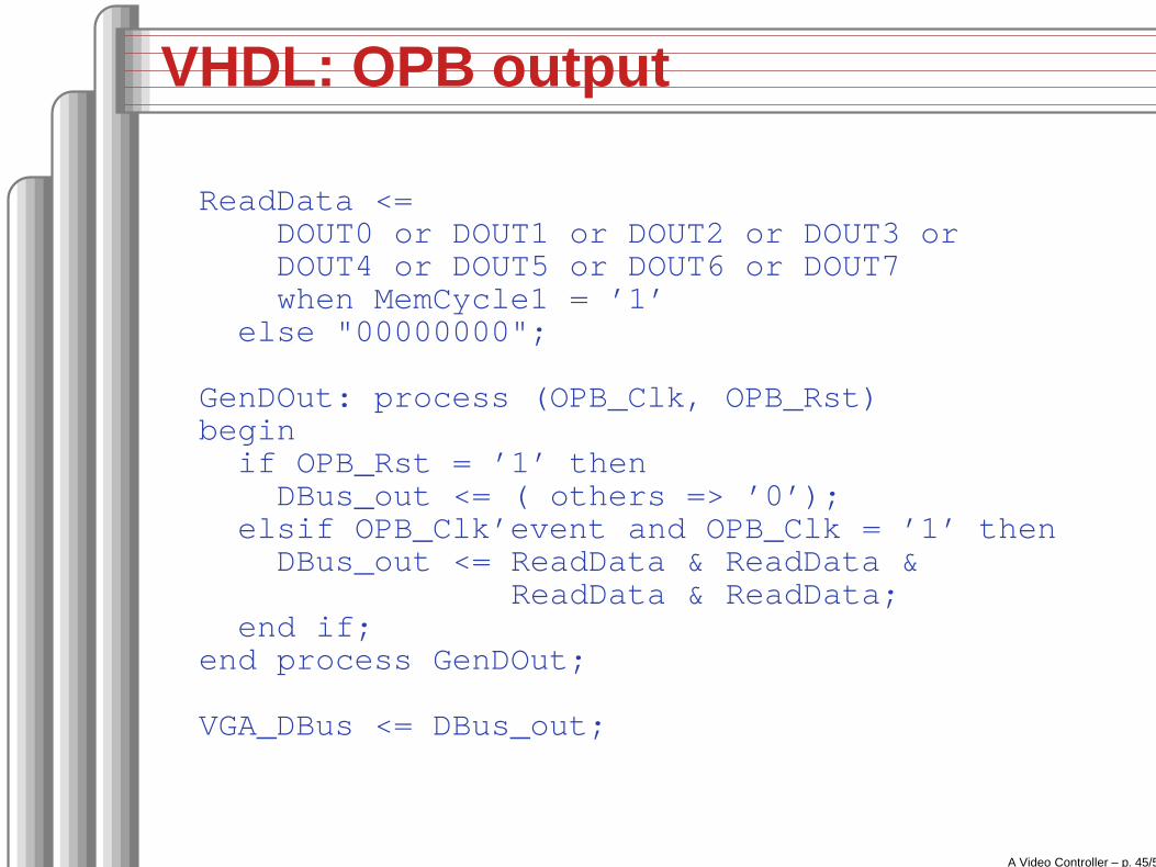
VHDL: OPB output
ReadData <=DOUT0 or DOUT1 or DOUT2 or DOUT3 orDOUT4 or DOUT5 or DOUT6 or DOUT7when MemCycle1 = ’1’
else "00000000";
GenDOut: process (OPB_Clk, OPB_Rst)beginif OPB_Rst = ’1’ then
DBus_out <= ( others => ’0’);elsif OPB_Clk’event and OPB_Clk = ’1’ then
DBus_out <= ReadData & ReadData &ReadData & ReadData;
end if;end process GenDOut;
VGA_DBus <= DBus_out;
A Video Controller – p. 45/57
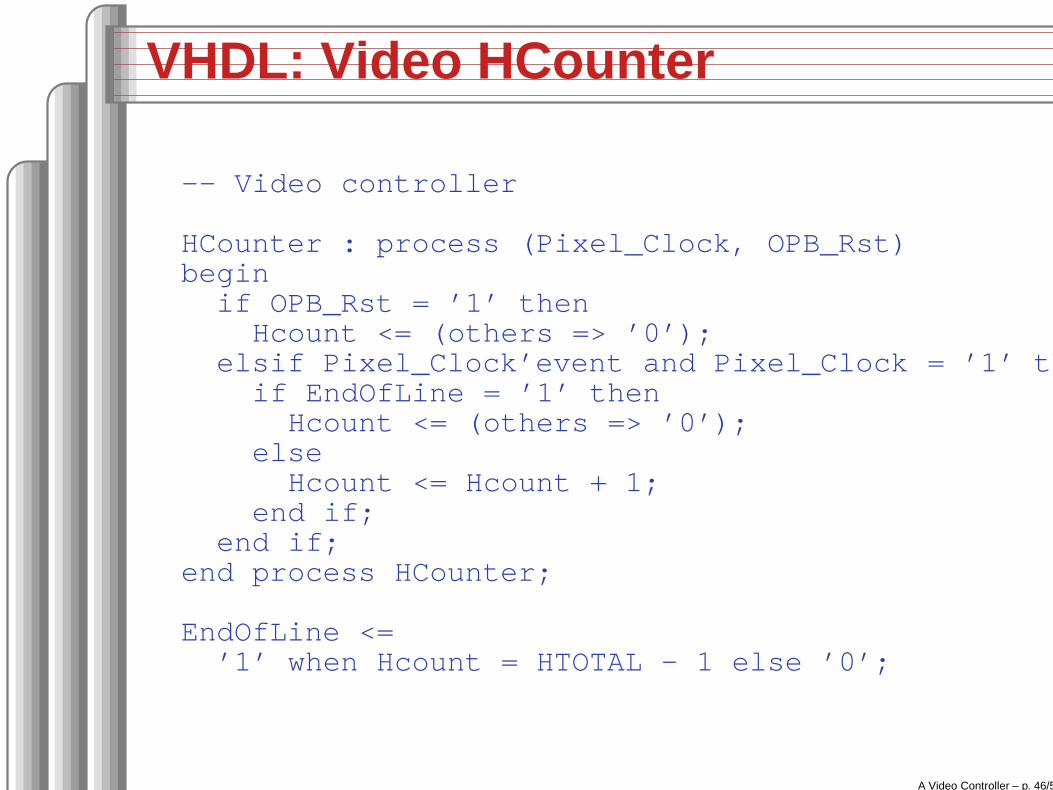
VHDL: Video HCounter
-- Video controller
HCounter : process (Pixel_Clock, OPB_Rst)beginif OPB_Rst = ’1’ then
Hcount <= (others => ’0’);elsif Pixel_Clock’event and Pixel_Clock = ’1’ then
if EndOfLine = ’1’ thenHcount <= (others => ’0’);
elseHcount <= Hcount + 1;
end if;end if;
end process HCounter;
EndOfLine <=’1’ when Hcount = HTOTAL - 1 else ’0’;
A Video Controller – p. 46/57
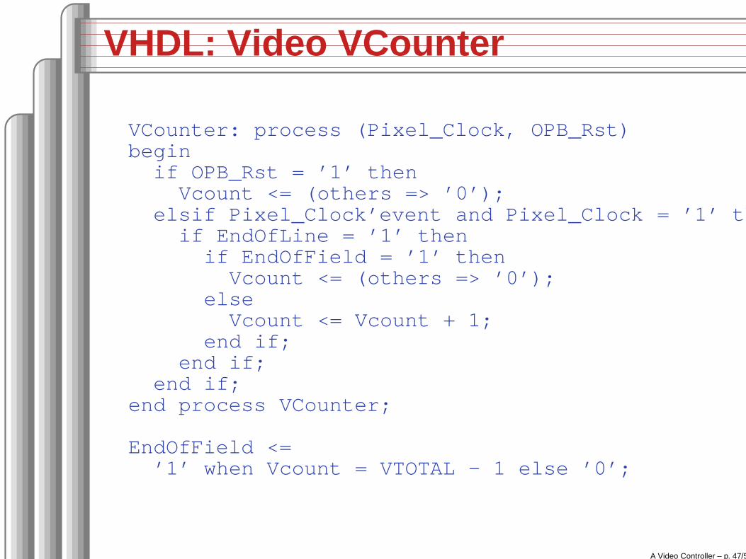
VHDL: Video VCounter
VCounter: process (Pixel_Clock, OPB_Rst)beginif OPB_Rst = ’1’ then
Vcount <= (others => ’0’);elsif Pixel_Clock’event and Pixel_Clock = ’1’ then
if EndOfLine = ’1’ thenif EndOfField = ’1’ then
Vcount <= (others => ’0’);else
Vcount <= Vcount + 1;end if;
end if;end if;
end process VCounter;
EndOfField <=’1’ when Vcount = VTOTAL - 1 else ’0’;
A Video Controller – p. 47/57
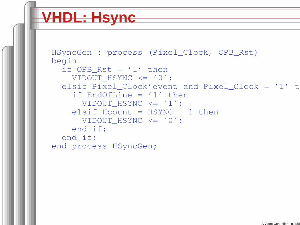
VHDL: Hsync
HSyncGen : process (Pixel_Clock, OPB_Rst)beginif OPB_Rst = ’1’ then
VIDOUT_HSYNC <= ’0’;elsif Pixel_Clock’event and Pixel_Clock = ’1’ then
if EndOfLine = ’1’ thenVIDOUT_HSYNC <= ’1’;
elsif Hcount = HSYNC - 1 thenVIDOUT_HSYNC <= ’0’;
end if;end if;
end process HSyncGen;
A Video Controller – p. 48/57
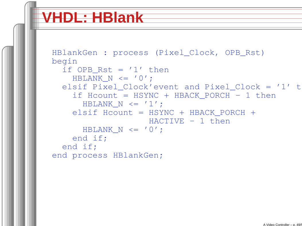
VHDL: HBlank
HBlankGen : process (Pixel_Clock, OPB_Rst)beginif OPB_Rst = ’1’ then
HBLANK_N <= ’0’;elsif Pixel_Clock’event and Pixel_Clock = ’1’ then
if Hcount = HSYNC + HBACK_PORCH - 1 thenHBLANK_N <= ’1’;
elsif Hcount = HSYNC + HBACK_PORCH +HACTIVE - 1 then
HBLANK_N <= ’0’;end if;
end if;end process HBlankGen;
A Video Controller – p. 49/57
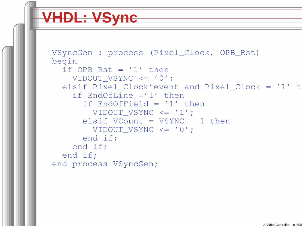
VHDL: VSync
VSyncGen : process (Pixel_Clock, OPB_Rst)beginif OPB_Rst = ’1’ then
VIDOUT_VSYNC <= ’0’;elsif Pixel_Clock’event and Pixel_Clock = ’1’ then
if EndOfLine =’1’ thenif EndOfField = ’1’ then
VIDOUT_VSYNC <= ’1’;elsif VCount = VSYNC - 1 then
VIDOUT_VSYNC <= ’0’;end if;
end if;end if;
end process VSyncGen;
A Video Controller – p. 50/57
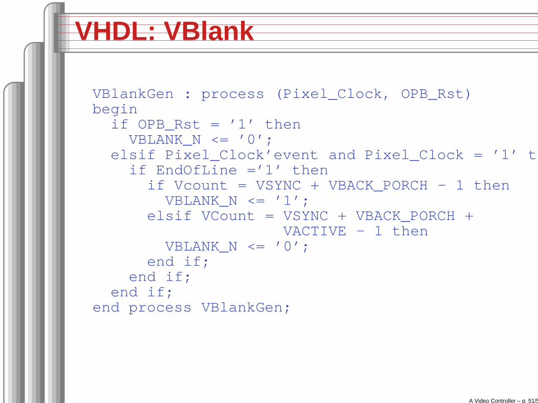
VHDL: VBlank
VBlankGen : process (Pixel_Clock, OPB_Rst)beginif OPB_Rst = ’1’ then
VBLANK_N <= ’0’;elsif Pixel_Clock’event and Pixel_Clock = ’1’ then
if EndOfLine =’1’ thenif Vcount = VSYNC + VBACK_PORCH - 1 then
VBLANK_N <= ’1’;elsif VCount = VSYNC + VBACK_PORCH +
VACTIVE - 1 thenVBLANK_N <= ’0’;
end if;end if;
end if;end process VBlankGen;
A Video Controller – p. 51/57
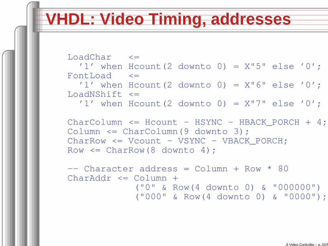
VHDL: Video Timing, addresses
LoadChar <=’1’ when Hcount(2 downto 0) = X"5" else ’0’;
FontLoad <=’1’ when Hcount(2 downto 0) = X"6" else ’0’;
LoadNShift <=’1’ when Hcount(2 downto 0) = X"7" else ’0’;
CharColumn <= Hcount - HSYNC - HBACK_PORCH + 4;Column <= CharColumn(9 downto 3);CharRow <= Vcount - VSYNC - VBACK_PORCH;Row <= CharRow(8 downto 4);
-- Character address = Column + Row * 80CharAddr <= Column +
("0" & Row(4 downto 0) & "000000") +("000" & Row(4 downto 0) & "0000");
A Video Controller – p. 52/57
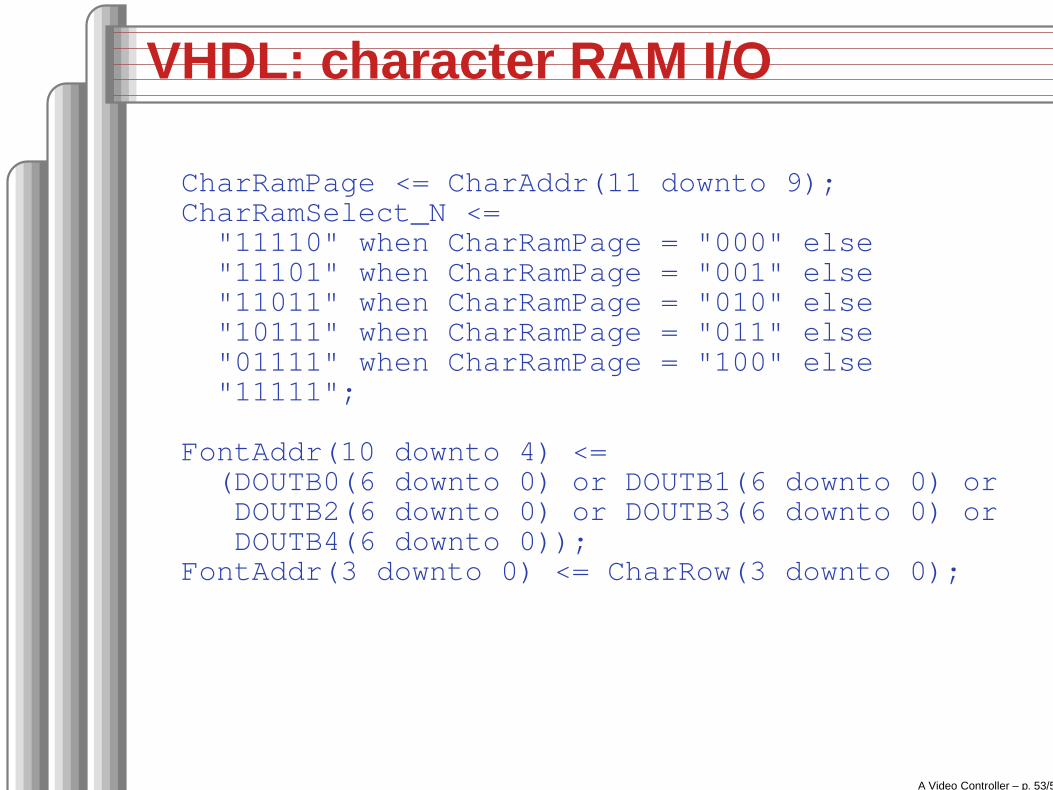
VHDL: character RAM I/O
CharRamPage <= CharAddr(11 downto 9);CharRamSelect_N <="11110" when CharRamPage = "000" else"11101" when CharRamPage = "001" else"11011" when CharRamPage = "010" else"10111" when CharRamPage = "011" else"01111" when CharRamPage = "100" else"11111";
FontAddr(10 downto 4) <=(DOUTB0(6 downto 0) or DOUTB1(6 downto 0) orDOUTB2(6 downto 0) or DOUTB3(6 downto 0) orDOUTB4(6 downto 0));
FontAddr(3 downto 0) <= CharRow(3 downto 0);
A Video Controller – p. 53/57
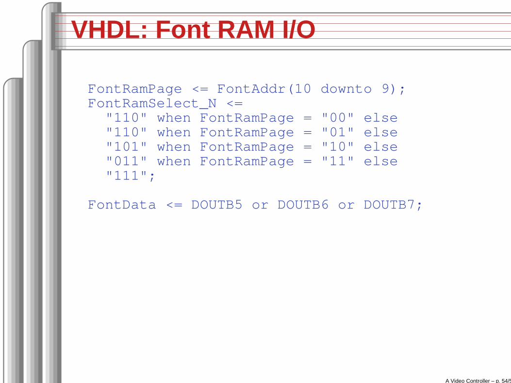
VHDL: Font RAM I/O
FontRamPage <= FontAddr(10 downto 9);FontRamSelect_N <="110" when FontRamPage = "00" else"110" when FontRamPage = "01" else"101" when FontRamPage = "10" else"011" when FontRamPage = "11" else"111";
FontData <= DOUTB5 or DOUTB6 or DOUTB7;
A Video Controller – p. 54/57
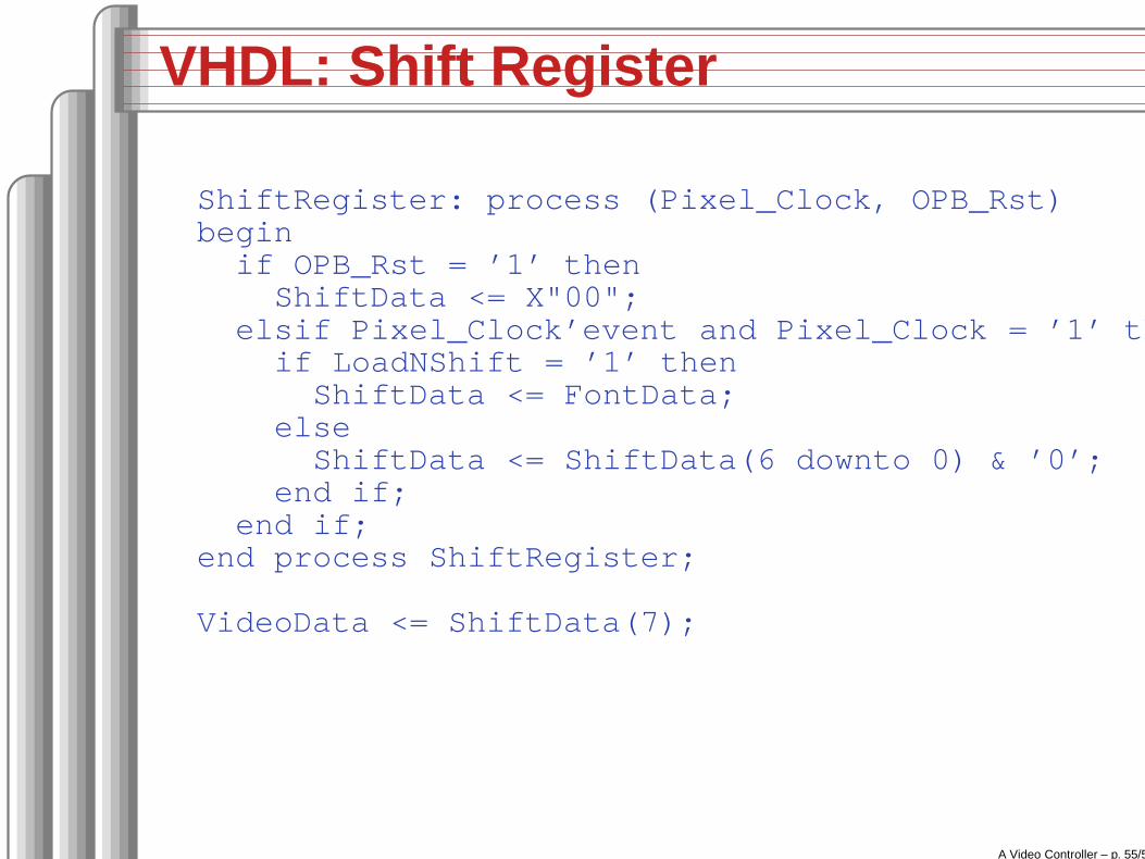
VHDL: Shift Register
ShiftRegister: process (Pixel_Clock, OPB_Rst)beginif OPB_Rst = ’1’ then
ShiftData <= X"00";elsif Pixel_Clock’event and Pixel_Clock = ’1’ then
if LoadNShift = ’1’ thenShiftData <= FontData;
elseShiftData <= ShiftData(6 downto 0) & ’0’;
end if;end if;
end process ShiftRegister;
VideoData <= ShiftData(7);
A Video Controller – p. 55/57
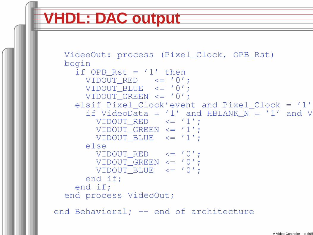
VHDL: DAC output
VideoOut: process (Pixel_Clock, OPB_Rst)begin
if OPB_Rst = ’1’ thenVIDOUT_RED <= ’0’;VIDOUT_BLUE <= ’0’;VIDOUT_GREEN <= ’0’;
elsif Pixel_Clock’event and Pixel_Clock = ’1’ thenif VideoData = ’1’ and HBLANK_N = ’1’ and VBLANK_N = ’1’ then
VIDOUT_RED <= ’1’;VIDOUT_GREEN <= ’1’;VIDOUT_BLUE <= ’1’;
elseVIDOUT_RED <= ’0’;VIDOUT_GREEN <= ’0’;VIDOUT_BLUE <= ’0’;
end if;end if;
end process VideoOut;
end Behavioral; -- end of architecture
A Video Controller – p. 56/57
The Punchline
This video controller is not quite right for theSpartan-3 chip on the Digilent boards.
Our boards have an XC3S400, which has 32K ofon-chip RAM, not 8K. The block RAMs aresimilar, but are 4K each, not 512 bytes.
What is presented here works, but is wastingmemory resources.
A better design would use only 3 of the Spartan-3block RAMS, not 8.
A Video Controller – p. 57/57