Embed Size (px)
Citation preview
To the Graduate Council: I am submitting herewith a thesis written by Jeremy Bryant Campbell entitled “A Two-Phase Cooling Method Using R134a Refrigerant to Cool Power Electronics Devices.” I have examined the final electronic copy of this thesis for form and content and recommend that it be accepted in partial fulfillment of the requirements for the degree of Master of Science, with a major in Electrical Engineering.
Leon M. Tolbert
Major Professor We have read this thesis and recommend its acceptance: Jack Lawler Syed K. Islam
Accepted for the Council:
Anne Mayhew Vice Chancellor and Dean of Graduate Studies
(Original signatures are on file with official student records.)
A Two-Phase Cooling Method Using R134a Refrigerant
to Cool Power Electronics Devices
A Thesis
Presented for the
Masters of Science
Degree
The University of Tennessee, Knoxville
Jeremy Bryant Campbell
December 2004

Copyright © 2004 by Jeremy B. Campbell
All rights reserved.
ii

Dedication
This thesis is dedicated to my family
Roger L. Campbell
Charlotte V. McKinney
Julie A. Britt and family
Jeffrey L. Campbell and family
Dad, I know you are looking down, and watching over us; we miss you!
Mom, Julie, and Jeff, Thank You for all the prayers, encouragement, and support.
iii

Acknowledgements
I would like to thank many people who supported me in finishing this thesis. First
and foremost, I would like to thank my advisor, Dr. Leon M. Tolbert for opening more
doors than I ever dreamt possible; also for your advice and genuine concern for all your
students.
I would like to thank my committee members, Drs. Jack Lawler and Syed K.
Islam.
I would like to acknowledge Donald J. Adams for the opportunity to work at Oak
Ridge National Laboratory. I would also like to thank Curtis Ayers, Burak Ozpineci,
Madhu Chinthavali, Chester Coomer, and the PEEMRC team for their valuable support.
I would like to especially thank Tony Zeind for his unwavering friendship. I
would not be here without your pep talks.
A special thanks to all my fellow colleagues at The University of Tennessee.
iv
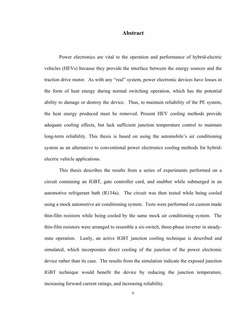
Abstract
Power electronics are vital to the operation and performance of hybrid-electric
vehicles (HEVs) because they provide the interface between the energy sources and the
traction drive motor. As with any “real” system, power electronic devices have losses in
the form of heat energy during normal switching operation, which has the potential
ability to damage or destroy the device. Thus, to maintain reliability of the PE system,
the heat energy produced must be removed. Present HEV cooling methods provide
adequate cooling effects, but lack sufficient junction temperature control to maintain
long-term reliability. This thesis is based on using the automobile’s air conditioning
system as an alternative to conventional power electronics cooling methods for hybrid-
electric vehicle applications.
This thesis describes the results from a series of experiments performed on a
circuit containing an IGBT, gate controller card, and snubber while submerged in an
automotive refrigerant bath (R134a). The circuit was then tested while being cooled
using a mock automotive air conditioning system. Tests were performed on custom made
thin-film resistors while being cooled by the same mock air conditioning system. The
thin-film resistors were arranged to resemble a six-switch, three-phase inverter in steady-
state operation. Lastly, an active IGBT junction cooling technique is described and
simulated, which incorporates direct cooling of the junction of the power electronic
device rather than its case. The results from the simulation indicate the exposed junction
IGBT technique would benefit the device by reducing the junction temperature,
increasing forward current ratings, and increasing reliability.
v
Table of Contents
CHAPTER 1...................................................................................................................... 1 INTRODUCTION ............................................................................................................... 1 1.1 TRANSPORTATION REQUIREMENTS...................................................................... 2 1.2 POWER ELECTRONICS IN HEVS ........................................................................... 4 1.3 HISTORY OF REFRIGERATION............................................................................... 6 1.4 REFRIGERATION PROCESS.................................................................................... 7 1.5 OUTLINE OF THESIS ............................................................................................. 8
CHAPTER 2.................................................................................................................... 10 HEAT SINK TECHNOLOGY ........................................................................................... 10 2.1 SEMICONDUCTOR THERMAL MODEL ................................................................. 11 2.2 POWER ELECTRONICS COOLING METHODS........................................................ 12
2.2.1 Natural Convection................................................................................... 13 2.2.2 Forced-Convection ................................................................................... 16 2.2.3 Liquid Cooled............................................................................................ 18 2.2.4 Pool Boiling .............................................................................................. 20
2.3 POWER ELECTRONICS COOLED BY R134A REFRIGERANT ................................. 23
CHAPTER 3.................................................................................................................... 24 EXPERIMENTAL RESULTS ............................................................................................ 24 3.1 LOSSES IN POWER ELECTRONICS ....................................................................... 24
3.1.1 Conduction Losses .................................................................................... 27 3.1.1.1 Piece-Wise Linear (PWL) Model ......................................................... 29 3.1.1.2 Calculating Conduction Losses............................................................. 30
3.1.2 PWL Experimental Results ....................................................................... 30 3.1.3 Switching Losses ....................................................................................... 33
3.2 EXPERIMENTAL RESULTS OF POWER DISSIPATION............................................. 34 3.2.1 Air Cooled and R134a Cooled Experimental Results............................... 34 3.2.2 Automotive R134a Air Conditioner System Results.................................. 40
3.3 SUMMARY.......................................................................................................... 47
CHAPTER 4.................................................................................................................... 48 SYSTEMS AND SIMULATION.......................................................................................... 48 4.1 THREE-PHASE INVERTER ................................................................................... 48 4.2 THIN-FILM RESISTOR......................................................................................... 51
4.2.1 Thin-Film Resistor Extrapolation............................................................. 56 4.3 ACTIVE IGBT JUNCTION COOLING SIMULATION ............................................... 58
4.3.1 Single IGBT Simulation ............................................................................ 59 4.4 SUMMARY.......................................................................................................... 62
CHAPTER 5.................................................................................................................... 64 CONCLUSION AND FUTURE WORK .............................................................................. 64
vi

5.1 CONCLUSION...................................................................................................... 64 5.2 FUTURE WORK .................................................................................................. 65
LIST OF REFERENCES............................................................................................... 67
APPENDICES................................................................................................................. 70
APPENDIX I ................................................................................................................... 71
APPENDIX II.................................................................................................................. 79
APPENDIX III ................................................................................................................ 80
VITA................................................................................................................................. 81
vii
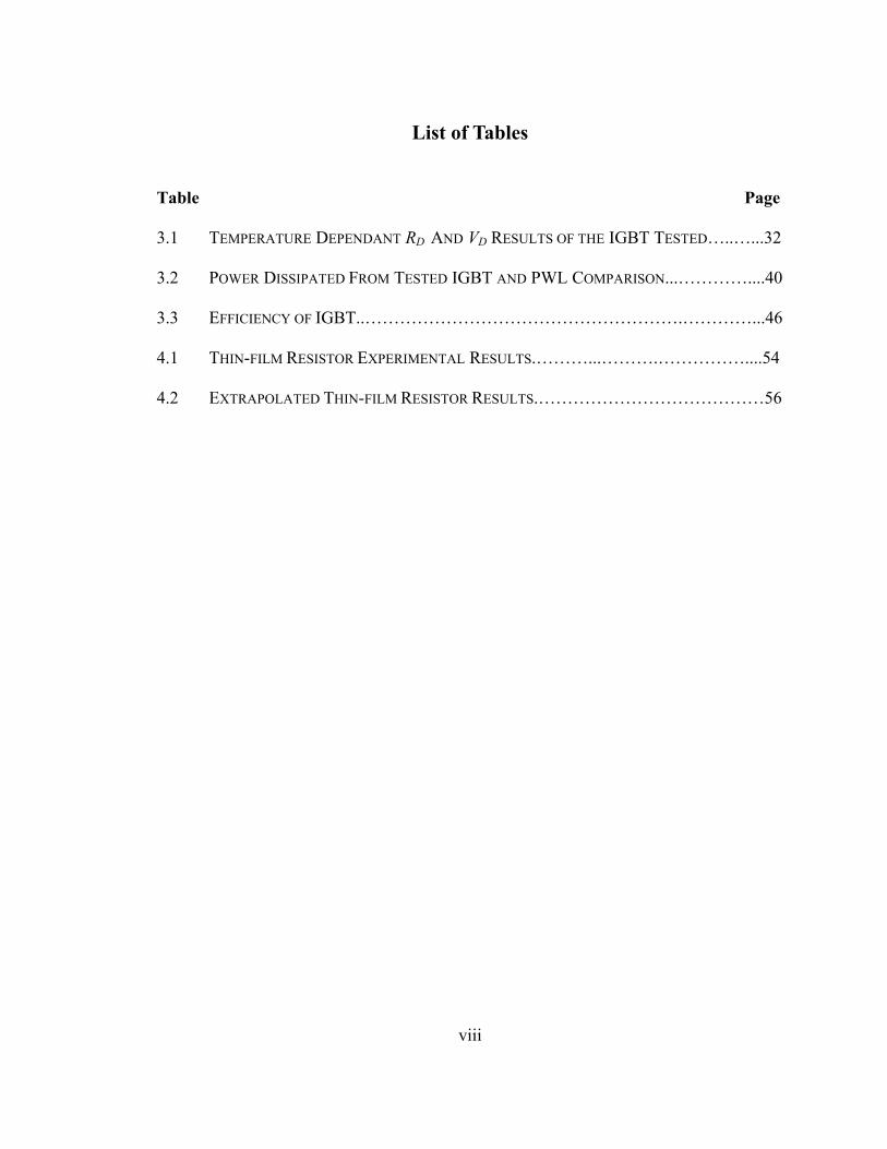
List of Tables
Table Page 3.1 TEMPERATURE DEPENDANT RD AND VD RESULTS OF THE IGBT TESTED…..…...32
3.2 POWER DISSIPATED FROM TESTED IGBT AND PWL COMPARISON...…………....40
3.3 EFFICIENCY OF IGBT..……………………………………………….…………...46
4.1 THIN-FILM RESISTOR EXPERIMENTAL RESULTS.………...……….……………....54
4.2 EXTRAPOLATED THIN-FILM RESISTOR RESULTS.…………………………………56
viii
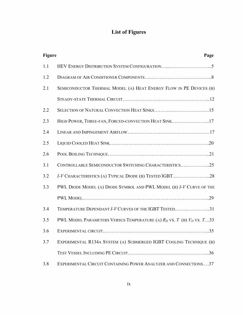
List of Figures
Figure Page 1.1 HEV ENERGY DISTRIBUTION SYSTEM CONFIGURATION…...……………………...5
1.2 DIAGRAM OF AIR CONDITIONER COMPONENTS…..………………………………..8
2.1 SEMICONDUCTOR THERMAL MODEL (A) HEAT ENERGY FLOW IN PE DEVICES (B)
STEADY-STATE THERMAL CIRCUIT……….…………………………….………...12
2.2 SELECTION OF NATURAL CONVECTION HEAT SINKS……….………………….…15
2.3 HIGH POWER, THREE-FAN, FORCED-CONVECTION HEAT SINK.…………………..17
2.4 LINEAR AND IMPINGEMENT AIRFLOW….…………………………………………17
2.5 LIQUID COOLED HEAT SINK….…………………………………………………..20
2.6 POOL BOILING TECHNIQUE…………………..…………………………………...21
3.1 CONTROLLABLE SEMICONDUCTOR SWITCHING CHARACTERISTICS….…………...25
3.2 I-V CHARACTERISTICS (A) TYPICAL DIODE (B) TESTED IGBT....………………...28
3.3 PWL DIODE MODEL (A) DIODE SYMBOL AND PWL MODEL (B) I-V CURVE OF THE
PWL MODEL……………………………………………………………………..29
3.4 TEMPERATURE DEPENDANT I-V CURVES OF THE IGBT TESTED……...…………..31
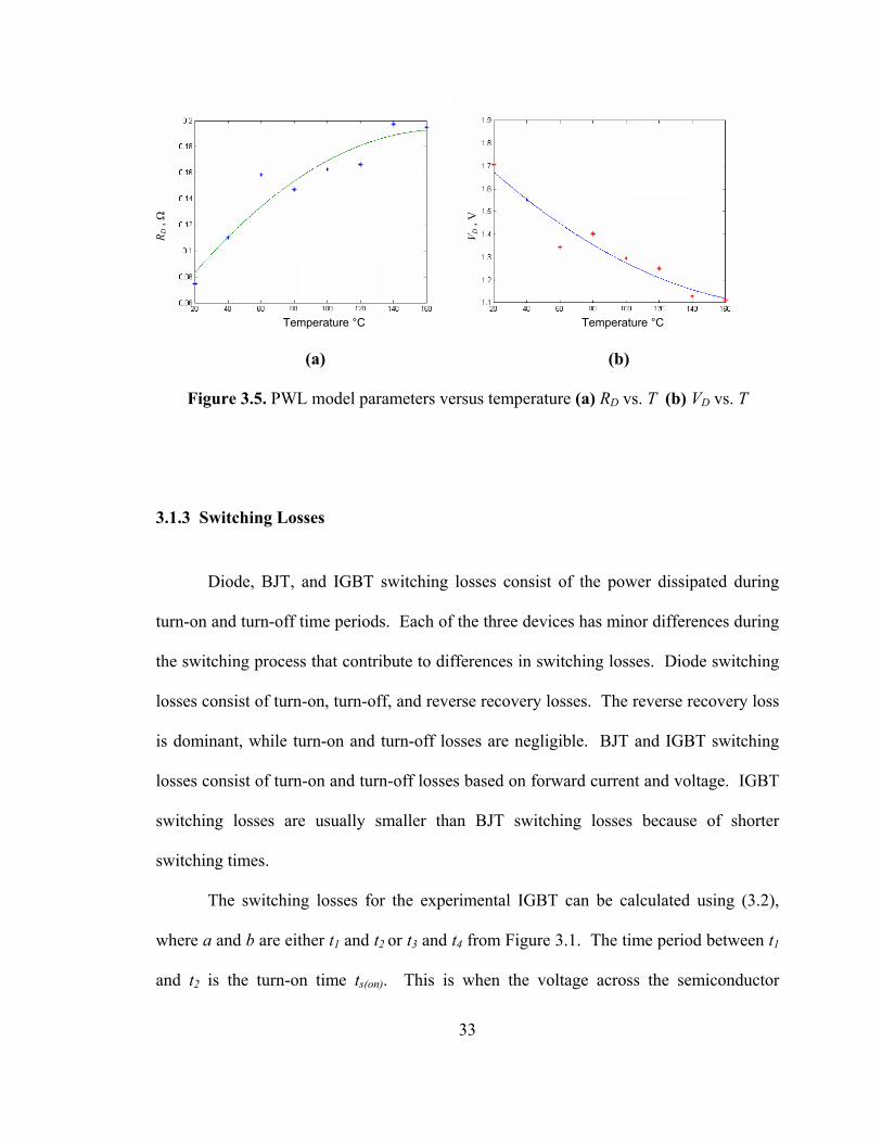
3.5 PWL MODEL PARAMETERS VERSUS TEMPERATURE (A) RD VS. T (B) VD VS. T....33
3.6 EXPERIMENTAL CIRCUIT..………………………………………………………...35
3.7 EXPERIMENTAL R134A SYSTEM (A) SUBMERGED IGBT COOLING TECHNIQUE (B)
TEST VESSEL INCLUDING PE CIRCUIT……….…………………………………...36
3.8 EXPERIMENTAL CIRCUIT CONTAINING POWER ANALYZER AND CONNECTIONS.…37
ix
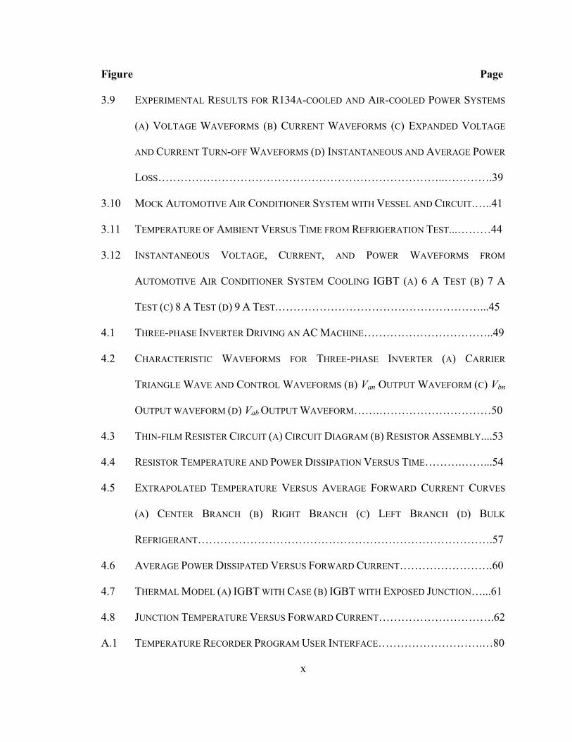
Figure Page
3.9 EXPERIMENTAL RESULTS FOR R134A-COOLED AND AIR-COOLED POWER SYSTEMS
(A) VOLTAGE WAVEFORMS (B) CURRENT WAVEFORMS (C) EXPANDED VOLTAGE
AND CURRENT TURN-OFF WAVEFORMS (D) INSTANTANEOUS AND AVERAGE POWER
LOSS…………………………………………………………………..………….39
3.10 MOCK AUTOMOTIVE AIR CONDITIONER SYSTEM WITH VESSEL AND CIRCUIT.…..41
3.11 TEMPERATURE OF AMBIENT VERSUS TIME FROM REFRIGERATION TEST...………44
3.12 INSTANTANEOUS VOLTAGE, CURRENT, AND POWER WAVEFORMS FROM
AUTOMOTIVE AIR CONDITIONER SYSTEM COOLING IGBT (A) 6 A TEST (B) 7 A
TEST (C) 8 A TEST (D) 9 A TEST.………………………………………………...45
4.1 THREE-PHASE INVERTER DRIVING AN AC MACHINE……………………………..49
4.2 CHARACTERISTIC WAVEFORMS FOR THREE-PHASE INVERTER (A) CARRIER
TRIANGLE WAVE AND CONTROL WAVEFORMS (B) Van OUTPUT WAVEFORM (C) Vbn
OUTPUT WAVEFORM (D) Vab OUTPUT WAVEFORM…….…………………………50
4.3 THIN-FILM RESISTER CIRCUIT (A) CIRCUIT DIAGRAM (B) RESISTOR ASSEMBLY....53
4.4 RESISTOR TEMPERATURE AND POWER DISSIPATION VERSUS TIME……….……...54
4.5 EXTRAPOLATED TEMPERATURE VERSUS AVERAGE FORWARD CURRENT CURVES
(A) CENTER BRANCH (B) RIGHT BRANCH (C) LEFT BRANCH (D) BULK
REFRIGERANT…………………………………………………………………….57
4.6 AVERAGE POWER DISSIPATED VERSUS FORWARD CURRENT…………………….60
4.7 THERMAL MODEL (A) IGBT WITH CASE (B) IGBT WITH EXPOSED JUNCTION…...61
4.8 JUNCTION TEMPERATURE VERSUS FORWARD CURRENT………………………….62
A.1 TEMPERATURE RECORDER PROGRAM USER INTERFACE……………………….…80
x
Chapter 1
INTRODUCTION
Electric cars have been an option since the beginning of the automobile
revolution. Early electric vehicles were mechanically robust, but lacking horsepower
because of poor battery technology. Thus, the internal combustion (IC) engine quickly
became the best power plant for the automobile because petroleum fuel was a superior
source of energy. Petroleum fuel was chosen due to its high-energy density properties,
ease of handling, and cheap abundant supplies.
Today, more than 100 years later, cities have become choked with combustion by-
products of petroleum, and the world’s dependence on petroleum continues to increase,
while petroleum deposits are diminishing. Consequently, these concerns are renewing
interest for alternative energy sources in the transportation industry. While there are
many options, the electric and hybrid electric vehicles (EV/HEV) are the most promising
alternatives to the IC powertrain as these options maintain the automotive industry, which
helps the world’s economy thrive. This renewed interest has recently spurred the Toyota
PriusTM and Honda InsightTM. These HEVs are the first HEVs to make production.
Power electronics (PEs) are vital to the operation and performance of EVs and
HEVs. Power electronics provide the interface between the energy sources such as
batteries and the traction drive motor. PEs must meet strict automobile manufacturers’
design criteria when used in EVs and HEVs. The four most import design criteria for the
automotive industry are weight, size, reliability, and cost.
1
The thermal management system for power electronics devices plays an important
role in all four design criteria. PEs capabilities are highly temperature dependent. To
maintain reliability of PE systems, the temperature must be strictly regulated. If the
temperature is allowed to vary, the PE devices must be oversized for their typical
application in order to meet every operating condition. Existing thermal management
designs rely mainly upon oversizing the PEs as just described or by inclusion of large
heat sinks, both of which detract from the size and cost criteria of automotive design
criteria. Present thermal management techniques for power electronics cannot meet all
the requirements of the transportation industry. However, existing air-conditioning (A/C)
systems in automobiles with little modification can be used to cool PE devices.
Utilization of the existing A/C systems to directly cool the PEs can help meet the design
criteria described previously.
This thesis describes a new technique of directly submerging PEs in a vehicle’s
refrigerant (R134a) as an active method to cool power electronic devices. This technique
is shown to meet the demanding requirements of the automotive industry. This technique
will be discussed in the next sections with specific application to the HEV systems.
1.1 Transportation Requirements
In an effort to increase HEV development, the United States Department of Energy
(DOE) has partnered with automotive manufacturers, universities, national laboratories,
and various industry leaders in a program called the FreedomCAR (Cooperative
Automotive Research). The goal of this partnership is to share technology in an effort to
2
develop more energy efficient and environmentally friendly highway transportation
technologies. In turn, the transportation industry will provide these technologies to the
consumers in the least amount of time. To meet these goals, the technology must first be
developed. Outlining the efforts for the FreedomCAR partners are the following design
requirements:
• Electric propulsion systems, electric motor and inverter, with a 15-year life
capable of delivering at least 55 kW of power for 18 seconds and 30 kW of
continuous power at a system cost of $12/kW peak.
• Electric propulsion system having a coolant inlet temperature of 105ºC.
• Electric drivetrain energy storage with a 15-year life with discharge power of 25
kW for 18 seconds and $20/kW.
• Material and manufacturing technologies for high-volume production vehicles
that provides 50% reduction in the weight of vehicle structure and subsystems,
affordably, and increased use of recyclable/renewable materials.
Thermal management technology of power electronics devices has a direct impact on
all the above design requirements. An effective, small, lightweight thermal management
system will contribute to greater efficiency and reliability of the power electronics
devices. In turn, a lighter vehicle results in less demand on the engine and/or motor,
faster acceleration, and greater energy efficiency. Higher energy efficiency contributes to
less fuel or battery consumption.
3
1.2 Power Electronics in HEVs
Simplistically, power electronics are responsible for the process and controlled flow
of electric energy by supplying voltages and currents in a form that is optimally suited for
user loads [1]. In HEVs, PEs are the interface between the energy sources and the
traction drive motor for both power consumption and regenerative cases. Figure 1.1
shows a HEV’s typical configuration. As shown in the figure, PEs allow the HEV to
operate as they connect the batteries to the motor and generator (in some cases these may
be the same devices) allowing the vehicle to function.
Driving conditions vary from flat interstate cruising to start and stop city driving.
The most severe driving conditions require hard acceleration and braking. These
conditions force power electronics to their extreme limits such that they must conduct
high forward biased currents, block high forward and reverse voltages, cycle on and off
within microseconds, and resist thermal breakdown because of external environmental
conditions and their own internally produced heat.
Severe driving conditions can force the traction motors to exceed 100 Amps peak and
80 Amps continuous. The forward and reverse voltage blocking capabilities of PEs can
greatly exceed 300 Volts; yet using PEs with higher voltage blocking capabilities will
minimize the need to configure multiple devices in series, thus lowering on-state voltages
and conduction losses. PE devices must also be required to have fast turn-on and turn-off
transitions, yet they must have small dv/dt and di/dt to minimize switching losses. An
increase in switching cycles will increase power losses.
4
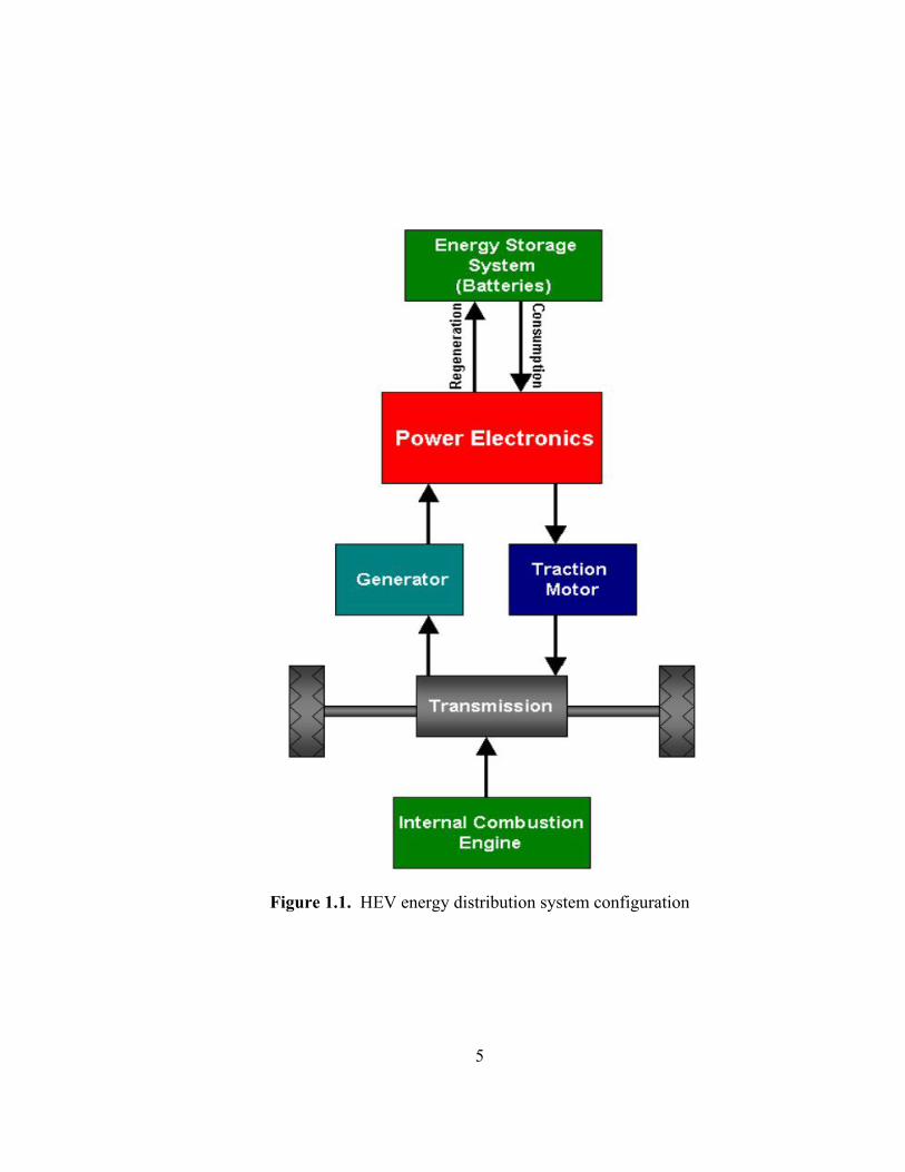
Figure 1.1. HEV energy distribution system configuration
5

Traditional automobiles as well as HEVs produce temperatures over 105°C in the
engine compartment due mainly to the IC engine heat dissipation. Unfortunately, this is
the ideal physical location for most power electronics devices as it offers some
environmental protection (rain, debris, etc), space for mounting, minimizes stray
inductance, and is the location of existing A/C systems thus helping to minimize the
additional PE load to A/C system.
1.3 History of Refrigeration
The definition of air conditioning is the control of temperature, humidity, purity,
and motion of air in an enclosed space, independent of outside air conditions [2].
Refrigeration or air conditioning was first widely introduced in the late 1800s in the form
of household refrigerators for food product storage. Soon air conditioning usage was
expanded to cooling homes and business. Eventually in the 1950s, automobiles started
becoming equipped with A/C systems. Today, nearly all of new automobiles sold in the
US are equipped with an A/C system, becoming more of a standard rather than a luxury.
The first refrigerators began by using a toxic mixture of refrigerant that included
ammonia (NH3) and methyl chloride (CH3Cl). This mixture is toxic to people if the
system were to leak, so in 1928, a non-toxic replacement refrigerant called Freon was
invented. However, the Environmental Protection Agency (EPA) has determined that
chlorofluorocarbons (CFCs) based refrigerants such as Freon, are harmful to the
environment. It was determined that these refrigerants are a major contributor to the
depletion of the earth’s ozone layer. The “Montreal Protocol,” an international
6
agreement, established a plan to reduce emissions of CFCs and was signed by a total of
24 nations in September of 1987. Since 1993, Tetrafluoroethane (R134a) has become the
environmentally friendly replacement to Freon in automobiles. R134a’s prevalent usage
in A/C systems and ideal thermal properties makes it ideal for use as an active coolant for
PE devices in HEV applications.
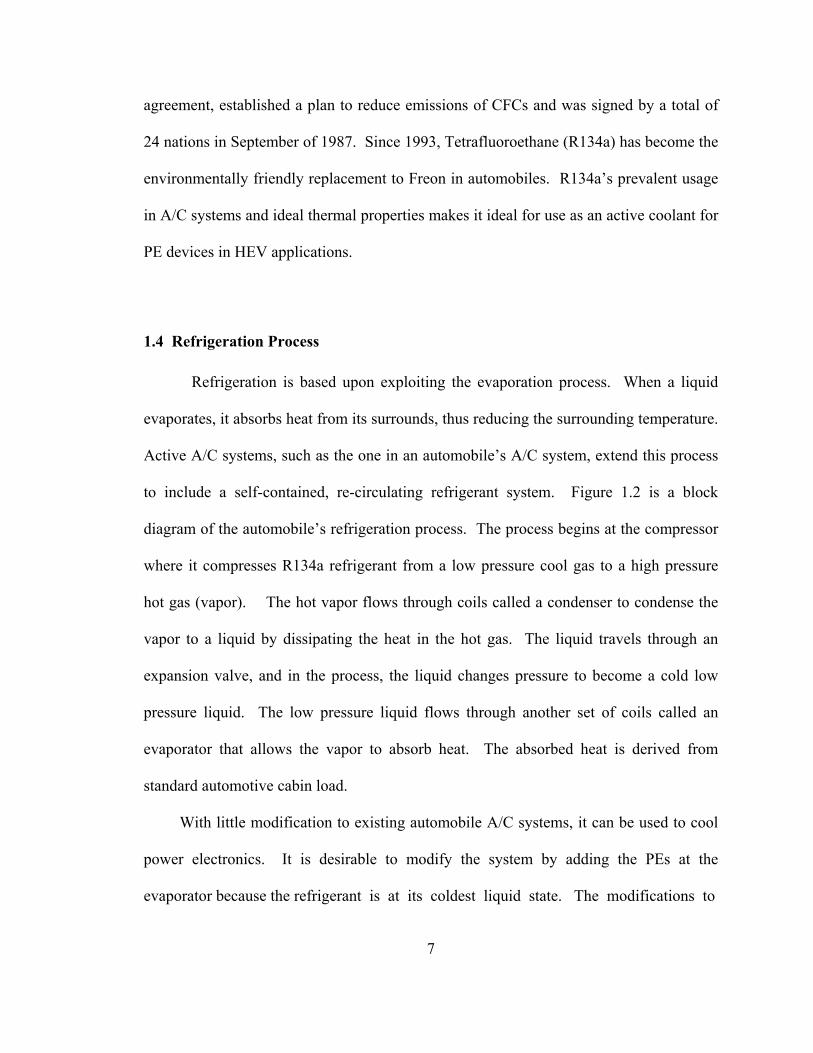
1.4 Refrigeration Process
Refrigeration is based upon exploiting the evaporation process. When a liquid
evaporates, it absorbs heat from its surrounds, thus reducing the surrounding temperature.
Active A/C systems, such as the one in an automobile’s A/C system, extend this process
to include a self-contained, re-circulating refrigerant system. Figure 1.2 is a block
diagram of the automobile’s refrigeration process. The process begins at the compressor
where it compresses R134a refrigerant from a low pressure cool gas to a high pressure
hot gas (vapor). The hot vapor flows through coils called a condenser to condense the
vapor to a liquid by dissipating the heat in the hot gas. The liquid travels through an
expansion valve, and in the process, the liquid changes pressure to become a cold low
pressure liquid. The low pressure liquid flows through another set of coils called an
evaporator that allows the vapor to absorb heat. The absorbed heat is derived from
standard automotive cabin load.
With little modification to existing automobile A/C systems, it can be used to cool
power electronics. It is desirable to modify the system by adding the PEs at the
evaporator because the refrigerant is at its coldest liquid state. The modifications to
7
Figure 1.2. Diagram of air conditioner components
existing automotive A/C systems would require two extra refrigerant tubes and a pressure
vessel to hold the PEs. One tube is used to divert the liquid refrigerant to the vessel
containing the power electronics equipment, and the second tube is used as a return.
Automobile manufacturers will benefit from this approach by reducing cost and weight of
the vehicle.
1.5 Outline of Thesis
The objective of this thesis is to investigate and evaluate a two-phase cooling
method using R134a refrigerant to dissipate the heat energy generated by the rectifiers,
converters, and inverters of PEs used in HEV application.
8

First, a silicon IGBT current vs. voltage characteristics will be modeled. Then, an
evaluation of the IGBT submerged in R134a to identify advantages of the proposed
cooling method over conventional cooling methods will be conducted. Last, a system
study of an inverter cooled by a vehicle’s air conditioning system is conducted to provide
an increase in energy efficiency and reliability.
Chapter 2 is a summary of existing thermal management techniques with several
examples.
Chapter 3 explains the approach used to characterize and model the IGBT, evaluate
power dissipation, and study the effects R134a refrigerant on power electronics devices.
Chapter 4 discusses the thermal model and applies it to an automotive application.
Chapter 5 provides conclusions and recommendations.
9
Chapter 2
HEAT SINK TECHNOLOGY
In past years, electrical devices that delivered significant levels of power were
typically packaged with large enclosures to house large heat sinks or base plates. No
formal method, other than experience, was widely used for predicting the size of the heat
sink required to maintain a particular device temperature and operating life.
Consequently, the solution to maintain an operating temperature became one of using the
largest heat sink and enclosure, a brute force solution. While this method is adequate for
previous PE generations, present day power electronics are smaller, conduct more
current, and generate larger heat densities, where the current cooling requirements are
more complex and cannot generally be solved with a simple aluminum mass.
This chapter begins by establishing a semiconductor thermal model where heat
energy is calculated by formulas similar to Ohm’s Law. The remainder of the chapter is
dedicated to four thermal management systems commonly used by engineers today.
These include natural convection, forced-convection, liquid cooled, and pool boiling.
Each system has their own set of advantages and disadvantages all of which will be
explored in some detail.
10
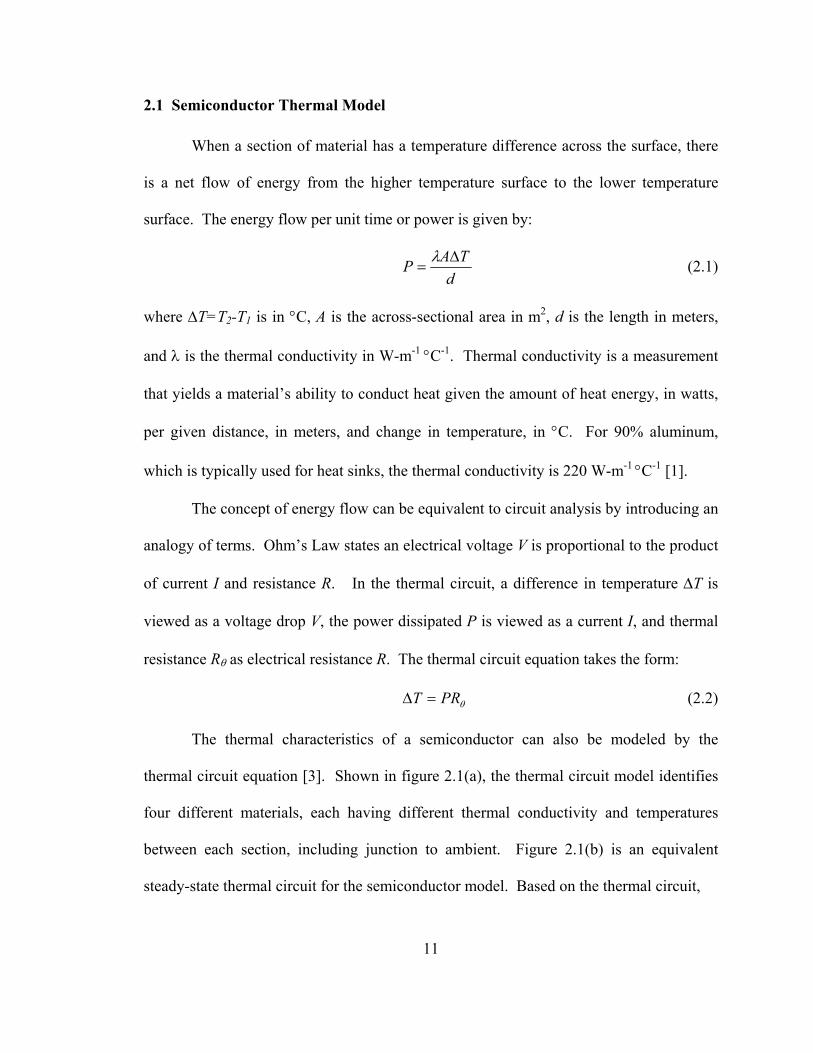
2.1 Semiconductor Thermal Model
When a section of material has a temperature difference across the surface, there
is a net flow of energy from the higher temperature surface to the lower temperature
surface. The energy flow per unit time or power is given by:
dTAP ∆
=λ (2.1)
where ∆T=T2-T1 is in °C, A is the across-sectional area in m2, d is the length in meters,
and λ is the thermal conductivity in W-m-1 °C-1. Thermal conductivity is a measurement
that yields a material’s ability to conduct heat given the amount of heat energy, in watts,
per given distance, in meters, and change in temperature, in °C. For 90% aluminum,
which is typically used for heat sinks, the thermal conductivity is 220 W-m-1 °C-1 [1].
The concept of energy flow can be equivalent to circuit analysis by introducing an
analogy of terms. Ohm’s Law states an electrical voltage V is proportional to the product
of current I and resistance R. In the thermal circuit, a difference in temperature ∆T is
viewed as a voltage drop V, the power dissipated P is viewed as a current I, and thermal
resistance Rθ as electrical resistance R. The thermal circuit equation takes the form:
θPRT =∆ (2.2)
The thermal characteristics of a semiconductor can also be modeled by the
thermal circuit equation [3]. Shown in figure 2.1(a), the thermal circuit model identifies
four different materials, each having different thermal conductivity and temperatures
between each section, including junction to ambient. Figure 2.1(b) is an equivalent
steady-state thermal circuit for the semiconductor model. Based on the thermal circuit,
11
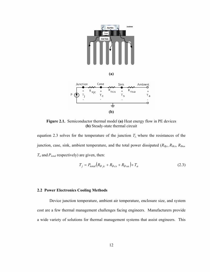
(a)
(b)
Figure 2.1. Semiconductor thermal model (a) Heat energy flow in PE devices
(b) Steady-state thermal circuit
equation 2.3 solves for the temperature of the junction Tj, where the resistances of the
junction, case, sink, ambient temperature, and the total power dissipated (Rθjc, Rθcs, Rθsa,
Ta and Ptotal respectively) are given, then:
( ) asacsjctotalj TRRRPT +++= θθθ (2.3)
2.2 Power Electronics Cooling Methods
Device junction temperature, ambient air temperature, enclosure size, and system
cost are a few thermal management challenges facing engineers. Manufacturers provide
a wide variety of solutions for thermal management systems that assist engineers. This
12
section will investigate four of the most popular among industry, then comment on each
system’s advantages and disadvantages for HEV applications.
2.2.1 Natural Convection
Natural convection or air-cooling is still widely used, and will always be favored
whenever possible, as it is the least expensive of all cooling systems [4]. However,
directly cooling PEs by mere ambient air alone is typically not enough to keep the
junction temperature below the manufacturer’s recommended level. Thus, PEs must be
mounted on heat sinks, typically aluminum. Aluminum provides adequate thermal
conductivity, reduced weight, and reduced cost when compared to materials such copper
or steel [5].
There are two main parts that comprise a heat sink, base plate and fins. The base
plate has three responsibilities:
1. Provide a surface where the PE devices are attached
2. Structural rigidity to the system
3. Spread heat away from the PE to the fins.
Engineers must compromise between the proper heat spreading and conduction losses
within the base plate. A base plate that is too thick will have minimum conduction
losses, but heat spreading in the lateral direction will decrease, resulting in a lower
system thermal efficiency and excessive weight. A base plate too thin will obtain an
increase in heat spreading, but an increase in conduction losses and lack the structural
rigidity need for self support and support for mounted PEs. The optimum base plate
13
thickness is governed by the number of PE devices, the surface area covered by each
device, the mechanical requirements for device mounting, and the circuit application. A
circuit application in steady-state mode is cooled best with a thin base plate and a large
number of fins along the width, while a circuit application in impulse mode is cooled best
with a thicker base plate and reduced amount of fins across the width [5].
Fins are constructed of thin vertical plates of metal welded or machined to the
base plate and provide deep channels for an increase in surface area to assist convective
cooling. The fins have constraints for height and spacing, where altering one will cause
the performance of the fin to change. Increasing the height of the fin beyond the point
where the fin temperature reaches ambient temperature provides no useful purpose. Fin
spacing determines the airflow across the fin surface. Movement of air molecules by
natural convection is induced when a surface is at an elevated temperature above
ambient. Then as air molecules pass by the fin surface, heat energy is transferred to the
air. As fin spacing decreases, less air can pass across the fin surface and no heat energy
is transferred. On the other hand, as the fin spacing increases, fewer fins exist, thus
reducing the convective heat transfer.
Additional advantages of natural convection heat sinks are no moving parts and a
large selection from manufacturers. No moving parts greatly increase reliability and
reduce cost of the cooling system. Multiple options exist for most power levels and
enclosure types giving design engineers flexibility to choose a heat sink that best fits their
design application. Figure 2.2 is an example of 12 different natural convection heat sinks
including a table of corresponding thermal resistance and volume specifications for each.
The thermal resistance Rθsa measured in °C/W is the theoretical resistance between the
14
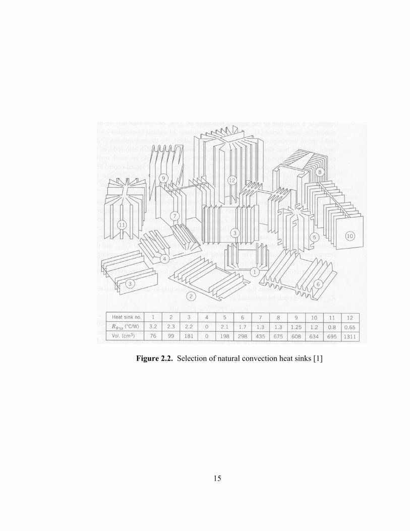
Figure 2.2. Selection of natural convection heat sinks [1]
15
heat sink and the ambient air, which determines how much heat energy is dissipated to
the ambient air. The volume of each heat sink is measured in cm3, and this measurement
is used to determine the enclosure requirements.
Engineers must keep in mind that the cooling capability of natural convection heat
sinks is heavily dependant upon the ambient temperature and a clean fin surface. Dirt,
dust, and related matter can also deteriorate the heat sink’s cooling capability by retaining
excessive heat energy and increasing the thermal resistance Rsa. As the surrounding air
temperature increases, the cooling capability decreases, because less heat can be absorbed
by the surrounding environment. R-theta® designs all natural convection heat sinks for
optimum performance at 50°C above ambient [5].
2.2.2 Forced-Convection
Because air has such poor thermal transport properties, forced circulation is often
required to enhance the heat dissipation process in natural convection heat sinks [4]. Air
is forced across the fin surface by use of a fan. This lowers the thermal resistance Rθsa
and enables the heat sink to disperse more heat. Forced-convection heat sinks can
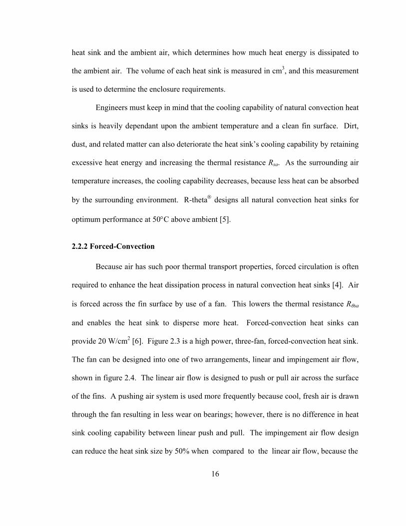
provide 20 W/cm2 [6]. Figure 2.3 is a high power, three-fan, forced-convection heat sink.
The fan can be designed into one of two arrangements, linear and impingement air flow,
shown in figure 2.4. The linear air flow is designed to push or pull air across the surface
of the fins. A pushing air system is used more frequently because cool, fresh air is drawn
through the fan resulting in less wear on bearings; however, there is no difference in heat
sink cooling capability between linear push and pull. The impingement air flow design
can reduce the heat sink size by 50% when compared to the linear air flow, because the
16
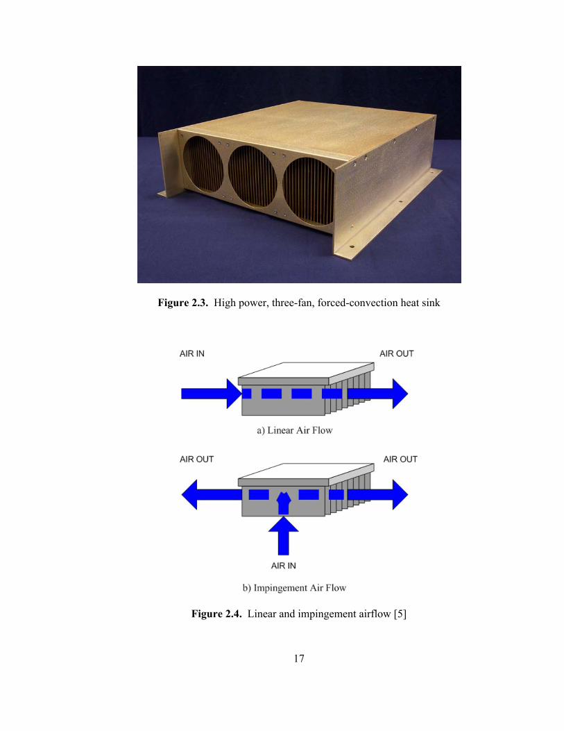
Figure 2.3. High power, three-fan, forced-convection heat sink
Figure 2.4. Linear and impingement airflow [5]
17
free air area of the fin is doubled [5]. By design, the air in the impingement air flow
system has a shorter distance to travel and a larger volume of flow resulting in a lower
temperature difference between a fin’s beginning (side closest to the air in) and end (side
closest to the air out) [7].
The advantages of forced-convection heat sinks are smaller size, lighter weight,
and more efficient compared to natural convection heat sinks. These advantages enable
engineers to design PEs to be placed in smaller enclosures, which reduce the system’s
overall size, weight, and possibly the cost. The fan is usually a low current device
drawing no more than 0.25 A and 30 W, which is only a fraction of the total power
dissipated by the heat sink.
Natural convection and forced-convection heat sinks are not capable of meeting
HEV demands on power electronics [8]. Excessive ambient temperatures and dirty
conditions in the engine compartment will likely cause a decrease in efficiency and
ultimately lead to the premature failure of the PE devices. Also, any air-cooled heat sink
designed for HEV application would require an excessive mass of aluminum, much
larger and heavier than an HEV application could conveniently accept.
2.2.3 Liquid Cooled
Liquid cooling is designed to exploit the excellent thermal conductivity properties
of liquids such as water and ethylene glycol known as coolants. The thermal
conductivity of water is 0.60 W-m-1K-1, which makes it one of the best thermal
conductors among all liquids. Unfortunately, water has poor dielectric characteristics
that contribute to short circuits and electrical equipment failure.
18
Traditionally, the solution to separating the liquid from the electrical devices is to
contain the liquid in a closed loop system, where the liquid does not contact the device,
but rather the substrate upon which the device is mounted. The components needed for
liquid cooling are comprised of a heat sink, piping, liquid pump, and a condenser. A
liquid cooled heat sink differs from an air cooled heat sink in the construction. The liquid
cooled heat sink has cavities that channels water through the heat sink, absorbing the
sink’s heat, and then discharging the water without the liquid physically contacting the
device.
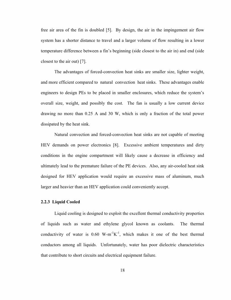
The process of liquid cooling PEs, shown in Figure 2.5, involves a coolant
entering the heat sink, which houses the semiconductors. Heat is conducted away from
the semiconductor through the heat sink and absorbed by the coolant. Then, the coolant
travels out of the heat sink through a pipe, and enters the condenser. Last, the hot coolant
travels through the condenser where the heat from the water is dissipated to the
surrounding air, before being cycled through the entire system repetitively.
Liquid cooling reduces the thermal resistance between the semiconductor case
and ambient air, implying a greater heat transfer. Heat flux of 100 W/cm2 can be
achieved, well beyond the ability of forced-air heat sinks [6]. Presently, HEVs use a
liquid cooled heat sink with an ethylene glycol based coolant [9,10]. Based on
FreedomCAR requirements for maximum liquid temperature of 105°C, the coolant loop
is separate from the liquid loop used to cool the IC engine.
19
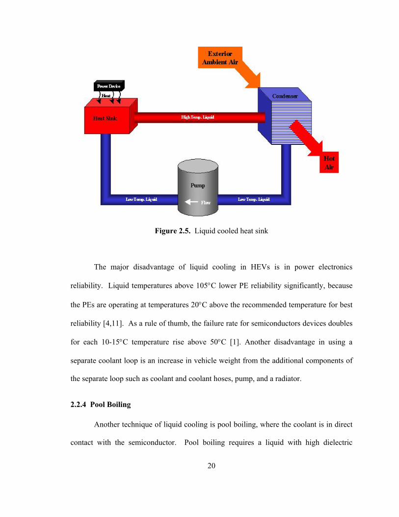
Figure 2.5. Liquid cooled heat sink
The major disadvantage of liquid cooling in HEVs is in power electronics
reliability. Liquid temperatures above 105°C lower PE reliability significantly, because
the PEs are operating at temperatures 20°C above the recommended temperature for best
reliability [4,11]. As a rule of thumb, the failure rate for semiconductors devices doubles
for each 10-15°C temperature rise above 50°C [1]. Another disadvantage in using a
separate coolant loop is an increase in vehicle weight from the additional components of
the separate loop such as coolant and coolant hoses, pump, and a radiator.
2.2.4 Pool Boiling
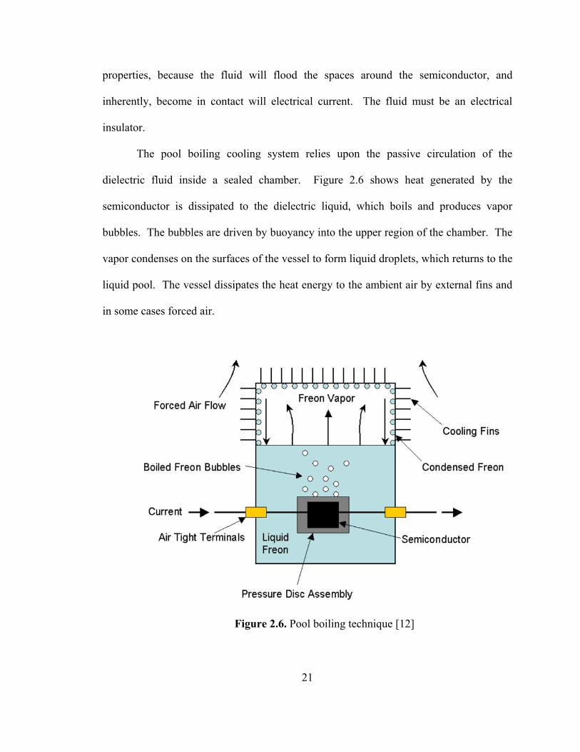
Another technique of liquid cooling is pool boiling, where the coolant is in direct
contact with the semiconductor. Pool boiling requires a liquid with high dielectric
20
properties, because the fluid will flood the spaces around the semiconductor, and
inherently, become in contact will electrical current. The fluid must be an electrical
insulator.
The pool boiling cooling system relies upon the passive circulation of the
dielectric fluid inside a sealed chamber. Figure 2.6 shows heat generated by the
semiconductor is dissipated to the dielectric liquid, which boils and produces vapor
bubbles. The bubbles are driven by buoyancy into the upper region of the chamber. The
vapor condenses on the surfaces of the vessel to form liquid droplets, which returns to the
liquid pool. The vessel dissipates the heat energy to the ambient air by external fins and
in some cases forced air.
Figure 2.6. Pool boiling technique [12]
21
Pool boiling is one of the most efficient techniques to remove heat from a device
[13]. Heat flux for pool boiling can exceed 100 W/cm2; at this rate, more heat energy can
be dissipated in less area than any previous thermal management techniques discussed
previously [6]. Additional advantages of pool boiling include a decrease in the size and
weight of the cooling system, and the PEs are isolated from external contaminants such
as dust and dirt as this too is a closed system [12,14].
The disadvantages of employing pool boiling cooling systems to an HEV
application include a limited selection of dielectric fluids and contamination collection on
vessel cooling fins from the engine compartment. Intimate contact of the liquid with the
device places stringent chemical and electrical compatibility constraints, limiting the
choice of coolant to a select few. One choice is CFCs based refrigerants; however, these
fluids are harmful to the environment and are banned by governmental laws. Another
choice for a dielectric fluid is FC-72, more commonly known as Fluorinert. Fluorinert is
manufactured by the 3M™ company, and designed to be a pool boiling refrigerant. It
possesses high dielectric characteristics and has similar thermal conductivity
characteristics to CFCs based refrigerants [11,12]. Additional fluids exist yet fail to be
successful enough to be considered.
Pool boiling cooling systems containing CFCs based refrigerants were used in
traction drive and various motor drives applications before the governmental ban [12,14].
Pool boiling cooling systems containing Fluorinert are currently in development for high
power electronic chip applications [4,6,13].
22

2.3 Power Electronics Cooled By R134a Refrigerant
In the next chapter, cooling power electronic devices by submerging the devices
in R134a refrigerant is considered. Experimental tests on a submerged and air-cooled
IGBT and gate-controller card to study the R134a dielectric characteristics, deterioration
effects, and heat flux capacity are conducted and results are presented.
23
Chapter 3
EXPERIMENTAL RESULTS
Power electronics devices inherently produce losses during conduction, blocking,
and switching cycles. Semiconductors that generate more heat than is properly dissipated
will have reduced reliability, increased failure, and damage may possibly spread to other
equipment. Therefore, engineers must prevent failure by understanding how
semiconductor losses are generated. This chapter begins with a study of semiconductor
losses, and then continues with experimental tests that determine losses in air-cooled and
R134a-cooled environments, during an extended soak for more than 300 days were
performed on a submerged IGBT and gate-controller card to study the R134a dielectric
characteristics and deterioration effects. Additionally, a mock automotive air conditioner
system was used to cool the IGBT similar to an HEV application. The results from these
tests are presented in this chapter.
3.1 Losses in Power Electronics
Silicon (Si) based power electronics devices are based on four states of operation,
which includes conduction, blocking, turn-on, and turn-off. Conduction is the time
period in which forward current passes through the device. Blocking is the time period in
which little current flows and full voltage is across the device. Between the conduction
and blocking states, the turn-on and turn-off transitions exist. By design, the turn-on and
24
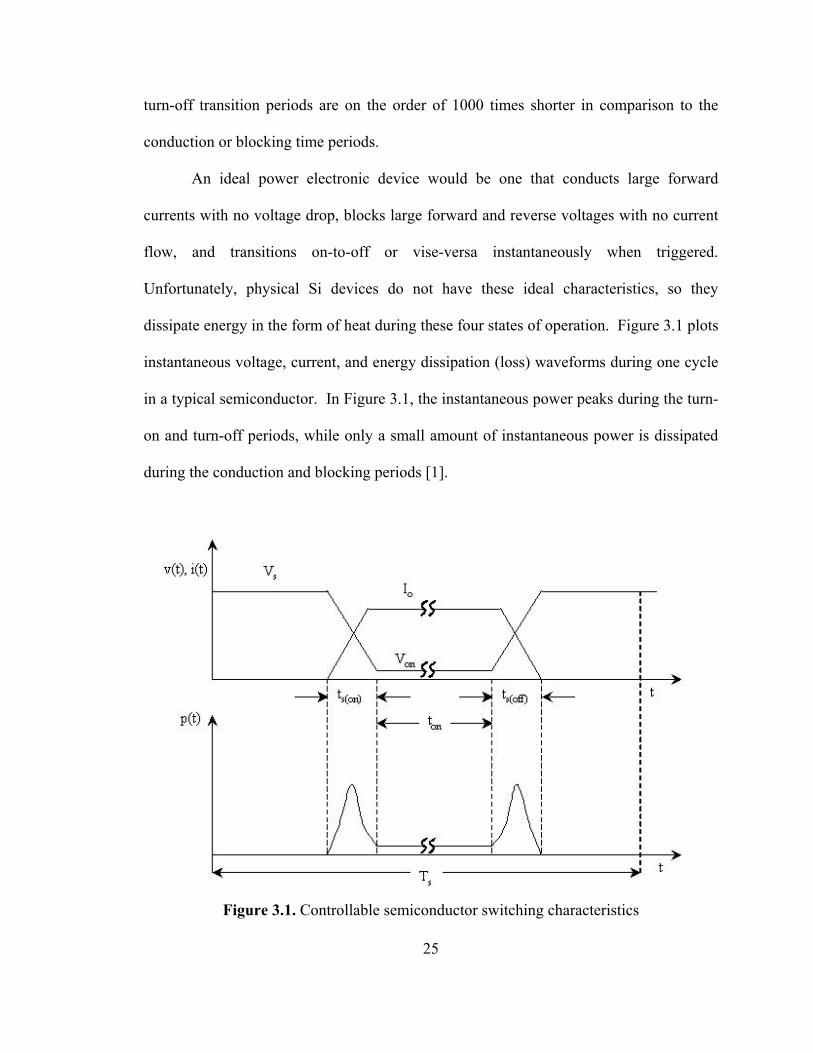
turn-off transition periods are on the order of 1000 times shorter in comparison to the
conduction or blocking time periods.
An ideal power electronic device would be one that conducts large forward
currents with no voltage drop, blocks large forward and reverse voltages with no current
flow, and transitions on-to-off or vise-versa instantaneously when triggered.
Unfortunately, physical Si devices do not have these ideal characteristics, so they
dissipate energy in the form of heat during these four states of operation. Figure 3.1 plots
instantaneous voltage, current, and energy dissipation (loss) waveforms during one cycle
in a typical semiconductor. In Figure 3.1, the instantaneous power peaks during the turn-
on and turn-off periods, while only a small amount of instantaneous power is dissipated
during the conduction and blocking periods [1].
Figure 3.1. Controllable semiconductor switching characteristics
25
Total average power dissipation, , in semiconductors during one cycle of
operation can be calculated by (3.1).
avgtP
∫ ⋅= sT
savgt dttitv
TP
0)()(1
(3.1)
where Ts denotes the period of one complete waveform, v(t) is the instantaneous voltage
across the semiconductor, and i(t) is the instantaneous current through the semiconductor.
The equation consists of power dissipated during the four states of operation. Equation
3.1 can be modified to calculate the average power for individual time periods to appear
as (3.2).
∫ ⋅=b
asavg dttitv
TP )()(1 (3.2)
where a and b are the time boundaries for the semiconductor state of operation and Ts,
v(t), and i(t) are the same as (3.1). For example, the average power dissipated during
conduction can be calculated between the interval a equal to t2 and b equal to t3 from
Figure 3.1.
Although the instantaneous power during the turn-on and turn-off periods has the
largest peak value, the time duration is small; therefore, using (3.2), the average power
dissipated is small. Similarly, average power dissipated during block (blocking losses)
are negligible because the leakage current is small. Thus, from (3.2), the average power
dissipated during conduction can dominate the total average power because the time
duration for this period is much larger than the turn-on or turn-off time periods and the
forward current is much greater than in the blocking time period. However, the switching
frequency plays an important role in the calculating the switching losses. The switching
26
frequency can reach a level where the power losses during switching dominate the total
average power dissipated. This is a critical moment for the PE device because without a
properly sized thermal management system, the heat energy is not dissipated quickly
enough and the device will fail.
Because loss, during conduction, is the largest among a semiconductor’s overall
losses, Section 3.1.1 will use a piece-wise linear model method to determine the series
resistance during the conduction time period. This method will be used to verify the
experimental results, and give an accurate representation of the conduction losses
associated with an increase in temperature.
3.1.1 Conduction Losses
A clear representation of the on-state, or conduction, characteristics of a minority
carrier device (diode, BJT, or IGBT) can be determined by the I-V (forward current
versus voltage) curve. From the I-V curve, the on-state voltage drop across the
semiconductor is determined along with the series resistance. A typical diode I-V curve
is shown in Figure 3.2(a), where the curve is modeled based upon (3.3).
⎟⎟
⎠
⎞
⎜⎜
⎝
⎛−=
−
1)(
nkTsIRVq
s eII (3.3)
where Is is the saturation current,
q is the magnitude of electron charge (1.601x10⁻¹⁹C),
k is Boltzmann’s constant (1.3805x10⁻²³ J/K),
T is the temperature in Kelvin,
27
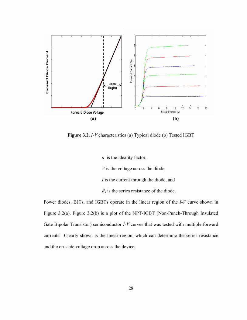
(a) (b)
Figure 3.2. I-V characteristics (a) Typical diode (b) Tested IGBT
n is the ideality factor,
V is the voltage across the diode,
I is the current through the diode, and
Rs is the series resistance of the diode.
Power diodes, BJTs, and IGBTs operate in the linear region of the I-V curve shown in
Figure 3.2(a). Figure 3.2(b) is a plot of the NPT-IGBT (Non-Punch-Through Insulated
Gate Bipolar Transistor) semiconductor I-V curves that was tested with multiple forward
currents. Clearly shown is the linear region, which can determine the series resistance
and the on-state voltage drop across the device.
28
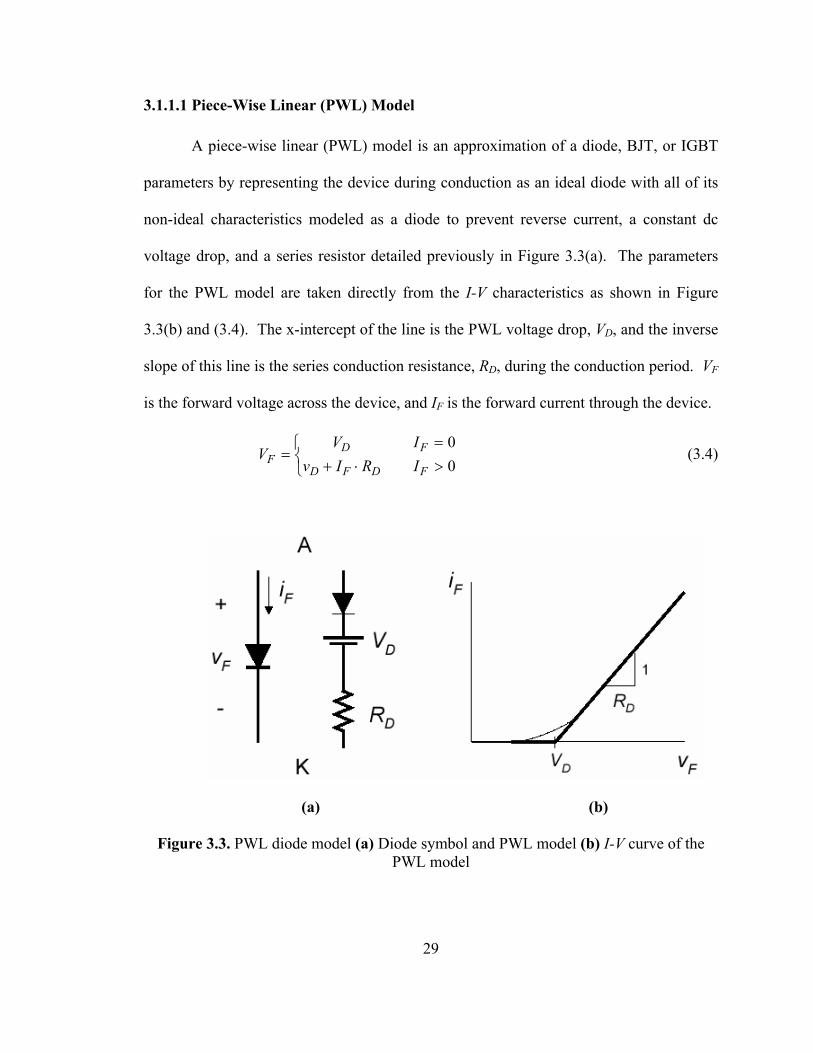
3.1.1.1 Piece-Wise Linear (PWL) Model
A piece-wise linear (PWL) model is an approximation of a diode, BJT, or IGBT
parameters by representing the device during conduction as an ideal diode with all of its
non-ideal characteristics modeled as a diode to prevent reverse current, a constant dc
voltage drop, and a series resistor detailed previously in Figure 3.3(a). The parameters
for the PWL model are taken directly from the I-V characteristics as shown in Figure
3.3(b) and (3.4). The x-intercept of the line is the PWL voltage drop, VD, and the inverse
slope of this line is the series conduction resistance, RD, during the conduction period. VF
is the forward voltage across the device, and IF is the forward current through the device.
00
>=
⎩⎨⎧
⋅+=
F
F
DFD
DF I
IRIv
VV (3.4)
(a) (b)
Figure 3.3. PWL diode model (a) Diode symbol and PWL model (b) I-V curve of the PWL model
29
3.1.1.2 Calculating Conduction Losses
The voltage drop of the device, series resistance, and average and root-mean-
squared values of forward current are the sources of a device’s conduction losses. These
losses can be expressed as:
DrmsDavgcond RIVIP ⋅+⋅= 2 (3.5)
where VD and RD are the PWL parameters found earlier and avgI an rms are the forward
current average and root-mean-squared values.
d I
Equation 3.3 defines forward current as a function of temperature. The tested
IGBT is a minority carrier device with a positive temperature coefficient meaning that as
the temperature increases, so does the series resistance. As the series resistance increases
so do conduction losses, which can cause catastrophic failure if the thermal energy is not
managed within specification. Typically, the junction temperature of Si power devices is
limited to 125 - 150°C, which is also directly proportional to device reliability. As rule
of thumb, the failure rate for semiconductor devices doubles for each 10-15°C
temperature rise above 50°C [1].
3.1.2 PWL Experimental Results
An experimental test was performed to study the effects of junction temperature
on series resistance. The test procedure for determining the temperature characterization
curves for the IGBT were as follows:
30
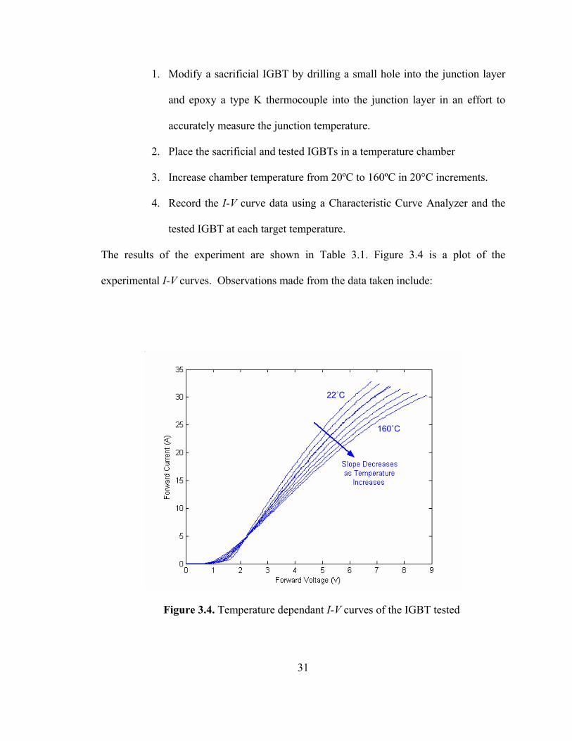
1. Modify a sacrificial IGBT by drilling a small hole into the junction layer
and epoxy a type K thermocouple into the junction layer in an effort to
accurately measure the junction temperature.
2. Place the sacrificial and tested IGBTs in a temperature chamber
3. Increase chamber temperature from 20ºC to 160ºC in 20°C increments.
4. Record the I-V curve data using a Characteristic Curve Analyzer and the
tested IGBT at each target temperature.
The results of the experiment are shown in Table 3.1. Figure 3.4 is a plot of the
experimental I-V curves. Observations made from the data taken include:
22˚C
160˚C
Figure 3.4. Temperature dependant I-V curves of the IGBT tested
31
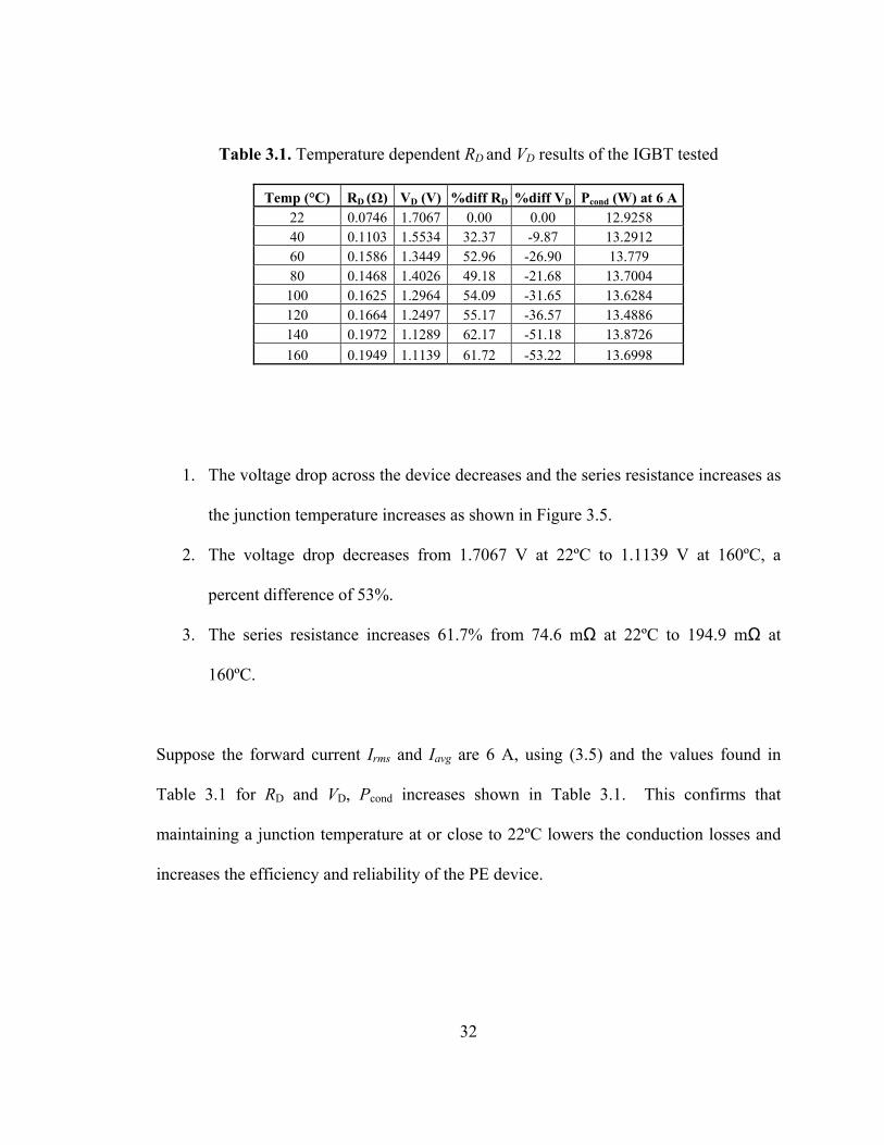
Table 3.1. Temperature dependent RD and VD results of the IGBT tested
Temp (°C) RD (Ω) VD (V) %diff RD %diff VD Pcond (W) at 6 A 22 0.0746 1.7067 0.00 0.00 12.9258 40 0.1103 1.5534 32.37 -9.87 13.2912 60 0.1586 1.3449 52.96 -26.90 13.779 80 0.1468 1.4026 49.18 -21.68 13.7004 100 0.1625 1.2964 54.09 -31.65 13.6284 120 0.1664 1.2497 55.17 -36.57 13.4886 140 0.1972 1.1289 62.17 -51.18 13.8726 160 0.1949 1.1139 61.72 -53.22 13.6998
1. The voltage drop across the device decreases and the series resistance increases as
the junction temperature increases as shown in Figure 3.5.
2. The voltage drop decreases from 1.7067 V at 22ºC to 1.1139 V at 160ºC, a
percent difference of 53%.
3. The series resistance increases 61.7% from 74.6 mΩ at 22ºC to 194.9 mΩ at
160ºC.
Suppose the forward current Irms and Iavg are 6 A, using (3.5) and the values found in
Table 3.1 for RD and VD, Pcond increases shown in Table 3.1. This confirms that
maintaining a junction temperature at or close to 22ºC lowers the conduction losses and
increases the efficiency and reliability of the PE device.
32
R D , Ω
V D ,
V
Temperature °C Temperature °C
(a) (b)
Figure 3.5. PWL model parameters versus temperature (a) RD vs. T (b) VD vs. T
3.1.3 Switching Losses
Diode, BJT, and IGBT switching losses consist of the power dissipated during
turn-on and turn-off time periods. Each of the three devices has minor differences during
the switching process that contribute to differences in switching losses. Diode switching
losses consist of turn-on, turn-off, and reverse recovery losses. The reverse recovery loss
is dominant, while turn-on and turn-off losses are negligible. BJT and IGBT switching
losses consist of turn-on and turn-off losses based on forward current and voltage. IGBT
switching losses are usually smaller than BJT switching losses because of shorter
switching times.
The switching losses for the experimental IGBT can be calculated using (3.2),
where a and b are either t1 and t2 or t3 and t4 from Figure 3.1. The time period between t1
and t2 is the turn-on time ts(on). This is when the voltage across the semiconductor
33
transitions from the blocking voltage, Vs, to the conducting voltage, Von. The converse is
true for the turn-off time ts(off), the time period between t3 and t4. This is when the voltage
across the semiconductor transitions from the conducting voltage, Von, to the blocking
voltage, Vs.
3.2 Experimental Results of Power Dissipation
This section will first present the experimental results of a comparison of the heat
energy dissipated from an IGBT in an air cooled and R134a environments. Second, the
test results from cooling the same IGBT by a mock automotive refrigerant system.
3.2.1 Air Cooled and R134a Cooled Experimental Results
In an effort to determine if R134a is a viable solution to cooling power
electronics, a circuit was constructed and tested in both an air cooled environment and
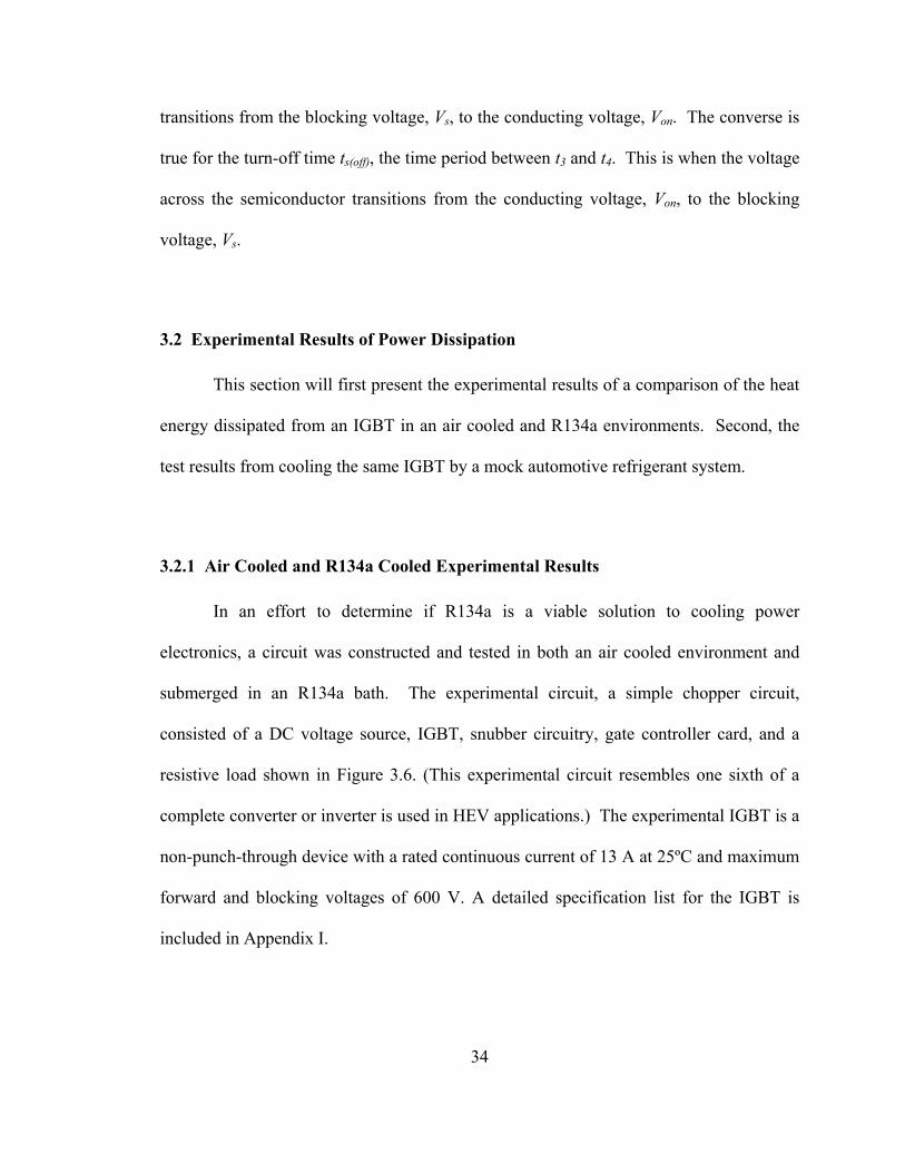
submerged in an R134a bath. The experimental circuit, a simple chopper circuit,
consisted of a DC voltage source, IGBT, snubber circuitry, gate controller card, and a
resistive load shown in Figure 3.6. (This experimental circuit resembles one sixth of a
complete converter or inverter is used in HEV applications.) The experimental IGBT is a
non-punch-through device with a rated continuous current of 13 A at 25ºC and maximum
forward and blocking voltages of 600 V. A detailed specification list for the IGBT is
included in Appendix I.
34
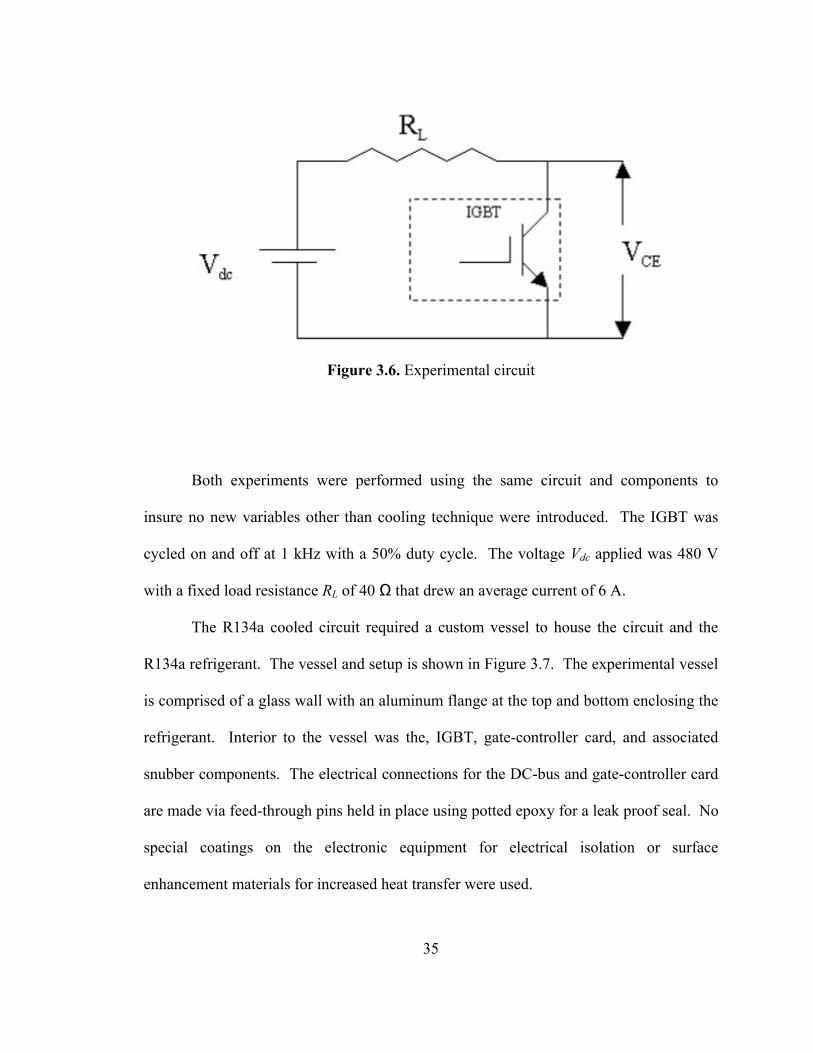
Figure 3.6. Experimental circuit
Both experiments were performed using the same circuit and components to
insure no new variables other than cooling technique were introduced. The IGBT was
cycled on and off at 1 kHz with a 50% duty cycle. The voltage Vdc applied was 480 V
with a fixed load resistance RL of 40 Ω that drew an average current of 6 A.
The R134a cooled circuit required a custom vessel to house the circuit and the
R134a refrigerant. The vessel and setup is shown in Figure 3.7. The experimental vessel
is comprised of a glass wall with an aluminum flange at the top and bottom enclosing the
refrigerant. Interior to the vessel was the, IGBT, gate-controller card, and associated
snubber components. The electrical connections for the DC-bus and gate-controller card
are made via feed-through pins held in place using potted epoxy for a leak proof seal. No
special coatings on the electronic equipment for electrical isolation or surface
enhancement materials for increased heat transfer were used.
35
(a)
(b)
Figure 3.7. Experimental R134a system (a) Submerged IGBT cooling technique (b) Test vessel including PE circuit
36
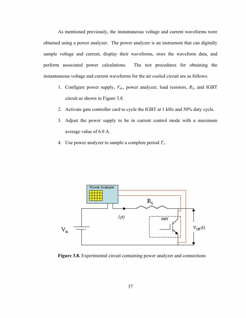
As mentioned previously, the instantaneous voltage and current waveforms were
obtained using a power analyzer. The power analyzer is an instrument that can digitally
sample voltage and current, display their waveforms, store the waveform data, and
perform associated power calculations. The test procedures for obtaining the
instantaneous voltage and current waveforms for the air cooled circuit are as follows:
1. Configure power supply, Vdc, power analyzer, load resistors, RL, and IGBT
circuit as shown in Figure 3.8.
2. Activate gate controller card to cycle the IGBT at 1 kHz and 50% duty cycle.
3. Adjust the power supply to be in current control mode with a maximum
average value of 6.0 A.
4. Use power analyzer to sample a complete period Ts.
Figure 3.8. Experimental circuit containing power analyzer and connections
37
The test procedures for the R134a cooled circuit are the same as for the air cooled
circuit with the exception of enclosing the circuit in the test vessel, pulling the interior of
the test vessel into a vacuum, then filling the vessel with R134a to an appropriate level
where the liquid is slightly above the circuit components.
The IGBT voltage and current waveforms are identical in both air-cooled and
refrigerant-cooled environments. Figures 3.9(a) and (b) are views of voltage and current
transitions for one complete period Ts. Figure 3.9(c) has an expanded view of the voltage
turn-off and current turn-off transitions. Because the waveforms are identical it indicates
that R134a does not change the IGBT turn-on and turn-off periods through the
introduction of additional capacitance across the IGBT terminals or the gate-controller
card. Additional capacitance could slow the IGBTs switching times by momentarily
sustaining a voltage across the gate and source, Vgs, there by increasing switching losses.
Figure 3.9(d) is a plot of instantaneous and average power for both tests. The average
power loss for one complete period Ts of the refrigerant-cooled test was 24.73 W while
the air-cooled test was 22.21 W.
The average power dissipated in Figure 3.9(d) was found using (3.1). Table 3.2
displays the results of average power dissipated from the IGBT in both the air cooled and
R134a cooled environments. The average power for each switching instance of the
switching cycle is found using (3.2).
Mentioned in section 3.1, average conduction losses are the largest power losses
in semiconductors. This idea is shown in Table 3.2, where the average conduction losses
for the experiments are the largest in magnitude among all switching periods. In the air
38
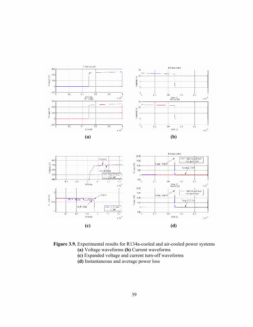
(a) (b)
(c) (d)
Figure 3.9. Experimental results for R134a-cooled and air-cooled power systems
(a) Voltage waveforms (b) Current waveforms (c) Expanded voltage and current turn-off waveforms (d) Instantaneous and average power loss
39
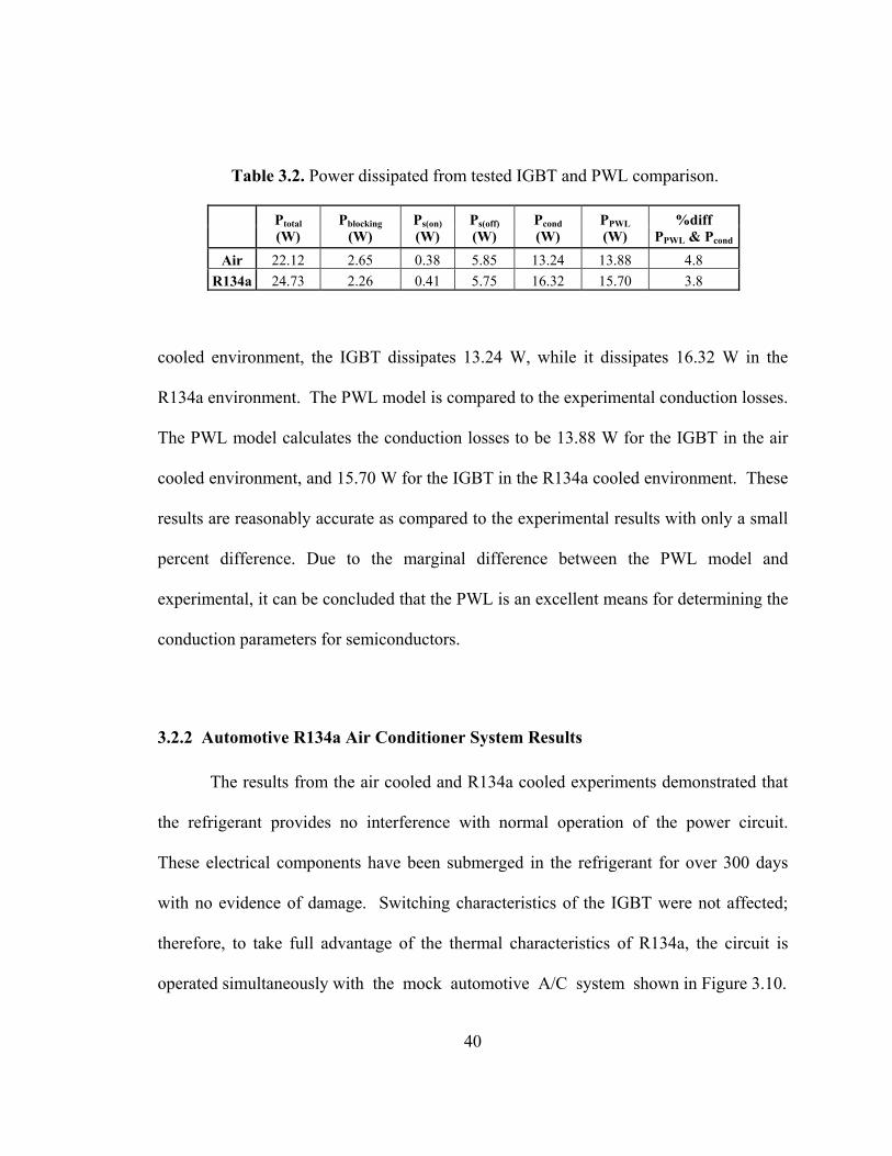
Table 3.2. Power dissipated from tested IGBT and PWL comparison.
Ptotal (W)
Pblocking (W)
Ps(on) (W)
Ps(off) (W)
Pcond (W)
PPWL (W)
%diff PPWL & Pcond
Air 22.12 2.65 0.38 5.85 13.24 13.88 4.8 R134a 24.73 2.26 0.41 5.75 16.32 15.70 3.8
cooled environment, the IGBT dissipates 13.24 W, while it dissipates 16.32 W in the
R134a environment. The PWL model is compared to the experimental conduction losses.
The PWL model calculates the conduction losses to be 13.88 W for the IGBT in the air
cooled environment, and 15.70 W for the IGBT in the R134a cooled environment. These
results are reasonably accurate as compared to the experimental results with only a small
percent difference. Due to the marginal difference between the PWL model and
experimental, it can be concluded that the PWL is an excellent means for determining the
conduction parameters for semiconductors.
3.2.2 Automotive R134a Air Conditioner System Results
The results from the air cooled and R134a cooled experiments demonstrated that
the refrigerant provides no interference with normal operation of the power circuit.
These electrical components have been submerged in the refrigerant for over 300 days
with no evidence of damage. Switching characteristics of the IGBT were not affected;
therefore, to take full advantage of the thermal characteristics of R134a, the circuit is
operated simultaneously with the mock automotive A/C system shown in Figure 3.10.
40
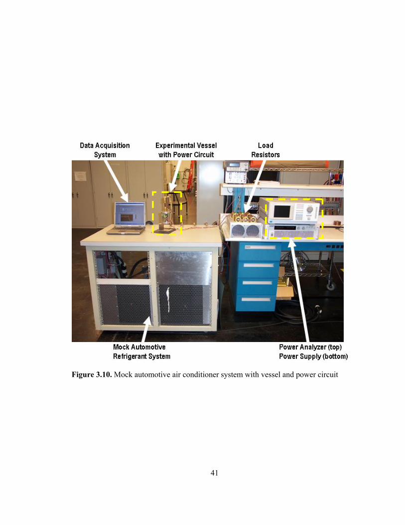
Figure 3.10. Mock automotive air conditioner system with vessel and power circuit
41

The mock automotive A/C system is constructed from components that comprise
a 2003 Buick Park Avenue A/C system, which includes a compressor, condenser,
evaporator, and control system. A 5 hp, three-phase induction motor provides the
compressor with mechanical power. Two service ports are placed in parallel with the
evaporator refrigeration circuit to provide external mounting and operation to the test
vessel. The automotive A/C system has 9320 W of cooling capacity for cooling the
cabin, which should provide plenty of capacity for cooling the IGBT and proven later.
The objective of this experiment is to observe the IGBT case temperature, IGBT
voltage and current waveforms, and air conditioner system behaviors during
simultaneous operation. The procedures were as follows:
1. Enclose experimental IGBT circuit in the test vessel, and connect associated
refrigerant lines to the air conditioner system.
2. Pull a vacuum in the vessel and refrigerant lines.
3. Fill vessel and refrigerant lines to appropriate level.
4. Follow 1 through 4 of air cooled circuit procedure.
5. Activate air conditioner system and open service valves to cycle refrigerant
through the vessel.
6. Monitor the refrigerant liquid level and make necessary adjustments.
7. Turn-on power supply and power analyzer and monitor instantaneous voltage
and current waveforms.
8. Increase current by 1 A in 30 minute intervals from 6 A to 10 A.
The test required temperature acquisition devices to capture, analyze, and record
ambient, IGBT case, and vessel refrigerant temperatures. A LabView program was
42
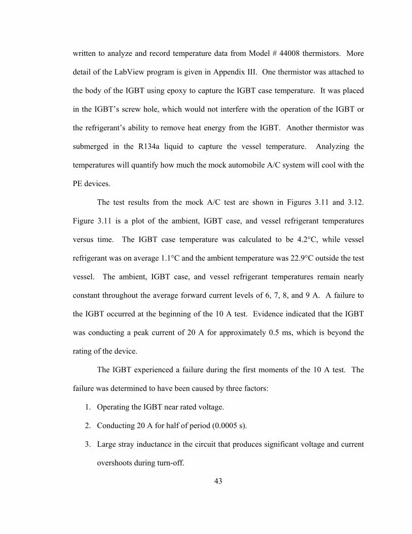
written to analyze and record temperature data from Model # 44008 thermistors. More
detail of the LabView program is given in Appendix III. One thermistor was attached to
the body of the IGBT using epoxy to capture the IGBT case temperature. It was placed
in the IGBT’s screw hole, which would not interfere with the operation of the IGBT or
the refrigerant’s ability to remove heat energy from the IGBT. Another thermistor was
submerged in the R134a liquid to capture the vessel temperature. Analyzing the
temperatures will quantify how much the mock automobile A/C system will cool with the
PE devices.
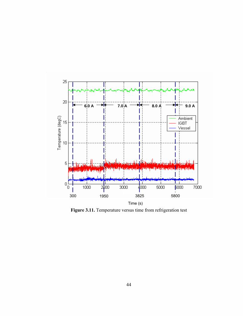
The test results from the mock A/C test are shown in Figures 3.11 and 3.12.
Figure 3.11 is a plot of the ambient, IGBT case, and vessel refrigerant temperatures
versus time. The IGBT case temperature was calculated to be 4.2°C, while vessel
refrigerant was on average 1.1°C and the ambient temperature was 22.9°C outside the test
vessel. The ambient, IGBT case, and vessel refrigerant temperatures remain nearly
constant throughout the average forward current levels of 6, 7, 8, and 9 A. A failure to
the IGBT occurred at the beginning of the 10 A test. Evidence indicated that the IGBT
was conducting a peak current of 20 A for approximately 0.5 ms, which is beyond the
rating of the device.
The IGBT experienced a failure during the first moments of the 10 A test. The
failure was determined to have been caused by three factors:
1. Operating the IGBT near rated voltage.
2. Conducting 20 A for half of period (0.0005 s).
3. Large stray inductance in the circuit that produces significant voltage and current
overshoots during turn-off.
43
9.0 A
300 1950 3825
8.0 A 7.0 A 6.0 A
5800
Time (s)
Figure 3.11. Temperature versus time from refrigeration test
44
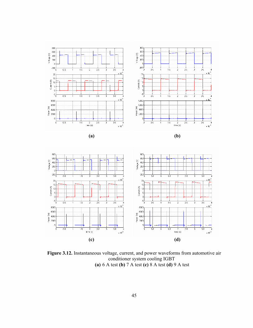
(a) (b)
(c) (d)
Figure 3.12. Instantaneous voltage, current, and power waveforms from automotive air
conditioner system cooling IGBT (a) 6 A test (b) 7 A test (c) 8 A test (d) 9 A test
45
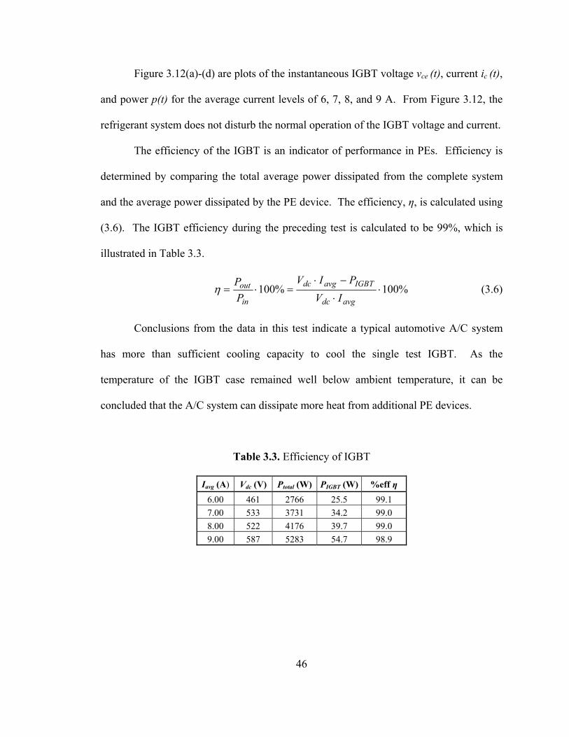
Figure 3.12(a)-(d) are plots of the instantaneous IGBT voltage vce (t), current ic (t),
and power p(t) for the average current levels of 6, 7, 8, and 9 A. From Figure 3.12, the
refrigerant system does not disturb the normal operation of the IGBT voltage and current.
The efficiency of the IGBT is an indicator of performance in PEs. Efficiency is
determined by comparing the total average power dissipated from the complete system
and the average power dissipated by the PE device. The efficiency, η, is calculated using
(3.6). The IGBT efficiency during the preceding test is calculated to be 99%, which is
illustrated in Table 3.3.
%100%100 ⋅⋅
−⋅=⋅=
avgdc
IGBTavgdc
in
outIV
PIVPP
η (3.6)
Conclusions from the data in this test indicate a typical automotive A/C system
has more than sufficient cooling capacity to cool the single test IGBT. As the
temperature of the IGBT case remained well below ambient temperature, it can be
concluded that the A/C system can dissipate more heat from additional PE devices.
Table 3.3. Efficiency of IGBT
Iavg (A) Vdc (V) Ptotal (W) PIGBT (W) %eff η 6.00 461 2766 25.5 99.1 7.00 533 3731 34.2 99.0 8.00 522 4176 39.7 99.0 9.00 587 5283 54.7 98.9
46
3.3 Summary
Silicon (Si) based power electronics devices are based on four states of operation,
which includes conduction, blocking, turn-on, and turn-off. The instantaneous power
dissipated during each state can be calculated using )()( titv ⋅ , where v(t) is the voltage
drop across the device and i(t) is the forward current through the device. A power circuit
containing an IGBT, gate controller card, and snubber was built to study the power
dissipation device and switching characteristics in a PE. An open air and a submerged
test were performed on the circuit to study the switching characteristics of the circuit in
the R134a bath, and the results indicate that the refrigerant offers no alterations to the
circuit. A piece-wise linear (PWL) model was developed using the forward
characteristics of the IGBT, then compared to the average conduction losses found by
. The percent difference for the PWL model was within 5%. And then the
circuit was tested while being cooled by a mock automotive air conditioning system.
Conclusions from the data in this test indicate a typical automotive air conditioner system
has more than sufficient cooling capacity to cool the single test IGBT. As the
temperature of the IGBT case remained well below ambient temperature, it can be
concluded that the air conditioner system can dissipate more heat from additional PE
devices.
)()( titv ⋅
47
Chapter 4
SYSTEMS AND SIMULATION
In the previous chapter, an IGBT circuit was the subject of a series of tests that
provided evidence showing that R134a has good dielectric properties for the voltage and
current range found in HEVs, in addition to having excellent cooling effects on a single
IGBT. This chapter will take the results of chapter 3 and extrapolate the results to a
three-phase, six-IGBT inverter similar to what is found in HEV applications. The
requirements for the inverter are taken directly from the FreedomCAR specifications, and
it will be simulated using custom thin-film resistors in the mock automotive A/C system.
4.1 Three-Phase Inverter From chapter 1, an HEV is propelled via an IC engine and an electric motor.
Electric motors are manufactured in many voltage and horsepower ratings. While many
HEV configurations are possible (series, parallel, hybrid, etc), the common denominator
to all of them is the usage of PEs for the interface and control of the electric motor. The
electric motor of HEVs is typically a three-phase motor because of their convenience in
non-traction applications. The PE package used to control the electric motor is called the
‘inverter’, which is designed to shape and control the three-phase output voltages in
magnitude and frequency. Using an inverter, HEVs can change the on-board battery’s
dc voltage to a three-phase sinusoidal voltage suitable for traction drive motors. A three-
phase inverter consists of three switching legs, one leg per phase, as shown in Figure 4.1.
48
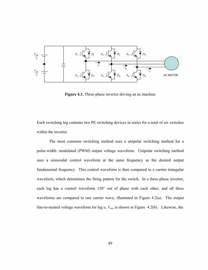
1S
2S
3S1D
2D
3D
4S
5S
6S4D
5D
6D AC MOTOR
aibi
ci
2dcV
2dcV
ab
c
Figure 4.1. Three-phase inverter driving an ac machine
Each switching leg contains two PE switching devices in series for a total of six switches
within the inverter.
The most common switching method uses a unipolar switching method for a
pulse-width- modulated (PWM) output voltage waveform. Unipolar switching method
uses a sinusoidal control waveform at the same frequency as the desired output
fundamental frequency. This control waveform is then compared to a carrier triangular
waveform, which determines the firing pattern for the switch. In a three-phase inverter,
each leg has a control waveform 120° out of phase with each other, and all three
waveforms are compared to one carrier wave, illustrated in Figure 4.2(a). The output
line-to-neutral voltage waveform for leg a, Van, is shown in Figure 4.2(b). Likewise, the
49
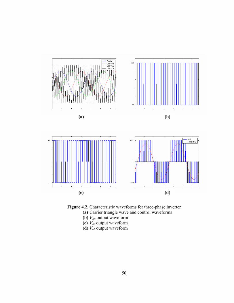
(a) (b)
(c) (d)
Figure 4.2. Characteristic waveforms for three-phase inverter
(a) Carrier triangle wave and control waveforms (b) Van output waveform (c) Vbn output waveform (d) Vab output waveform
50
output voltage waveform for leg b, Vbn, is shown in Figure 4.2(c). The output line-to-line
voltage waveform is found by (4.1) and shown in Figure 4.2(d).
)()()( tVtVtV bnanab −= (4.1)
Mentioned in Chapter 1, the FreedomCAR partners developed a list of design
requirements to be used in the next generation of HEV vehicles. One requirement of the
FreedomCAR is that the electric propulsion system, including inverter, must be capable
of delivering 30 kW of continuous power. The efficiency of the inverter is an important
factor among HEV engineers because it is an indicator of wasted power converted into
heat by the PE devices. The wasted power robs the power from the motor and draws
extra power from the batteries. Efficiency for an inverter is based on many variables
such as semiconductor ratings, switching frequency, supply voltage, phase current, stray
inductance, etc. Typically, an inverter’s efficiency is 96%; therefore, an estimated loss
for a 30 kW inverter is 1200 W continuous.
In the next section, the inverter will be simulated using six thin-film resistors as
the PE devices. Resistors are used because the power loss in an inverter is considered
purely resistive, and an RI 2 loss can model the continuous power loss of each IGBT
during switching. The resistors are cooled by the mock automotive A/C system to
emulate heat from an inverter.
4.2 Thin-Film Resistor
An industry leader in the manufacture of thin-film components, Vishay Electro-
thin-film Films, produced a custom thin-film resistor for the Oak Ridge National
51
Laboratory designed to resemble the footprint of a small PE device. The physical
dimensions of a resistor are 0.51 cm by 0.83 cm by 0.05 cm, and it has a value of 10 Ω.
The manufacturers did not provide any specifications of the resistors; therefore, power
dissipation, current, and temperature limits were unknown.
Our main objective is to test the resistors in a method that best simulates the
power dissipation of an inverter used in an HEV application during normal operation.
From section 4.1, the average power dissipated by the PE devices in the form of waste
heat was estimated to be 1200 W.
Six resistors were configured into a circuit as shown in Figure 4.3. Three parallel
branches of two parallel resistors were placed into the vessel, used and described
previously, and connected to an external dc power supply. The experimental procedures
used to test the power dissipation capabilities of the system were the following:
1. Enclose the resistor circuit in the test vessel, and connect associated
refrigerant lines to the air conditioner system.
2. Pull a vacuum in the vessel and refrigerant lines.
3. Fill vessel and refrigerant lines to appropriate level with refrigerant.
4. Activate air conditioner system and open service valves to cycle refrigerant
through the vessel.
5. Monitor the refrigerant liquid level and make necessary adjustments
6. Turn-on power supply and monitor voltage and current meters.
7. Record the temperatures of each resistor branch and vessel refrigerant.
8. Increase current by 1 A intervals beginning at 16 A after resistor temperatures
reach steady state
52
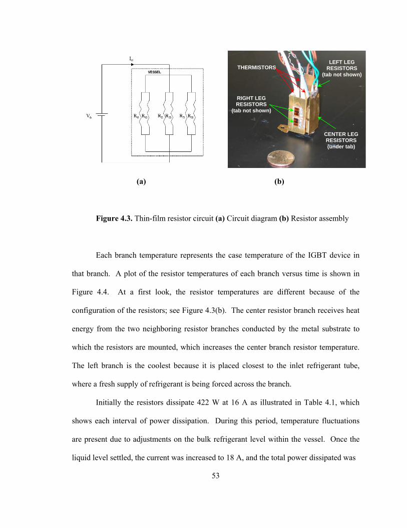
LEFT LEG RESISTORS
(tab not shown)
CENTER LEG RESISTORS (under tab)
RIGHT LEG RESISTORS
(tab not shown)
THERMISTORS
(a) (b)
Figure 4.3. Thin-film resistor circuit (a) Circuit diagram (b) Resistor assembly
Each branch temperature represents the case temperature of the IGBT device in
that branch. A plot of the resistor temperatures of each branch versus time is shown in
Figure 4.4. At a first look, the resistor temperatures are different because of the
configuration of the resistors; see Figure 4.3(b). The center resistor branch receives heat
energy from the two neighboring resistor branches conducted by the metal substrate to
which the resistors are mounted, which increases the center branch resistor temperature.
The left branch is the coolest because it is placed closest to the inlet refrigerant tube,
where a fresh supply of refrigerant is being forced across the branch.
Initially the resistors dissipate 422 W at 16 A as illustrated in Table 4.1, which
shows each interval of power dissipation. During this period, temperature fluctuations
are present due to adjustments on the bulk refrigerant level within the vessel. Once the
liquid level settled, the current was increased to 18 A, and the total power dissipated was
53
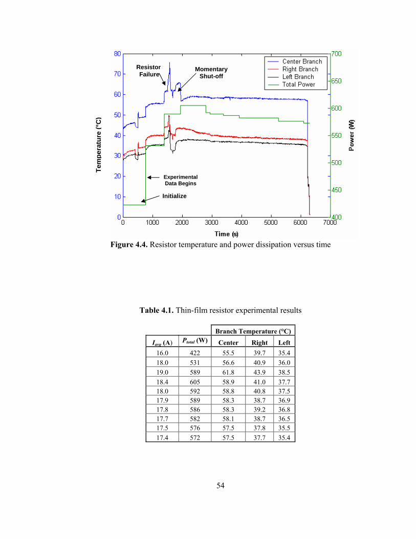
Figure 4.4. Resistor tem
Resistor Failure
Tem
pera
ture
(°C
)
ExperimenData Begi
Initialize
Table 4.1. Thin
Iavg (A) Pto
16.0 18.0 19.0 18.4 18.0 17.9 17.8 17.7 17.5 17.4
Momentary Shut-off
perature and power dissipation versus time
tal ns
-film resistor experimental results
Branch Temperature (°C) tal (W) Center Right Left 422 55.5 39.7 35.4 531 56.6 40.9 36.0 589 61.8 43.9 38.5 605 58.9 41.0 37.7 592 58.8 40.8 37.5 589 58.3 38.7 36.9 586 58.3 39.2 36.8 582 58.1 38.7 36.5 576 57.5 37.8 35.5 572 57.5 37.7 35.4
54
531 W. The center, right, and left branch temperatures reached a steady state temperature
of 55.5°C, 39.7°C, and 35.4°C respectively. The current level was then set to 19 A, and
the total power dissipated was 589 W. After 100 seconds, a portion of the center branch
resistor failed at a temperature of 61.8°C. The center, right, and left branch temperatures
reached a peak of 75.6°C, 49.7°C, and 44.0°C respectively; at which point, the power
supply was deactivated for 80 seconds. A decision was made to continue the experiment
and the power supply was again activated.
Because of the failure, the center branch resistance was altered from 5 Ω to 6.3 Ω;
therefore, more power would be dissipated from the center branch resistors. A decrease
of current from 19.0 A to 18.4 A was set, which resulted in a new power dissipation of
605 W. During this period, the center, right, and left branch temperatures leveled to
59.2°C, 41.5°C, and 37.7°C respectively. Once again, the center resistor begins to fail,
but the power supply was set at a voltage and current limit to prevent a complete failure.
From Figure 4.4, the power dissipated takes a series of decreasing steps because of more
resistor failures until ultimately deactivating the power supply terminated the experiment.
The results of the experiment demonstrate that the automotive air conditioner is
capable of cooling the resistors up to 605 W. The power ratings of the resistors was
unknown, although a reasonable conclusion based upon the experimental results is that if
the resistors have a larger current rating, the automotive A/C could sustain the resistor
temperatures below 120°C at power levels beyond 600 W.
In the next section, the data is extrapolated to determine the temperatures of each
branch resistors and bulk refrigerant temperature while dissipating 1200 W.
55
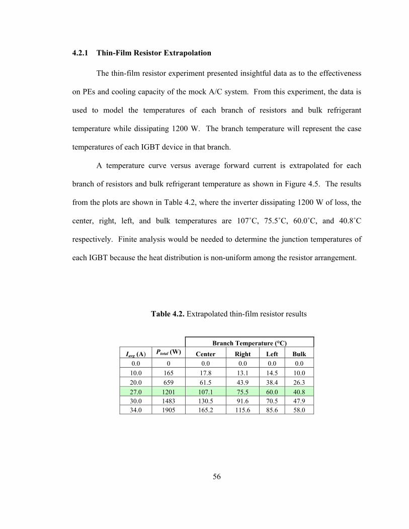
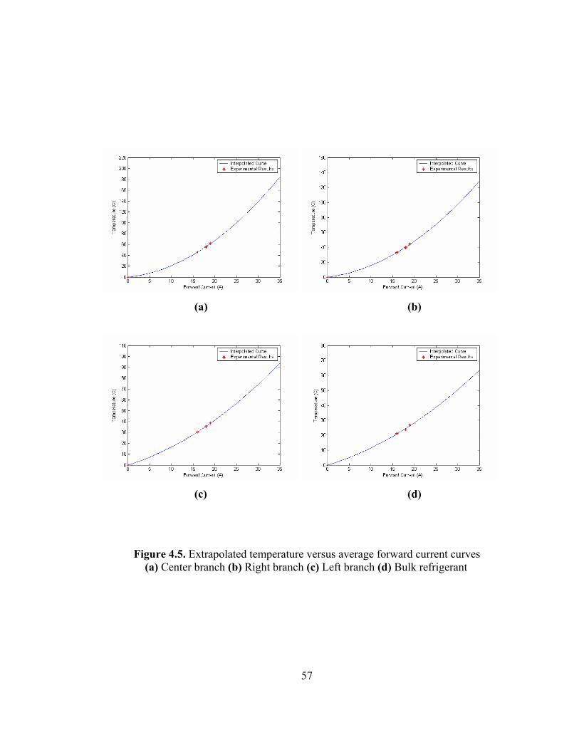
4.2.1 Thin-Film Resistor Extrapolation
The thin-film resistor experiment presented insightful data as to the effectiveness
on PEs and cooling capacity of the mock A/C system. From this experiment, the data is
used to model the temperatures of each branch of resistors and bulk refrigerant
temperature while dissipating 1200 W. The branch temperature will represent the case
temperatures of each IGBT device in that branch.
A temperature curve versus average forward current is extrapolated for each
branch of resistors and bulk refrigerant temperature as shown in Figure 4.5. The results
from the plots are shown in Table 4.2, where the inverter dissipating 1200 W of loss, the
center, right, left, and bulk temperatures are 107˚C, 75.5˚C, 60.0˚C, and 40.8˚C
respectively. Finite analysis would be needed to determine the junction temperatures of
each IGBT because the heat distribution is non-uniform among the resistor arrangement.
Table 4.2. Extrapolated thin-film resistor results
Branch Temperature (°C)
Iavg (A) Ptotal (W) Center Right Left Bulk 0.0 0 0.0 0.0 0.0 0.0
10.0 165 17.8 13.1 14.5 10.0 20.0 659 61.5 43.9 38.4 26.3 27.0 1201 107.1 75.5 60.0 40.8 30.0 1483 130.5 91.6 70.5 47.9 34.0 1905 165.2 115.6 85.6 58.0
56
(a) (b)
(c) (d)
Figure 4.5. Extrapolated temperature versus average forward current curves (a) Center branch (b) Right branch (c) Left branch (d) Bulk refrigerant
57
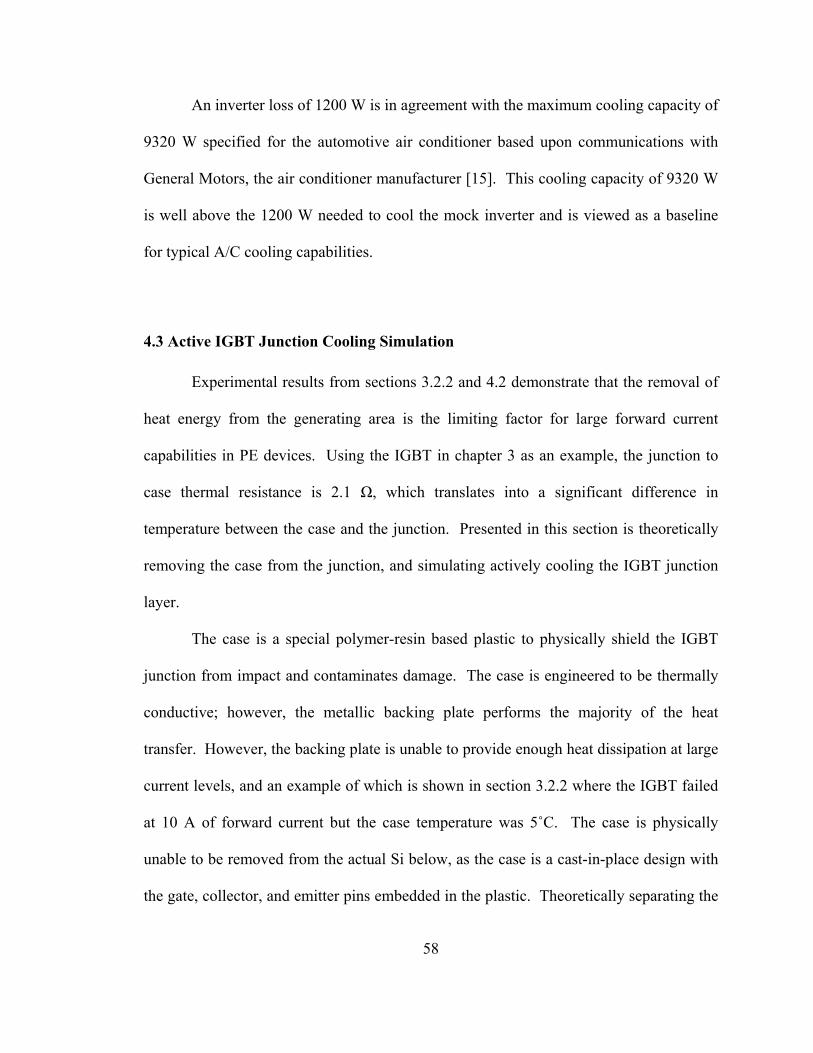
An inverter loss of 1200 W is in agreement with the maximum cooling capacity of
9320 W specified for the automotive air conditioner based upon communications with
General Motors, the air conditioner manufacturer [15]. This cooling capacity of 9320 W
is well above the 1200 W needed to cool the mock inverter and is viewed as a baseline
for typical A/C cooling capabilities.
4.3 Active IGBT Junction Cooling Simulation
Experimental results from sections 3.2.2 and 4.2 demonstrate that the removal of
heat energy from the generating area is the limiting factor for large forward current
capabilities in PE devices. Using the IGBT in chapter 3 as an example, the junction to
case thermal resistance is 2.1 Ω, which translates into a significant difference in
temperature between the case and the junction. Presented in this section is theoretically
removing the case from the junction, and simulating actively cooling the IGBT junction
layer.
The case is a special polymer-resin based plastic to physically shield the IGBT
junction from impact and contaminates damage. The case is engineered to be thermally
conductive; however, the metallic backing plate performs the majority of the heat
transfer. However, the backing plate is unable to provide enough heat dissipation at large
current levels, and an example of which is shown in section 3.2.2 where the IGBT failed
at 10 A of forward current but the case temperature was 5˚C. The case is physically
unable to be removed from the actual Si below, as the case is a cast-in-place design with
the gate, collector, and emitter pins embedded in the plastic. Theoretically separating the
58
case from the junction will be explored where the junction layer will be exposed to the
ambient. Also, the gate, collector, and emitter pins shall be accessible, and a possible
special coating applied only to shield the Si from contaminates. The special coating is
estimated to be a few millionths of an inch applied to the surfaces of the junction layer,
and it shall have a thermal resistance of 0.5 Ω, similar to thermal grease, which is applied
between a PE device and a heat sink to provide even thermal conductivity. The thermal
resistance value was taken from the data sheet for the IGBT found in Appendix I.
4.3.1 Single IGBT Simulation
The junction layer temperature Tj of a single exposed junction IGBT is simulated
and compared to a cased IGBT. The IGBTs are operating under the same switching
frequency, duty cycle, and refrigerant temperature to minimize error. The simulation
incorporates the steady state thermal circuit model of the IGBT and cooling system
described earlier in chapter 2.
The thermal circuit model is shown in Figure 2.1. Equation 2.3 describes the
junction temperature as a function of the thermal resistance between the junction and
ambient, ambient temperature, and average power dissipated by the IGBT. From the
results of the IGBT experiment in section 3.2.2, Figure 4.6 displays the average power
dissipated for the average forward currents of 6, 7, 8, and 9 A. Using quadratic
approximation, the average power dissipated follows (4.2).
322
1 aiaiaP avgavg ++= (4.2)
where: P = Average power dissipated,
59
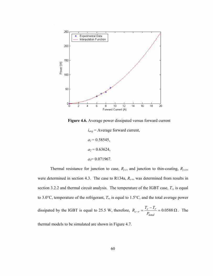
Figure 4.6. Average power dissipated versus forward current
iavg = Average forward current,
a1 = 0.58545,
a2 = 0.63624,
a3= 0.071967.
Thermal resistance for junction to case, Rj-c, and junction to thin-coating, Rj-co,
were determined in section 4.3. The case to R134a, Rc-r, was determined from results in
section 3.2.2 and thermal circuit analysis. The temperature of the IGBT case, Tc, is equal
to 3.0°C, temperature of the refrigerant, Tr, is equal to 1.5°C, and the total average power
dissipated by the IGBT is equal to 25.5 W, therefore, Ω=−
=− 0588.0total
rcrc P
TTR . The
thermal models to be simulated are shown in Figure 4.7.
60
(a) (b)
Figure 4.7. Thermal model (a) IGBT with case (b) IGBT with exposed junction
The simulation will hold constant the switching frequency and duty cycle while
varying the total average power dissipated and forward current. The simulation results
are shown in Figure 4.8, which show that as forward current increases, the junction
temperature increases for both IGBTs. The manufacturer determined the maximum
temperature to be 125°C. The IGBT with the attached case experiences a maximum
junction temperature at 8.5 A; however, the exposed junction IGBT reaches 17.5 A
before meeting the maximum junction temperature. At 17.5 A, the junction temperature
of the IGBT with a case was estimated to be 423°C by simulation.
HEVs would be an ideal application for an inverter built from exposed junction
IGBTs because the inverter would be smaller, lighter, and more reliable than present
designs. Smaller, lighter inverters because the IGBTs they will not have a bulky case.
The IGBTs have a greater current capability; therefore, they will not have to be overrated.
61
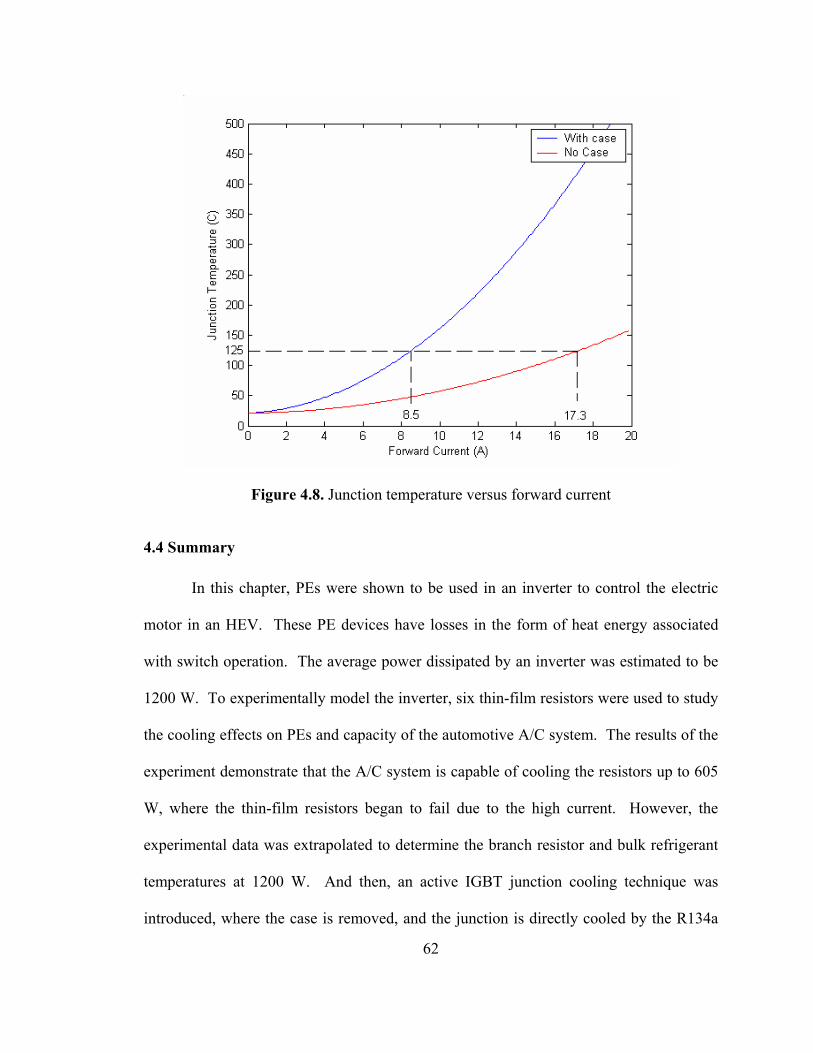
Figure 4.8. Junction temperature versus forward current
4.4 Summary
In this chapter, PEs were shown to be used in an inverter to control the electric
motor in an HEV. These PE devices have losses in the form of heat energy associated
with switch operation. The average power dissipated by an inverter was estimated to be
1200 W. To experimentally model the inverter, six thin-film resistors were used to study
the cooling effects on PEs and capacity of the automotive A/C system. The results of the
experiment demonstrate that the A/C system is capable of cooling the resistors up to 605
W, where the thin-film resistors began to fail due to the high current. However, the
experimental data was extrapolated to determine the branch resistor and bulk refrigerant
temperatures at 1200 W. And then, an active IGBT junction cooling technique was
introduced, where the case is removed, and the junction is directly cooled by the R134a
62

refrigerant. The simulation results show that an IGBT with the attached case experiences
a maximum temperature of 125˚C at 8.5 A; however, the exposed junction IGBT reaches
17.5 A before meeting the maximum junction temperature. This technique maximizes
the effectiveness of the R134a cooling system and the forward current capability of the
PE device.
63
Chapter 5
CONCLUSION AND FUTURE WORK
5.1 Conclusion
Summarizing the contributions of this research endeavor, the chief motivation of
this work was based on finding an alternative to conventional power electronics cooling
methods for hybrid-electric vehicle applications. PEs are vital to the operation and
performance of HEVs because they provide the interface between the energy sources and
the traction drive motor. As with any “real” system, PE devices have losses in the form
of heat energy during normal switching operation, which has the ability to damage or
destroy the device. Thus, to maintain reliability of the PE system, the heat energy
produced must be removed. Present HEV cooling methods provide adequate cooling
effects, but lack sufficient junction temperature control to maintain long-term reliability.
The technique described in this thesis incorporates R134a refrigerant and the on
board air conditioning system to keep PE devices in a reliable range of temperatures.
Proven by experimentation, R134a has no damaging effects on the normal operation for
300 days on a submerged IGBT, gate controller card, and snubber circuits. The IGBT
circuit was operated in an air cooled and R134a environment where the voltage and
current waveforms were compared. Results indicate R134a induces no additional delay
or switching losses for the IGBT circuit. The automotive air conditioner system provided
a constant case temperature of 4.2°C.
64
The automotive air conditioner system was shown to have more than adequate
cooling capacity to cool a six-IGBT inverter. Based on FreedomCAR specifications,
normal operation of the inverter IGBTs will dissipate 600 W of heat energy. The thin-
film resistor experiment proved that the automotive air conditioning could keep the
junction temperature well below the 125°C target.
In addition, experimental data discussed in this thesis proved that the thermal
resistance of the case limits a PE device’s ability to remove heat energy from the junction
layer. A simulated comparson of an IGBT with a case attached and an exposed junction
IGBT was performed using experimental results. The results from the simulation
indicate the exposed junction IGBT technique would benefit by reducing the junction
temperature, increasing forward current ratings, and increase reliability of the device.
Manufacturers of the IGBT would benefit by reducing time of production, materials, and
cost by producing exposed junction IGBTs.
5.2 Future Work
First, future work suggestion begins with R134a refrigerant. The refrigerant was
not intended for cooling power electronics; therefore the actual dielectric properties are
not known. Voltage breakdown characteristics and a multi-year soak study would give a
greater insight to the feasibility of cooling PEs.
Next, study of the effects of enhanced surfaces materials and flow impingement to
assist in the heat transfer process. Enhanced surfaces such as metallic plates with small
(< 0.001 in) ridges scored across the surface. The enhanced surface should assist with the
65
formation and departure of bubbles on the surface, which should increase the efficiency
of the heat transfer of the submerged system. Flow impingement could increase the heat
transfer by direct liquid jetting to the heat source. Flow impingement would ensure a
fresh supply of liquid was in contact with the heat surface.
This thesis only considered steady state conditions, no thermal transients.
Additional study of the thermal transients would help refine thermal model. Thermal
transients are treated as impedances in the circuit diagram rather than pure resistance in
the steady state model. While this is a good approximation, the thermal transients are in
fact the temperature relation of one surface change due to a change in temperature from
another surface. Thermal transients could give greater detail on the junction temperature
as disturbances occur in the circuit.
Last, investigate further the exposed junction IGBT. Simulation has shown that
exposing the junction to the cooling surface greatly reduces the junction temperature.
Actual experimental data would verify the solution and provide additional insight into
methods of heat removal using refrigerant.
66

List of References
67
[1] N. Mohan, T. M. Underland, W. P. Robbins, “Power Electronics, Converters, Applications, and Design,” 3rd ed., John Wiley & Sons, Inc, 2003.
[2] The Merriam-Webster Dictionary, Springfield, Massachusetts, 1997. [3] M. Lugwig, A. Gaedke, O. Slattery, J. Flannery, S. C. O’Mathuna,
“Characterization of Cooling Curves for Power Device Die Attach using a Transient Cooling Curve Measurement,” IEEE Power Electronics Specialists Conference, 2000. PESC 00, Vol. 3, 18-23 June 2000, pp. 1612 – 1617.
[4] I. Mudawar, “Direct-Immersion Cooling for High Power Electronic Chips,”
InterSociety Conference on Thermal Phenomena in Electronics Systems, 5-8 Feb. 1992, pp. 74-84.
[5] R-Theta, “FabFin Product Catalog,” December 1, 1996. [6] D. Faulkner, M. Khotan, R. Shekarriz, “Practical Design of a 1000W/cm2 Cooling
System,” Semiconductor Thermal Measurement and Management Symposium, 11-13 March 2003, pp. 223-230.
[7] M. Saini, R. L. Webb, “Heat Rejection Limits of Air Cooled Plane Fin Heat Sinks
for Computer Cooling,” IEEE Transactions on Computer and Packaging Technologies, Vol. 26, No. 1, March 2003, pp. 71-79.
[8] K. Shenai, “Feasibility and Reliability of High-Temperature Power/Control
Electronics for HEVs,” A technical assessment prepared for Oak Ridge National Laboratories, 12 July 2004.
[9] J. S. Lai, K. Stanton, “Power Electronics Assessment – Vehicle System and
Subsystem Interactions with Power Electronics,” A technical assessment prepared for Oak Ridge National Laboratories, 30 June 2004.
[10] V. A. Sankaran, “Introducing the Power Electronics in Ford Hybrid Escape
Vehicle,” IEEE Power Electronics Society Newsletter, 3rd Quarter 2004, Vol. 16, No. 3, pp. 13-15.
[11] P. E. Phelan, V. A. Chiriac, T. T. Lee, “Current and Future Miniature
Refrigeration Cooling Technologies for High Power Microelectronics,” IEEE Transactions on Component and Packaging Technologies, Vol. 25, No. 3, September 2002, pp. 356-365.
68
[12] P. H. Desai, G. Wiegner, “Evaluation of Freon Modules for Power Electronics Design for a Locomotive Traction Drive,” IEEE Transactions on Industry Applications, Vol. 26, No. 3, May/June 1990, pp. 394-400.
[13] T. Jomard, U. Eckes, E. Touvier, ,M. Lallemand, “Modeling of the Two-Phase
Cooling of a Power Semiconductor and its Associated Evaporators,” Semiconductor Thermal Measurement and Management Symposium, 1992. SEMI-THERM VIII., Eighth Annual IEEE , 3-5 Feb. 1992, pp.20 – 24
[14] C. Tantolin, M. Lallemand, U. Eckes, “Experimental Study of Immersion Cooling
for Power Components,” International Conference on Control, 1994. Vol. 1., 21-24 Mar 1994, pp. 723-727.
[15] G. Major, General Motors, 28 September 2004, personal correspondence.
69

Appendices
70
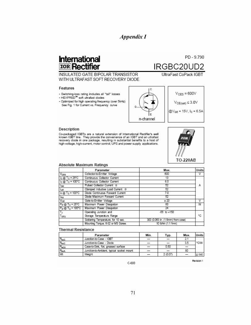
Appendix I
71
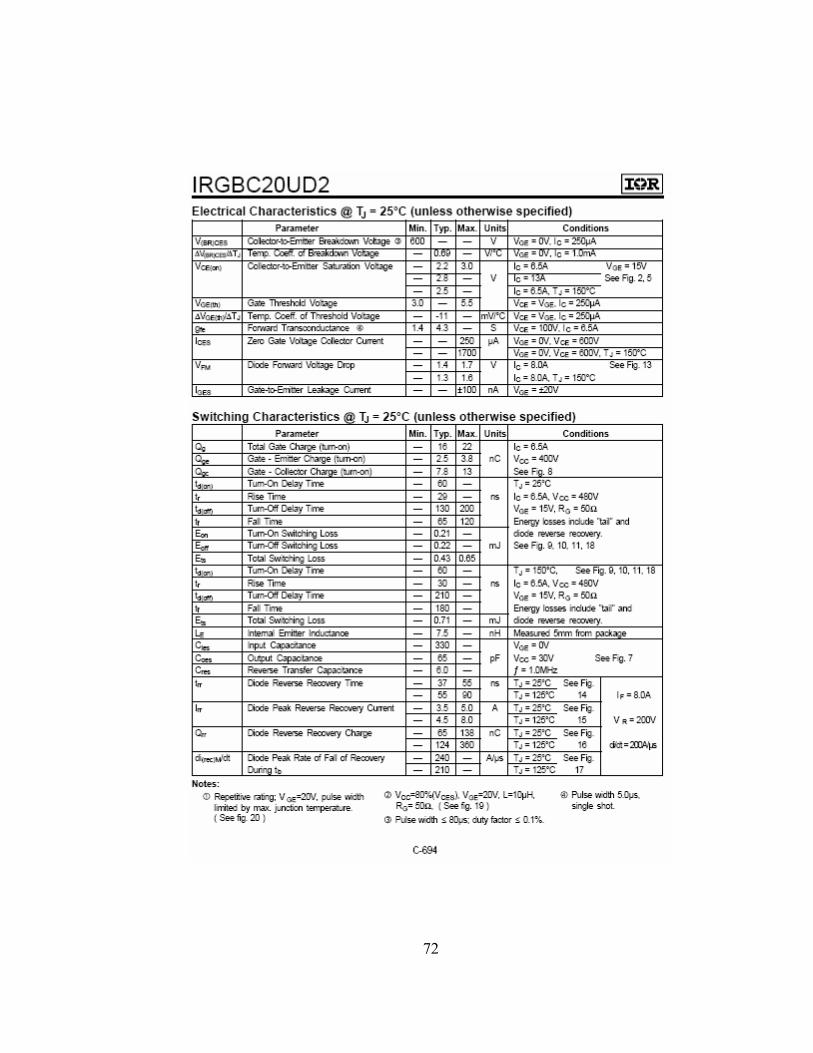
72
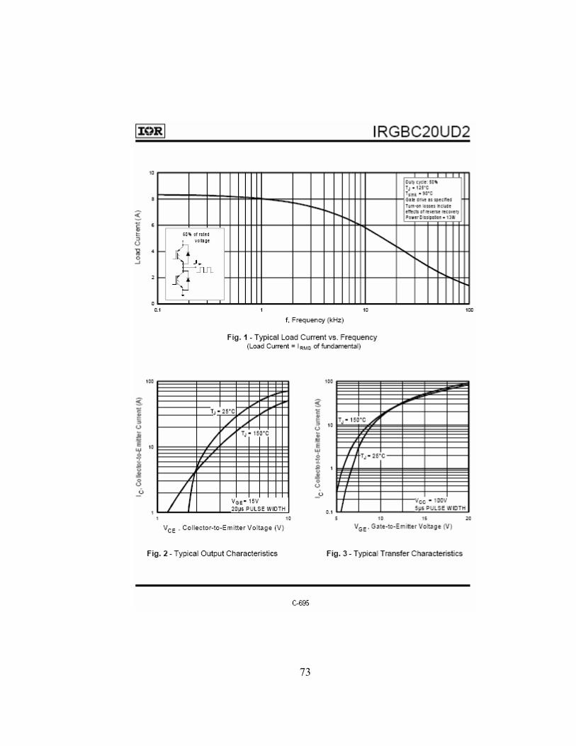
73
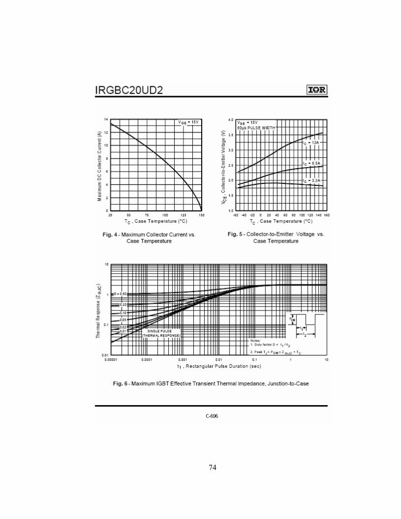
74
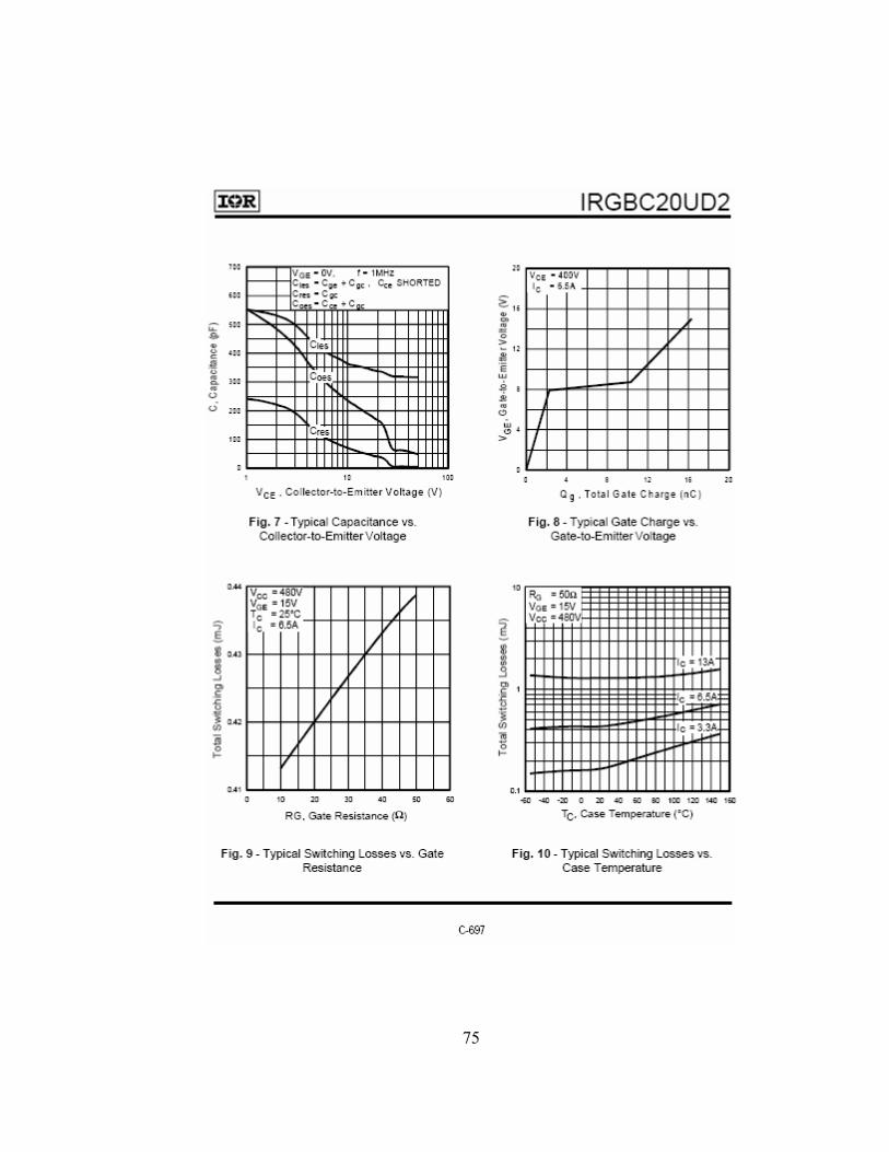
75
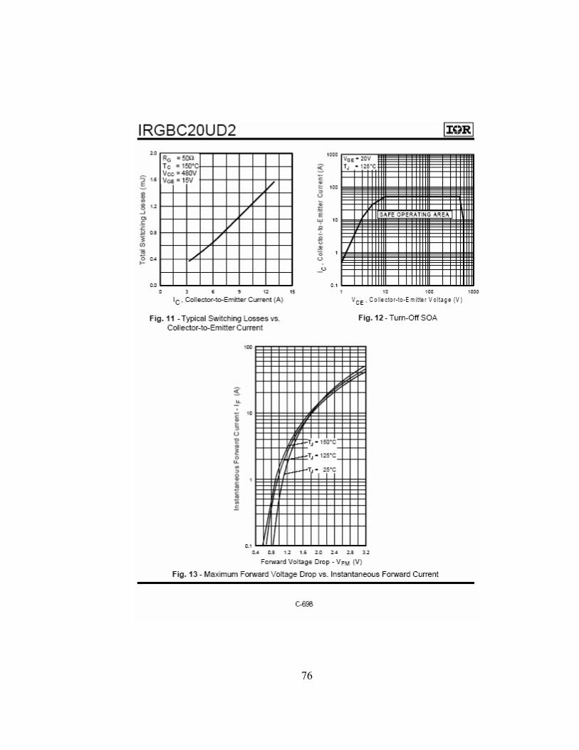
76
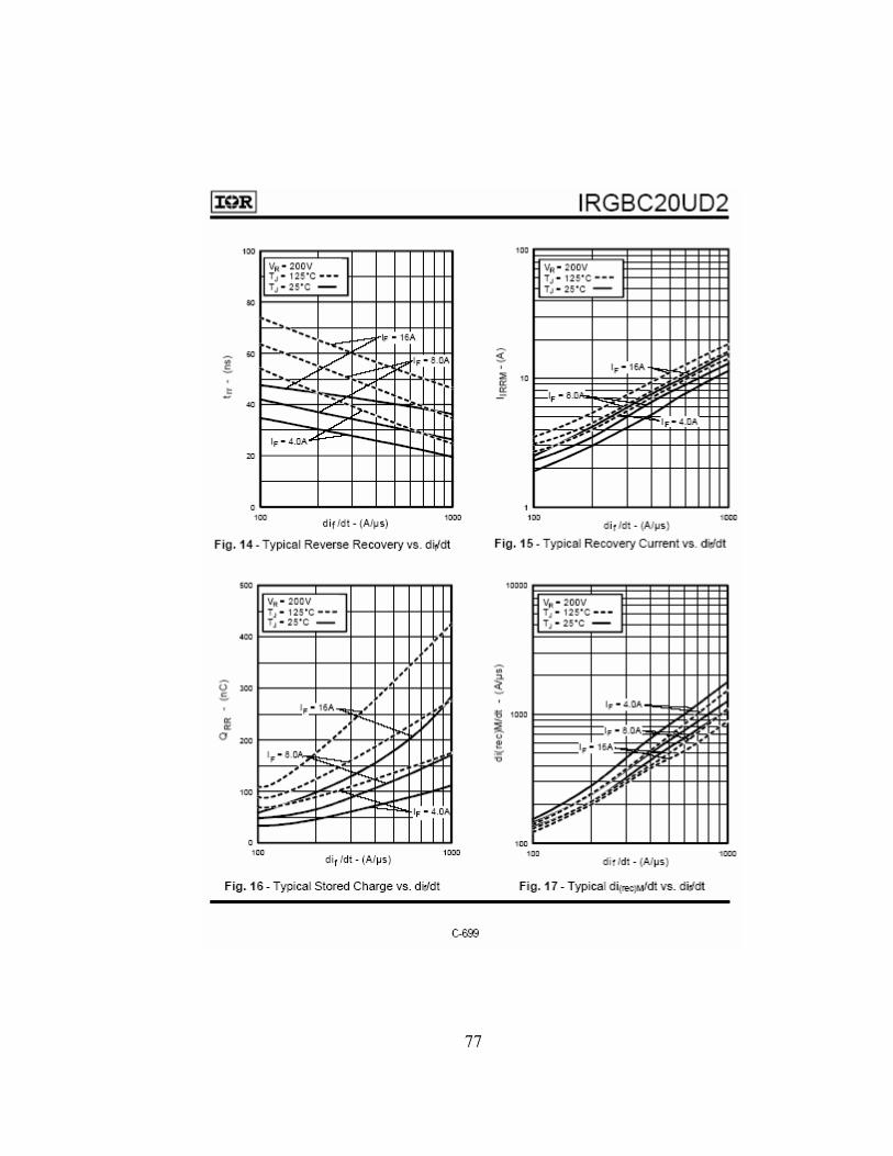
77
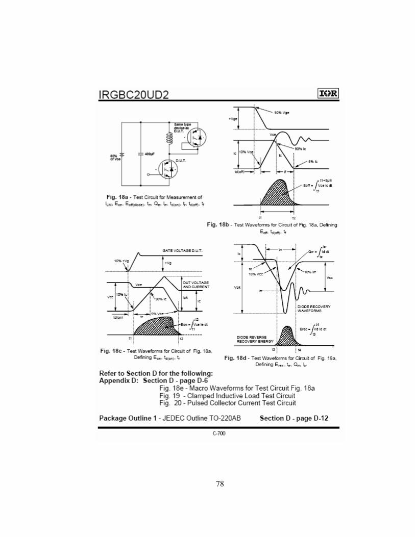
78
Appendix II
List of Equipment 1. International Rectifier, Insulated Gate Bipolar Transistor, Model No.
IRGBC20UD2 2. Dell Latitude D600 notebook computer 3. National Instruments DAQCard 1200, 8 inputs, 2 outputs, 100 kS/s, 12 bit
Multifunction I/O 4. Yokogawa PZ4000 Power Analyzer, DC 2 MHz, 5 MS/s 5. Xantrex DC Power Supply XPR 600-10, 600 V, 10 A 6. Agilent 33250A Function Generator 7. Power Designs, Inc. DC Power Supply, 20.0 V, 1.0 A 8. Dale NH-250 Power Resistor, 250 W, 40 Ω and 80 Ω 9. Vishay Electro-Films, Inc. 10 Ω, Thin-Film Resistors 10. Thermistor Model No. 44008 11. R134a Refrigerant, Dupont 12. 2003 Buick Park Avenue Air Conditioning System comprised of the compressor,
evaporator, condenser, and control system
79
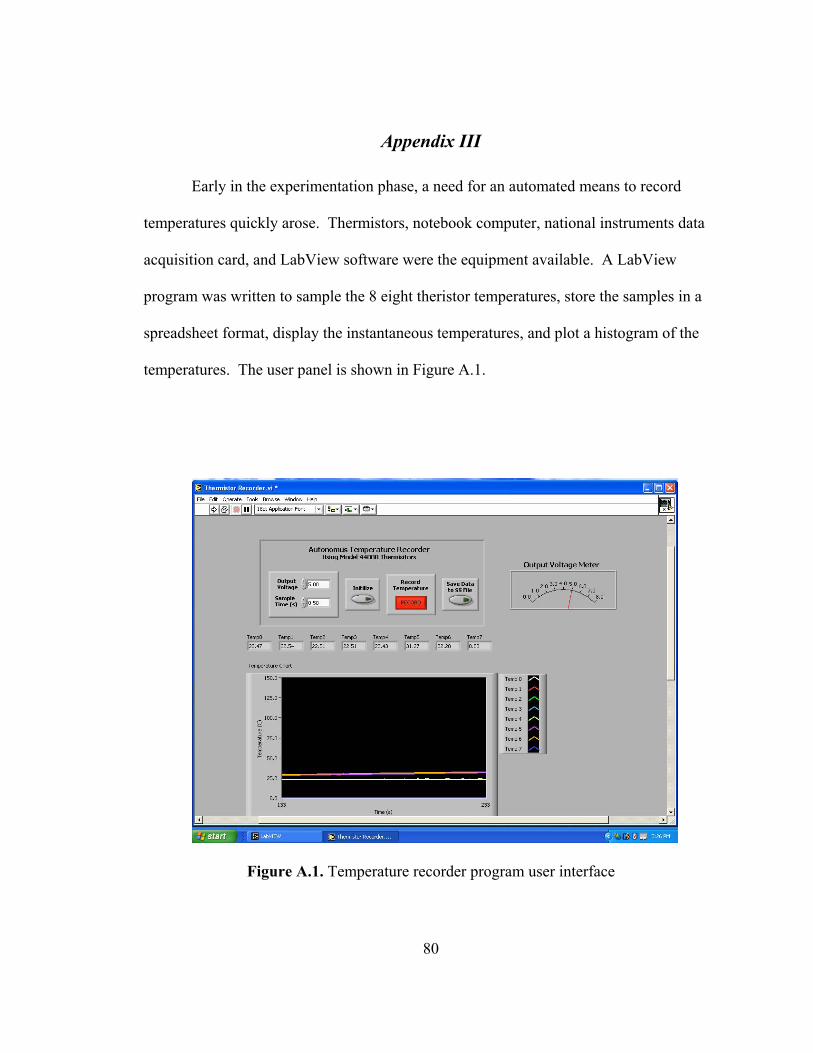
Appendix III
Early in the experimentation phase, a need for an automated means to record
temperatures quickly arose. Thermistors, notebook computer, national instruments data
acquisition card, and LabView software were the equipment available. A LabView
program was written to sample the 8 eight theristor temperatures, store the samples in a
spreadsheet format, display the instantaneous temperatures, and plot a histogram of the
temperatures. The user panel is shown in Figure A.1.
Figure A.1. Temperature recorder program user interface
80
Vita
Jeremy B. Campbell has been actively involved in the study of electricity since
1992 beginning with Industrial Electricity at Fayette Plateau Vocational Center. From
there, he continued his studies of electricity at West Virginia Institute of Technology
from September 1994 to December 1999 graduating with a Bachelors Degree in
Electrical Engineering, while earning a Journeyman’s Electricians Licenses in 1995. He
began his professional career in 2000 for the Department of Defense as a civilian
performing various electrical studies including power systems analysis. During his
graduate studies, Jeremy joined the Post-Graduate Program with the Power Electronics
and Electric Machines Research Center at Oak Ridge National Laboratory, where he
performed research in HEVs including the research contained in this thesis. He plans to
continue his career in the power electronics and power systems industry.
81