Embed Size (px)
Citation preview
A Two Level Power Conversion for High Voltage DC Power Supply for Pulse Load Applications
N.Vishwanathan, Dr. V.Ramanarayanan Power Electronics Group
Dept. of Electrical Engineering, Indian Institute of Science, Bangalore -- 560 012, India.
e-mail: [email protected], e-mail: [email protected] Phone: 091-80-3092932
Keywords DC Power supplies, High frequency power converters, ZVS Converters Abstract High voltage power supply with pulse load (125 KHz and 10 % duty cycle) condition is investigated which is of interest for applications like radar power supplies with output voltage of 22 KV. The performance specifications with this type of power supplies are very stringent demanding tight regulation (< 0.01 %) and high efficiency (> 85%). The solution to this problem as a single stage converter is very difficult. In converters operating at high voltage and high frequency the insulation failure of high voltage transformer is very common. Skin and proximity effect result in higher power losses. Because of high turn’s ratio, the winding capacitance results in delays and large current spikes. Hence a two level converter has been contemplated. One stage of it, namely, Base power supply (BPS), operates at low frequency and produces majority of the output voltage and power. The other one, namely, fast power supply (FPS), operating at high frequency and low output voltage supplies the remaining power and takes care of the transient variations of line and load. The final output voltage is obtained as sum of the outputs of BPS & FPS. The combination of the two stages can satisfy the pulse load specifications. Each of the BPS & FPS use phase modulated-series resonant converter as the power-processing unit with zero voltage switching (ZVS). The analysis of the voltage and power division between BPS & FPS has been done for the proposed topology. It is simulated for a power level of 600 watts and an output voltage of 1 KV as a prototype. It has been studied under various operating conditions of line and load. Simulation results are validated by experimental results.
Introduction High Voltage power supplies find wide range applications as power sources for industrial equipment, medical equipment, air borne applications etc. In many high-power, high-voltage applications such as traveling wave tube (TWT) RF generation, laser based systems for industrial applications (like cutting, marking or surface treatment), X-ray equipment, radar power supplies, there is a requirement for high quality power. In these applications, the power converter may be subjected to either static /slow varying loads or loads with pulsed nature. Radar power supplies are subjected to pulsed loads. Several converters have been proposed in the past to produce and regulate high voltage D.C. Initially they were meant for satellite power supplies [1], [2]. Later these converters were used for other applications. In all high voltage power supplies, the HV transformer is a crucial element. It is due to the large no. of secondary turns and insulation requirements. These two aspects exacerbate the transformer non-idealities, which are winding capacitance and leakage inductance. In all the high-voltage DC-DC power converters, attempt has been made to absorb these non-idealities as useful elements in the power converter topology. It has resulted in series resonant converter (SRC), parallel resonant converter (PRC), series-parallel resonant converter (SPRC) with their own advantages and disadvantages. From the control aspect, two methods are available i.e., variable frequency control and constant frequency phase-modulated control [6], [7], [8]. Phase modulation is generally preferred due
ResonantTank
OutputFilter
LOAD
VDC
HV Trans.
Rect.
S1
S2
S3
S4
L l
w wC Cn2
1:n
Fig.1. Phase-modulated resonant converter Fig.2. Equivalent ckt. of the HV Transformer
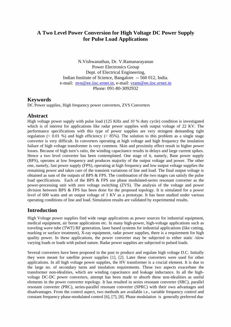
Lr
c r
Lr
cr
Lrcr s
p
cr
(a) series (b) parallel (c) series-parallel Fig.3. Resonant tank circuits to constant switching operation, which yields optimum design of reactive elements. Phase modulated resonant converter is shown in fig.1. The equivalent ckt. of the HV transformer and various resonant tank circuits are shown in fig.2 and fig.3 respectively. In SRC, the series capacitor eliminates the possible saturation of the HV transformer. Capacitive filter at the output is possible. The leakage inductance of the HV transformer is absorbed into the resonant tank ckt. This topology gives high efficiency over a wide range of load variations. The only drawback is that it doesn’t absorb the parasitic winding capacitance into the resonant tank ckt. Though it is a limiting factor, the SRC has been used in the high-voltage, high-power converters due to several other advantages [4]. The PRC absorbs the winding capacitance into the resonant tank ckt. But the PRC requires an LC filter at the output. In high voltage applications, the size of the output filter inductance becomes comparable to the size of the transformer, which is prohibitive. It has been shown in [3] that it is possible to remove this component without degrading the performance of the converter. Even then the PRC has the limitations like, saturation problem of the HV transformer can occur in full bridge topology. Another drawback of PRC is that the current in the resonant components is relatively independent of the load, and efficiency of the converter is relatively low for light loads. The SPRC combines the advantages of the series and parallel converters. The output is controllable for no-load or light-loads, and the light load efficiency is high. In [5], SPRC has been proposed for pulsed load applications. It absorbs all the parasites of the HV transformer. The converter is operated with phase-shifted PWM control at slightly variable frequency. But these converters are complex to analyze and difficult to control.
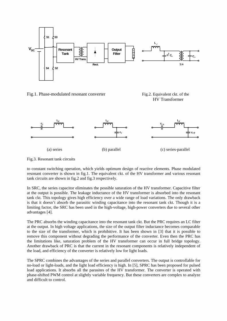
This paper presents a converter topology for high-voltage DC power supplies subjected to pulse loads. Pulse loading exists in applications like radar power supplies with high pulse repetition frequency (PRF). The performance specifications with this type of power supplies are very stringent demanding tight output voltage regulation and high efficiency. Proposed solution is applied to a prototype with the specifications in table-I and fig.4. Actual application requires an output voltage and power level of 22KV and 1.25KW respectively. Table I Supply Voltage: 270VDC±10% Regulation: < 0.01% Output voltage: 1KV Droop: 0.5V/µ sec. Peak Power: 6KW Load Switching Frequency: 125KHz Average Power: 600W Efficiency: > 85%
Load Pulses
OutputVoltage
Time
RegulationDroop
Fig.4 As the load switches at high frequency, if the converter is not regulated properly, the output voltage may collapse totally over a period of time. The converter should switch at-least at twice the load switching frequency for good regulation and stable operation. Tackling high frequency, high voltage, high power and tight regulation in one power converter is a challenging issue. The combination of "high power & high frequency inverter" and "high frequency & high voltage transformer" are critical blocks resulting in number of compromises in terms of output regulation, response time, etc. The problems encountered in general with high voltage and high frequency transformer are: 1) Insulation failure, 2) Skin & proximity effect resulting in increased copper losses and temperature rise, 3) Increased iron losses, 4) Parasites of HV transformer i.e., leakage reactance results in poor regulation and secondary winding capacitance results in current spikes and delay. Hence, the above-mentioned drawbacks lead to the development of a two-level power conversion. In this topology, two power converters are used, each switching at a different frequency. The converter switching at low frequency provides majority of the output voltage and the converter switching at high frequency takes care of the regulation and droop requirements. The division of the power supply helps in overcoming the problems of HV & HF transformer, provides fast response and good regulation without compromising the efficiency constraint.
Phase-Modulated Series Resonant Converter Phase-modulated series resonant converter (PM-SRC) is a very practical approach for the high-voltage DC power supplies. The converter switches at a frequency slightly higher than the resonant frequency of the tank circuit, facilitating ZVS of the devices with the aid of the capacitors connected across them.
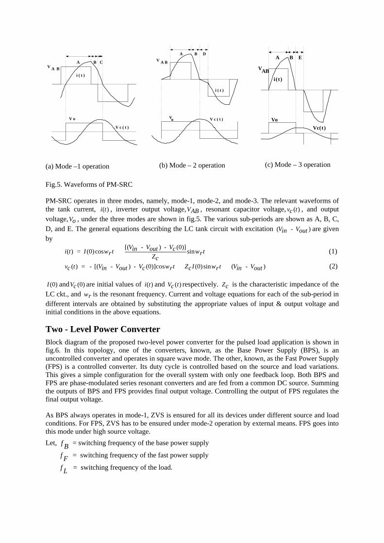
A B CV A B
i ( t )
V c ( t )
V o
(a) Mode –1 operation
A B D
i ( t )
V A B
Vo V c ( t )
(b) Mode – 2 operation
A B E
V c ( t )V o
i ( t )
VA B
(c) Mode – 3 operation
Fig.5. Waveforms of PM-SRC
PM-SRC operates in three modes, namely, mode-1, mode-2, and mode-3. The relevant waveforms of the tank current, ( )i t , inverter output voltage,VAB , resonant capacitor voltage, ( )v tc , and output voltage,Vo , under the three modes are shown in fig.5. The various sub-periods are shown as A, B, C, D, and E. The general equations describing the LC tank circuit with excitation ( - ) V Vin out are given by
[( - ) - (0)]( ) (0)cos sin
V V Vin out ci t I t tr rZcω ω= + (1)
( ) - [( - ) - (0)]cos (0)sin ( - )v t V V V t Z I t V Vc in out c r c r in outω ω= + + (2)
(0)I and (0)Vc are initial values of ( )i t and ( )V tc respectively. Zc is the characteristic impedance of the LC ckt., and rω is the resonant frequency. Current and voltage equations for each of the sub-period in different intervals are obtained by substituting the appropriate values of input & output voltage and initial conditions in the above equations.
Two - Level Power Converter Block diagram of the proposed two-level power converter for the pulsed load application is shown in fig.6. In this topology, one of the converters, known, as the Base Power Supply (BPS), is an uncontrolled converter and operates in square wave mode. The other, known, as the Fast Power Supply (FPS) is a controlled converter. Its duty cycle is controlled based on the source and load variations. This gives a simple configuration for the overall system with only one feedback loop. Both BPS and FPS are phase-modulated series resonant converters and are fed from a common DC source. Summing the outputs of BPS and FPS provides final output voltage. Controlling the output of FPS regulates the final output voltage.
As BPS always operates in mode-1, ZVS is ensured for all its devices under different source and load conditions. For FPS, ZVS has to be ensured under mode-2 operation by external means. FPS goes into this mode under high source voltage.
Let, f B = switching frequency of the base power supply
f F = switching frequency of the fast power supply
f L = switching frequency of the load.
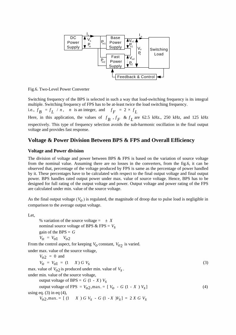
DCPowerSupply
BasePowerSupply
Fast PowerSupply
SwitchingLoad
Feedback & Control
Vs
Is I o
V
V
o1
o2
Vo
Pin1
in2
in
P
P P
P
P
o1
o2
o
Fig.6. Two-Level Power Converter Switching frequency of the BPS is selected in such a way that load-switching frequency is its integral multiple. Switching frequency of FPS has to be at-least twice the load switching frequency. i.e., / f f nB L= , n is an integer, and 2f F = × f L
Here, in this application, the values of , & f f fB F L are 62.5 kHz., 250 kHz, and 125 kHz
respectively. This type of frequency selection avoids the sub-harmonic oscillation in the final output voltage and provides fast response.
Voltage & Power Division Between BPS & FPS and Overall Efficiency
Voltage and Power division
The division of voltage and power between BPS & FPS is based on the variation of source voltage from the nominal value. Assuming there are no losses in the converters, from the fig.6, it can be observed that, percentage of the voltage produced by FPS is same as the percentage of power handled by it. These percentages have to be calculated with respect to the final output voltage and final output power. BPS handles rated output power under max. value of source voltage. Hence, BPS has to be designed for full rating of the output voltage and power. Output voltage and power rating of the FPS are calculated under min. value of the source voltage. As the final output voltage (Vo ) is regulated, the magnitude of droop due to pulse load is negligible in comparison to the average output voltage. Let,
% variation of the source voltage = ± X nominal source voltage of BPS & FPS = Vs gain of the BPS = G
1 2V V Vo o o= + From the control aspect, for keeping Vo constant, 2Vo is varied.
under max. value of the source voltage, 02Vo = and
(1 ) 1V V X G Vo o s= = + (3) max. value of 2Vo is produced under min. value of Vs . under min. value of the source voltage,
output voltage of BPS = (1 - ) G X Vs output voltage of FPS = ,max.2Vo [ - (1 - ) ]V G X Vo s= (4)
using eq. (3) in eq (4), ,max.2Vo [ (1 ) - (1 - ) ] 2 X G V G X V X G Vs s s= + =
2 2 2,max. (1 ) ( 1 )
V X G V Xo sV X G V Xo s
= =+ +
max. power output of FPS 2 ( 1 )
XP Xo
=+
Hence,
max. % of voltage to be produced by FPS = 2
( 1 )XX+
× 100
max. % of power to be handled by FPS = 2
( 1 )XX+
× 100
In the proposed topology, the supply voltage variation is taken as 10%, hence the percentage of voltage and power to be produced by FPS is 18.18%.
Overall Efficiency (η )
1η = efficiency of the BPS
2η = efficiency of the FPS From the fig. (6), the following expressions can be written.
1 2P P P V Iin in in s s= + = (5) 1 2P P Po o o= + (6)
2 2 2 ( ) 1 1 1
P V I Vo o o o K sayP V I Vo o o o
= = =
using eq. (5) and eq. (6), 1 2
1 2
P P Po o oP P Pin in in
η+
= =+
/ 1/ 1// 21 1 11 1 2 1 2 . 1 / 1 / 1 1 1/ (1 )1 1 22 1 2
P PP P o Kin o inP P P P K K ko o oo
η η
η η η
= + = + = + + + + + +
Hence, ( 1 ) 1 2 ( )2 1
K
K
η ηη
η η
+=
+.
Design Considerations
Series Resonant Circuit
As PM-SRC is used in both BPS & FPS, the design of series resonant circuit mainly involves the selection of resonant tank elements ( &L Cr r ) and transformer turns ratio ( n ). For this, all the parameters in the PM-SRC are normalized with respect to the base values. Table II gives the list of the variables and corresponding base values.
Thus the per unit values are VDC = 1.0 p.u, rω = 1.0 p.u, Lr = 1.0 p.u, Cr = 1.0 p.u.
gain of the converter ( M ) = .Vo
nVDC (7)
where Vo = output voltage. The performance of the PM-SRC is dependent on various parameters like tank inductance ( Lr ), tank capacitance ( Cr ), resonant frequency ( rω ), switching frequency ( sω ), load resistance ( RL ), duty
cycle ( D ), and transformer turns ratio ( n ). To take into account the effect of these parameters, these are grouped together as follows:
sr
ωγ
ω= (8)
'
ZcRL
ζ = (9)
where /Z L Cc r r= and '2
RLRLn
=
Table II
Variables Base Values Voltage Input DC Voltage VDC Resistance Tank Char. Impedance, Zc Current /I V ZB DC c= Frequency Resonant frequency, rω Capacitance Cr Inductance Lr
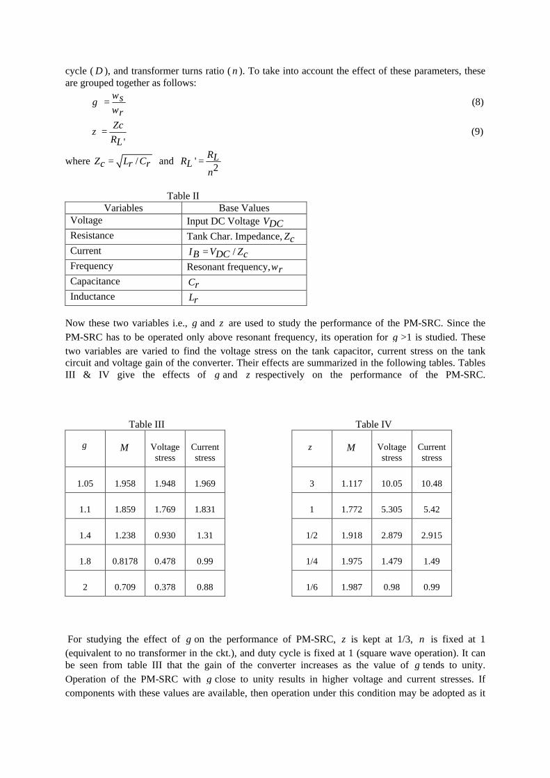
Now these two variables i.e., γ and ζ are used to study the performance of the PM-SRC. Since the PM-SRC has to be operated only above resonant frequency, its operation for γ >1 is studied. These two variables are varied to find the voltage stress on the tank capacitor, current stress on the tank circuit and voltage gain of the converter. Their effects are summarized in the following tables. Tables III & IV give the effects of γ and ζ respectively on the performance of the PM-SRC.
Table III
γ M Voltage stress
Current stress
1.05 1.958 1.948 1.969
1.1 1.859 1.769 1.831
1.4 1.238 0.930 1.31
1.8 0.8178 0.478 0.99
2 0.709 0.378 0.88
Table IV
ζ M Voltage stress
Current stress
3 1.117 10.05 10.48
1 1.772 5.305 5.42
1/2 1.918 2.879 2.915
1/4 1.975 1.479 1.49
1/6 1.987 0.98 0.99
For studying the effect of γ on the performance of PM-SRC, ζ is kept at 1/3, n is fixed at 1 (equivalent to no transformer in the ckt.), and duty cycle is fixed at 1 (square wave operation). It can be seen from table III that the gain of the converter increases as the value of γ tends to unity. Operation of the PM-SRC with γ close to unity results in higher voltage and current stresses. If components with these values are available, then operation under this condition may be adopted as it
results in higher gain of the converter and lower turns ratio of the transformer. Operation under γ = 1 is not preferable as it results in loss of ZVS and SRC will lose inherent short circuit protection. Hence to have all the advantages of higher gain, ZVS, and inherent short circuit protection, operation with γ = 1.05 is selected. Table IV gives the effect of ζ on the operation of PM-SRC. During this study, the values ofγ , D , and n are fixed at 1.05, 1, and 1 respectively. It is observed that as the value of ζ is decreased below unity, the voltage gain is increased while the voltage and current stresses are decreased. Thus the operation of PM-SRC for ζ < 1 is preferred.
Operation of PM-SRC at ζ = 1/6 is preferred as it results in a voltage gain close to 2. It is the max. gain of SRC with voltage doubler at the output. The stresses on tank elements are less than 1 p.u. For BPS, which is operating in a square wave mode with voltage doubler at the output, the design parameters are γ =1.05,ζ = 1/6 and M = 1.987. For FPS, which is also a PM-SRC but operating under variable duty cycle, the design parameters are same as above. But the design is carried out under the condition of min. source voltage and full load. BPS & FPS can be designed using equations (7), (8), (9), selected design parameters, and power ratings of the individual converters. The values of the components obtained are:
For BPS: Lr = 260.08 µ H, Cr = 27.5 nF, n = 1.69
For FPS: Lr = 233.88 µ H, Cr = 1.91 nF, n = 0.38.
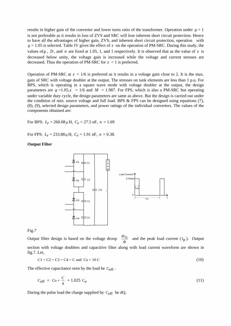
Output Filter
D1
D2
C1
C2
CO
LOAD
D3
D4
C3
C4
6 Amps
t
Load Current
0
Ts
Ton
Fig.7
Output filter design is based on the voltage droop dvodt
and the peak load current ( Ip ). Output
section with voltage doublers and capacitive filter along with load current waveform are shown in fig.7. Let,
C1 = C2 = C3 = C4 = C and Co = 10 C (10)
The effective capacitance seen by the load be Ceff .
Ceff = CCo +
4
= 1.025 Co (11)
During the pulse load the charge supplied by Ceff be dQ.
dQ = Ceff . dvo (12)
also dQ = Ip .Ton = 6 * 0.8 × -610 = 4.8 µ C
dvo = ( 0.5 V/ µ sec ) . ( 0.8 µ sec) = 0.4 V
From equations (10), (11), and (12),
C = 12 µF, C = C = C3 = C4 = 1.17 µF, and C = 11.7 µFeff 1 2 o .
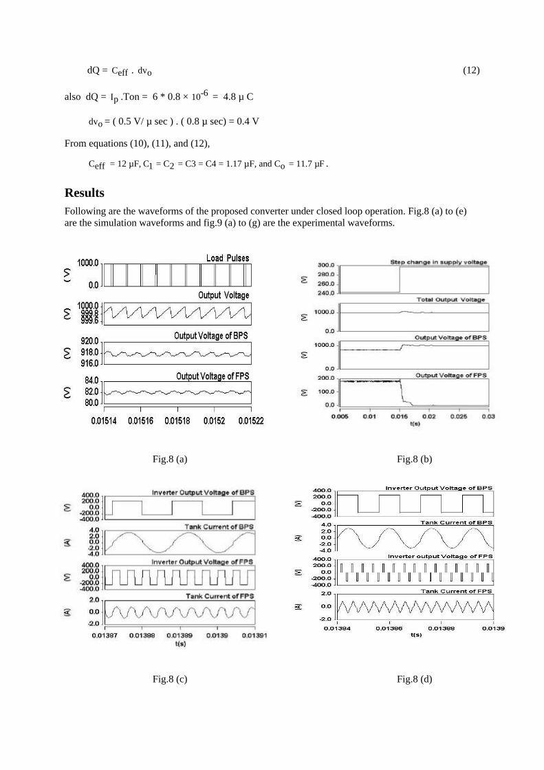
Results Following are the waveforms of the proposed converter under closed loop operation. Fig.8 (a) to (e) are the simulation waveforms and fig.9 (a) to (g) are the experimental waveforms.
Fig.8 (a) Fig.8 (c)
Fig.8 (b) Fig.8 (d)
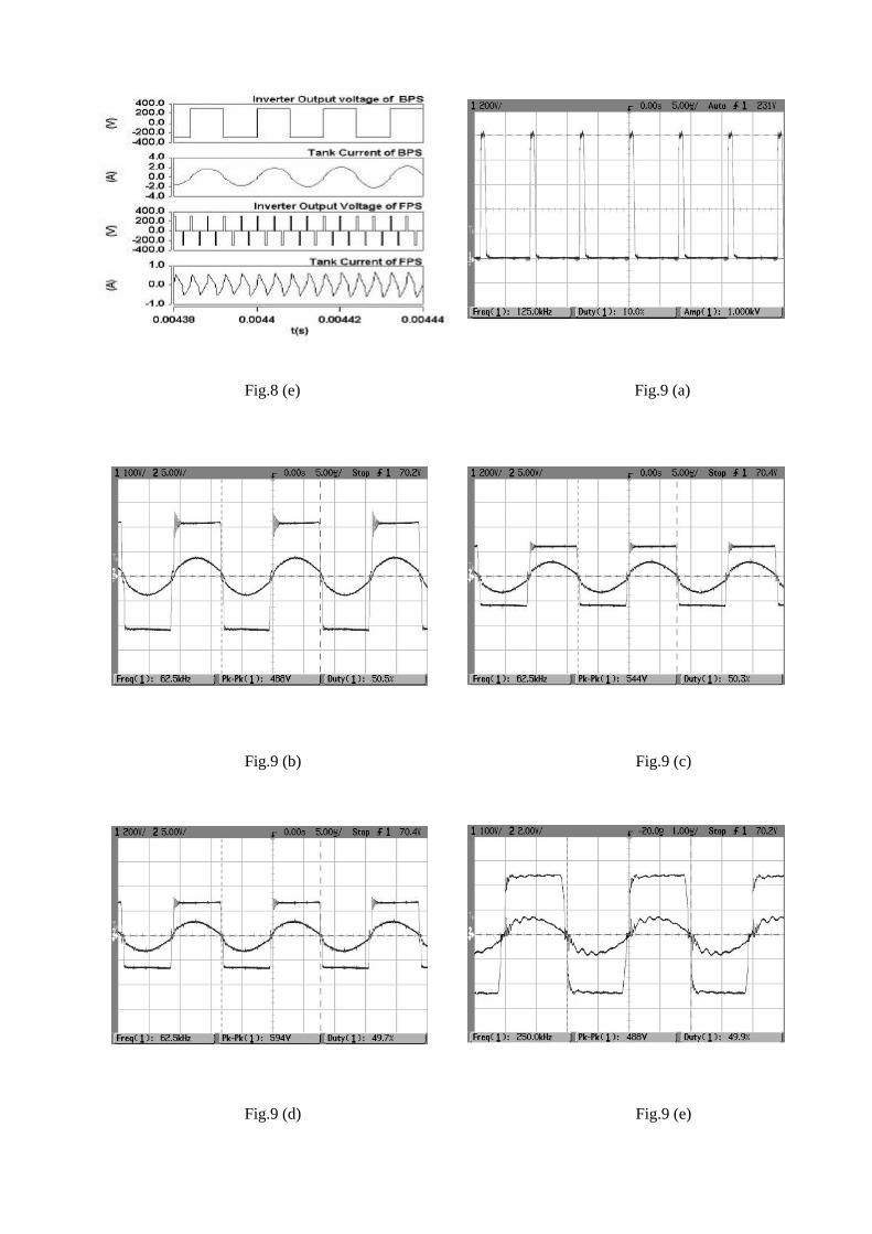
Fig.8 (e) Fig.9 (a) Fig.9 (b) Fig.9 (c) Fig.9 (d) Fig.9 (e)
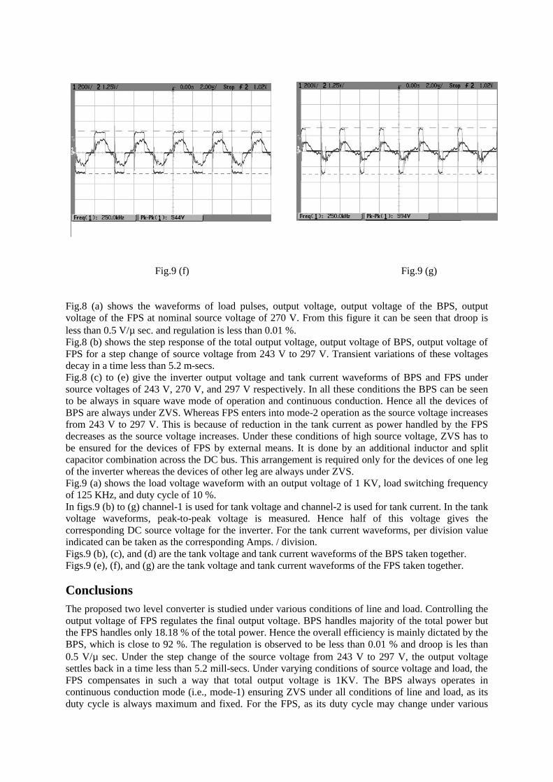
Fig.9 (f) Fig.9 (g) Fig.8 (a) shows the waveforms of load pulses, output voltage, output voltage of the BPS, output voltage of the FPS at nominal source voltage of 270 V. From this figure it can be seen that droop is less than 0.5 V/µ sec. and regulation is less than 0.01 %. Fig.8 (b) shows the step response of the total output voltage, output voltage of BPS, output voltage of FPS for a step change of source voltage from 243 V to 297 V. Transient variations of these voltages decay in a time less than 5.2 m-secs. Fig.8 (c) to (e) give the inverter output voltage and tank current waveforms of BPS and FPS under source voltages of 243 V, 270 V, and 297 V respectively. In all these conditions the BPS can be seen to be always in square wave mode of operation and continuous conduction. Hence all the devices of BPS are always under ZVS. Whereas FPS enters into mode-2 operation as the source voltage increases from 243 V to 297 V. This is because of reduction in the tank current as power handled by the FPS decreases as the source voltage increases. Under these conditions of high source voltage, ZVS has to be ensured for the devices of FPS by external means. It is done by an additional inductor and split capacitor combination across the DC bus. This arrangement is required only for the devices of one leg of the inverter whereas the devices of other leg are always under ZVS. Fig.9 (a) shows the load voltage waveform with an output voltage of 1 KV, load switching frequency of 125 KHz, and duty cycle of 10 %. In figs.9 (b) to (g) channel-1 is used for tank voltage and channel-2 is used for tank current. In the tank voltage waveforms, peak-to-peak voltage is measured. Hence half of this voltage gives the corresponding DC source voltage for the inverter. For the tank current waveforms, per division value indicated can be taken as the corresponding Amps. / division. Figs.9 (b), (c), and (d) are the tank voltage and tank current waveforms of the BPS taken together. Figs.9 (e), (f), and (g) are the tank voltage and tank current waveforms of the FPS taken together.
Conclusions The proposed two level converter is studied under various conditions of line and load. Controlling the output voltage of FPS regulates the final output voltage. BPS handles majority of the total power but the FPS handles only 18.18 % of the total power. Hence the overall efficiency is mainly dictated by the BPS, which is close to 92 %. The regulation is observed to be less than 0.01 % and droop is les than 0.5 V/µ sec. Under the step change of the source voltage from 243 V to 297 V, the output voltage settles back in a time less than 5.2 mill-secs. Under varying conditions of source voltage and load, the FPS compensates in such a way that total output voltage is 1KV. The BPS always operates in continuous conduction mode (i.e., mode-1) ensuring ZVS under all conditions of line and load, as its duty cycle is always maximum and fixed. For the FPS, as its duty cycle may change under various
operating conditions, the range of ZVS is extended by external means. Finally the BPS and FPS put together give an efficiency > 85 % and satisfy all the performance specifications. Experimental results are found to tally with the simulation results.
References [1] Rostad, A.S., Mc Cown, C.T., and Lawrence, D.O. : Application of the venable Converter to a series of satellite TWT power processors, IEEE – PESC,1976, pp.104 – 111. [2] Israelsen, B.P., Martin, J.R., Reeve, C.R., and scown, V.S. : A 2.5 KV high-reliability TWT power supply: Design techniques for high efficiency and low ripple, IEEE – PESC, 1977, pp.212 – 222. [3] Johnson, S.D., Witulski, A.F., Erickson, R.W. : Comparison of resonant topologies in high voltage DC
applications, IEEE Trans. on Aero. and Elect. Systems, vol.24,No.3, May 1988, pp. 263 – 274. [4] Cheron, Y., Foch, H., and Salesses, J. : Study of a resonant converter using power transistor in a 25 KW X – ray tube power supply, IEEE – PESC, 1985, pp. 295 – 306. [5] Garcia, V., Rico, M., Sebastian, J., Hernando, M.M., and Uceda, J. : An optimized DC to DC converter
topology for high voltage pulse load applications, IEEE – PESC, 1994, pp. 1413 – 1421. [6] Pitel, I.J. : Phase modulated resonant power conversion techniques for high frequency inverters, IEEE
Trans. on Ind. Appl. Vol. 22, 1986, pp.1044 – 1051. [7] Tsai, F.S., and Lee, F.C. : Constant frequency, phase controlled resonant power processors, Proc.
IEEE, IAS Annual meeting , 1986, pp. 617 - 622. [8] Ngo, K.D.T. : Analysis of a series resonant converter pulse - width - modulated or current – controlled
for low switching loss, IEEE Trans. on Power Electronics, vol.3, No.1 Jan., 1988, pp. 55 – 63.