Embed Size (px)
Citation preview
Viswam Nathan, Roozbeh Jafari
http://jafari.tamu.edu
TEXAS A&M UNIVERSITY
Updated March 2017
A TUTORIAL ON MOBILE EMBEDDED SYSTEMS
A Tutorial on Mobile Embedded Systems
1 Courtesy of Embedded Signal Processing Lab
http://jafari.tamu.edu
Table of Contents
Getting Started with a Microcontroller .................................................................................................... 2
Microcontroller ....................................................................................................................................... 5
General Description ............................................................................................................................. 5
Instruction Set Architecture (ISA) ......................................................................................................... 6
Clocks .................................................................................................................................................. 7
Low Power Modes ............................................................................................................................... 8
Interrupts ............................................................................................................................................ 8
Timers ............................................................................................................................................... 11
Compare Mode .............................................................................................................................. 11
Capture Mode ............................................................................................................................... 13
Interfacing, IO and AFE .......................................................................................................................... 17
Digital Input/Output (GPIO) ............................................................................................................... 17
Analog Input (AFE) ............................................................................................................................. 18
Analog Output (DAC) ......................................................................................................................... 20
Communication ..................................................................................................................................... 20
Synchronous Communication ............................................................................................................ 20
Serial Peripheral Interface (SPI) ...................................................................................................... 20
Inter-Integrated Circuit (I2C) ........................................................................................................... 24
Asynchronous Communication .......................................................................................................... 26
Universal Asynchronous Receiver/Transmitter (UART) Protocol ..................................................... 26
Data Transmission and Storage .............................................................................................................. 28
Transmission to External Device ........................................................................................................ 28
Bluetooth Serial Link .......................................................................................................................... 28
Data Storage ...................................................................................................................................... 30
Appendix: Useful Resources .................................................................................................................. 33
A Tutorial on Mobile Embedded Systems
2 Courtesy of Embedded Signal Processing Lab
http://jafari.tamu.edu
Getting Started with a Microcontroller This tutorial document is meant to be a primer for working with microcontrollers to realize some simple
applications based on this versatile embedded system. The subsequent sections of the document will go
over the necessary theoretical background and concepts. However, in this section, we describe how to
practically get started using one of these devices. The reason we do this first is to allow the reader to be
able to try out the various example programs found in the document, and also to motivate the reader to
continually program a microcontroller and try out new concepts as and when they are learned through
progression in this tutorial.
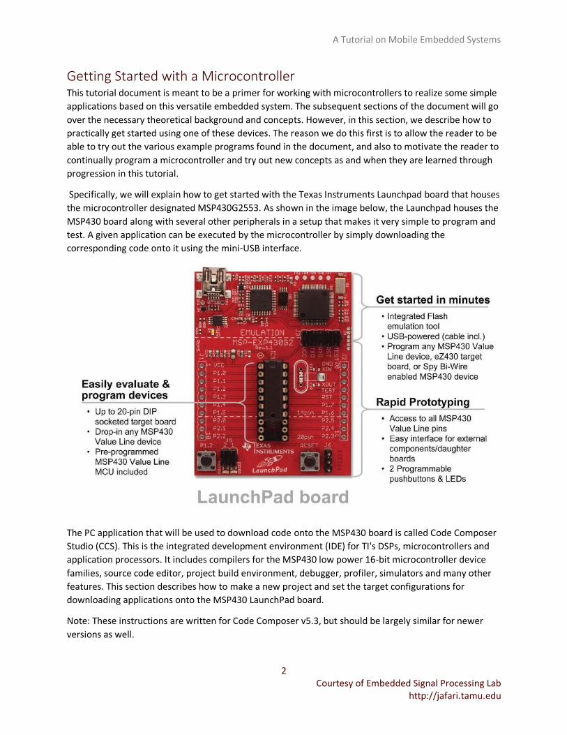
Specifically, we will explain how to get started with the Texas Instruments Launchpad board that houses
the microcontroller designated MSP430G2553. As shown in the image below, the Launchpad houses the
MSP430 board along with several other peripherals in a setup that makes it very simple to program and
test. A given application can be executed by the microcontroller by simply downloading the
corresponding code onto it using the mini-USB interface.
The PC application that will be used to download code onto the MSP430 board is called Code Composer
Studio (CCS). This is the integrated development environment (IDE) for TI's DSPs, microcontrollers and
application processors. It includes compilers for the MSP430 low power 16-bit microcontroller device
families, source code editor, project build environment, debugger, profiler, simulators and many other
features. This section describes how to make a new project and set the target configurations for
downloading applications onto the MSP430 LaunchPad board.
Note: These instructions are written for Code Composer v5.3, but should be largely similar for newer
versions as well.
A Tutorial on Mobile Embedded Systems
3 Courtesy of Embedded Signal Processing Lab
http://jafari.tamu.edu
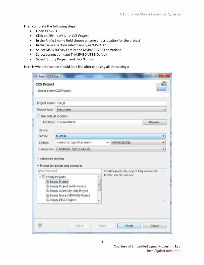
First, complete the following steps:
Open CCSv5.3
Click on File --> New --> CCS Project
In the Project name field choose a name and a location for the project
In the Device section select Family as ‘MSP430’
Select MSP430Gvxx Family and MSP430G2553 as Variant
Select connection type TI MSP430 USB1[Default]
Select ‘Empty Project’ and click ‘Finish’
Here is what the screen should look like after choosing all the settings:
A Tutorial on Mobile Embedded Systems
4 Courtesy of Embedded Signal Processing Lab
http://jafari.tamu.edu
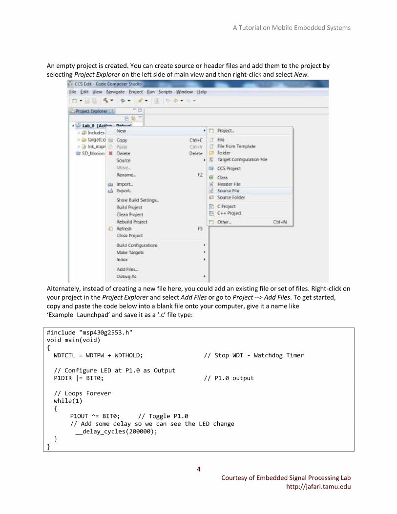
An empty project is created. You can create source or header files and add them to the project by selecting Project Explorer on the left side of main view and then right-click and select New.
Alternately, instead of creating a new file here, you could add an existing file or set of files. Right-click on your project in the Project Explorer and select Add Files or go to Project --> Add Files. To get started, copy and paste the code below into a blank file onto your computer, give it a name like ‘Example_Launchpad’ and save it as a ‘.c’ file type: #include "msp430g2553.h" void main(void) { WDTCTL = WDTPW + WDTHOLD; // Stop WDT - Watchdog Timer // Configure LED at P1.0 as Output P1DIR |= BIT0; // P1.0 output // Loops Forever while(1) { P1OUT ^= BIT0; // Toggle P1.0 // Add some delay so we can see the LED change __delay_cycles(200000); } }
A Tutorial on Mobile Embedded Systems
5 Courtesy of Embedded Signal Processing Lab
http://jafari.tamu.edu
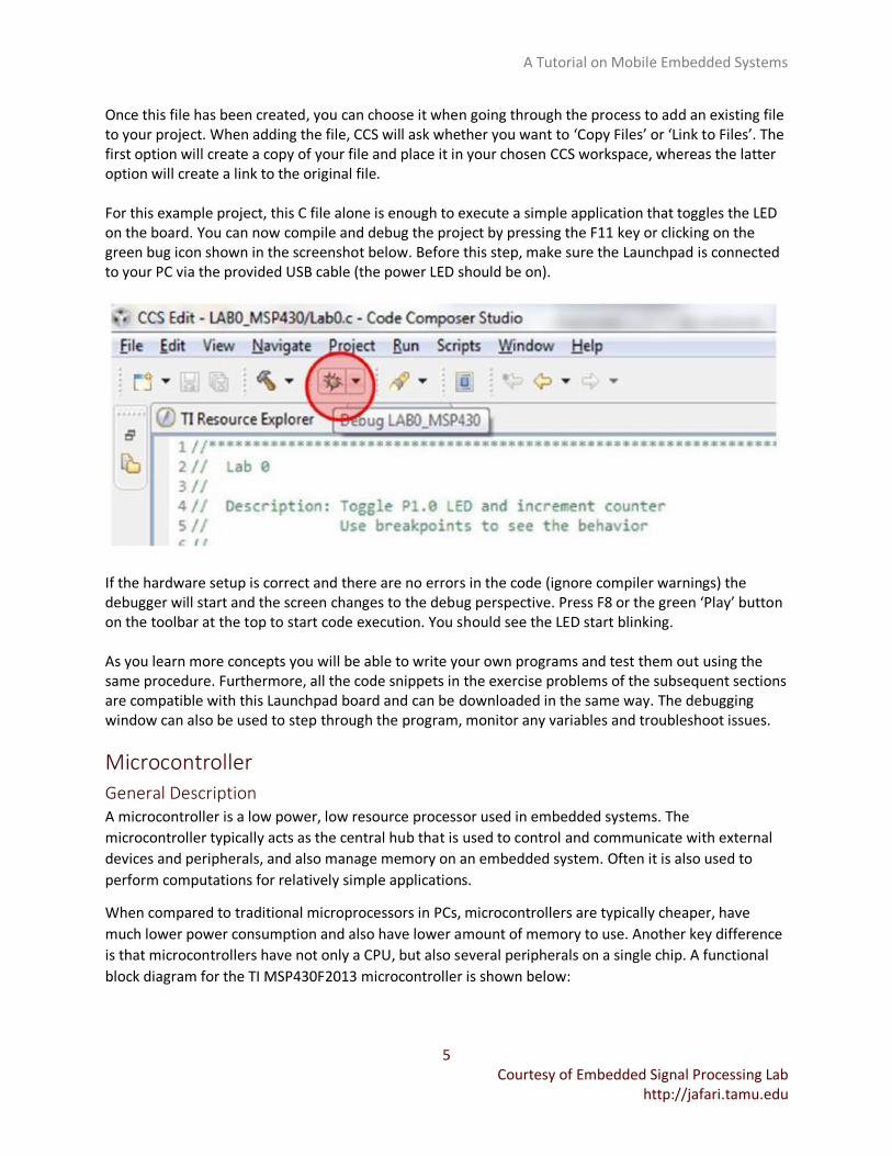
Once this file has been created, you can choose it when going through the process to add an existing file to your project. When adding the file, CCS will ask whether you want to ‘Copy Files’ or ‘Link to Files’. The first option will create a copy of your file and place it in your chosen CCS workspace, whereas the latter option will create a link to the original file. For this example project, this C file alone is enough to execute a simple application that toggles the LED on the board. You can now compile and debug the project by pressing the F11 key or clicking on the green bug icon shown in the screenshot below. Before this step, make sure the Launchpad is connected to your PC via the provided USB cable (the power LED should be on).
If the hardware setup is correct and there are no errors in the code (ignore compiler warnings) the debugger will start and the screen changes to the debug perspective. Press F8 or the green ‘Play’ button on the toolbar at the top to start code execution. You should see the LED start blinking. As you learn more concepts you will be able to write your own programs and test them out using the same procedure. Furthermore, all the code snippets in the exercise problems of the subsequent sections are compatible with this Launchpad board and can be downloaded in the same way. The debugging window can also be used to step through the program, monitor any variables and troubleshoot issues.
Microcontroller
General Description A microcontroller is a low power, low resource processor used in embedded systems. The
microcontroller typically acts as the central hub that is used to control and communicate with external
devices and peripherals, and also manage memory on an embedded system. Often it is also used to
perform computations for relatively simple applications.
When compared to traditional microprocessors in PCs, microcontrollers are typically cheaper, have
much lower power consumption and also have lower amount of memory to use. Another key difference
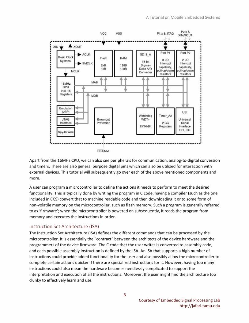
is that microcontrollers have not only a CPU, but also several peripherals on a single chip. A functional
block diagram for the TI MSP430F2013 microcontroller is shown below:
A Tutorial on Mobile Embedded Systems
6 Courtesy of Embedded Signal Processing Lab
http://jafari.tamu.edu
Apart from the 16MHz CPU, we can also see peripherals for communication, analog-to-digital conversion
and timers. There are also general purpose digital pins which can also be utilized for interaction with
external devices. This tutorial will subsequently go over each of the above mentioned components and
more.
A user can program a microcontroller to define the actions it needs to perform to meet the desired
functionality. This is typically done by writing the program in C code, having a compiler (such as the one
included in CCS) convert that to machine readable code and then downloading it onto some form of
non-volatile memory on the microcontroller, such as flash memory. Such a program is generally referred
to as ‘firmware’; when the microcontroller is powered on subsequently, it reads the program from
memory and executes the instructions in order.
Instruction Set Architecture (ISA) The Instruction Set Architecture (ISA) defines the different commands that can be processed by the
microcontroller. It is essentially the “contract” between the architects of the device hardware and the
programmers of the device firmware. The C code that the user writes is converted to assembly code,
and each possible assembly instruction is defined by the ISA. An ISA that supports a high number of
instructions could provide added functionality for the user and also possibly allow the microcontroller to
complete certain actions quicker if there are specialized instructions for it. However, having too many
instructions could also mean the hardware becomes needlessly complicated to support the
interpretation and execution of all the instructions. Moreover, the user might find the architecture too
clunky to effectively learn and use.
A Tutorial on Mobile Embedded Systems
7 Courtesy of Embedded Signal Processing Lab
http://jafari.tamu.edu
The design of the ISA would thus depend on the device and its intended use. Microcontrollers are
typically meant to be lightweight, low power solutions and hence the ISA is relatively small compared to
something like a PC. This dichotomy is borne out by two prominent architecture types: Complex
Instruction Set Computing (CISC) and Reduced Instruction Set Computing (RISC).
CISC, as the name suggests, included complex instructions that encapsulated multiple basic actions. This
led to programs that were shorter and easier to write, but each instruction took longer to execute under
the hood due to the complexity. PCs typically use CISC-like architectures. Microcontrollers on the other
hand, use RISC. RISC consists of simplified, uniform instructions that only completed basic tasks. It led to
longer programs for equivalent tasks, but the time to execute each instruction was lower, the program
flow was more predictable, and the hardware required to support the instruction set was simpler.
The ISA also defines, among other things, the size of individual instructions and the ways in which
memory can be addressed. C is the programming language of choice for most microcontrollers; it is ‘high
level’ enough to be easily readable and usable compared to ‘lower level’ assembly or machine code, and
at the same time it is sufficiently ‘low level’ to allow for efficient coding and use of the device hardware.
Clocks Microcontrollers have one or more clock signals that are used as the basis for any activities that require
timing. The clock signals usually constitute square waves oscillating at a given frequency, and these can
be generated in a few different ways. One popular and intuitive way to generate a regular clock signal is
sourcing an oscillating crystal. This leads to very accurate clock signals with very little error and drift
build-up over time; however the drawback is that this is a relatively expensive solution, both in terms of
monetary cost and power consumption. Another popular alternative is generating a signal using a
custom circuit loop, such as in the case of a digitally controlled oscillator (DCO). This solution is relatively
inexpensive and power-conscious, but is prone to higher rates of error with respect to the true expected
frequency, especially when compared to a corresponding clock signal generated by a crystal. Thus, the
sources of the clock signals have several trade-offs, and care must be taken to choose the right option
taking into account the needs of the application.
In terms of applications, an obvious one for clocks would be the timing of external events and
generation of periodic signals. There are in fact specialized hardware modules to fully utilize the clocks
in this way and these will be described in further detail in the section on ‘Timers’. If we take a more
fundamental look, the execution of code on the microcontroller itself is a synchronous activity; typically
a clock is used to time the execution of successive instructions, with a faster clock resulting in a higher
processing speed but also higher power consumption. Another important application domain for clocks
in the context of microcontrollers is in communication. As we will see in further detail in future sections,
certain types of digital communication require a shared clock between the communicating devices to
synchronize the sending and receiving of data. Finally, these clock signals can also be sent to any
external peripherals that do not have a suitable clock source of their own to function.
In the specific case of the MSP430 microcontroller, there are three clock signals available: the Master
Clock (MCLK), Sub-Main Clock (SMCLK) and the Auxiliary Clock (ACLK). These three signals can be
configured to source their signal from an internal crystal, DCO loop or any other suitable external clock
source. Moreover, there are divider circuits in place so that the clock signal can oscillate at certain
fractions of the given clock source frequency.
A Tutorial on Mobile Embedded Systems
8 Courtesy of Embedded Signal Processing Lab
http://jafari.tamu.edu
The MCLK is used to synchronize the execution of instructions by the central processor and hence
fundamentally defines the timing of the microcontroller’s performance. It can also however, be piped
out and used as a clock signal for other applications in parallel. In general, a higher MCLK speed means
higher performance and more power consumption. The SMCLK and the ACLK can both be used for all of
the other applications of clock signals as mentioned before. The key difference is that the SMCLK
typically supports higher frequencies on the order of MHz, whereas the ACLK is designed to be used for
low frequency clocking applications on the order of a few KHz as necessary.
For more information on the details of the various available clock sources and clock speeds, please refer
to the specific datasheet of the microcontroller. The datasheet for the MSP430G2553 is provided in the
Appendix section at the end of this document.
Low Power Modes One of the key features of an embedded system is energy efficiency, and the microcontroller can help to
save power through customizable low power modes. There are typically multiple levels of low power
modes, with each level increasingly powering down more components of the system to save power. For
example, on the TI MSP430F5438 microcontroller the various power modes, with approximate current
consumption in parentheses, are described as follows:
Active Mode (AM): CPU, all clocks, and enabled modules are active (≈300 μA)
Low Power Mode 0 (LPM0): CPU and MCLK are disabled, SMCLK and ACLK remain active (≈85 μA)
Low Power Mode 3 (LPM3): CPU, MCLK, SMCLK, and DCO are disabled; only ACLK remains active (≈1 μA)
Low Power Mode 4 (LPM4): CPU and all clocks disabled, RAM is retained (≈0.1 μA)
As can be seen, in all low power modes the CPU is disabled so there will be no more computations and
no more code executing. The choice of low power mode depends on which components the user wants
to retain while the CPU is disabled. Low power modes are useful when the system only needs to be fully
active in response to sporadic external events, or if the system only needs to be active for a brief
amount of time in a periodic fashion. In either case the system can be brought back to active mode with
the use of interrupts, which are described in the following section.
Interrupts Interrupts can break the flow of execution of code on a microcontroller to perform a given task in
response to an aperiodic external event or a scheduled internal event. Interrupts are typically high
priority events that require immediate response. For example, if the user presses a button to turn on a
light the system needs to respond immediately to the button press so the user interface remains viable.
The interrupt mechanism enables this by allowing the microcontroller to break out of its current routine,
perform the required actions related to the interrupt, and return back to the previous state to continue
executing the code it was before. Alternatively, interrupts can also work well with low power modes to
reduce energy consumption; for example the device can go into low power mode with no code
executing, and a button press can trigger an interrupt that wakes up the device from low power mode to
perform the required action and then return to sleep if desired. This is in contrast to ‘polling’, wherein
the CPU is fully powered on but is idle waiting for the event to happen. Thus, it is almost always

A Tutorial on Mobile Embedded Systems
9 Courtesy of Embedded Signal Processing Lab
http://jafari.tamu.edu
preferable to use interrupts instead of polling if the CPU is not required to be active while the next event
is pending.
The configurable sources of interrupts can vary, depending on the specific microcontroller and the
hardware available. Some common sources of interrupts include:
1. General Purpose Input/Output (GPIO) pins: These are simply generic digital logic lines that
connect the microcontroller to one or more peripherals. The microcontroller can be configured
such that a transition in logic level triggers an interrupt. For example, the circuit can be designed
in such a way that a button press triggers a logic level ‘1’ on a specific GPIO pin that is
configured for interrupts so that the microcontroller can respond to the button press.
2. Timers: Timers will be described in more detail in the following section, but essentially they are
internal components that can be set up to count to a specific value and trigger an interrupt; this
allows the user to trigger interrupts after known time intervals. They can also be configured to
repeat this process so that the interrupts are periodic.
3. Analog-to-Digital Converter (ADC): The ADC of the microcontroller can trigger an interrupt
when a conversion is complete and the new digitized sample is ready.
Once an interrupt is triggered, the microcontroller begins executing the code in the corresponding
interrupt service routine (ISR). If the microcontroller was previously actively executing code and was in
the middle of an instruction, it completes that instruction alone, saves the state and jumps immediately
to the ISR. Otherwise, if the microcontroller was sleeping in a low power mode, it returns to active mode
after the interrupt and starts executing the code in the ISR.
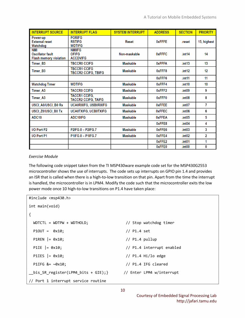
Each source of interrupt has its own entry in an interrupt vector table, and each ISR has a unique
identifier corresponding to an entry in this table so that the correct one is executed when an interrupt
occurs. By default, the ISRs over which the user has control are left blank without code so that the user
can fill it in and dictate the appropriate response to the interrupt.
When multiple sources of interrupt are triggered concurrently, interrupt priority is used to determine
the order of execution of the ISRs. Typically for a given microcontroller this priority is predetermined
and fixed for the different sources of interrupts. It is a good rule of thumb to keep the code in ISRs to a
minimum to avoid unexpected interruptions or missed interrupts when there are multiple sources of
interrupt enabled. The programmer must also be careful to write the ISR in such a way that there are no
errors caused when the interrupted code is resumed.
There are also two classes of interrupts: maskable and non-maskable. Maskable interrupts can be
enabled and disabled by the user at any time with the appropriate commands in the code. Whereas
non-maskable interrupts cannot be disabled by the user and typically have a priority higher than the
maskable ones since they occur as the result of critical events. An example of an event that causes a
non-maskable interrupt is the corruption of the on-board memory.
For reference, the interrupt vectors for the MSP430x2xx class of microcontrollers is shown below:
A Tutorial on Mobile Embedded Systems
10 Courtesy of Embedded Signal Processing Lab
http://jafari.tamu.edu
Exercise Module
The following code snippet taken from the TI MSP430ware example code set for the MSP430G2553
microcontroller shows the use of interrupts. The code sets up interrupts on GPIO pin 1.4 and provides
an ISR that is called when there is a high-to-low transition on that pin. Apart from the time the interrupt
is handled, the microcontroller is in LPM4. Modify the code such that the microcontroller exits the low
power mode once 10 high-to-low transitions on P1.4 have taken place:
#include <msp430.h>
int main(void)
{
WDTCTL = WDTPW + WDTHOLD; // Stop watchdog timer
P1OUT = 0x10; // P1.4 set
P1REN |= 0x10; // P1.4 pullup
P1IE |= 0x10; // P1.4 interrupt enabled
P1IES |= 0x10; // P1.4 Hi/lo edge
P1IFG &= ~0x10; // P1.4 IFG cleared
__bis_SR_register(LPM4_bits + GIE);} // Enter LPM4 w/interrupt
// Port 1 interrupt service routine
A Tutorial on Mobile Embedded Systems
11 Courtesy of Embedded Signal Processing Lab
http://jafari.tamu.edu
#pragma vector=PORT1_VECTOR
__interrupt void Port_1(void)
{
P1IFG &= ~0x10; // P1.4 IFG cleared
}
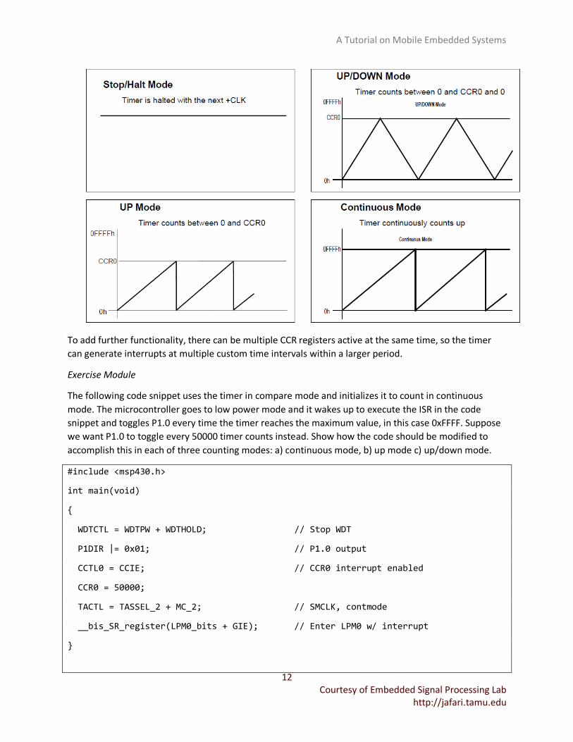
Timers Timers are basically counters that count at a fixed speed based on the local clock on the embedded
device. The timers can be used in two different modes based on their intended use:
Compare Mode In this mode a specific fixed count, known as the ‘compare value’ can be set up in a register by the user
and the timer count is continually compared with this number. As the timer counts up, whenever the
timer value matches the ‘compare value’ an interrupt is generated. In this way, interrupts can be
generated after a known amount of time or at repeated periodic intervals. This allows the system to
perform actions at scheduled regular intervals.
Often, the specific method of counting up and interrupt generation can also be configured. On the
MSP430 for example, there are 4 modes:
1. Stop/Halt Mode: The counter counts up to the designated value at the given clock speed and
then stops counting altogether.
2. Up/Down Mode: The timer counts up to the ‘compare value’, which is stored in a capture
compare register (CCR). Once this value is reached, the timer counts back down to zero at the
same rate, and then starts counting up again once zero is reached.
3. Up Mode: The timer counts up to the ‘compare value’ stored in the designated CCR register and
then instantaneously drops down to zero, before counting up again.
4. Continuous Mode: In this mode there is no ‘compare value’ and the timer simply counts up to
the maximum possible value, rolls over back to zero, and repeats the process continuously.
The 4 modes are illustrated in the figure below:
A Tutorial on Mobile Embedded Systems
12 Courtesy of Embedded Signal Processing Lab
http://jafari.tamu.edu
To add further functionality, there can be multiple CCR registers active at the same time, so the timer
can generate interrupts at multiple custom time intervals within a larger period.
Exercise Module
The following code snippet uses the timer in compare mode and initializes it to count in continuous
mode. The microcontroller goes to low power mode and it wakes up to execute the ISR in the code
snippet and toggles P1.0 every time the timer reaches the maximum value, in this case 0xFFFF. Suppose
we want P1.0 to toggle every 50000 timer counts instead. Show how the code should be modified to
accomplish this in each of three counting modes: a) continuous mode, b) up mode c) up/down mode.
#include <msp430.h>
int main(void)
{
WDTCTL = WDTPW + WDTHOLD; // Stop WDT
P1DIR |= 0x01; // P1.0 output
CCTL0 = CCIE; // CCR0 interrupt enabled
CCR0 = 50000;
TACTL = TASSEL_2 + MC_2; // SMCLK, contmode
__bis_SR_register(LPM0_bits + GIE); // Enter LPM0 w/ interrupt
}
A Tutorial on Mobile Embedded Systems
13 Courtesy of Embedded Signal Processing Lab
http://jafari.tamu.edu
// Timer A0 interrupt service routine
#pragma vector=TIMER0_A0_VECTOR
__interrupt void Timer_A (void)
{
P1OUT ^= 0x01; // Toggle P1.0
}
Capture Mode
In this mode the timer is continually counting up, and whenever a specific external event occurs the
timer count at that time is stored. In this way, the timing of external events can be captured. For
example, the time difference between two consecutive button presses can be measured by capturing
the timer count for each button press event and calculating the difference.
There is also a specialized timer on some microcontrollers called the Real-Time Clock (RTC). As the name
suggests, the purpose of this timer is to count out real world time; it supports registers for every
common time interval from a year, to a second and can also generate interrupts at intervals defined by
real time.
There is sometimes another specialized timer that plays an important role; on the MSP430 this timer is
called the ‘Watchdog Timer’. The role of this timer is to help the system reset if there is a catastrophic
error from which it cannot recover. A common scenario would be if the firmware flow left the processor
deadlocked in an unexpected state from which it cannot proceed. The watchdog timer can be set up to
expire after a pre-selected period to act as a fail-safe and reset the system in such situations.
Programmers must be aware that the timer could potentially be pre-configured with a default
countdown value which could cause unintended resets of the program if not dealt with. If the watchdog
functionality is not necessary, the timer can be disabled; it can then be potentially reconfigured to act as
a regular timer for general timing applications.
Exercise Module
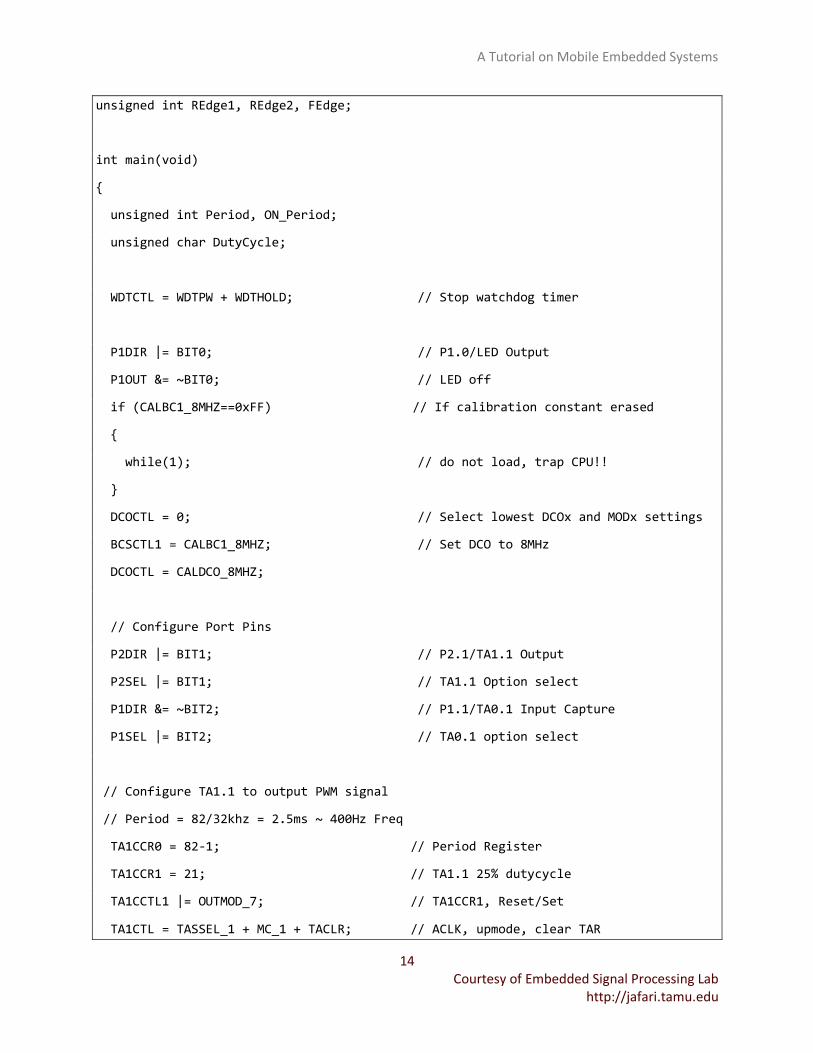
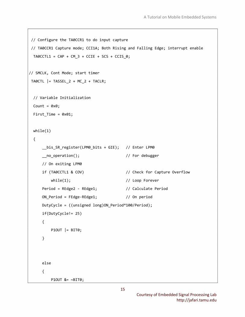
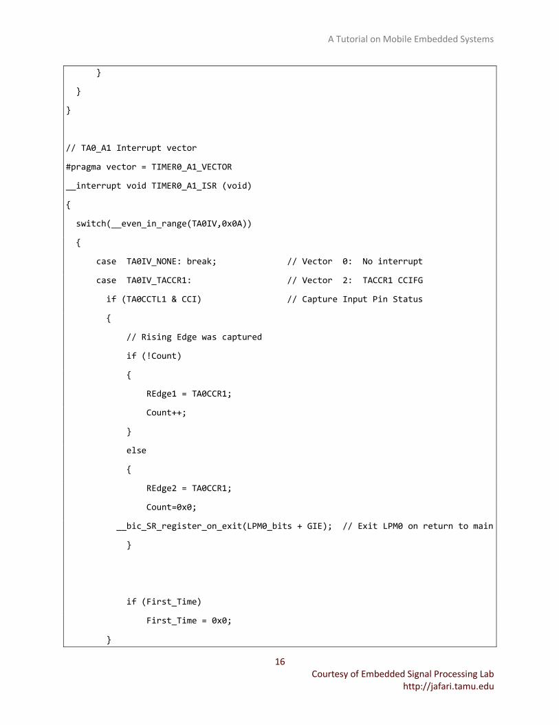
In the following code snippet, Timer A0 is used for input capture to measure the duty cycle of a signal
generated by Timer A1. Assume that the output of Timer A1 (on pin 2.1) is connected externally to the
input capture pin for Timer A0 (pin 1.2) to facilitate such a measurement. Gain an understanding of how
the code does this, and then modify it so that Timer A0 now only captures rising edges and uses this to
measure the period of the signal from Timer A1 instead.
#include <msp430.h>
unsigned char Count, First_Time;
A Tutorial on Mobile Embedded Systems
14 Courtesy of Embedded Signal Processing Lab
http://jafari.tamu.edu
unsigned int REdge1, REdge2, FEdge;
int main(void)
{
unsigned int Period, ON_Period;
unsigned char DutyCycle;
WDTCTL = WDTPW + WDTHOLD; // Stop watchdog timer
P1DIR |= BIT0; // P1.0/LED Output
P1OUT &= ~BIT0; // LED off
if (CALBC1_8MHZ==0xFF) // If calibration constant erased
{
while(1); // do not load, trap CPU!!
}
DCOCTL = 0; // Select lowest DCOx and MODx settings
BCSCTL1 = CALBC1_8MHZ; // Set DCO to 8MHz
DCOCTL = CALDCO_8MHZ;
// Configure Port Pins
P2DIR |= BIT1; // P2.1/TA1.1 Output
P2SEL |= BIT1; // TA1.1 Option select
P1DIR &= ~BIT2; // P1.1/TA0.1 Input Capture
P1SEL |= BIT2; // TA0.1 option select
// Configure TA1.1 to output PWM signal
// Period = 82/32khz = 2.5ms ~ 400Hz Freq
TA1CCR0 = 82-1; // Period Register
TA1CCR1 = 21; // TA1.1 25% dutycycle
TA1CCTL1 |= OUTMOD_7; // TA1CCR1, Reset/Set
TA1CTL = TASSEL_1 + MC_1 + TACLR; // ACLK, upmode, clear TAR
A Tutorial on Mobile Embedded Systems
15 Courtesy of Embedded Signal Processing Lab
http://jafari.tamu.edu
// Configure the TA0CCR1 to do input capture
// TA0CCR1 Capture mode; CCI1A; Both Rising and Falling Edge; interrupt enable
TA0CCTL1 = CAP + CM_3 + CCIE + SCS + CCIS_0;
// SMCLK, Cont Mode; start timer
TA0CTL |= TASSEL_2 + MC_2 + TACLR;
// Variable Initialization
Count = 0x0;
First_Time = 0x01;
while(1)
{
__bis_SR_register(LPM0_bits + GIE); // Enter LPM0
__no_operation(); // For debugger
// On exiting LPM0
if (TA0CCTL1 & COV) // Check for Capture Overflow
while(1); // Loop Forever
Period = REdge2 - REdge1; // Calculate Period
ON_Period = FEdge-REdge1; // On period
DutyCycle = ((unsigned long)ON_Period*100/Period);
if(DutyCycle!= 25)
{
P1OUT |= BIT0;
}
else
{
P1OUT &= ~BIT0;
A Tutorial on Mobile Embedded Systems
16 Courtesy of Embedded Signal Processing Lab
http://jafari.tamu.edu
}
}
}
// TA0_A1 Interrupt vector
#pragma vector = TIMER0_A1_VECTOR
__interrupt void TIMER0_A1_ISR (void)
{
switch(__even_in_range(TA0IV,0x0A))
{
case TA0IV_NONE: break; // Vector 0: No interrupt
case TA0IV_TACCR1: // Vector 2: TACCR1 CCIFG
if (TA0CCTL1 & CCI) // Capture Input Pin Status
{
// Rising Edge was captured
if (!Count)
{
REdge1 = TA0CCR1;
Count++;
}
else
{
REdge2 = TA0CCR1;
Count=0x0;
__bic_SR_register_on_exit(LPM0_bits + GIE); // Exit LPM0 on return to main
}
if (First_Time)
First_Time = 0x0;
}
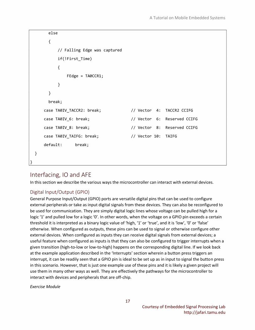
A Tutorial on Mobile Embedded Systems
17 Courtesy of Embedded Signal Processing Lab
http://jafari.tamu.edu
else
{
// Falling Edge was captured
if(!First_Time)
{
FEdge = TA0CCR1;
}
}
break;
case TA0IV_TACCR2: break; // Vector 4: TACCR2 CCIFG
case TA0IV_6: break; // Vector 6: Reserved CCIFG
case TA0IV_8: break; // Vector 8: Reserved CCIFG
case TA0IV_TAIFG: break; // Vector 10: TAIFG
default: break;
}
}
Interfacing, IO and AFE In this section we describe the various ways the microcontroller can interact with external devices.
Digital Input/Output (GPIO) General Purpose Input/Output (GPIO) ports are versatile digital pins that can be used to configure
external peripherals or take as input digital signals from these devices. They can also be reconfigured to
be used for communication. They are simply digital logic lines whose voltage can be pulled high for a
logic ‘1’ and pulled low for a logic ‘0’. In other words, when the voltage on a GPIO pin exceeds a certain
threshold it is interpreted as a binary logic value of ‘high, ‘1’ or ‘true’, and it is ‘low’, ‘0’ or ‘false’
otherwise. When configured as outputs, these pins can be used to signal or otherwise configure other
external devices. When configured as inputs they can receive digital signals from external devices; a
useful feature when configured as inputs is that they can also be configured to trigger interrupts when a
given transition (high-to-low or low-to-high) happens on the corresponding digital line. If we look back
at the example application described in the ‘Interrupts’ section wherein a button press triggers an
interrupt, it can be readily seen that a GPIO pin is ideal to be set up as in input to signal the button press
in this scenario. However, that is just one example use of these pins and it is likely a given project will
use them in many other ways as well. They are effectively the pathways for the microcontroller to
interact with devices and peripherals that are off-chip.
Exercise Module
A Tutorial on Mobile Embedded Systems
18 Courtesy of Embedded Signal Processing Lab
http://jafari.tamu.edu
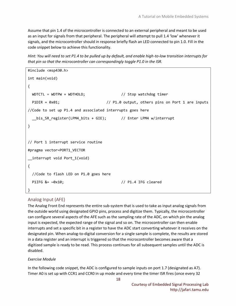
Assume that pin 1.4 of the microcontroller is connected to an external peripheral and meant to be used
as an input for signals from that peripheral. The peripheral will attempt to pull 1.4 ‘low’ whenever it
signals, and the microcontroller should in response briefly flash an LED connected to pin 1.0. Fill in the
code snippet below to achieve this functionality.
Hint: You will need to set P1.4 to be pulled up by default, and enable high-to-low transition interrupts for
that pin so that the microcontroller can correspondingly toggle P1.0 in the ISR.
#include <msp430.h>
int main(void)
{
WDTCTL = WDTPW + WDTHOLD; // Stop watchdog timer
P1DIR = 0x01; // P1.0 output, others pins on Port 1 are inputs
//Code to set up P1.4 and associated interrupts goes here
__bis_SR_register(LPM4_bits + GIE); // Enter LPM4 w/interrupt
}
// Port 1 interrupt service routine
#pragma vector=PORT1_VECTOR
__interrupt void Port_1(void)
{
//Code to flash LED on P1.0 goes here
P1IFG &= ~0x10; // P1.4 IFG cleared
}
Analog Input (AFE) The Analog Front End represents the entire sub-system that is used to take as input analog signals from
the outside world using designated GPIO pins, process and digitize them. Typically, the microcontroller
can configure several aspects of the AFE such as the sampling rate of the ADC, on which pin the analog
input is expected, the expected range of the signal and so on. The microcontroller can then enable
interrupts and set a specific bit in a register to have the ADC start converting whatever it receives on the
designated pin. When analog-to-digital conversion for a single sample is complete, the results are stored
in a data register and an interrupt is triggered so that the microcontroller becomes aware that a
digitized sample is ready to be read. This process continues for all subsequent samples until the ADC is
disabled.
Exercise Module
In the following code snippet, the ADC is configured to sample inputs on port 1.7 (designated as A7).
Timer A0 is set up with CCR1 and CCR0 in up mode and every time the timer ISR fires (once every 32
A Tutorial on Mobile Embedded Systems
19 Courtesy of Embedded Signal Processing Lab
http://jafari.tamu.edu
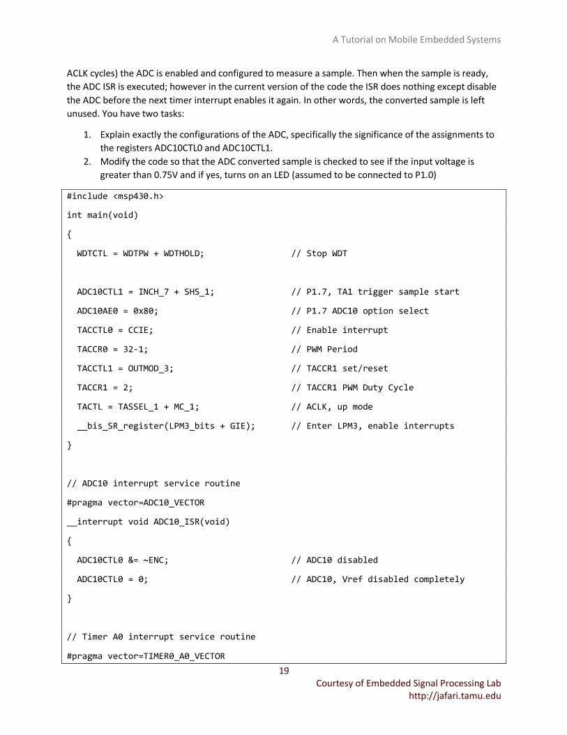
ACLK cycles) the ADC is enabled and configured to measure a sample. Then when the sample is ready,
the ADC ISR is executed; however in the current version of the code the ISR does nothing except disable
the ADC before the next timer interrupt enables it again. In other words, the converted sample is left
unused. You have two tasks:
1. Explain exactly the configurations of the ADC, specifically the significance of the assignments to
the registers ADC10CTL0 and ADC10CTL1.
2. Modify the code so that the ADC converted sample is checked to see if the input voltage is
greater than 0.75V and if yes, turns on an LED (assumed to be connected to P1.0)
#include <msp430.h>
int main(void)
{
WDTCTL = WDTPW + WDTHOLD; // Stop WDT
ADC10CTL1 = INCH_7 + SHS_1; // P1.7, TA1 trigger sample start
ADC10AE0 = 0x80; // P1.7 ADC10 option select
TACCTL0 = CCIE; // Enable interrupt
TACCR0 = 32-1; // PWM Period
TACCTL1 = OUTMOD_3; // TACCR1 set/reset
TACCR1 = 2; // TACCR1 PWM Duty Cycle
TACTL = TASSEL_1 + MC_1; // ACLK, up mode
__bis_SR_register(LPM3_bits + GIE); // Enter LPM3, enable interrupts
}
// ADC10 interrupt service routine
#pragma vector=ADC10_VECTOR
__interrupt void ADC10_ISR(void)
{
ADC10CTL0 &= ~ENC; // ADC10 disabled
ADC10CTL0 = 0; // ADC10, Vref disabled completely
}
// Timer A0 interrupt service routine
#pragma vector=TIMER0_A0_VECTOR
A Tutorial on Mobile Embedded Systems
20 Courtesy of Embedded Signal Processing Lab
http://jafari.tamu.edu
__interrupt void Timer_A(void)
{
ADC10CTL0 = SREF_1 + ADC10SHT_2 + REFON + ADC10ON + ADC10IE;
ADC10CTL0 |= ENC; // ADC10 enable set
}
Analog Output (DAC) The Digital to Analog Converter (DAC) can be used to reverse the process of the ADC and allow the
microcontroller to feed it appropriate signals digitally and have them converted to corresponding analog
voltages to be transmitted out. This can be used to drive devices such as a microphone which require an
analog input.
Communication Communication protocols on a microcontroller can be broadly divided into two categories: synchronous
and asynchronous.
Synchronous Communication This class of communication protocols is characterized by the presence of a shared digital clock signal
between the two communicating devices in addition to the lines used for communicating data. The clock
signal is typically used to ensure that the receiving device samples the transmitted data at the
appropriate time instances for correct interpretation. The two most commonly used synchronous
protocols are described below:
Serial Peripheral Interface (SPI)
Serial Peripheral Interface (SPI) involves communication between one master and one or more slave
devices. The devices can be comprised of any number of embedded microcontrollers or analog front
ends, with the designation of master and slave depending on the expected roles of each device. When
two or more devices are communicating using SPI, four hardware connections are required between
each master-slave pair; their names and functions are listed below:
1. Master Output Slave Input (MOSI) – Used to transmit bytes from master device to slave device
2. Master Input Slave Output (MISO) – Used to transmit bytes from slave device to master device
3. Serial Clock (SCLK) – Clock signal supplied by the master along with each transmitted byte to
synchronize slave’s sampling of each bit in the byte
4. Slave Select (SS) – When this line is pulled low, then the slave connected to this line is enabled
to actively communicate with the master.
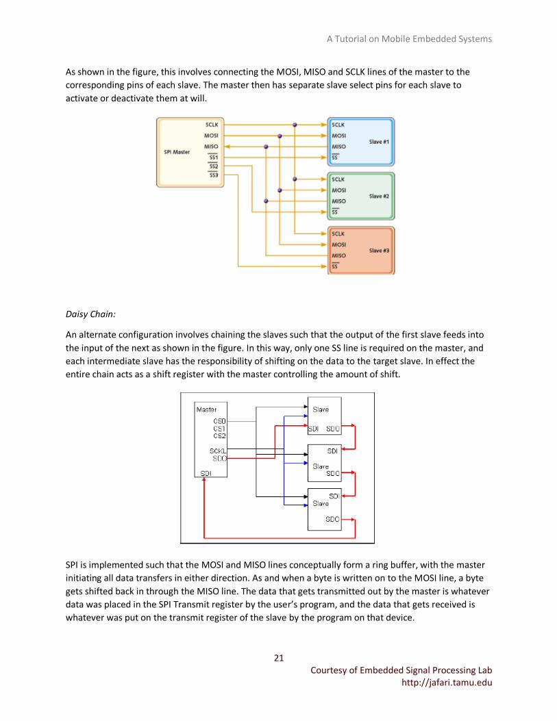
These connections are in parallel with corresponding ports on the master and slave connected together,
i.e., MOSI of master connected to MOSI of slave, MISO of master connected to MISO of slave and so on.
Since the functionality of the SS line is to choose the active slave, the hardware configuration varies
depending on the purpose. There are two commonly used configurations:
Independent Slaves:
A Tutorial on Mobile Embedded Systems
21 Courtesy of Embedded Signal Processing Lab
http://jafari.tamu.edu
As shown in the figure, this involves connecting the MOSI, MISO and SCLK lines of the master to the
corresponding pins of each slave. The master then has separate slave select pins for each slave to
activate or deactivate them at will.
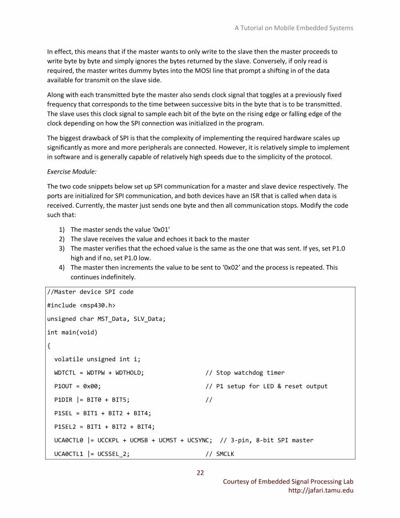
Daisy Chain:
An alternate configuration involves chaining the slaves such that the output of the first slave feeds into
the input of the next as shown in the figure. In this way, only one SS line is required on the master, and
each intermediate slave has the responsibility of shifting on the data to the target slave. In effect the
entire chain acts as a shift register with the master controlling the amount of shift.
SPI is implemented such that the MOSI and MISO lines conceptually form a ring buffer, with the master
initiating all data transfers in either direction. As and when a byte is written on to the MOSI line, a byte
gets shifted back in through the MISO line. The data that gets transmitted out by the master is whatever
data was placed in the SPI Transmit register by the user’s program, and the data that gets received is
whatever was put on the transmit register of the slave by the program on that device.
A Tutorial on Mobile Embedded Systems
22 Courtesy of Embedded Signal Processing Lab
http://jafari.tamu.edu
In effect, this means that if the master wants to only write to the slave then the master proceeds to
write byte by byte and simply ignores the bytes returned by the slave. Conversely, if only read is
required, the master writes dummy bytes into the MOSI line that prompt a shifting in of the data
available for transmit on the slave side.
Along with each transmitted byte the master also sends clock signal that toggles at a previously fixed
frequency that corresponds to the time between successive bits in the byte that is to be transmitted.
The slave uses this clock signal to sample each bit of the byte on the rising edge or falling edge of the
clock depending on how the SPI connection was initialized in the program.
The biggest drawback of SPI is that the complexity of implementing the required hardware scales up
significantly as more and more peripherals are connected. However, it is relatively simple to implement
in software and is generally capable of relatively high speeds due to the simplicity of the protocol.
Exercise Module:
The two code snippets below set up SPI communication for a master and slave device respectively. The
ports are initialized for SPI communication, and both devices have an ISR that is called when data is
received. Currently, the master just sends one byte and then all communication stops. Modify the code
such that:
1) The master sends the value ‘0x01’
2) The slave receives the value and echoes it back to the master
3) The master verifies that the echoed value is the same as the one that was sent. If yes, set P1.0
high and if no, set P1.0 low.
4) The master then increments the value to be sent to ‘0x02’ and the process is repeated. This
continues indefinitely.
//Master device SPI code
#include <msp430.h>
unsigned char MST_Data, SLV_Data;
int main(void)
{
volatile unsigned int i;
WDTCTL = WDTPW + WDTHOLD; // Stop watchdog timer
P1OUT = 0x00; // P1 setup for LED & reset output
P1DIR |= BIT0 + BIT5; //
P1SEL = BIT1 + BIT2 + BIT4;
P1SEL2 = BIT1 + BIT2 + BIT4;
UCA0CTL0 |= UCCKPL + UCMSB + UCMST + UCSYNC; // 3-pin, 8-bit SPI master
UCA0CTL1 |= UCSSEL_2; // SMCLK
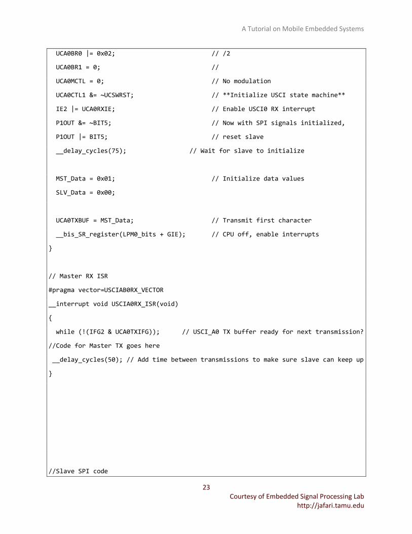
A Tutorial on Mobile Embedded Systems
23 Courtesy of Embedded Signal Processing Lab
http://jafari.tamu.edu
UCA0BR0 |= 0x02; // /2
UCA0BR1 = 0; //
UCA0MCTL = 0; // No modulation
UCA0CTL1 &= ~UCSWRST; // **Initialize USCI state machine**
IE2 |= UCA0RXIE; // Enable USCI0 RX interrupt
P1OUT &= ~BIT5; // Now with SPI signals initialized,
P1OUT |= BIT5; // reset slave
__delay_cycles(75); // Wait for slave to initialize
MST_Data = 0x01; // Initialize data values
SLV_Data = 0x00;
UCA0TXBUF = MST_Data; // Transmit first character
__bis_SR_register(LPM0_bits + GIE); // CPU off, enable interrupts
}
// Master RX ISR
#pragma vector=USCIAB0RX_VECTOR
__interrupt void USCIA0RX_ISR(void)
{
while (!(IFG2 & UCA0TXIFG)); // USCI_A0 TX buffer ready for next transmission?
//Code for Master TX goes here
__delay_cycles(50); // Add time between transmissions to make sure slave can keep up
}
//Slave SPI code
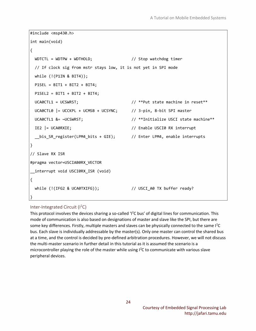
A Tutorial on Mobile Embedded Systems
24 Courtesy of Embedded Signal Processing Lab
http://jafari.tamu.edu
#include <msp430.h>
int main(void)
{
WDTCTL = WDTPW + WDTHOLD; // Stop watchdog timer
// If clock sig from mstr stays low, it is not yet in SPI mode
while (!(P1IN & BIT4));
P1SEL = BIT1 + BIT2 + BIT4;
P1SEL2 = BIT1 + BIT2 + BIT4;
UCA0CTL1 = UCSWRST; // **Put state machine in reset**
UCA0CTL0 |= UCCKPL + UCMSB + UCSYNC; // 3-pin, 8-bit SPI master
UCA0CTL1 &= ~UCSWRST; // **Initialize USCI state machine**
IE2 |= UCA0RXIE; // Enable USCI0 RX interrupt
__bis_SR_register(LPM4_bits + GIE); // Enter LPM4, enable interrupts
}
// Slave RX ISR
#pragma vector=USCIAB0RX_VECTOR
__interrupt void USCI0RX_ISR (void)
{
while (!(IFG2 & UCA0TXIFG)); // USCI_A0 TX buffer ready?
}
Inter-Integrated Circuit (I2C)
This protocol involves the devices sharing a so-called ‘I2C bus’ of digital lines for communication. This
mode of communication is also based on designations of master and slave like the SPI, but there are
some key differences. Firstly, multiple masters and slaves can be physically connected to the same I2C
bus. Each slave is individually addressable by the master(s). Only one master can control the shared bus
at a time, and the control is decided by pre-defined arbitration procedures. However, we will not discuss
the multi-master scenario in further detail in this tutorial as it is assumed the scenario is a
microcontroller playing the role of the master while using I2C to communicate with various slave
peripheral devices.
A Tutorial on Mobile Embedded Systems
25 Courtesy of Embedded Signal Processing Lab
http://jafari.tamu.edu
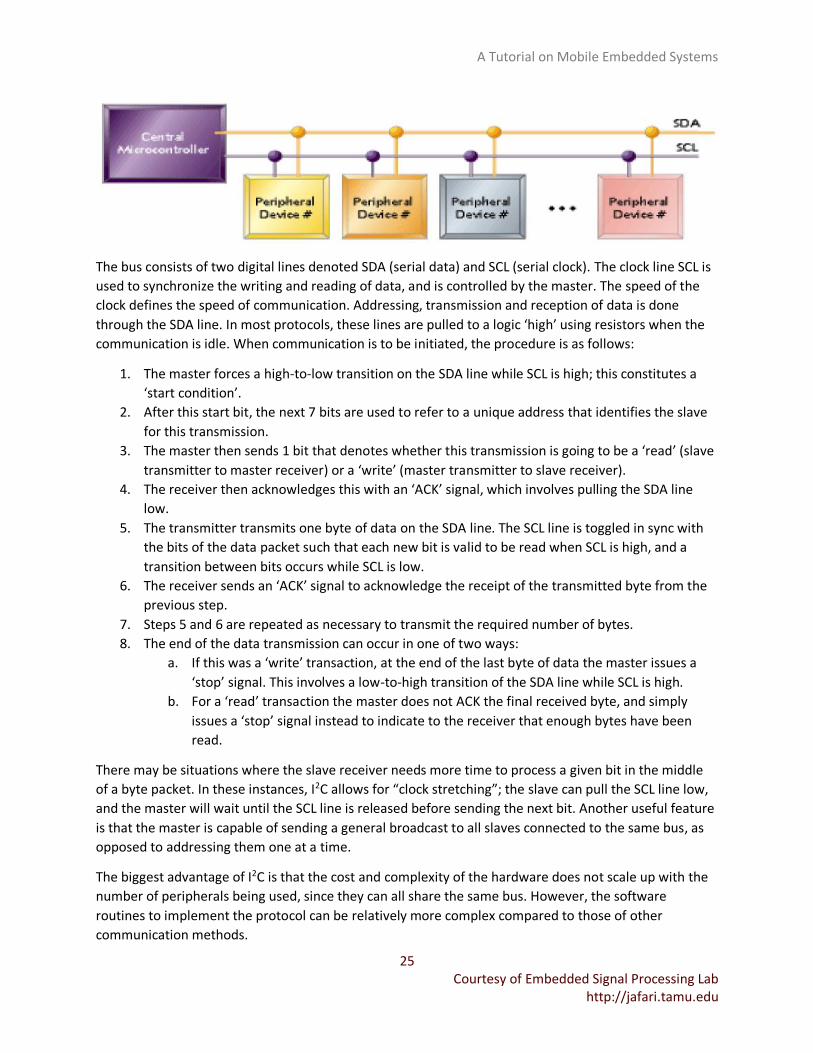
The bus consists of two digital lines denoted SDA (serial data) and SCL (serial clock). The clock line SCL is
used to synchronize the writing and reading of data, and is controlled by the master. The speed of the
clock defines the speed of communication. Addressing, transmission and reception of data is done
through the SDA line. In most protocols, these lines are pulled to a logic ‘high’ using resistors when the
communication is idle. When communication is to be initiated, the procedure is as follows:
1. The master forces a high-to-low transition on the SDA line while SCL is high; this constitutes a
‘start condition’.
2. After this start bit, the next 7 bits are used to refer to a unique address that identifies the slave
for this transmission.
3. The master then sends 1 bit that denotes whether this transmission is going to be a ‘read’ (slave
transmitter to master receiver) or a ‘write’ (master transmitter to slave receiver).
4. The receiver then acknowledges this with an ‘ACK’ signal, which involves pulling the SDA line
low.
5. The transmitter transmits one byte of data on the SDA line. The SCL line is toggled in sync with
the bits of the data packet such that each new bit is valid to be read when SCL is high, and a
transition between bits occurs while SCL is low.
6. The receiver sends an ‘ACK’ signal to acknowledge the receipt of the transmitted byte from the
previous step.
7. Steps 5 and 6 are repeated as necessary to transmit the required number of bytes.
8. The end of the data transmission can occur in one of two ways:
a. If this was a ‘write’ transaction, at the end of the last byte of data the master issues a
‘stop’ signal. This involves a low-to-high transition of the SDA line while SCL is high.
b. For a ‘read’ transaction the master does not ACK the final received byte, and simply
issues a ‘stop’ signal instead to indicate to the receiver that enough bytes have been
read.
There may be situations where the slave receiver needs more time to process a given bit in the middle
of a byte packet. In these instances, I2C allows for “clock stretching”; the slave can pull the SCL line low,
and the master will wait until the SCL line is released before sending the next bit. Another useful feature
is that the master is capable of sending a general broadcast to all slaves connected to the same bus, as
opposed to addressing them one at a time.
The biggest advantage of I2C is that the cost and complexity of the hardware does not scale up with the
number of peripherals being used, since they can all share the same bus. However, the software
routines to implement the protocol can be relatively more complex compared to those of other
communication methods.
A Tutorial on Mobile Embedded Systems
26 Courtesy of Embedded Signal Processing Lab
http://jafari.tamu.edu
Asynchronous Communication Asynchronous communication protocols do not require a shared clock signal between the two
communicating devices. The most widespread mode of asynchronous communication is the Universal
Asynchronous Receiver/Transmitter (UART) protocol which is described below.
Universal Asynchronous Receiver/Transmitter (UART) Protocol
In the UART protocol each data packet is a fixed size of one byte, and this byte is bracketed by a start bit
and a stop bit so that the receiving device knows when to read the data. Since there is no shared clock
to guide the reading of each data bit, the interpretation of the received data is based on previously
agreed upon communication speeds between the two devices. This speed of course is calculated by
each device based on its own local clock; so the expectation is that the relative error between the two
clocks is not so large that the receiving device interprets the data incorrectly. The communication speed
is typically reported as a ‘baud rate’. A ‘baud’ is a general term for a symbol in communication, and in
this context it refers to a single bit. Therefore a baud rate of 115200, means the UART communication
will transmit data at the rate of 115,200 bits every second.
UART requires only two connections between the two communicating devices. Each device has two
designated UART pins: a transmitting (TX) output port and a receiving (RX) input port. The TX port of
Device 1 is connected to the RX port of Device 2, and this is used for Device 1 to transmit data to Device
2. Similarly, the TX port of Device 2 is connected to the RX port of Device 1. Regardless of the nature of
either device, there is no designation of ‘master’ or ‘slave’ in terms of the communication as was the
case for SPI and I2C. In other words, both devices have equal control over the communication.
Both the UART lines are held high by default when communication is idle. Communication begins with a
‘start’ bit, which is merely pulling the sender’s TX line low. Data is then transmitted one byte at a time
from the sender’s transmit register at the agreed baud rate, and is received by the receiver on its RX line
and stored in a receive register.
The main advantage of UART is the simplicity of the hardware necessary: just two digital lines to
communicate between devices. It is also relatively simple to implement in firmware and there are
several existing solutions to convert UART to Bluetooth or USB protocol for other applications. The main
drawback is that it cannot really be used by one microcontroller to talk to multiple peripherals without
unduly complicating the hardware. Moreover, because of the lack of synchronizing clock, it is
susceptible to errors if there is a clock mismatch between devices. As one can imagine, this also means
that the UART is typically precluded from operating at very high speeds as the probability of error
increases as the time between successive bits reduces.
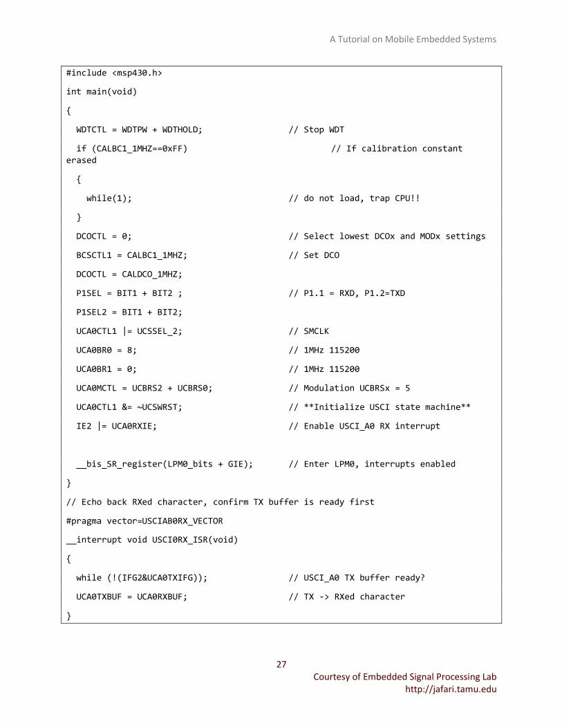
Exercise Module
The following code snippet initializes the microcontroller for UART communication at a baud rate of
115200, using the SMCLK as a 1MHz clock source. After UART is initialized, the microcontroller goes to
sleep and waits for a received character, which triggers the RX interrupt. The ISR then echoes back the
received character on the UART TX line. Modify the code to have the UART use a baud rate of 9600 with
the ACLK as the clock source instead. Assume that the ACLK speed is 32768Hz.
A Tutorial on Mobile Embedded Systems
27 Courtesy of Embedded Signal Processing Lab
http://jafari.tamu.edu
#include <msp430.h>
int main(void)
{
WDTCTL = WDTPW + WDTHOLD; // Stop WDT
if (CALBC1_1MHZ==0xFF) // If calibration constant
erased
{
while(1); // do not load, trap CPU!!
}
DCOCTL = 0; // Select lowest DCOx and MODx settings
BCSCTL1 = CALBC1_1MHZ; // Set DCO
DCOCTL = CALDCO_1MHZ;
P1SEL = BIT1 + BIT2 ; // P1.1 = RXD, P1.2=TXD
P1SEL2 = BIT1 + BIT2;
UCA0CTL1 |= UCSSEL_2; // SMCLK
UCA0BR0 = 8; // 1MHz 115200
UCA0BR1 = 0; // 1MHz 115200
UCA0MCTL = UCBRS2 + UCBRS0; // Modulation UCBRSx = 5
UCA0CTL1 &= ~UCSWRST; // **Initialize USCI state machine**
IE2 |= UCA0RXIE; // Enable USCI_A0 RX interrupt
__bis_SR_register(LPM0_bits + GIE); // Enter LPM0, interrupts enabled
}
// Echo back RXed character, confirm TX buffer is ready first
#pragma vector=USCIAB0RX_VECTOR
__interrupt void USCI0RX_ISR(void)
{
while (!(IFG2&UCA0TXIFG)); // USCI_A0 TX buffer ready?
UCA0TXBUF = UCA0RXBUF; // TX -> RXed character
}
A Tutorial on Mobile Embedded Systems
28 Courtesy of Embedded Signal Processing Lab
http://jafari.tamu.edu
Data Transmission and Storage
Transmission to External Device Certain applications require transmitting data to an external device such as a PC. We will go over two
commonly used options for accomplishing this here:
Bluetooth Serial Link The microcontroller can communicate the data to a Bluetooth chip which would then wirelessly transmit
to a PC using the standard Bluetooth protocol. On the receiving PC side it is interpreted as standard
serial data transmitted at the given baud rate just like UART. Moreover, the communication between
the microcontroller and the Bluetooth chip is also done using UART. In other words, these Bluetooth
modules have in-built firmware of their own that can convert incoming UART data into packets that
conform to the standard Bluetooth protocol; in the other direction, the Bluetooth module also converts
any incoming Bluetooth data into UART to be sent to the microcontroller. Therefore, as far as
programmers on the microcontroller and PC are concerned, this is in effect a UART connection between
the microcontroller and the PC at the designated baud rate. The Bluetooth module merely acts as a go-
between to make the connection wireless, which could be very useful for applications that require
untethered sensors.
Bluetooth modules available on the market commonly come with firmware pre-loaded for some basic
functionality. The default expected UART baud rate is usually set to 115200. The module is set up such
that as soon as it is powered on, it acts as a slave device and begins ‘advertising’; this means it is waiting
for a master device such as a PC to establish a connection. Once the module is advertising, the user can
usually use the PC to discover it as a new Bluetooth device and pair with it. After this process is
complete, the user has the info on which COM port# the module was assigned to on the PC. As
mentioned before, this is just like a serial connection to that COM port on the PC and can be used to
write a program on the PC for receiving data on that port. Although this is a common mode of operation
for these Bluetooth serial links, it is best to read the documentation of the specific module in question
to find details on the default start-up routine.
There is expected to be a hardware connection along the UART lines between the Bluetooth module and
the microcontroller. Just as was described in the previous section on UART, the TX line of the module is
connected to the RX line of the microcontroller and vice versa. Most likely, the same board that houses
the microcontroller and powers it will also be used to supply the requisite power to the Bluetooth
module.
It is also usually possible to interact with the Bluetooth module using the microcontroller to change
some settings on the module. For example, one common reason for change of the default firmware is
to change the baud rate. Most Bluetooth modules will document a specialized set of commands that can
be sent to it along the UART lines to have it make the appropriate changes to its firmware.
A specific example of such a Bluetooth module that can be used for quick prototyping is the Sparkfun
Bluetooth Mate Silver found here: https://www.sparkfun.com/products/12576
The board has a Bluetooth chip with pin-outs to supply power and two pins for UART TX and RX. Once
power is supplied to the board, the Bluetooth chip begins advertising and is discoverable by a PC. The PC
can pair with it and assign a COM port to it. The two UART pins can be connected to the UART pins of a

A Tutorial on Mobile Embedded Systems
29 Courtesy of Embedded Signal Processing Lab
http://jafari.tamu.edu
microcontroller. With the appropriate code on the microcontroller and PC, this simple hardware setup is
sufficient for the MSP430 to communicate wirelessly to the PC at a baud rate of 115200. A more
detailed step-by-step tutorial with documentation can be found here:
https://learn.sparkfun.com/tutorials/using-the-bluesmirf?_ga=1.172744867.1641870786.1462054224
Connecting the Bluetooth Mate to the MSP430 Launchpad
Here are step-by-step instructions for the hardware and firmware setup for a simple UART echo
application using the MSP430 Launchpad board and the Sparkfun Bluetooth Mate Silver BT module:
1. Flash the MSP430 Launchpad board using CCS (as described in the introductory section) and
download a suitable UART firmware.
2. You can use the example code given in the exercise problem of the previous ‘UART’ section in
this doc. This will set up UART on pins 1.1 (RX) and 1.2 (TX) of the Launchpad board with a baud
rate of 115200. The code will make the microcontroller echo back any character received by the
Launchpad.
3. Unplug the Launchpad (i.e. power it off) before completing the subsequent hardware
connections for safety. Use temporary jumper cables or solder wires to complete the
connections in steps 4 through 7.
4. Connect the ‘RX-I’ pin of the BT module to pin 1.2 of the Launchpad board.
5. Connect the ‘TX-O’ pin of the BT module to pin 1.1 of the Launchpad board.
6. Connect the VCC pin of the BT module to any available VCC pin on the Launchpad board
7. Connect the VCC pin of the BT module to any available VCC pin on the Launchpad board
8. Now plug in the Launchpad board to the PC using the mini-USB cable and it should power on
both the Launchpad as well as the BT module. A red LED on the BT module should be blinking to
indicate that it is advertising and waiting for a connection from the PC.
9. Follow the instructions in the SparkFun tutorial under the section ‘Connecting to the Modem in
Windows’ to pair your BT module with your PC (Link to tutorial:
https://learn.sparkfun.com/tutorials/using-the-
bluesmirf?_ga=1.172744867.1641870786.1462054224)
10. Once the BT module is paired to the PC it will be associated with a COM port on that PC for all
future serial links. Find the COM port number by going to ‘Devices and Printers’, right-clicking on
your BT module’s name and looking at the Hardware Properties.
11. On the PC open PuTTY (download and install this free software if unavailable on your computer).
Set up a ‘Serial’ connection at a baud rate of 115200 with the COM port # identified earlier.
12. After entering these settings on the main PuTTY screen, also go to the ‘Serial’ section of the
PuTTY window (located on the left) and change the ‘Flow Control’ setting to ‘None’ if it is not
already.
13. Click ‘Open’ and this should open the connection on the PuTTY window with a blank terminal
screen. The LED on the BT module should also be a solid green indicating a successful
connection
14. Now any character you type on the keyboard will be sent to the MSP430 via Bluetooth, and it
will be echoed back to your screen on the terminal window.
A Tutorial on Mobile Embedded Systems
30 Courtesy of Embedded Signal Processing Lab
http://jafari.tamu.edu
Data Storage While by no means comparable in size to the memory available on a PC, microcontrollers typically do
have a certain amount of non-volatile memory, i.e., memory that will still be available even after the
device has been power cycled (turned off and back on). For example, the MSP430G2553 microcontroller
that is on the Launchpad board has 16kB of flash memory. Typical uses of this memory would be to
store a relatively small amount of data, or certain numerical constants that are used in the program
itself. For example, if a physiological monitoring device has been calibrated according to certain physical
parameters of the subject, these parameters can be stored in the flash memory for easy retrieval in the
future.
There are a few things to keep in mind when working with flash memory. Typically, flash memory is
partitioned into segments. On the MSP430, these segments of main memory are of size 512 bytes,
meaning the MSP430G2553 has 32 such segments to give a total main memory of 16kB. Due to the
hardware architecture of flash memory, writing to and deleting from memory work differently. The
programmer can write can typically write anything from one bit (the smallest unit), a byte or even one
word (2 bytes, in the case of this microcontroller) at a time. However, erasing from memory can only be
done in segments. In other words, in order to erase even 1 byte of memory, the entire corresponding
512-byte segment needs to be erased. Therefore if less than 1 segment needs to be erased, the
remaining data needs to be written temporarily into a different part of memory in order to save it and
write it back after the erase.
The programmer needs to be well aware of the organization and size of the flash memory being used,
and also needs to be comfortable coding using pointers to flash memory. An important thing to keep in
mind is that the code to be executed by the microcontroller is also stored in the same flash memory,
thus reducing the effective size available for data storage, as well as increasing the risk of unintended
memory corruption. However, once the programmer becomes familiar with Flash memory, it can be a
useful tool for several applications.
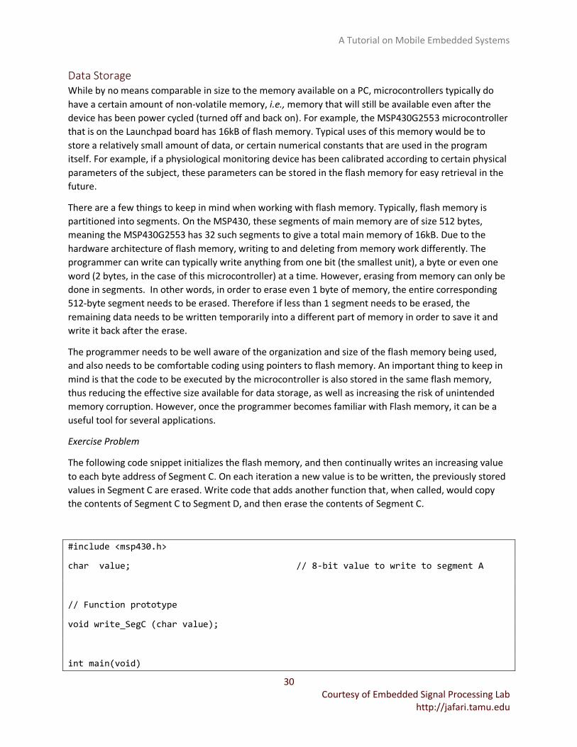
Exercise Problem
The following code snippet initializes the flash memory, and then continually writes an increasing value
to each byte address of Segment C. On each iteration a new value is to be written, the previously stored
values in Segment C are erased. Write code that adds another function that, when called, would copy
the contents of Segment C to Segment D, and then erase the contents of Segment C.
#include <msp430.h>
char value; // 8-bit value to write to segment A
// Function prototype
void write_SegC (char value);
int main(void)
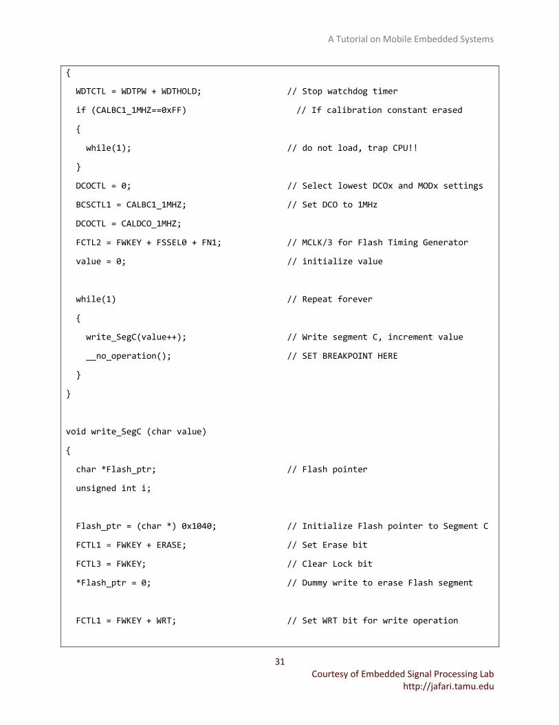
A Tutorial on Mobile Embedded Systems
31 Courtesy of Embedded Signal Processing Lab
http://jafari.tamu.edu
{
WDTCTL = WDTPW + WDTHOLD; // Stop watchdog timer
if (CALBC1_1MHZ==0xFF) // If calibration constant erased
{
while(1); // do not load, trap CPU!!
}
DCOCTL = 0; // Select lowest DCOx and MODx settings
BCSCTL1 = CALBC1_1MHZ; // Set DCO to 1MHz
DCOCTL = CALDCO_1MHZ;
FCTL2 = FWKEY + FSSEL0 + FN1; // MCLK/3 for Flash Timing Generator
value = 0; // initialize value
while(1) // Repeat forever
{
write_SegC(value++); // Write segment C, increment value
__no_operation(); // SET BREAKPOINT HERE
}
}
void write_SegC (char value)
{
char *Flash_ptr; // Flash pointer
unsigned int i;
Flash_ptr = (char *) 0x1040; // Initialize Flash pointer to Segment C
FCTL1 = FWKEY + ERASE; // Set Erase bit
FCTL3 = FWKEY; // Clear Lock bit
*Flash_ptr = 0; // Dummy write to erase Flash segment
FCTL1 = FWKEY + WRT; // Set WRT bit for write operation
A Tutorial on Mobile Embedded Systems
32 Courtesy of Embedded Signal Processing Lab
http://jafari.tamu.edu
for (i=0; i<64; i++)
{
*Flash_ptr++ = value; // Write value to flash
}
FCTL1 = FWKEY; // Clear WRT bit
FCTL3 = FWKEY + LOCK; // Set LOCK bit
}
A Tutorial on Mobile Embedded Systems
33 Courtesy of Embedded Signal Processing Lab
http://jafari.tamu.edu
Appendix: Useful Resources The following documents are useful references for details on the various concepts and devices discussed
in the tutorial:
Code Composer Studio User’s Guide: More details on how to use the various features of Code
Composer for downloading and debugging your code.
MSP430G2553 Datasheet: Electrical characteristics and other detailed information of the
MSP430 chip itself, including its various peripherals
MSP430G2553 User’s Guide: User’s Guide for the MSP430x2xx family of microcontrollers, with
descriptions of the various peripherals including the register maps.
MSP-EXP430G2 Quick Start Guide for the Launchpad board
MSP-EXP430G2 User’s Guide: User’s Guide for the entire integrated Launchpad board


![Embedded JPEG Slide Show Tutorialdjsiw1wjy8vi7.cloudfront.net/[SDK2.5]Documents_Tutorials/Tutorial...Embedded JPEG Slide Show Tutorial ... Resources/icons/tut_106.png](https://img.pdfslide.us/doc/110x75/5af4df527f8b9a95468e8c6c/embedded-jpeg-slide-show-t-sdk25documentstutorialstutorialembedded-jpeg-slide.jpg)