Embed Size (px)
Citation preview
TOWARDS A TRANSPARENT PHOTOVOLTAIC FILMA TECHNOLOGICAL APPROACH WITH THE ETFE
RELATRICEPROFESSORESSA ALESSANDRA ZANELLI
TESI DI STEFANO PIONTINI725298
A.A. 2010-2011
FACOLTÀ DI ARCHITETTURA E SOCIETÀLAUREA MAGISTRALE IN ARCHITETTURA - LANDSCAPE AND CONCENTRATION

2

3
un ringraziamento particolare va alla Professoressa Zanelli che ha creduto in me durante tutto il mio percorso universitario
4
Table of contents
Introduction 7
ETFE 13 History 14 -Eden Project, 2001 15 Performances 17 Projects and use of ETFE 23 -2008: the Olympic games in Beijing 23 -The Bird’s Nest 24 -The Watercube 28 -Material for an Architectural Revolution 31 -Unilever Headquarter 34 -Palazzo Lombardia 37 -New Waitomo Caves Visitor Centre 41
Thin Photovoltaic Films 45 analysis of technologies 46 present research lines in Europe 47 thin films 49 Amorphous Silicon 51 - application of aSi PV 58 CGIS Photovoltaic 63 CdTe Photovoltaic 69
Transparent Photovoltaic films 75 aSi-T 76 is Organic PV the future of solar? 79 Organic Photovoltaic 81 - San Francisco MTA transit shelter 87

5
Spherical Photovoltaic 89
Photovoltaic integrated ETFE 93 A dynamic Architecture 94 Gazeley Logistic Warehouse 97 Solar Next 104 SMIT Sustainably Minded Interactive Technology 111 Bibliography 116


INTRODUCTION
8
Sustainable architecture is a general term that describes environmentally conscious design techniques in the fi eld of architecture. Sustainable architecture is framed by the larger discussion on sustainability and the pressing economic and political issues of our world. In the broad context, it seeks to minimize the nega-tive environmental impact of buildings by enhancing effi ciency and moderation in the use of materials, energy, and development space. Most simply, the idea of sustainability, or ecological design, is to ensure that our actions and decisions today do not inhibit the opportunities of future generations. Th is term can be used to describe an energy and ecologically conscious approach to the design of the built environment.
Th is defi nition of the sustainable architecture is a starting point which identifi es the new role of the architect in our century: not only a designer, not only a constructor, not only an engi-neer. Th e new architect has to combine style, structures, territorial links, to an idea of envi-ronmental respect and to an eye on the future and on the developments that the new technolo-gies produce.Buildings are not more made to resist for ages, just only until you found a new better techno-logy to improve them and their performances, like a machine that receive an upgrade of one part. Th is is an important point because the city, with that new rule, becomes a lab where you could experiment, change, develop, improve technologies and styles. A fl uid dynamic place where architects, within the limits of laws, show their experiences and their feelings.During my last two year in Politecnico I had the chance to know the China reality, in particu-lar the city of Shanghai: this is an example of a fl exible city, an extreme one.To build in Shanghai you have three weeks to project and three weeks to build: the people there goes two times faster because they know to reach the West they have to run and fi ll the gap between these two worlds. In this economical boom they see the dark side of this run: pollution increase, traffi c of vehicles goes out of control, the population increase too much and too fast, the resources won’t satisfy all the population. Th ey know this problem but for now the authorities are not able to solve it: they control the media and all the internet with a strong fi lter, just to not give information not approved from the government, and there’s a law that increase taxes for the couple who wants more than one baby; this last decision on population

9
wants to control the use of territory in order to indirectly reduce the pollution and directly the consumption of the resources, just to not raise a debt too large with other countries.Th e Chinese situation, similar to the Indian one, or in future for the African countries, is a big alarm for the world and the United Nations have promulgated from the ’80 a document that defi ne the guidelines for the next century to reach in order to control and prevent the collapse of the earth system. Th is document is the Agenda 21, which is a comprehensive plan of action to be taken globally, nationally and locally by organizations of the United Nations System, Governments, and Major Groups in every area in which human impacts on the environment. Agenda 21, the Rio Declaration on Environment and Development, and the Statement of principles for the Sustainable Management of Forests were adopted by more than 178 Go-vernments at the United Nations Conference on Environment and Development (UNCED) held in Rio de Janeiro, Brazil, on June 1992.Th e full implementation of Agenda 21, the Program for Further Implementation of Agenda 21 and the Commitments to the Rio principles, were strongly reaffi rmed at the World Summit on Sustainable Development held in South Africa in 2002.Agenda 21 addresses the pressing problems of today and also aims at preparing the world for the challenges of the next century. It refl ects a global consensus and political commitment at the highest level on development and environment cooperation. Its successful implementation is fi rst and foremost the responsibility of Governments. National strategies, plans, policies and processes are crucial in achieving this. International cooperation should support and supple-ment such national eff orts. In this context, the United Nations system has a key role to play. Other international, regional and sub regional organizations are also called upon to contribute to this eff ort. Th e broadest public participation and the active involvement of the non-go-vernmental organizations and other groups should also be encouraged.Th is is one of the most important extract from the preamble of the document, because it put the accent over the responsibilities of every nation in front of the environment cooperation, let every signed country to promote new technologies and to develop bonuses to involve people to approach the new green technologies.In Italy for example we see a large use of incentives for new cars if the people recycle the old one, or bonus for new appliances without greenhouse gases or for solar panels integrated sy-stems: the solar energy is one of the best solution for our country, which is one with the largest
10
number of sunny days along the year in Europe. Th is is also one of the cheapest solutions for sustainable energy, and one with the lowest impact on territory, in particular in an urban situa-tion.Th e solar energy opens diff erent uses of the energy, from heating, to hot water or photovoltaic, and is now one of the most developed, also from big petrol companies, that see it as a future way of sustainable energy with low costs and high effi ciency on the medium-long period, in order to justify the fi rst investment.Photovoltaic energy represents an important resource for the production of electric energy, in particular because today this fundamental power is produced by petrol, nuclear fi ssion and hydro-electric centrals and a new clean energy like the solar could implement the off er and in certain places change the hierarchy.Another important sustainable issue is concerning the materials and their production. One general mistake is to think that if a material is sustainable for U.S., it has to be sustainable for Italy: this is not true, because if I buy that material in a range of few km from the production, I have a sustainable product, but if I buy it from the other side of the world, it couldn’t be sustai-nable, just only for the transportation. Th e research today has the possibility to discover incredible solutions for construction and it has the potential to adapt well known natural materials with the modern requests for the sustainability and the fl exibility of the buildings. Today we could use a textile as a structural element, like glass, and a glue could be more resistant than a screw or a bolt. In this prospective, I’ve had the chance, here in Politecnico, to study the proprieties of a dif-ferent range of materials and aft er a course with the professor Alessandra Zanelli, I have analyzed the tensile and I’ve focus my attention on ETFE, a sustainable plastic, 100% recycla-ble, Th e production of the ETFE has made with a base of water and it’s produced in thin fi lms, thanks to his extreme thickness and his strength, that made it one of the lightest structural material. Another important point is the translucency and the elevated strength against chemi-cal agents, so this is why today architects like Herzog & De Meuron approach this material for their projects. Th e fl exibility of the ETFE gives it also the possibility to integrate this fi lm with a renewable energy system like the photovoltaic thin fi lms, making a tensile totally sustainable and produ-
11
cer of elettric energy. I’ve started to approach this solution four years ago, when only one little fi rm in Germany, called Solar-Next, begun to commercialize this product. Today this techno-logy is no more developed and my research try to make the new step that this technology needs to become accessible: when in February the magazine Elementi asked me to speak in a conference to explain my fi rst thesis on this product, I realized that the knowledge of ETFE-Photovoltaic system is today only an idea and my wish is to arrive at the end of this thesis to demonstrate that this solution is real and could have incredible evolutions in few years, just for the fast development of photovoltaics thin fi lms and for the optimization of the production of ETFE, reducing also the cost of the tensile.
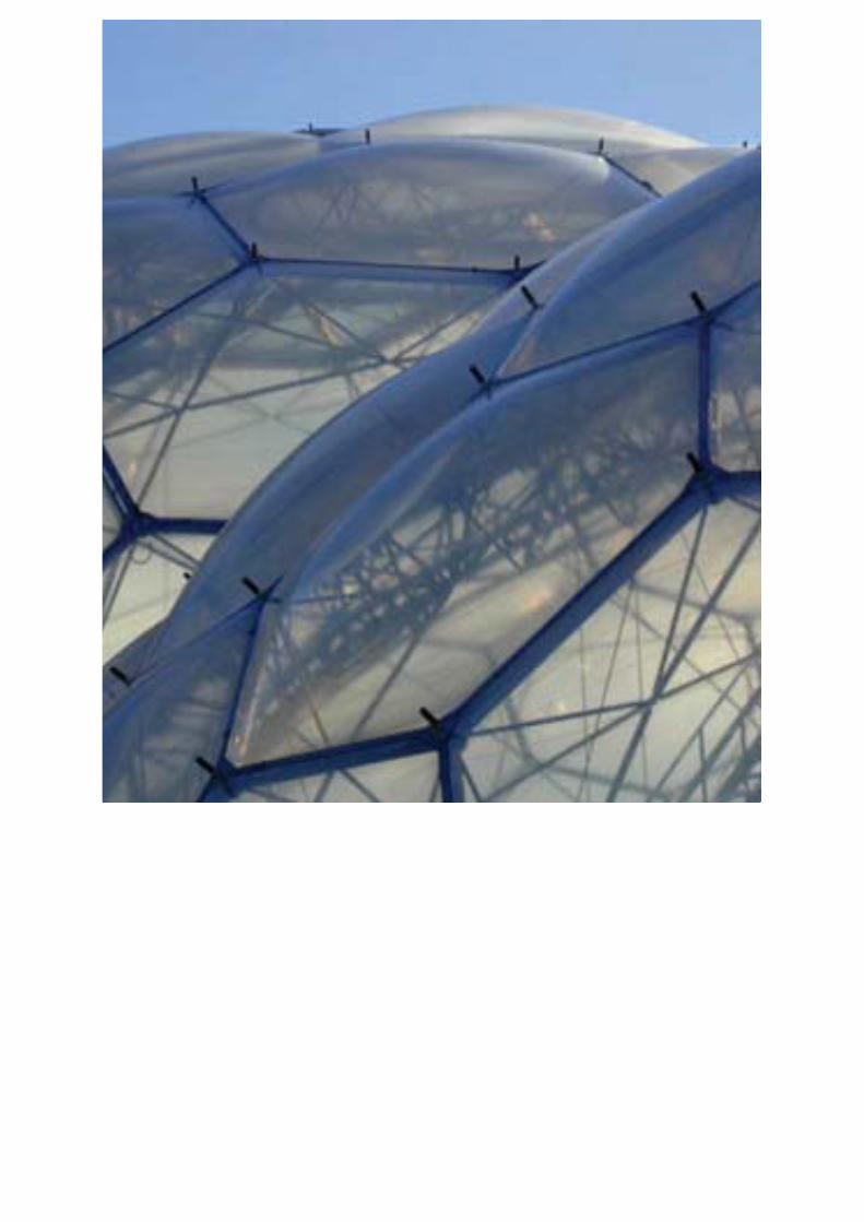

ETFE
14
Th e ETFE is a fl uorine based plastic and its systematic name is polyethylene-co-tetrafl uoro-ethylene, because this polymer is based on the link fl uorine-carbon. Compared to glass, ETFE fi lm is 1% the weight, transmits more light and costs 24% to 70% less to install. It’s also resilient, able to bear 400 times its own weight, self-cleaning (due to its nonstick surface) and recyclable. On the other hand it is prone to punctures by sharp edges, therefore it is mostly used for roofs. In sheet form as commonly employed for architecture, it is able to stretch to three times its length without loss of elasticity. Employing heat welding, tears can be repaired with a patch or multiple sheets assembled into larger panels. Th is “sewing” me-thod enables ETFE to be installed in pieces much longer and wider than glass: a strip of ETFE could be 54,90m long and 3,66m wide. When exposed to fi re, it soft ens and shrinks away from the heat, naturally venting smoke out of a building.
History
It was originally designed around the 1970s, when DuPont, a leader producer of plastic ele-ments, invented a fl uorocarbon-based polymer to be used as an insulation material in the aero-nautics industry, in order to solve the needs of a material with high corrosion resistance and strength over a wide temperature range.DuPont did not initially care about marketing ETFE to architects: it was Stefan Lehnert, a German mechanical engineering, in his search for new sailing technologies, who saw building-material potentials in its transparency, in its self-cleaning and structural properties. In 1982, he founded Vector Foiltec, a design and manufacturing company, specializing in the use of ETFE, in Bremen, Germany. Th e company’s fi rst project was the roof of a small pavilion at a zoo in Arnheim, Holland. Since then, ETFE has become increasingly popular, especially in Europe, and this new polymer was widely used in offi ce atriums, some educational buildings, medical facilities, exposition halls, and zoos across Britain and Germany. In 2000, the Eden Project, an environmental complex in Cornwall, Britain, designed by Grimshaw Architects and containing two gigantic geodesic conservatories covered in ETFE, was completed. Th e construction was acclaimed as an engineering marvel and created a wave of global interest. Th e interesting property for architects is that the resin can be spun into a thin, durable fi lm,
15
which manufacturers such as DuPont Tefzel and Asahi Glass Company, which calls its version Fluon, pack in rolls. It can be used in sheets or infl ated into cushions. An example of its actual use is as pneumatic panels to cover the outside of the football stadium Allianz Arena in Ger-many or the Beijing National Aquatics Centre, the world’s largest structure made of ETFE fi lm (laminate).
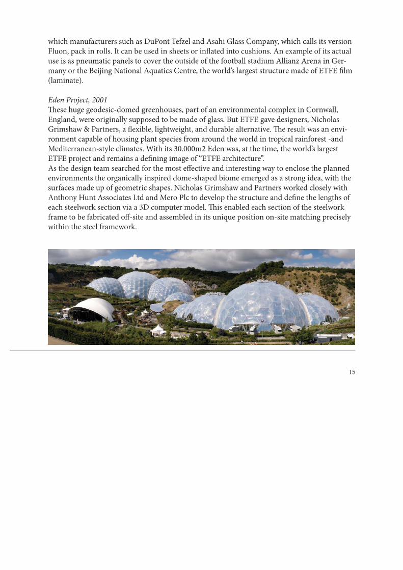
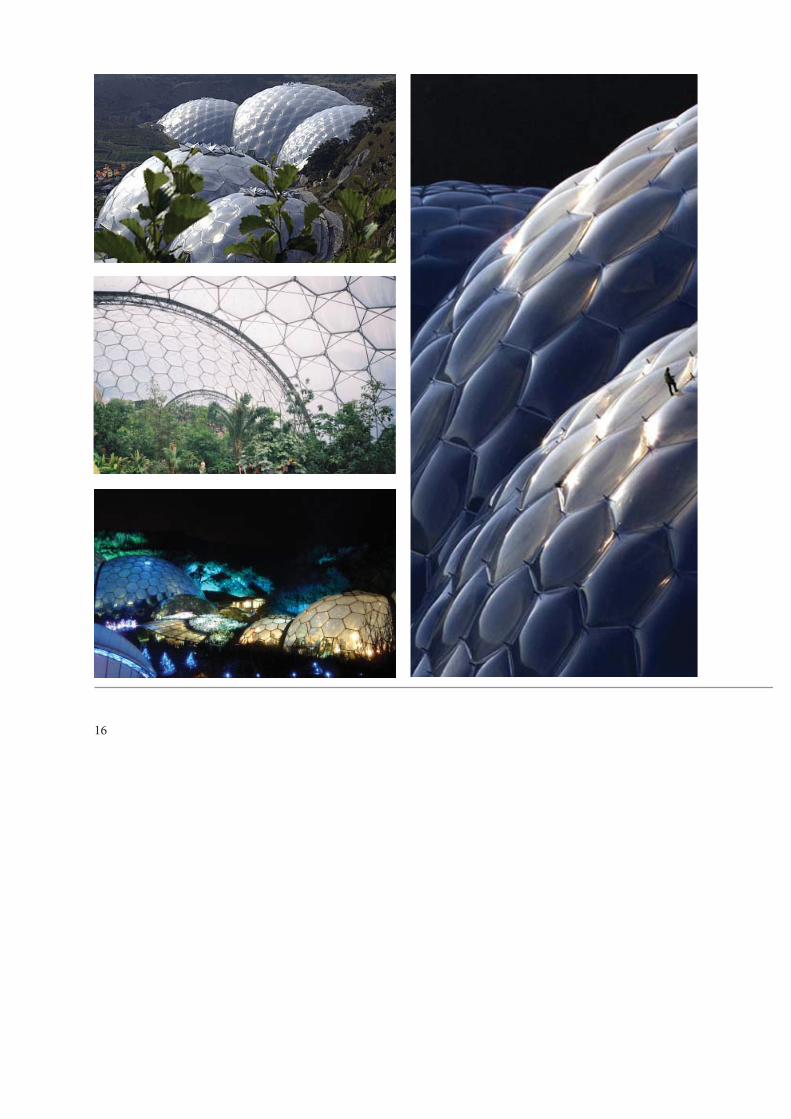
Eden Project, 2001Th ese huge geodesic-domed greenhouses, part of an environmental complex in Cornwall, England, were originally supposed to be made of glass. But ETFE gave designers, Nicholas Grimshaw & Partners, a fl exible, lightweight, and durable alternative. Th e result was an envi-ronment capable of housing plant species from around the world in tropical rainforest -and Mediterranean-style climates. With its 30.000m2 Eden was, at the time, the world’s largest ETFE project and remains a defi ning image of “ETFE architecture”.As the design team searched for the most eff ective and interesting way to enclose the planned environments the organically inspired dome-shaped biome emerged as a strong idea, with the surfaces made up of geometric shapes. Nicholas Grimshaw and Partners worked closely with Anthony Hunt Associates Ltd and Mero Plc to develop the structure and defi ne the lengths of each steelwork section via a 3D computer model. Th is enabled each section of the steelwork frame to be fabricated off -site and assembled in its unique position on-site matching precisely within the steel framework.
16
17
Th e fi nal architectural and structural design is hugely effi cient, providing maximum strength with minimum steelwork and maximum volume with minimum surface area. Th e transparent hexagonal membranes transmit more light than glass and the largest biome spans more than one hundred meters without requiring internal supports - allowing complete freedom for the landscape architects and horticulturalists.
Performances
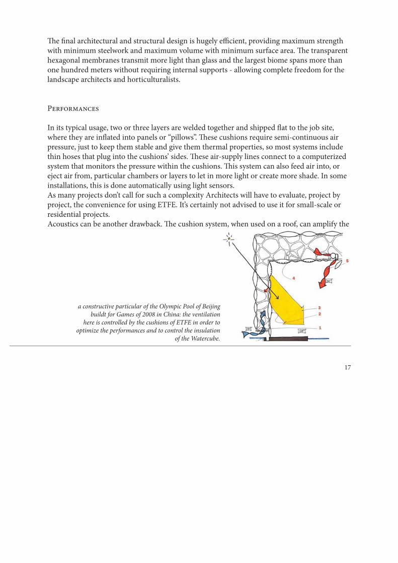
In its typical usage, two or three layers are welded together and shipped fl at to the job site, where they are infl ated into panels or “pillows”. Th ese cushions require semi-continuous air pressure, just to keep them stable and give them thermal properties, so most systems include thin hoses that plug into the cushions’ sides. Th ese air-supply lines connect to a computerized system that monitors the pressure within the cushions. Th is system can also feed air into, or eject air from, particular chambers or layers to let in more light or create more shade. In some installations, this is done automatically using light sensors. As many projects don’t call for such a complexity Architects will have to evaluate, project by project, the convenience for using ETFE. It’s certainly not advised to use it for small-scale or residential projects.Acoustics can be another drawback. Th e cushion system, when used on a roof, can amplify the
a constructive particular of the Olympic Pool of Beijing buildt for Games of 2008 in China: the ventilation
here is controlled by the cushions of ETFE in order to optimize the performances and to control the insulation
of the Watercube.
18
sound of rain because the tension in the cushion acts like a drum. Manufacturers have deve-loped several noise-suppressing techniques, including layering polycarbonate sheets within ETFE cushions, but their use isn’t widespread yet. Interior applications, such as walls within an offi ce, present other sound issues. ETFE transmits more sound than glass or wood, making it not convenient for meeting rooms, or conference centres. In opposition, ETFE can be bene-fi cial for self-contained, noisy areas like aquatic parks -sound bounces off the walls and fl oor and escapes through the roof.ETFE is a thermoplastic fl uoropolymer, in particular is a copolymer comprising of tetrafl uoro-ethylene (C2F4) and ethylene (C2H4).
H H F F | | | | ••• -C-C-C-C- ••• | | | | H H F F
It’s also a balanced one that has chemical resistance and electrical properties comparable to typical fl uoropolymer, such as PTFE, PFA and FEP and also is more progressive than ECTFE or PVdF with its improved mechanical strength.Translucency of the ETFE membrane is about 95 % within the range of 400 - 600 Nm, with scattered light at a proportion of 12 % and direct light at a proportion of 88 %. For a three-lay-ered module (upper layer 200μm, middle layer 100μm, inner layer 200μm), the degree of light transmission for vertical incidence is = 0.7. Th is range represents the translucency characteri-stics important for life (of humans, animals and plants). Compared to open air environment the dangerous UV-B and UV-C radiation (which causes burning and is carcinogenic) is consi-derably reduced by fi ltration.
u-values are as follows (depending on test procedures these values may vary considerably):- for one-layered membranes ≈ 5.1 W/m²K- for two-layered membranes ≈ 3.5 W/m²K- for three-layered membranes ≈ 2.0 W/m²K
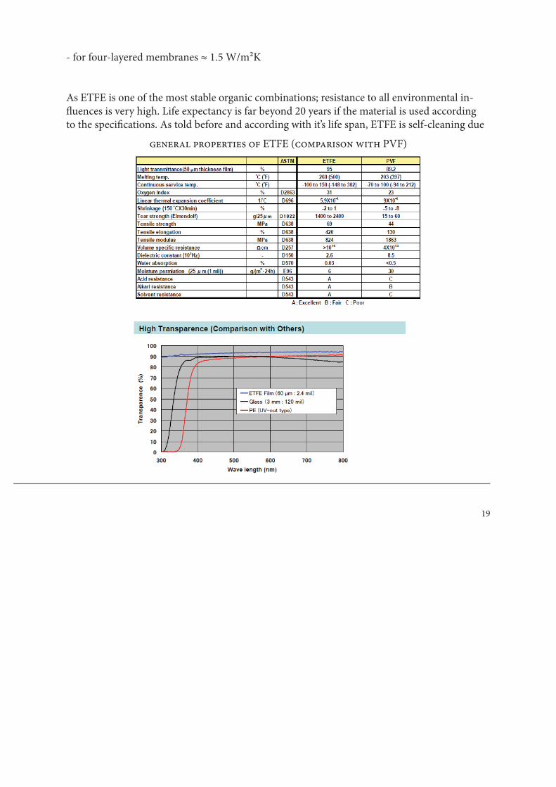
19
- for four-layered membranes ≈ 1.5 W/m²K
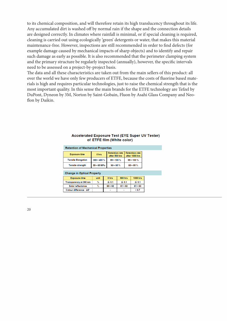
As ETFE is one of the most stable organic combinations; resistance to all environmental in-fl uences is very high. Life expectancy is far beyond 20 years if the material is used according to the specifi cations. As told before and according with it’s life span, ETFE is self-cleaning due
general properties of ETFE (comparison with PVF)
20
to its chemical composition, and will therefore retain its high translucency throughout its life. Any accumulated dirt is washed off by normal rain if the shape and the connection details are designed correctly. In climates where rainfall is minimal, or if special cleaning is required, cleaning is carried out using ecologically ‘green’ detergents or water, that makes this material maintenance-free. However, inspections are still recommended in order to fi nd defects (for example damage caused by mechanical impacts of sharp objects) and to identify and repair such damage as early as possible. It is also recommended that the perimeter clamping system and the primary structure be regularly inspected (annually), however, the specifi c intervals need to be assessed on a project-by-project basis. Th e data and all these characteristics are taken out from the main sellers of this product: all over the world we have only few producers of ETFE, because the costs of fl uorine based mate-rials is high and requires particular technologies, just to raise the chemical strength that is the most important quality. In this sense the main brands for the ETFE technology are Tefzel by DuPont, Dyneon by 3M, Norton by Saint-Gobain, Fluon by Asahi Glass Company and Neo-fl on by Daikin.
21
22
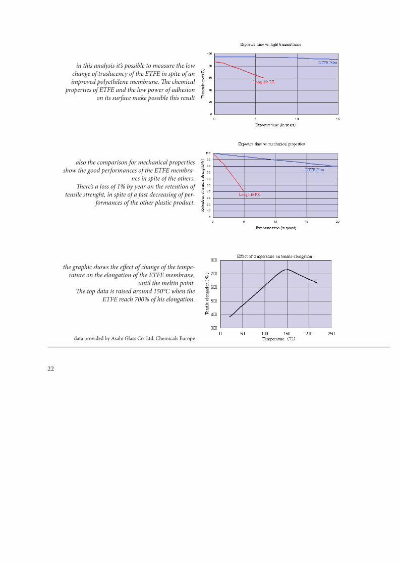
in this analysis it’s possible to measure the low change of traslucency of the ETFE in spite of an improved polyethilene membrane. Th e chemical
properties of ETFE and the low power of adhesion on its surface make possible this result
also the comparison for mechanical properties show the good performances of the ETFE membra-
nes in spite of the others. Th ere’s a loss of 1% by year on the retention of
tensile strenght, in spite of a fast decreasing of per-formances of the other plastic product.
the graphic shows the eff ect of change of the tempe-rature on the elongation of the ETFE membrane,
until the meltin point.Th e top data is raised around 150°C when the
ETFE reach 700% of his elongation.
data provided by Asahi Glass Co. Ltd. Chemicals Europe
23
Projects and use of ETFE
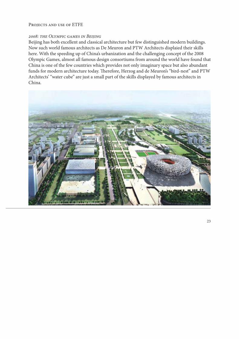
2008: the Olympic games in BeijingBeijing has both excellent and classical architecture but few distinguished modern buildings. Now such world famous architects as De Meuron and PTW Architects displaied their skills here. With the speeding up of China’s urbanization and the challenging concept of the 2008 Olympic Games, almost all famous design consortiums from around the world have found that China is one of the few countries which provides not only imaginary space but also abundant funds for modern architecture today. Th erefore, Herzog and de Meuron’s “bird-nest” and PTW Architects’ “water cube” are just a small part of the skills displayed by famous architects in China.
24
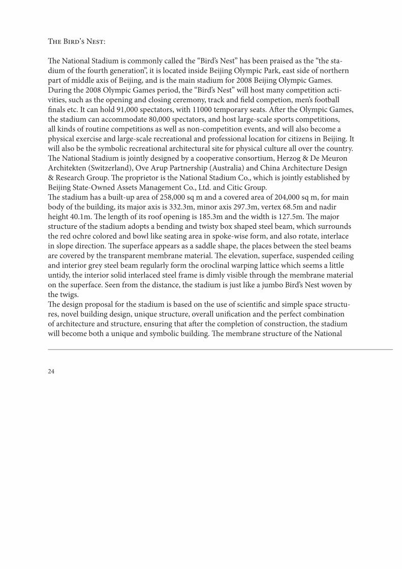
The Bird’s Nest:
Th e National Stadium is commonly called the “Bird’s Nest” has been praised as the “the sta-dium of the fourth generation”, it is located inside Beijing Olympic Park, east side of northern part of middle axis of Beijing, and is the main stadium for 2008 Beijing Olympic Games.During the 2008 Olympic Games period, the “Bird’s Nest” will host many competition acti-vities, such as the opening and closing ceremony, track and fi eld competion, men’s football fi nals etc. It can hold 91,000 spectators, with 11000 temporary seats. Aft er the Olympic Games, the stadium can accommodate 80,000 spectators, and host large-scale sports competitions, all kinds of routine competitions as well as non-competition events, and will also become a physical exercise and large-scale recreational and professional location for citizens in Beijing. It will also be the symbolic recreational architectural site for physical culture all over the country. Th e National Stadium is jointly designed by a cooperative consortium, Herzog & De Meuron Architekten (Switzerland), Ove Arup Partnership (Australia) and China Architecture Design & Research Group. Th e proprietor is the National Stadium Co., which is jointly established by Beijing State-Owned Assets Management Co., Ltd. and Citic Group.Th e stadium has a built-up area of 258,000 sq m and a covered area of 204,000 sq m, for main body of the building, its major axis is 332.3m, minor axis 297.3m, vertex 68.5m and nadir height 40.1m. Th e length of its roof opening is 185.3m and the width is 127.5m. Th e major structure of the stadium adopts a bending and twisty box shaped steel beam, which surrounds the red ochre colored and bowl like seating area in spoke-wise form, and also rotate, interlace in slope direction. Th e superface appears as a saddle shape, the places between the steel beams are covered by the transparent membrane material. Th e elevation, superface, suspended ceiling and interior grey steel beam regularly form the oroclinal warping lattice which seems a little untidy, the interior solid interlaced steel frame is dimly visible through the membrane material on the superface. Seen from the distance, the stadium is just like a jumbo Bird’s Nest woven by the twigs.Th e design proposal for the stadium is based on the use of scientifi c and simple space structu-res, novel building design, unique structure, overall unifi cation and the perfect combination of architecture and structure, ensuring that aft er the completion of construction, the stadium will become both a unique and symbolic building. Th e membrane structure of the National
25
26
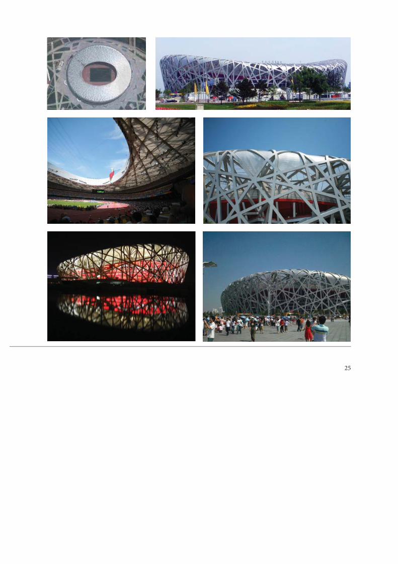
Stadium consists of a roof enclosing structure; acoustics suspended ceiling and internal ring elevation cladding membrane structure three parts. Th e upper chord of roof system adopts single-layer stretching membrane system as maintenance structure of roof for wind and rain resistance and sunlight shading, the transparence ETFE membrane material with the glaze point is selected and disposed on comparatively fl at roof and the adjacent area between the ele-vation and roof. Th e acoustics suspended ceiling of lower chord for roof system adopts white translucence PTFE membrane system as denoise layer and sunlight shading layer at stand area, which is hung beneath the lower chord of main frame and substructure, meanwhile extends downwards from back of upper story stand, functions as screen. Th e elevation of the interior framework of roof opening (internal ring surface) is sealed with PTFE membrane for good waterproofi ng quality. Th e single-layer ETFE stretching membrane structure of roof consists of 1038 membrane units, with total area about 38500m2. On the roof, the drainage gutter is set up along the inside of lattice unit constituted by interwove steel beam, the ETFE membrane unit is fi xed on the border of gutter aft er stretching. Th erefore, the high precision of suppor-ting structure for ETFE membrane unit is essential, because the ETFE membrane unit shape is very complex, especially at shoulder area, where the membrane unit and bracing member should, without exception, be made into complicated hyperboloid form.
27
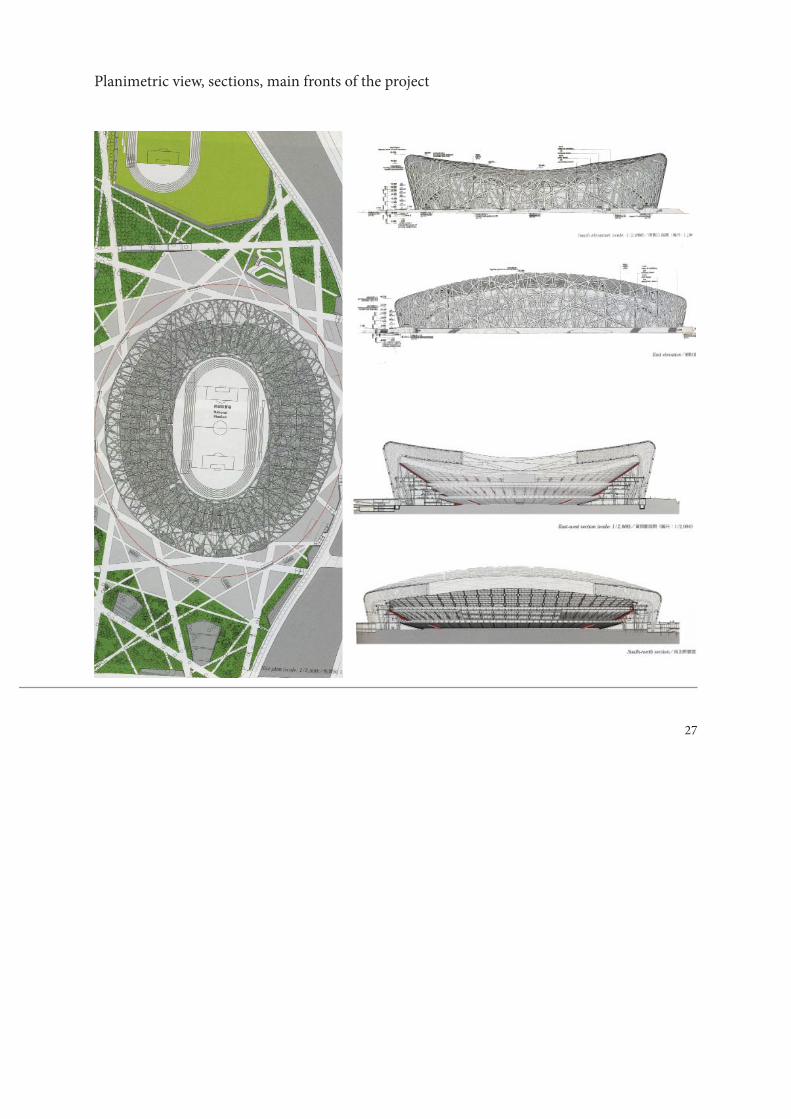
Planimetric view, sections, main fronts of the project
28
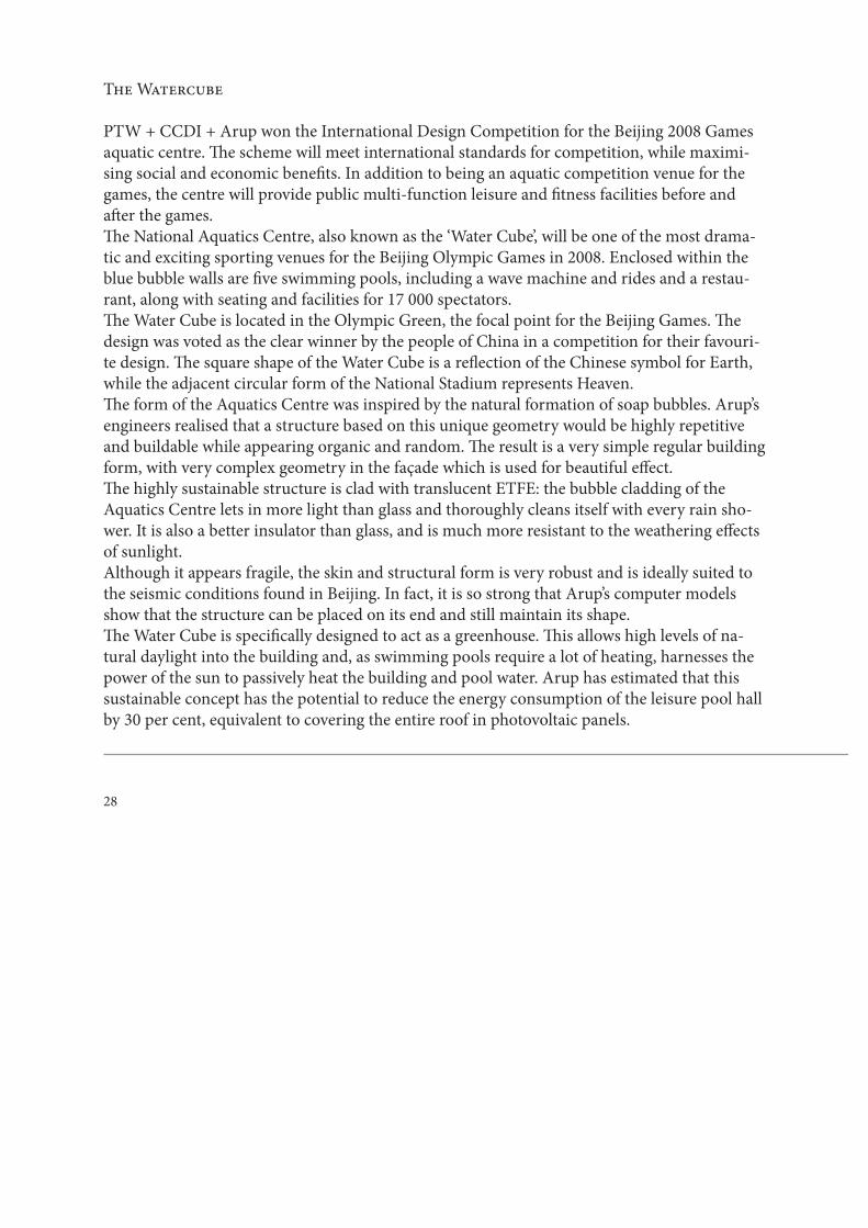
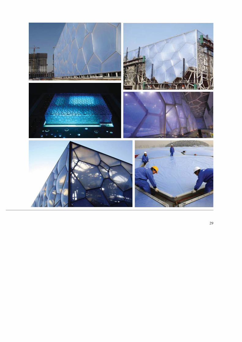
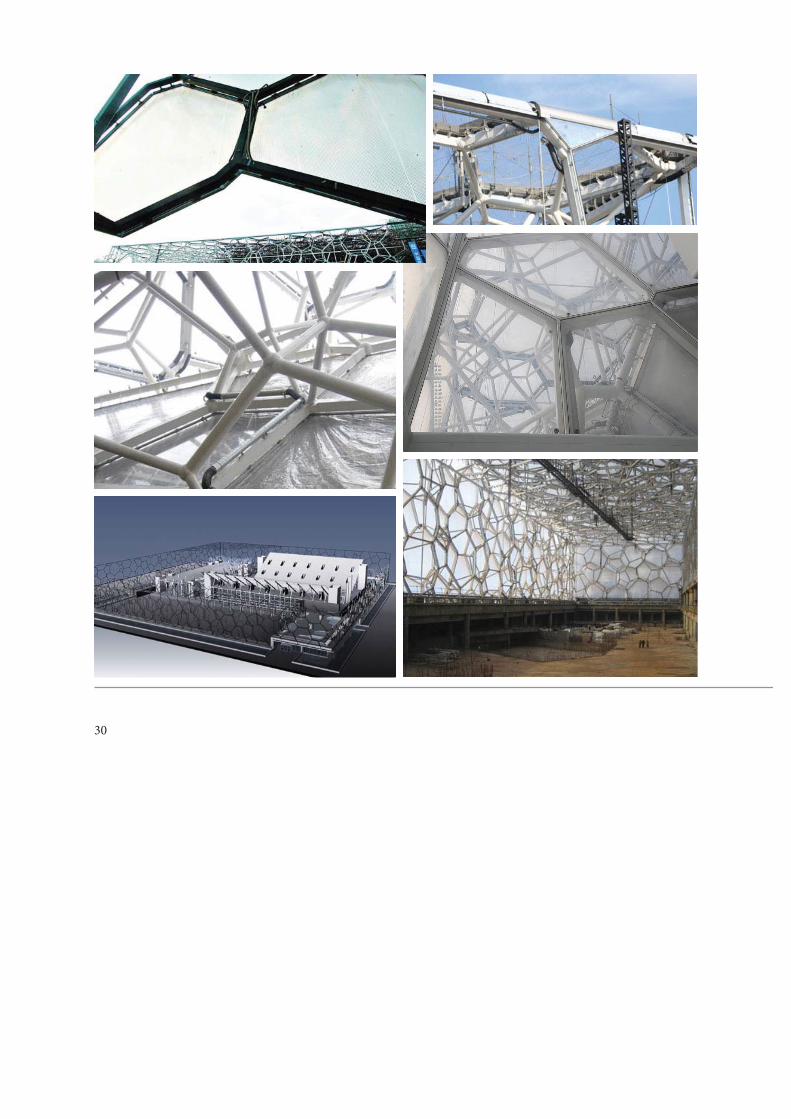
The Watercube
PTW + CCDI + Arup won the International Design Competition for the Beijing 2008 Games aquatic centre. Th e scheme will meet international standards for competition, while maximi-sing social and economic benefi ts. In addition to being an aquatic competition venue for the games, the centre will provide public multi-function leisure and fi tness facilities before and aft er the games.Th e National Aquatics Centre, also known as the ‘Water Cube’, will be one of the most drama-tic and exciting sporting venues for the Beijing Olympic Games in 2008. Enclosed within the blue bubble walls are fi ve swimming pools, including a wave machine and rides and a restau-rant, along with seating and facilities for 17 000 spectators.Th e Water Cube is located in the Olympic Green, the focal point for the Beijing Games. Th e design was voted as the clear winner by the people of China in a competition for their favouri-te design. Th e square shape of the Water Cube is a refl ection of the Chinese symbol for Earth, while the adjacent circular form of the National Stadium represents Heaven.Th e form of the Aquatics Centre was inspired by the natural formation of soap bubbles. Arup’s engineers realised that a structure based on this unique geometry would be highly repetitive and buildable while appearing organic and random. Th e result is a very simple regular building form, with very complex geometry in the façade which is used for beautiful eff ect.Th e highly sustainable structure is clad with translucent ETFE: the bubble cladding of the Aquatics Centre lets in more light than glass and thoroughly cleans itself with every rain sho-wer. It is also a better insulator than glass, and is much more resistant to the weathering eff ects of sunlight.Although it appears fragile, the skin and structural form is very robust and is ideally suited to the seismic conditions found in Beijing. In fact, it is so strong that Arup’s computer models show that the structure can be placed on its end and still maintain its shape.Th e Water Cube is specifi cally designed to act as a greenhouse. Th is allows high levels of na-tural daylight into the building and, as swimming pools require a lot of heating, harnesses the power of the sun to passively heat the building and pool water. Arup has estimated that this sustainable concept has the potential to reduce the energy consumption of the leisure pool hall by 30 per cent, equivalent to covering the entire roof in photovoltaic panels.
29
30
31
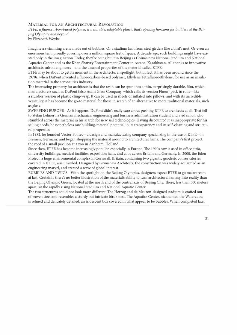
Material for an Architectural RevolutionETFE, a fl uorocarbon-based polymer, is a durable, adaptable plastic that’s opening horizons for builders at the Bei-jing Olympics and beyondby Elizabeth Woyke
Imagine a swimming arena made out of bubbles. Or a stadium knit from steel girders like a bird’s nest. Or even an enormous tent, proudly covering over a million square feet of space. A decade ago, such buildings might have exi-sted only in the imagination. Today, they’re being built in Beijing as China’s new National Stadium and National Aquatics Center and as the Khan Shatyry Entertainment Center in Astana, Kazakhstan. All thanks to innovative architects, adroit engineers—and the unusual properties of the material called ETFE.ETFE may be about to get its moment in the architectural spotlight, but in fact, it has been around since the 1970s, when DuPont invented a fl uorocarbon-based polymer, Ethylene Tetrafl uoroethylene, for use as an insula-tion material in the aeronautics industry.Th e interesting property for architects is that the resin can be spun into a thin, surprisingly durable, fi lm, which manufacturers such as DuPont (also Asahi Glass Company, which calls its version Fluon) pack in rolls—like a sturdier version of plastic cling-wrap. It can be used in sheets or infl ated into pillows, and with its incredible versatility, it has become the go-to material for those in search of an alternative to more traditional materials, such as glass.SWEEPING EUROPE - As it happens, DuPont didn’t really care about pushing ETFE to architects at all. Th at fell to Stefan Lehnert, a German mechanical engineering and business administration student and avid sailor, who stumbled across the material in his search for new sail technologies. Having discounted it as inappropriate for his sailing needs, he nonetheless saw building-material potential in its transparency and its self-cleaning and structu-ral properties.In 1982, he founded Vector Foiltec—a design and manufacturing company specializing in the use of ETFE—in Bremen, Germany, and began shopping the material around to architectural fi rms. Th e company’s fi rst project, the roof of a small pavilion at a zoo in Arnheim, Holland.Since then, ETFE has become increasingly popular, especially in Europe. Th e 1990s saw it used in offi ce atria, university buildings, medical facilities, exposition halls, and zoos across Britain and Germany. In 2000, the Eden Project, a huge environmental complex in Cornwall, Britain, containing two gigantic geodesic conservatories covered in ETFE, was unveiled. Designed by Grimshaw Architects, the construction was widely acclaimed as an engineering marvel, and created a wave of global interest.BUBBLES AND TWIGS - With the spotlight on the Beijing Olympics, designers expect ETFE to go mainstream at last. Certainly there’s no better illustration of the material’s ability to turn architectural fantasy into reality than the Beijing Olympic Green, located at the north end of the central axis of Beijing City. Th ere, less than 500 meters apart, sit the rapidly rising National Stadium and National Aquatic Center.Th e two structures could not look more diff erent. Th e Herzog and de Meuron-designed stadium is craft ed out of woven steel and resembles a sturdy but intricate bird’s nest. Th e Aquatics Center, nicknamed the Watercube, is refi ned and delicately detailed, an iridescent box covered in what appear to be bubbles. When completed later
32
this year, both will showcase innovative uses of ETFE. To protect spectators from rain and wind, the stadium will feature red ETFE cushions inserted in the spaces between the “twigs” of its “nest.” Th e 750,000 square foot Water-cube, the largest ETFE project ever, will be clad entirely (roof and four walls) in blue ETFE cushions.Given the extensive size and expense (an estimated $100 million) of the Watercube project, it’s surprising to note that this will be the fi rst time that Sydney, Australia’s PTW Architects have actually used the fabric. Th ey’re that confi dent. John Bilmon, managing director at the company, says they chose ETFE over glass and fi berglass because it satisfi ed the project’s engineering needs. Some bubbles in the design span 30 feet without any internal framing—a distance that wouldn’t be possible with other materials.NO SHARP OBJECTS - But the ETFE system also cost less (though they wouldn’t give specifi cs) than an equiva-lent traditional system, freeing up money for higher-quality fi ltration and water-treatment systems for the center’s pools. A more traditional form of cladding would have been not only more expensive and cumbersome, says Bilmon, it would have resulted in a “…less exciting, beautiful, and functional building.”Th e material’s appeal is manifold, and those who work with it praise its unique properties. First, it’s extremely light—about 1/100 the weight of glass—and deceptively strong, able to stretch to three times its length without losing its elasticity. (Having said that, a sharp implement like a knife can puncture it—one reason it’s used mostly for roofs.)If the fi lm does tear, it can be patched with other pieces of ETFE. When exposed to fi re, it soft ens and shrinks away from the heat, naturally venting smoke out of a building. And it’s naturally nonstick, nonporous surface, which has chemical properties similar to DuPont’s other best-selling material, Tefl on, is so slick that dirt, snow, and rain simply slide off .SHAPE SHIFTER - Its light weight reduces corresponding structural costs. Edward Peck, managing director of the North American Division of Foiltec, which now has 12 offi ces and 250 employees worldwide, estimates that a simple, small roofi ng project could be 10% cheaper if ETFE were used. For larger, more complicated projects, the overall construction savings could reach 60%.Th en there’s the fun factor. ETFE comes in diff erent fi nishes (transparent, matte) and colors, and can be lit from within using LED lights or decorated with light projections like a giant movie screen. It can be printed with patterns by running it through a special press—something not possible with glass. It can take myriad shapes, too: Strips can be heat-welded together like fabric squares in a quilt. Th is “sewing” method enables ETFE to be instal-led in pieces much longer and wider than glass. A large glass panel might measure 10 ft . by 5 ft ., whereas a strip of ETFE could be 180 feet long and 12 feet wide, with structural supports.It also scores well on the environmentally friendly front, particularly crucial given the current call for greener building practices. Th e fi lm is recyclable (simply melt and reuse), and due to its light weight, doesn’t require much energy to transport. Th e Watercube is designed to gather heat passing through its ETFE walls and roof—energy that can be used to heat the building’s water systems or expelled through vents if the building gets too hot.HIGH MAINTENANCE - On an aesthetic level, the cushions reinforce the building’s theme. Th eir pillowy shapes evoke a bubbles’s roundness, and their triple-layered construction, which mixes layers of blue fi lm with transpa-rent fi lm, gives the façade a sense of depth and shift ing color. Once the games start in August, 2008, offi cials will be able to transform the walls into a giant TV screen showing simultaneous projections of the swimming activi-
33
ties taking place inside.For all its wondrous properties, ETFE isn’t an entirely perfect material. In its typical usage, two or three layers are welded together and shipped fl at to the job site, where they’re infl ated into panels or “cushions”. Th ese cushions require semi-continuous air pressure—to keep them stable and give them thermal properties—so most systems include thin hoses that plug into the cushions’ sides.Th ese air-supply lines connect to a computerized system that monitors the pressure within the cushions. Th is system can also feed air into, or eject air from, particular chambers or layers to let in more light or create more shade, meaning the ETFE cushions act as a dynamic puff er jacket for buildings. In some installations, this is done automatically using light sensors.OVERHEARD OVERHEAD - Of course, many projects don’t call for such complexity. “You have to evaluate, project by project, what the driving force is for using ETFE,” says Foiltec’s Peck. “Is it for architectural imagery, for transparency, for structural reasons or thermal performance?” He doesn’t advise using it for small-scale or residential projects.Acoustics can be another drawback. Th e cushion system, when used on a roof, can amplify the sound of rain because the tension in the cushion acts like a drum. Manufacturers have developed several noise-suppressing techniques, including layering polycarbonate sheets within ETFE cushions, but their use isn’t widespread yet.Interior applications, such as walls within an offi ce, present other sound issues. ETFE transmits more sound than glass or wood, making it ill-suited for meeting rooms or conference centers near airports, to name one ETFE proposal that was quashed by noise concerns. Conversely, ETFE can be benefi cial for self-contained, noisy areas like aquatic parks—sound bounces off the walls and fl oor and escapes through the roof.JUST THE BEGINNING - But plans are already under way to address these concerns, and ETFE is already crop-ping up in more and more locations. Foiltec has eight projects that will be built in the U.S. next year (and more than 100 projects slated worldwide), and has just completed an atrium roof for a U.S. Federal building. Peck hopes the latter project might prove to be a turning point for ETFE in the U.S., which has been notably slow to catch on to the material’s potential. ETFE was named in three of the four submissions for the Beijing National Aquatic Center, and can be seen in several proposals for the 2012 London Olympics.Another large ETFE project is already on the horizon: Th e Khan Shatyry Entertainment Center, a 1,076,000-sq.-ft . tent-shaped recreational complex in the capital of Kazakhstan, designed by London fi rm Foster + Partners is due for completion next year. Other top-tier architecture fi rms, like Skidmore, Owings & Merrill (SOM) and Gehry Partners, are said to be considering ETFE for upcoming projects.And other innovations are still being developed. Foiltec is currently testing whether it might be possible to attach photovoltaics to ETFE panels or use an insulating “nanogel” to increase a panel’s thermal properties. As Bilmon, the Watercube architect, says: “Th ere’s a new realization that the whole of the world is facing sustainability is-sues—and solutions like ETFE are required for the future.”
business week - April 24, 2007
34
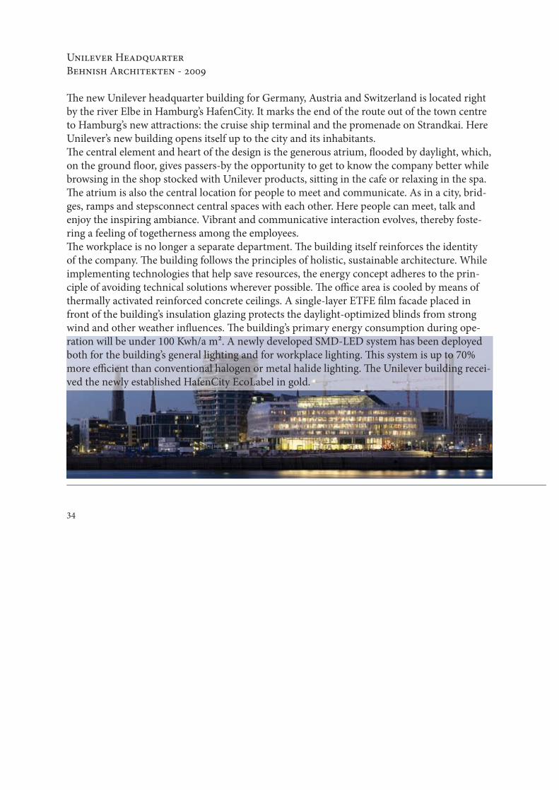
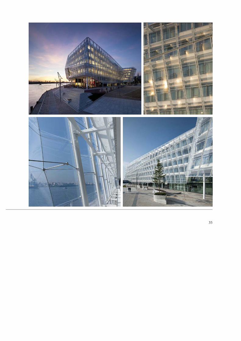
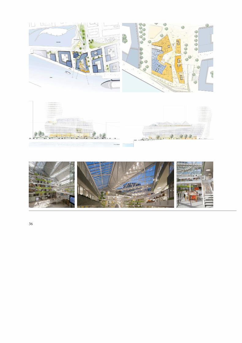
Unilever HeadquarterBehnish Architekten - 2009
Th e new Unilever headquarter building for Germany, Austria and Switzerland is located right by the river Elbe in Hamburg’s HafenCity. It marks the end of the route out of the town centre to Hamburg’s new attractions: the cruise ship terminal and the promenade on Strandkai. Here Unilever’s new building opens itself up to the city and its inhabitants. Th e central element and heart of the design is the generous atrium, fl ooded by daylight, which, on the ground fl oor, gives passers-by the opportunity to get to know the company better while browsing in the shop stocked with Unilever products, sitting in the cafe or relaxing in the spa. Th e atrium is also the central location for people to meet and communicate. As in a city, brid-ges, ramps and stepsconnect central spaces with each other. Here people can meet, talk and enjoy the inspiring ambiance. Vibrant and communicative interaction evolves, thereby foste-ring a feeling of togetherness among the employees. Th e workplace is no longer a separate department. Th e building itself reinforces the identity of the company. Th e building follows the principles of holistic, sustainable architecture. While implementing technologies that help save resources, the energy concept adheres to the prin-ciple of avoiding technical solutions wherever possible. Th e offi ce area is cooled by means of thermally activated reinforced concrete ceilings. A single-layer ETFE fi lm facade placed in front of the building’s insulation glazing protects the daylight-optimized blinds from strong wind and other weather infl uences. Th e building’s primary energy consumption during ope-ration will be under 100 Kwh/a m². A newly developed SMD-LED system has been deployed both for the building’s general lighting and for workplace lighting. Th is system is up to 70% more effi cient than conventional halogen or metal halide lighting. Th e Unilever building recei-ved the newly established HafenCity EcoLabel in gold.
35
36
37
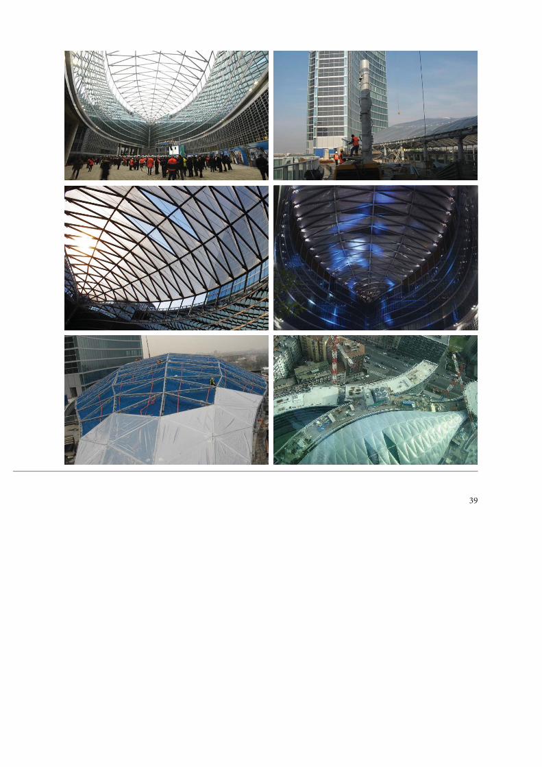
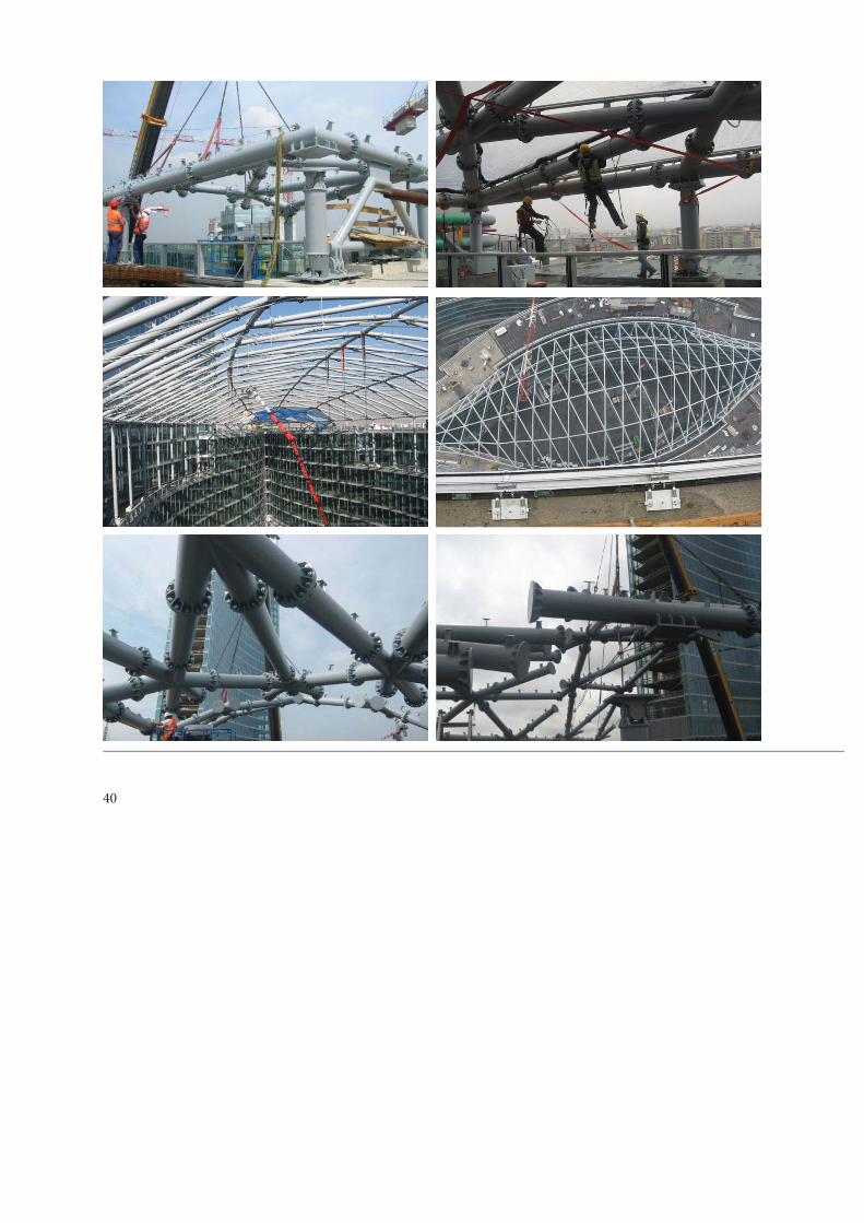
Palazzo LombardiaPei Cobb Freed & Partners - 2007
Th is is the winning entry in an international design competition for the Lombardy Regional Government’s New Seat and civic square, required to have a visible symbolic and functional presence. Signifi cant to the design is its integration with the Pirelli Tower, which houses related regional government offi ces, with the urban context of Milan and with the Lombardy region. Sited in the greater Garibaldi-Repubblica urban enhancement area, close to the heart of the city, its scale relates to the surrounding neighborhood, while the tower speaks to the Pirelli building and the city. Key design principles are: - an urban passage invites entry. - it is a signifi cant destination. - there is a sequence of engaging spaces. - animated edges give shape to public space. - the design promotes social interaction. - an emblematic vertical element contributes to Milan’s skyline. Th e building’s sinuous interweaving strands recall the mountains, valleys, and rivers of the region. Th eir curvilinear forms are adaptable to changing functional requirements and are receptive to the region’s evolving organizational structure. In addition to its headquarter functions, the building accommodates public amenities accessible to all. Th e central piazza, projected with curved glass roof, but realized in ETFE, recalls Milan’s Galleria while linking to two secondary open spaces and a linear landscaped spine, together celebrating the natural environment, rich culture, and citizens of Lombardy.Th e cover of the plaza, 3. 380 sq.m. of developement, presents a typical structural system used for glass, so it’s more than hyperstatic for the ETFE, but the constructor prefer to mantain the original design of the architect to built this roof, the fi rst time projected with a glass system. Th e change of materials had to be necessary for the weight of the glass panels, so the choice to contact Vector Foiltec to install ETFE, 10 times lighter than glass.
38
39
40
41
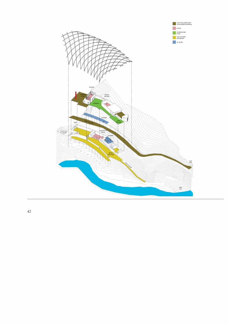
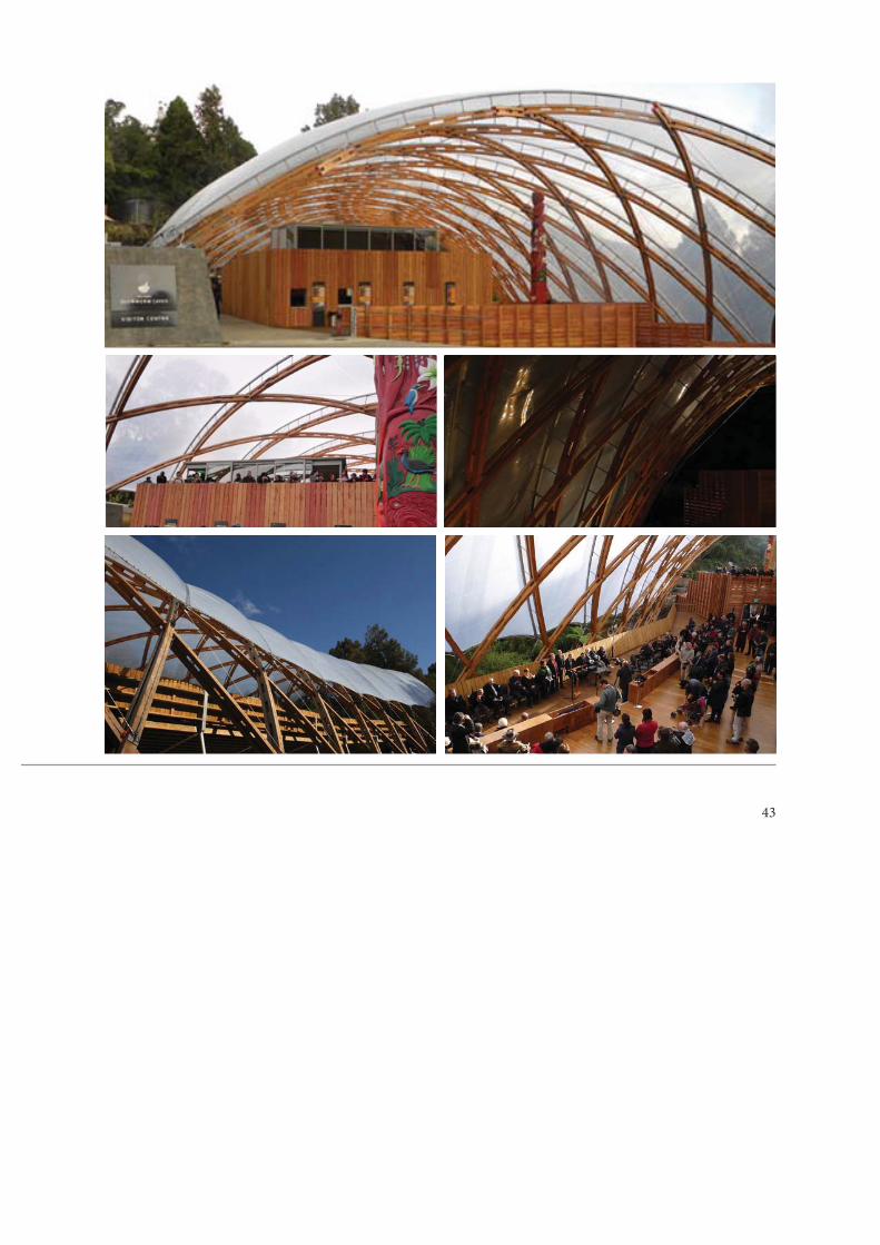
New Waitomo Caves Visitor CentreArchitecture Workshop - 2010
Sheltered below an innovative woven timber canopy, new amenities for visitors to the Waitomo Caves includes tourist gathering areas, a 250-seat dining, retail, seminar and exhibition areas as well as a café and theatre for Tourism Holdings Ltd. Th e cave entrance is accessed from the car park on the upper path while a lower path returns the visitors back alongside the stream exit. Between these paths the amenities were accommo-dated within a simple base structure that extended the contours of the land. Th e form of the base is distinguished and separate from the curved geometry of the overhead canopy.Th e historic caves were formed from the limestone transported by water over thousands of years, so we wanted to emphasis a connection with the Waitomo stream and the fl ows of water running through the caves. Th e canopy gridshell is aligned with the curve of the Waitomo stream. It reinforces the generating idea for this project of a simple lightweight ‘sky shell’ to counterpoint the subterranean cave space that is dissolved and molded out of the ground. Th e canopy in combination with the caves, create a positive and a negative, if you like. Th e structure of the centre is internationally signifi cant. Th e geometry of the canopy was de-scribed by the surface of a toroid and Radiata pine LVL (laminated veneer lumber) was pre-fabricated into curved (and twisted) ribs in Hunter’s factory in Nelson. Th ese timber I-beams were joined, overlapped in layers, then screwed together as they were assembled on site by Hawkins Construction. Th e weaving of the timber structure to create a timber net or ‘gridshell’ is recalled by the local hapu as a hinaki or Maori eel trap. Th e gridshell was calculated by Ali-stair Cattanach at Dunning Th ornton Consultants. His analysis was peer reviewed in London by Happold Structural Engineers, who commented favourably on the strengths achieved with NZ pine LVL and an innovative soft pad connection with the over cladding. Infl ated ETFE air pillows were tethered over the gridshell structure like a tent fl y. Th e long translucent pillows are structurally effi cient in spans of 4-5m and followed the lines of the LVL ribs. Th e gridshell was designed to span across the existing pathways and provide some shelter in the journey to and from the caves as well as maintain a strong connection to the established Kahikatea bush.
42
caveexit
wc facility
wc facility
caveentry
dining(200 seat)
ticketing& info
theatre(45 seat)
exhibition
wc facility
cave entry path/musterarrival platform/ticketing
events
cafe(60 seat)
cave exit pathdining/retail
exhibition/cafeevent
tunnel exitto carpark
retail
cave exit path
cave entry path
meeting
conference/dining
43

THIN
PHOTOVOLTAIC
FILMS
46
Analysis of the technologies
Photovoltaic conversion of solar energy is based on semiconductor electronics. Although materials such as GaAs, CulnSe2 and CdTe may be without any doubt valid alternatives, still today the photovoltaic market is by far dominated by silicon. About 80% of the solar-cell world PV production for terrestrial applications has its origin in mono-crystalline (c-Si) and multi-crystalline silicon (mc-Si) wafer technology. Most of the remaining 20% market is dominated by thin-silicon (amorphous, microcrystalline, nanocrystalline, etc.) and by hybrid amorphous-crystalline solar cells (a-Si, μc-Si). Experience has induced the conviction that silicon technology must dominate the PV market for the next 10 years: the cause of this predominant position is the combination of a number of factors, such as the maturity of silicon PV technologies, the good and well-known optoelectro-nic properties of the material, its availability, lack of toxicity, cost, chemical stability, etc. During 2001 a total supply of 26 000 tons of silicon reached the electronic industry, of which around 15% were used to supply the PV market. Europe is a leader in the production of crystalline ingots and wafers for PV applications, in particular in Germany where are concen-trated a large number of these industries and also branches of big international groups. Crystalline-silicon (c-Si) wafer-based technology must evolve towards lower costs by imple-menting new material-fabrication processes and making wafers thinner. On the other hand, silicon grown directly on low cost substrates is forced to progress in the direction of improving the optoelectronic properties of the material and its growth rate and consistently of making the cell active-layer thicker. Several eff orts have been done since 1994 based on European projects dealt with diff erent options concerning substrates (silicon ribbons, conductive and insulating ceramics) and deposition technologies (high- temperature chemical vapour deposition - CVD) and solution growth-SG: the consequence of all this is a clear convergence of two families of research lines based the fi rst on wafers, the other on the growth of silicon onto low-cost sub-strates that have traditionally progressed quite independently. Synergy can come out of this mutual approximation, and may be the origin of important advances in next generation PV.For a long while, wafer and thin-fi lm technologies have evolved as competing options, as if the solutions to the technical problems could have come out from only one of these two research lines. In the last few years, however, new possibilities have arisen on the basis of a number of
47
technological approaches for the fabrication of inexpensive multi-crystalline silicon, for the growth of poly-crystalline silicon thin fi lms on inexpensive substrates or for the deposition of high-quality microcrystalline-silicon thin fi lms at competitive growth rates.
Present research lines in europe
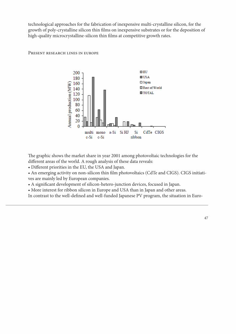
Th e graphic shows the market share in year 2001 among photovoltaic technologies for the diff erent areas of the world. A rough analysis of these data reveals:• Diff erent priorities in the EU, the USA and Japan. • An emerging activity on non-silicon thin fi lm photovoltaics (CdTe and CIGS). CIGS initiati-ves are mainly led by European companies.• A signifi cant development of silicon-hetero-junction devices, focused in Japan.• More interest for ribbon silicon in Europe and USA than in Japan and other areas.In contrast to the well-defi ned and well-funded Japanese PV program, the situation in Euro-
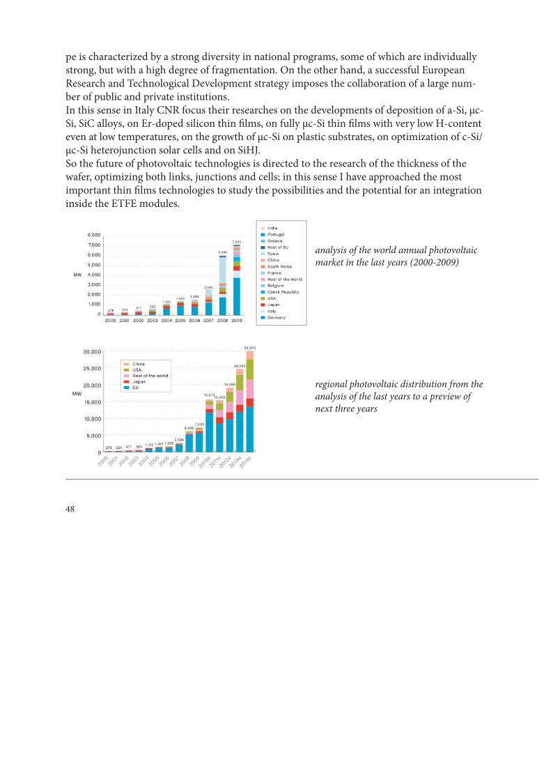
48
pe is characterized by a strong diversity in national programs, some of which are individually strong, but with a high degree of fragmentation. On the other hand, a successful European Research and Technological Development strategy imposes the collaboration of a large num-ber of public and private institutions.In this sense in Italy CNR focus their researches on the developments of deposition of a-Si, μc-Si, SiC alloys, on Er-doped silicon thin fi lms, on fully μc-Si thin fi lms with very low H-content even at low temperatures, on the growth of μc-Si on plastic substrates, on optimization of c-Si/μc-Si heterojunction solar cells and on SiHJ.So the future of photovoltaic technologies is directed to the research of the thickness of the wafer, optimizing both links, junctions and cells; in this sense I have approached the most important thin fi lms technologies to study the possibilities and the potential for an integration inside the ETFE modules.
analysis of the world annual photovoltaic market in the last years (2000-2009)
regional photovoltaic distribution from the analysis of the last years to a preview of next three years
49
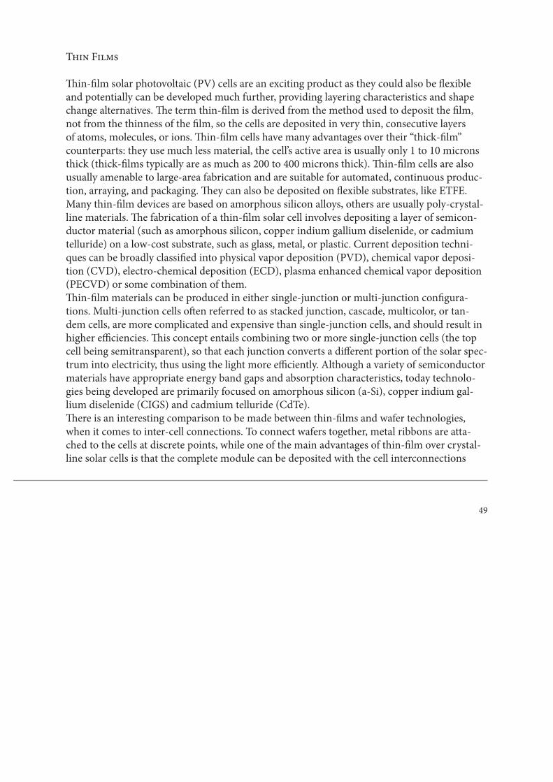
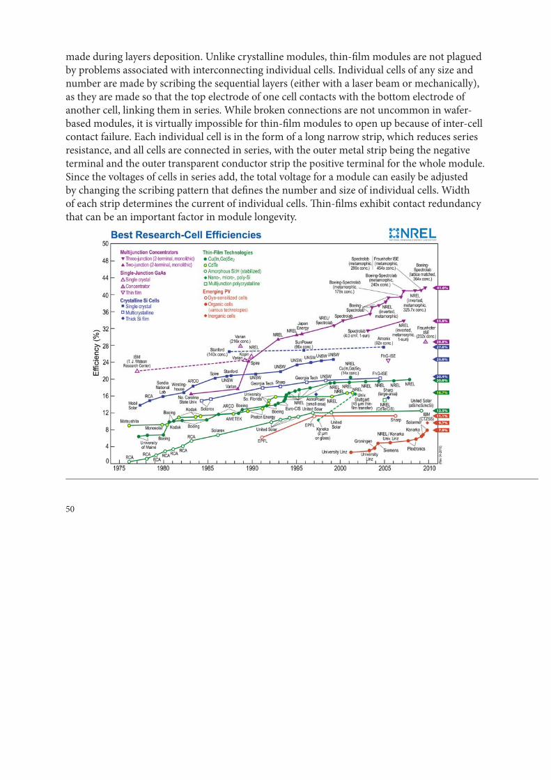
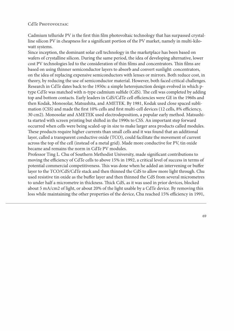
Thin Films
Th in-fi lm solar photovoltaic (PV) cells are an exciting product as they could also be fl exible and potentially can be developed much further, providing layering characteristics and shape change alternatives. Th e term thin-fi lm is derived from the method used to deposit the fi lm, not from the thinness of the fi lm, so the cells are deposited in very thin, consecutive layers of atoms, molecules, or ions. Th in-fi lm cells have many advantages over their “thick-fi lm” counterparts: they use much less material, the cell’s active area is usually only 1 to 10 microns thick (thick-fi lms typically are as much as 200 to 400 microns thick). Th in-fi lm cells are also usually amenable to large-area fabrication and are suitable for automated, continuous produc-tion, arraying, and packaging. Th ey can also be deposited on fl exible substrates, like ETFE.Many thin-fi lm devices are based on amorphous silicon alloys, others are usually poly-crystal-line materials. Th e fabrication of a thin-fi lm solar cell involves depositing a layer of semicon-ductor material (such as amorphous silicon, copper indium gallium diselenide, or cadmium telluride) on a low-cost substrate, such as glass, metal, or plastic. Current deposition techni-ques can be broadly classifi ed into physical vapor deposition (PVD), chemical vapor deposi-tion (CVD), electro-chemical deposition (ECD), plasma enhanced chemical vapor deposition (PECVD) or some combination of them.Th in-fi lm materials can be produced in either single-junction or multi-junction confi gura-tions. Multi-junction cells oft en referred to as stacked junction, cascade, multicolor, or tan-dem cells, are more complicated and expensive than single-junction cells, and should result in higher effi ciencies. Th is concept entails combining two or more single-junction cells (the top cell being semitransparent), so that each junction converts a diff erent portion of the solar spec-trum into electricity, thus using the light more effi ciently. Although a variety of semiconductor materials have appropriate energy band gaps and absorption characteristics, today technolo-gies being developed are primarily focused on amorphous silicon (a-Si), copper indium gal-lium diselenide (CIGS) and cadmium telluride (CdTe).Th ere is an interesting comparison to be made between thin-fi lms and wafer technologies, when it comes to inter-cell connections. To connect wafers together, metal ribbons are atta-ched to the cells at discrete points, while one of the main advantages of thin-fi lm over crystal-line solar cells is that the complete module can be deposited with the cell interconnections
50
made during layers deposition. Unlike crystalline modules, thin-fi lm modules are not plagued by problems associated with interconnecting individual cells. Individual cells of any size and number are made by scribing the sequential layers (either with a laser beam or mechanically), as they are made so that the top electrode of one cell contacts with the bottom electrode of another cell, linking them in series. While broken connections are not uncommon in wafer-based modules, it is virtually impossible for thin-fi lm modules to open up because of inter-cell contact failure. Each individual cell is in the form of a long narrow strip, which reduces series resistance, and all cells are connected in series, with the outer metal strip being the negative terminal and the outer transparent conductor strip the positive terminal for the whole module. Since the voltages of cells in series add, the total voltage for a module can easily be adjusted by changing the scribing pattern that defi nes the number and size of individual cells. Width of each strip determines the current of individual cells. Th in-fi lms exhibit contact redundancy that can be an important factor in module longevity.
51
Amorphous silicon
HistoryTh e last quarter century witnessed the birth, the adolescence, and the maturity of amorphous silicon (a-Si) based photovoltaic (PV) technology. As it usher in the twenty-fi rst century, it must also meet the ever increasing energy demand while addressing environmental issues and ecological concerns. Th e a-Si PV technology has positioned itself as the low-cost solution to the challenge of energy, environmental, and ecology (the e-tripos).As the a-Si photovoltaic industry still experiences unavoidable growing pains, large-volume manufacturing plants are ready to demonstrate their competiveness in the rapidly growing glo-bal market. Photovoltaics in general, and a-Si technology in particular, will undoubtedly play a signifi cant role in providing clean, quiet, and renewable energy harvested from the inexhau-stible sun. Th e volume of worldwide sales of a-Si modules was 34 MW in 2001, a phenomenal growth of 26% over the previous year, but only represents less than 10% of the total photovol-taic market. In the next quarter century, the most important brands expect the a-Si technology will attain a greater share of the world market. In recent years, the feasibility of using a-Si PV for space applications has been investigated due to its high specifi c power (W/kg) and low cost. Nineteen months of experience on board MIR Space Station has revolutionarily uplift ed the outlook for use of a-Si solar arrays for future mis-sions in space. Th e a-Si photovoltaic has been identifi ed as the enabling technology for certain applications.
Analysis and advantagesLow cost is one of the leading advantages of a-Si photovoltaic modules. Two of the major ingredients of the a-Si alloy are silicon and hydrogen. Th ey are environmentally friendly and abundant on earth. Furthermore, a-Si alloys are characterized by a high absorption coeffi cient. Only a thin fi lm (< 1 μ m) is needed to absorb the sunlight, and this leads to low material cost. Good conversion effi ciency is another advantage for a-Si modules. In the laboratory, it’s used the radio-frequency plasma-enhanced chemical vapor deposition method and it has been de-monstrated a stable cell effi ciency of 13% using a spectrum splitting triple-junction structure. In addition, low cost manufacturing is also an important requirement.
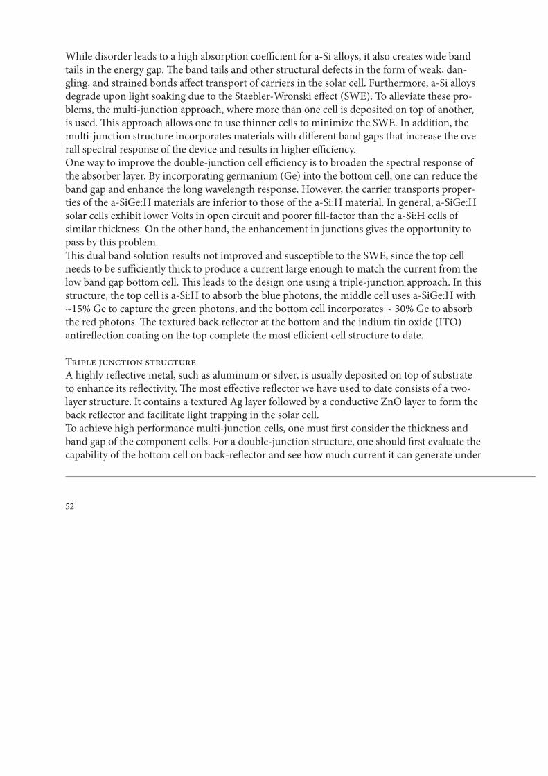
52
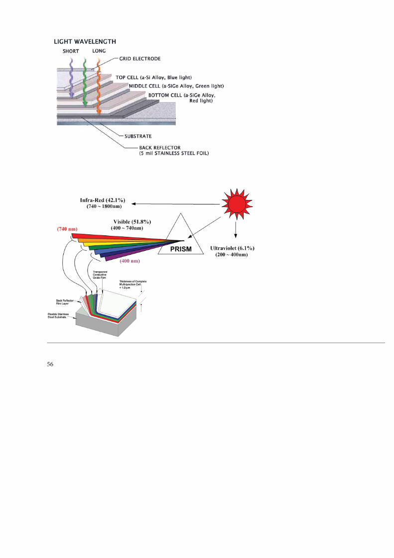
While disorder leads to a high absorption coeffi cient for a-Si alloys, it also creates wide band tails in the energy gap. Th e band tails and other structural defects in the form of weak, dan-gling, and strained bonds aff ect transport of carriers in the solar cell. Furthermore, a-Si alloys degrade upon light soaking due to the Staebler-Wronski eff ect (SWE). To alleviate these pro-blems, the multi-junction approach, where more than one cell is deposited on top of another, is used. Th is approach allows one to use thinner cells to minimize the SWE. In addition, the multi-junction structure incorporates materials with diff erent band gaps that increase the ove-rall spectral response of the device and results in higher effi ciency. One way to improve the double-junction cell effi ciency is to broaden the spectral response of the absorber layer. By incorporating germanium (Ge) into the bottom cell, one can reduce the band gap and enhance the long wavelength response. However, the carrier transports proper-ties of the a-SiGe:H materials are inferior to those of the a-Si:H material. In general, a-SiGe:H solar cells exhibit lower Volts in open circuit and poorer fi ll-factor than the a-Si:H cells of similar thickness. On the other hand, the enhancement in junctions gives the opportunity to pass by this problem.Th is dual band solution results not improved and susceptible to the SWE, since the top cell needs to be suffi ciently thick to produce a current large enough to match the current from the low band gap bottom cell. Th is leads to the design one using a triple-junction approach. In this structure, the top cell is a-Si:H to absorb the blue photons, the middle cell uses a-SiGe:H with ~15% Ge to capture the green photons, and the bottom cell incorporates ~ 30% Ge to absorb the red photons. Th e textured back refl ector at the bottom and the indium tin oxide (ITO) antirefl ection coating on the top complete the most effi cient cell structure to date.
Triple junction structureA highly refl ective metal, such as aluminum or silver, is usually deposited on top of substrate to enhance its refl ectivity. Th e most eff ective refl ector we have used to date consists of a two-layer structure. It contains a textured Ag layer followed by a conductive ZnO layer to form the back refl ector and facilitate light trapping in the solar cell. To achieve high performance multi-junction cells, one must fi rst consider the thickness and band gap of the component cells. For a double-junction structure, one should fi rst evaluate the capability of the bottom cell on back-refl ector and see how much current it can generate under
53
the standard spectrum. Th e rule of thumb is then to design the top cell to produce about half the current. During the optimization process, it is oft en useful to evaluate the bottom cell with a red fi lter to simulate its operation in a double-junction structure. Since the top cell usually uses a-Si:H and shows a good fi ll factor due to its small thickness and superior material quality, it is benefi cial to slightly limit the double-junction current by the top cell. It is also important to keep in mind that the desired amount of current mismatch should be determined by the degradation behavior of the component cells aft er light soaking. A similar approach can be ap-plied to the triple-junction structure. One should fi rst evaluate the bottom cell on back refl ec-tor. Th e top cell should roughly produce one-third of the bottom-cell current, and the middle cell two thirds. Again, it is useful to evaluate the middle and bottom cells with appropriate fi lters to simulate their operations in a triple-junction structure.Th e doped layers that fl ank the i layers are necessary for solar cell operations, but they are not photovoltaically active. Th ey represent parasitic loss both electrically and optically. Th e p layer through which the light enters the solar cell is particularly important and should be as transpa-rent and conductive as possible.
54
Uni-Solar, leader in triple junction technology, has developed a microcrystalline p layer, which resulted in a signifi cant improvement in the cell performance. In a multi-junction structure, a tunnel-junction is formed consisting of the two adjacent doped layers of the two adjacent com-ponent cells. Because the tunnel junction consists of thin doped layers, carriers can be conside-red to ‘tunnel’ through the layers. In reality, photogenerated electrons and holes recombine in the ‘tunnel’ junction. Th us, it is also referred to as the ‘recombination’ junction. However, the polarity of the tunnel junction is opposite to that of the multi-junction device. It is therefore important to minimize losses associated with the tunnel-junction. Th e quality of the component cells determines the performance of the multi-junction structu-re. Th e component cells are the basic building blocks. It is convenient to evaluate and optimize each component cell separately, then integrate them into a multi-junction confi guration. It is useful to evaluate the component cells under appropriate illumination conditions correspon-ding to their respective spectral response in a multi-junction structure. I should point out that high quality component cells are necessary but not suffi cient conditions for achieving high effi ciencies. Th is is analogous to the fact that high quality intrinsic material is a necessary but not suffi cient condition for fabricating high effi ciency solar cells.
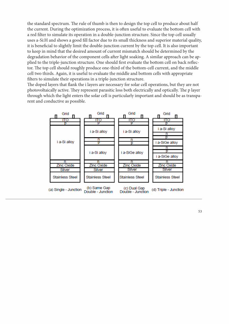
the eff ect of the Ag/ZnO conductive layer on the effi cency of the cell
the eff ect of the triple junction spectrum: the catch in the three layers of diff erent wavelenghts optimze the effi ciency of the whole cell
55
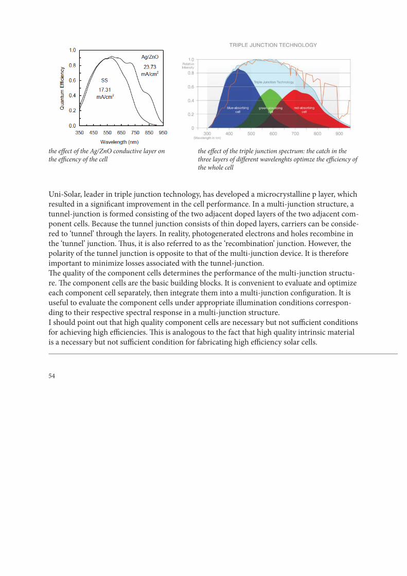
A key feature in the manufacturing technology for the production of the amorphous silicon cells is the roll-to-roll continuous deposition process. Only fl exible substrates are compatible with this process. A roll of 0,12mm thick substrate goes through four consecutive roll-to-roll machines: fi rst to wash, then to deposit the back refl ector fi lm, triple-junction structure and top conductive layer. While the width of the rolls used is fi xed, there is no constraint on the length of the roll. Aft er the four roll-to-roll processes, the coated web is then cut into a prede-termined size for module fabrication.
56
57
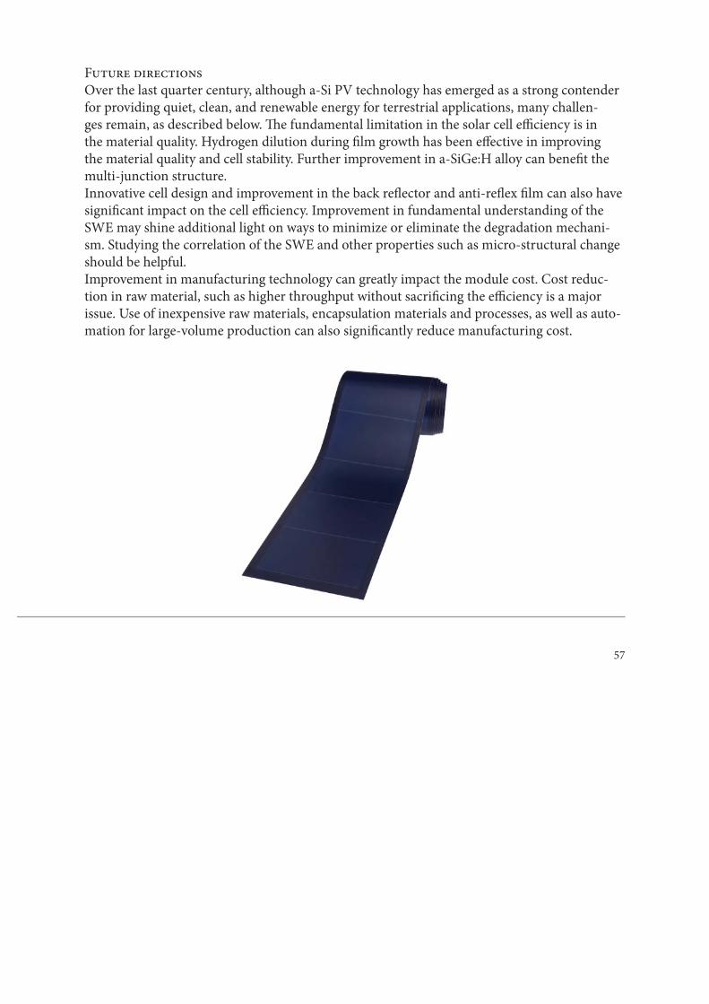
Future directionsOver the last quarter century, although a-Si PV technology has emerged as a strong contender for providing quiet, clean, and renewable energy for terrestrial applications, many challen-ges remain, as described below. Th e fundamental limitation in the solar cell effi ciency is in the material quality. Hydrogen dilution during fi lm growth has been eff ective in improving the material quality and cell stability. Further improvement in a-SiGe:H alloy can benefi t the multi-junction structure. Innovative cell design and improvement in the back refl ector and anti-refl ex fi lm can also have signifi cant impact on the cell effi ciency. Improvement in fundamental understanding of the SWE may shine additional light on ways to minimize or eliminate the degradation mechani-sm. Studying the correlation of the SWE and other properties such as micro-structural change should be helpful. Improvement in manufacturing technology can greatly impact the module cost. Cost reduc-tion in raw material, such as higher throughput without sacrifi cing the effi ciency is a major issue. Use of inexpensive raw materials, encapsulation materials and processes, as well as auto-mation for large-volume production can also signifi cantly reduce manufacturing cost.
58
Application of aSi PV
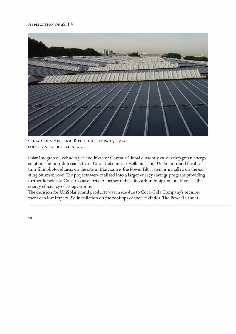
Coca-Cola Hellenic Bottling Company, Italysolution for bitumen roof
Solar Integrated Technologies and investor Contour Global currently co-develop green energy solutions on four diff erent sites of Coca-Cola bottler Hellenic using UniSolar brand fl exible thin-fi lm photovoltaics: on the site in Marcianise, the PowerTilt system is installed on the exi-sting bitumen roof. Th e projects were realized into a larger energy savings program providing further benefi ts to Coca-Cola’s eff orts to further reduce its carbon footprint and increase the energy effi ciency of its operations.Th e decision for UniSolar brand products was made due to Coca-Cola Company’s require-ment of a low impact PV-installation on the rooft ops of their facilities. Th e PowerTilt solu-
59
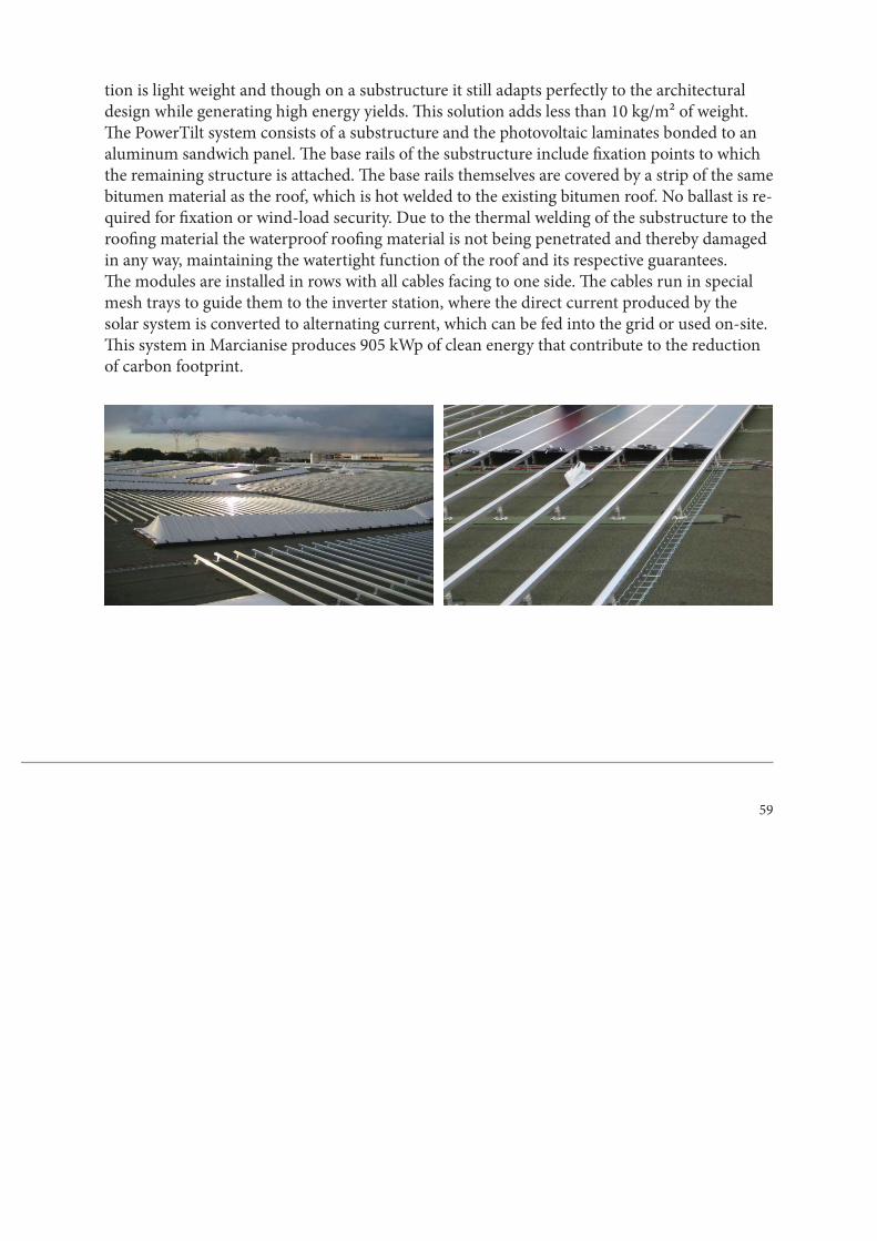
tion is light weight and though on a substructure it still adapts perfectly to the architectural design while generating high energy yields. Th is solution adds less than 10 kg/m² of weight. Th e PowerTilt system consists of a substructure and the photovoltaic laminates bonded to an aluminum sandwich panel. Th e base rails of the substructure include fi xation points to which the remaining structure is attached. Th e base rails themselves are covered by a strip of the same bitumen material as the roof, which is hot welded to the existing bitumen roof. No ballast is re-quired for fi xation or wind-load security. Due to the thermal welding of the substructure to the roofi ng material the waterproof roofi ng material is not being penetrated and thereby damaged in any way, maintaining the watertight function of the roof and its respective guarantees.Th e modules are installed in rows with all cables facing to one side. Th e cables run in special mesh trays to guide them to the inverter station, where the direct current produced by the solar system is converted to alternating current, which can be fed into the grid or used on-site.Th is system in Marcianise produces 905 kWp of clean energy that contribute to the reduction of carbon footprint.
60
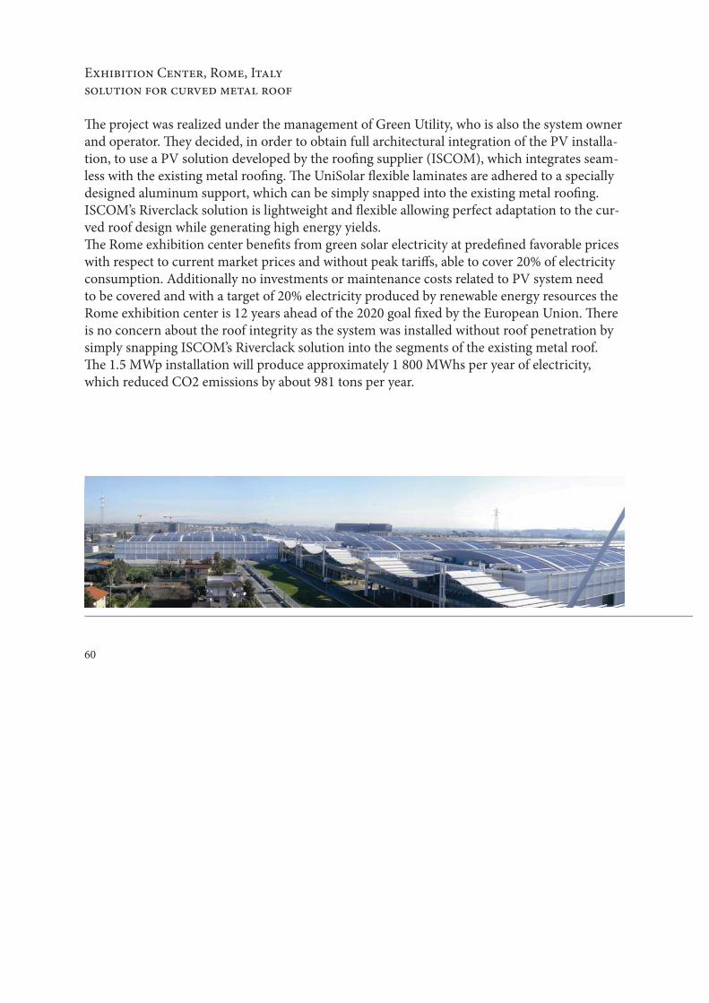
Exhibition Center, Rome, Italysolution for curved metal roof
Th e project was realized under the management of Green Utility, who is also the system owner and operator. Th ey decided, in order to obtain full architectural integration of the PV installa-tion, to use a PV solution developed by the roofi ng supplier (ISCOM), which integrates seam-less with the existing metal roofi ng. Th e UniSolar fl exible laminates are adhered to a specially designed aluminum support, which can be simply snapped into the existing metal roofi ng. ISCOM’s Riverclack solution is lightweight and fl exible allowing perfect adaptation to the cur-ved roof design while generating high energy yields.Th e Rome exhibition center benefi ts from green solar electricity at predefi ned favorable prices with respect to current market prices and without peak tariff s, able to cover 20% of electricity consumption. Additionally no investments or maintenance costs related to PV system need to be covered and with a target of 20% electricity produced by renewable energy resources the Rome exhibition center is 12 years ahead of the 2020 goal fi xed by the European Union. Th ere is no concern about the roof integrity as the system was installed without roof penetration by simply snapping ISCOM’s Riverclack solution into the segments of the existing metal roof.Th e 1.5 MWp installation will produce approximately 1 800 MWhs per year of electricity, which reduced CO2 emissions by about 981 tons per year.
61
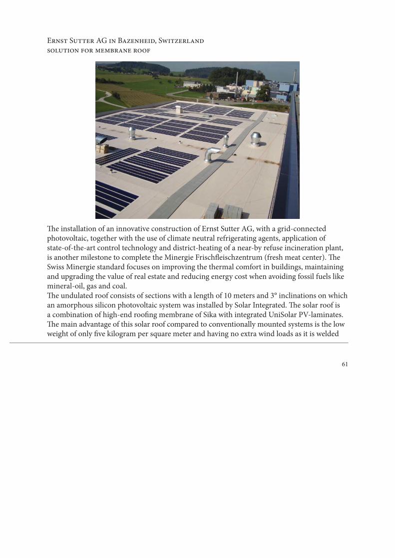
Ernst Sutter AG in Bazenheid, Switzerlandsolution for membrane roof
Th e installation of an innovative construction of Ernst Sutter AG, with a grid-connected photovoltaic, together with the use of climate neutral refrigerating agents, application of state-of-the-art control technology and district-heating of a near-by refuse incineration plant, is another milestone to complete the Minergie Frischfl eischzentrum (fresh meat center). Th e Swiss Minergie standard focuses on improving the thermal comfort in buildings, maintaining and upgrading the value of real estate and reducing energy cost when avoiding fossil fuels like mineral-oil, gas and coal.Th e undulated roof consists of sections with a length of 10 meters and 3° inclinations on which an amorphous silicon photovoltaic system was installed by Solar Integrated. Th e solar roof is a combination of high-end roofi ng membrane of Sika with integrated UniSolar PV-laminates. Th e main advantage of this solar roof compared to conventionally mounted systems is the low weight of only fi ve kilogram per square meter and having no extra wind loads as it is welded
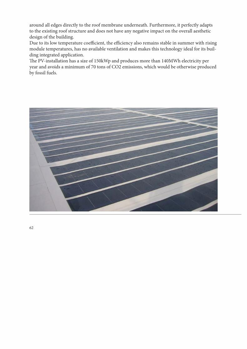
62
around all edges directly to the roof membrane underneath. Furthermore, it perfectly adapts to the existing roof structure and does not have any negative impact on the overall aesthetic design of the building.Due to its low temperature coeffi cient, the effi ciency also remains stable in summer with rising module temperatures, has no available ventilation and makes this technology ideal for its buil-ding integrated application. Th e PV-installation has a size of 150kWp and produces more than 140MWh electricity per year and avoids a minimum of 70 tons of CO2 emissions, which would be otherwise produced by fossil fuels.
63
CIGS Photovoltaic
CIGS is the acronym of copper-indium-gallium-(di)selenide, a chemical description of one of the most developed technologies in photovoltaic systems today. From 2000 this material deve-lop from an effi ciency of the 12-13% to a tested 19-20% by the NREL, the most important solar research center in the United States.Th e thin fl exible fi lms today on the market made with this technology raise an affi ciency of 14%, that made this thin fi lm the direct competitor for the crystalline modules. CIGS fi lms can be manufactured by several diff erent methods: the most common vacuum-ba-sed process co-evaporates or co-sputters copper, gallium, and indium,then anneals the resul-ting fi lm with a selenide vapor to form the fi nal CIGS structure. An alternative is to directly co-evaporate copper, gallium, indium and selenium onto a heated substrate. A non-vacuum-based alternative process deposits nanoparticles of the precursor materials on the substrate and then sinters them in situ. Electroplating is another low cost alternative to apply the CIGSlayer. Th e most important CIGS brands specifi cally designed thin fi lms for utility-scale systems, en-gineered to reduce total-system cost, the product is electrically and mechanically optimized for utility-scale solar power systems: this solution give competitivity to this product that for the fi rst time put on the market a PV product that cost less than 1$ by Watt.Th e driving forces for CIGS are compelling: potentially high effi ciency and low specifi c energyfor production. To these we may add the broad advantageous properties of thin-fi lm PV relati-ve to wafer-based PV: monolithic design leading to reduced parts handling, low consumption of both direct and indirect materials, and fewer process steps.Th e CIS is usually formed on a base electrode of molybdenum (Mo), chosen for its refracto-ry nature and good electrical conductivity. Th in-fi lm CIGS is a p-type semiconductor, and a junction is formed at the surface by deposition of a very thin layer of CdS. Th is creates an n-p homojunction just inside the CIGS, rather than a simple heterojunction. It is also possible to form eff ective junction without the use of CdS. Th e device is completed by deposition of a transparent conductor such as zinc oxide on top of the junction to help collect the light- ge-nerated current. Figure below shows typical C IGS solar module. In a manner similar to the defi nition and monolithic integration of thin-fi lm a-Si cells, individual CIGS cells are defi ned
64
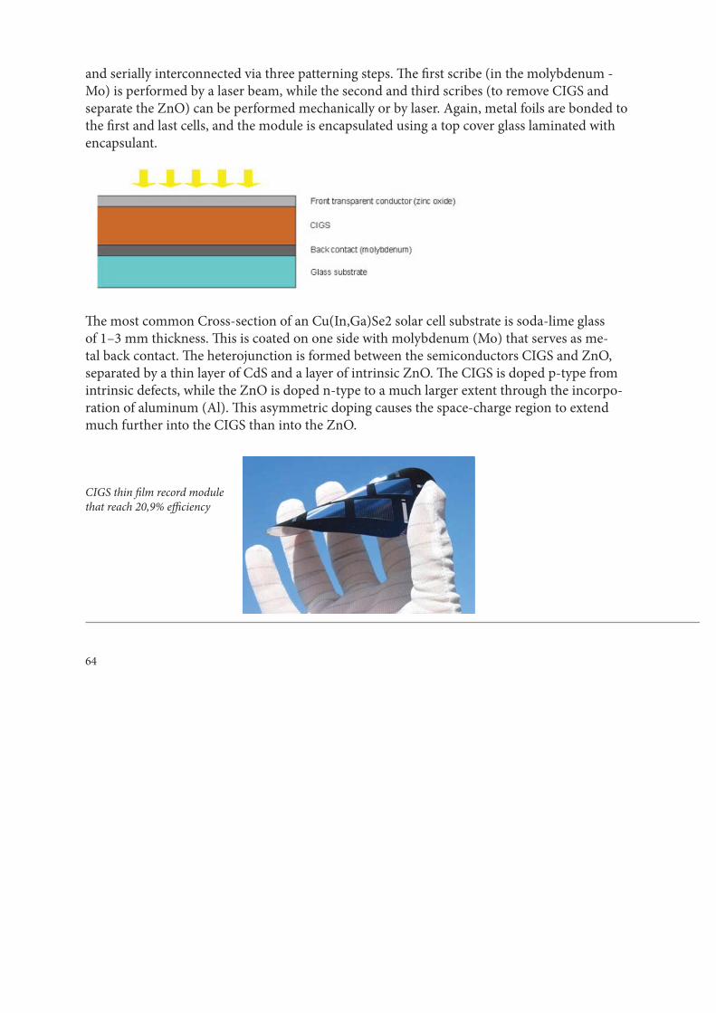
and serially interconnected via three patterning steps. Th e fi rst scribe (in the molybdenum - Mo) is performed by a laser beam, while the second and third scribes (to remove CIGS and separate the ZnO) can be performed mechanically or by laser. Again, metal foils are bonded to the fi rst and last cells, and the module is encapsulated using a top cover glass laminated with encapsulant.
Th e most common Cross-section of an Cu(In,Ga)Se2 solar cell substrate is soda-lime glass of 1–3 mm thickness. Th is is coated on one side with molybdenum (Mo) that serves as me-tal back contact. Th e heterojunction is formed between the semiconductors CIGS and ZnO, separated by a thin layer of CdS and a layer of intrinsic ZnO. Th e CIGS is doped p-type from intrinsic defects, while the ZnO is doped n-type to a much larger extent through the incorpo-ration of aluminum (Al). Th is asymmetric doping causes the space-charge region to extend much further into the CIGS than into the ZnO.
CIGS thin fi lm record module that reach 20,9% effi ciency
65
DevelopmentTh e demonstration of laboratory-scale, thin-fi lm CIGS solar cells reaching nearly 20%effi ciency helped to launch numerous start-up companies seeking to “grab the ring”—namely, to develop a low-cost, thin-fi lm product that performs as well as the best siliconbasedmodules. Th e entry point for many fi rms will be based on leaving a large gapbetween the champion device and the fi rst product effi ciencies; but these companies canenter commercial markets as long as their product can compete with the cost of other thinfi lmPV modules. Increasing CIGS module performance to values higher than competingthin-fi lm PV technologies could ultimately allow CIGS to achieve the lowest module costsand levelized cost of energy (LCOE) among all PV technologies. Hence, a primarychallenge is to provide the science and technology needed to close the gap in effi ciencybetween the entry-level prototype products and champion devices. A second challenge isto discover and qualify new materials and device schemes that can enhance performance,absorber bandgap and voltage, material usage, stability, yield, and process simplicity.Start-up companies have selected a multitude of processing approaches, which providesboth an opportunity as well as a challenge to improve commercial module effi ciency.Ultimately, we need to know at what point a chosen deposition or processing approachbecomes the dominant factor for limiting product performance. Building-integratedproducts may provide a signifi cant entry channel for CIGS thin-fi lm cells, takingadvantage of the demonstrated capability to manufacture fl exible cells (e.g., Global Solar,DayStar, Miasole, Ascent Solar, NanoSolar, ISET, and SoloPower) and the potential toconform the fi lm PV to building-material geometries. Th e absence of glass encapsulationsystems drives a second high-priority development to address the inherent devicesensitivity to water vapor. Developing a low-cost, fl exible, transparent package for CIGSthat will assure long (20-year-plus) outdoor module lifetime constitutes an enablingprerequisite for addressing this business segment.

66
Indium limitTh e ultimate impact of CIGS PV technology may be limited by the availability of indium. Estimates vary widely, but based on what is known today about In usage and In supply, a range of 2,000–10,000 MWp of annual module production may perhaps be established as a limit. To extend these limits, it would be highly desirable to use CIGS devices with much thinner absor-ber layers than used today (typically, 1.4–3 microns). Th is would also increase manufacturing throughput because thinner layers can be deposited in less time. Implementation will require the development of thin absorber cells without a loss in effi ciency, processing robustness, and module reliability. Alternatively, the family of chalcopyrite materials provides a rich set of options for engineering new absorber layers that could mimic the physical properties of CIGS needed to achieve similar remarkable effi ciencies—but also add important attributes such as avoiding indium, moving to a diff erent bandgap, increasing processing robustness, and provi-ding a clearer path to control of properties needed.
Nanosolar solutionNanosolar grows a thin fi lm semiconductor using a printing and annealing process that is far faster than conventional high vacuum deposition. Leverage recent advances in nanoscience to create high quality, highly uniform layers of nano-particles dispersed through their proprietary CIGS ink.Th is allows to utilize equipment from the industrial printing and roll-to-roll manufacturing industries to produce solar-electric foil at high speeds, bringing the economics of printing to the world of solar PV semiconductor manufacturing.Applying the latest in robotic manufacturing, primarily from the automotive industry, Na-nosolar assembles solar cells into solar panels with high throughput and high quality. Con-sistency in inspections, manufacturing and on-going testing is a critical part of Nanosolar’s production process.Th e key point is the realization of a small base module system that it’s easy to link and combine to obtain a full panel with high performances: on these modules the PV ink is deposited on a fl exible substrate (the “paper”), and then nanocomponents in the ink align themselves properly via molecular self-assembly.Nanosolar has developed a suite of in-house capabilities for creating nanostructured com-ponents based on various patented and patent-pending techniques. It uses nanostructured
67
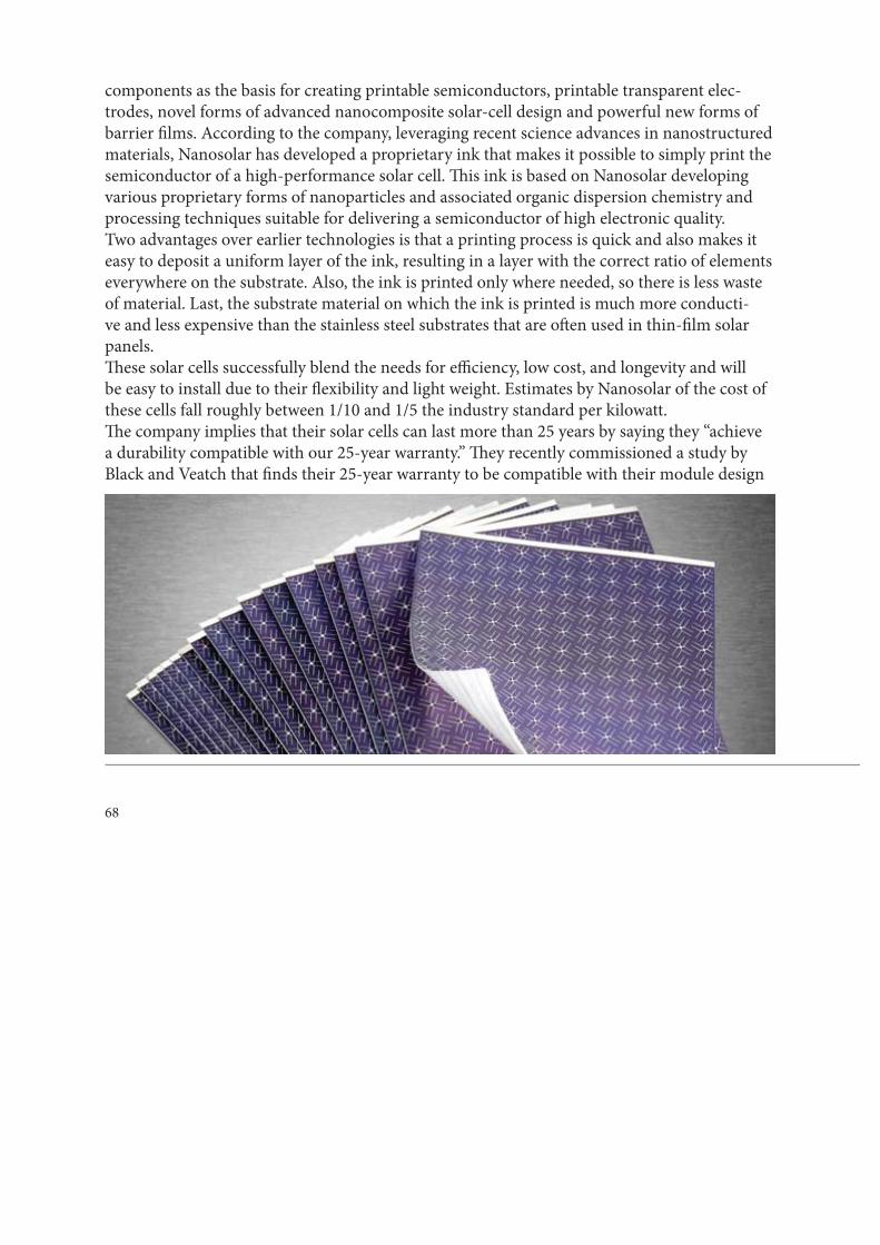
68
components as the basis for creating printable semiconductors, printable transparent elec-trodes, novel forms of advanced nanocomposite solar-cell design and powerful new forms of barrier fi lms. According to the company, leveraging recent science advances in nanostructured materials, Nanosolar has developed a proprietary ink that makes it possible to simply print the semiconductor of a high-performance solar cell. Th is ink is based on Nanosolar developing various proprietary forms of nanoparticles and associated organic dispersion chemistry and processing techniques suitable for delivering a semiconductor of high electronic quality.Two advantages over earlier technologies is that a printing process is quick and also makes it easy to deposit a uniform layer of the ink, resulting in a layer with the correct ratio of elements everywhere on the substrate. Also, the ink is printed only where needed, so there is less waste of material. Last, the substrate material on which the ink is printed is much more conducti-ve and less expensive than the stainless steel substrates that are oft en used in thin-fi lm solar panels.Th ese solar cells successfully blend the needs for effi ciency, low cost, and longevity and will be easy to install due to their fl exibility and light weight. Estimates by Nanosolar of the cost of these cells fall roughly between 1/10 and 1/5 the industry standard per kilowatt.Th e company implies that their solar cells can last more than 25 years by saying they “achieve a durability compatible with our 25-year warranty.” Th ey recently commissioned a study by Black and Veatch that fi nds their 25-year warranty to be compatible with their module design
69
CdTe Photovoltaic
Cadmium telluride PV is the fi rst thin fi lm photovoltaic technology that has surpassed crystal-line silicon PV in cheapness for a signifi cant portion of the PV market, namely in multi-kilo-watt systems. Since inception, the dominant solar cell technology in the marketplace has been based on wafers of crystalline silicon. During the same period, the idea of developing alternative, lower cost PV technologies led to the consideration of thin fi lms and concentrators. Th in fi lms are based on using thinner semiconductor layers to absorb and convert sunlight: concentrators, on the idea of replacing expensive semiconductors with lenses or mirrors. Both reduce cost, in theory, by reducing the use of semiconductor material. However, both faced critical challenges.Research in CdTe dates back to the 1950s: a simple heterojunction design evolved in which p-type CdTe was matched with n-type cadmium sulfi de (CdS). Th e cell was completed by adding top and bottom contacts. Early leaders in CdS/CdTe cell effi ciencies were GE in the 1960s and then Kodak, Monosolar, Matsushita, and AMETEK. By 1981, Kodak used close spaced subli-mation (CSS) and made the fi rst 10% cells and fi rst multi-cell devices (12 cells, 8% effi ciency, 30 cm2). Monosolar and AMETEK used electrodeposition, a popular early method. Matsushi-ta started with screen printing but shift ed in the 1990s to CSS. An important step forward occurred when cells were being scaled-up in size to make larger area products called modules. Th ese products require higher currents than small cells and it was found that an additional layer, called a transparent conductive oxide (TCO), could facilitate the movement of current across the top of the cell (instead of a metal grid). Made more conductive for PV, tin oxide became and remains the norm in CdTe PV modules.Professor Ting L. Chu of Southern Methodist University, made signifi cant contributions to moving the effi ciency of CdTe cells to above 15% in 1992, a critical level of success in terms of potential commercial competitiveness. Th is was done when he added an intervening or buff er layer to the TCO/CdS/CdTe stack and then thinned the CdS to allow more light through. Chu used resistive tin oxide as the buff er layer and then thinned the CdS from several micrometres to under half a micrometre in thickness. Th ick CdS, as it was used in prior devices, blocked about 5 mA/cm2 of light, or about 20% of the light usable by a CdTe device. By removing this loss while maintaining the other properties of the device, Chu reached 15% effi ciency in 1991,
70
the fi rst thin fi lm to do so, as verifi ed at the National Renewable Energy Laboratory(NREL). Chu used CSS for depositing the CdTe. For his achievements in taking CdTe from its status as “also-ran” to a primary candidate for commercialization, some think of Ting L. Chu as the key technologist in the history of CdTe development. Th e major commercial success to emerge from the turmoil of the 1990s was Solar Cells In-corporated (SCI). Founded in 1990 as an outgrowth of a prior company, Glasstech Solar, led by inventor-entrepreneur Harold McMaster, it switched from amorphous silicon to CdTe as a better solution to the higher-cost crystalline silicon PV. McMaster championed CdTe for its high-rate, high-throughput processing. In February 1999, he sold the company to True North Partners, an investment arm of the Walton family, owners of Wal-Mart: John T. Walton joined the Board of the new company, and Mike Ahearn of True North became the CEO of the newly minted First Solar.In its early years First Solar suff ered setbacks, and initial module effi ciencies were modest, about 7%. Commercial product became available in 2002. But production did not reach 25 megawatts until 2005. Th e company built an additional line in Perrysburg, Ohio, then four lines in Germany, supported by the substantial production incentives (about 50% of capital costs). In 2006 First Solar reached 75 MW of annual production and announced a further 16 lines in Malaysia. As of 2008, First Solar is producing at nearly half a gigawatt annual rate, and in 2006 and 2007 was among the largest PV module manufacturers in the world. Cell effi ciencyBest cell effi ciency has plateaued at 16.5% since 2001. Th e opportunity to increase current has been almost fully exploited, but more diffi cult challenges associated with junction quality, with properties of CdTe and with contacting have not been as successful. However, the number of active scientists in CdTe PV was small: improved doping of CdTe and increased understanding of key processing steps are keys to progress. Since CdTe has the optimal band gap for single-junction devices, it may be expected that effi ciencies close to exceeding 20% (such as already shown in CIS alloys) should be achievable in practical CdTe cells. Modules of 15%would then be possible. Perhaps the most subtle and least understood problem with CdTe PV is the supply of tellurium (Te): it is an element not currently used for many applications. Only a small amount, estimated to be about 800 metric tons per year, is available. According to USGS, global tellurium pro-
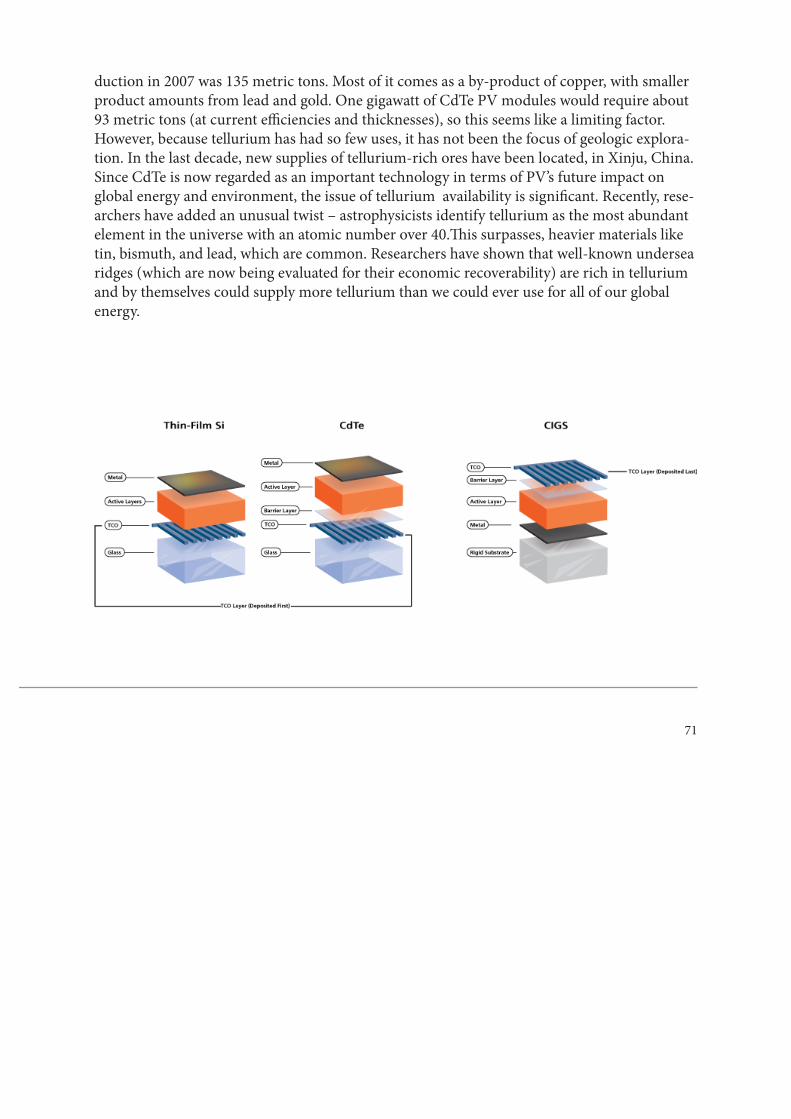
71
duction in 2007 was 135 metric tons. Most of it comes as a by-product of copper, with smaller product amounts from lead and gold. One gigawatt of CdTe PV modules would require about 93 metric tons (at current effi ciencies and thicknesses), so this seems like a limiting factor. However, because tellurium has had so few uses, it has not been the focus of geologic explora-tion. In the last decade, new supplies of tellurium-rich ores have been located, in Xinju, China. Since CdTe is now regarded as an important technology in terms of PV’s future impact on global energy and environment, the issue of tellurium availability is signifi cant. Recently, rese-archers have added an unusual twist – astrophysicists identify tellurium as the most abundant element in the universe with an atomic number over 40.Th is surpasses, heavier materials like tin, bismuth, and lead, which are common. Researchers have shown that well-known undersea ridges (which are now being evaluated for their economic recoverability) are rich in tellurium and by themselves could supply more tellurium than we could ever use for all of our global energy.
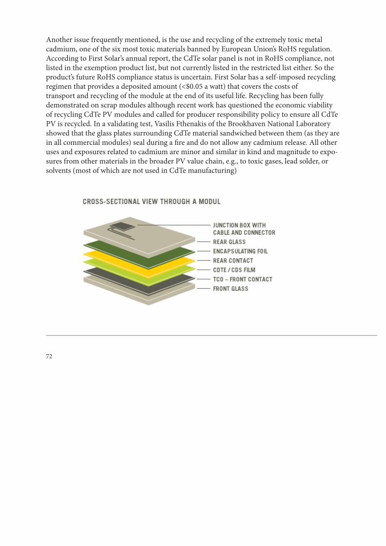
72
Another issue frequently mentioned, is the use and recycling of the extremely toxic metal cadmium, one of the six most toxic materials banned by European Union’s RoHS regulation. According to First Solar’s annual report, the CdTe solar panel is not in RoHS compliance, not listed in the exemption product list, but not currently listed in the restricted list either. So the product’s future RoHS compliance status is uncertain. First Solar has a self-imposed recycling regimen that provides a deposited amount (<$0.05 a watt) that covers the costs oftransport and recycling of the module at the end of its useful life. Recycling has been fully demonstrated on scrap modules although recent work has questioned the economic viability of recycling CdTe PV modules and called for producer responsibility policy to ensure all CdTe PV is recycled. In a validating test, Vasilis Fthenakis of the Brookhaven National Laboratory showed that the glass plates surrounding CdTe material sandwiched between them (as they are in all commercial modules) seal during a fi re and do not allow any cadmium release. All other uses and exposures related to cadmium are minor and similar in kind and magnitude to expo-sures from other materials in the broader PV value chain, e.g., to toxic gases, lead solder, orsolvents (most of which are not used in CdTe manufacturing)
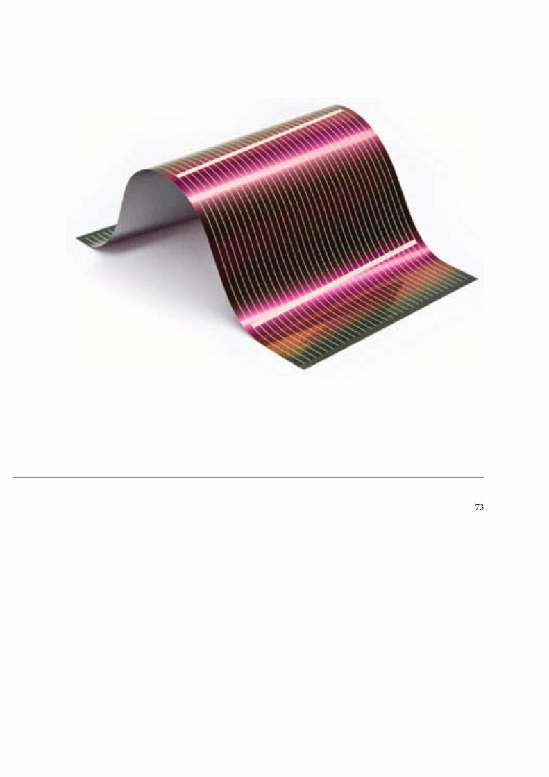
73
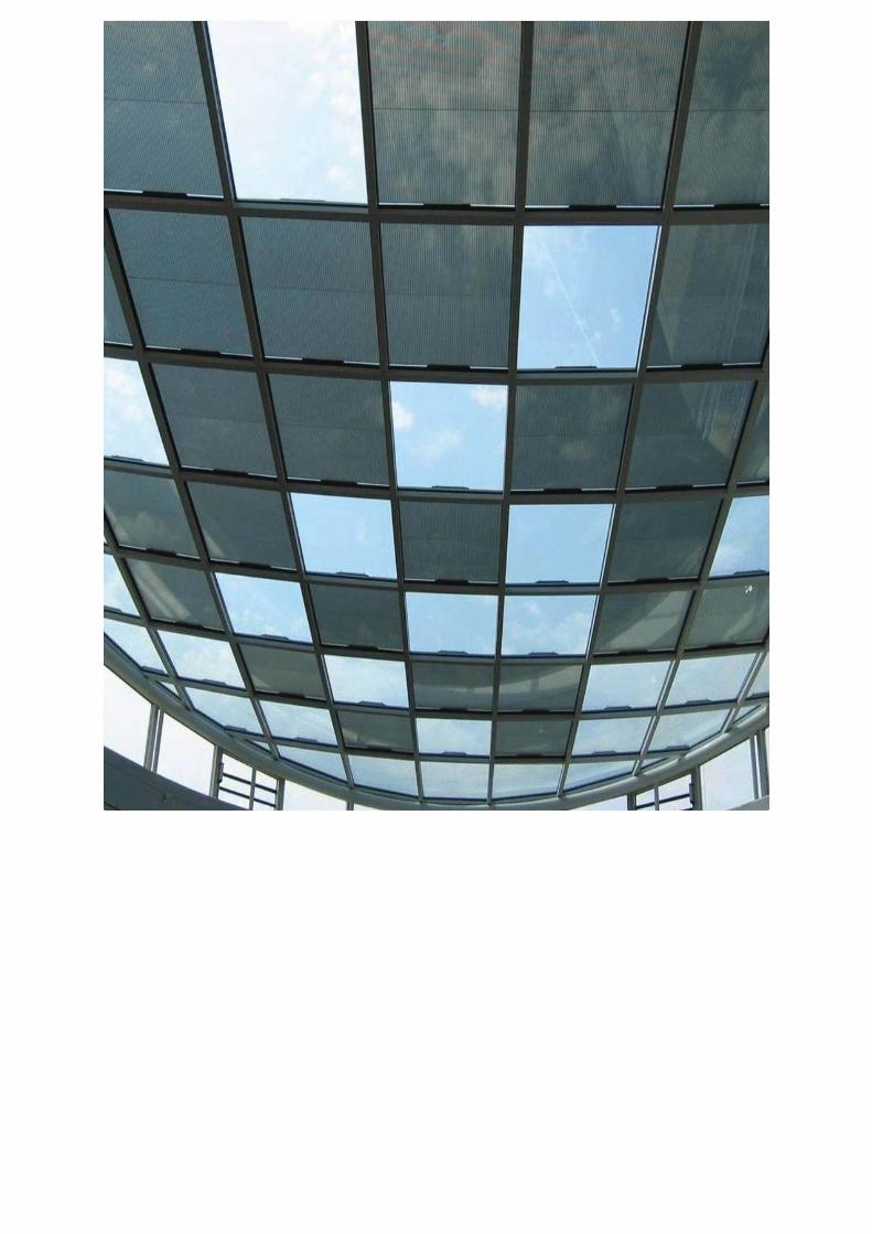

TRANSPARENT
PHOTOVOLTAIC
FILMS
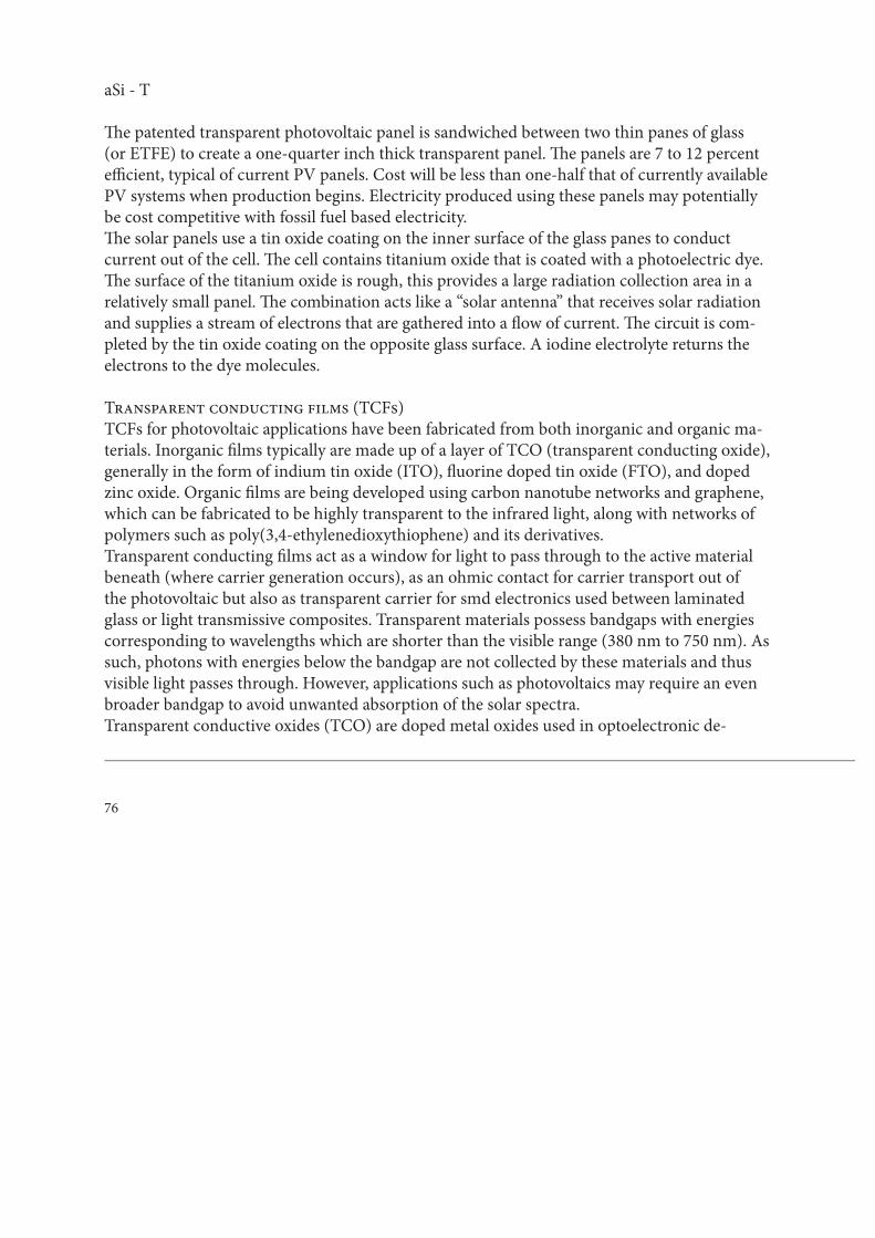
76
aSi - T
Th e patented transparent photovoltaic panel is sandwiched between two thin panes of glass (or ETFE) to create a one-quarter inch thick transparent panel. Th e panels are 7 to 12 percent effi cient, typical of current PV panels. Cost will be less than one-half that of currently available PV systems when production begins. Electricity produced using these panels may potentially be cost competitive with fossil fuel based electricity. Th e solar panels use a tin oxide coating on the inner surface of the glass panes to conduct current out of the cell. Th e cell contains titanium oxide that is coated with a photoelectric dye. Th e surface of the titanium oxide is rough, this provides a large radiation collection area in a relatively small panel. Th e combination acts like a “solar antenna” that receives solar radiation and supplies a stream of electrons that are gathered into a fl ow of current. Th e circuit is com-pleted by the tin oxide coating on the opposite glass surface. A iodine electrolyte returns the electrons to the dye molecules.
Transparent conducting films (TCFs) TCFs for photovoltaic applications have been fabricated from both inorganic and organic ma-terials. Inorganic fi lms typically are made up of a layer of TCO (transparent conducting oxide), generally in the form of indium tin oxide (ITO), fl uorine doped tin oxide (FTO), and doped zinc oxide. Organic fi lms are being developed using carbon nanotube networks and graphene, which can be fabricated to be highly transparent to the infrared light, along with networks of polymers such as poly(3,4-ethylenedioxythiophene) and its derivatives.Transparent conducting fi lms act as a window for light to pass through to the active material beneath (where carrier generation occurs), as an ohmic contact for carrier transport out of the photovoltaic but also as transparent carrier for smd electronics used between laminated glass or light transmissive composites. Transparent materials possess bandgaps with energies corresponding to wavelengths which are shorter than the visible range (380 nm to 750 nm). As such, photons with energies below the bandgap are not collected by these materials and thus visible light passes through. However, applications such as photovoltaics may require an even broader bandgap to avoid unwanted absorption of the solar spectra.Transparent conductive oxides (TCO) are doped metal oxides used in optoelectronic de-
77
vices such as fl at panel displays and photovoltaics. Most of these fi lms are fabricated with polycrystalline or amorphous microstructures. On average, these applications use electrode materials that have greater than 80% transmittance of incident light as well as conductivities higher than 103 S/cm for effi cient carrier transport. Th e transmittance of these fi lms, just as in any transparent material, is limited by light scattering at defects and grain boundaries. In gene-ral, TCOs for use as thin-fi lm electrodes in solar cells should have a minimum carrier concen-tration on the order of 1020 cm3 for low resistivity and a bandgap greater than 380 nm to avoid absorption of light over most of the solar spectra. Mobility in these fi lms is limited by ionized impurity scattering and is on the order of 40 cm2/(V·s). Current transparent conducting oxides used in industry are primarily n-type conductors, meaning their primary conduction is from the fl ow of electrons. Suitable p-type transparent conducting oxides are still being researched.To date, the industry standard in TCO is ITO, or tin-doped indium-oxide. Th is material boasts a low resistivity of ~10−4 Ω·cm and a transmittance of greater than 80%. However ITO has the drawback of being expensive. Indium, the fi lm’s primary metal, is rare, and its price fl uctuates due to market demand: for this reason, doped binary compounds such as aluminum-doped zinc-oxide (AZO) and indium-doped cadmium-oxide have been proposed as alternative mate-rials. AZO is composed of aluminum and zinc, two common and inexpensive materials, while indium-doped cadmium oxide only uses indium in low concentrations.
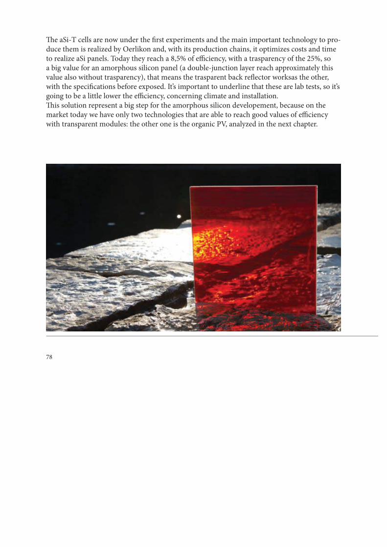
78
Th e aSi-T cells are now under the fi rst experiments and the main important technology to pro-duce them is realized by Oerlikon and, with its production chains, it optimizes costs and time to realize aSi panels. Today they reach a 8,5% of effi ciency, with a trasparency of the 25%, so a big value for an amorphous silicon panel (a double-junction layer reach approximately this value also without trasparency), that means the trasparent back refl ector worksas the other, with the specifi cations before exposed. It’s important to underline that these are lab tests, so it’s going to be a little lower the effi ciency, concerning climate and installation.Th is solution represent a big step for the amorphous silicon developement, because on the market today we have only two technologies that are able to reach good values of effi ciency with transparent modules: the other one is the organic PV, analyzed in the next chapter.
79
Is Organic PV the Future of Solar?By Stephen Lacey
Massachusetts, United States - When Dr. Alan Heeger and his colleagues began experimenting with newlyfoundsemiconducting polymers in the 1970s, they just wanted to understand the basic physics of how electrons were set free in the materials. But they ended up making a discovery that has helped advance a new generation of solar plastics and inks. By oxidizing polyacetylene, a long-chain molecule which acts like a pigment, the researchers found the polymer to have extraordinarily high conductive properties. “We realized it in a classic ‘ah ha moment,’” says Heeger. “But then over and over again, we saw additionalproperties that we had not foreseen.” Eventually, Heeger and his colleagues, Alan MacDiarmind and Hideki Shirakawa, fi gured out that the materialwas not just a novelty. It had the potential to change the way we manufacture electronic devices, transistors,diodes and solar cells. Th ese semiconducting polymers could be put in a solution and printed on a substrate –potentially creating a revolution in electronics that rivals what Gutenberg’s printing press did for books 600years earlier.“Printing is a low-cost, high speed manufacturing process...I doubt that there’s a lower-cost manufacturing forany solar technology,” says Heeger.Th e science community agreed. In 2000, the three researchers received the Nobel Prize in chemistry for theirwork. A year later Heeger co-founded Konarka, a Massachussets-based company working to commercialize orga-nic solar PV technologies. Th e company has since racked up tens of millions of dollars in fi nancing and has built a GW-scale manufacturing facility that produces “power plastic,” a fl exible material that can be integrated into bags, electronics, and building materials. With all this promising sounding news, one might think that the revolution in printed organic PV is underway. But that’s defi nitely not the case. A number of technical challenges and changing market conditions have made it diffi cult for third-generation solar companies to ramp up production and sell products.“Clearly the industry had a good story to tell,” says technology journalist Peter Fairley. “But that story has since changed and I think things look very diff erent today for these companies.”During the height of the silicon shortage between 2005 and 2007, interest in emerging third-generation solar technologies was strong. Th e high price of silicon made printable, non-silicon based solar products look very attractive. Never mind that they were only 4 to 5 percent effi cient and lasted for only a few years: roll-to-roll prin-ting below a dollar per watt was an attractive selling point.Th en came Cadmium Telluride thin-fi lm producer First Solar, which said it was manufacturing 11% effi cient products below a dollar per watt. It quickly steamrolled its way to the top of global module producers.Th e eventual easing of the silicon shortage and the global oversupply of PV caused a roughly 30% drop inprices, making traditional PV technologies more attractive than they’ve ever been. Th is has taken some of thespotlight off the third-gen PV industry as well. Konarka may have a GW-scale manufacturing facility, but they don’t appear to be shipping anywhere close to that amount of product.
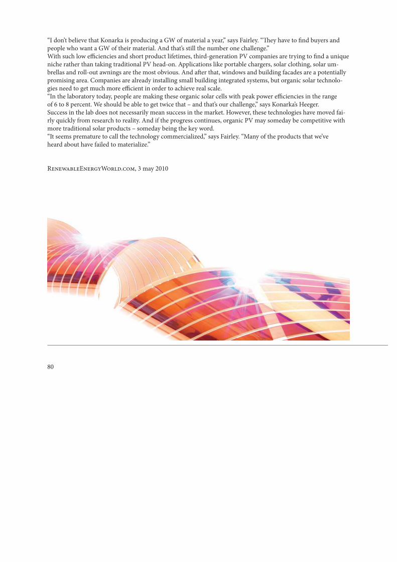
80
“I don’t believe that Konarka is producing a GW of material a year,” says Fairley. “Th ey have to fi nd buyers andpeople who want a GW of their material. And that’s still the number one challenge.”With such low effi ciencies and short product lifetimes, third-generation PV companies are trying to fi nd a unique niche rather than taking traditional PV head-on. Applications like portable chargers, solar clothing, solar um-brellas and roll-out awnings are the most obvious. And aft er that, windows and building facades are a potentially promising area. Companies are already installing small building integrated systems, but organic solar technolo-gies need to get much more effi cient in order to achieve real scale. “In the laboratory today, people are making these organic solar cells with peak power effi ciencies in the rangeof 6 to 8 percent. We should be able to get twice that – and that’s our challenge,” says Konarka’s Heeger.Success in the lab does not necessarily mean success in the market. However, these technologies have moved fai-rly quickly from research to reality. And if the progress continues, organic PV may someday be competitive with more traditional solar products – someday being the key word. “It seems premature to call the technology commercialized,” says Fairley. “Many of the products that we’veheard about have failed to materialize.”
RenewableEnergyWorld.com, 3 may 2010
81
Organic Photovoltaic
Solution processable organic photovoltaics (OPV) are currently being intensively investigated because this technology represents the best chance for developing a PV product in Zone II. Th e major advantages of using conjugated organic materials for PV units rather than inorga-nics are the low material and substrate costs and the ease of printing and fabrication. However,OPV devices are currently far less effi cient and have shorter lifetimes than inorganic solar cells. Th e combination of low material and fabrication costs for OPV promises to reduce the unit cost by 10. Th is cost savings is based on the idea that mass production will decrease material costs and that fabrication can be performed in a reel-to-reel format onto fl exible substrates. Th e resulting economic balance will yield a reduction in the costper-Watt for power produced from OPV devices when the device power conversion effi ciency nears 10%.
EvolutionTh e fi rst OPV device was fabricated by Tang at Kodak and had a power conversion effi ciency of 1,1%. Th is fi rst device was a bilayer stack of copper phthalocyanine as the electron donor and a perylene tetracarboxylic derivative for the electron acceptor with a standard p-n connec-tion. Th is initial design was only able to deliver a low conversion effi ciency because the light-induced excited states (excitons) are tightly bound in organic molecules and can only separate at donor/acceptor interfaces. Typical exciton diff usion lengths are 5–25 nm: this small exciton diff usion length places a fundamental limit on the thickness that a material layer can have since light absorbed further from the interface will not result in charge separation and photo-current. In the early 90s a new design for OPV active layers was developed called the bulk-heterojun-ction (BHJ). Th is layers consist of a mixture of donor and acceptor species in a mixture of a common solvent: as the solvent rapidly evaporates, phase separation occurs between the two components. Th e degree of phase separation is determined by the solubility of the components in the solvent, the peed with which the fi lm dries, and the mutual solubility of components in each other.Th e new BHJ design has the major advantage that the distancebetween the donor and acceptor in the layer is reduced and theprobability of charge separation approaches unity. However, the
82
mixed fi lm has reduced order, leading to a less charge mobility, greater trap density and island domains that do not have a charge transport pathway to either electrode. Until 2007, nearly all increases in OPV device of power effi ciency came about as a result improved BHJ layer morphology. For example, Shaheen found that using a solvent with improved mutual solubility for the two components could reduce the domain size: switching from the solvent toluene to chlorobenzene improved the effi ciency from 0.9% to 2.5%. Next it was discovered that the application of thermal treatment could be used to improve the hole mobility, increase crystallinity and increase effi ciency. Simultaneously, it was found that the use of high-boiling-point solvents and long solvent- soaking times could optimize the morphology through self assembly. Finally, it was found that the morphology could be optimi-zed by using low-concentration additives, that could improve morphology either by selectively dissolving one of the components or by causing rapid crystallization of the polymer during drying. All of the thermal, solvent, and additive techniques increase the effi ciency from 1% to >4%. An important research theme for the last 15 years has been the determination of the mechanism for photocurrent production in a bulk heterojunction: photons with energy abo-ve the optical band gap (Eg) are absorbed in the active layer by both the donor and acceptor materials, but since the donor polymer has a much larger absorption coeffi cient, the polymer typically absorbs the majority of the light. In a BHJ, the exciton has a high probability of diff u-sing to a donor–acceptor interface and separating into a geminate charge pair. Th is geminate or bound pair, also known as a charge-transfer exciton, consists of a Coulombically bound hole on the donor and electron on the acceptor. Th e bound charge pair can be separated into free charges at room temperature when a suffi cient electric fi eld is applied. Th is built-in electric fi eld is generated by sandwiching the BHJ layer between electrodes that have diff ering work functions. Finally, the free charges can hop from site-to-site under the infl uence of the built-in fi eld until they reach their respective electrodes. Bound charge pairs can reform from free charges. Both bound pairs and free charges can recombine.Since 2007, a number of new record effi ciencies have been reported that can be directly attri-buted to improved synthetic design of either the donor or acceptor. Th ree successful synthetic strategies can be identifi ed. First, the short circuit current density can be increased by lowering the Eg and maintaining the polymer HOMO–fullerene LUMO spacing. Th e second possibility is to increase the open circuit voltage Voc by maintaining the
83
Eg but shift ing the both the HOMO (highest occupied molecular orbital) and LUMO (singu-larly unoccupied molecular orbital) of the polymer down in energy. Th e third possibility is to increase the Voc while maintaining the Eg by raising the LUMO level of the fullerene. Two scientists have predicted that these combined adjustments can yield power effi ciencies of over 10%. A series of new co-polymer donors synthetized reach record effi ciencies of 5,4%, 6,4%, and 7,9%. All of the published results used various new push–pull polymers to achieve the high effi ciencies. Th e domain size, crystallinity, and curing method (temperature, solvent soak, or solvent ad-ditive) can now be chosen for these mixtures. A better understanding of optical and electrical loss mechanisms has also been gained for these mixtures. But, there is still quite a lot of aca-demic research that needs to be performed in all three of these areas. Hopefully, the scientifi c community will have increased access to the new low-band-gap co-polymers for morphology and device physics studies in the near future.
ProductionFabrication of an OPV device involves four broad sequential steps. First, a conducting sub-strate with an optimized work function and surface energy is created. Second, a BHJ layer is coated onto the substrate. Next a second electrode is deposited onto the BHJ layer. Finally, the device is encapsulated in a material that protects the active layers from exposure to H2O, O2, and UV irradiation. To optimize costs of production, in order to be competitive with the other solar producers, it’s used a roll-to-roll fabrication: in this sense, OPV devices can either be regular (holes move towards the substrate) or inverted (holes move away from the substrate). Th e direction of current fl ow is determined by the choice of electrode materials. One of the requirements for reel-to-reel coating is that the substrate has to be fl exible so that it can be pul-led through the reels. Regular devices can be fabricated onto transparent plastic foils that have been coated with a transparent conducting oxide (TCO) such as ITO, ZnO:Al or SnO2:F.Preparation of the substrate electrode requires similar steps for both device types. First the electrode must be either etched into the required shape or a resistive coating must be applied to prevent shorts where the electrodes will be externally contacted. Th en the substrate material must be extensively cleaned and the electrode materials coated with a layer of material that sets the work function.
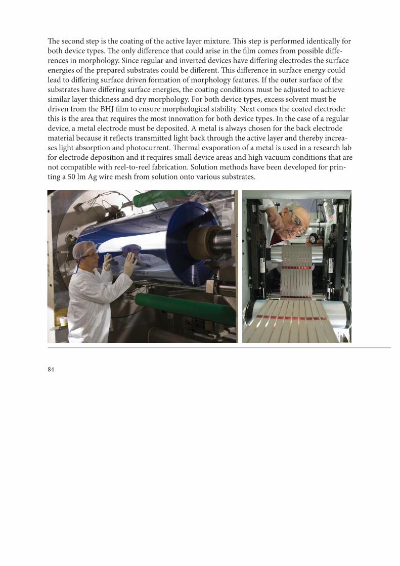
84
Th e second step is the coating of the active layer mixture. Th is step is performed identically for both device types. Th e only diff erence that could arise in the fi lm comes from possible diff e-rences in morphology. Since regular and inverted devices have diff ering electrodes the surface energies of the prepared substrates could be diff erent. Th is diff erence in surface energy could lead to diff ering surface driven formation of morphology features. If the outer surface of the substrates have diff ering surface energies, the coating conditions must be adjusted to achieve similar layer thickness and dry morphology. For both device types, excess solvent must be driven from the BHJ fi lm to ensure morphological stability. Next comes the coated electrode: this is the area that requires the most innovation for both device types. In the case of a regular device, a metal electrode must be deposited. A metal is always chosen for the back electrode material because it refl ects transmitted light back through the active layer and thereby increa-ses light absorption and photocurrent. Th ermal evaporation of a metal is used in a research lab for electrode deposition and it requires small device areas and high vacuum conditions that are not compatible with reel-to-reel fabrication. Solution methods have been developed for prin-ting a 50 lm Ag wire mesh from solution onto various substrates.
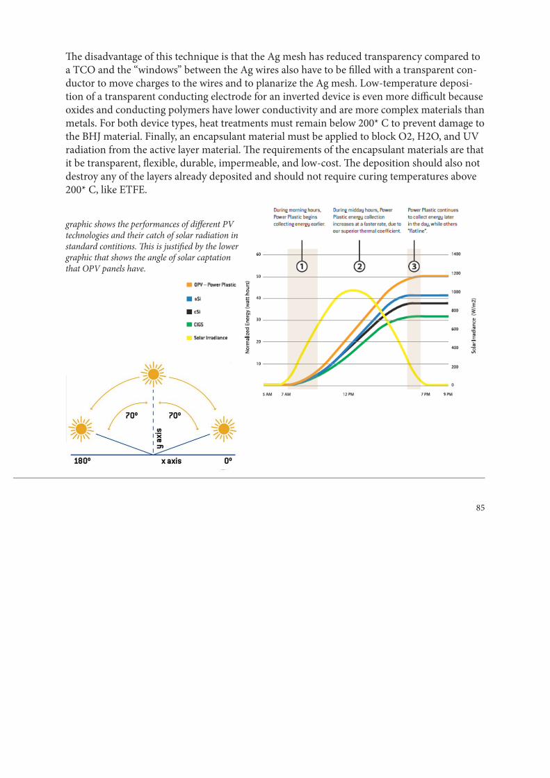
85
Th e disadvantage of this technique is that the Ag mesh has reduced transparency compared to a TCO and the ‘‘windows” between the Ag wires also have to be fi lled with a transparent con-ductor to move charges to the wires and to planarize the Ag mesh. Low-temperature deposi-tion of a transparent conducting electrode for an inverted device is even more diffi cult because oxides and conducting polymers have lower conductivity and are more complex materials than metals. For both device types, heat treatments must remain below 200* C to prevent damage to the BHJ material. Finally, an encapsulant material must be applied to block O2, H2O, and UV radiation from the active layer material. Th e requirements of the encapsulant materials are that it be transparent, fl exible, durable, impermeable, and low-cost. Th e deposition should also not destroy any of the layers already deposited and should not require curing temperatures above 200* C, like ETFE.
graphic shows the performances of diff erent PV technologies and their catch of solar radiation in standard contitions. Th is is justifi ed by the lower graphic that shows the angle of solar captation that OPV panels have.
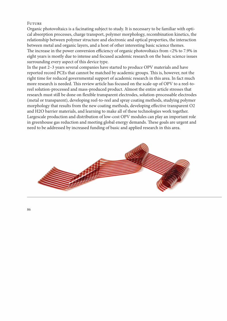
86
FutureOrganic photovoltaics is a facinating subject to study. It is necessary to be familiar with opti-cal absorption processes, charge transport, polymer morphology, recombination kinetics, the relationship between polymer structure and electronic and optical properties, the interaction between metal and organic layers, and a host of other interesting basic science themes. Th e increase in the power conversion effi ciency of organic photovoltaics from <2% to 7.9% in eight years is mostly due to intense and focused academic research on the basic science issues surrounding every aspect of this device type.In the past 2–3 years several companies have started to produce OPV materials and have reported record PCEs that cannot be matched by academic groups. Th is is, however, not the right time for reduced governmental support of academic research in this area. In fact much more research is needed. Th is review article has focused on the scale-up of OPV to a reel-to-reel solution-processed and mass-produced product. Almost the entire article stresses that research must still be done on fl exible transparent electrodes, solution-processable electrodes (metal or transparent), developing reel-to-reel and spray coating methods, studying polymermorphology that results from the new coating methods, developing eff ective transparent O2 and H2O barrier materials, and learning to make all of these technologies work together. Largescale production and distribution of low-cost OPV modules can play an important role in greenhouse gas reduction and meeting global energy demands. Th ese goals are urgent and need to be addressed by increased funding of basic and applied research in this area.
87
San Francisco MTA Transit ShelterKonarka Technologies, Lundberg Design, 3form, Clear Channel Outdoor
In 2008 San Francisco Municipal Transportation Agency (MTA) decided to upgrade the city’s urban transit shelters: it wanted to bring new technology and innovative thinking to the chal-lenge. Its goals were both functional and aesthetic, so the shelter had to provide comfortable seats for bus passengers, look great on the street, and refl ect the city’s unique qualities, while the solution has to be durable enough to survive harsh urban conditions for as long as 25 years.As part of the city’s extensive commitment to green technology, the new design also had to in-tegrate the latest advances in environmental effi ciency and sustainability: from solar power to recycled materials. Designers submitted dozens of diff erent approaches, which were ultimately displayed at City Hall as models. Aft er the inherently long process was over, a creative approach spearheaded by Lundberg De-sign (and its client, Clear Channel Outdoor) won thecontest, and the contract.A critical diff erentiating element of the design is its unique, red/amber undulating roof, which references the legendary hills of the city, the waves of the San Francisco Bay, and seismic wa-ves. Embedded within this translucent roof, you’ll fi nd Konarka Power Plastic®, which enables the transit shelters to generate power and be largely self-suffi cient from an energy perspective. Power generated by Power Plastic is used to fuel LED lighting at night, “NextBus” LED signa-ge, and built-in Wi-Fi routers that provide free access to commuters.In fact, Konarka Power Plastic panels not only power the structure, but also create new solar power for the city via two-way connections to the power grid. Ultimately, the city expects that the new transit shelters will channel an estimated 43,000 kilowatt-hours back into the grid annually. Th e new design transforms transit shelters from power consumers into power gene-rators, all while providing the protection and information that travelers rely on. Plus it intro-duces new capabilities, such as Internet access, that enhance the overall experience: capabilities fueled by Power Plastic.Starting with a prototype shelter on a residential section of Geary Street, new shelters are rolling out throughout the city. Of the more than 1,200 shelters of various sizes, about 300 will include solar capability fueled by Konarka Power Plastic. Some shelters are located in low light areas where any solar capability would be impractical.
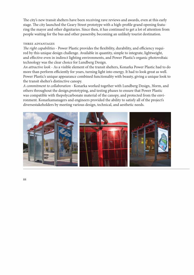
88
Th e city’s new transit shelters have been receiving rave reviews and awards, even at this early stage. Th e city launched the Geary Street prototype with a high-profi le grand opening featu-ring the mayor and other dignitaries. Since then, it has continued to get a lot of attention from people waiting for the bus and other passersby, becoming an unlikely tourist destination.
three advantagesTh e right capabilities - Power Plastic provides the fl exibility, durability, and effi ciency requi-red by this unique design challenge. Available in quantity, simple to integrate, lightweight, and eff ective even in indirect lighting environments, and Power Plastic’s organic photovoltaic technology was the clear choice for Lundberg Design.An attractive look - As a visible element of the transit shelters, Konarka Power Plastic had to do more than perform effi ciently for years, turning light into energy. It had to look great as well. Power Plastic’s unique appearance combined functionality with beauty, giving a unique look to the transit shelter’s distinctive canopy.A commitment to collaboration - Konarka worked together with Lundberg Design, 3form, and others throughout the design,prototyping, and testing phases to ensure that Power Plastic was compatible with thepolycarbonate material of the canopy, and protected from the envi-ronment. Konarkamanagers and engineers provided the ability to satisfy all of the project’s diversestakeholders by meeting various design, technical, and aesthetic needs.
89
Spherical Solar Cell
Th e Japanese company Kyosemi Corporation has developed a spherical solar cell called the Sphelar. Given the spherical like shape, Sphelar is capable of greater power effi ciency and fl exi-bility in applications than conventional fl at solar cell panels. Th e product measures 1 mm in diameter and it’s a crystallization of a little silicon sphere obtai-ned in a particular extrusion process.Conventional fl at solar cells were unable to eff ectively harness this indirect light. In addition, the sun takes on a many diff erent positions according to the season and time of day, so in order to obtain a stable supply of power, there was a need to change the orientation of the solar cell by constantly following the sun. Sphelar captures light from all directions, which means it can catch refl ected light and diff used light. In addition, there is no need for the superfl uous operation of tracking the sun. Th e spherical light-receiving surfaces achieve unprecedented high generation effi ciency. Th e Sphelar light sensitive surface is therefore able to achieve high energy effi ciency. When assembled in a panel fashion, resulting modules are said to have a conversion effi ciency of almost 20%.Th e unique design of the Sphelar with a diameter of only 1 mm to 1.5 mm allows it to be installed in a variety of energy effi cient settings. It can be placed in a parallel format or in a se-ries. Th e advantage of the Sphelar is that it will not block views as some conventional fl at solar cell panels have been found to do.Sphelar is effi cient from a manufacturing stand point. As opposed to conventional fl at solar cell manufacturing the Sphelar has little or no waste product. Th e Sphelar is made by a process of melted silicon that is subjected to free fall. Whereby spheres are created naturally by the mi-crogravity conditions. Th e result creates little or no waste of raw materials. Th is feature is cost eff ective and provides effi cient use of the rare component silicon.According to Kyosemi Corp. the production costs in producing Sphelar are halved as com-pared to the conventional production of fl at solar cell panels. In addition, the Sphelar is envi-ronmentally friendly both in production and in use: the company says that unlike traditional solar cell manufacture, waste of raw materials is minimal, resulting in a dramatic reduction in production costs while preserving silicon resources.
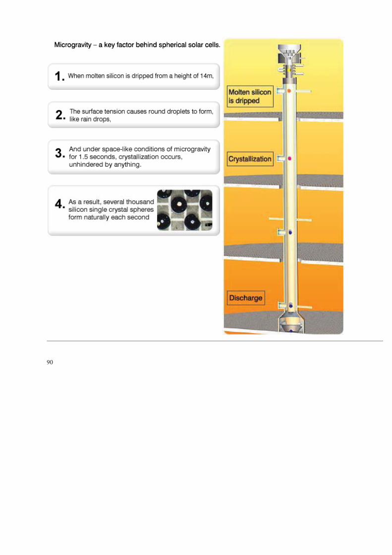
90
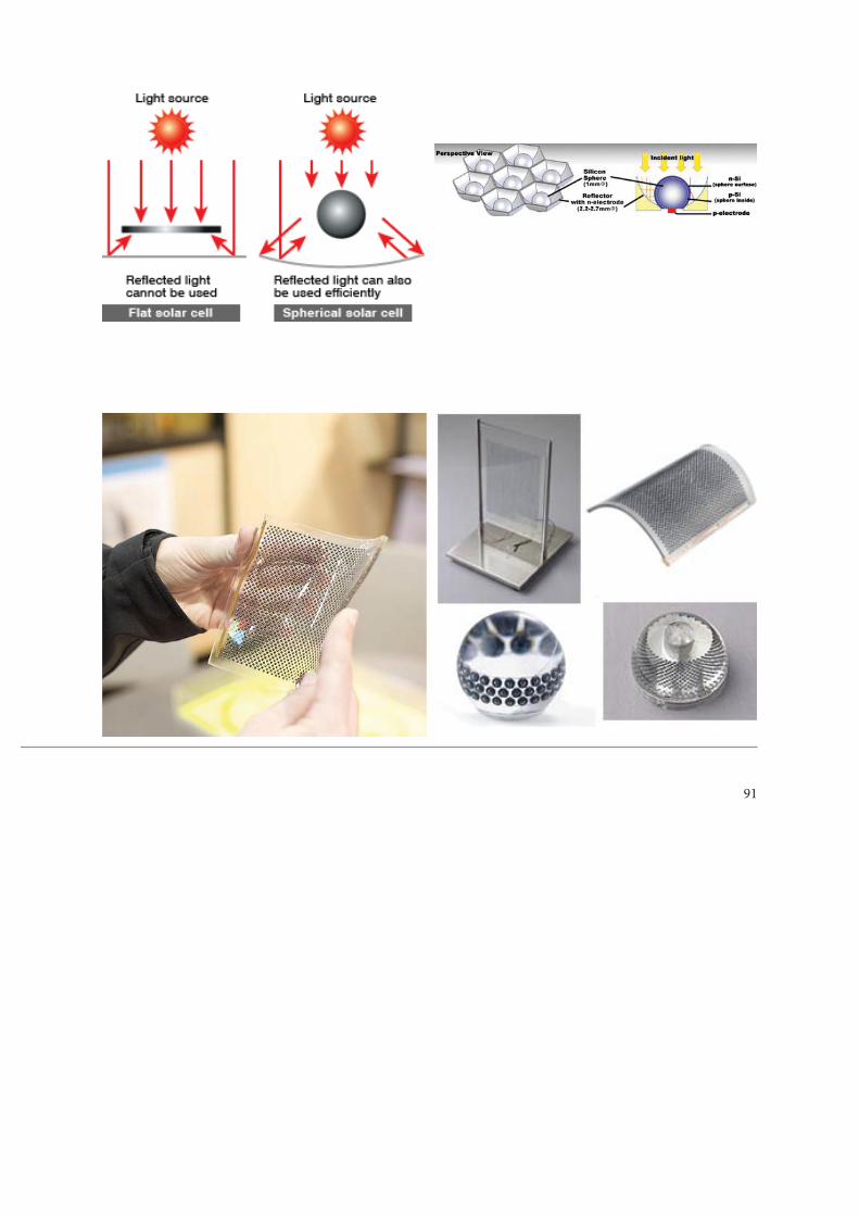
91
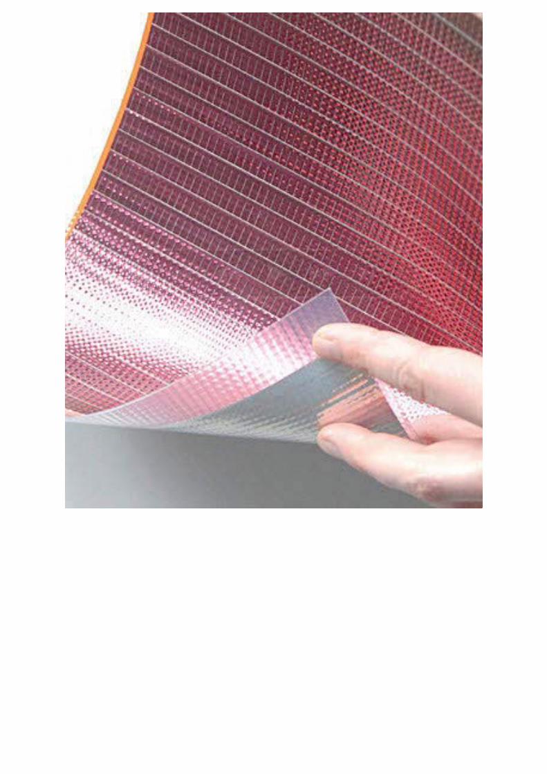
PHOTOVOLTAIC
INTEGRATED
ETFE
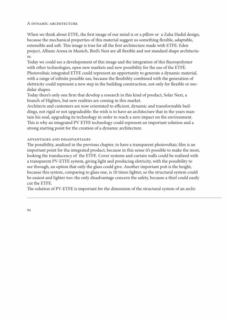
94
A dynamic architecture
When we think about ETFE, the fi rst image of our mind is or a pillow or a Zaha Hadid design, because the mechanical properties of this material suggest us something fl exible, adaptable, extensible and soft . Th is image is true for all the fi rst architecture made with ETFE: Eden project, Allianz Arena in Munich, Bird’s Nest are all fl exible and not standard shape architectu-re.Today we could see a developement of this image and the integration of this fl uoropolymer with other technologies, open new markets and new possibility for the use of the ETFE.Photovoltaic integrated ETFE could represent an opportunity to generate a dynamic material, with a range of infi nite possible use, because the fl exibility combined with the generation of elettricity could represent a new step in the building construction, not only for fl exible or mo-dular shapes. Today there’s only one fi rm that develop a research in this kind of product, Solar Next, a branch of Hightex, but new realities are coming in this market. Architects and customers are now orientated to effi cient, dynamic and transformable buil-dings, not rigid or not upgradeable: the wish is to have an architecture that in the years man-tain his soul, upgrading its technology in order to reach a zero impact on the environment. Th is is why an intagrated PV ETFE technology could represent an important solution and a strong starting point for the creation of a dynamic architecture.
advantages and disadvantagesTh e possibility, analized in the previous chapter, to have a transparent photovoltaic fi lm is an important point for tha integrated product, because in this sense it’s possible to make the most, looking the translucency of the ETFE. Cover systems and curtain walls could be realized with a transparent PV-ETFE system, giving light and producing eletricity, with the possibility to see through, an option that only the glass could give. Another important poit is the height, because this system, comparing to glass one, is 10 times lighter, so the structural system could be easiest and lighter too: the only disadvantage concern the safety, because a thief could easily cut the ETFE. Th e solution of PV-ETFE is important for the dimension of the structural system of an archi-
95
96
tecture: it’s possible to use a tenso structure or an infl ated one minimizing the use of aluminum or steel, optimizing the costs of the whole system. In particular this allows to reduce the costs of ETFE and PV. Th e ETFE for example has in the world just fi ve or six big producer, due to the complexity of the fl uorine production, and this means that costs will rise up if the production does not cover the whole demand.Th e analysis for the costs is important also for the photovoltaic fi lms: aSi fi lms are now quite cheaper, like CIGS (that are not performing a transparent panel for now), but Organic PV is expensive and the Sphelar is just under lab tests so it’s not evaluable in this moment.It is certainly important to emphasize that the maintenance of the installation is virtually nothing, because the ETFE is self cleaning and solar integrated panels, with the fi lms already described, are not so fragile like the polycrystalline type.Combining ETFE and photovoltaic fi lms there’s a material which could potentially be conside-red sustainable and producer of energy, like no other.Th e low impact on environment give the chance to be one of the most important solution in architecture in the next years. Th e solar brands are now developing a lot their technologies, preparing to substitute petrol in the supply of eletricity, with good results and new discovers. ETFE has full developed the fi lm and it’s applications, but it’s waiting a push to be more com-mercial and more diff used and known, a thing that surely could be given with the approach to the photovoltaic world.
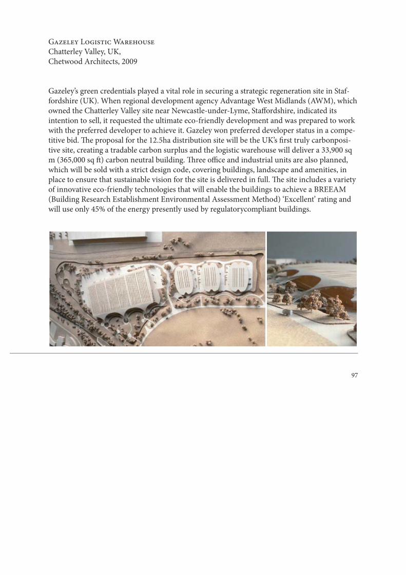
97
Gazeley Logistic WarehouseChatterley Valley, UK,Chetwood Architects, 2009
Gazeley’s green credentials played a vital role in securing a strategic regeneration site in Staf-fordshire (UK). When regional development agency Advantage West Midlands (AWM), which owned the Chatterley Valley site near Newcastle-under-Lyme, Staff ordshire, indicated its intention to sell, it requested the ultimate eco-friendly development and was prepared to work with the preferred developer to achieve it. Gazeley won preferred developer status in a compe-titive bid. Th e proposal for the 12.5ha distribution site will be the UK’s fi rst truly carbonposi-tive site, creating a tradable carbon surplus and the logistic warehouse will deliver a 33,900 sq m (365,000 sq ft ) carbon neutral building. Th ree offi ce and industrial units are also planned, which will be sold with a strict design code, covering buildings, landscape and amenities, in place to ensure that sustainable vision for the site is delivered in full. Th e site includes a varietyof innovative eco-friendly technologies that will enable the buildings to achieve a BREEAM(Building Research Establishment Environmental Assessment Method) ‘Excellent’ rating andwill use only 45% of the energy presently used by regulatorycompliant buildings.
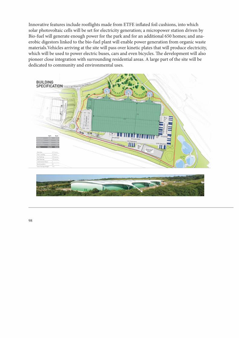
98
Innovative features include roofl ights made from ETFE infl ated foil cushions, into whichsolar photovoltaic cells will be set for electricity generation; a micropower station driven by Bio-fuel will generate enough power for the park and for an additional 650 homes; and ana-erobic digestors linked to the bio-fuel plant will enable power generation from organic waste materials.Vehicles arriving at the site will pass over kinetic plates that will produce electricity, which will be used to power electric buses, cars and even bicycles. Th e development will also pioneer close integration with surrounding residential areas. A large part of the site will be dedicated to community and environmental uses.
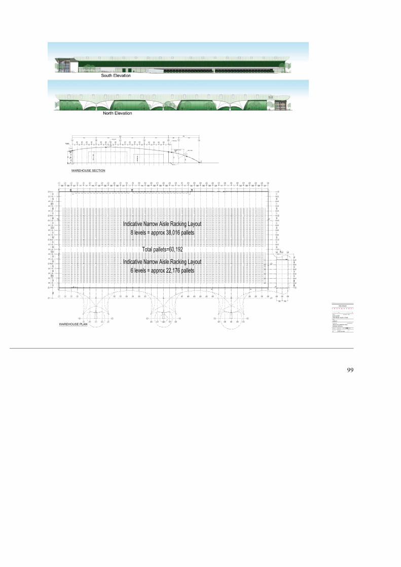
99
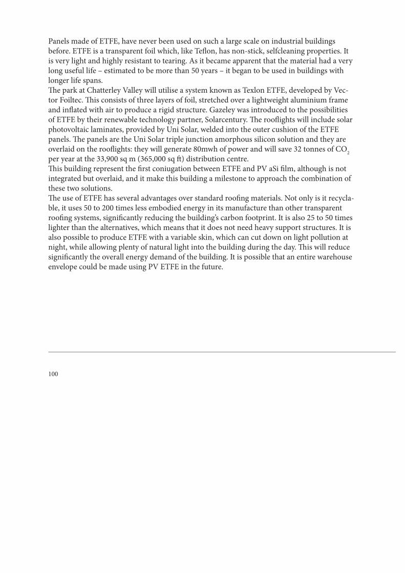
100
Panels made of ETFE, have never been used on such a large scale on industrial buildings before. ETFE is a transparent foil which, like Tefl on, has non-stick, selfcleaning properties. It is very light and highly resistant to tearing. As it became apparent that the material had a very long useful life – estimated to be more than 50 years – it began to be used in buildings with longer life spans. Th e park at Chatterley Valley will utilise a system known as Texlon ETFE, developed by Vec-tor Foiltec. Th is consists of three layers of foil, stretched over a lightweight aluminium frame and infl ated with air to produce a rigid structure. Gazeley was introduced to the possibilities of ETFE by their renewable technology partner, Solarcentury. Th e roofl ights will include solar photovoltaic laminates, provided by Uni Solar, welded into the outer cushion of the ETFE panels. Th e panels are the Uni Solar triple junction amorphous silicon solution and they are overlaid on the roofl ights: they will generate 80mwh of power and will save 32 tonnes of CO2 per year at the 33,900 sq m (365,000 sq ft ) distribution centre. Th is building represent the fi rst coniugation between ETFE and PV aSi fi lm, although is not integrated but overlaid, and it make this building a milestone to approach the combination of these two solutions.Th e use of ETFE has several advantages over standard roofi ng materials. Not only is it recycla-ble, it uses 50 to 200 times less embodied energy in its manufacture than other transparent roofi ng systems, signifi cantly reducing the building’s carbon footprint. It is also 25 to 50 times lighter than the alternatives, which means that it does not need heavy support structures. It is also possible to produce ETFE with a variable skin, which can cut down on light pollution at night, while allowing plenty of natural light into the building during the day. Th is will reduce signifi cantly the overall energy demand of the building. It is possible that an entire warehouse envelope could be made using PV ETFE in the future.
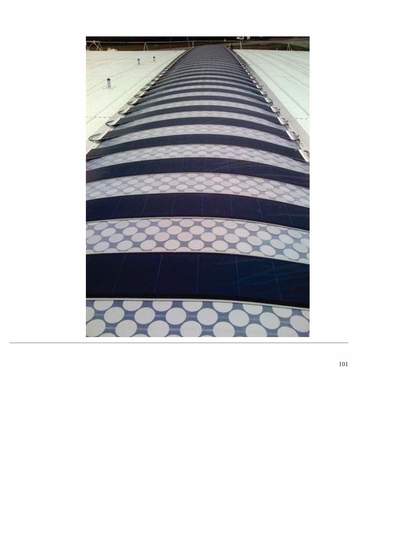
101
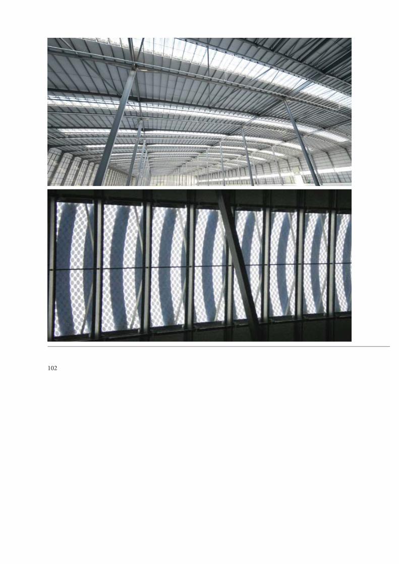
102
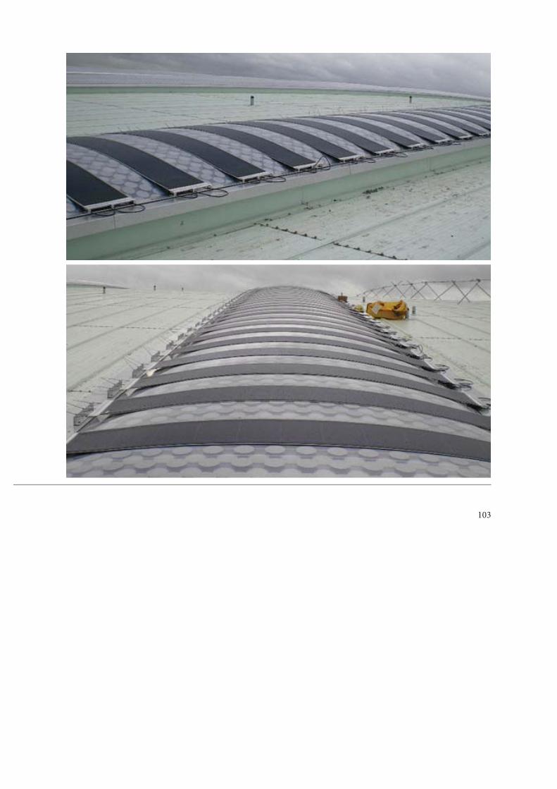
103
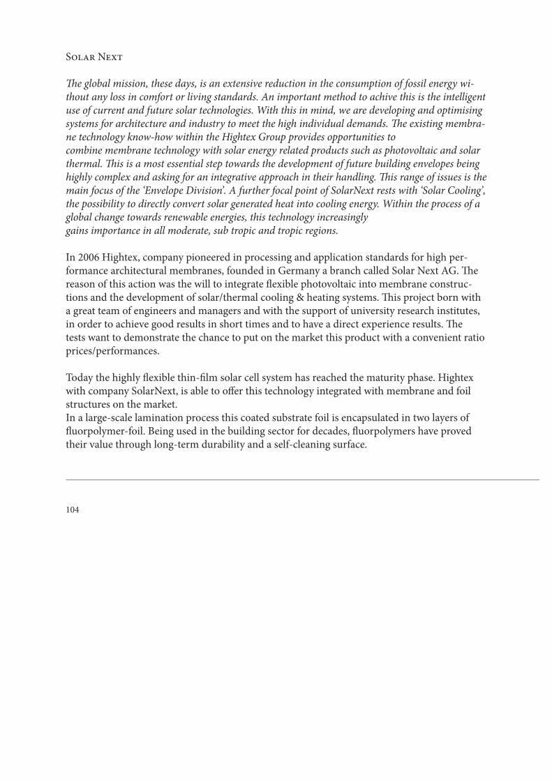
104
Solar Next
Th e global mission, these days, is an extensive reduction in the consumption of fossil energy wi-thout any loss in comfort or living standards. An important method to achive this is the intelligent use of current and future solar technologies. With this in mind, we are developing and optimising systems for architecture and industry to meet the high individual demands. Th e existing membra-ne technology know-how within the Hightex Group provides opportunities tocombine membrane technology with solar energy related products such as photovoltaic and solar thermal. Th is is a most essential step towards the development of future building envelopes being highly complex and asking for an integrative approach in their handling. Th is range of issues is the main focus of the ‘Envelope Division’. A further focal point of SolarNext rests with ‘Solar Cooling’, the possibility to directly convert solar generated heat into cooling energy. Within the process of a global change towards renewable energies, this technology increasinglygains importance in all moderate, sub tropic and tropic regions.
In 2006 Hightex, company pioneered in processing and application standards for high per-formance architectural membranes, founded in Germany a branch called Solar Next AG. Th e reason of this action was the will to integrate fl exible photovoltaic into membrane construc-tions and the development of solar/thermal cooling & heating systems. Th is project born with a great team of engineers and managers and with the support of university research institutes, in order to achieve good results in short times and to have a direct experience results. Th e tests want to demonstrate the chance to put on the market this product with a convenient ratio prices/performances.
Today the highly fl exible thin-fi lm solar cell system has reached the maturity phase. Hightex with company SolarNext, is able to off er this technology integrated with membrane and foil structures on the market.In a large-scale lamination process this coated substrate foil is encapsulated in two layers of fl uorpolymer-foil. Being used in the building sector for decades, fl uorpolymers have proved their value through long-term durability and a self-cleaning surface.
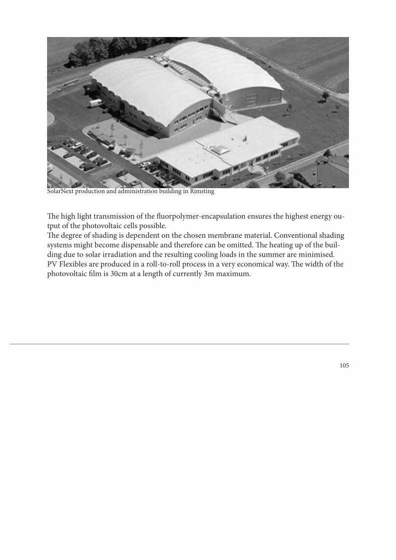
105
SolarNext production and administration building in Rimsting
Th e high light transmission of the fl uorpolymer-encapsulation ensures the highest energy ou-tput of the photovoltaic cells possible.Th e degree of shading is dependent on the chosen membrane material. Conventional shading systems might become dispensable and therefore can be omitted. Th e heating up of the buil-ding due to solar irradiation and the resulting cooling loads in the summer are minimised.PV Flexibles are produced in a roll-to-roll process in a very economical way. Th e width of the photovoltaic fi lm is 30cm at a length of currently 3m maximum.
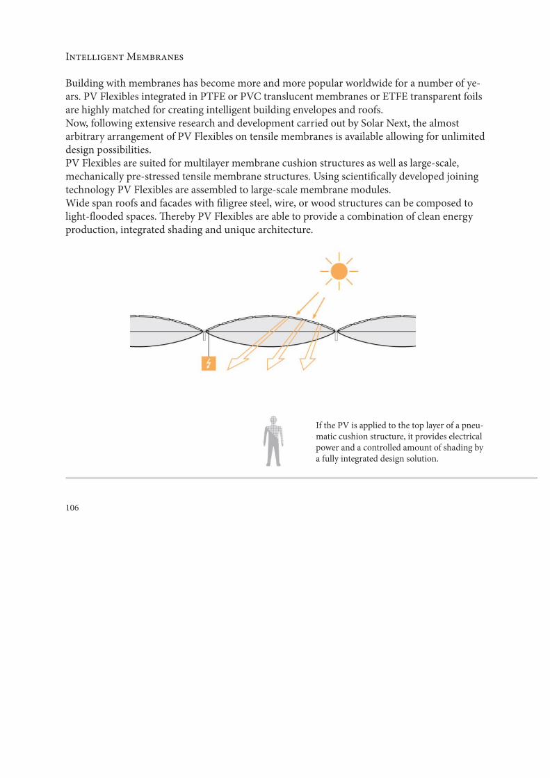
106
Intelligent Membranes
Building with membranes has become more and more popular worldwide for a number of ye-ars. PV Flexibles integrated in PTFE or PVC translucent membranes or ETFE transparent foils are highly matched for creating intelligent building envelopes and roofs.Now, following extensive research and development carried out by Solar Next, the almost arbitrary arrangement of PV Flexibles on tensile membranes is available allowing for unlimited design possibilities.PV Flexibles are suited for multilayer membrane cushion structures as well as large-scale, mechanically pre-stressed tensile membrane structures. Using scientifi cally developed joining technology PV Flexibles are assembled to large-scale membrane modules.Wide span roofs and facades with fi ligree steel, wire, or wood structures can be composed to light-fl ooded spaces. Th ereby PV Flexibles are able to provide a combination of clean energy production, integrated shading and unique architecture.
If the PV is applied to the top layer of a pneu-matic cushion structure, it provides electrical power and a controlled amount of shading by a fully integrated design solution.
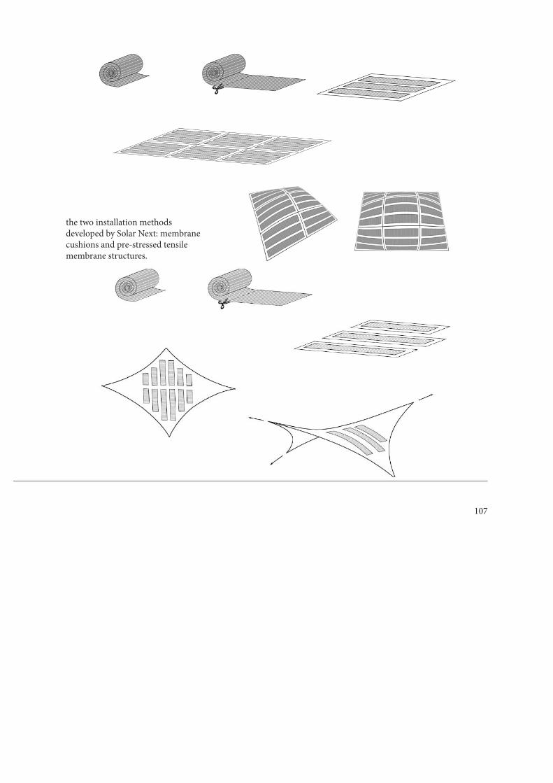
107
the two installation methods developed by Solar Next: membrane cushions and pre-stressed tensile membrane structures.
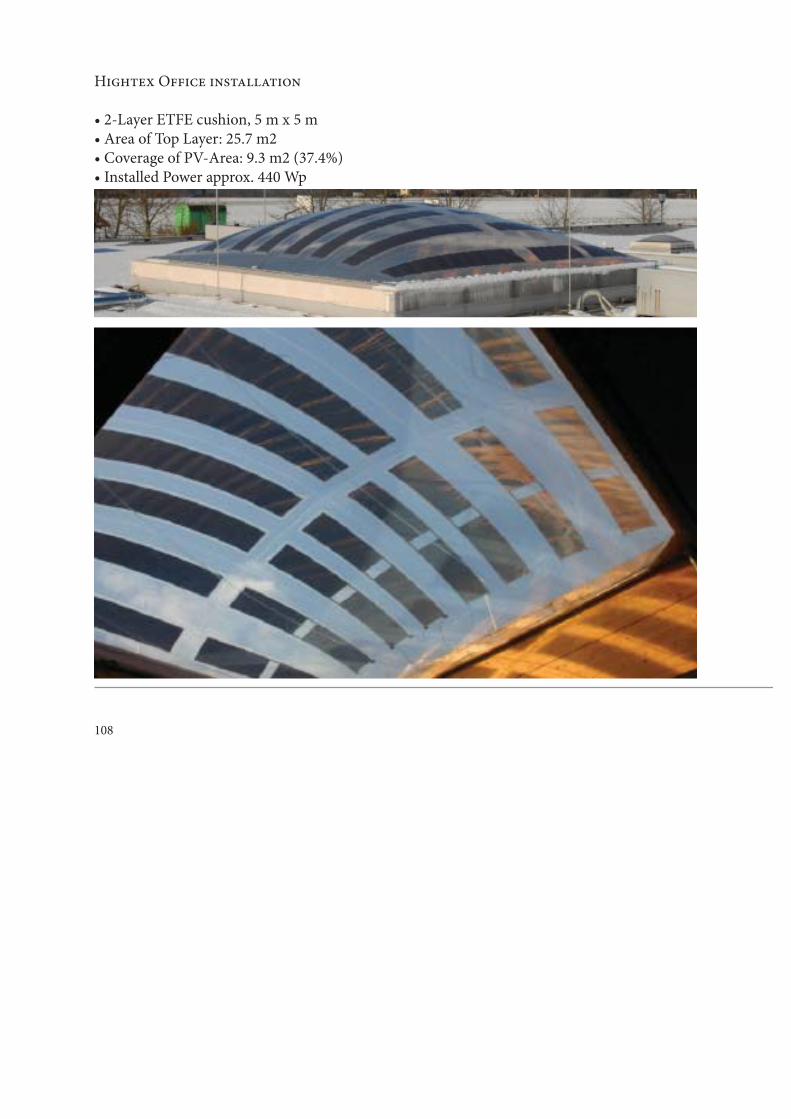
108
Hightex Office installation
• 2-Layer ETFE cushion, 5 m x 5 m• Area of Top Layer: 25.7 m2• Coverage of PV-Area: 9.3 m2 (37.4%)• Installed Power approx. 440 Wp
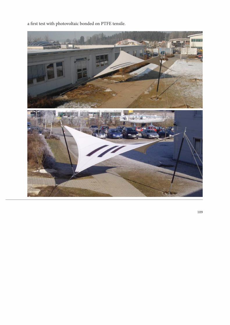
109
a fi rst test with photovoltaic bonded on PTFE tensile.
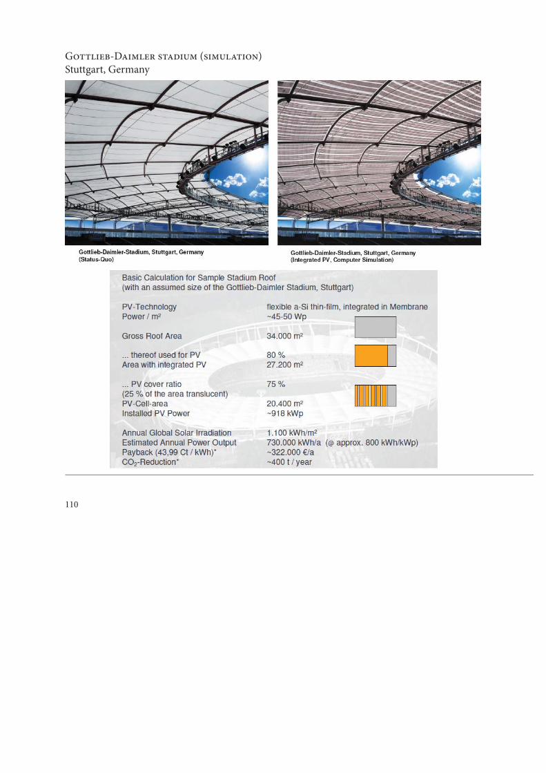
110
Gottlieb-Daimler stadium (simulation)Stuttgart, Germany
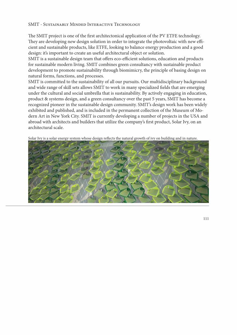
111
SMIT - Sustainably Minded Interactive Technology
Th e SMIT project is one of the fi rst architectonical application of the PV ETFE technology. Th ey are developing new design solution in order to integrate the photovoltaic with new effi -cient and sustainable products, like ETFE, looking to balance energy production and a good design: it’s important to create an useful architectural object or solution.SMIT is a sustainable design team that off ers eco-effi cient solutions, education and products for sustainable modern living. SMIT combines green consultancy with sustainable product development to promote sustainability through biomimicry, the principle of basing design on natural forms, functions, and processes. SMIT is committed to the sustainability of all our pursuits. Our multidisciplinary background and wide range of skill sets allows SMIT to work in many specialized fi elds that are emerging under the cultural and social umbrella that is sustainability. By actively engaging in education, product & systems design, and a green consultancy over the past 5 years, SMIT has become a recognized pioneer in the sustainable design community. SMIT’s design work has been widely exhibited and published, and is included in the permanent collection of the Museum of Mo-dern Art in New York City. SMIT is currently developing a number of projects in the USA and abroad with architects and builders that utilize the company’s fi rst product, Solar Ivy, on an architectural scale.
Solar Ivy is a solar energy system whose design refl ects the natural growth of ivy on building and in nature.
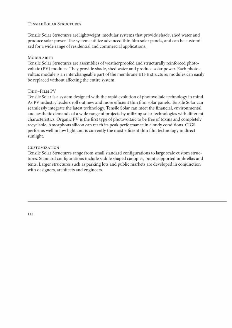
112
Tensile Solar Structures
Tensile Solar Structures are lightweight, modular systems that provide shade, shed water and produce solar power. Th e systems utilize advanced thin fi lm solar panels, and can be customi-zed for a wide range of residential and commercial applications.
ModularityTensile Solar Structures are assemblies of weatherproofed and structurally reinforced photo-voltaic (PV) modules. Th ey provide shade, shed water and produce solar power. Each photo-voltaic module is an interchangeable part of the membrane ETFE structure; modules can easily be replaced without aff ecting the entire system.
Thin–Film PVTensile Solar is a system designed with the rapid evolution of photovoltaic technology in mind. As PV industry leaders roll out new and more effi cient thin fi lm solar panels, Tensile Solar can seamlessly integrate the latest technology. Tensile Solar can meet the fi nancial, environmental and aesthetic demands of a wide range of projects by utilizing solar technologies with diff erent characteristics. Organic PV is the fi rst type of photovoltaic to be free of toxins and completely recyclable. Amorphous silicon can reach its peak performance in cloudy conditions. CIGS performs well in low light and is currently the most effi cient thin fi lm technology in direct sunlight.
CustomizationTensile Solar Structures range from small standard confi gurations to large scale custom struc-tures. Standard confi gurations include saddle shaped canopies, point supported umbrellas and tents. Larger structures such as parking lots and public markets are developed in conjunction with designers, architects and engineers.
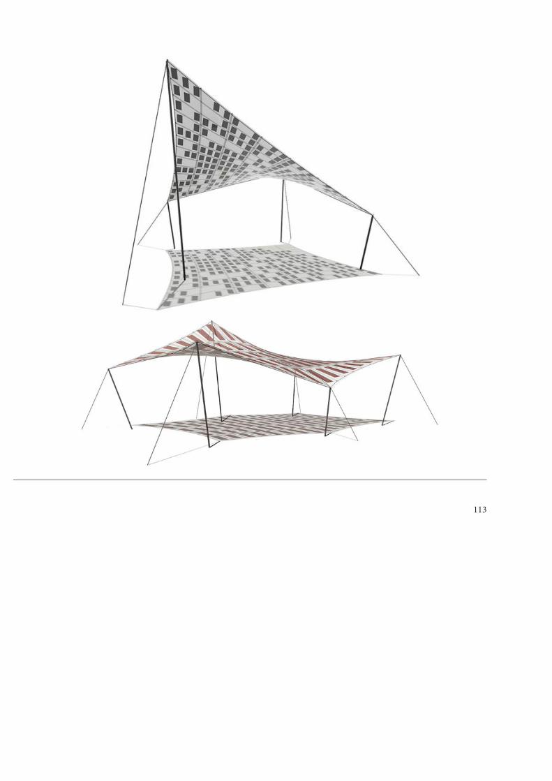
113
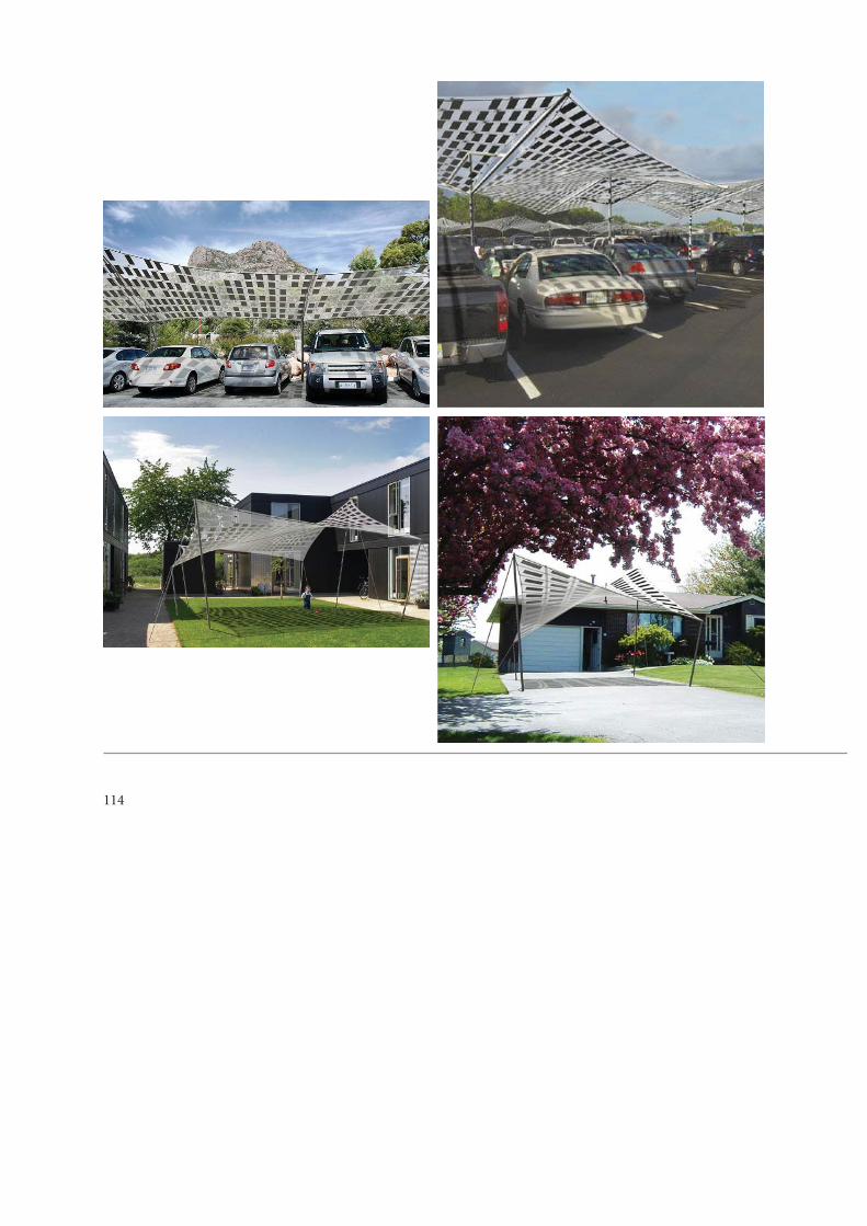
114
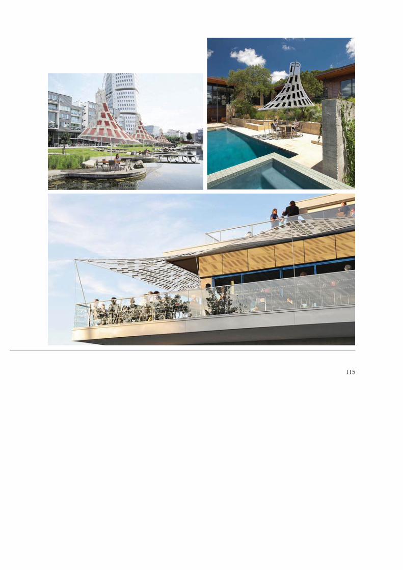
115
116
Bibliografi a
Riferimenti per le soluzioni fotovoltaiche
� Aste, Niccolò, Il fotovoltaico in architettura: l’integrazione dei sistemi a energia solare negli edifi ci, Sistemi Editoriali, 2002� Aste Niccolò, Il fotovoltaico in architettura: l’integrazione edilizia dei sistemi per la generazione di elettricità solare; aggiornato al Conto Energia (D.M. 28-7-2005), Sistemi Edito-riali, 2005� Ceccherini Nelli Lucia, Fotovoltaico in architettura, Alinea, 2006� Perago Alessandro, Progettare tetti e coperture: dalla tegola al fotovoltaico; tipologie e realizzazioni, materiali e tecniche, qualità edilizia ed effi cienza energetica, restauro, manuten-zione, bonifi ca, Maggioli, 2006� Piemontese Antonietta, Scarano Rolando, Energia solare e architettura : il fotovoltaico tra sostenibilita e nuovi linguaggi, Gangemi, 2003� P. Nath, C. Vogeli, K. Jones, A. Singh, I. Garcia, S. Guha, 28th IEEE PVSC, 2000� S. Guha, J. Yang, A. Banerjee, B. Yan, and K. Lord, Solar Energy Materials and Solar Cells, 2003� http://www.uni-solar.com/� http://www.nrel.gov/pv/highperformancepv/� http://www.nrel.gov/pv/cdte/� http://www.nrel.gov/pv/thin_fi lm/� http://www.fi rstsolar.com/environment_cdte.php� http://www.sika.it/roofi ng� http://www.solarintegrated.com/solar_tents.htm
Riferimenti per l’ETFE
� Gabriel O. Shonaike, George P. Simon - Polymer Blends and Alloys - CRC Press, 1999� Laurence W. McKeen - Fluorinated Coatings And Finishes Handbook: Th e Defi nitive
117
User’s Guide - William Andrew Inc, 2006� Philip A. Schweitzer - Mechanical and Corrosion and Resistant Properties of Plastics and Elastomers - CRC Press, 2000� Mel M. Schwartz - Encyclopedia of Materials, Parts, and Finishes - CRC Press, 2002� Tony Whelan - Polymer Technology Dictionary - Springer, 1994� J. A. Brydson - Plastics Materials - Butterworth-Heinemann, 1999� Giuseppe Frigione, Nicoletta Mairo - Materiali per l’edilizia. Una guida ai materiali strutturali, ausiliari e di rivestimento - Hoepli Editore, 2006� http://www.fl uon.jp/� http://www2.dupont.com/Plastics/en_US/� http://www.vector-foiltec.com/vector.htm� http://www.ceno-tec.de/� http://solutions.3m.com/wps/portal/3M/en_US/dyneon_fl uoropolymers/Home/� http://www.hightexworld.com/page/index.html
Riferimenti per ETFE Fotovoltaico
� http://www.solarnext.eu/htmlEng/kontakt.html

118

119