Embed Size (px)
Citation preview

A Theoretical Analysis of the Current-Voltage
Characteristics of Solar Cells
Annual Report on
NASA Grant NGR 34-002-195
June 1974
J. R. Hauser and P. M. Dunbar
Reproduced by
NATIONAL TECHNICALINFORMATION SERVICE
US Department of CommerceSpringfield, VA. 22151
Semiconductor Device LaboratoryDepartment of Electrical Engineering
North Carolina State UniversityRaleigh, North Carolina 27607
(NASA-CR-138828) a THEORETICAL ANALYSIS N74-28544
OF THE CURRENT-VOLTAGE CHARACTERISTICS OF
SOLAR CELLS Annual Report (NorthCarolina State Univ.) Unclas
CSCL 10A G3/03 54111
https://ntrs.nasa.gov/search.jsp?R=19740020431 2018-08-31T19:47:13+00:00Z
ABSTRACT
This report summarizes work to date performed under NASA Grant
NGR 34-002-195, entitled A Theoretical Analysis of the Current-Voltage
Characteristics of Solar Cells. The objective of the research is to
provide a theoretical understanding of the operation of solar cells
so they can be designed for maximum efficiency, These objectives are
being pursued through the application of a general computer device
analysis program to the study of solar cell properties, During the
past twelve months considerable progress has been made toward these
objectives. Specifically an analysis program for solar cells has been
developed which provides for non-uniform doping profiles, generation-
recombination effects, field and doping dependent mobility, and optical
generation. Preliminary results with the analysis program indicates
that the predicted efficiencies agree reasonably well with experimental
efficiencies for silicon solar cells.
This report summarizes the major work to date on the current-
voltage characteristics and efficiencies of.solar cells. For one solar
cell structure detailed curves are presented which include carrier
densities, current densities, potential, and quasi-Fermi levels at
different voltage levels both with and without optically generated
carriers (AMO conditions). In addition some results are presented
concerning the influence of various parameter variations such as
lifetime, cell thickness, and high-low junction width on solar cell
performance. 0
/

I. COMPUTER ANALYSIS PROGRAM
A considerable part of the effort during this first year's
research has been devoted to adapting a computer device analysis
program to the analysis of solar cells. The present computer
analysis program is able to account for the following physical effects
in a semiconductor device:
1. Drift and diffusion currents
2. Non-uniform doping profiles
3. Bulk generation-recombination effects
4. Field dependent and doping dependent mobility
5. Optical carrier generation
6. Surface recombination
The effects above which have been included in the analysis program
during the present research work are non-uniform doping profiles,
optical carrier generation, and surface recombination.
Two papers have been prepared for submission for publication.
One of these discusses the computer analysis program and the mathematical
techniques used to solve the nonlinear semiconductor device equations,
while the other discusses the studies which have been carried out on
optical carrier generation and the effects of antireflecting layers on
optical carrier generation in silicon. Copies of these manuscripts are
included in Appendices A and B. These provide detailed summaries of
the work performed on developing the computer analysis programs.

2
II. DETAILED CHARACTERISTICS AND PROPERTIES OF+ +n -p-p SOLAR CELLS
A considerable number of detailed calculations have been made of the
electrostatic potential, quasi-Fermi levels, carrier densities, and current
densities in solar cells. Both the conventional n -p cell and the back
+ +surface field (or high-low junction) n -p-p cell, as shown in cross
section in Figure 1, have been analyzed. More effort has been directed
toward the n -p-p structure than the conventional cell because of
+ +questions concerning the enhanced efficiency of the n -p-p cell.
Since the device analysis program solves for the internal potential
and quasi-Fermi levels; it provides a detailed look at the internal
operation of the solar cell. A large amount of data is generated on each
device studied. The results presented in this section show detailed
internal characteristics for one particular solar cell under both conditions
of no illumination and under the full solar spectrum illumination (AMO).
Material and dimensional properties of the device for which detailed plots
are presented are given in Table I. The lifetime of 100 psec in the
Table I. Material and dimensional properties
Overall cell thickness - 250 pM
n thickness - 0.25 uM
p thickness - 0.50 UM
n surface concentration - 1020/cm3
p doping concentration (10 0°cm) - 1.3x10¹⁵/cm 3
p doping concentration - 1018/cm3
minority carrier lifetime no 100 psec
To - 0.1 psecpo

3
p-region corresponds to a diffusion length of about 588 pM or a little
more than twice the cell thickness, The first sequence of Figures 2-8
show the device characteristics without illumination. Figure 2 shows
the electrostatic potential across the device with 2(a) showing the
entire device length while 2(b) and 2(c) shows expanded views about
the p-n+ and p -p junctions respectively. The various curves correspond
to applied voltages ranging from 0.1 to 0O7 volts. The expanded views
are needed to see details about the junctions because of their small
thickness. Of special interest in this figure is the reduction in
potential across the high-low junction as seen in Figure 2(c) for
large values of applied voltage. This reduction begins to occur when
the minority carrier density exceeds the doping in the p-region, i.e.
when high injection occurs.
Figures 3(a), 3(b), and 3(c) show complete and expanded plots of
electron quasi-Fermi level in the device. The expanded plots illustrate
that the quasi-Fermi level is essentially constant across both junction
space charge regions as is assumed in most first order analytical device
calculations. This first order assumption is not made in this calculation
but it is seen that relatively constant quasi-Fermi levels in the space
charge regions do in fact result. The major feature of these plots is
the almost abrupt change in #0 as seen in Figure 3(c) at the high-lown
junction. This change in slope is required because of the essentially
constant current density across the high-low junction coupled with the
large change in electron density across the high-low junction.
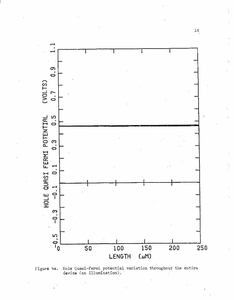
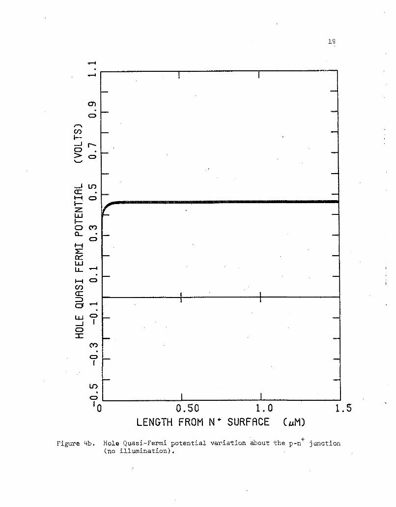
Figure 4(b) shows the hole quasi-Fermi level around the p-n junction.
Plots for the p-p junction are not shown since p is essentially

constant in this region as seen from Figure 4(a). Changes in p
only occur very near the surface, and these large changes only occur
because of the value of surface recombination used in the calculations
(infinite value used).
Figures 5(a), 5(b), and 5(c) show electron concentration for the
complete device and expanded views near the two surfaces for various
applied voltage values. The large changes in carrier density across
the high-low junction as seen in Figure 5(c) illustrate the minority
carrier reflecting properties of the high-low junction. The log scales
used to plot electron density are needed to cover the large range of
densities encountered as the applied voltage ranges from 0.1 volt to
0.7 volt; however, these log scales tend to distort somewhat the
carrier density plots. For example the electron concentrations in the
p region as shown in Figure 5(c) from 0 to 0.5 pM vary approximately
linearly with distance. This linear variation plots on a log scale
as a very rapidly varying function near zero and a slowly varying function
as 0.5 vM is approached. The very rapid decrease in electron concentration
near the back contact is due to the assumption of an ohmic contact. This
does not allow the carrier density to increase from its equilibrium value
which is slightly above 102/cm3 . The change in electron concentration
across the high-low junction is related to the high-low junction potential
as
S+ = np exp(-qVhl/kT). (1)
The high-low junction potential is given as
kT N +Vh = £n ( + n . (2)S q N pp
p

5
The combination of Eqs. (1) and (2) gives
N n
n = n -- ( + ). (3)p pN+ N
This relationship, as discussed in Appendix C, is followed very accurately
for the high-low junctions analyzed in this work,
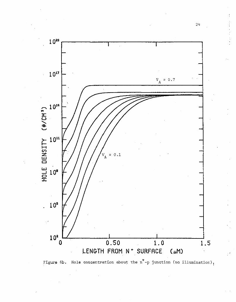
Hole concentration curves are shown in Figures 6(a), 6(b), and 6(c)
for both the complete device and expanded views about the two junctions.
The hole density in the center of the device is seen to be constant and
essentially independent of applied voltage except for the highest
voltage values which correspond to high injection in the center p-region.
Of special interest are the hole densities in Figure 6(c) for the
n+ surface region. This illustrates the injection of holes into the
n+ region (x<0.25 PM). The hole density exhibits a rapid decrease near
x=O due to the large surface recombination velocity assumed at the surface.
For low values of surface recombination the hole density will not be forced
to the low values (below 102/cm3) shown in Figure 6(c).
Electron and hole current densities as functions of distance at the
various applied voltage values are shown in Figures 7 and 8. In this case
expanded views are shown only for the surface n -p junction since the
current densities are essentially constant through the p region. As can
be seen in Figures 7(b) and 8(b) at low forward voltages there is a large
change in current density in the vicinity of the n -p junction
(x < 0.5 PM). This occurs because a large part of the current density
consists of recombination current from within the junction depletion
region at low applied voltages.

6
A set of curves similar to those of Figures 2-8 are shown in
Figures 9-15 for the same solar cell structure but including pair
generation due to AMO illumination. The assumed surface condition is
that of a polished surface with no antireflecting layer but reflection
from the surface is taken into account. For this sequence of figures,
the terminal voltage ranges from 0.6 volt to 0.0 volt with curves shown
for 0.1 volt steps. The irradiated surface is at x = 250 pM. The
open-circuit voltage condition occurs between the 0.5 volt and 0.6 volt
curves. For all curves except the current density curves, the curves
do not exhibit any unusual features near the open-circuit voltage
condition.
The electrostatic potential curves of Figure 9 are for all practical
purposes identical to those of Figure 2 in the absence of illumination.
The potential distribution within the device is determined by the terminal
voltage and is independent of the optical illumination.
The variation-in the quasi-Fermi level can best be illustrated in
conjunction with the carrier density curves. The illumination produces
an excess electron and hole density which is quite evident in Figures 12 and
13. This excess carrier density is also indicated by the shift of the quasi-
Fermi potentials. This shift is most evident for electrons in the p-region
+(0n of Figures 10(a) and 10(b)) and holes in the n region (4p of
Figure 11(b)). At lower bias the electron concentration in the p-region
(Figure 12(a)) is greatly reduced near the n -p junction due to the
collection of the electrons by this junction yielding the short circuit
current. It can be noticed, however, from Figure 12(b) that the decrease
in electron concentration near the junction is limited by the saturation

7
drift velocity. The minimum electron density of around 2 x 10¹⁰/cm 3
(near x = 0.5 PM in Figure 12(b)) is needed at the saturated carrier
drift velocity to support the collected photocurrent. This is also
present in Figure 13(b) which indicates that the saturation velocity
is reached for holes. This is seen as the fairly flat region of hole
density below x = 0.5 rM. The surface variation of pn+ and p , in
Figures 13(b) and 11(b) also indicate the directional change in Jp due
to surface recombination. The collection of the optically generated
holes is evidenced by the small reverse curve in Figure 13(b) for
voltages less than 0.4 v. Had velocity saturation not set in this
would have been a much deeper curve. It is none the less quite evident
that first order diffusion methods cannot properly model the case of
high optical currents.
The effects of the various :aturation mechanisms point out the
need for future calculations to include the full generation term instead
of the present methods of scaling up the results from the case of lower
generation due to the absence of an antireflection layer. Included in
these effects is that of high injection due to the carriers. It can be
seen from Figure 12(a) that high injection (due to optical generation
alone) is approached in the bulk p-region as the electron density
approaches 1013/cm3. For the situation of higher bulk generation rates
it is quite likely that the high injection condition in the bulk would
be met. Among.other things this would alter the reflecting characteristics
of the high-low junction. These conditions of drift velocity saturation
and high injection could have significant effects on the terminal
characteristics which would not be evident from calculations based alone
on the lower generation rates.

The current density curves of Figures 14 and 15 are, as before,
plotted in terms of absolute magnitude. The dips in these curves are in
fact directional changes so the current does pass through zero at these
points. There is no directional change in electron current for high
bias (Va = 0.6 v, Figure 14(a)) due to the overriding effect of the
forward p-n junction current. At lower bias however, the predominant
electron current consists of collection of optically generated carriers
by the p-n+ junction. The 0.5 v curve in Figure 14(a) represents a
transitional region around the open circuit condition. For situations
where the effective surface recombination velocity of the high-low
junction is much lower,.it has been observed that the directional change
due to carriers supporting back contact recombination occurs much
closer to the high-low junction than that illustrated in Figure 14(a).
The hole current density of Figure 15 illustrates a similar
transitional curve but at a higher bias voltage (0.6 v) due to the lower
forward pn junction hole current. The current lost due to surface
recombination is quite evident from Figure 15(b), where a reversal of
the current direction near the surface indicates current flow to the
surface due to surface recombination. Realize that for the lower bias
(less than 0.6 v) the predominant hole current consists of the optical
component (except at the surface).
The terminal characteristics of this solar cell are shown in
Figures 16, 17 and 18. The J-V characteristic in the absence of light
is shown in Figure 16. This curve is typical of most silicon diodes.
At voltages ranging from about 0.35 volt: to about 0.55 volt the current
density varies approximately as exp(qV/kT). At lower and higher voltages
the current changes less rapidly with voltage approaching the approximate

9
variation of exp(qV/2kT). The deviation from ideal behavior at low
voltages arises from recombination of carriers within the junction
depletion region while the high voltage deviation occurs because of
high injection into the p-region.
The terminal J-V characteristic under illumination is seen in
Figure 17. From this the short circuit current is seen to be about
34 ma and the open circuit voltage about 0.58 volt. The efficiency
vs voltage characteristic is seen in Figure 18 where the peak efficiency
is slightly below 12%. This is the calculated efficiency without an
antireflecting layer, The efficiency of such a cell with an anti-
reflecting layer would be expected to be about 40% larger or between
16% and 17%. This calculated efficiency is significantly larger than
that observed in commercial 10 0*cm solar cells. There are several
possible reasons for this. First the lifetime of 100 psec used in the
p-region may be larger than that obtainable in present solar cells.
Lifetime values of 10 psec have frequently been quoted as typical
lifetimes in 10 n-cm solar cells. Calculations for lower lifetime
cells are given in the next section. The lifetime of 0.1 psec used
in the n region may again be larger than actually obtained in commercail
cells. However, very small values of lifetime are required in the n+
layer to significantly reduce the efficiency because of the very thin
n+ region. It was also found that the calculated generation rate used
in-the presented data was about 10% high. As a result of this the
efficiency results actually lie between that of a bare surface and that
with a ieflecting layer. Including this factor would lower the efficiency
for the.cell .ith the antireflecting layer to between 15 and 16%. The
optical generation parameter presented in Appendix B represent the
corrected generation rate.
10
There are other effects which may reduce the efficiency in real
solar cells. The ohmic resistance due to a two-dimensional contact
geometry reduces the curve factor decreasing the efficiency. Also
heavy doping (degeneracy) effects in the emitter are not accounted
for. These effects can enhance the loss of carriers at the surface
and decrease the efficiency. These effects are to be incorporated
into the theoretical analysis during the continued research work.

Light
p
a. Conventional p-n solar cell
i Light
n
p
p
+ +b. Back surface field, p -p-n solar cell
Figure 1. Device structure utilized in the theoretical analysis.

12
CD
C)
CD
O0
--
o5.-
dCr) C
-
LJ V 0.1 to 0.5-j AUJ
- 0.6
'0 50 100 150 200 250LENGTH (AM)
Figure 2a, Electrostatic potential variation throughout the entiredevice (no illumination).

13
S V = 0.1a A
Co)
I--J
0
F1
u-
0-
F-
-J
C:) VA = 0.7
'0 0.50 1.0 1.5LENGTH FROM N " SURFACE (uM)
Figure 2b. Electrostatic potential variation about the p-n junction(no illumination).

14
Oc)C\J
VA = 0.1 to 0.5
) -0.6
-
I- *
0.7
C-)
-
C)
O I
u-
0 0.50 1.0 1.5LENGTH FROM P SURFACE (uM)
Figure 2c. Electrostatic potential variation about the high-lowjunction (no illumination).

15
LI)
S I
V = 0.1
CAI-'
_j
--J
z
I-.
CDF-
o I I I I0 so50 100 150 200 250
LENGTH (uM)
Figure 3a. Electron Quasi-Fermi potential variation throughout theentire device (no illumination).

16
O
V 0.1
-J
CD
CV
O
C0 VA = 0.7
U,
-J
0 0.50 1.0 1.5LENGTH FROM N* SURFACE (MM)
Figure 3b. Electron Quasi-Fermi potential variation about the p-njunction (no illumination).
3 -:
o.."
/rV .
junction (no illumination).

17
U-
V = 0.1
F-1
C)
O
C
L.
_J
LO)
'0 0.50 1.0 1.5
LENGTH FROM P SURFACE (.M)
Figure 3c. Electron Quasi-Fermi potential variation about the high-low
junction (no illumination).
18
C,)
I-
CO
_J
> o
U
OCD09
LLU
- I I I I
CDI I
'0 50 100 150 200 250LENGTH (uM)
Figure 4a. Hole Quasi-Fermi potential variation throughout the entiredevice (no illumination).
19
r)
->CD *JLF
co
C)C0
LLJ.
CO
I
O
C)
IO
10 0.50 1.0 1.5LENGTH FROM N" SURFACE (uM)
Figure 4b. Hole Quasi-Fermi potential variation about the p-n+ junction(no illumination).

20
1020
10L7V = 0.7
S10"11
o
0
>-
VA = 0.1LJ
10s
102 I I I I
0 50 100 150 200 250LENGTH (uM)
Figure 5a. Electron concentration throughout the entire device(no illumination).

21
1020
10 17VA =0.7
>--
VA = 0.1
10102
102. I I0 0.50 1.0 1.5
LENGTH FROM N* SURFACE (uM)
Figure 5b. Electron concentration about the n -p junction(no illumination).

22
1020
10 -VA =0.7
" 10"
S10 •C-)
VA = 0.1
10s
102
0 0.50 1.0 1.5LENGTH FROM P* SURFACE (CuM)
Figure 5c. Electron concentration about the high-low junction(no illumination) .

23
1020
1017VA = 0.7
VA = 0.6
VA = 0.1 to 0.5
1014 -
>- 1011 -I--
Cr)
105 -j 108
102 I I I I0 50 100 150 200 250
LENGTH (uM)
Figure 6a. Hole concentration throughout the entire device(no illumination).
24
1020
VA= 0.7
10k1
>- 10"I--
C/)
Z VA 0.1a--LUJ
-J 10'0
1020 0.50 1.0 1.5
LENGTH FROM N* SURFACE (uM)
Figur.e 6b. Hole concentration about the n -p junction (no illumination)t

25
1020
107 vA = 0.7V = 0.6
VA = 0.1 to 0.5
10 -
> 10"
C-
- 108
C)
1 058
102 I I
0 0.50 1.0 1.5LENGTH FROM P* SURFACE (uM)
Figure 6c. Hole concentration about the high-low junction(no illumination).

26
100
101 -- VA = 0.6
I-'
'a1
-t
ZCO
10
C10)LU
106V = 0.3
10 -
10-0 50 100 150 200 250
LENGTH (uM)
Figure 7a. Electron Current density variation throughout the entiredevice (no illumination).

27
100
I-
10-210'
LU
U 10-2
O-
1 10-6
0
Uj 1 0 --
10-70 0.50 1.0 1.5
LENGTH FROM N* SURFACE (uM)
Figure 7b. Electron current density variation about the n -p junction(no illumination).

28
V = 0.7
100
" 10
>_ 10-
10 "
-J
10-6
104 --------
V = 0.2A
10-10 50 100 150 200 250
LENGTH (uM)
Figure 8a. Hole current density variation throughout the entiredevice (no illumination).

29
10 II
1 0-1
V = 0.7
>- 10-2I-I-I
CD
UJ
-
10 -7
V = 0.2
0 0.50 1.0 1.5LENGTH FROM N' SURFACE (UM)
Figure 8b. Hole current density variation about the high-low
junction (no illumination).

30
O
-
LO
C)
Co
>I
-
a-
I-
as
O i
LaJ
LENGTH (uM)
't-
device (AM0 illumination). '

31
C-)
-
C)cD
-J
0_>
i--
F- VA = 060.0
(AMO illumination).
C-3
I-
LJV 0.6
'0 0.50 1.0 1.5LENGTH FROM N* SURFACE (.lM)
Figure 9b. Electrostatic potential variation about the p-n junction(AMO illumination).

32
OC>
I I
VA : 0.0 to 0.5
C -VA =0.6
J
CLD
C-O
F-
O .C,
LI)
UuJ
0 0.50 1.0 1.5
LENGTH FROM P* SURFACE CrM)
Figure 9c. Electrostatic potential variation about the high-lowjunction (AMO illumination).

33
-J
-O
CE
C)
LL -4 VA= 0.5O
0 V A 0.0 to 0.4
U: V = 0.6
-1 A
C)
o I I I
'0 50 100 150 200 250LENGTH (uM)
Figur 10a, Electron Quasi-Feri on ~l varition throughout theentire device (AMO illumination).
M
CD

34
VA 0.0
U)
4-ec
.J
CD
0-O
LI
SVA o6
O
:)
C
L0
o
0 0.50 1.0 1.5LENGTH FROM N' SURFACE (uM)
Q1-
Figure 10b. Electron Quasi-Fermi potential variation about the p-njunction (AM0 illumination).

35
LO
C)
_J
C- VA =0.0 to 0.4-rI
0")
SV A 0.6
C)
LLJ
-JLUL
0 0.50 1.0 1.5
LENGTH FROM P"' SURFACE (MM)Figure 10c. Electron Quasi-Fermi potential variation about the high-low
junction (AMO illumination).

36
C)
O
I-
I-O CO
CO
c,
a I I I
LENGTH M)
Figure 11a. Hole Quasi-Fermi potential variation throughout theentire device (AM0 illumination).
a:n 01010 0 5
OfGT (M
LLJ C .Hl ~as-em otnilvrito houhu hC)iedvo(MOilmnto)

37
C)f-
* V 0.0> 3 A
- V = 0.6
O CY)LL.
II
LO
UJr
LENGTH FROM N' SURFACE (uM)
tion (AMO illumination)
CO
10 0.50 1.0 1.5LENGTH FROM N* SURFACE (MM)
Figure Ilb. Hole Quasi-Fermi Potential variation about the p-njunction CAMO illumination).

38
1020
1017
VA = 0.6
" 10 1 - vA = 0.s
V = 0.0 to 0.4A
015
C-
"; 108__)
10
0 50 100 150 200 250
LENGTH CM)
Figure 12a. Electron concentration throughout the entire device(AMO illumination).(AMO illumination).

39
1020
1017
VA= 0.6
10" -
- 10 11 v = .
0-102 VA 0L--
0 0.50 1.0 1.5LENGTH FROM N* SURFACE (CM)
+
Figure 12b. Electron concentration about the n -p junction(AMO illumination).

40
1020
1017
VA = 0.6
S101 v = 0.5
S= 0.0 to 0.4A
>-
O
1011
C,)
-J
105
102I I0 0.50 1.0 1.5
LENGTH FROM P. SURFACE (uM)
Figure 12c. Electron concentration about the high-low junction(AMO illumination)?.

41
1020
1017
VA = 0.6
V = 0.0 to 0.5
> 1014
>- 1ll
CO
H
10" -
C)
105
102 I I I I0 50 100 150 200 250
LENGTH (uM)
Figure 13a. Hole concentration throughout the entire device (AMOillumination).

42
1020
100
VA = 0.6
1011-
V 0.0AA
> 101
(O-
0*)
-1 108-"
10s
102 I I0 0.50 1.0 1.5
LENGTH FROM N' SURFACE (uM)
Figure 13b. Hole concentration about the n -p junction(AMO illumination).

43
1020
1017
VA= 0.6
- VA = 0.0 to 05A
C10 -
Li'
J 10 -
10s
102 I I0 0.50 1.0 1.5
LENGTH FROM P' SURFACE (MM)Figure 13c. Hole concentration about the high-low junction
(AMO illumination).

10,
10- - VA 0.6
A
0 10 -
-VA = 0.0 to 0.4
S 10 - V 0.s
0 -
10C -
.J
106
i -
10 I I I I0 50 100 150 200 250
LENGTH (uM)
Figure 14ao Electron current density variation throughout the entire
device (AMO illumination).

45
100
10 - v = 0.6
V = 0.0 to 0.4LA
V = 0.5A
-I 10-2
I-
S10-
z
U--..J
106-
10-7 I I0 0.50 1.0 1.5
LENGTH FROM N' SURFACE (.M)
Figure 14b. Electron current density variation about the n -p junction(AMO illumination).

46
100
10 -
VA = 0°0 to 0.5
'-A
I -
" 10 -
V =06
CO
LU
10 -
10 I I
0 50 100 150 200 250LENGTH (M)
Figure 15a. Hole current density variation throughout the entiredevice (AMOillumination).

47
100
VA = 0.0 to 0.5
V= 0.6A
>- 10
C-
m, 10
-J
CD
10 - 6 .
10-
0 0.50 1.0 1.5LENGTH FROM N' SURFACE (uM)
Figure 15b, Hole current density variation about the high-lowjunction (AMO illumination).

100
a 10-
10 -
II
0.2 0.3 0.4 0.5 0.6 0.7
C,)
eL
F--J
I--I
0.2 0.3 0.4 0.5 0.6 0.7VOLTAGE (VOLTS)
Figure 16o Terminal J-V characteristics of the n -p-p solar cellunder no illumination.

Ir I I I I I I
CD
-0k- E
I--
CO
LJ
± +
Figure 17. Terminal J-V characteristics of the n -p-p solar cell under AMO illumination.
-4ZtO

50
tII CI
CO)Z o
C-
00
I I 1 ! I0.1 0.2 0.3 0.4 0.5 0.6 0.7
VOLTAGE (VOLTS)+ +
Figure 18. Efficiency characteristics of the n -p-p solar cell (AMOillumination).

51
III. EFFECT OF HIGH-LOW JUNCTION ON SOLAR CELLPROPERTIES AND EFFICIENCY
In addition to developing a solar cell analysis program, one
of the major efforts during this year's research has been the
attempt to better understand the role of a p -p or high-low junction
at the back surface of a solar cell. In general, the computer
calculations have shown that the first order models for high-low
junction behavior are very closely satisfied by the junctions studied
in this work. A comparison of the numerical results with first order
high-low junction equations is given in Appendix C.
The high-low junction has been found to act at low voltages
primarily as a minority carrier reflecting back contact giving a small
effective surface recombination velocity at the boundary of the p-p+
junction. The curves of electron concentration in Figure 5 show the
large change in electron concentration occurring at the high-low
junction.
Several calculations have been made to explore the effect of a
back surface high-low junction on overall efficiency. Figures 19, 20
and 21 show one series of modifications of the back p contact.
Curves are shown for three devices: (a) ohmic back contact, (b) 0.5 pM
thick back p region and (c) 5 pM thick back p region. Other parameters
for the devices are as given in Table I. Figure 19 shows a very
significant decrease in the current density at a constant voltage for
the devices with p+ back contacts. The decrease in current is due to
the decreased flow of injected electrons to the back ohmic contact.
The 5 UM p+ device shows only a slight improvement over the 0.5 PM device.

52
The 5 pM and 0.5 iM devices have back boundary effective surface
recombination velocities of 1.1 cm/sec and 204 cm/sec respectively.
The value for the 0.5 UM device is already so low that it acts almost
as an ideal minority carrier reflecting back contact.
The current density vs voltage characteristics for the three
devices are shown in Figure 20. The ohmic back contact device is
seen to have a reduced short circuit current and a reduced open
circuit voltage. The reduced short circuit current arises from the
loss of optically generated carriers at the back contact. The
reduced open circuit voltage arises from the combined effects of a
smaller photocurrent and a larger forward diode current as indicated
in Figure 19. The efficiency curves of Figure 21 illustrate the
improved efficiency of the high-low junction solar cell. There is
little change in peak efficiency between the 0.5 pM and 5 pM cells.
Calculations similar to those described above were also made for
250 pM thick devices with 10 psec minority carrier lifetimes in the
p-region. These calculations showed a considerably smaller difference
in peak efficiency between the high-low junction cells and ohmic back
contact cells. For 10 usec devices, the efficiency of the high-lpw
junction device was only about 0.5% above that of the ohmic contact
device. These results are to be expected on theoretical grounds.
For a 10 psec lifetime, the diffusion length in the p-layer is about
180 uM which is less than the 250 UM thickness. On the other hand
for a lifetime of 100 psec, the diffusion length is about 580 uM or
slightly more than twice the cell thickness. As the cell thickness
becomes large compared with a diffusion length, there can be little

53
interaction between the minority carriers and the high-low junction and
the behavior of the p+ device must approach that of the ohmic back
contact device for small diffusion lengths.
The voltage change across a high-low junction based upon simple
theoretical arguments is. reated,towthe carrier deri:tLies fro
Eq. (2) as
V = kT n [NE-/(1 + n /N )] (4)hl q N p pp
= V T n (1 + n /N ), (5)hlo q p P
where Vhlo is the equilibrium high-low junction potential. Equation 5
predicts a reduction in the high-low junction voltage due to the electron
concentration in the p-region, n . Limiting cases of Eq. (5) areP
V kT n << Nhlo q N p pp
Vhl- (6)
nV kT zn (-E) n >> Nhlo q N p P
Significant changes in high-low junction potential require that n be on
the order of N . These simple relationships have been found to bep
satisfied very closely in the computer calculations. The detailed device
calculations discussed in Section II show the high-low junction potential
remaining essentially constant until high injection (n > N ) occurs inp P
the p-region.
In summary, the computer calculations have verified and been in
good agreement with first order models for high-low junction behavior

54
in the preSence of excess minority carriers. Below high injection in
the p-region, the high-low junction acts basically as a minority carrier
reflecting boundary. Above high injection a part of the terminal
voltage appears across the high-low junction. For the 100 psec lifetime,
250 iM thick cells studied, the open circuit voltage condition occurs
very near the high injection condition. For solar cells with longer
lifetimes or higher p-type resistivities the importance of the high-low
junction is greatly enhanced. Such a condition is discussed in the
next section.

55
b
10C
10'
U;j 10-
-
S100
>10-3
10-
i0 I I I I0.2 0.3 0.4 0.5 0.6 0.7
VOLTAGE (VOLTS)
Figure 19. Terminal J-V characleristics for ( ) n -p with ohmic backcontact, (b) n -p-p with 0.5 pM p. region, and (c) n+-p-p+
with 5 pM p+ region (no illumination).

lI 1 I I I
C()
U)
I-OZ
LJ
y-4Of
a c
I 1 I I I0 0.1 0.2 0.3 0.4 0.5 0.6 0.7
VOLTAGE (VOLTS)
Figure 20. Terminal J-V characteristics for devices shown in Figure 19 for AMO
illumination.

57
C-
LL.
CIca b c
U-
-
0.1 0.2 0.3 0.4 0.5 0.6 0-.7VOLTAGE (VOLTS)
Figure 21. Efficiency characteristics of the (a) n -p, (b) n -p-p with0.5 ,M p+ region, and (c) n+-p-p + with 5 pM p+ region(AMO illumination).

58
IV. LIMITED STUDY OF THE EFFECTS OF PARAMETER VARIATIONSON SOLAR CELL EFFICIENCIES
This section discusses some calculations performed varying various
parameters in order to study their influence on solar cell properties
and efficiencies. The previous section has discussed the effects of
varying the back contact properties of n -p-p cells. The present
section discusses three other types of parameter variations: (1) Lifetime
variations, (2) Cell thickness variations, and (3) Cell resistivity and
lifetime variations. As mentioned previously, all the results presented
in this section were performed using an optical generation rate which is
slightly (about.10%) too large for a bare silicon surface. This should
not effect the general comparisons presented in this section but the
short circuit currents shown are estimated to be too large. The calculated
curves thus lie above 10% above the expected response for bare surface
cells and about 30% below the response for cells with optimum antireflecting
coatings. The calculations presented in this section are for bare surfacq
silicon cells with the basic material parameters of Table I. Deviations
from these basic parameters are discussed in each subsection.
1. Lifetime Comparison
+ +The effect of p-region lifetime on the properties of the n -p-p
cell was studied for values ranging from 1 psec to 100 usec. The
calculated terminal properties of cells are shown in Figures 22, 23, and
24. Complete data is shown for lQ Usec and 100 usec lifetimes while
partial data is shown in Figures 23 and 24 for a 1 -sec lifetime. The
peak efficiency is seen to range from about 7% to about 12% for lifetime
variations from 1 usec to 100 usec. The increased efficiency at long

59
lifetimes results from (1) an increased short circuit current due to an
increased carrier collection efficiency and (2) a reduced forward current
density at long lifetimes due to decreased recombination of carriers in
the p-type region.
Minority carrier lifetime is one of the major device parameters
determining the efficiency of solar cells. It is also one of the least
accurately known of the parameters used in the solar cell calculations.
In general it is known that lifetime tends to decrease as the doping
density is increased but the exact physical processes leading to such.
a decrease are not known. In order to set realistic bounds on solar
cell.efficiency, bounds on the lifetime at various doping densities
must be established.
The minority carrier lifetime in the n -region used in the calculations
is 0.1 sec. This value of lifetime corresponds to a diffusion length of
about 10 pM which is considerably larger than the thickness of the n -region.
The electric field in the n -region due to the diffusion profile further
increases the effective diffusion length for minority carrier collection
at the p-n+ junction. To obtain a diffusion length on the order of the
n +-region thickness would require a lifetime below 1 nsec, perhaps 0.1 nsec.
Only for such low lifetime values is lifetime in the n -region expected to
be an important device parameter. Computer calculations, however, need to
be made to verify these conclusions.
2. Cell Thickness Comparison
Computer calculations were made varying the cell thickness to
investigate the importance of this parameter on solar cell efficiency.
+ +Terminal characteristics are shown in Figures 25, 26, and 27 for n -p-p

60
cells with thicknesses of 100 1M, 200 pM and 250 VM. Figure 25 shows
a slight decrease in current density as the cell thickness decreases.
This is to be expected because of the reduced recombination of carriers
in the p-region as thickness decreases. The short circuit cuprent is
seen to decrease in Figure 26 as the cell thickness decreases because
of the reduced total carrier generation rate in the thinner cells.
The reduced forward current density with thinner cells tends' to increase
cell efficiency while the reduced short circuit current tends to
decrease the efficiency. The result of these two effects is a peak
efficiency as shown in Figure 27 which does not depend very strongly
on cell thickness. There'is only a slight decrease in efficiency as the
cell thickness is reduced from 250 pM to 100 pM.
+ +The above conclusions hold only for n -p-p type solar cells
with the minority carrier reflecting back p-p junction. For conventional
n -p cells the efficiency decreases much faster as the cell thickness is
reduced below a diffusion length. The decreased efficiency in copventional
cells results from an increasing normal forward current.density with"
decreasing thickness due to carrier flow to the back ohmic contact.
3. Cell.Resistivity and Lifetime Variations
This section reports on one computer calculation which was made
by varying the cell resistivity and lifetime. A calculation was made
+ +for the 250 pM thick n -p-p cell with a p-region resistivity of
2000 ~*cm and a lifetime of 1000 Usec. This choice of resistivity and
lifetime was selected in order to enhance the importance of the back
high-low junction. The values selected are approaching the highest
resistivity andlifetime values which can be commercially obtained with

61
bulk unprocessed silicon. It is recognized that these values may very
well represent values which cannot presently be achieved in processed
solar cells because of lifetime degradation during solar cell fabrication
steps. The calculations were performed mainly to illustrate the
importance of the high-low junction in high-resistivity silicon.
A comparison of the high resistivity, long lifetime device with
a 10 *cm, 100 psec device is shown in Figures 28, 29, and 30. The
J-V characteristic of Figure 28 has several interesting features.
Because of the high resistivity of the 2000 O.cm cell, high injection
occurs around 0.3 volt. This transition can be seen as a change in
slope of the upper J-V characteristic at around 0.3 volt in Figure 28.
The J-V characteristics for the two devices cross at about 0.45 volt
with the 2000 0- cm cell having a lower current density than the 10. S1 cm
device for large voltages. The lower curve for the 2000 *cm cell
results from high injection effects and the approximate exp(qV/2kT)
dependence at high injection where changes in the high-low junction
potential are occurring. The 2000 Q.*m cell also shows a slope change
around 0.55 volt back toward an exp(qV/kT) variation of current density.
This arises because of current leakage through the back high-low junction
and recombination at the back ohmic contact. Potential and electron
carrier density plots for this device at various voltage levels are
shown in Appendix C.
Current density curves and efficiency curves under illumination
are shown in Figures 29 and 30 respectively. Both devices have
approximately the same short circuit current but the 2000 n*cm cell
has a slightly larger open circuit voltage, resulting from the lower

62
current density curve of Figure 28. The predicted efficiency of
the 2000 0.cm cell is slightly larger as indicated in Figure 30.
The above calculations illustrate the importance of the high-low
junction in high resistivity, long lifetime solar cells. Without
accounting for the high injection effects at the high-low junction
and the accompanying reduction in high-low junction potential, one
would expect the 2000 .*cm cell to have a lower efficiency than the
10 Q cm cell. This would certainly be true if the current continued
to depend on voltage as exp(qV/kT) as is observed at low voltages.
However, the high injection effects combined with the high-low
junction produces an exp(qV/2kT) dependence which leads to the reduced
forward diode current and the increased efficiency.

63
100
10-10'
S10-
10 -
S10-i0 -
0.2 0.3 0. 0.5 0.6 0.7VOLTAGE (VOLTS)
Figure 22. Terminal J-V characteristics for devices with a p-regionminority carrier lifetime of (a) 10 psec, (b) 100 psec(no illumination).

L) I I I I I I
C)
Co
C--Cr)
0 0 abJc )
I-
Lii
C3 D
v-4I
O 0.1 0.2 0.3 0.4 0.5 0.6 0.7
VOLTAGE (VOLTS)Figure 23. Terminal J-V characteristics for devices with a p-region minority carrier lifetime
of (a) 10 sec (b) 100 psec and (c) 1 usec (AMO illumination).

65
'-4
-4
-I
U-
%0
CJ a
0.1 0.2 0.3 0.4 0.5 0.6 0.7VOLTAGE (VOLTS)
Figure 24. Efficiency characteristics for devices with a p-region minoritycarrier lifetime of (a) 10 psec, (b) 100 vsec, (c) 1 psec.

66
100
10-1
10-
Oa
r
10 "
-,
10 -6
10-1
10-7 I I I I0.2 0.3 0.4 0.5 -0.6 0.7
VOLTAGE (VOLTS)
Figure 25. Terminal J-V characteristics for solar cells with variousthicknesses(a) 100 pM, (b) 200 pM, and (c) 250 pM(no illumination).

CI)
cIc
CC ba:
I-
Cf)
LUJ
c0 0.1 0.2 0.3 0.- 0.5 0.6 0.7
VOLTAGE (VOLTS)Figure 26. Terminal J-V characteristics for the devices in Figure 25 for AMO illumination.

66
I I I I
CD
LL
%.0
4-0.1 0.2 0.3 0.4 0.5 0.6 0.7VOLTAGE (VOLTS)
Figure 27. Efficiency characteristics for (a) 100 PM, (b) 200 pM, and(c) 250 uM thick solar cells (AMO illumination).

69
100
10-1
S 10"
z-
ar10-3
U-j
U-j
1 0-7 I I I I0.2 0.3 0. 0.5 0.6 0.7
VOLTAGE (VOLTS)
Figure 28. Terminal J-V ch aracteristics for (a) 2000 o*cm, 1000 psecp-region, (b) 10 Q-cm, 100 psec p-region (no illumination).

Lr> I I I I I
CO0 )
I-
L.J
C~j
l-
LU
I I I I I I
00 0.1 0.2 0.3 0.4 0.5 0.6 0.7VOLTAGE (VOLTS)
Figure 29. Terminal characteristics for the devices in Figure 28 for AMO illumination.
0

71
zoLL--I
I I I I
L-U-
0.1 0.2 0.3 0.4 0.5 0.6 0.7
VOLTAGE (VOLTS)
Figure 30. Efficiency characteristics for (a) 2000 *.cm, 1000 psecp-region, (b) 10 *cm, 100 psec p-region (AMO illumination).

72
V. SURFACE RECOMBINATION
Calculations have been initiated which include the effect of a
finite surface recombination velocity at the irradiated surface. With
this finite term the current at the surface may be expressed as follows
(normalized form):
S= (p-po)S = -P , (7)surface Yp surface
where S is the surface recombination velocity. Following the procedure
illustrated in Appendix A, the variables p , 4P, and 4 may be expressed
in the form
(itl) = p(i) + 6 4p(i), (8)
where the subscript "i" refers to the iteration step. Applying this
form to the independentvariables in'equation (7) one may obtain an
expression for the correction to p at the surface (6 p(IL) in terms
of the values of 4p, #p, and 4 at the prior iteration step. Included
in this expression is the term &6 which can be expressed in terms ofp
&¢p(IL) and "p(IL-l). By utilizing the "C" coefficients of.Appendix A
plus the fact that 6 (IL) = 0, 6 p(IL-1) may be expressed in terms of
6 p(IL) thus yielding the final explicit expression for d&p(IL). The
correction to n is formed by invoking charge neutrality at the surface.
This method provides an ongoing correction process as the device bias is
stepped. The inclusion of.this correction in fact reduces convergence
difficulties at the surface since the carrier concentrations at the
surface do not need to return to equilibrium conditions. As can be seen
from Figures 4(b) and 11(b), an infinite S demanded a large change in
p over an extremely small distance near the surface.

73
A surface recombination velocity of 103 cm/sec was selected as a
reasonable value and the cell described in the prior sections illustrated
a terminal J-V characteristic (no illumination) which was within 1% of
the prior results. However, the hole current at the n surface was
reduced at least two orders of magnitude. Although no calculations have
as yet been performed under AMO illumination it can be expected that the
short circuit current may be increased by as much as 2 mA/cm2 . This
estimate can be based on the consideration that the present hole current
lost to recombination at the surface is about 2.2 mA/cm2 (Figure 15(b))
and a two order magnitude decrease of this component will add directly
to the overall short circuit current.

74
VI. SUMMARY
This report has summarized the work accomplished to date on the
theoretical analysis of solar cell current-voltage characteristics
and efficiencies. The study is only partially complete at the present
time. The major accomplishments which have so far been achieved are:
(1) The development of a general analysis program for n -p and n -p-p
solar cells, (2) The incorporation of optical generation into the
analysis with the capability of including antireflecting surface layers
into the model, (3) An initial series of solar cell calculations
exploring the effects of various device parameters on solar cell
properties, and (4) The incorporation of finite surface recombination
effects into the model. The calculations which have been performed
illustrate the usefulness and versatility of the analysis techniques
for studying solar cells.
A major effort in the initial calculations has been to understand
the influence of a back p -p, high-low junction on solar cell properties.
The theoretical calculations indicate that below high injection the
high-low junction acts predominantly as a minority carrier reflecting
boundary preventing injected carriers or optically generated carriers
from reaching the back ohmic contact and recombining. The net effect
on solar cell operation is a reduction in normal forward bias current.
over n -p cells and an increase in short circuit current. The back
high-low junction was found to have little influence on the terminal
properties or on efficiency when the minority carrier diffusion length
is less than the cell thickness. When the cell resistivity is high

75
enough to.cause high injection at.open circuit voltage conditions, a
voltage decrease across the high-low junction was found to be a significant
factor in determining the cell efficiency. To observe a significant change
in high-low junction potential under AMO illumination was found to require
a resistivity of about 10 0*cm or larger.
Research is continuing in several areas with the present.analysis
program and future plans include the extension of the program to include
other physical effects. The analysis is continuing into the effects of
various parameter variations on efficiency with corrections being made
for the slightly incorrect optical generation rate used in the early
calculations. Calculations also need to be made exploring the differenges,
if any, when antireflecting coatings are present. The influence of
various p-region resistivities on efficiency needs to be thoroughly
explored since different resistivity material may lead to higher open
circuit voltages and increased efficiencies. In this connection,
however,.it is very important to also vary the minority carrier lifetime
or diffusion length in a realistic manner with resistivity variations.
Considerable thought must be given to the establishment of some upper and
lower bounds on lifetime as a function of resistivity in order to fully
explore this area.
New effects which are to be included in the analysis program are:
(1) Heavy doping or degeneracy effects in the n -region and (2) Two
dimensional effects due to the geometry of the top solar cell contacts,
The inclusion of these effects are needed to accurately describe solar
cells. Heavy doping in the n -region is expected to be important in
determining the optical absorption in the n -region and the loss of.

76
+carriers to recombination at the surface of the n -region. The two
dimensional properties are important in determining the effective
series resistance of the cell and in determining the curve (fill)
factor.
In summary, the work is proceeding at present approximately on
schedule. No major problems are evident at present which would prevent
a successful development of a general computer analysis program for
solar cells.

Appendix A: A Numerical Method for the Analysis of
Semiconductor p-n Junction Devices
J. R. Hauser, P. M. Dunbar, and E. D. Grahamt
Electrical Engineering Department
North Carolina State UniversityRaleigh, North Carolina 27607
tPresent address: Sandia Labortories, Albuquerque, New Mexice.
77

ABSTRACT
A numerical technique, utilizing the computer, is developed to
obtain solutions to the one-dimensional semiconductor device equations.
These equations form a set of threesecond order, nonlinear, coupled
differential equations. Quasilinearization is used to convert these
equations to a set of coupled linear equations. Iteration techniques
are then employed to obtain numerical solutions which converge to the
solutions of the original set of equations. These techniques have
+ +been applied to conventional n -n-p diodes as well as to shallow
+ +diffused structures of the p -p-n type. Some of these.results are
presented illustrating this analytical method.

I. INTRODUCTION
Since the origin of semiconductor device theory in the late
1940's, numerous attempts at solving the semiconductor device equations
have come forth. However, purely analytical methods have yielded
closed-form solutions only for very simplified cases, and only over
limited operating ranges. Various numerical methods for the determination
of device characteristics have been presented in the literature with the
better ones evolving from the work of Gummel [1]. The present work
provides accurate solutions of the device equations by means of a
recently developed quasilinearization process and iterative procedures.
To utilize these techniques the one dimensional semiconductor device
equations are normalized (as De Mari [2] and others have done) and
reduced to a set of three coupled, non-linear partial differential
equations. Solution of these equations for a given device structure,
doping profile, and recombination model yields the desired device
characteristics for either a static or transient response. The chief
advantage of the numerical methods presented here over previously
developed schemes lies in the rapid convergence of the iterations
afforded by the quasi-linearization technique.
A considerable amount of work has previously been performed on
computer techniques for the solution of the semiconductor device
equations (Reference .13] presents a review of most of this work).
Much of this work however, has been restricted to the case of zero
recombination-generation. For the majority of devices this is not
a.good approximation. Subsequently, one of the major objectives of
the present work has been the development of analysis techniques which are79?

2
applicable to the general case of.non-zero generation-recombination. This
general case leaves one with three second order differential equations as
opposed to the two first order and one second order differential equations
resulting from the zero generation-recombination model. This type of
generalization adds another level of difficulty to the problem of
convergence in a numerical technique [41] Numerical solutions to the
general case have also been reported by Fulkerson and Naussbaum [5];
however, their work deals with a particular device and is applicable to
a rather restricted voltage range. In the present paper, the methods are
applicable to a wide range of device structures, doping profiles,
recombination models, external generation mechanisms, and applied voltages.
In the analysis of semiconductor devices, the terminal current-
voltage characteristics are usually of major interest. The terminal
characteristics, however, are determined by the details of the electron
and hole densities and electric field throughout the bulk of the device
as well as any time dependence of these quantities. Thus before the
terminal characteristics can be obtained, the electron and hole densities
as well as electric potential must be known throughout the device.
Straightforward means exist for relating the terminal properties to
the bulk carrier densities and potential.
The basic semiconductor device equations are very nonlinear and this
leads to difficulties in device analysis. Even though these basic
equations are easily formulated, they are not easily solved even with
computer techniques. Some of the difficulties in obtaining solutions
arise from the very rapid changes which occur in carrier densities near
a p-n junction. For example, across a p-n junction depletion region3J6

3
the carrier densities may change by more than ten orders of magnitude
and this may occur over a distance of only 10-4cm. The total dimensions
of a semiconductor device may, however, be several hundred (or more) times
the 10-4cm dimension. Thus the major changes in carrier densities and
potential occur over distances which are usually small compared with
the total device dimensions. When viewed on a distance scale which spans
the dimensions of the entire device, the changes in carrier densities
often appear as steps occurring at the interfaces between p and n regions.
These very abrupt changes in properties at junction interfaces are very
clearly shown in the computed curves in this paper.
The very rapid changes in carrier densities and potential near
interfaces provide the basis for most analytical approaches to device
analysis. They make possible the approximate division of a semiconductor
into space charge regions and electrically neutral (or nearly electrically
neutral) regions. By using simplifying approximations to the device
equations in the various regions of a device, reasonably good, first order,
analytical approximations can be obtained to the terminal properties of
semiconductor devices. The abrupt changes in the character of the device
equations near interfaces which make possible the usual device approximations,
give rise in exact numerical solutions to some of the major difficulties in
solving the device equations. These problems are discussed in more detail
in Section III on numerical techniques.
Lw

II. SEMICONDUCTOR DEVICE EQUATIONS
The analysis of semiconductor devices is based upon the following
set of equations (for one-dimension only):
E _ 1 [p - n + N(x)], (1)x q
E , (2)
n = nnE + qDn ax
J = qu pE - qD (4)P pp ax'
aJ-=.U + G + 1 n (5)
at e q ax
aJ= U+ G - 1 a (6)
at e q Bx
These equations have general three dimensional forms; however, in this
work only the one dimensional case has been considered. In the above
equations q is the electronic charge, c is the dielectric permittivity and
the other terms are defined in Table 1. The net ionized impurity doping
is represented by N(x) and can be a complicated function of x, changing
from a positive to a negative value as an n-p interface is crossed. The
first two equations (Eqs. (1) and (2)) are Poisson's equation and the
defining relationship between electrostatic potential i and electric
field E. Equations (3) and (4) are current density equations while Eqs.
(5) and (6) are continuity equations for electrons and holes. Internal
recombination or generation of electron-hole pairs due to thermal
processes is represented by U, while electron-hole pair generation
due to external sources such as incident light is represented by the
term G _

5
As in most computer techniques it is convenient to work in a set of
normalized dimensionless.variables. In the remainder of this work,
except for explicitly indicated points, the variables will be taken
as quantities normalized by the factors in Table 1. Utilizing this
normalization and the interrelationship between.mobility and diffusion
constants, the device equations may be rewritten as follows:
d-2 n - p + N, (7)
dx
J = (n (8)S n x ax
J = p (p - + ) (9)
8Jan ne U - G n (10)8t e ax
3J= - U- G +- (11)at e ax
Through an appropriate choice of three independent variables, Eqs. (7-11)
can be reduced to a set of three coupled equations in three variables.
There are several possible choices for these independent variables.
For example p, n, and p form one possible set. These variables are the
ones normally used in device analysis programs [3]. The approach taken
in this work, however, has been to introduce electron and hole quasi-
Fermi levels, n and p, and take these, plus the electrostatic
potential, 9, as the three independent variables. The normalized
quasi-Fermi levels are related to the carrier concentrations as
n = exp (*- n), (12)
and
p exp (cp-t). (13)p.-.-

6
This approach yields three variables with approximately the same magnitude
of variation across a device simplifying the scaling of the numerical
techniques.
In terms of these three variables ,, pn, and p the semiconductor
device equations (Eqs. (7)-(13)) can be written as
2 (xt) = exp [*-n ] - exp [p -t] - N(x), (14)
8 2
- Yn(x,t) - - Yn(x,t)Ge(x,t) exp ( +n-) +t at n ax2 n e n
n [ n 1 yn - Y (x,t)Ut), (15)ax ax ax y 8x n
and
84 32E -t _ *] y (x,t) - 2p = y (x,t)G (x,t)exp(*-~ ) + (16)at t 2 e p
p [ P 7- - y(x,t)U(x,t).ax ax ax Y ax p
The quantities yn and yp are the reciprocal (normalized) mobilities..
The nonlinearity of these equations is further compounded by the
choice ofrecombination model, character of external generation, and
the inclusion of field and doping dependent mobilities,i.e. yn and yp
are functions of N(x) and a/Dx. For recombination, the single level
Shockly-Read-Hall model has been used. In normalized form this model
results in the following net recombination rate:
exp[4 -n] - 1
U = poexp( )-n + Tno exp( )-pl] (17)

7
where Tpo' Tno, n1 and p1 are constants depending on the location and
density of recombination levels. This has been found to be a good
approximation to recombination in Ge and Si. For most of the numerical
calculations, the recombination level has been assumed to exist at the
center of the energy band gap so that nl=Pl=l. This has been done for
convenience only and the general expressions are valid for any values
of n1 and pl"
The mobility dependence was modeled by empirical expressions taken
from Gwyn, et al. [6] which are of the form
E+C 1/2-1n no [ + CN/(N+C2 ) + C3E2 E-] , (18)
-1 -1 2 E+K4 1/219)P= po [1 + KI N/(N+K 2) + K3 E -5 (19)
Normalized values of the parameters in the mobility expressions are
given in Table II. These expressions have been found to accurately
describe both the doping and field dependence of mobility in silicon.
Somewhat similar expressions would also be used with other semiconductors
with different constants.
An external generation term Ge could be developed for various
applications; however, the mechanism studied in this work has been
that of generation due to the full spectrum solar irradiance. This
semi-empirical model for Ge was based on published data of absorption
coefficients, index of refraction, and spectral irradiance. The
modeling of this term has been.developed in work presently underway;
however,the resulting normalized term can be expressed as follows:
2LDG (x) ! n / T(X)N (A)n(A)()exp[-(A)x]dk. (20)e D n ph
o5I

8
Data showing the typical dependence for silicon of Ge(X) upon distance
is shown in Fig. I for solar irradiation which is present at the earth but
outside the earth's atmosphere (so called air mass zero, AMO, condition).
For other conditions such as absorption of light at the earth's surface
(AMI) or for other semiconductors, Ge will be a somewhat different
function of x. Only for monochromatic light incident on a semiconductor
is G (x) a simple function of distance which is easily expressed ine
functional form. In general, Ge(x) is a rapidly decreasing function of
distance from the irradiated surface, and its value is normally only
known as a table of values.
9
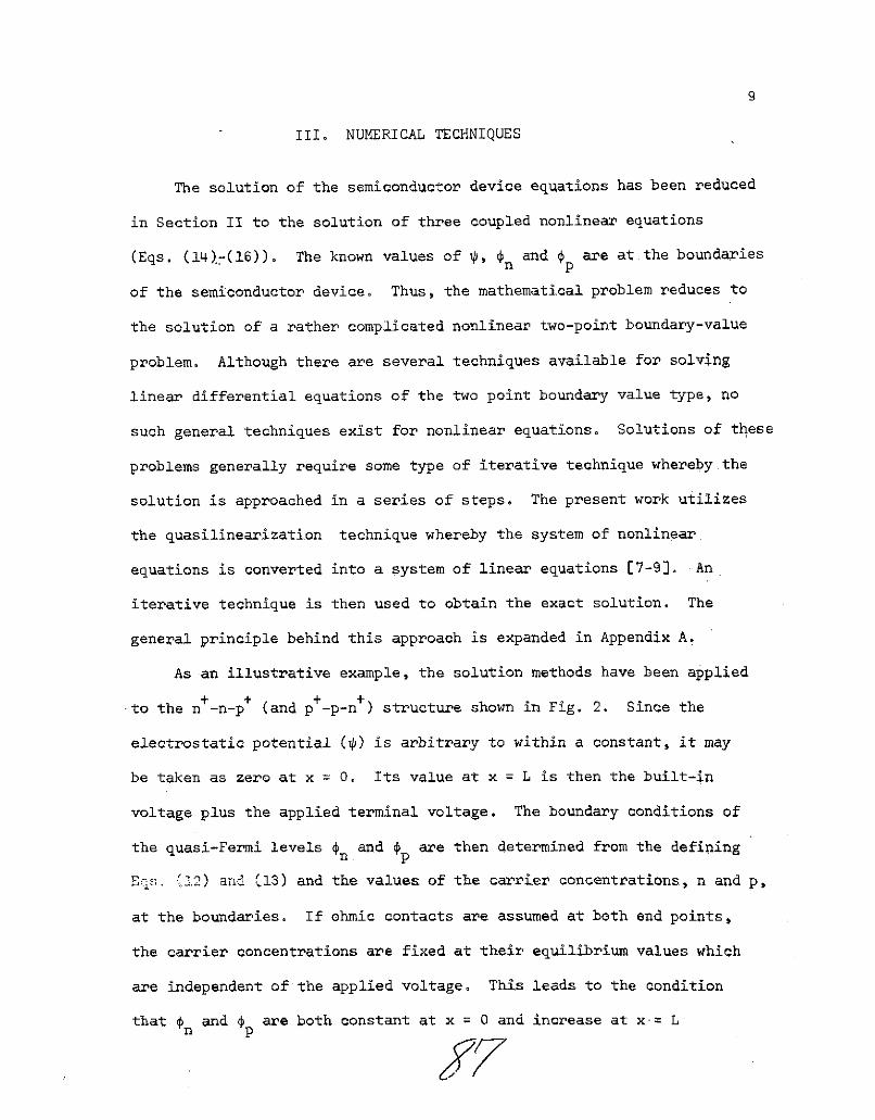
III. NUMERICAL TECHNIQUES
The solution of the semiconductor device equations has been reduced
in Section II to the solution of three coupled nonlinear equations
(Eqs. (14)-(16)). The known values of , n and 4p are at.the boundaries
of the semiconductor device. Thus, the mathematical problem reduces to
the solution of a rather complicated nonlinear two-point boundary-value
problem. Although there are several techniques available for solving
linear differential equations of the two point boundary value type, no
such general techniques exist for nonlinear equations. Solutions of these
problems generally require some type of iterative technique whereby.the
solution is approached in a series of steps. The present work utilizes
the quasilinearization technique whereby the system of nonlinear
equations is converted into a system of linear equations [7-9]. An
iterative technique is then used to obtain the exact solution. The
general principle behind this approach is expanded in Appendix A.
As an illustrative example, the solution methods have been applied
to the n -n-p (and p +-p-n + ) structure shown in Fig. 2. Since the
electrostatic potential (*) is arbitrary to within a constant, it may
be taken as zero at x = 0. Its value at x = L is then the built-in
voltage plus the applied terminal voltage. The boundary conditions of
the quasi-Fermi levels n and $p are then determined from the defining
Ec-. (12) and C13) and the values of the carrier concentrations, n and p,
at the boundaries. If ohmic contacts are assumed at both end points,
the carrier concentrations are fixed at their equilibrium values which
are independent of the applied voltage. This leads to the condition
that n and p are both constant at x = 0 and increase at x.= L

10
directly with the applied terminal voltage. The restriction of ohmiq
contacts at x = 0 and x = L may be loosened to allow for a finite
surface recombination velocity at this end point. However, to more
clearly illustrate the analysis technique, ohmic contacts will be
assumed.
To proceed with the technique, the coupled device equations can be
written in the following functional form:
S ,, a2 n(x,t)
at at n(xt) - 2 n p n(22)
axa8 2 (x,t)
[ - 4]tYp ( x t ) x 2 3 ' n' p' ' p). (23)
The functions Fl, F2 , and F3 correspond to the right hand sides of
Eqs. (14), (15), and (16) respectively.
In the quasilinearization technique (as discussed in Appendix A)
the nonlinear differential equations, instead of being solved directly,
are solved recursively by a series -of linear differential equations.
The linear equations to be solved are obtained from the first order
terms of a Taylor's series expansion of the nonlinear part of the
original differential equation (terms F1, F2 , and F3 above). This
technique is a generalized Newton-Raphson formula.for functional
equations [7-91. In order to illustrate the quasilinearization technique
as applied to the semiconductor device equations, Eq. (22) is considered
as a typical equation.
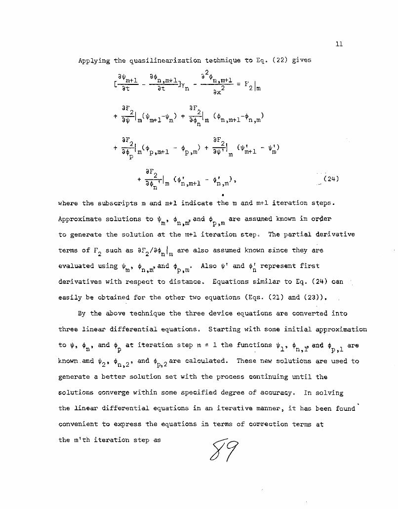
Applying the quasilinearization technique to Eq. (22) gives
Sm+l n2m+l n,m+lS - 2 F2at t n 2 2m
+ 3F ( m - ) + -m -3 m m+1 m n m n,mtl nm
F2 2
+ I I (4' - 4' ) (24)+ I(m On,m+l n,m ) '
where the subscripts m and m+l indicate the m and m+l iteration steps.
Approximate solutions to m' n,9 and 0p,m are assumed known in order
to generate the solution at the m+l iteration step. The partial derivative
terms of F2 such as 8F2/a n m are also assumed known since they are
evaluated using ,m' n,,and 4pm. Also p' and 4' represent first
derivatives with respect to distance. Equations similar to Eq. (24) can
easily be obtained for the other two equations (Eqs. (21) and (23)),
By the above technique the three device equations are converted into
three linear differential equations. Starting with some initial approximation
to *p, n , and 0p at iteration step m = 1 the functions , n , and 4pl are
known and 2' On,2' and Op,2 are calculated. These new solutions are used to
generate a better solution set with the process continuing until the
solutions converge within some specified degree of accuracy. In solving
the linear differential equations in an iterative manner, it has been found
convenient to express the equations in terms of correction terms at
the m'th iteration step as

12
6m = m+l m-
6 n,m n,m+l nm, (25)
6¢p,m p,m+l p,m"
Since the solution is numerical, discrete points in space and time must
be used at which the values of p, 4n, and 4p are calculated. These
points are identified as i,k; where i is an integer specifying the
x-coordinate and k is an integer specifying the time coordinate. Applying
these definitions to Eq. (24), it may be rewritten as
Im,i,k m,i,k m,i,k ax2 m,i,k F21m,i,k
n 2 n F 2
- Y = +
n t I nt 2. 6+ m,i,km1k mntl k ax m,i,k m,i,knm,i,k m,i,k P (
(26)
nmik m,i,k 3 p m,i,k m,i,k
8F2 8F2\t6p' + 6) n-m,i,k m,i,k n m,i,k m,i,k
Similar differential equations may be obtained for 6V and64 p. The
solution to these equations give the corrections to 9, 4n and p at each
iteration step.
The system of differential equations has been solved by the finite
differenceapproach using approximations of the Crank-Nicolson type [10]
for the time dependent case and of the three point difference type for
the time independent case. Following the use of finite differences to

13
approximate the derivatives, a set of three coupled finite difference
equations results, which are of the form,
i i i iA6 1 6. A+ A2 6 + A 6s + A + B 1 6 (27)
i- 11 12 n 13 14 11 i+1
i i i 2
= A2 1 6i . + A22 6 i+ A A +n. 21 i 22 n. 23 p_ 24
(28)i i
B 6i+ + B 621 +1 22 n +
and
i i i iS A31 6i A32 6n. + A33 A34
(29)
i iB 6i+ B 631 it1 + B33 p i+l
The m and k subscripts indicating the iteration step and the time step
have been omitted for clarity since it is understood that the correction
terms are being evaluated for the same time and iteration step. The
i iAjk and Bjk coefficients are complex functions of position and of the
potentials ( , n, and p ) at previous time steps and previous iteration
steps. The above equations relate the corrections to , n, and p at
spatial point i to the corrections at spatial points i-l and i+l. The
A and B coefficients are slightly different for the time dependent and
time independent cases. Exact expressions for the time independent case
are given in Appendix B. Expressions have also been derived for the
time dependent.case [11].
The application of the above equations to a p-n junction is straight-
forward in principle. However, there are several difficulties which must

14
be overcome before solutions which converge can be obtained. One of the
most important of these problems concerns the selection of spatial points
at which 4, n, and 4p are calculated. In a p-n junction at low forward
bias, most of the changes in 4, On and 4p occur over very small distances,
either within the depletion region or for small distances on either side
of the depletion region. To achieve accuracy in the numerical calculations,
any changes in 4, n, or 4p from one spatial point to another spatial point
must be small. This requires that very small steps be employed within
space charge regions. On the other hand outside these regions the quantities
change much less rapidly and efficient utilization of computer time requires
that much larger step sizes be employed. It is necessary then to use a very
nonuniform spatial step distribution. Because of this difficulty Fulkerson
and Nussbaum [5] in their numerical calculations on a p-n junction divided
the device into three regions and used the Debye length as a spatial
normalization constant within the depletion region and the diffusion length
as a spatial normalization constant outside the depletion region. The
approach used in the present work has been to use the same normalized
equations throughout, but to generate a nonuniform spatial step distribution.
The generated spatial step size distribution is such that small
step sizes are taken within regions of space where 4, n, or p are
changing rapidly and larger step sizes are taken when these functions
change slowly with position. This step size selection process is similar
to that developed by De Mari [2]. Since some of the final results (i.e.
J and J ) depend upon an integration of the exponential functions of
4, n', and .p, the criteria on step size is selected so as to maintain a
constant relative error within similar numerical integrations. The
relative error is defined as the fractional difference between a
15
trapezoidal and a parabolic numerical integration of exponential functions
of these variables, and can be set to some convenient value. This in turn
can be related to the step size through the radius of curvature of.the
exponential function [2,11]. At the initialization of an analysis, first
order approximations are used for *, 0n, and p within space charge regions
while final data at a prior voltage increment is used in subsequent voltage
steps. This allows the step selection to adjust automatically to the
changing situation as the applied voltage is incremented. The step
selection has been found to be one of the crucial factors in obtaining
proper convergence. This becomes particularly apparent in very shallow
diffused devices such as.solar cells, since the potentials vary through
a considerable range within very narrow regions. On the other hand there
are basic computer limitations due to round off errors on the minimum
size of a step. Thus a proper balance of step size and number of steps
in a particular region must be maintained. For a typical device run,
calculations can be normally made with 1000±15 steps across a device,
with the normalized step sizes ranging from around 10-1 near the center
of the device to around 10-1 5 near a surface of a shallow diffusion,
Double precision is also used in the calculations to extend the range
of allowed step sizes.
The coupled difference equations for i, #n and p are tridiagonal
matrices. A special technique has been developed for solving a
tridiagonal matrix [9,12] and in the present work this technique has
been extended to the solution of coupled tridiagonal matrices [l].
For given boundary conditions on V, n, and p the solution of the
coupled difference equation is a straightforward procedure. In the

16
present work the boundary conditions are 64 = 6n = 6€p = 0 at both
boundaries of the device since the potentials do not change from one
iteration step to the next.
With the aid of the flow diagram in Fig. 3, the general procedure
for the analysis of a p-n junction such as shown in Fig. 2 can be
summarized. First, information on the device structure such as region
widths, doping levels, applied voltage, etc., is used to calculate
first order approximations to the potential and quasi-Fermi levels
throughout the device. For zero applied diode voltage, the quasi-Fermi
levels are constant across the device and the first order approximation
to p is obtained from standard abrupt junction or linear graded junction
theory depending on whether the junction is abrupt or diffused [13].
For applied voltages larger than zero, the first order approximations
are taken as the converged solutions at the previously calculated voltage
point with the voltage increment linearly added to the previously
calculated potentials. The initial approximations are used to develop
a step distribution and to obtain values for the A and B coefficients
formulated in Appendix B. With these coefficients the linear difference
equations are used to calculate corrections to , 'n, and p . These
corrections are applied to the old values of ., pn, and p and the net
result continues in the iteration loop to form the basis for a new
calculation of the A and B coefficients from which more accurate values
of , On , and p are obtained. The process is repeated until the
largest correction on either , 0n, or p is less than some previously
set quantity (usually 10-4 in this work). When the largest correction
at any point approaches zero the solutions satisfy the original semi-
conductor device equations. With *, n, and p known, the carrier and
current densities can be evaluated.

17
The solution for any number of voltage values can be obtained in a
single computer run. The number of iterations required at each voltage
step is around five when the voltage is stepped in increments of 0.05
volts. A complete forward I-V characteristic can be obtained from
0.0 volts to 0.7 volts in .05 volt increments in about three minutes
of total computer time on an IBM 360 computer. Successful runs have
been made up to 2 volts applied forward bias; however, the major
interest of the present work has been at voltages up to 0.7 volts.
A flow diagram for the time dependent calculations is shown in
Fig. 4. The calculations for this case are carried out in a similar
manner except that each calculation is for a different point in time.
The time increments in the program are similar to the voltage increments
in the time independent analysis program. Most of the work has been
with the time independent program; however, sufficient calculations
have been made to verify that the techniques can be successfully applied
to time dependent problems.

IV. EXAMPLES OF COMPUTED RESULTS
The methods outlined in the previous sections have been applied to
a wide range of abrupt junction n -n-p structures with various doping
densities and region widths. Some of the calculated results have been
previously reported [14]. As illustrations of the results obtainable
from the program, one series of those reported results will be reviewed
and more recent work involving p -p-n shallow diffused devices will
be presented. These were selected in order to illustrate the versatility
of these numerical methods over a rather wide range of diode structures.
Calculated data for two types of devices is included in this work.
+ +These are, first, an n -n-p diode with a lightly doped n region and
wide n and p+ regions. In this device the impurity doping (N(x)) is
assumed to abruptly change values at the junction interfaces. Other
+ +pertinent data on the device is shown in Table III. For this n -n-p
device the center n region is about a minority carrier diffusion length
in width while the n and p regions are considerably wider than a
diffusion length. Calculated plots of potential and quasi-Fermi levels
are shown in Figs. 5 and 6. The rapid changes in potential at the
junction interfaces can be seen in Fig. 5, where the potential change
appears as a step in the curves. Due to the scale of presentation the
space charge regions appear as steps in the figures even though each
region has a substantial number of computational points which can be
retrieved via a numerical printout. Although the high injection region
was reached as evidenced.by the rise in majority concentration of the
n type region seen in Fig. 7, the high bias condition was mostly
dominated by series resistance as seen from the linear
I/

19
increase of potential within the center region at 0.8 volt bias (Fig. 5).
The carrier density curves shown in Fig. 7 are essentially as one would
expect from diffusion model calculations. Details of the changes ip
carrier densities within the space charge regions can again not be
seen due to the scale of representation, so this region corresponds to
the essentially vertical steps in the carrier densities seen in the
figure. The electron and hole quasi-Fermi levels as shown in Fig. 6 are
essentially as one would expect from first order device models. As shown
in the figure, the quasi-Fermi levels are essentially constant within the
depletion region.
+ +The calculated results for a shallow diffused p -p-n device are
illustrated in Figs. 8-12. The analysis of this device has been under-
taken as part of a study of silicon solar cells which is presently in
progress [15]. The dimensions and doping densities correspond closely
to typical solar cell structures. This device has been studied both
without and with optical generation of electron-hole pairs. The potential
and quasi-Fermi level plots at various voltage levels for this device are
shown in Figs. 8 and 10. Again the changes at the junction interfaces
are very abrupt on these scales and appear essentially as vertical lines.
The n region is so narrow that no detail of this region can be seen in
either Fig. 8 or 10. An expanded view of the potential variations with
applied voltage around the p-n junction is shown in Fig. 9. Below high
injection in the center region, which occurs at around 0.6 volt, essentially
all of the potential change with increased voltage occurs across the
+p-n junction. For voltages above 0.6 volts approximately half of the
increments in terminal voltage appear across the p -p junction, as
predicted by first order models of diode behavior.

2Q
Electron and hole densities are shown in Fig. 11 for the entire
device, and an expanded view at the p-n+ junction is shown in Fig. 12.
The boundary condition of an ohmic.contact at the surface forces the
surface values of p to be independent of applied bias. Expanded views
are quite necessary in this device to see any variation of n and p at
the p-n junction interface.
This same device was analyzed with the inclusion of a generation
rate due to solar irradiance. Fig. 13 illustrates the overall change
in the carrier distributions and Fig. 14 expands this data about the
+n -p junction near the irradiated surface. These figures can be
compared directly with Figs. 11 and 12. The inclusion of a generation
term represents a rather heavy perturbation of the program but it was
found quite easy to add the generation rate in steps to an already
convergent solution at some high forward bias. After stepping in
powers of 2 from Ge/128 to Ge/l at the same forward bias, the voltage
could then be incremented downward in the same fashion as before in
order to obtain a full characteristic. Once the program converged with
the full generation term, it incremented in voltage to the short circuit
condition without any difficulty.
Although no results are shown in this paper, the programs also
evaluate the terminal current density at a given voltage, and generates
terminal I-V characteristics. The evaluation of current density is
straightforward from the device equations after 9, #n and p are known.

21
V. SUMMARY
The technique of quasilinearization and the numerical techniques
discussed herein have been found to be a very good approach to
semiconductor device analysis. The techniques have been found to lead
to rapidly converging solutions under a wide variety of physical
conditions. These cover the range of devices which are narrow compared
to the minority carrier diffusion length to devices which are very
wide compared to the minority carrier diffusion length. The approach is
also able to very easily handle high injection effects in p-n junctions,
high-low junctions, and optical generation. The exact analysis is
providing very useful information on the operation of solar cells.
With the analysis program a much more complete understanding is possible
of solar cell operation and especially of the interactions between p-P
junctions and high-low junctions in solar cell structures [15].
The results reported herein are but a small sample of the computed
results which have been obtained on semiconductor devices. The included
results illustrate the application of the program to two physically
very different diode structures. The analysis program is able to analyze
both types of devices with only minor changes in input parameters.

22
VI.- ACKNOWLEDGEMENTS
The authors would like to acknowledge the partial support of this
work by.the National Science Foundation through NSF Grant GK-13752 and
the National Aeronautics and Space Administration through NASA grant
NGR 34-002-195.

23
Table 1 Normalization table
Normalized Description NormalizationQuantityDescription Factor
x position coordinate LD (=/eVt/qni )
t time coordinate L /Do
r T lifetimes LI/Dono pDo
electrostatic potential Vt (= kT/q)
n' p quasi-Fermi levels Vt
VA applied (or terminal) voltage Vt
E electric field V t/LD
n,p carrier densities n
N, ND, NA net impurity, donor, and acceptor n.densities
J, J, J total, electron, and hole current -qDoni/L DSP densities
D , D carrier diffusion constants D (= 1 cm 2/sec)n p o
Pn' Pp carrier mobilities D /V
U generation-recombination rate D n./L
G external generation rate Doni/L.
e o D

24
Table II. Constants for mobility expressions (normalized values)
C1 81 K1 350
C 2o6x10 8 K2 7.0x1082 2
C3 1.76x10⁻⁶ K3 1,93xl0 - 6
C 70xlO4 K. 176x104
C 1.25xl0 K5 1,18xl04
-1 -1Un 34.93 p1 12.42no po

25
Table III. Data on two diode types studied
+ + + +n -n-p p -p-nDevice Device (Solar Cell)
+ 18 3 + 18 3n doping 10 18/cm3 p doping 180 /cm3
15 3 15 3n doping 2.5xl015/cm p doping 1.3xl0. /cm
+ 18 3 + 20 3p doping 10 /cm n doping* 10 /cm
+ +n width 250 um p width 0.5 Pm
n width 100 Um p width 249,25 ~m
p width 250 um n width 0.25 pm
-7 -7t 10 sec T 10 secpo po
S10 - sec T 10 secno no
*n+ region is a Gaussian diffused region. The value of doping density isthe density at the surface.
26
APPENDIX A
The quasilinearization or Newton-Raphson approach to nonlinear
problems was first introduced by Bellman [9], extended by Kalaba [10]
and applied to many engineering problems by Lee [11] To illustrate
the mechanics of the technique, consider the equation
L[X(t)] = g(X,t) (A-l)
where L is a linear operator (partial or ordinary) operating on the
desired function X(t) and g is some nonlinear function of X. Performing
a Taylor series expansion of the nonlinear function about a given
initial estimate Xo(t), one obtains
L[X(t)] = g(Xo ,t) + (X-X ) g'(Xo,t) + ----- (A-2)
where the prime indicates differentiation with respect to X. Neglecting
second.and higher order terms of the expansion, Eq. (A-2) becomes
LEX(t)] = g(Xo,t) + (X-Xo ) g'(X 0t), (A-3)
which is a linear equation which can be solved for X(t) = X (t). Using
this result to formulate
L[X2 (t)] = g(Xl,t) + (X 2 -X1 ) g'(X1 ,t), (A-4)
the iterative process can be continued until the desired solution X(t)
is obtained. Of course, this procedure assumes convergence of the
sequence of functions X m}. Although at first this seems to be a rather
severe restriction, for many of the commonly occurring linear operators,
the sequence does indeed converge. In fact, for all functions attempted
by the authors, convergence was accomplished. It should also be noted
that if convergence does occur, then this convergence is quadratic in
nature [9,11]. That is, as convergence is approached, the maximum error
27
(or correction) in a given iteration is proportional to the square of
the maximum error of the previous iteration.
In summary, the quasilinearization technique is essentially a
Taylor Series expansion (in function space) of the nonlinear portion
about each of the individual functions making up the nonlinearity.
The resulting linear equation is then solved in an iterative fashion
subject to the boundary conditions imposed by physical considerations.
As evidenced by the equations in the body of this paper, the
quasilinearization technique is applicable to multi-dimensional and
multi-functional nonlinear equations.

28
APPENDIX B
Expressions for the A and B Coefficients for the Time Independent Case.
a. s i-
A = [s- + (s+s ) ], (B-3)1 a i 2 -i-l a -
S s (s1 + (F+s , (B-2)12 2 i i-l 1 i
1
1i 2-1 (s.+s.) , (B-3)
i 5i-1A = [- (s.+s. _)(F - '). (B-4)
14 2 1 1-1 1
i = i/ (B-5)
s. s+s F i DF2 Fi 1 -A)
1 F {1 ag 2 11 '221 2 1 aA2+s. - i i i
(B-6)
s. s.+si1 8F2 2(ei+1)22 { i n s.ii
2 ~ - A12 J-'- (B-7)2 ' 12i n
1

29
si(si+si ) DF2 so 8F I F2Ai 1 1-1 1 } (B-8)A23 F2 -p 2 (B-8)
2 + s. 2 p p
si(s+s i F21
n i
A s(sis. 1 ) It s. 8F2
S= F2 1 ] , (B-109)
2 + s i
21 i-i i - l
n .
1
1 aF 2 CF2
B2 = Es. (1) .] / [2 + s ], (B-I)
22 i-1 a. DO' si n
s. si+si F31
2+ s i li 2
22 -i S 2F3± 1 (B-i)n . n.
1 1
2 11 3
A I si-i i+l31 3 a1 i
2 + s. 2
2(- 3 -A -i; 1 (B-12)
2 s. 13
P .
I

S i- (S i+Sil ) S. DF 3
A tF--1 F I 3034 13 p i 22 + s i 3 7 i
.(B-15)
i [si 1 ai+l) F3 [2 + s'F3
i S 3 2
S= [ i- 1 3 2] f (B-17)Tal 1 P33 1F
3 1 p 12+ s. ol
In the above equations si is the magnitude of the step in going from
x. to x. and a. is the ratio of si to Silo Expressions for the
various partial derivatives of Fl, F2 , and F3 are given in the following
tables:
Table B.1 Partial derivatives of F1
FI(', , n' p) = exp[P-¢n] - exp[ p-] - N(x)
F 1 1= exp[-1n] + exp[Cp-IJ
aF- = -exp[T- n
n
.1 -exp[ - 3
p
62SY

31
Table B.2 Partial derivatives of F2
d4n 1 dyn ddF2( p n 1 yn _ n d -- + Yn(x)Ge(X)exp(n-2 n '~p n dx 'y dx dx dx n e n
exp[ -*] - exp[4 -i]
n+ y(x)Tp l+exp(- n)]+T noCl+exp(P -)]P0 n no P
(T +T )[exp(4 -i) - exp(4 -)] + 2 poexp( p- n)-l]8F2 no po p n pP
-= X) {t [il+exp(-n)] + Tno [1+exp( p - ) ] } 2
-y (x)Ge(x)exp( n-)
(T + T )exp(n-) + Tno exp( n+p-2) + T po2-exp( p-n )]F no po nopn
-=n ( x )n T po[l+exp(-yn)] + Tno l+exp(p -)]} 2
po n no p
+yn(x)Ge(x)exp( n-0
(x +T )exp( -p) + T 0 exp(- ) + T exp( 2)
S-yn(x)p n Tpoll+exp(-¢n + TnoEl+exp( p- )]} 2
9F2 d n(x)
Ba' dx
F 1 dn(x) d(X) (x) (x)+2 d(x)
yn dx dx dx
627

32
Table B.3 Partial derivatives of F3
dy d4 d9F ( p,4 d dxL - (x)G (x)exp(-0 )
exp(- cn) - exp(-qp )
p( po Ll+exp( - n) ] no[l+exp(p -)]
(T +T )[exp(p-4 n) - exp(*- p)] + 2T no[exp( p-n)-]yF3 no po n p no p
{T po [lexp(- n)] + T no[+exp( p- )]}2
-yp (x)e (x)exp( -p )
F 3 (Trio + po)exp(- n) + T exp(4 p-n) + Tpoexp(2- n-0 )
- = -(X)S-n IT po [l+exp(4-On)] + T nol+exp(4 -ip)]}2
DF 3 (Xno + po )exp(-4 ) + T poexp(2p-O n-p ) + no[2-exp(4 -n )]--- : yp (X)p {IT po[l+exp(4- n) + T nol+exp(4 p- ) ]}2
+yp (x)Ge(X)exp(-p )
F3 . d# (x)
41' dx
aF dy (x) d (x)(x)F -+ 2d -
p y y dx dx
P62

33
REFERENCES
1. H. K. Gummel, IEEE Trans. on ED, ED-11, 455 (1964).
2. A. De Mari, Ph.D. Thesis, California Institute of Technology (1967).
3. C. M. Lee, R. J. Lomax, and G. I. Haddad, IEEE Trans.on MTT, MTT-22
160 (1974).
4. M. S. Mock, Solid-State Electronics, 15, 1 (1972).
5. D. E. Fulkerson and A. Naussbaum, Solid State Electronics, 9,
709-719 (1966).
6. C. W. Gwyn, D. L. Scharfetter, and J. L. Wirth, IEEE Trans. on NS,NS-14, 153 (1967).
7. R. E. Bellman, Proc. Natn. Acad. Sci. U.S.A., 41, 743 (1955).
8. R. Kalaba, J. Math. Mech., 8, 519 (1959).
9. E. S. Lee, "Quasilinearization and Invarient Imbedding",
Academic Press, New York (1968).
10. J. Crank and P. Nicolson, Proceedings of the Cambridge PhilosophicalSociety, 43 (1), 50 (1947).
11. E. D. Graham, Ph.D. Thesis, N. C. State University, Raleigh, N. C.,
(1970).
12. G. H. Bruce, D. W. Peaceman, H. H. Rochford and J. D. Rice, Trans. AIME198, 79 (1953).
13. S. M. Sze, "Physics of Semiconductor Devices", Wiley, 1969.
14. E. D. Graham and J. R. Hauser, Solid State Electronics, 15, 303-310(1972).
15. Complete details of this work will be published elsewhere.

34
FIGURE CAPTIONS
Figure 1i. Spatial dependence of electron-hole pair generation rate for
full spectrum (AMO) irradiance on silicon.
Figure 2. The basic n -n-p (or p -p-n ) diode structure.
Figure 3. Flow diagram of semiconductor device analysis program
(Time independent case).
Figure 4. Flow diagram of semiconductor device analysis program(Time dependent case).
+ +Figure 5. Electrostatic potential variation in n -n-p device.
Figure 6. Quasi-Fermi potential variation in n -n-p device
(measured above equilibrium value of -0.466v).
Figure 7. Hole and electron density variation in n -n-p device.
+ +Figure 8. Electrostatic potential variation in p -p-n device.
Figure 9. Electrostatic potential variation about n -p junction.
+ +Figure 10. Quasi-Fermi potential variation in p -p-n device (measured
below equilibrium value of 0.466v).
Figure 11. Hole and electron density variation in p -p-n device.
Figure 12. Hole and electron density variation about n -p junction.+ +
Figure 13. Hole and electron density variation in p -p-n device
under full spectral irradiance (Irradiated surface at
x = 250 microns).
Figure 14. Hole and electron concentration about n -p junction nearirradiated surface.
//0

1021
I-'
1070
C-)N. 1021L.
10 '1017
10 10 10 100 10' 102 10
DEPTH -( M)
Figure 1. Spatial dependence of electron-hole pair generation rate forfull spectrum (AMO) frradiance on silicon.

Incident Light
(if present)
n n pp V
(p) (p) (n) a
X=0 X=MI- X=M2 X=L
++ or p-p+ diode structure.Figure 2. The basic n -n-p (or p -p-n ) diode structure.

S READ DEVICE READ APPLIED CALCULATESTART STRUCTURE VOLTAGE FIRST ORDER
PARAMETERS I DEVICE PARAMETERS
CALCULATE TRIAL POTENTIAL CALCULATE STEP
AND TRIAL QUASI-FERMI -. SIZE ACROSSLEVELS DEVICE
CALCULATE OPTICAL CALCULATE MOBILITY CALCULATE
CARRIER -- I FROM DOPING H QUASILINEARIZATIONGENERATION & ELECTRICFIELD COEFFICIENTS (A,B)
NONLINEAR EQUATION ITERATIVE LOOP
CALCULATE CALCULATE CORRECTIONS
CORRECTED - TO. P, , n' p AT EACH
1' n' p POINT ALONG DEVICE
CALCULATE CARRIERNO ACCURYES DENSITIES, CURRENT
IINT DENSITIES, TOTALCURRENT AND EFFICIENCY
PRINTING AND PLOTTINGOF RESULTS
YES 0YES REPEAT NO END
figure 3. Flow diagram of semiconductor device analysis program(Time indepnden't case).

CALCULATION OF I APPLIED
FIRST ORDER VOLTAGE
QUANTITIES DATA
CALCULATE CALCULATE APPLIED VOLTAGE,ETERMINATION OPTICAL TRIAL POTENTIAL AND QUASI
OF TIME CARRIER FERMI LEVELS AT NEXT
STEP SIZE ENERATION TIME POINT
COMPUTE MOBILITY FROMDOPING AND LOCALELECTRIC FIELD
QUASILINEARIZATIONSCHEME, SOLUTION
AND CORRECTIONS TO
, On , and 0p
ACCURACY NOSUFFICIENT
YES CALCULATION OF CARRIERCURRENTS AND CARRIER
DENSITIES
LAST PRINTING AND PLOTTINGTIME : ' - OF RESULTS
NO POINT
YESEND
Figure 4. Flow diagram of semiconductor device analysis program(Time dependent case).
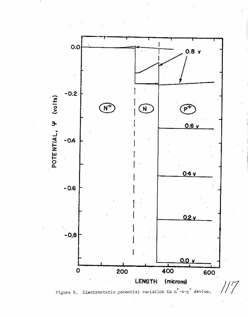
0.00.8 v
-0.2
-0.6 y
a.
1-
0.4 v
-0.6
-0.80,8
0.0 1 -
0 200 400 600LENGTH (microns)
Figure 5. Electrostatic potential variation in n -n-p device.

0I I
> I
0'0.6 0.6 v ,I-
S- I / "
cft
w II0.4 v/
I/ I
n+n
. Il / /
II
0
0 200 400 600
LENGTH (microns)+ +
Figure 6. Quasi-Fermi. potential variation in n -n-p device (measured
above equilibrium value of -0.466v).

.OII
z oIs - - n ----
'10
1020. v \ \ \.7v
cc 0.4 \0,4 vS10 O. .
(0-x Ov
S0.2v I \0.2v \\ \% \
0 200 400 600
LENGTH (microns)+ +
Figure 7. Hole and electron density variation in n -n-p device.
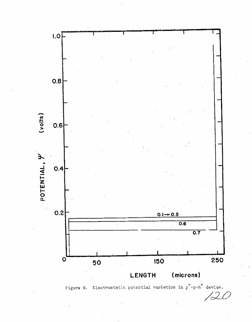
1.0 I I I
0.8-
o 0.6-
,- 0.4-
z
0
--
0.2b 0.1 o. 5
0.6
0.7
0 50 150 250
LENGTH (microns)
Figure 8. Electrostatic potential variation in p -p-n device.

, ," I .. ' I .. . I I I -
1.0
.OI
o
0.6
0.J
S0.4I-zW0.
0.
0.2
S0.7 v
0 0.5 1.0 1.5
LENGTH (microns)
Figure 9. Electrostatic potential variation about n -p junction.

0.6
S -0.1 --- O
l - --CS-0.2 -- .........--.- --.... ---..----- -
<0.3--.4 o.3 -
0 -0.40
J-0.U. 0.5
-0.5
CO+
ah ,,, 0.6
-0.6
0 50 150 50
LENGTH (microns)
Figure 10. Quasi-Fermi potential variation in p -p-n device (measuredbelow equilibrium value of 0,466v).

L0
I 0.7
i 0.5
u)
- 0.4
LU
a 1 0.310
0.1
I p -
. I I I
0 50 150 250
LENGTH (microns)
Figure 11. Hole and electron density variation in p -p-n device.
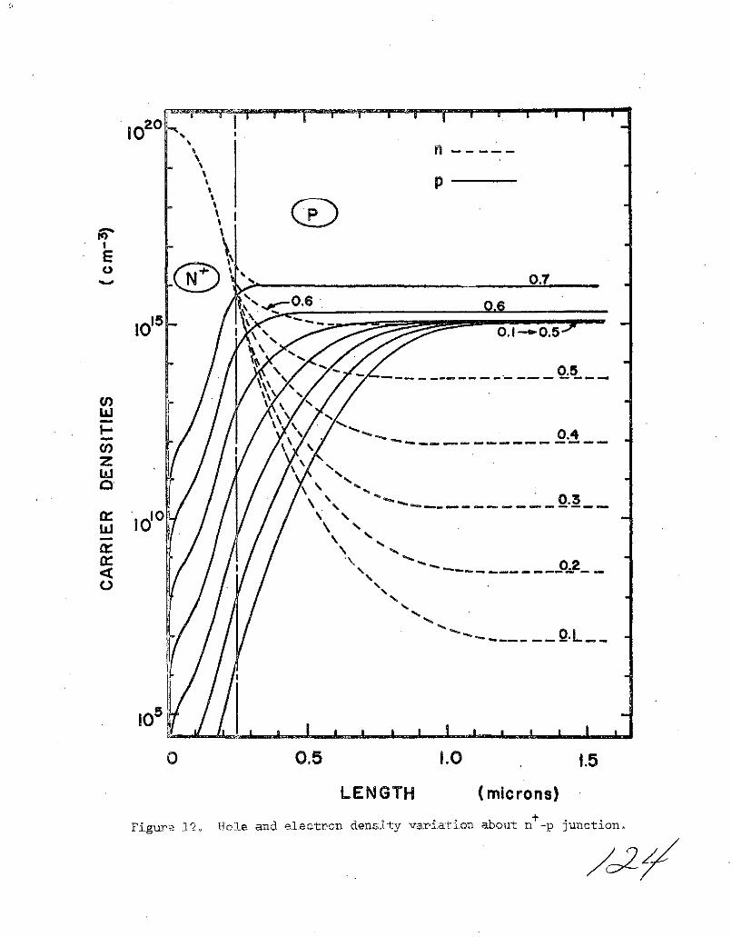
20 110
0 -----' 1
Eto
'' 0.7
0-0.6 0,6
,15
w. -0.4
\0. 0.3
<, .0.2
10
0 0.5 1.0 1.5
LENGTH (microns)
Figure J.2, Hole and electron density variation about n -p junction.

10 0.6
CO
E 0O 50 o-0 -50
z
a
10
0 50 150 250LENGTH (microns)
b- -- -------
Figure 130 HFle r, d e-le:ra densty varia ,n in p -p-n device under: ;rria-Mar! (I a.adated surfae a,- x 250 microns).

\P
\10
z
0 \
\ P ------
.0. v
N p
10
I
0 0.5 1.0 1.5
LENGTH (microns)
Figure 24, Hole and electron concentration about n -p junction neari-?a>ted surface,

Appendix B: Optical Carrier Generation in Silicon
P. M. Dunbar and J. R. HauserElectrical Engineering Department
North Carolina State University, Raleigh, N. C. 27607
ABSTRACT
A numerical analysis of the spatial dependence of optical
generation of electron-hole pairs in silicon due to full solar
spectral irradiance is reported. The analysis includes the
utilization of published experimental data on solar spectral
irradiance, index of refraction, and absorption coefficients. Of
particular interest is the illustration of the depth to which one
must collect optical carriers in order to utilize given amounts of
the incident photons. A determination of reflection and transmission
coefficients is made for various thicknesses of SiO and Si02
antireflection coatings and optimum thicknesses for photon
transmission are reported. Absorption in the SiO layer is included.

I. GENERAL FINDINGS
Electron hole-pairs generated in a semiconductor arise from the
interaction of photons with the valence band electrons in the semicon-
ductor. The irradiated material is characterized by the absorption
coefficient, a, which is a rather complex function of the incident
photon energy. For full solar spectral irradiance, the number of
incident photons as well as the reflectance properties of silicon are
quite complex functions of the photon energy. Also at the higher
energies of the solar spectrum the internal quantum efficiency exceeds
unity. For these reasons an analytical development of the optical
generation rate due to full spectral irradiance has not to date been
undertaken. The present work incorporates experimental or empirical
data concerning each of the above parameters in order to formulate the
spatial dependence of the optical generation .rate. This is performed
for both air mass one (AMl) and air mass zero (AMO) solar spectral
irradiance. Also calculated are the effects of both SiO and Si02
antireflection coatings on generation rate and the optimum thickness of
these layers for maximum photon transmission into the silicon substrate.
Absorption in the SiO film is included. Prior work in this area. has
been limited to equal energy spectral response and does not integrate
into the response the full spectrum of solar irradiance, reflection
losses, quantum efficiencies, or absorption in the antireflection
film [1-81.
For monochromatic radiation an incident wave will decay in energy
exponentially with respect to distance. This can be expressed as:

2
P(x) = P(O) e-x (1)
where a = fC is the absorption coefficient, and kc, the extinction
coefficient, is the imaginary part of the index of refraction.
Neglecting internal reflections the maximum current resulting from
this incident energy may be expressed as:
JGe = ffqT(X) Nphi(X) n l-exp(-a(X)x)] dA dx, (2)
where T is the transmission coefficient, Nphi(A) is the incident
photon density per wavelength interval, and qX is the internal quantum
efficiency. The generation rate is also expressed as
Ge(x,X) = T(X) Nphi(M) nI c(A) exp(-a(A)x). (3)
A detailed discussion of the methods used to model the various components
in the above expression is given in the next section. Figure 1 however,
illustrates the resulting spatial variation of the calculated generation
rate for a bare Silicon surface. Shown in Fig. 2 is the effect of
SiO and SiO 2 single layer anti-reflection coatings under AMO conditions.
For AMO conditions the generation rate is seen to exceed 1022/cm3.sec at.
the surface and to decrease rapidly with distance into the semiconductor.
A significant decrease is seen in generation rate as close as 10-6cm (10-2 m)
from the surface.
A graphic illustration of the very rapid decay of the generation term
can.be obtained through an integration of the generation term versus
distance. This calculation yields the maximum optical generation
current as a function of the device depth over which optical carriers
are collected. The result is presented in Fig. 3 in terms of the
collection efficiency as a function of device thickness.
/ C

3
It is assumed in this calculation, as in the others, that the back contact
is transparent. The total optical current in this work is defined as the
total photon current which is present in the visible spectrum above the
silicon band edge (1.11 eV in this work). The results for the other
geometries and AM1 irradiance are within 2 or 3 per cent of this curve.
Table 1 summarizes the various optical parameters used in the
calculations and results obtained. The total surface loss for a.particular
condition is the percentage of incident photons which are not transmitted
into the device. This loss includes reflection and any absorption in the
antireflection layer. Since the reflecting nature of.silicon and any
antireflection layer is strongly dependent of incident wavelengths the
total surface loss will vary from AM1 to AMO due to the difference in the
two spectral densities. Results similar to these were presented by
Milnes and Feucht [9]; however, their work assumed the Si0 layer to be
fully transparent, while in this work losses in the SiO layer have been
taken into account. The theoretical calculations predict an optimum
o oantireflection coating of about 800A for SiO and about 1100A for Si02'
The predicted surface loss for SiO layers is slightly less than that
for Si02
/,30

II. REVIEW OF FACTORS DETERMINING GENERATION RATE
It is known that monochromatic photon absorption has an exponential
dependence upon the absorption coefficient, a. Although it is possible
to determine a functional dependence of the absorption coefficient upon
photon energy it is quite complex, so experimental data on a vs. X
has been used. This data is that of H. R. Phillip [10], and Dash and
Neuman [11]. However, in using this data it is necessary to review
the major absorption processes in order to justify any assumptions
pertaining to quantum efficiency. The single most important process
for solar cell operation is that of intrinsic absorption, which is the
generation of hole-electron pairs by photons of energy.larger than the
band gap energy. This is the most predominant mechanism in the solar
spectrum range of wavelengths.
At energies above about 3/2 the band gap energy.there is the
possibility that hot carriers may create secondary pairs via impact
ionization and thus raise the quantum yield above unity. This becomes
appreciable in silicon for incident energies above 3 ev and is included
in this present work by the following empirical model of Shockley E123:
= 3-2 exp(3.3-h), hv > 3.3 ev (4)
Although this increase in quantum yield is included, it can be considered
somewhat secondary due to the low spectral power above 3.3 ev. Also the
high absorption coefficients in this range of energy imply high surface
absorption and probable subsequent loss due to surface recombination which
would be present.
X51'
5
At energies at and below the absorption edge there are several
mechanisms. The more important of these is free carrier absorption.
This absorption is seen as a rise in a for photon energies near and
below band edge. Of course, this mechanism has a quantum yield of
zero. This zero yield is simulated by omitting any appreciable
absorption coefficient data for energies below the band edge. However,
free carrier absorption does still occur for energies above the band
edge and could conceivably lower the effective quantum efficiency.
Data by Spitzer and Fan [13] indicates a dependence of a on the square
of the wavelength and on the carrier concentration. An extrapolation
of their data to energies above the silicon band edge indicates that-1
a is at most 50 cm-1 . Thus, the typical device will be effectively
transparent to this effect.
Other low energy absorption mechanisms include lattice vibrations,
exciton generation, band tailing, isoelectronic traps, and extrinsic
centers (non ionized impurity centers) [14,15]. However, all of these
are appreciable only into the infrared and even then have extremely
low absorption coefficients. These were neglected in the development.
of the generation term in the same manner described above.
Reflection from the surface of the sample must be taken into
account. A polished silicon surface, calculated as shown below,
will lose in the neighborhood of 35% of the incident photons due to
reflection. With a single layer antireflection coating this loss is
reduced appreciably as shown in Table 1. For the structure illustrated
in Fig. 4 the optical coefficients can be written as:
2-3

r22 + 2r12r23exp(-26)Cos[26-(23 - 12)] + r2 32exp(-4a) (5)
1 + (r12r23) 2exp(-48) + 2r12r23exp(-2$)Cos[26-( 23 + €12 )
(t12t2 3)2 exp(-2a) 6)T =(6)1 + (r 2r23 2exp(-4a) + 2r12r23exp(-28)Cos[26-( 2 3
+ 12
T + R + A = 1, (7)
2 2 2 21/2
1 2 c2 c2nL (n n _ k2 2+ (2kc2n 1 ) 2
12 2 2(nl+n2) + ko2
2 1 / 2
(n 2 n 2 + kc2 _ k 2) + [2(n k nk 2) 1/2
{2 3 c2 c3 2 c3 3 c223 (n2 + n3) +(kc2 + kc3 )
2n11 (10)
12 [(nl+n2)2 + k 2 2 (
1 / 2
2{[n2(n2+n3) + k c(kc2+kc3)l 2+ (n2kc33k2 (11)
23 (n2+n3)2 + (kc2+kc3)
6 2 n2 d, (12)
$ = 27 kd, (13)
-1 2 1c2012= Tan f22 (14)
n 1 2 k c2
€1 Tn 1 2 2 /" 2} / (1 1

7
-a i 2(n k3 - n3k c2S=Tan- 2 2c3 3 c 2 (15)232 - n3 - kc3 + kc2
The quantities r1 2 , r2 3 , t12 , and t2 3 can be viewed as the magnitudes of
the complex Fresnal Coefficients. The phase shifts €12 and ¢23 are due
to absorption in the antireflection layer and the silicon respectively.
In the above formulations "n" is the real part of the index of refraction
and kc is the imaginary part. For a transparent film, kc2 is zero, as is
In performing this calculation with a silicon substrate, experimental
data for a, n3 , and kc3 versus wavelength were utilized. Results yielding
the transmission coefficient as a function of photon energy are shown in
Fig. 5. The reflectance for a bare silicon surface (d = 0) shown in the
figure agrees directly with the data of H. R. Phillip [10]. Also shown is
the transmission coefficient for an antireflection film of Si02 at its
optimum thickness. For StiO, the transmission, reflection, and
absorption coefficients are illustrated in Fig. 6. These optimum thicknesses
are determined by the maximum efficiency of photon transmission into the
substrate as described below.
The results for photon transmission efficiencies for both SiO and
SiO2 are shown in Fig. 7 as functions of antireflection layer thickness.
This illustrates an optimum thickness of around 1100A for SiO2 and
0
800A for SiC. It has been assumed in this calculation that the SiC 2
layer is transparent within the spectral region of interest with a
constant index of refraction of 1.44., This is a good assumption for
Si02, but SiO is somewhat lossey in this region. To include this
absorption, the data of Hass and Salzburg [16] of the index of refraction

and extinction coefficient was used to determine values for n2 and
k c2.for SiO. This data is illustrated in Fig. 8.
The available experimental data on reflectance from silicon surfaces
is somewhat scattered. Prince has reported a maximum reflectance of 6%
in the spectrum below 3 ev [4], while Phillip [101 and Malovetskaya p17]
present data illustrating reflectances ranging over 30% within the same
spectral energies. The reflectances calculated in this report for
bare silicon (Fig. 5) agree closely with the most.recent experimental
data of Phillip. Although the program utilized the index of refraction
and absorption coefficient data calculated by Phillip from the
experimental reflectance measurements, it should be realized, however,
that the absorption coefficient data is essentially the same experimental
data as that published by Dash and Neumann [11]. Although Malovetskaya
does not reportthe thickness of the SiO 2 layer utilized in his work,
he does report a maximum transmission of about 93% at 1.5 eV for this
case. This agrees quite well with the calculations presented in this
paper.

9
III. CALCULATION TECHNIQUES
Utilizing the data and equations discussed in the previous
section a computer program has been developed to calculate the carrier
generation rate under various conditions including that of a general
single layer antireflection coating. The general flow of the program
is illustrated in Fig. 9. The incident photon density is determined
from published data on full spectrum solar irradiance. A most
comprehensive collection of data on solar radiant energy is the
NASA document for Space Vehicle Design Criteria which develops final
data from weighted averages of several investigations [18]. The
parameters of interest are the solar constant and the solar spectral
irradiance. The data used for irradiance under AM1 conditions (sea
level) is that of P. Moon [19]. Due to great uncertainties as to
atmospheric absorption and latitude of measurement this data must be
viewed as typical. The data was read numerically and stored in the
program. The incident photon density is related to the photon energy,
irradiance, and wavelength interval as
H
N (#/sec/cm 2 ) (16)phi E
where (-!) is the average irradiance over an increment of AX, and E
is the average energy of the AX increment. The published data is a
tabular form of ( -H) versus wavelength. All available data above 1.lleVLX
and up to about 7 eV was included.
The next stage in the calculation is to read into the program the
published data for the absorption coefficient and index of refraction

10
for silicon, This data was supplied in tabulated form from H. R. Phillip
[101. These values are interpolated to the wavelengths of the spectral
irradiance data. This then supplies Nphi , a, n 3 , and k for each
wavelength available from the solar spectrum data. With these values
the reflectance of the Si surface and the Si-SiO2 surface can be
calculated. For the SiO layer a similar interpolation process on the
index of refraction (n2) and extinction coefficient (k 2) data [16]
allowed the calculation of these coefficients at the relevant wavelengths.
At this point the surface photon efficiency nN is calculated as
ENphi T qX
N N (17)
E phi
where T is the transmission coefficient. The surface loss of Table 1 is
1-nN .
Prior to calculating the generation rate, a spatial distribution
is developed which limits the change in Ge between spatial points to
about 10%. This then allows the generation rates to be calculated at
each spatial point by summing the contribution to Ge of each incident
wavelength. Once this data is developed in a tabular form, it is
numerically integrated to obtain the spatial dependence of the maximum
optical current.
The total number of incident photons in the visible spectrum for
energies above the silicon band edge (,o11 eV for this work) sum to
3.31 x 10 17/cm2 for AMO and 2.14 x 10¹⁷/cm2 for AM1. These values are
about 5% below what is normally used. There is, however, some ambiguity
as to the proper value of these quantities since the published irradiance
data for AMO and AM1 vary somewhat. Also, since silicon is an indirect
377

band gap material, there is not a sharp edge to the absorption curve making
the assignment of the band gap energy somewhat ambiguous. For the AMO
condition a 3% change in the energy band gap (i.e. from 1.08 eV to 1.11 eV)
can result in a 3% decrease in the total number of incident photons.
Photons at these energies, however, contribute little to the photocurrent
due to the extremely low absorption coefficients in the immediate vicinity
of the band edge. The photon density from the irradiance data corresponds
to an available current of 52.9 mA/cm2 for AMO and 34.2 mA/cm2 for AM1.
The inclusion of enchanced quantum efficiency at higher energies resulted in
a 1.5% increase in the total available current over the total spectral
current for AMO. The increase for AM1 was quite insignificant, being below
0.5%.

12
IV. CONCLUSIONS
It is found that the spatial decay of the optical generation rate
in silicon due to solar irradiance is extremely rapid. This very rapid
decay may allow narrower devices in collection applications than
previously expected; however, it also indicates the importance of
surface treatments to greatly reduce surface recombination. For AMO
applications the SiO and SiO 2 antireflection layers are seen to be
roughly equivalent, with the SiO layer slightly more efficient. This
rough equivalence-points out the need to include the absorption
characteristics of the SiO film, for this degrades the efficiency of
this film by roughly 5%. However, the optimum thickness for the Si0
o 0
layer is somewhat thinner than the SiO 2, 800A vs. 1100A. In the actual
use of SiO as an antireflection layer on solar cells the difference
between SiO and Si02 is likely to be greater than indicated by the
photon efficiency calculation. The SiO film results in a lowered
generation rate near the surface and an enhanced generation rate deep
within the silicon. Thus surface recombination losses may be less
with SiO than with SiO 2 (assuming the same surface recombination
velocity) giving SiO a slightly larger advantage over SiO2 . For AM1
applications the optimum film thicknesses are approximately the same
as AMO. The Si0 film is still somwhat more efficient than the Si02
with the diffrence slighti mor6 pronounc dsInce thb AM1 spectrum
is quite deficient in higher energy photons.

13
ACKNOWLEDGEMENTS
The authors would like to express their gratitude to
Dr. H. R. Phillip for supplying tabulated data of the absorption
coefficient and index of refraction for silicon.

14
REFERENCES
1i. M. B. Prince, J. Appl. Phys. 26, 534 (1955).
2. J. J. Loferski, J. Appl. Phys. 27, 777 (1956).
3. M. Wolf, Proc. IEEE, 48, 1246 (1960).
4. M. B. Prince and M. Wolf, J. Brit. IRE, 18, 583 (1958).
5. J. J. Loferski, Proc. IEEE, 667 (1963).
6. M. Wolf, Energy Conversion, 11, 63 (1971).
7. L. M. Terman, Solid St. Electron, 2, 1 (1961).
8. P. Rappaport, RCA Review, 20, 373 (1959).
9. Milnes and Feucht, Heterojunctions and Metal Semiconductor Junctions,p. 134, Academic Press (1972).
10. H. Phillip, J. Appl. Phys., 43, 2835 (1972).
11. W. C. Dash and R. Newman, Phys. Rev., 99, 1151 (1955).
12. W. Shockley, Solid-St. Electron, 2, 35 (1961).
13. W. Spitzer and H. Y. Fan, Phys. Rev., 108, 268 (1957).
14. T. S. Moss, G. J. Burrell, B. Ellis, Semiconductor Opto Electronics,John.Wiley (1973).
15. J. I. Pankove, Optical Processes in Semiconductors, Prentice-Hall(1971).
16. G. Hass and C. Salzberg, J. Opt. Soc. Amer., 44, 181 (1954).
17., V. M. Malovetskaya, V. S. Vavilov, and G. N. Galkin, Soviet Phys.of S. State, 1, 1099 (1960).
18. NASA, Solar Electromagnetic Radiation, NASA SP 8005 (1971).
19. P. Moon, J. Franklin Inst., 230, 583 (1940).

Table 1. Summary of Excess Carrier Generation in Silicon
Geometry Spectral Optimum Anti- Surface Total Optical SurfaceConditions Reflection, Losst Currentt Generation
Thickness (A) (%) (mA/cm2) Ratet(#/cc/sec)
AMO N. A. 36.4 34.2 1.15x10²²
Si
AMI N. A. 34.7 22.4 1.62xi021
AMO 800 15.6 45.4 5.96xl021
3i + SiO
AM1 800 10.4 30.7 1.39xl021
AMO 1100 17.6 44.3 1.25x10²²
i + SiO2AMI 1100 14.5 29.3 1.83x10²¹
tComputed at Optimum Antireflection Thickness if applicable.
01n

16
FIGURE CAPTIONS
Figure 1. Spatial dependence of the excess carrier generation rate for
AM1 and AMO illumination.
Figure 2. Spatial dependence of the excess carrier generation rate forboth single layer SiO and SiO 2 films at their optimumthickness.
Figure 3. Percentage of optical current collected versus device
length. Although this curve is for AMO with no anti-reflection coating the other conditions have quite similarresults.
Figure 4. Structure utilized in the calculation of the opticalcoefficients.
Figure 5. Transmission coefficients for silicon and silicon plus theoptimum thickness of Si02.
Figure 6. Transmission (T), Absorption (A), and Reflection (R)coefficients for optimum thickness of a single layer SiOfilm.
Figure 7. Efficiency of photon transmission into silicon versusfilm thickness for both SiO and Si02*
Figure 8.. Real and imaginary parts of the index of refraction forSi0 [16].
Figure 9. Flow chart for optical generation program.
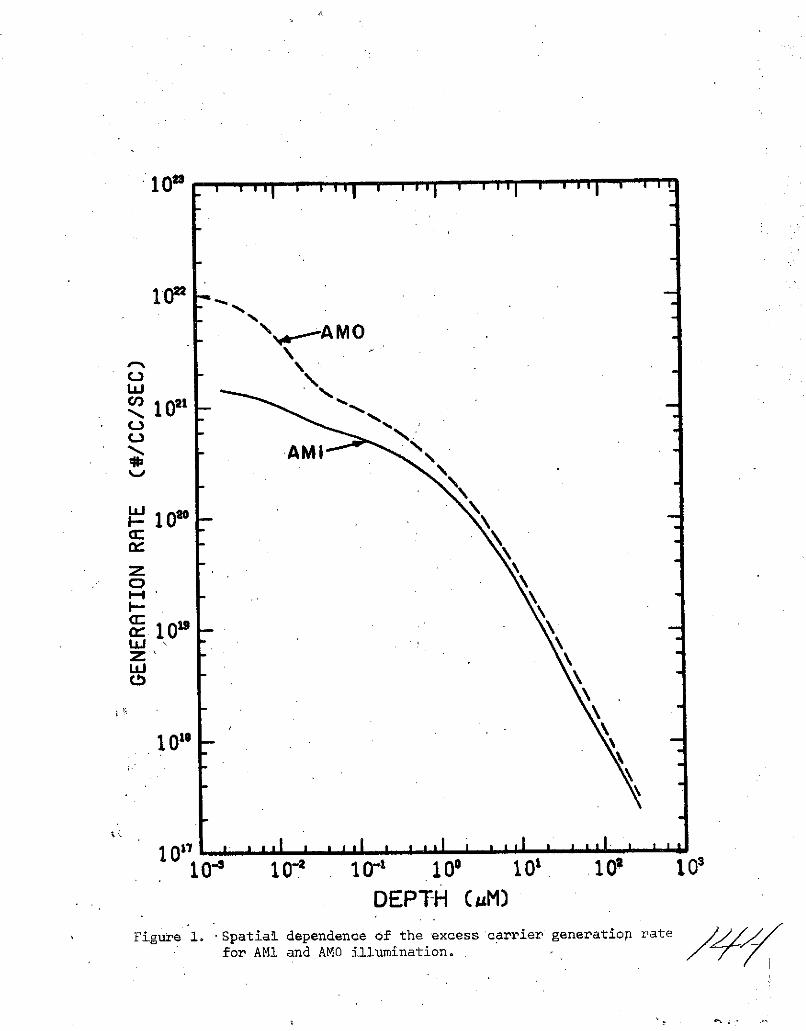
10 I "1, ' li"1 ' li ' U" Il II lul I I l
1022
C",,AMO
10"
S101
DEPTH (UM)
Figure 1. Spatial dependence of the excess carrier generatiop ratefor AM1 and AMO illumination.for AMi and AMO illumination. 6

C.0)
10200"
- -1
a:
o 101
1019
10 1 f ill a III a I a ll a a I I I II a a 0
10 1.0 10 100 101 102 103
DEPTH (aM)
Figure 2. Spatial'ependence of the excess carrier generation rate forboth. single layer SiO and SiO2 films at their optimumthickness.

100
R 90
0 80-z
U-
060o
W 50
40
30 50 100 150 200
TOTAL DEVICE LENGTH (g M)
Figure 3. Percentage of optical current collected versus device length. Although this curve is for AMO with
no ntireflection coating the other conditions have quite similar results.

ANTI-AIR REFLECTION SILICON
LAYER
nl=l n2-ikc2" n3-ik 3
Figure 4. Structure utilited.in the calculation of the opticalcoefficients.

" I I I I
o \ T, 1100 ,SSi \
S\T, d 0 i
'-
LL
\w
I-
OCOI)
C1 2 3 4 5 6 7
ENERGY. (EV)
Figure 5. Transmission coefficients fop silicon and silicon plusthe optimum thickness of Si02'

T
~I
C~ I
" L.
Co
w I
LIU--
SII . -
c" 2 3 4 5ENERGY (EV)
Figure 6. Transmission (T), Absorption (A), and Reflection (R)coefficients for optimum thickness of a single layerSiO film.
o I
SiO film.

85
SIO80-
75
500 1000 1500
FILM THICKNESS ( '
Figure 7. Efficiency of photon transmission into silicon versus film
thickness for both SiO and SiO 2.
-t

)cn
REAL PART, nI-0
- 2
LL0
IMAGINARY PART, kc
(EXTINCTION COEFFICIENT)
1 2 .3 4 5 6
ENERGY (ev)Figure 8. Real and imaginary parts of the index of refraction for Si [16].

DETERMINATION OF RUN CHARACTERISTIC
-MONOCHROMATIC
-AMO--AM1-NATURE OF ANTIREFLECTION LAYER
READING OF IRRADIANCE DATA
CALCULATION OF PHOTON INCIDENT DENSITY
READING OF DATA FOR ABSORPTION COEFFICIENT
AND THE REAL PART OF THE INDEX OFREFRACTION
INTERPOLATION OF OPTICAL PARAMETERS TOVALUES AT IRRADIANCE DATA WAVELENGTHS
CALCULATION OF TRANSMISSION PROPERTIESOF DE I RD SURFACE
N DATA CALCULATION OFSURFACE EFFICIENCY
DETERMINATION OF SPATIAL DISTRIBUTION
FOR EACH X SUM G OVER ALL WAVELENGTHSe
NUMERICAL. INTEGRATION OF G VERSUS X
END
Piure a. Flow chart for optical genetation program.
Appendix C: Minority Carrier Reflecting Properties of
Semiconductor High-Low Junctions
J. R. Hauser and P. M. DunbarElectrical Engineering Department
North Carolina State UniversityRaleigh, North Carolina 27607
ABSTRACT
This paper discusses the results of some..computer calculations
on the minority carrier reflecting properties of high-low junctions.
In general it has been found that high-low junctions obey first
order device models to a high degree of accuracy. The ratio of
carrier densities on the sides of the junction depletion region is
exponentially related to the high-low junction voltage, which is constant
until high injection effects begin to occur. For high injection on the
lightly doped side of the high-low junction, the junction potential
decreases and the minority carrier reflecting properties of the
junction are degraded.

I. INTRODUCTION
High-low junctions (either p -p or n -n) find a number of
applications in solid state devices. They are most frequently
used as an interface region between a more lightly doped semiconductor
and a metal contact in order to provide an ohmic contact to the
semiconductor. In this application they are known to provide an
essentially linear current-voltage relationship for majority carrier
flow across the high-low interface [1,21. In addition to aiding in
making ohmic contacts, high-low junctions also act as minority
carrier reflecting boundaries. In many minority carrier devices
this is a useful side effect which can significantly reduce minority
carrier recombination at ohmic contacts.
The present work reports on some computer solutions of the
minority carrier reflecting properties of high-low junctions which
are located near an injecting p-n junction. This work has resulted
+ +from a study of p -p-n type diode structures. However, the same
type of behavior should be observed at any high-low junction
located near an injecting p-n junction. A comparison is also presented
of first order analytical models for high-low junctions with the
exact computer solutions.

2
II. HIGH-LOW JUNCTION PROPERTIES
The device structure studied in this work is shown in Fig. 1.
It is an n -p-p diode with the n+ diffused layer modeled by a
20 3Gaussian impurity profile with a surface concentration of 1020/cm
and a junction depth of 0.25 pm. The p-region is taken as a uniformly
doped region with results for 10 Q*cm and 2000 2-cm material reported
in this work. The p region has been taken as a uniformly doped
region with an impurity concentration of 1018/cm3 and a thickness
of either 5 Um or 0.5 pm. The overall device thickness is 250 im
for the results reported in this paper.
The electron lifetime in the p-region was taken as 100 psec and
1000 psec for the 10 Q-cm and 2000 *cm material respectively. Other
device thicknesses have been studied but the total device thickness
does not strongly influence the minority carrier reflecting properties
of the p -p junction.
The device structures studied have been less than a diffusion
length in total thickness. The p -p interface thus acts as a minority
carrier reflecting boundary preventing electrons injected by the n -p
junction from reaching the back ohmic contact. Various injected electron
concentration profiles for this diode can appear as shown in Fig. 2 as
the back boundary ranges from a perfectly reflecting contact to an ohmic
contact. For the devices studied in this work the high-low junction
closely approximates an ideal reflecting back contact even for p+
thicknesses of 0.5 pm.
There are several parameters which characterize a high-low junction
as far as its minority carrier reflecting properties are concerned.

3
First, there is the equilibrium high-low junction voltage, Vhlo, which
is related to the doping densities as
V = -Tn (N +/N), ()hlo q p p
where N and N are the p+- and p-region doping densities. The high-
low junction potential can only change from its equilibrium value if
there is a significant change in the majority carrier concentration on
one or the other side of the high-low junction. A second fundamental
parameter is the ratio of minority carriers (electrons in this case)
across the junction. Assuming that the change in minority carrier
quasi-Fermi level is negligible across the interface gives El],
n , = n exp(-qVhl/kT). (2)
If high injection does not occur on the lightly doped p-side, Vhl is
approximately the equilibrium value and
n p = nN /N . (3)
This expression is the basis for the reflecting properties of the high-
low junction since it shows that the minority carrier concentration is
+reduced by the ratio N /N + in going from the p to p side of the
junction.
The expression of Equation (3) is based upon a low injection
condition. In the more general case, Equation (2) must be combined with
the assumption of charge neutrality at the edges of the junction depletion
region to give the following more complete expression:
n Nn + = n (1 + - 2) . (4)
P p N NP P

4
The additional correction factor of (1 + n p/N ) becomes important when
high injection occurs on the lightly doped side of the high-low junction.
A final parameter characterizing the minority carrier reflecting
properties of a high-low junction is what Gunn [3] terms the junction
leakage velocity or which can also be termed the effective surface
recombination velocity, S , of the high-low junction. As opposed to
the ratio of minority carriers across the interface which depends only
on the high-low junction doping levels, the leakage velocity depends
on the width of the p region and the minority carrier lifetime in ttis
region. For uniform doping in the p region and neglecting recombination
within the high-low junction space charge region,
S + = Dr coth ( p+) n (5)pp Lnp+ Lnp+ np
where Dnp+ and Lnp+ are the electron diffusion constant and diffusion
length in the p+ region. The above can be combined with Equation (4)
to give
D M W+ nS np p coth ( -)(1 + -2). (6)pp Lnp+ p+ np+ P
At low injection this is a constant but the value increases linearly
with n at high injection. This causes the minority carrier currentP
into the high-low junction to increase linearly with carrier density
n at low injection and to increase as n 2 at high injection.p p

5
III. COMPUTED RESULTS
The simple models discussed in the previous section have been
found to agree extremely well with exact computer calculations for
high-low junctions. The computer program used in the present device
analysis has been previously discussed E4]. Calculations have been
made for the structure of Fig. 1 for a variety of dimensions and
doping densities. Calculations are made at various terminal voltages
which result in increasing levels of carrier injection into the p-region.
Shown in Fig. 3 are curves for electron concentration plotted from the
back surface through the high-low junction for a 0.5 pm wide p region.
The electron concentration in the p-side ranges from slightly above
10 9/cm 3 to about 1016/cm 3 while the concentration on the p side ranges
4 3 14 3from about 10 /cm to about 1014/cm3. The VA values on the curves are
the values of applied diode voltage corresponding to each injection
level. For the low values of VA the junction depletion region extends
beyond 1.5 pm and the carrier densities are not yet constant. Shown
in Fig. 4 is the dependence of np+ on n for this device (curve A).
The solid curve is the simple model as given by Equation (4) while
the data points are results of the exact computer calculations. The
onset of high injection can be seen for the highest injection levels.
Calculations for a 5 pm wide p region are essentially identical
with the results shown in Fig. 4 with the ratio of minority carriers
across the high-low junction independent of the width of the p region.
Also shown in Fig. 4 are similar data (curve B) for a diode with a
p-side concentration of 1.3x10¹⁵/cm 3 . At high injection both curves
approach the same limiting values which are independent of p-side
doping density.

6
Under high injection conditions, the potential across the high-low
junction decreases from its equilibrium value. This is shown in Fig. 5
where the decrease in potential is seen for the four highest injection
levels. For curves (a) and (b) the junction depletion region extends
beyond 1.5 pm. As the junction potential decreases at high injection,
the ratio of minority carriers across the interface decreases and the
reflecting properties of the high-low junction are degraded. The
effective surface recombination velocity of the junction increases as
high injection occurs according to Equation (6).
Shown in Fig. 6 is a comparison of the high-low junction leakage
current as given-by the expression
nhl qnp pp (7)
and the exact results of the computer solutions. Again it is seen that
at low injection the leakage current is proportional to n indicating
a constant S + while at high injection the leakage current depends onpp
n2 indicating that S + approaches a linear dependence on n . Asp pp p
indicated in the figure, at low injection the high-low junction has a
low effective surface recombination velocity. The nearly
ideal minority carrier reflecting properties of these high-low junctions
is due to this low value of effective surface recombination velocity.
Similar high-low junctions but with a 5 pm thick p+ layer have about an
order of magnitude smaller effective surface recombination velocity.
Implicit in the derivation of Equations (3) and (4) is the
assumption that the minority carrier quasi-Fermi level does not change
in going across the high-low junction. This assumption has been verified
with the computer calculations. Shown in Fig. 7 is the calculated

7
quasi-Fermi levels for electrons n around the high-low junction. The
only change in n around the high-low junction is the almost abrupt.
change in slope of the pn curves at the high-low junction. This is
d4nto be-expected since must be inversely proportional to the electron
concentration in a region where there is negligible change in current
density.

8
IV. CONCLUSIONS
This work has reviewed the first order approximations normally
employed to describe the minority carrier reflecting properties of
high-low junctions and compared these expressions with exact computed
results. The first order results are found to be in very good agree-
ment with the computer results when account is taken of high injection
effects on the lightly doped side of the high-low junction. High
injection reduces the effectiveness of the high-low junction as a
minority carrier reflecting boundary and leads to an increased
effective surface recombination velocity of the junction.

9
REFERENCES
1. J. B. Gunn, "On Carrier Accumulation and the Properties of Certain
Semiconductor Junctions," J. Electronic Control, vol. 4, p. 17, 1958.
2. R. W. Lade and A. G. Jordan, "A Study of Ohmicity and Exclusion
in High-Low Semiconductor Junction Devices," IEEE Trans. Electron
Devices, vol. ED-10, pp 268-277, July 1963.
3. R. W. Dutton and R. J. Whittier, "Forward Current-Valtage and SwitchingCharacteristics of p+-n-n+ (Epitaxial) Diodes", IEEE Trans. Electron
Devices, vol. ED-16, pp. 458-467, May 1969.
4. E. D. Graham, Jr. and J. R. Hauser, "Effects of Base Doping and
Width on the J-V Characteristics of the n+-n-p+ Structure",
Solid-State Elec. vol. 15, pp 303-310, 1972.

10
FIGURE CAPTIONS
Fig. 1. Device structure for n -p-D diode (A) 10000-cm p-region,N = 7xl012/cm3 , N = 10 1/cm3 (B) 100-cm p-region,
N = 1.3xl01 3/cm3, N + = 101 8/cm3 .P
Fig. 2. Effect of back contact on injected electron concentration
(W <<L ); (a) Ideal reflecting back contact (b) partiallyp n
reflecting back contact (c) ohmic contact.
Fig. 3. Calculated minority carrier concentration around the high-lowjunction at various injection levels (1000 Q.cm p-region).
Fig. 4. Minority carrier concentration at edge of depletion regionin p+-side as a function of minority carrier concentrationat edge of depletion region on p-side. The solid curvesare simple calculations from Eq. (4), while the data pointsare results of computer analysis,
Fig. 5. Electrostatic potential around high-low junction at variousinjection levels (1000 Q.cm p-region).
Fig. 6. High-low junction leakage current as a function of injectionlevel on p-side of.junction. The solid curves are simplecalculations from Eqs. (6) and (7) while the data points areresults of computer analysis.
Fig. 7. Electron quasi-Fermi level variation around high-low junction(1000 0.cm p-region).

n+
Sp Wt
+ +Fig. 1. Device structure for n -p-p diode (A) 1000, cm p-region,
12 3 18 3N = 7xl0 /cm N + = 10 /cm (B) 10-cm p-region,
p 13 3 18 3N 1.3x10 /cm , N = 10 /cm.
P P

(x)x
Fig. 2. Effect of back contact on injected electron concentration
(W <<L ); Ca) Ideal.reflecting back contact (b) partiallyreflecting ack contact (c) ohmic
reflecting back contact (c) ohmic contact.

1020
10 -
VA= 0.7v
0.60.5
0.4
0
101
S0.50 1.0 1.5
o-J - -
0 0.50 1.0 1.5LENGTH FROM P' SURFACE (uM)
Fig. 3. Calculated minority carrier concentration around the high-lowjunction at various injection levels (1000 0-cm p-region).
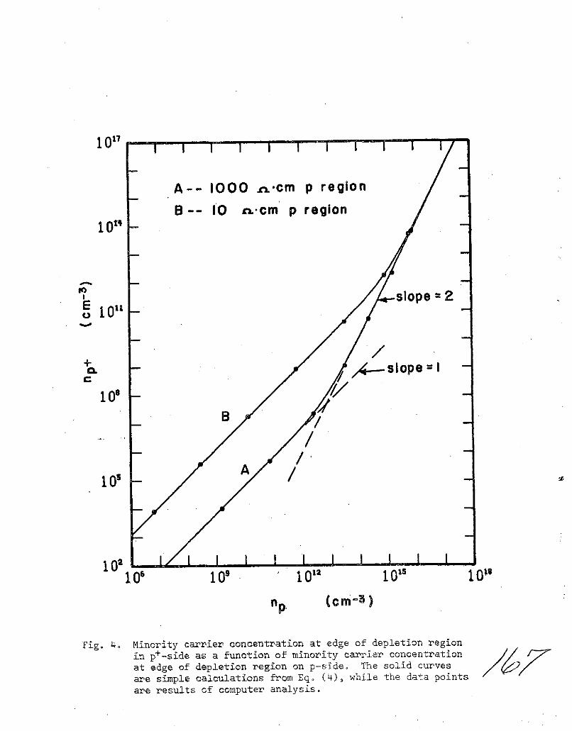
1017
A-- 1000 n..cm p region
B -- 10 r.-cm p region10"
slope -- 21011
S0 sIope I
1 0/
105 /
102 1 1210 10' 1 " 0 10
n . (cm- 3 )
Fig. 4. Minority carrier concentration at edge of depletion region
in p+-side as a function of minority carrier concentrationat edge of depletion region on p-side. The solid curvesare simple calculations from Eq. (4), while the data pointsare results of computer analysis.

Cr)
-I
o Icr
L)
F-u..J
I--1
oe:CI--
b-- np=3.21 x 10¹³
Ll C-- np = 2.27 x 10¹⁴
U.J d-- n 1.60 x 10¹⁵. ) PC e-- np= 7.69 x 10¹⁵
00o 0.50 1.0 .sLENGTH FROM P+ SURFACE (MM)
Fig. 5. Electrostatic potential around high-low junction at variousinjection levels (1000 *ocm p-regio)°
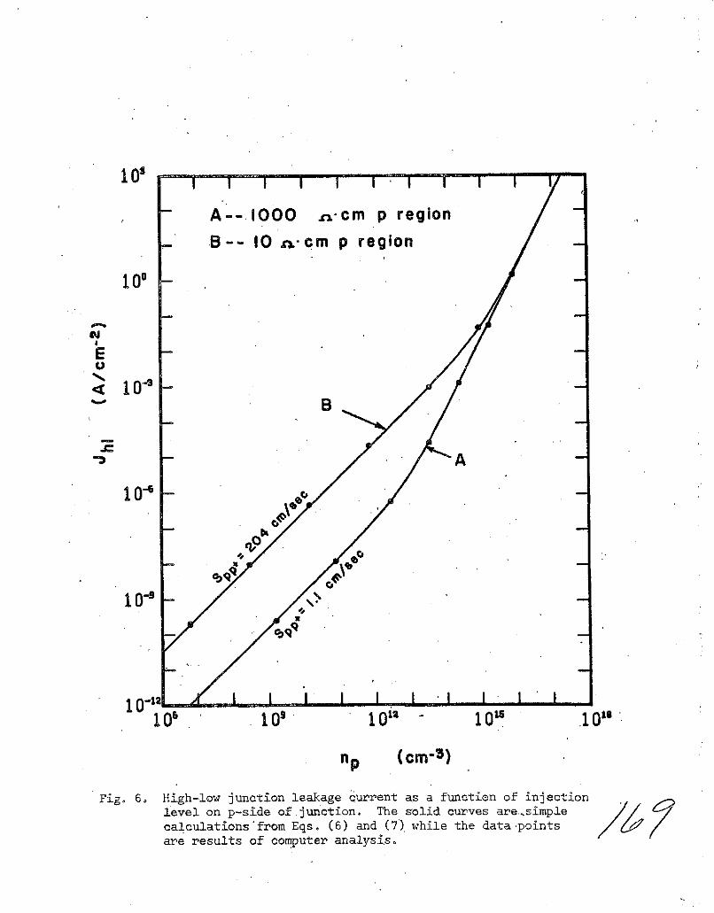
10'
A--. 1000 x-cm p region
B -- 10 .- cm p region
100
B
A
10-6 -
100C
1 or 10 10 - 105 1
n p (cm-3 )
Fig. 6. High-low junction leakage qurrent as a function of injectionlevel on p-side of junction. The solid curves are.simplecalculations'from Eqs. (6) and (7) while the data pointsare results of computer analysis.

I. _
Cd 0.2
0.,c)
0•
0.5LL
a:
coz -0.7
LU'
o I
0 0.50 1.0 1.5LENGTH FROM P* SURFACE (aCM)
'Fig. 7. Electron quasi-Fermi level variation around high-low junction(1000 0 cm p-region).