Embed Size (px)
Citation preview
IEEE JOURNAL OF SOLID-STATE CIRCUITS, VOL. 47, NO. 1, JANUARY 2012 23
A Super-Pipelined Energy Efficient Subthreshold240 MS/s FFT Core in 65 nm CMOS
Dongsuk Jeon, Student Member, IEEE, Mingoo Seok, Student Member, IEEE, Chaitali Chakrabarti,David Blaauw, Senior Member, IEEE, and Dennis Sylvester, Fellow, IEEE
Abstract—This paper proposes a design approach targetingcircuits operating at extremely low supply voltages, with thegoal of reducing the voltage at which energy is minimized,thereby improving the achievable energy efficiency of the circuit.The proposed methods accomplish this by minimizing the cir-cuit’s ratio of leakage to active current. The first method, superpipelining, increases the number of pipeline stages comparedto conventional ultra low voltage (ULV) pipelining strategies,reducing the leakage/dynamic energy ratio and simultaneouslyimproving performance and energy efficiency. Measurements ofsuper-pipelined multipliers demonstrate 30% energy savings and1.6 performance improvement. Since super pipelining reducesthe logic depth between registers, two-phase latch based design isemployed to compensate for reduced averaging effects and pro-vide better variation tolerance. The second technique introduces aparallel-pipelined architecture that suppresses leakage energy byensuring full utilization of functional units and reduces memorysize. We apply these techniques to a 16-b 1024-pt complex-valuedFast Fourier Transform (FFT) core along with low-power first-infirst-out (FIFO) design and robust clock distribution network.The FFT core is fabricated in 65 nm CMOS and consumes15.8 nJ/FFT with a clock frequency of 30 MHz and throughputof 240 Msamples/s at ��� � ��� ��, providing 2.4 betterenergy efficiency than current state-of-art and �� higherthroughput than typical ULV designs. Measurements of 60 diesshow modest frequency (energy) spreads of 7% (2%).
Index Terms—Fast Fourier Transform (FFT), subthresholdCMOS circuits, super-pipelining, ultra low voltage (ULV) design.
I. INTRODUCTION
R ECENTLY, voltage scaling has been widely applied tohighly energy-constrained systems such as battery-pow-
ered sensor nodes to minimize energy consumption. Voltagescaling enables energy efficient computation by quadratic (orgreater) reductions of switching and leakage power dissipa-tion. Although voltage scaling increases gate delay and thusdegrades performance, it is still advantageous for many appli-cations with relaxed performance requirements [1], [2] and thesupply voltage may be scaled down to, or below, the devicethreshold voltage . However, leakage energy consumption
Manuscript received April 22, 2011; revised June 27, 2011; accepted August22, 2011. Date of publication November 04, 2011; date of current version De-cember 23, 2011. This paper was approved by Guest Editor Tanay Karnik. Thiswork was supported by the Multiscale Systems Center, Army Research Lab-oratory, National Science Foundation, and National Institute of Standards andTechnology.
D. Jeon, D. Blaauw, and D. Sylvester are with the University of Michigan,Ann Arbor, MI 48109-2121 USA (e-mail: [email protected]).
M. Seok is with Texas Instruments, Dallas, TX 75243 USA.C. Chakrabarti is with Arizona State University, Tempe, AZ 85287 USA.Digital Object Identifier 10.1109/JSSC.2011.2169311
per cycle increases due to enlarged stage delay as voltagescales and this overhead starts to exceed the switching energysavings below the optimal operating point , producingoptimal energy consumption . Therefore there exists afundamental limit for energy savings from voltage scaling inthe subthreshold regime regardless of [3]. To enhanceenergy efficiency beyond this point, leakage energy must besuppressed by elimination of idle gates or other techniques toboost the utilization of each gate or module in the system. Sinceultra-low voltage operation incurs high process/voltage/tem-perature (PVT) variation [4], variation tolerance should alsobe considered in designing these low voltage systems. Such anenergy-optimal design methodology is demonstrated on a FastFourier Transform (FFT) accelerator in this work.
The FFT is a key digital signal processing (DSP) algorithmand is widely used in digital communication and sensor signalprocessing. Aided by technology scaling, FFT accelerators havebecome feasible, offering higher energy efficiency than gen-eral purpose processors even for volume-constrained systemssuch as sensor nodes [2], [5]. We use such an FFT core as ademonstration vehicle for several circuit and architectural tech-niques aimed at reducing and , while achieving un-usually high throughput for a subthreshold circuit. Past workin power efficient FFTs include [6], where the authors proposea cached-memory FFT architecture that processes intermediateresults within cached data sets to minimize the number of mainmemory accesses. In [5], the authors employ voltage scaling toimprove energy efficiency. They use standard cells and mem-ories optimized for subthreshold operation and target their de-sign at the optimal energy operating point. However, the bodyof prior work in this area has not investigated the key role ofleakage energy in the subthreshold regime, and we show thatenergy efficiency can be improved beyond the conventional op-timal energy operating point by suppressing leakage effectively.
This paper is an extension of [7]. It describes the use ofvarious circuit techniques such as super-pipelining along withan architectural study focused on extending voltage scalabilityand enhancing performance in the design of 1024-point com-plex-valued FFT core. The use of super-pipelining improvesperformance and reduces leakage energy, but removes aver-aging effects of random process variability due to shorter logicdepth. As a result we employ two-phase latches rather thanedge-triggered registers to recapture some averaging throughtime borrowing. Measured results of these techniques on amultiplier show 30% energy savings concurrently with 1.6performance improvement over a conventional unpipelinedmultiplier. A parallel-pipelined FFT architecture is thenproposed to maximize computational element and memory
0018-9200/$26.00 © 2011 IEEE
24 IEEE JOURNAL OF SOLID-STATE CIRCUITS, VOL. 47, NO. 1, JANUARY 2012
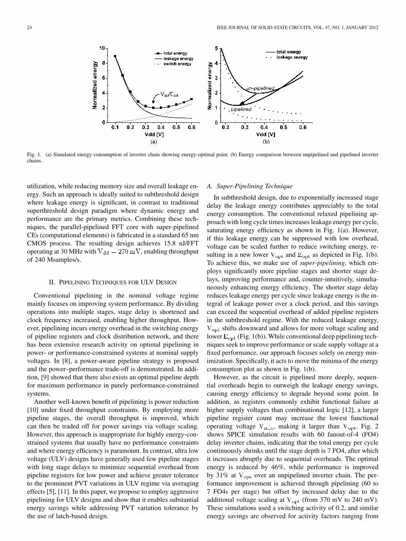
Fig. 1. (a) Simulated energy consumption of inverter chain showing energy-optimal point. (b) Energy comparison between unpipelined and pipelined inverterchains.
utilization, while reducing memory size and overall leakage en-ergy. Such an approach is ideally suited to subthreshold designwhere leakage energy is significant, in contrast to traditionalsuperthreshold design paradigm where dynamic energy andperformance are the primary metrics. Combining these tech-niques, the parallel-pipelined FFT core with super-pipelinedCEs (computational elements) is fabricated in a standard 65 nmCMOS process. The resulting design achieves 15.8 nJ/FFToperating at 30 MHz with , enabling throughputof 240 Msamples/s.
II. PIPELINING TECHNIQUES FOR ULV DESIGN
Conventional pipelining in the nominal voltage regimemainly focuses on improving system performance. By dividingoperations into multiple stages, stage delay is shortened andclock frequency increased, enabling higher throughput. How-ever, pipelining incurs energy overhead in the switching energyof pipeline registers and clock distribution network, and therehas been extensive research activity on optimal pipelining inpower- or performance-constrained systems at nominal supplyvoltages. In [8], a power-aware pipeline strategy is proposedand the power–performance trade-off is demonstrated. In addi-tion, [9] showed that there also exists an optimal pipeline depthfor maximum performance in purely performance-constrainedsystems.
Another well-known benefit of pipelining is power reduction[10] under fixed throughput constraints. By employing morepipeline stages, the overall throughput is improved, whichcan then be traded off for power savings via voltage scaling.However, this approach is inappropriate for highly energy-con-strained systems that usually have no performance constraintsand where energy efficiency is paramount. In contrast, ultra lowvoltage (ULV) designs have generally used few pipeline stageswith long stage delays to minimize sequential overhead frompipeline registers for low power and achieve greater toleranceto the prominent PVT variations in ULV regime via averagingeffects [5], [11]. In this paper, we propose to employ aggressivepipelining for ULV designs and show that it enables substantialenergy savings while addressing PVT variation tolerance bythe use of latch-based design.
A. Super-Pipelining Technique
In subthreshold design, due to exponentially increased stagedelay the leakage energy contributes appreciably to the totalenergy consumption. The conventional relaxed pipelining ap-proach with long cycle times increases leakage energy per cycle,saturating energy efficiency as shown in Fig. 1(a). However,if this leakage energy can be suppressed with low overhead,voltage can be scaled further to reduce switching energy, re-sulting in a new lower and as depicted in Fig. 1(b).To achieve this, we make use of super-pipelining, which em-ploys significantly more pipeline stages and shorter stage de-lays, improving performance and, counter-intuitively, simulta-neously enhancing energy efficiency. The shorter stage delayreduces leakage energy per cycle since leakage energy is the in-tegral of leakage power over a clock period, and this savingscan exceed the sequential overhead of added pipeline registersin the subthreshold regime. With the reduced leakage energy,
shifts downward and allows for more voltage scaling andlower (Fig. 1(b)). While conventional deep pipelining tech-niques seek to improve performance or scale supply voltage at afixed performance, our approach focuses solely on energy min-imization. Specifically, it acts to move the minima of the energyconsumption plot as shown in Fig. 1(b).
However, as the circuit is pipelined more deeply, sequen-tial overheads begin to outweigh the leakage energy savings,causing energy efficiency to degrade beyond some point. Inaddition, as registers commonly exhibit functional failure athigher supply voltages than combinational logic [12], a largerpipeline register count may increase the lowest functionaloperating voltage , making it larger than . Fig. 2shows SPICE simulation results with 60 fanout-of-4 (FO4)delay inverter chains, indicating that the total energy per cyclecontinuously shrinks until the stage depth is 7 FO4, after whichit increases abruptly due to sequential overheads. The optimalenergy is reduced by 46%, while performance is improvedby 31% at over an unpipelined inverter chain. The per-formance improvement is achieved through pipelining (60 to7 FO4s per stage) but offset by increased delay due to theadditional voltage scaling at (from 370 mV to 240 mV).These simulations used a switching activity of 0.2, and similarenergy savings are observed for activity factors ranging from
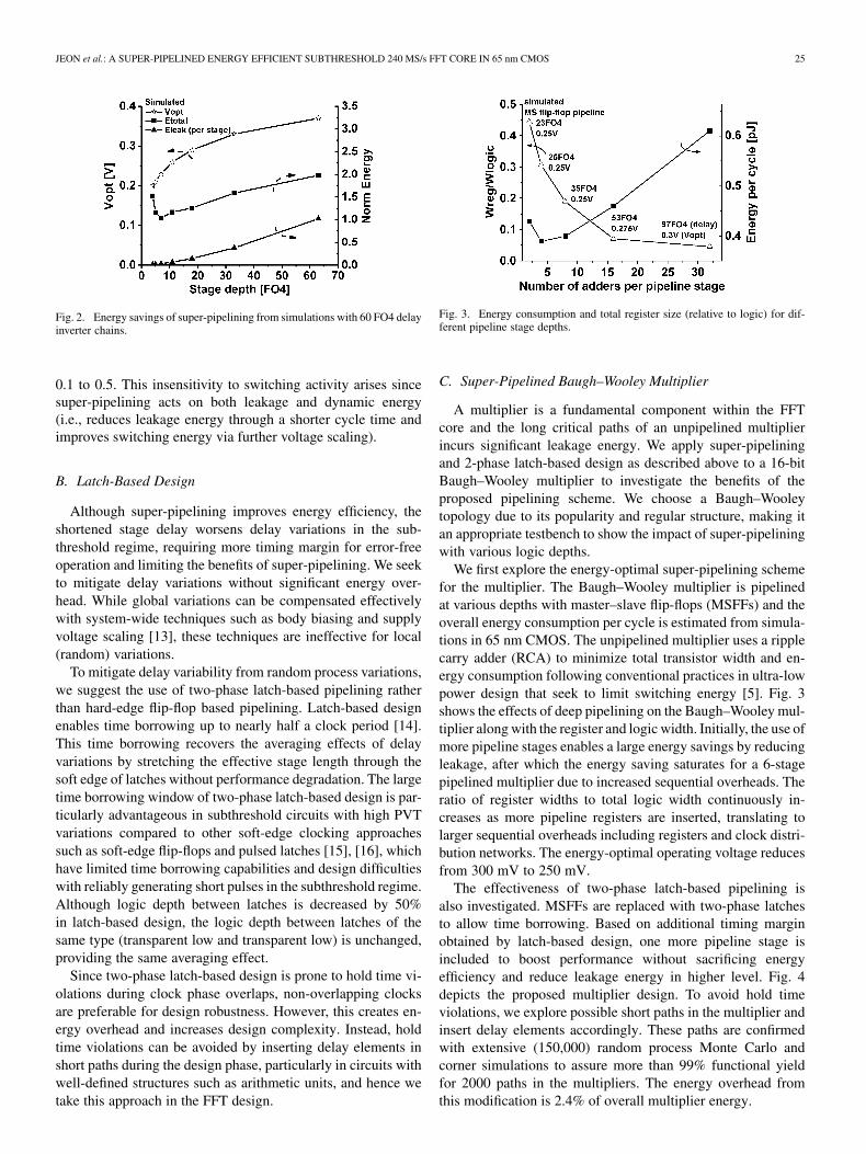
JEON et al.: A SUPER-PIPELINED ENERGY EFFICIENT SUBTHRESHOLD 240 MS/s FFT CORE IN 65 nm CMOS 25
Fig. 2. Energy savings of super-pipelining from simulations with 60 FO4 delayinverter chains.
0.1 to 0.5. This insensitivity to switching activity arises sincesuper-pipelining acts on both leakage and dynamic energy(i.e., reduces leakage energy through a shorter cycle time andimproves switching energy via further voltage scaling).
B. Latch-Based Design
Although super-pipelining improves energy efficiency, theshortened stage delay worsens delay variations in the sub-threshold regime, requiring more timing margin for error-freeoperation and limiting the benefits of super-pipelining. We seekto mitigate delay variations without significant energy over-head. While global variations can be compensated effectivelywith system-wide techniques such as body biasing and supplyvoltage scaling [13], these techniques are ineffective for local(random) variations.
To mitigate delay variability from random process variations,we suggest the use of two-phase latch-based pipelining ratherthan hard-edge flip-flop based pipelining. Latch-based designenables time borrowing up to nearly half a clock period [14].This time borrowing recovers the averaging effects of delayvariations by stretching the effective stage length through thesoft edge of latches without performance degradation. The largetime borrowing window of two-phase latch-based design is par-ticularly advantageous in subthreshold circuits with high PVTvariations compared to other soft-edge clocking approachessuch as soft-edge flip-flops and pulsed latches [15], [16], whichhave limited time borrowing capabilities and design difficultieswith reliably generating short pulses in the subthreshold regime.Although logic depth between latches is decreased by 50%in latch-based design, the logic depth between latches of thesame type (transparent low and transparent low) is unchanged,providing the same averaging effect.
Since two-phase latch-based design is prone to hold time vi-olations during clock phase overlaps, non-overlapping clocksare preferable for design robustness. However, this creates en-ergy overhead and increases design complexity. Instead, holdtime violations can be avoided by inserting delay elements inshort paths during the design phase, particularly in circuits withwell-defined structures such as arithmetic units, and hence wetake this approach in the FFT design.
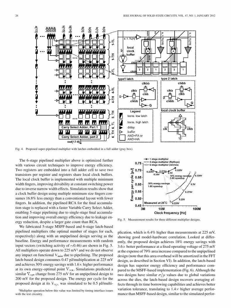
Fig. 3. Energy consumption and total register size (relative to logic) for dif-ferent pipeline stage depths.
C. Super-Pipelined Baugh–Wooley Multiplier
A multiplier is a fundamental component within the FFTcore and the long critical paths of an unpipelined multiplierincurs significant leakage energy. We apply super-pipeliningand 2-phase latch-based design as described above to a 16-bitBaugh–Wooley multiplier to investigate the benefits of theproposed pipelining scheme. We choose a Baugh–Wooleytopology due to its popularity and regular structure, making itan appropriate testbench to show the impact of super-pipeliningwith various logic depths.
We first explore the energy-optimal super-pipelining schemefor the multiplier. The Baugh–Wooley multiplier is pipelinedat various depths with master–slave flip-flops (MSFFs) and theoverall energy consumption per cycle is estimated from simula-tions in 65 nm CMOS. The unpipelined multiplier uses a ripplecarry adder (RCA) to minimize total transistor width and en-ergy consumption following conventional practices in ultra-lowpower design that seek to limit switching energy [5]. Fig. 3shows the effects of deep pipelining on the Baugh–Wooley mul-tiplier along with the register and logic width. Initially, the use ofmore pipeline stages enables a large energy savings by reducingleakage, after which the energy saving saturates for a 6-stagepipelined multiplier due to increased sequential overheads. Theratio of register widths to total logic width continuously in-creases as more pipeline registers are inserted, translating tolarger sequential overheads including registers and clock distri-bution networks. The energy-optimal operating voltage reducesfrom 300 mV to 250 mV.
The effectiveness of two-phase latch-based pipelining isalso investigated. MSFFs are replaced with two-phase latchesto allow time borrowing. Based on additional timing marginobtained by latch-based design, one more pipeline stage isincluded to boost performance without sacrificing energyefficiency and reduce leakage energy in higher level. Fig. 4depicts the proposed multiplier design. To avoid hold timeviolations, we explore possible short paths in the multiplier andinsert delay elements accordingly. These paths are confirmedwith extensive (150,000) random process Monte Carlo andcorner simulations to assure more than 99% functional yieldfor 2000 paths in the multipliers. The energy overhead fromthis modification is 2.4% of overall multiplier energy.
26 IEEE JOURNAL OF SOLID-STATE CIRCUITS, VOL. 47, NO. 1, JANUARY 2012
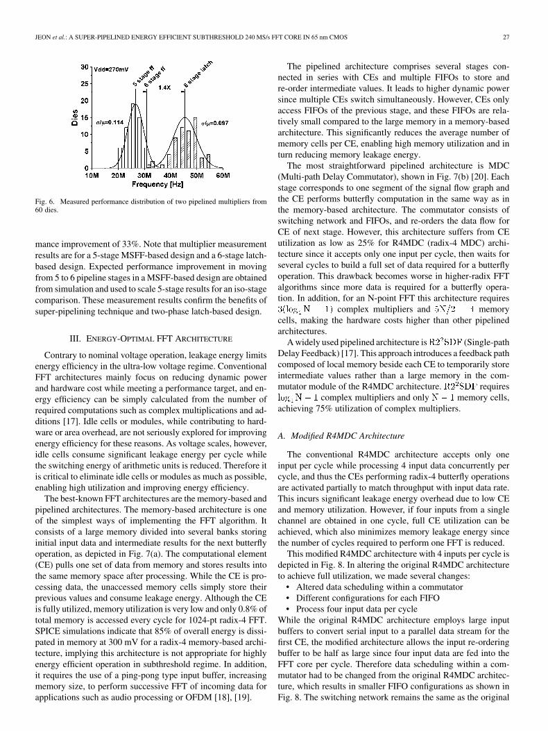
Fig. 4. Proposed super-pipelined multiplier with latches embedded in a full adder (gray box).
The 6-stage pipelined multiplier above is optimized furtherwith various circuit techniques to improve energy efficiency.Two registers are embedded into a full adder cell to save twotransistors per register and registers share local clock buffers.The local clock buffer is implemented with multiple minimumwidth fingers, improving drivability at constant switching powerdue to inverse narrow width effects. Simulation results show thata clock buffer design using multiple minimum size fingers con-sumes 16.8% less energy than a conventional layout with fewerfingers. In addition, the pipelined RCA for the final accumula-tion stage is replaced with a faster Variable Carry Select Adder,enabling 5-stage pipelining due to single-stage final accumula-tion and improving overall energy efficiency due to leakage en-ergy reduction, despite a larger gate count than RCA.
We fabricated 5-stage MSFF-based and 6-stage latch-basedpipelined multipliers (the optimal number of stages for each,respectively) along with an unpipelined design serving as thebaseline. Energy and performance measurements with randominput vectors (switching activity of 0.46) are shown in Fig. 5.All multipliers operate down to 225 mV1 and we do not observeany impact on functional due to pipelining. The proposedlatch-based design consumes 0.47 pJ/multiplication at 225 mVand achieves 30% energy savings with 1.6 higher performanceat its own energy-optimal point . Simulations predicted asimilar change from 275 mV for an unpipelined design to200 mV for the proposed design. The energy per cycle for theproposed design at its was simulated to be 0.5 pJ/multi-
1Multiplier operation below this value was limited by timing interface issueswith the test circuitry.
Fig. 5. Measurement results for three different multiplier designs.
plication, which is 6.4% higher than measurements at 225 mV,showing good model-hardware correlation. Looked at differ-ently, the proposed design achieves 18% energy savings with3.6 better performance at a fixed operating voltage of 275 mVat the expense of 79% area increase compared to the unpipelineddesign (note that this area overhead will be amortized in the FFTdesign, as described in Section VI). In addition, the latch-baseddesign has superior energy efficiency and performance com-pared to the MSFF-based implementation (Fig. 6). Although thetwo designs have similar values due to global variationsacross the dies, the latch-based design recovers averaging ef-fects through its time borrowing capabilities and achieves bettervariation tolerance, translating to 1.4 higher average perfor-mance than MSFF-based design, similar to the simulated perfor-
JEON et al.: A SUPER-PIPELINED ENERGY EFFICIENT SUBTHRESHOLD 240 MS/s FFT CORE IN 65 nm CMOS 27
Fig. 6. Measured performance distribution of two pipelined multipliers from60 dies.
mance improvement of 33%. Note that multiplier measurementresults are for a 5-stage MSFF-based design and a 6-stage latch-based design. Expected performance improvement in movingfrom 5 to 6 pipeline stages in a MSFF-based design are obtainedfrom simulation and used to scale 5-stage results for an iso-stagecomparison. These measurement results confirm the benefits ofsuper-pipelining technique and two-phase latch-based design.
III. ENERGY-OPTIMAL FFT ARCHITECTURE
Contrary to nominal voltage operation, leakage energy limitsenergy efficiency in the ultra-low voltage regime. ConventionalFFT architectures mainly focus on reducing dynamic powerand hardware cost while meeting a performance target, and en-ergy efficiency can be simply calculated from the number ofrequired computations such as complex multiplications and ad-ditions [17]. Idle cells or modules, while contributing to hard-ware or area overhead, are not seriously explored for improvingenergy efficiency for these reasons. As voltage scales, however,idle cells consume significant leakage energy per cycle whilethe switching energy of arithmetic units is reduced. Therefore itis critical to eliminate idle cells or modules as much as possible,enabling high utilization and improving energy efficiency.
The best-known FFT architectures are the memory-based andpipelined architectures. The memory-based architecture is oneof the simplest ways of implementing the FFT algorithm. Itconsists of a large memory divided into several banks storinginitial input data and intermediate results for the next butterflyoperation, as depicted in Fig. 7(a). The computational element(CE) pulls one set of data from memory and stores results intothe same memory space after processing. While the CE is pro-cessing data, the unaccessed memory cells simply store theirprevious values and consume leakage energy. Although the CEis fully utilized, memory utilization is very low and only 0.8% oftotal memory is accessed every cycle for 1024-pt radix-4 FFT.SPICE simulations indicate that 85% of overall energy is dissi-pated in memory at 300 mV for a radix-4 memory-based archi-tecture, implying this architecture is not appropriate for highlyenergy efficient operation in subthreshold regime. In addition,it requires the use of a ping-pong type input buffer, increasingmemory size, to perform successive FFT of incoming data forapplications such as audio processing or OFDM [18], [19].
The pipelined architecture comprises several stages con-nected in series with CEs and multiple FIFOs to store andre-order intermediate values. It leads to higher dynamic powersince multiple CEs switch simultaneously. However, CEs onlyaccess FIFOs of the previous stage, and these FIFOs are rela-tively small compared to the large memory in a memory-basedarchitecture. This significantly reduces the average number ofmemory cells per CE, enabling high memory utilization and inturn reducing memory leakage energy.
The most straightforward pipelined architecture is MDC(Multi-path Delay Commutator), shown in Fig. 7(b) [20]. Eachstage corresponds to one segment of the signal flow graph andthe CE performs butterfly computation in the same way as inthe memory-based architecture. The commutator consists ofswitching network and FIFOs, and re-orders the data flow forCE of next stage. However, this architecture suffers from CEutilization as low as 25% for R4MDC (radix-4 MDC) archi-tecture since it accepts only one input per cycle, then waits forseveral cycles to build a full set of data required for a butterflyoperation. This drawback becomes worse in higher-radix FFTalgorithms since more data is required for a butterfly opera-tion. In addition, for an N-point FFT this architecture requires
complex multipliers and memorycells, making the hardware costs higher than other pipelinedarchitectures.
A widely used pipelined architecture is (Single-pathDelay Feedback) [17]. This approach introduces a feedback pathcomposed of local memory beside each CE to temporarily storeintermediate values rather than a large memory in the com-mutator module of the R4MDC architecture. requires
complex multipliers and only memory cells,achieving 75% utilization of complex multipliers.
A. Modified R4MDC Architecture
The conventional R4MDC architecture accepts only oneinput per cycle while processing 4 input data concurrently percycle, and thus the CEs performing radix-4 butterfly operationsare activated partially to match throughput with input data rate.This incurs significant leakage energy overhead due to low CEand memory utilization. However, if four inputs from a singlechannel are obtained in one cycle, full CE utilization can beachieved, which also minimizes memory leakage energy sincethe number of cycles required to perform one FFT is reduced.
This modified R4MDC architecture with 4 inputs per cycle isdepicted in Fig. 8. In altering the original R4MDC architectureto achieve full utilization, we made several changes:
• Altered data scheduling within a commutator• Different configurations for each FIFO• Process four input data per cycle
While the original R4MDC architecture employs large inputbuffers to convert serial input to a parallel data stream for thefirst CE, the modified architecture allows the input re-orderingbuffer to be half as large since four input data are fed into theFFT core per cycle. Therefore data scheduling within a com-mutator had to be changed from the original R4MDC architec-ture, which results in smaller FIFO configurations as shown inFig. 8. The switching network remains the same as the original

28 IEEE JOURNAL OF SOLID-STATE CIRCUITS, VOL. 47, NO. 1, JANUARY 2012
Fig. 7. (a) Memory-based architecture and (b) R4MDC pipelined architecture.
Fig. 8. Modified R4MDC architecture for 1024-pt FFT.
Fig. 9. Proposed FFT core architecture with two processing lanes.
R4MDC and a look-up table for twiddle factors is embedded ineach CE along with a controller.
In addition to full CE utilization, this architecture requiresfewer memory cells for commutators. Specifically, modifiedR4MDC contains memory cells compared toin R4MDC, reducing memory size by 30% for a 1024-pt FFT.Although a CE accesses memory every cycle, implying fullmemory utilization, this does not reflect the actual numberof activated versus idle cells. Instead the average number ofmemory cells per complex multiplier can be used as an alternatemetric in energy-constrained applications. For a 1024-pt FFT,the modified R4MDC requires 149 cells per complex multiplierwhile needs 255.75 cells (72% more). Taken together,modified R4MDC achieves 4 higher throughput and moreenergy efficient operation than with smaller hard-ware cost. Simulation results indicate that modified R4MDC
and consume 52% and 68% of their total energyin memory at 250 mV, respectively, with modified R4MDCconsuming 43.2% less energy with 2.6 better performancethan at their respective energy-optimal points.
B. Parallel-Pipelined Architecture
The improvements above significantly increase memory uti-lization and suppress leakage energy. However, even the mod-ified R4MDC architecture consumes 52% of its total energy inmemory, indicating that further room for improvement exists inmemory utilization. This section shows that FFT architectureparallelization reduces energy consumption per operation andimproves performance simultaneously.
Fig. 9 shows the modified R4MDC architecture with two pro-cessing lanes in parallel. Eight in-order input data are fed intothe FFT core every cycle and each processing lane processes

JEON et al.: A SUPER-PIPELINED ENERGY EFFICIENT SUBTHRESHOLD 240 MS/s FFT CORE IN 65 nm CMOS 29
Fig. 10. (a) Energy breakdown and (b) energy–area trade-off of parallel-pipelined architectures.
data within its own data set until the second stage from thelast, after which intermediate results are exchanged followedby independent processing in each lane. The proposed design inFig. 9 requires memory cells, similar to the 1-lane ver-sion. Thus, the average number of memory cells per multiplieris reduced by more than 50%, translating directly to memoryleakage reduction. The proposed design improves performanceby 2 through parallelism while consuming only 35% of itstotal energy in memory, indicating a greater degree of voltagescalability and potential improvements.
Area–time–energy optimization has been applied in a FIRfilter [21] previously to improve energy efficiency with fixedthroughput. The proposed FFT architecture differs from thiswork in that it focuses solely on achieving minimum energyconsumption with emphasis on the role of leakage current inthe subthreshold regime. Since ultra-low voltage (subthreshold)FFT architectures consume most of their energy in memory asleakage, the enhanced memory utilization from the proposed ar-chitecture provides significant energy savings.
The FFT core can be further parallelized to achieve continuedbenefits. However, hardware costs increase while the benefitfrom parallelization saturates as the CE active energy starts todominate. Fig. 10(a) shows energy breakdowns of modifiedR4MDC architectures with different degrees of parallelism.With the CE already fully utilized, its energy consumptionremains unchanged while memory energy decreases withadditional parallelization. The energy–area trade-off shown inFig. 10(b) clearly indicates that energy reductions from aggres-sive parallelism saturate while incurring large area overhead.Although the minimum energy will be achieved when entiresignal flow of FFT algorithm is implemented without anymemory modules, increased numbers of multipliers and othermodules results in higher PVT-induced variability and lowermaximum operating frequency, translating to more leakageenergy per cycle. In addition, higher parallelism incurs wireoverheads including the switching network and input/outputinterfaces. Based on this and available silicon area constraints,we implement the 2-lane version.
Simulation results show that the proposed design with 2 lanesconsumes 27.5% less energy with 2 higher performance thana 1-lane version, translating to 2.4 better energy efficiency
and 5.2 higher throughput than the conventionalarchitecture.
IV. ROBUST SUBTHRESHOLD FIFO DESIGN
The first-in first-out (FIFO) is a key module in commutators,and the proposed architecture employs a large number of thesemodules. Simulations of the 2-lane modified R4MDC architec-ture show that FIFOs consume up to 29% of total energy, makingit necessary to explore energy efficient FIFO design.
The most straightforward FIFO implementation is a shift reg-ister-based FIFO [22]. For an N delay FIFO, N registers are con-nected in series and all of them switch every cycle, sending datato next stage. Although this is very robust due to its negativehold time property, registers toggling every cycle have signifi-cant switching power overhead, making them less attractive forlow power designs. Another possible candidate for a low-powerFIFO is an SRAM-based design [23], which uses conventionalSRAM for storing data and reads data from each word succes-sively, writing subsequent data into the same address. For nom-inal voltage operation, a simple 6T SRAM can be used for highdensity with lower switching power than shift registers whileretaining sufficient speed to match the data rate. However, a 6TSRAM is not suitable for the subthreshold regime due to its sus-ceptibility to process variability and resulting small read/writemargins, and variants such as 10T [24] are preferred for robustoperation. The maximum operating frequency of robust sub-threshold SRAM designs is typically below 1 MHz [25], [26],making it impossible to meet performance requirements of ourtarget FFT design.
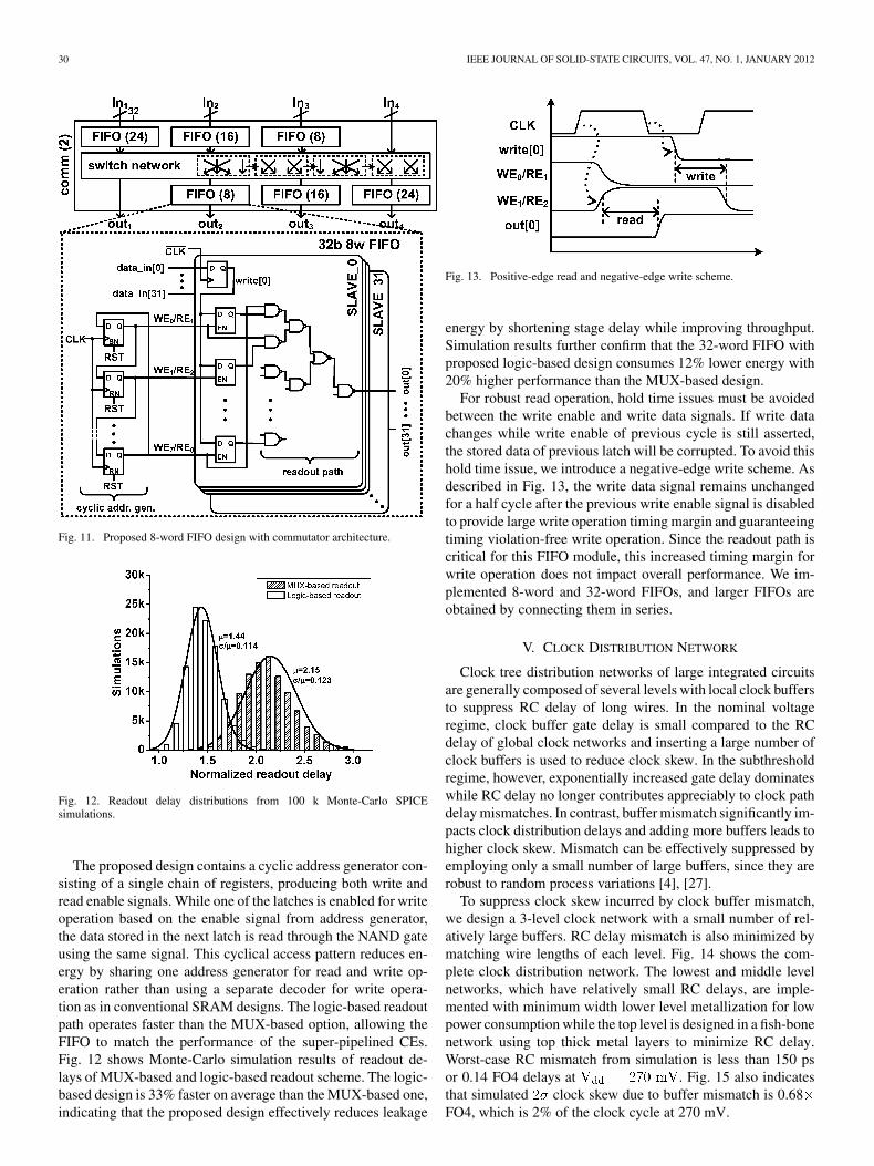
To mitigate these performance and variation issues, we pro-pose the use of a latch-based memory. Although latch-basedmemory as described in [5] increases read/write margins andoffers potential performance improvements, additional addressgenerator or decoder is necessary for read/write address signalgeneration. In addition, MUX-based readout paths are slow andsuffer from leakage energy overhead due to the correspond-ingly long cycle time. For improved energy efficiency, we pro-pose a latch-based memory with dedicated address generatorand logic-based readout path. The entire FIFO architecture isdescribed in Fig. 11.
30 IEEE JOURNAL OF SOLID-STATE CIRCUITS, VOL. 47, NO. 1, JANUARY 2012
Fig. 11. Proposed 8-word FIFO design with commutator architecture.
Fig. 12. Readout delay distributions from 100 k Monte-Carlo SPICEsimulations.
The proposed design contains a cyclic address generator con-sisting of a single chain of registers, producing both write andread enable signals. While one of the latches is enabled for writeoperation based on the enable signal from address generator,the data stored in the next latch is read through the NAND gateusing the same signal. This cyclical access pattern reduces en-ergy by sharing one address generator for read and write op-eration rather than using a separate decoder for write opera-tion as in conventional SRAM designs. The logic-based readoutpath operates faster than the MUX-based option, allowing theFIFO to match the performance of the super-pipelined CEs.Fig. 12 shows Monte-Carlo simulation results of readout de-lays of MUX-based and logic-based readout scheme. The logic-based design is 33% faster on average than the MUX-based one,indicating that the proposed design effectively reduces leakage
Fig. 13. Positive-edge read and negative-edge write scheme.
energy by shortening stage delay while improving throughput.Simulation results further confirm that the 32-word FIFO withproposed logic-based design consumes 12% lower energy with20% higher performance than the MUX-based design.
For robust read operation, hold time issues must be avoidedbetween the write enable and write data signals. If write datachanges while write enable of previous cycle is still asserted,the stored data of previous latch will be corrupted. To avoid thishold time issue, we introduce a negative-edge write scheme. Asdescribed in Fig. 13, the write data signal remains unchangedfor a half cycle after the previous write enable signal is disabledto provide large write operation timing margin and guaranteeingtiming violation-free write operation. Since the readout path iscritical for this FIFO module, this increased timing margin forwrite operation does not impact overall performance. We im-plemented 8-word and 32-word FIFOs, and larger FIFOs areobtained by connecting them in series.
V. CLOCK DISTRIBUTION NETWORK
Clock tree distribution networks of large integrated circuitsare generally composed of several levels with local clock buffersto suppress RC delay of long wires. In the nominal voltageregime, clock buffer gate delay is small compared to the RCdelay of global clock networks and inserting a large number ofclock buffers is used to reduce clock skew. In the subthresholdregime, however, exponentially increased gate delay dominateswhile RC delay no longer contributes appreciably to clock pathdelay mismatches. In contrast, buffer mismatch significantly im-pacts clock distribution delays and adding more buffers leads tohigher clock skew. Mismatch can be effectively suppressed byemploying only a small number of large buffers, since they arerobust to random process variations [4], [27].
To suppress clock skew incurred by clock buffer mismatch,we design a 3-level clock network with a small number of rel-atively large buffers. RC delay mismatch is also minimized bymatching wire lengths of each level. Fig. 14 shows the com-plete clock distribution network. The lowest and middle levelnetworks, which have relatively small RC delays, are imple-mented with minimum width lower level metallization for lowpower consumption while the top level is designed in a fish-bonenetwork using top thick metal layers to minimize RC delay.Worst-case RC mismatch from simulation is less than 150 psor 0.14 FO4 delays at . Fig. 15 also indicatesthat simulated clock skew due to buffer mismatch is 0.68FO4, which is 2% of the clock cycle at 270 mV.
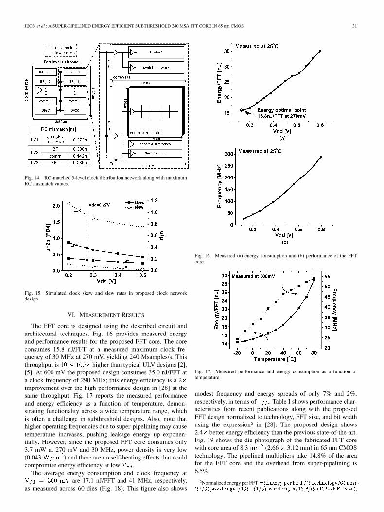
JEON et al.: A SUPER-PIPELINED ENERGY EFFICIENT SUBTHRESHOLD 240 MS/s FFT CORE IN 65 nm CMOS 31
Fig. 14. RC-matched 3-level clock distribution network along with maximumRC mismatch values.
Fig. 15. Simulated clock skew and slew rates in proposed clock networkdesign.
VI. MEASUREMENT RESULTS
The FFT core is designed using the described circuit andarchitectural techniques. Fig. 16 provides measured energyand performance results for the proposed FFT core. The coreconsumes 15.8 nJ/FFT at a measured maximum clock fre-quency of 30 MHz at 270 mV, yielding 240 Msamples/s. Thisthroughput is higher than typical ULV designs [2],[5]. At 600 mV the proposed design consumes 35.0 nJ/FFT ata clock frequency of 290 MHz; this energy efficiency is a 2improvement over the high performance design in [28] at thesame throughput. Fig. 17 reports the measured performanceand energy efficiency as a function of temperature, demon-strating functionality across a wide temperature range, whichis often a challenge in subthreshold designs. Also, note thathigher operating frequencies due to super-pipelining may causetemperature increases, pushing leakage energy up exponen-tially. However, since the proposed FFT core consumes only3.7 mW at 270 mV and 30 MHz, power density is very low(0.043 ) and there are no self-heating effects that couldcompromise energy efficiency at low .
The average energy consumption and clock frequency atare 17.1 nJ/FFT and 41 MHz, respectively,
as measured across 60 dies (Fig. 18). This figure also shows
Fig. 16. Measured (a) energy consumption and (b) performance of the FFTcore.
Fig. 17. Measured performance and energy consumption as a function oftemperature.
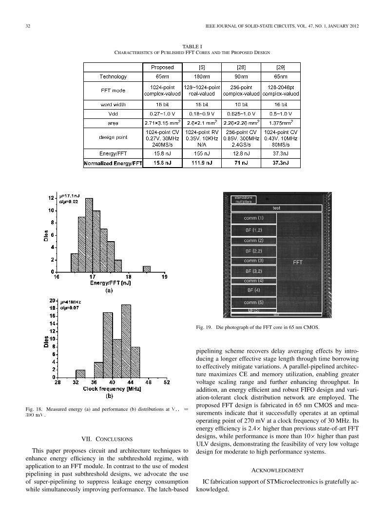
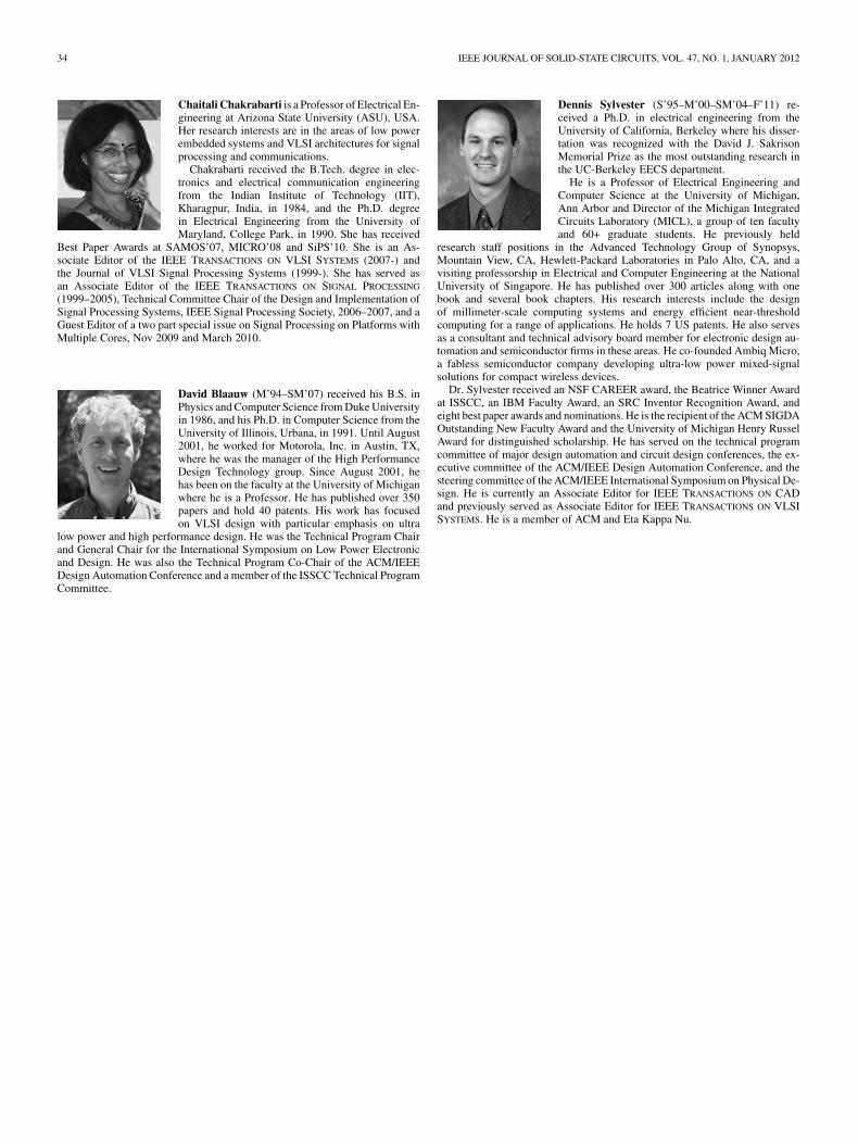
modest frequency and energy spreads of only 7% and 2%,respectively, in terms of . Table I shows performance char-acteristics from recent publications along with the proposedFFT design normalized to technology, FFT size, and bit widthusing the expression2 in [28]. The proposed design shows2.4 better energy efficiency than the previous state-of-the-art.Fig. 19 shows the die photograph of the fabricated FFT corewith core area of 8.3 (2.66 3.12 mm) in 65 nm CMOStechnology. The pipelined multipliers take 14.8% of the areafor the FFT core and the overhead from super-pipelining is6.5%.
2Normalized energy per FFT �������� ��������� ����������������������������� �������������������� ���� ����������� �����.
32 IEEE JOURNAL OF SOLID-STATE CIRCUITS, VOL. 47, NO. 1, JANUARY 2012
TABLE ICHARACTERISTICS OF PUBLISHED FFT CORES AND THE PROPOSED DESIGN
Fig. 18. Measured energy (a) and performance (b) distributions at � �
��� ��.
VII. CONCLUSIONS
This paper proposes circuit and architecture techniques toenhance energy efficiency in the subthreshold regime, withapplication to an FFT module. In contrast to the use of modestpipelining in past subthreshold designs, we advocate the useof super-pipelining to suppress leakage energy consumptionwhile simultaneously improving performance. The latch-based
Fig. 19. Die photograph of the FFT core in 65 nm CMOS.
pipelining scheme recovers delay averaging effects by intro-ducing a longer effective stage length through time borrowingto effectively mitigate variations. A parallel-pipelined architec-ture maximizes CE and memory utilization, enabling greatervoltage scaling range and further enhancing throughput. Inaddition, an energy efficient and robust FIFO design and vari-ation-tolerant clock distribution network are employed. Theproposed FFT design is fabricated in 65 nm CMOS and mea-surements indicate that it successfully operates at an optimaloperating point of 270 mV at a clock frequency of 30 MHz. Itsenergy efficiency is 2.4 higher than previous state-of-art FFTdesigns, while performance is more than 10 higher than pastULV designs, demonstrating the feasibility of very low voltagedesign for moderate to high performance systems.
ACKNOWLEDGMENT
IC fabrication support of STMicroelectronics is gratefully ac-knowledged.

JEON et al.: A SUPER-PIPELINED ENERGY EFFICIENT SUBTHRESHOLD 240 MS/s FFT CORE IN 65 nm CMOS 33
REFERENCES
[1] G. Chen, M. Fojtik, D. Kim, D. Fick, J. Park, M. Seok, M.-T. Chen, Z.Foo, D. Sylvester, and D. Blaauw, “Millimeter-scale nearly perpetualsensor system with stacked battery and solar cells,” in IEEE Int. Solid-State Circuits Conf. Dig. Tech. Papers, Feb. 2010, pp. 288–289.
[2] S. R. Sridhara, M. DiRenzo, S. Lingam, S.-J. Lee, R. Blazquez, J.Maxey, S. Ghanem, Y.-H. Lee, R. Abdallah, P. Singh, and M. Goel,“Microwatt embedded processor platform for medical system-on-chipapplications,” IEEE J. Solid-State Circuits, vol. 46, no. 4, pp. 721–730,Apr. 2011.
[3] B. Zhai, D. Blaauw, D. Sylvester, and K. Flautner, “Theoretical andpractical limits of dynamic voltage scaling,” in Proc. Design Automa-tion Conf., May 2005, pp. 868–873.
[4] B. Zhai, S. Hanson, D. Blaauw, and D. Sylvester, “Analysis and mit-igation of variability in subthreshold design,” in Proc. Int. Symp. LowPower Electronics and Design, Aug. 2005, pp. 20–25.
[5] A. Wang and A. Chandrakasan, “A 180-mV subthreshold FFT pro-cessor using a minimum energy design methodology,” IEEE J. Solid-State Circuits, vol. 40, no. 1, pp. 310–319, Jan. 2005.
[6] B. M. Baas, “A low-power, high-performance, 1024-point FFT pro-cessor,” IEEE J. Solid-State Circuits, vol. 34, no. 3, pp. 380–387, Mar.1999.
[7] M. Seok, D. Jeon, C. Chakrabarti, D. Blaauw, and D. Sylvester, “A 0.27V 30 MHz 17.7 nJ/transform 1024-pt complex FFT core with super-pipelining,” in IEEE Int. Solid-State Circuits Conf. Dig. Tech. Papers,Feb. 2011, pp. 342–343.
[8] V. Srinivasan, D. Brooks, M. Gschwind, P. Bose, V. Zyuban, P. N.Strenski, and P. G. Emma, “Optimizing pipelines for power and perfor-mance,” in Proc. Int. Symp. Microarchitecture, Nov. 2002, pp. 333–344.
[9] M. S. Hrishikesh, N. P. Jouppi, K. I. Farkas, D. Burger, S. W. Keckler,and P. Shivakumar, “The optimal logic depth per pipeline stage is 6to 8 FO4 inverter delays,” in Proc. Int. Symp. Computer Architecture,May 2002, pp. 14–24.
[10] A. Chandrakasan and R. Brodersen, Low-Power CMOS Design. NewYork: Wiley-IEEE Press, 1998.
[11] M. Seok, S. Hanson, Y.-S. Lin, Z. Foo, D. Kim, Y. Lee, N. Liu, D.Sylvester, and D. Blaauw, “The phoenix processor: A 30 pW platformfor sensor applications,” in Proc. IEEE Symp. VLSI Circuits, Jun. 2008,pp. 188–189.
[12] B. H. Calhoun, A. Wang, and A. Chandrakasan, “Modeling and sizingfor minimum energy operation in subthreshold circuits,” IEEE J. Solid-State Circuits, vol. 40, no. 9, pp. 1778–1786, Sep. 2005.
[13] S. Hanson, B. Zhai, M. Seok, B. Cline, K. Zhou, M. Singhal, M.Minuth, J. Olson, L. Nazhandali, T. Austin, D. Sylvester, and D.Blaauw, “Performance and variability optimization strategies in asub-200 mV, 3.5 pJ/inst, 11 nW subthreshold processor,” in Proc.IEEE Symp. VLSI Circuits, Jun. 2007, pp. 152–153.
[14] D. Harris, Skew-Tolerant Circuit Design. Burlington: Morgan Kauf-mann, 2000.
[15] M. Wieckowski, Y. M. Park, C. Tokunaga, D. W. Kim, Z. Foo, D.Sylvester, and D. Blaauw, “Timing yield enhancement through softedge flip-flop based design,” in Proc. IEEE Custom Integrated CircuitsConf., Sep. 2008, pp. 543–546.
[16] H. Ando, Y. Yoshida, A. Inoue, I. Sugiyama, T. Asakawa, K. Morita,T. Muta, T. Motokurumada, S. Okada, H. Yamashita, Y. Satsukawa, A.Konmoto, R. Yamashita, and H. Sugiyama, “A 1.3-GHz fifth-genera-tion SPARC64 microprocessor,” IEEE J. Solid-State Circuits, vol. 38,no. 11, pp. 1896–1905, Nov. 2003.
[17] S. He and M. Torkelson, “A new approach to pipeline FFT processor,”in Proc. Int. Parallel Processing Symp., Apr. 1996, pp. 766–770.
[18] W. Tang and L. Wang, “Cooperative OFDM for energy efficient wire-less sensor networks,” in Proc. IEEE Workshop on Signal ProcessingSystems, Oct. 2008, pp. 77–82.
[19] D. Zhao, H. Ma, and L. Liu, “Event classification for living environ-ment surveillance using audio sensor networks,” in Proc. IEEE Int.Conf. Multimedia and Expo, Jul. 2010, pp. 528–533.
[20] E. E. Swartzlander, W. K. W. Young, and S. J. Joseph, “A radix 4delay commutator for fast Fourier transform processor implementa-tion,” IEEE J. Solid-State Circuits, vol. 19, no. 5, pp. 702–709, Oct.1984.
[21] T. Gemmeke, M. Gansen, H. J. Stockmanns, and T. G. Noll, “Designoptimization of low-power high-performance DSP building blocks,”IEEE J. Solid-State Circuits, vol. 39, no. 7, pp. 1131–1139, Jul. 2004.
[22] S. Yoshizawa, K. Nishi, and Y. Miyanaga, “Reconfigurable two-dimen-sional pipeline FFT processor in OFDM cognitive radio systems,” inProc. IEEE Int. Symp. Circuits and Systems, May 2008, pp. 1248–1251.
[23] C.-C. Wang, J.-M. Huang, and H.-C. Cheng, “A 2 K/8 K mode small-area FFT processor for OFDM demodulation of DVB-T receivers,”IEEE Trans. Consumer Electronics, vol. 51, no. 1, pp. 28–32, Feb.2005.
[24] B. H. Calhoun and A. P. Chandrakasan, “A 256-kb 65-nmsub-threshold SRAM design for ultra-low-voltage operation,” IEEE J.Solid-State Circuits, vol. 42, no. 3, pp. 680–688, Mar. 2007.
[25] C.-H. Lo and S.-Y. Huang, “P-P-N based 10T SRAM cell for low-leakage and resilient subthreshold operation,” IEEE J. Solid-State Cir-cuits, vol. 46, no. 3, pp. 520–529, Mar. 2011.
[26] M.-F. Chang, S.-W. Chang, P.-W. Chou, and W.-C. Wu, “A 130 mVSRAM with expanded write and read margins for subthreshold appli-cations,” IEEE J. Solid-State Circuits, vol. 46, no. 2, pp. 520–529, Feb.2011.
[27] M. Seok, D. Blaauw, and D. Sylvester, “Clock network design forultra-low power applications,” in Proc. Int. Symp. Low Power Elec-tronics and Design, Aug. 2010, pp. 271–276.
[28] Y. Chen, Y.-W. Lin, Y.-C. Tsao, and C.-Y. Lee, “A 2.4-Gsample/sDVFS FFT processor for MIMO OFDM communication systems,”IEEE J. Solid-State Circuits, vol. 43, no. 5, pp. 1260–1273, May2008.
[29] C.-H. Yang, T.-H. Yu, and D. Markovic, “A 5.8 mW 3GPP-LTE com-pliant 8 � 8 MIMO sphere decoder chip with soft-outputs,” in Proc.IEEE Symp. VLSI Circuits, Jun. 2010, pp. 209–210.
Dongsuk Jeon (S’10) received a B.S degree in elec-trical engineering from the Seoul National Univer-sity, South Korea, in 2009. He is currently pursuinga Ph.D. in electrical engineering at the University ofMichigan, Ann Arbor.
His research interests include energy efficientsignal processing, subthreshold circuit design anderror-resilient systems.
Mr. Jeon is the recipient of the Samsung Scholar-ship for graduate student.
Mingoo Seok (S’05) received the Bachelor degree(summa cum laude) in electrical engineering fromSeoul National University, South Korea, in 2005, andthe Master degree and PhD degree from Universityof Michigan in 2007 and 2011, respectively, all inelectrical engineering. He is currently a member oftechnical staff in the Systems and Applications R&DCenter of Texas Instruments, Dallas Texas. He willjoin the EE department of Columbia University inNov 2011 as an assistant professor.
He has published more than 25 journal and confer-ence papers in his field of research, which includes low power circuit and systemdesign methodologies for improving energy efficiency, performance, and vari-ability both in digital and analog domains. Dr. Seok received 1998–2001 Excel-lency Fellowship from Seoul National University, 1999 Distinguished Under-graduate Scholarship from the Korea Foundation for Advanced Studies, 2005Doctoral Fellowship from the same organization, and 2008 Rackham Pre-Doc-toral Fellowship from University of Michigan, Ann Arbor. He also won 2009AMD/CICC Student Scholarship Award for picowatt voltage reference workand 2009 DAC/ISSCC Student Design Contest for the 35 pW sensor platformdesign (also known as Phoenix Processor). He holds one pending US patent andseveral invention disclosures.
34 IEEE JOURNAL OF SOLID-STATE CIRCUITS, VOL. 47, NO. 1, JANUARY 2012
Chaitali Chakrabarti is a Professor of Electrical En-gineering at Arizona State University (ASU), USA.Her research interests are in the areas of low powerembedded systems and VLSI architectures for signalprocessing and communications.
Chakrabarti received the B.Tech. degree in elec-tronics and electrical communication engineeringfrom the Indian Institute of Technology (IIT),Kharagpur, India, in 1984, and the Ph.D. degreein Electrical Engineering from the University ofMaryland, College Park, in 1990. She has received
Best Paper Awards at SAMOS’07, MICRO’08 and SiPS’10. She is an As-sociate Editor of the IEEE TRANSACTIONS ON VLSI SYSTEMS (2007-) andthe Journal of VLSI Signal Processing Systems (1999-). She has served asan Associate Editor of the IEEE TRANSACTIONS ON SIGNAL PROCESSING
(1999–2005), Technical Committee Chair of the Design and Implementation ofSignal Processing Systems, IEEE Signal Processing Society, 2006–2007, and aGuest Editor of a two part special issue on Signal Processing on Platforms withMultiple Cores, Nov 2009 and March 2010.
David Blaauw (M’94–SM’07) received his B.S. inPhysics and Computer Science from Duke Universityin 1986, and his Ph.D. in Computer Science from theUniversity of Illinois, Urbana, in 1991. Until August2001, he worked for Motorola, Inc. in Austin, TX,where he was the manager of the High PerformanceDesign Technology group. Since August 2001, hehas been on the faculty at the University of Michiganwhere he is a Professor. He has published over 350papers and hold 40 patents. His work has focusedon VLSI design with particular emphasis on ultra
low power and high performance design. He was the Technical Program Chairand General Chair for the International Symposium on Low Power Electronicand Design. He was also the Technical Program Co-Chair of the ACM/IEEEDesign Automation Conference and a member of the ISSCC Technical ProgramCommittee.
Dennis Sylvester (S’95–M’00–SM’04–F’11) re-ceived a Ph.D. in electrical engineering from theUniversity of California, Berkeley where his disser-tation was recognized with the David J. SakrisonMemorial Prize as the most outstanding research inthe UC-Berkeley EECS department.
He is a Professor of Electrical Engineering andComputer Science at the University of Michigan,Ann Arbor and Director of the Michigan IntegratedCircuits Laboratory (MICL), a group of ten facultyand 60+ graduate students. He previously held
research staff positions in the Advanced Technology Group of Synopsys,Mountain View, CA, Hewlett-Packard Laboratories in Palo Alto, CA, and avisiting professorship in Electrical and Computer Engineering at the NationalUniversity of Singapore. He has published over 300 articles along with onebook and several book chapters. His research interests include the designof millimeter-scale computing systems and energy efficient near-thresholdcomputing for a range of applications. He holds 7 US patents. He also servesas a consultant and technical advisory board member for electronic design au-tomation and semiconductor firms in these areas. He co-founded Ambiq Micro,a fabless semiconductor company developing ultra-low power mixed-signalsolutions for compact wireless devices.
Dr. Sylvester received an NSF CAREER award, the Beatrice Winner Awardat ISSCC, an IBM Faculty Award, an SRC Inventor Recognition Award, andeight best paper awards and nominations. He is the recipient of the ACM SIGDAOutstanding New Faculty Award and the University of Michigan Henry RusselAward for distinguished scholarship. He has served on the technical programcommittee of major design automation and circuit design conferences, the ex-ecutive committee of the ACM/IEEE Design Automation Conference, and thesteering committee of the ACM/IEEE International Symposium on Physical De-sign. He is currently an Associate Editor for IEEE TRANSACTIONS ON CADand previously served as Associate Editor for IEEE TRANSACTIONS ON VLSISYSTEMS. He is a member of ACM and Eta Kappa Nu.