Embed Size (px)
Citation preview
A STUDY ON A LOW PHASE NOISE CHARGE PUMP PHASE-LOCKEDLOOP AT 2.8 GHZ
A THESIS SUBMITTED TOTHE GRADUATE SCHOOL OF NATURAL AND APPLIED SCIENCES
OFMIDDLE EAST TECHNICAL UNIVERSITY
BY
MAHSA KEYKHALI
IN PARTIAL FULFILLMENT OF THE REQUIREMENTSFOR
THE DEGREE OF MASTER OF SCIENCEIN
ELECTRICAL AND ELECTRONICS ENGINEERING
FEBRUARY 2016

Approval of the thesis:
A STUDY ON A LOW PHASE NOISE CHARGE PUMP PHASE-LOCKEDLOOP AT 2.8 GHZ
submitted by MAHSA KEYKHALI in partial fulfillment of the requirements for thedegree of Master of Science in Electrical and Electronics Engineering Depart-ment, Middle East Technical University by,
Prof. Dr. Gülbin Dural ÜnverDean, Graduate School of Natural and Applied Sciences
Prof. Dr. Gönül Turhan SayanHead of Department, Electrical and Electronics Engineering
Prof. Dr. Nevzat Güneri GençerSupervisor, Elec. and Electronics Eng. Dept., METU
Examining Committee Members:
Prof. Dr. Cengiz BesikçiElectrical and Electronics Engineering Dept., METU
Prof. Dr. Nevzat Güneri GençerElectrical and Electronics Engineering Dept., METU
Prof. Dr. Tayfun AkınElectrical and Electronics Engineering Dept., METU
Prof. Dr. Haluk KülahElectrical and Electronics Engineering Dept., METU
Assoc. Prof. Dr. Arif Sanlı ErgünElec. and Electronics Engineering Dept., ETU
Date:
I hereby declare that all information in this document has been obtained andpresented in accordance with academic rules and ethical conduct. I also declarethat, as required by these rules and conduct, I have fully cited and referenced allmaterial and results that are not original to this work.
Name, Last Name: MAHSA KEYKHALI
Signature :
iv
ABSTRACT
A STUDY ON A LOW PHASE NOISE CHARGE PUMP PHASE-LOCKEDLOOP AT 2.8 GHZ
Keykhali, Mahsa
M.S., Department of Electrical and Electronics Engineering
Supervisor : Prof. Dr. Nevzat Güneri Gençer
February 2016, 92 pages
Today, the most challenging problem that Phase Locked Loop (PLL) designers facewith is the design of ultra-low phase noise PLL at high frequencies. In this research,a high frequency charge-pump phase-locked loop (CPPLL) with low phase noise isstudied. At the beginning stage, a gate grounding Colpitts Voltage Controlled Os-cillator (VCO) using a High Electron Mobility Transistor (HEMT) is designed. Theprovided VCO achieved -131dBc/Hz at 1 MHz offset phase noise with the 2.6-3 GHzoscillating frequency ranges. Inserting a PLL chip around the VCO can reduce theachieved phase noise. Therefore, to investigate this phenomenon a CPPLL is simu-lated. The CPPLL components, namely the Phase Frequency Detector (PFD), ChargePump (CP), and the frequency divider are investigated individually. The loop filterdesign is also taken into account as it plays a vital role in determining the loop band-width of the CPPLL. Finally, the phase noise of the implemented CPPLL is simulated.Assuming noiseless crystal oscillator, the phase noise is calculated as -120 dBc/Hzat 100 Hz offset. The phase noise is decreased successfully 90 dBc compared to theVCO phase noise (-32 dBc/Hz at 100 Hz). When the noise of the crystal oscillator isincluded, the phase noise at 100 Hz reached to -101 dBc/Hz. Related simulations areconducted on microwave simulation tool (ADS).
v
Keywords: PLL, phase noise, CPPLL, VCO, HEMT, ADS, PFD, CP
vi
ÖZ
2.8 GHZ’DE DÜSÜK FAZ GÜRÜLTÜLÜ YÜK POMPALI FAZ KILITLEMELIDÖNGÜ ÜZERINE BIR ÇALISMA
Keykhali, Mahsa
Yüksek Lisans, Elektrik ve Elektronik Mühendisligi Bölümü
Tez Yöneticisi : Prof. Dr. Nevzat Güneri Gençer
Subat 2016 , 92 sayfa
Günümüzde; faz kilitlemeli döngü (PLL) tasarımlarıyla ugrasan arastırmacıların kar-sılastıgı en zor problem, yüksek frekansta çalısan, düsük faz gürültüsüne sahip olanPLL tasarımları yapmaktır. Bu çalısmada, yüksek frekansta çalısan düsük faz gürül-tülü yük pompalı faz kilitlemeli döngü (CPPLL) tasarımı yapılmıstır. Ilk bölümde,yüksek hareketli electron transistörler (HEMT) kullanılarak, topraklanmıs kapılı Col-pitts voltaj kontrollü osilatör (VCO) tasarlanmıstır. Tasarlanan VCO 2.6-3 GHz fre-kans aralıgında çalısmakta olup, faz gürültüsü 1 MHz’de -131 dBc/Hz’dir. Voltajkontrollü osilatörün çevresine PLL çip yerlestirilerek faz gürültüsü azaltılabilir. Budurumu gözlemlemek amacıyla CPPLL benzetim çalısmaları yapılmıstır. CPPLL ta-sarımı yapılırken; Faz Frekansı Detektörü (PFD), Yük Pompası (CP) ve frekans bö-lücüler ayrı ayrı incelenmistir. Ayrıca, CPPLL’in döngü bant genisliginin belirlenme-sinde önemli bir rol oynadıgı için döngü filtre tasarımı da dikkate alınmıstır. Son ola-rak, CPPLL’in faz gürültüsü için benzetim çalısmaları yapılmıstır. Gürültüsüz kristalosilatör varsayılarak, faz gürültüsü 100 Hz’de -120 dBc/Hz olarak bulunmustur. Fazgürültüsü, voltaj kontrollü osilatörün faz gürültüsüne (100 Hz de -32 dBc/Hz) göre90 dBc azaltılmıstır. Kristal osilatörün gürültüsü eklendiginde ise, 100 Hz’deki fazgürültüsü -101 dBc/Hz’e ulasmıstır. Ilgili benzetim çalısmaları, mikrodalga benzetimaracı ADS ile yapılmıstır.
vii
Anahtar Kelimeler: PLL, Faz Gürültüsü, CPPLL, VCO, HEMT, ADS, PFD, CP
viii
Dedicated to,
my husband Nasser for his love and support,
my mother who was always there for me,
the memory of my father, I wish he were alive.
ix
ACKNOWLEDGMENTS
The author would like to express her sincere appreciation to her supervisor, Prof. Dr.Nevzat Güneri GENÇER for his support, valuable guidance, supervision and friendlyencouragement.
The author is grateful to Dr. Fatih Koçer and Dr. Bortecene Terlemez for their supportand advices.
The author would like to express her sincere gratings and appreciations to Dr. AminRonaghzadeh for his support and valuable advices. This work would not have beenpossible without his immediate support and practical ideas in desperate situations.
The author would like to extend her deepest gratitude to Azadeh Kamali Tafreshi forher support and friendship.
The author would also like to acknowledge her gratitude to her friends and lab matesDr. Reyhan Zengin, Damla Alptekin, Keivan Kaboutari, Elyar Ghalichi, CaglayanDurlu and Öykü Çobanoglu and her lovely friend Cansu Akbay for their friendship,support and advices.
For translating the idea to experimental studies, author would like to express hergratitude to the Scientific and Technological Research Council of Turkey (TUBITAK)for supporting the experimental work financially with project code 114E036.
The author would like to express her most sincere gratitude to her grandmother whohas always supported and encouraged her to do her best in all matters of life.
The author would like to express a deep sense of gratitude to my parents, especiallyto my dearest darling mom, who has always stood by me like a pillar in times of needand to whom I owe my life for her constant love, encouragement, moral support andblessings. Special thanks are due to my one and only loving brother Mohsen whoalways strengthened my morale by standing by me in all situations.
The author would also like to express her heartfelt gratitude to memory of her fatherfor his endless love, support and patience during her life.
Finally, the author feels grateful to her husband Nasser for his patience and under-standing. His encouragement, support and endless love have always been the greatestassets of her life.
x
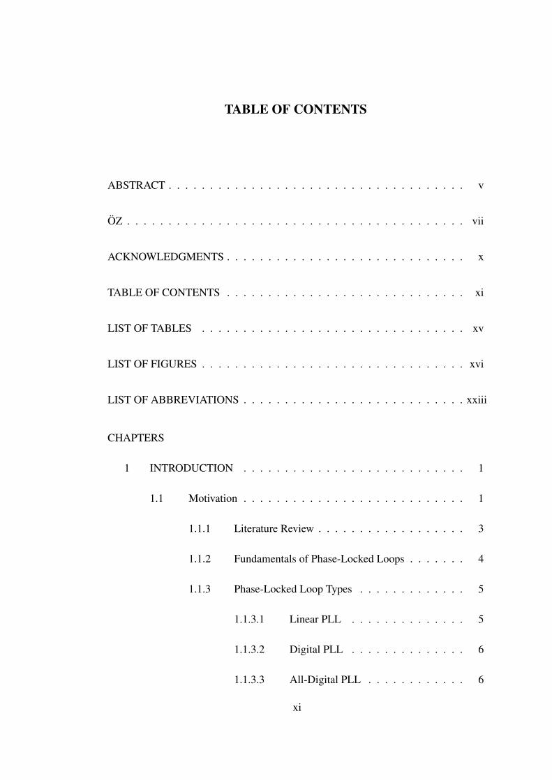
TABLE OF CONTENTS
ABSTRACT . . . . . . . . . . . . . . . . . . . . . . . . . . . . . . . . . . . . v
ÖZ . . . . . . . . . . . . . . . . . . . . . . . . . . . . . . . . . . . . . . . . . vii
ACKNOWLEDGMENTS . . . . . . . . . . . . . . . . . . . . . . . . . . . . . x
TABLE OF CONTENTS . . . . . . . . . . . . . . . . . . . . . . . . . . . . . xi
LIST OF TABLES . . . . . . . . . . . . . . . . . . . . . . . . . . . . . . . . xv
LIST OF FIGURES . . . . . . . . . . . . . . . . . . . . . . . . . . . . . . . . xvi
LIST OF ABBREVIATIONS . . . . . . . . . . . . . . . . . . . . . . . . . . . xxiii
CHAPTERS
1 INTRODUCTION . . . . . . . . . . . . . . . . . . . . . . . . . . . 1
1.1 Motivation . . . . . . . . . . . . . . . . . . . . . . . . . . . 1
1.1.1 Literature Review . . . . . . . . . . . . . . . . . . 3
1.1.2 Fundamentals of Phase-Locked Loops . . . . . . . 4
1.1.3 Phase-Locked Loop Types . . . . . . . . . . . . . 5
1.1.3.1 Linear PLL . . . . . . . . . . . . . . 5
1.1.3.2 Digital PLL . . . . . . . . . . . . . . 6
1.1.3.3 All-Digital PLL . . . . . . . . . . . . 6
xi
1.1.3.4 Charge Pump PLL . . . . . . . . . . . 8
1.2 Scope of this thesis . . . . . . . . . . . . . . . . . . . . . . 10
1.3 Thesis Organization . . . . . . . . . . . . . . . . . . . . . . 11
2 PHASE-LOCKED LOOPS . . . . . . . . . . . . . . . . . . . . . . . 13
2.1 Basic concepts . . . . . . . . . . . . . . . . . . . . . . . . . 13
2.1.1 Voltage Controlled Oscillator . . . . . . . . . . . . 13
2.1.2 Phase Detector . . . . . . . . . . . . . . . . . . . 14
2.2 Phase-Locked Loop . . . . . . . . . . . . . . . . . . . . . . 14
2.2.1 Basic structure . . . . . . . . . . . . . . . . . . . 14
2.2.2 Loop dynamics . . . . . . . . . . . . . . . . . . . 15
2.3 Charge pump PLL . . . . . . . . . . . . . . . . . . . . . . . 17
2.4 PLL components . . . . . . . . . . . . . . . . . . . . . . . . 17
2.4.1 Voltage Controlled Oscillator . . . . . . . . . . . . 17
2.4.1.1 General Considerations . . . . . . . . 18
2.4.1.2 Basic LC Oscillator Topologies . . . . 19
2.4.1.3 Voltage-Controlled Oscillators . . . . 19
2.4.2 Phase frequency detector . . . . . . . . . . . . . . 21
2.4.2.1 Basic PFD . . . . . . . . . . . . . . . 21
2.4.2.2 Pass-transistor DFF PFD . . . . . . . 22
2.4.3 Charge pump and loop filter . . . . . . . . . . . . 24
2.4.3.1 Single-Ended Charge Pumps . . . . . 25
xii
2.4.3.2 Loop Filter . . . . . . . . . . . . . . . 26
2.4.4 Frequency divider . . . . . . . . . . . . . . . . . . 27
2.4.4.1 CMOS D-FF . . . . . . . . . . . . . . 27
3 PLL BLOCKS DESIGN AND ANALYSIS . . . . . . . . . . . . . . 29
3.1 The VCO design proposed in this thesis study . . . . . . . . 29
3.1.1 HEMT transistor . . . . . . . . . . . . . . . . . . 30
3.1.2 Varactor . . . . . . . . . . . . . . . . . . . . . . . 35
3.2 The Frequency divider design proposed in this thesis study . 39
3.3 The PFD design proposed in this thesis study . . . . . . . . . 48
3.3.1 Basic PFD . . . . . . . . . . . . . . . . . . . . . . 49
3.3.2 CMOS PFD . . . . . . . . . . . . . . . . . . . . . 50
3.4 The Charge pump and loop filter design proposed in this the-sis study . . . . . . . . . . . . . . . . . . . . . . . . . . . . 53
3.4.1 Charge pump design summary . . . . . . . . . . . 55
4 SIMULATION RESULTS FOR IMPLEMENTED PLLS . . . . . . . 59
4.1 Analog-Digital PLL . . . . . . . . . . . . . . . . . . . . . . 59
4.2 All Analog PLL . . . . . . . . . . . . . . . . . . . . . . . . 64
4.3 Discussion . . . . . . . . . . . . . . . . . . . . . . . . . . . 66
5 PLL PHASE NOISE ANALYSIS . . . . . . . . . . . . . . . . . . . . 69
5.1 PLL Noise Analysis . . . . . . . . . . . . . . . . . . . . . . 69
5.2 PLL Noise Modeling and Simulation . . . . . . . . . . . . . 70
5.2.1 VCO noise analysis . . . . . . . . . . . . . . . . . 72
xiii
5.2.2 PFD and CP noise analysis . . . . . . . . . . . . . 73
5.2.3 Frequency divider noise analysis . . . . . . . . . . 76
5.2.4 CPPLL noise analysis . . . . . . . . . . . . . . . 78
6 CONCLUSION AND FUTURE WORK . . . . . . . . . . . . . . . . 85
REFERENCES . . . . . . . . . . . . . . . . . . . . . . . . . . . . . . . . . . 89
xiv

LIST OF TABLES
TABLES
Table 1.1 Characteristics of recent PLL circuits in the literature. . . . . . . . . 3
Table 1.2 PLL classification . . . . . . . . . . . . . . . . . . . . . . . . . . . 5
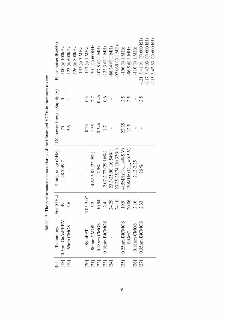
Table 1.3 The performance characteristics of the illustrated VCOs in literaturereview . . . . . . . . . . . . . . . . . . . . . . . . . . . . . . . . . . . . 9
Table 5.1 PLL closed loop parameters. the reference frequency (fref ), thedivider ratio (N), the natural frequency (ωn), the loop filter components(CP , RP and C2). . . . . . . . . . . . . . . . . . . . . . . . . . . . . . . 71
xv
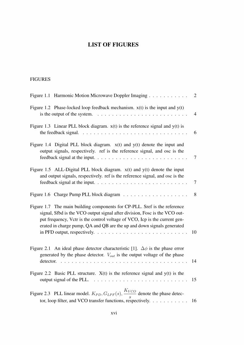
LIST OF FIGURES
FIGURES
Figure 1.1 Harmonic Motion Microwave Doppler Imaging . . . . . . . . . . . 2
Figure 1.2 Phase-locked loop feedback mechanism. x(t) is the input and y(t)is the output of the system. . . . . . . . . . . . . . . . . . . . . . . . . . 4
Figure 1.3 Linear PLL block diagram. x(t) is the reference signal and y(t) isthe feedback signal. . . . . . . . . . . . . . . . . . . . . . . . . . . . . . 6
Figure 1.4 Digital PLL block diagram. x(t) and y(t) denote the input andoutput signals, respectively. ref is the reference signal, and osc is thefeedback signal at the input. . . . . . . . . . . . . . . . . . . . . . . . . . 7
Figure 1.5 ALL-Digital PLL block diagram. x(t) and y(t) denote the inputand output signals, respectively. ref is the reference signal, and osc is thefeedback signal at the input. . . . . . . . . . . . . . . . . . . . . . . . . . 7
Figure 1.6 Charge Pump PLL block diagram . . . . . . . . . . . . . . . . . . 8
Figure 1.7 The main building components for CP-PLL. Sref is the referencesignal, Sfbd is the VCO output signal after division, Fosc is the VCO out-put frequency, Vctr is the control voltage of VCO, Icp is the current gen-erated in charge pump, QA and QB are the up and down signals generatedin PFD output, respectively. . . . . . . . . . . . . . . . . . . . . . . . . . 10
Figure 2.1 An ideal phase detector characteristic [1]. ∆φ is the phase errorgenerated by the phase detector. Vout is the output voltage of the phasedetector. . . . . . . . . . . . . . . . . . . . . . . . . . . . . . . . . . . . 14
Figure 2.2 Basic PLL structure. X(t) is the reference signal and y(t) is theoutput signal of the PLL. . . . . . . . . . . . . . . . . . . . . . . . . . . 15
Figure 2.3 PLL linear model. KPD, GLPF (s),KV CO
sdenote the phase detec-
tor, loop filter, and VCO transfer functions, respectively. . . . . . . . . . . 16
xvi
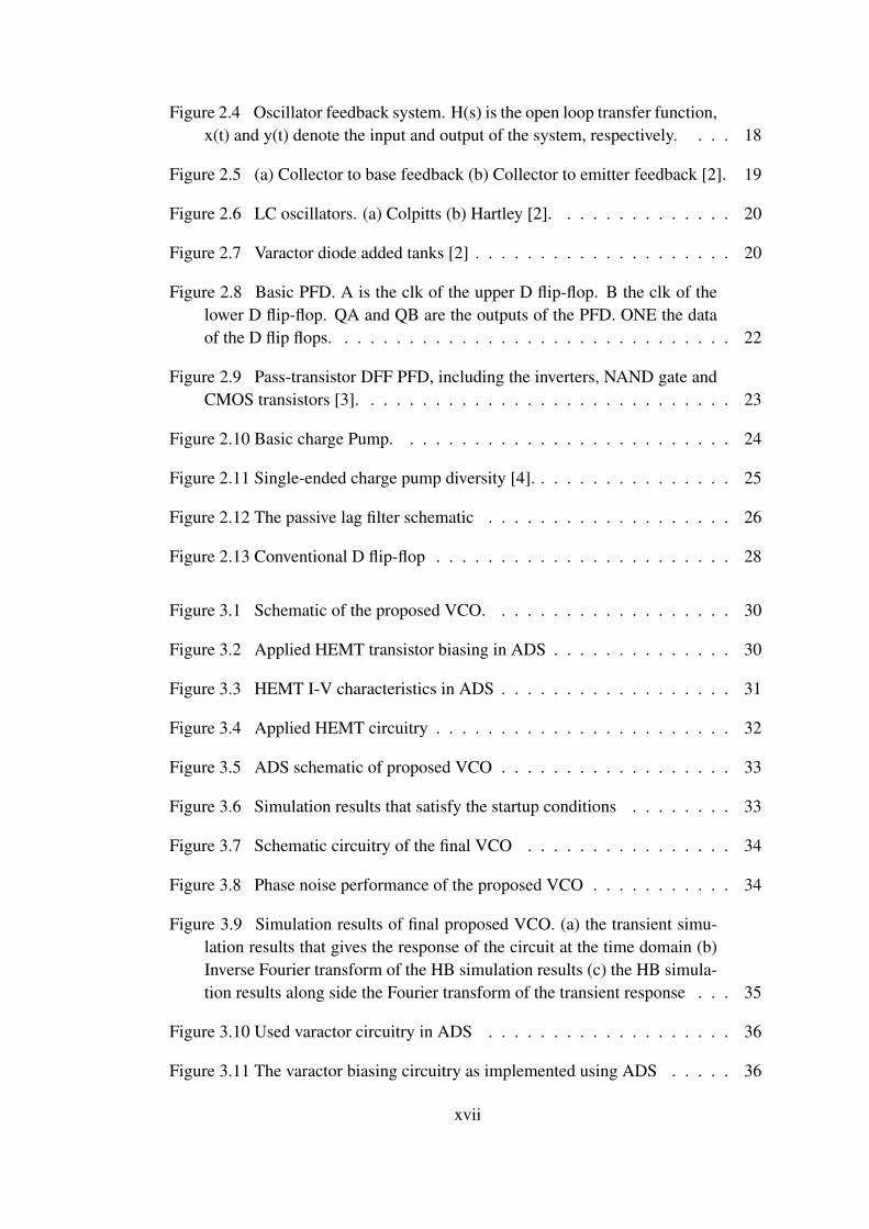
Figure 2.4 Oscillator feedback system. H(s) is the open loop transfer function,x(t) and y(t) denote the input and output of the system, respectively. . . . 18
Figure 2.5 (a) Collector to base feedback (b) Collector to emitter feedback [2]. 19
Figure 2.6 LC oscillators. (a) Colpitts (b) Hartley [2]. . . . . . . . . . . . . . 20
Figure 2.7 Varactor diode added tanks [2] . . . . . . . . . . . . . . . . . . . . 20
Figure 2.8 Basic PFD. A is the clk of the upper D flip-flop. B the clk of thelower D flip-flop. QA and QB are the outputs of the PFD. ONE the dataof the D flip flops. . . . . . . . . . . . . . . . . . . . . . . . . . . . . . . 22
Figure 2.9 Pass-transistor DFF PFD, including the inverters, NAND gate andCMOS transistors [3]. . . . . . . . . . . . . . . . . . . . . . . . . . . . . 23
Figure 2.10 Basic charge Pump. . . . . . . . . . . . . . . . . . . . . . . . . . 24
Figure 2.11 Single-ended charge pump diversity [4]. . . . . . . . . . . . . . . . 25
Figure 2.12 The passive lag filter schematic . . . . . . . . . . . . . . . . . . . 26
Figure 2.13 Conventional D flip-flop . . . . . . . . . . . . . . . . . . . . . . . 28
Figure 3.1 Schematic of the proposed VCO. . . . . . . . . . . . . . . . . . . 30
Figure 3.2 Applied HEMT transistor biasing in ADS . . . . . . . . . . . . . . 30
Figure 3.3 HEMT I-V characteristics in ADS . . . . . . . . . . . . . . . . . . 31
Figure 3.4 Applied HEMT circuitry . . . . . . . . . . . . . . . . . . . . . . . 32
Figure 3.5 ADS schematic of proposed VCO . . . . . . . . . . . . . . . . . . 33
Figure 3.6 Simulation results that satisfy the startup conditions . . . . . . . . 33
Figure 3.7 Schematic circuitry of the final VCO . . . . . . . . . . . . . . . . 34
Figure 3.8 Phase noise performance of the proposed VCO . . . . . . . . . . . 34
Figure 3.9 Simulation results of final proposed VCO. (a) the transient simu-lation results that gives the response of the circuit at the time domain (b)Inverse Fourier transform of the HB simulation results (c) the HB simula-tion results along side the Fourier transform of the transient response . . . 35
Figure 3.10 Used varactor circuitry in ADS . . . . . . . . . . . . . . . . . . . 36
Figure 3.11 The varactor biasing circuitry as implemented using ADS . . . . . 36
xvii
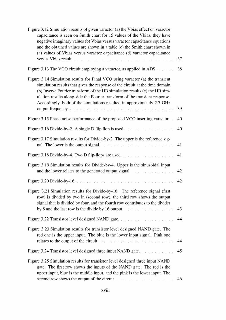
Figure 3.12 Simulation results of given varactor (a) the Vbias effect on varactorcapacitance is seen on Smith chart for 15 values of the Vbias, they havenegative imaginary values (b) Vbias versus varactor capacitance equationsand the obtained values are shown in a table (c) the Smith chart shown in(a) values of Vbias versus varactor capacitance (d) varactor capacitanceversus Vbias result . . . . . . . . . . . . . . . . . . . . . . . . . . . . . . 37
Figure 3.13 The VCO circuit employing a varactor, as applied in ADS. . . . . . 38
Figure 3.14 Simulation results for Final VCO using varactor (a) the transientsimulation results that gives the response of the circuit at the time domain(b) Inverse Fourier transform of the HB simulation results (c) the HB sim-ulation results along side the Fourier transform of the transient response.Accordingly, both of the simulations resulted in approximately 2.7 GHzoutput frequency . . . . . . . . . . . . . . . . . . . . . . . . . . . . . . . 39
Figure 3.15 Phase noise performance of the proposed VCO inserting varactor. . 40
Figure 3.16 Divide-by-2. A single D flip flop is used. . . . . . . . . . . . . . . 40
Figure 3.17 Simulation results for Divide-by-2. The upper is the reference sig-nal. The lower is the output signal. . . . . . . . . . . . . . . . . . . . . . 41
Figure 3.18 Divide-by-4. Two D flip-flops are used. . . . . . . . . . . . . . . . 41
Figure 3.19 Simulation results for Divide-by-4. Upper is the sinusoidal inputand the lower relates to the generated output signal. . . . . . . . . . . . . 42
Figure 3.20 Divide-by-16. . . . . . . . . . . . . . . . . . . . . . . . . . . . . . 42
Figure 3.21 Simulation results for Divide-by-16. The reference signal (firstrow) is divided by two in (second row), the third row shows the outputsignal that is divided by four, and the fourth row contributes to the dividerby 8 and the last row is the divide by 16 output. . . . . . . . . . . . . . . 43
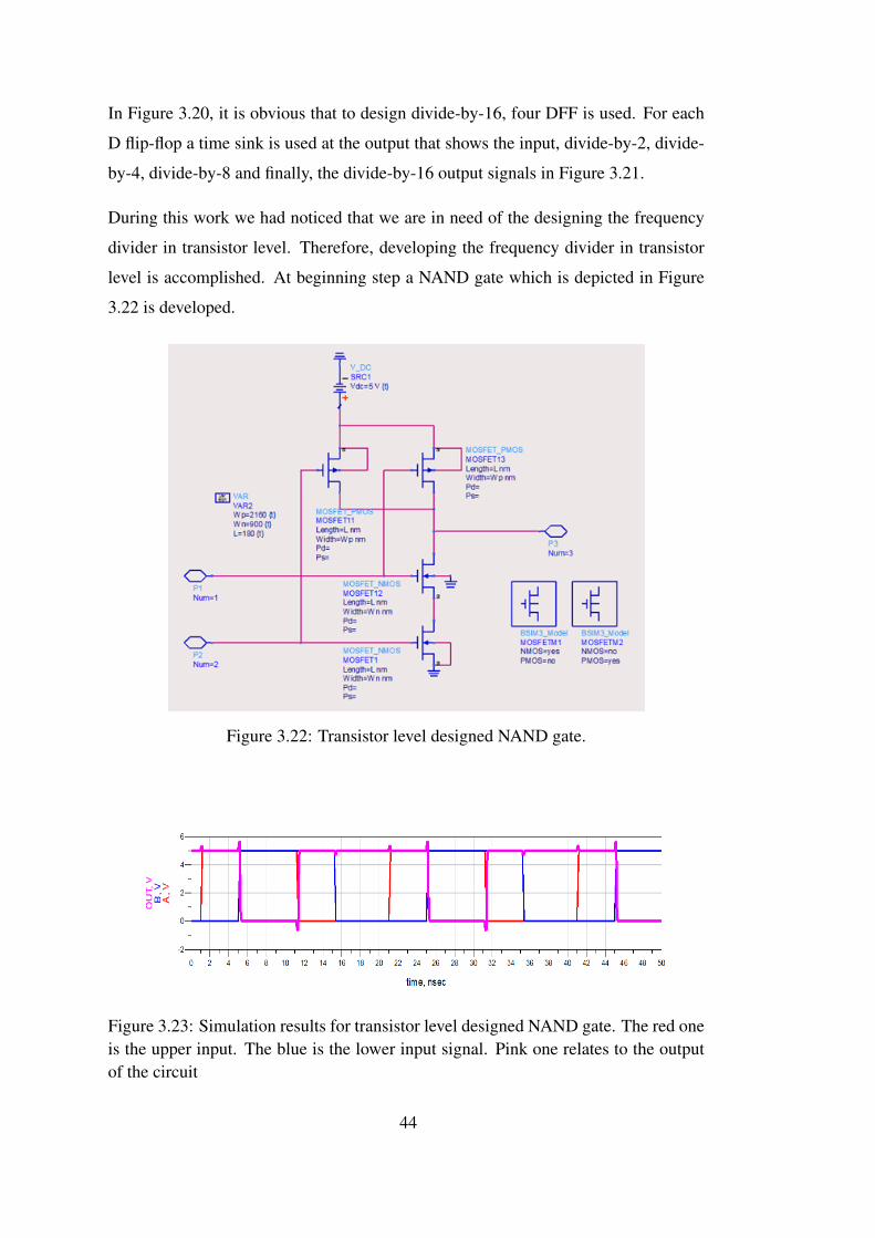
Figure 3.22 Transistor level designed NAND gate. . . . . . . . . . . . . . . . . 44
Figure 3.23 Simulation results for transistor level designed NAND gate. Thered one is the upper input. The blue is the lower input signal. Pink onerelates to the output of the circuit . . . . . . . . . . . . . . . . . . . . . . 44
Figure 3.24 Transistor level designed three input NAND gate. . . . . . . . . . . 45
Figure 3.25 Simulation results for transistor level designed three input NANDgate. The first row shows the inputs of the NAND gate. The red is theupper input, blue is the middle input, and the pink is the lower input. Thesecond row shows the output of the circuit. . . . . . . . . . . . . . . . . . 46
xviii
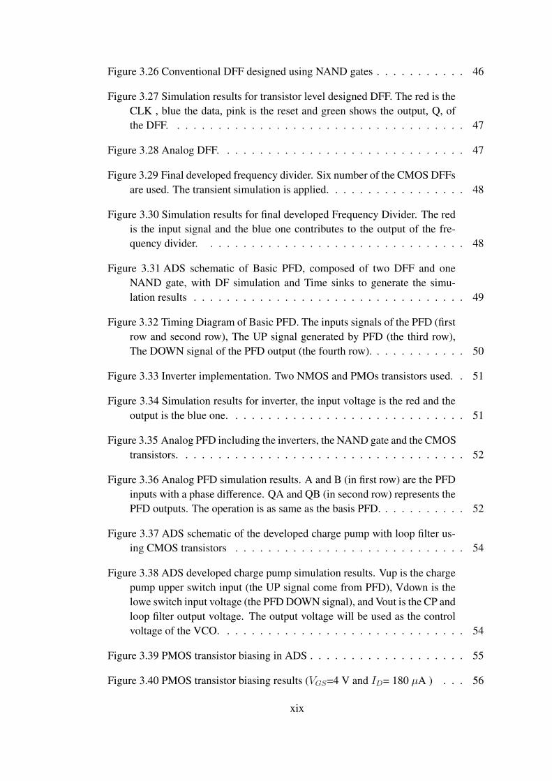
Figure 3.26 Conventional DFF designed using NAND gates . . . . . . . . . . . 46
Figure 3.27 Simulation results for transistor level designed DFF. The red is theCLK , blue the data, pink is the reset and green shows the output, Q, ofthe DFF. . . . . . . . . . . . . . . . . . . . . . . . . . . . . . . . . . . . 47
Figure 3.28 Analog DFF. . . . . . . . . . . . . . . . . . . . . . . . . . . . . . 47
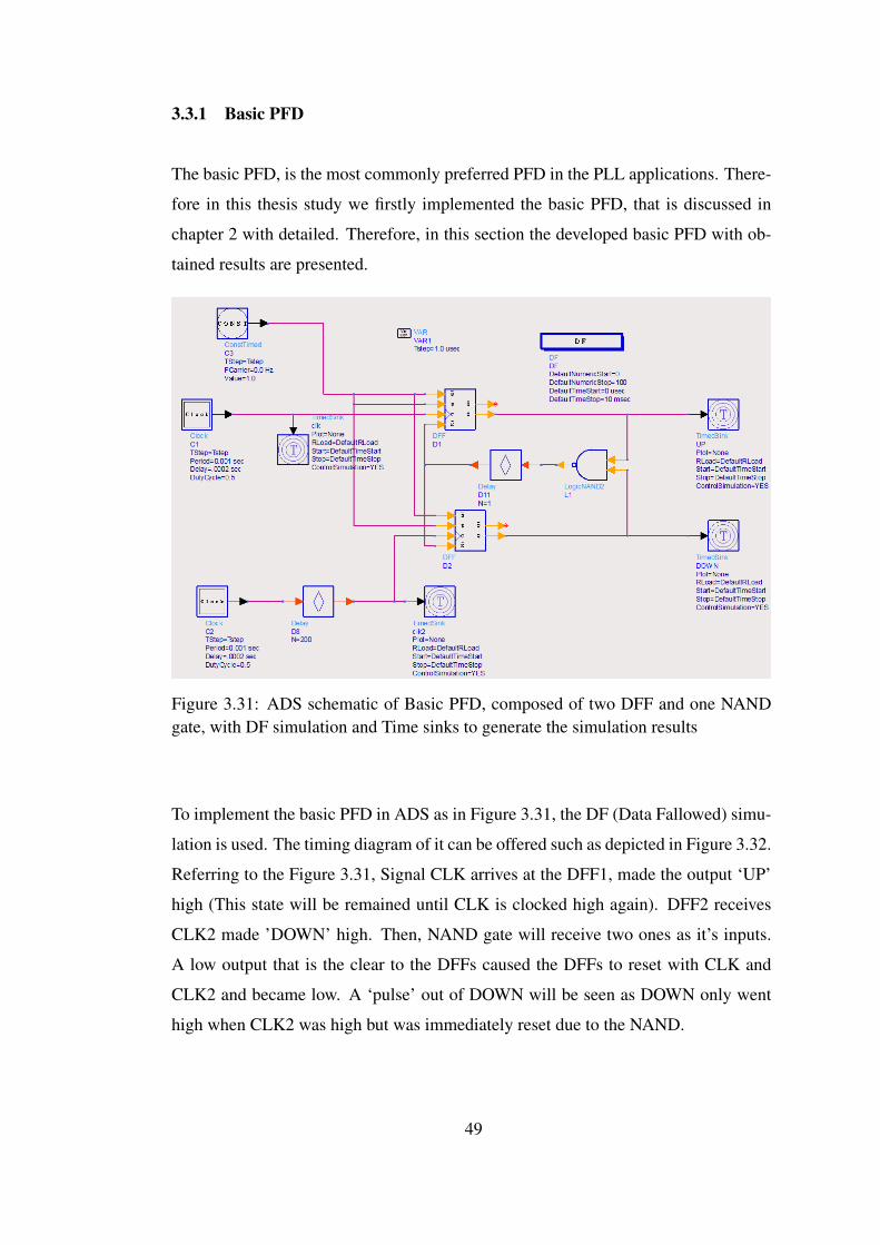
Figure 3.29 Final developed frequency divider. Six number of the CMOS DFFsare used. The transient simulation is applied. . . . . . . . . . . . . . . . . 48
Figure 3.30 Simulation results for final developed Frequency Divider. The redis the input signal and the blue one contributes to the output of the fre-quency divider. . . . . . . . . . . . . . . . . . . . . . . . . . . . . . . . 48
Figure 3.31 ADS schematic of Basic PFD, composed of two DFF and oneNAND gate, with DF simulation and Time sinks to generate the simu-lation results . . . . . . . . . . . . . . . . . . . . . . . . . . . . . . . . . 49
Figure 3.32 Timing Diagram of Basic PFD. The inputs signals of the PFD (firstrow and second row), The UP signal generated by PFD (the third row),The DOWN signal of the PFD output (the fourth row). . . . . . . . . . . . 50
Figure 3.33 Inverter implementation. Two NMOS and PMOs transistors used. . 51
Figure 3.34 Simulation results for inverter, the input voltage is the red and theoutput is the blue one. . . . . . . . . . . . . . . . . . . . . . . . . . . . . 51
Figure 3.35 Analog PFD including the inverters, the NAND gate and the CMOStransistors. . . . . . . . . . . . . . . . . . . . . . . . . . . . . . . . . . . 52
Figure 3.36 Analog PFD simulation results. A and B (in first row) are the PFDinputs with a phase difference. QA and QB (in second row) represents thePFD outputs. The operation is as same as the basis PFD. . . . . . . . . . . 52
Figure 3.37 ADS schematic of the developed charge pump with loop filter us-ing CMOS transistors . . . . . . . . . . . . . . . . . . . . . . . . . . . . 54
Figure 3.38 ADS developed charge pump simulation results. Vup is the chargepump upper switch input (the UP signal come from PFD), Vdown is thelowe switch input voltage (the PFD DOWN signal), and Vout is the CP andloop filter output voltage. The output voltage will be used as the controlvoltage of the VCO. . . . . . . . . . . . . . . . . . . . . . . . . . . . . . 54
Figure 3.39 PMOS transistor biasing in ADS . . . . . . . . . . . . . . . . . . . 55
Figure 3.40 PMOS transistor biasing results (VGS=4 V and ID= 180 µA ) . . . 56
xix
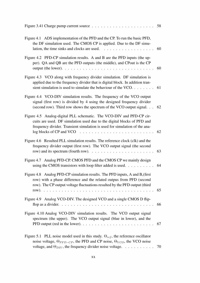
Figure 3.41 Charge pump current source . . . . . . . . . . . . . . . . . . . . . 58
Figure 4.1 ADS implementation of the PFD and the CP. To run the basic PFD,the DF simulation used. The CMOS CP is applied. Due to the DF simu-lation, the time sinks and clocks are used. . . . . . . . . . . . . . . . . . 60
Figure 4.2 PFD-CP simulation results. A and B are the PFD inputs (the up-per). QA and QB are the PFD outputs (the middle), and CPout is the CPoutput (the lower). . . . . . . . . . . . . . . . . . . . . . . . . . . . . . . 60
Figure 4.3 VCO along with frequency divider simulation. DF simulation isapplied due to the frequency divider that is digital block. In addition tran-sient simulation is used to simulate the behaviour of the VCO. . . . . . . . 61
Figure 4.4 VCO-DIV simulation results. The frequency of the VCO outputsignal (first row) is divided by 4 using the designed frequency divider(second row). Third row shows the spectrum of the VCO output signal. . . 62
Figure 4.5 Analog-digital PLL schematic. The VCO-DIV and PFD-CP cir-cuits are used. DF simulation used due to the digital blocks of PFD andfrequency divider. Transient simulation is used for simulation of the ana-log blocks of CP and VCO . . . . . . . . . . . . . . . . . . . . . . . . . 62
Figure 4.6 Resulted PLL simulation results. The reference clock (clk) and thefrequency divider output (first row). The VCO output signal (the secondrow) and its spectrum (fourth row). . . . . . . . . . . . . . . . . . . . . . 63
Figure 4.7 Analog PFD-CP. CMOS PFD and the CMOS CP we mainly designusing the CMOS transistors with loop filter added is used. . . . . . . . . . 64
Figure 4.8 Analog PFD-CP simulation results. The PFD inputs, A and B,(firstrow) with a phase difference and the related outpus from PFD (secondrow). The CP output voltage fluctuations resulted by the PFD output (thirdrow). . . . . . . . . . . . . . . . . . . . . . . . . . . . . . . . . . . . . . 65
Figure 4.9 Analog VCO-DIV. The designed VCO and a single CMOS D flip-flop as a divider. . . . . . . . . . . . . . . . . . . . . . . . . . . . . . . . 66
Figure 4.10 Analog VCO-DIV simulation results. The VCO output signalspectrum (the upper). The VCO output signal (blue in lower), and thePFD output (red in the lower). . . . . . . . . . . . . . . . . . . . . . . . . 67
Figure 5.1 PLL noise model used in this study. Θref , the reference oscillatornoise voltage, ΘPFD−CP , the PFD and CP noise, ΘV CO, the VCO noisevoltage, and ΘDIV , the frequency divider noise voltage. . . . . . . . . . . 70
xx
Figure 5.2 Applied VCO gain or sensitivity. The result of the HB simulationon the designed VCO, to see the frequency changes of the VCO with thecontrol voltage variations. The line is applied, to approximate the linearregion. . . . . . . . . . . . . . . . . . . . . . . . . . . . . . . . . . . . . 71
Figure 5.3 VCO noise analysis. The HB noise controller is used along withthe HB simulation. To make the phase noise simulation possible, the noiseoption in HB simulation is activated. . . . . . . . . . . . . . . . . . . . . 72
Figure 5.4 Simulation results for VCO noise analysis, the noise voltages ofthe VCO (the first row left), the phase noise of VCO in SSB spectrum (thefirst row right), the phase noise values versus noise frequency in table (thesecond row left), the phase noise in dBc/Hz (the second row right). . . . . 73
Figure 5.5 PFD-CP noise analysis. The AC analysis is applied to achieve thephase noise analysis. . . . . . . . . . . . . . . . . . . . . . . . . . . . . . 74
Figure 5.6 Simulation results for PFD-CP noise analysis. The noise voltagesof the PFD and CP (the lower left), the phase noise of the PFD and CP inSSB spectrum (the upper left), and the right one shows the values of thePFD and CP noise voltages versus frequency . . . . . . . . . . . . . . . . 75
Figure 5.7 Frequency divider noise analysis. The divider ratio is 64, so 6 Dflip-flops are used. The AC analysis is applied to simulate the phase noise. 76
Figure 5.8 Simulation results for frequency divider noise analysis. (the fistrow left) noise voltages of the frequency divider, (the fist row right) phasenoise of the frequency divider in SSB spectrum, (the second row) givesthe noise voltage values of the frequency divider in table. . . . . . . . . . 77
Figure 5.9 CPPLL components noise models. Noise model of the VCO (thefist row left), noise model of the frequency divider (the fist row right) andnoise model of the PFD and CP (second row ). . . . . . . . . . . . . . . . 78
Figure 5.10 PLL noise analysis. Each Data Access Component (DAC), in thiscircuit, contains the noise data, we have saved using the noise voltagevalues that are shown in tables for each block of the PLL. The AC nalysisis applied to get the phase noise analysis of the PLL. . . . . . . . . . . . . 79
Figure 5.11 Simulation results for the CPPLL noise analysis. . . . . . . . . . . 80
Figure 5.12 Simulation results for the CPPLL noise analysis. Phase noise com-parison between the implemented VCO and the resultant PLL. . . . . . . . 80
Figure 5.13 Noise analysis of the CPPLL considering the reference oscillator’snoise. . . . . . . . . . . . . . . . . . . . . . . . . . . . . . . . . . . . . . 81
xxi
Figure 5.14 Simulation results for the CPPLL noise analysis. . . . . . . . . . . 82
Figure 5.15 Simulation results for the CPPLL noise analysis. Phase noise com-parison between the implemented VCO and the resultant PLL. . . . . . . . 82
xxii

LIST OF ABBREVIATIONS
ADPLL All-Digital PLL
ADS Advanced Design System
BW Band Width
C Capacitor
CCO Current Controlled Oscillator
CMOS Complementary Metal Oxide Semiconductor
CMFB Common Mode Feed Back
CP Charge Pump
CPPLL Charge Pump PLL
CSA Current Steering Amplifier
DCO Digitally Controlled Oscillator
DF Data Followed
DFF D-Flip-Flop
DPLL Digital PLL
FEPFD Falling-Edge PFD
HB Harmonic Balance
HEMT High Electron Mobility Transistor
ILD Injection-Locking-Divider
LC Inductor Capacitor
LPF Low Pass Filter
LPLL Linear PLL
MWCNT Multi Wire Carbon Nano Tube
MPTPFD Modified Precharge Type PFD
NDR Negative Differential Resistance
NMOS N-channel Metal Oxide Semiconductor
NRZ None Return to Zero
PD Phase Detector
PFD Phase Frequency Detector
xxiii
PLL Phase Locked Loop
PMOS P-channel Metal Oxide Semiconductor
R Resistor
RF Radio Frequency
SR Set-Reset
SRAM Static Random Access Memory
SymFET Symmetric graphene tunneling Field Effect Transistor
TSPC True-Single-Phase-Clocking
VCO Voltage Controlled Oscillator
xxiv
CHAPTER 1
INTRODUCTION
1.1 Motivation
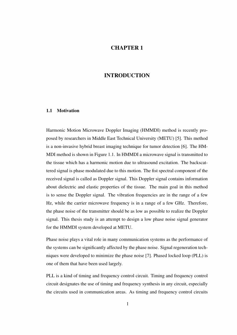
Harmonic Motion Microwave Doppler Imaging (HMMDI) method is recently pro-
posed by researchers in Middle East Technical University (METU) [5]. This method
is a non-invasive hybrid breast imaging technique for tumor detection [6]. The HM-
MDI method is shown in Figure 1.1. In HMMDI a microwave signal is transmitted to
the tissue which has a harmonic motion due to ultrasound excitation. The backscat-
tered signal is phase modulated due to this motion. The fist spectral component of the
received signal is called as Doppler signal. This Doppler signal contains information
about dielectric and elastic properties of the tissue. The main goal in this method
is to sense the Doppler signal. The vibration frequencies are in the range of a few
Hz, while the carrier microwave frequency is in a range of a few GHz. Therefore,
the phase noise of the transmitter should be as low as possible to realize the Doppler
signal. This thesis study is an attempt to design a low phase noise signal generator
for the HMMDI system developed at METU.
Phase noise plays a vital role in many communication systems as the performance of
the systems can be significantly affected by the phase noise. Signal regeneration tech-
niques were developed to minimize the phase noise [7]. Phased locked loop (PLL) is
one of them that have been used largely.
PLL is a kind of timing and frequency control circuit. Timing and frequency control
circuit designates the use of timing and frequency synthesis in any circuit, especially
the circuits used in communication areas. As timing and frequency control circuits
1
Figure 1.1: Harmonic Motion Microwave Doppler Imaging
are used everywhere, including our laptops and mobile devices for time and frequency
synchronization purposes, the importance of these circuits in today’s world can not be
ignored. The timing and frequencies of input signal and feedback signal are matched
using these circuits, as a result, a signal in phase with the input signal is generated. A
PLL tracks phase noise of the reference frequency within its loop bandwidth, relaxing
the close-in phase noise requirements of the VCO. For PLL applications, the reference
input signal generated by a high purity crystal oscillator has very low phase noise,
and the PLL serves to lock the output frequency on a multiple of the input frequency.
Negative feedback path made the PLL operates by trying to lock to the phase of a
very stable input signal.
Phase-locked loops can be used, for example, to generate stable output frequency
signals from a fixed low-frequency signal. In a phase locked loop, the error signal
from the phase detector is the difference between the input signal and the feedback
signal. Implementation of these signals in multichannel wireless systems is also a
tedious task. A multichannel wireless system utilizes multi-band frequencies in a
single system for different applications of different frequencies. In this case, the
timing and frequency circuit plays a vital role in choosing the frequency which is
suitable for a particular application among the bands of frequencies present in the
system.
2
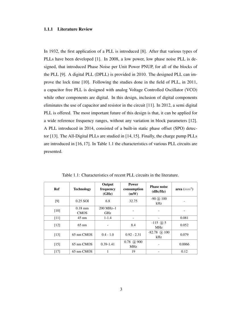
1.1.1 Literature Review
In 1932, the first application of a PLL is introduced [8]. After that various types of
PLLs have been developed [1]. In 2008, a low power, low phase noise PLL is de-
signed, that introduced Phase Noise per Unit Power PNUP, for all of the blocks of
the PLL [9]. A digital PLL (DPLL) is provided in 2010. The designed PLL can im-
prove the lock time [10]. Following the studies done in the field of PLL, in 2011,
a capacitor free PLL is designed with analog Voltage Controlled Oscillator (VCO)
while other components are digital. In this design, inclusion of digital components
eliminates the use of capacitor and resistor in the circuit [11]. In 2012, a semi digital
PLL is offered. The most important future of this design is that, it can be applied for
a wide reference frequency ranges, without any variation in block parameters [12].
A PLL introduced in 2014, consisted of a built-in static phase offset (SPO) detec-
tor [13]. The All-Digital PLLs are studied in [14,15]. Finally, the charge pump PLLs
are introduced in [16, 17]. In Table 1.1 the characteristics of various PLL circuits are
presented.
Table 1.1: Characteristics of recent PLL circuits in the literature.
Ref TechnologyOutput
frequency(GHz)
Powerconsumption
(mW)
Phase noise(dBc/Hz)
area (mm2)
[9] 0.25 SOI 6.8 32.75-90 a© 100
kHz-
[10]0.18 mmCMOS
200 MHz–1GHz
- - -
[11] 45 nm 1-1.4 - - 0.081
[12] 65 nm - 8.4-115 a© 5
MHz0.052
[13] 65 nm CMOS 0.4 - 1.0 0.92 - 2.31-82.78 a© 100
kHz0.079
[15] 65 nm CMOS 0.39-1.410.78 a© 900
MHz- 0.0066
[17] 65 nm CMOS 1 19 - 0.12
3
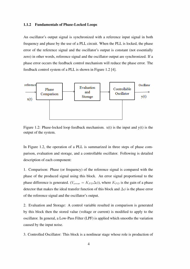
1.1.2 Fundamentals of Phase-Locked Loops
An oscillator’s output signal is synchronized with a reference input signal in both
frequency and phase by the use of a PLL circuit. When the PLL is locked, the phase
error of the reference signal and the oscillator’s output is constant (not essentially
zero) in other words, reference signal and the oscillator output are synchronized. If a
phase error occurs the feedback control mechanism will reduce the phase error. The
feedback control system of a PLL is shown in Figure 1.2 [4].
Figure 1.2: Phase-locked loop feedback mechanism. x(t) is the input and y(t) is theoutput of the system.
In Figure 1.2, the operation of a PLL is summarized in three steps of phase com-
parison, evaluation and storage, and a controllable oscillator. Following is detailed
description of each component:
1. Comparison: Phase (or frequency) of the reference signal is compared with the
phase of the produced signal using this block. An error signal proportional to the
phase difference is generated. (Verror = KPD∆φ), where KPD is the gain of a phase
detector that makes the ideal transfer function of this block and ∆φ is the phase error
of the reference signal and the oscillator’s output.
2. Evaluation and Storage: A control variable resulted in comparison is generated
by this block then the stored value (voltage or current) is modified to apply to the
oscillator. In general, a Low-Pass Filter (LPF) is applied which smooths the variation
caused by the input noise.
3. Controlled Oscillator: This block is a nonlinear stage whose role is production of
4
an oscillation that is frequency controlled using a lower frequency voltage or current
input. The controlled oscillator can be a Voltage Controlled Oscillator (VCO) or a
Current Controlled Oscillator (CCO).
1.1.3 Phase-Locked Loop Types
As depicted in Table1.2 [4], PLLs are divided in 4 groups that will be reviewed as
follows:
Table 1.2: PLL classification
PLL Type Comparison Evaluation Storage Oscillator
Linear PLL(LPLL)
Analogmultiplier
LPFAnalog
voltage onfilter capacitor
VCO
Digital PLL(DPLL)
EXOR PD orJKPD
LPFAnalog
voltage onfilter capacitor
VCO
Charge-pumpPLL (CPPLL)
PFDCharge pump
and LPF
Analogvoltage on
filter capacitorVCO
All-digitalPLL (ADPLL)
EXOR PD orJKPD or PFD
Digital LPF Digital word
Digitallycontrolledoscillator(DCO)
1.1.3.1 Linear PLL
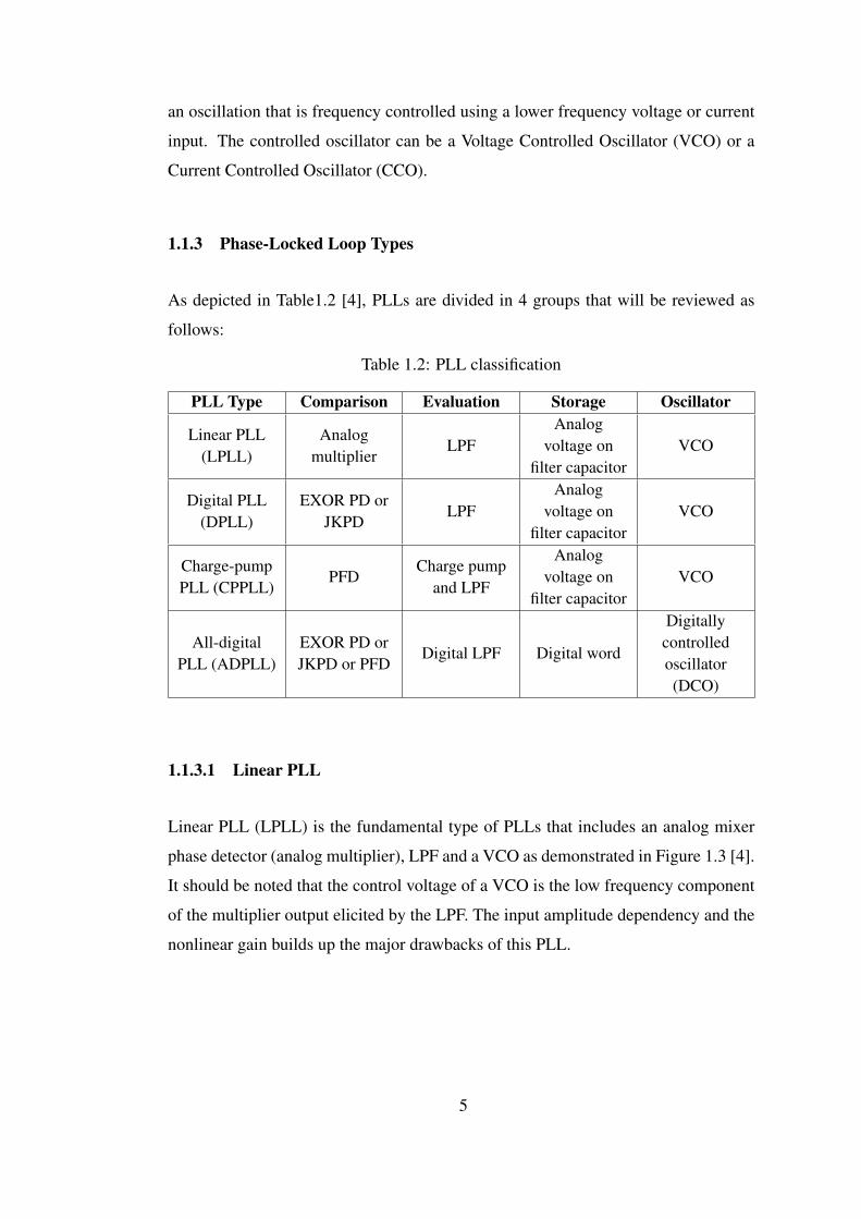
Linear PLL (LPLL) is the fundamental type of PLLs that includes an analog mixer
phase detector (analog multiplier), LPF and a VCO as demonstrated in Figure 1.3 [4].
It should be noted that the control voltage of a VCO is the low frequency component
of the multiplier output elicited by the LPF. The input amplitude dependency and the
nonlinear gain builds up the major drawbacks of this PLL.
5
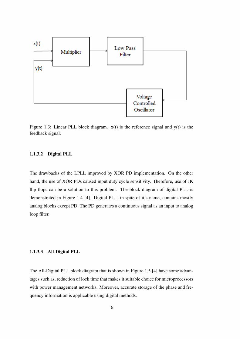
Figure 1.3: Linear PLL block diagram. x(t) is the reference signal and y(t) is thefeedback signal.
1.1.3.2 Digital PLL
The drawbacks of the LPLL improved by XOR PD implementation. On the other
hand, the use of XOR PDs caused input duty cycle sensitivity. Therefore, use of JK
flip flops can be a solution to this problem. The block diagram of digital PLL is
demonstrated in Figure 1.4 [4]. Digital PLL, in spite of it’s name, contains mostly
analog blocks except PD. The PD generates a continuous signal as an input to analog
loop filter.
1.1.3.3 All-Digital PLL
The All-Digital PLL block diagram that is shown in Figure 1.5 [4] have some advan-
tages such as, reduction of lock time that makes it suitable choice for microprocessors
with power management networks. Moreover, accurate storage of the phase and fre-
quency information is applicable using digital methods.
6
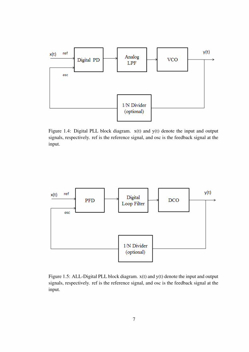
Figure 1.4: Digital PLL block diagram. x(t) and y(t) denote the input and outputsignals, respectively. ref is the reference signal, and osc is the feedback signal at theinput.
Figure 1.5: ALL-Digital PLL block diagram. x(t) and y(t) denote the input and outputsignals, respectively. ref is the reference signal, and osc is the feedback signal at theinput.
7
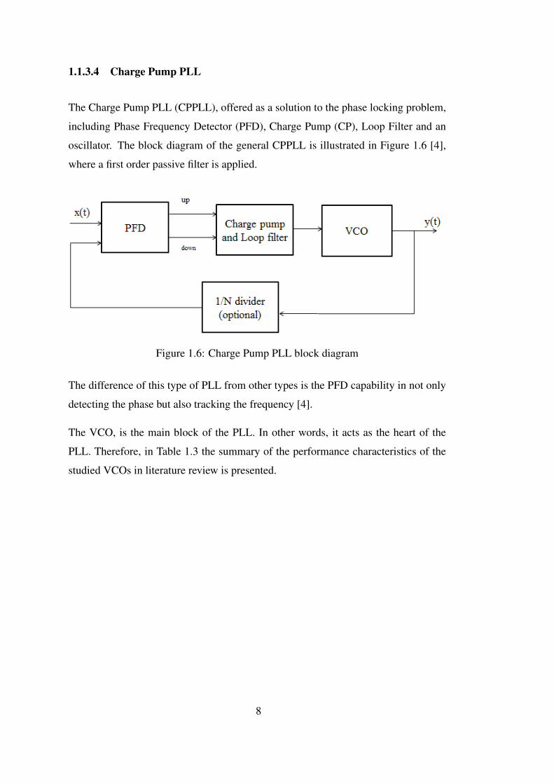
1.1.3.4 Charge Pump PLL
The Charge Pump PLL (CPPLL), offered as a solution to the phase locking problem,
including Phase Frequency Detector (PFD), Charge Pump (CP), Loop Filter and an
oscillator. The block diagram of the general CPPLL is illustrated in Figure 1.6 [4],
where a first order passive filter is applied.
Figure 1.6: Charge Pump PLL block diagram
The difference of this type of PLL from other types is the PFD capability in not only
detecting the phase but also tracking the frequency [4].
The VCO, is the main block of the PLL. In other words, it acts as the heart of the
PLL. Therefore, in Table 1.3 the summary of the performance characteristics of the
studied VCOs in literature review is presented.
8
Tabl
e1.
3:T
hepe
rfor
man
cech
arac
teri
stic
sof
the
illus
trat
edV
CO
sin
liter
atur
ere
view
Ref
Tech
nolo
gyFr
eq(G
Hz)
Tuni
ngra
nge
(GH
z)D
Cpo
wer
(mw
)Su
pply
(v)
Phas
eno
ise(
dBc/
Hz)
[18]
0.5µ
mG
aAsP
HE
M49
48.7
-49.
775
5-1
00a ©
100k
Hz
[19]
65nm
CM
OS
3.6
-5.
61
-123
a ©60
0kH
z-1
26a ©
800k
Hz
-137
a ©3
MH
z[2
0]Sy
mFE
T3.
05-3
.07
-0.
230.
3-1
17a ©
1M
Hz
[21]
90nm
CM
OS
5.2
4.62
-5.8
1(2
2.9%
)1.
352.
7-1
30.1
a ©60
0kH
z[2
2]0.
18µ
mC
MO
S10
.94
7.5%
0.34
60.
46-1
07.8
a ©1
MH
z[2
3]0.
18µ
mB
iCM
OS
2.4
2.07
-2.7
7(2
9.16
%)
1.7
0.6
-133
.3a ©
1M
Hz
[24]
-24
.29
23.3
-25.
90(1
0.54
%)
--
-88.
34a ©
1M
Hz
24.1
023
.25-
25.7
4(1
0.33
%)
-92.
039
a ©1
MH
z[2
5]0.
25µ
mB
iCM
OS
19.9
415M
Hz(Vtune=0
-5V
)22
.35
2.5
-106
a ©1
MH
zSi
Ge:
C20
.06
130M
Hz
(Vtune=0
-5V
)12
.52.
5-9
6.5
a ©1
MH
z[2
6]0.
18µ
mC
MO
S2.
162.
12-2
.25
--
-110
a ©1
MH
z[2
7]0.
35µ
mB
iCM
OS
2.33
26%
-2.
5-1
21f c
=1.9
1a ©
600
kHz
-117f c
=2.0
3a ©
600
kHz
-115f c
=2.6
3a ©
600
kHz
9
In this work, having a pure signal with low phase noise is the main goals to achieve
the desired results at the proceeding steps. Therefore, design of a low phase noise
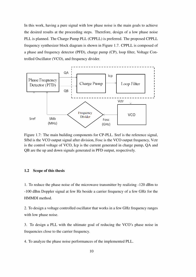
PLL is planned. The Charge Pump PLL (CPPLL) is preferred. The proposed CPPLL
frequency synthesizer block diagram is shown in Figure 1.7. CPPLL is composed of
a phase and frequency detector (PFD), charge pump (CP), loop filter, Voltage Con-
trolled Oscillator (VCO), and frequency divider.
Figure 1.7: The main building components for CP-PLL. Sref is the reference signal,Sfbd is the VCO output signal after division, Fosc is the VCO output frequency, Vctris the control voltage of VCO, Icp is the current generated in charge pump, QA andQB are the up and down signals generated in PFD output, respectively.
1.2 Scope of this thesis
1. To reduce the phase noise of the microwave transmitter by realizing -120 dBm to
-100 dBm Doppler signal at few Hz beside a carrier frequency of a few GHz for the
HMMDI method.
2. To design a voltage controlled oscillator that works in a few GHz frequency ranges
with low phase noise.
3. To design a PLL with the ultimate goal of reducing the VCO’s phase noise in
frequencies close to the carrier frequency.
4. To analyze the phase noise performances of the implemented PLL.
10
1.3 Thesis Organization
In chapter 2, the basic concepts of the PLL will be studied. In this chapter, a review
of the fundamentals of the PLL will be offered. The VCO basics and the phase noise
concepts will be introduced. A review of the PFD, one of the important components
of the PLL will be offered. The CP and loop filter basics will be studied. The chapter
will be finalized by the review of the frequency divider.
Chapter 3, contains the design of the PLL constructing blocks. In this chapter, first,
the VCO design will be discussed. Then, the frequency divider design and implemen-
tation will be introduced. The phase frequency detector design will be offered next.
Finally, the charge pump and loop filter design will be presented.
In chapter 4, the simulation results of the implemented PLL (using ADS) are pre-
sented. In this chapter the analog-digital PLL will be offered, fist. Then the all-analog
PLL will be presented.
Chapter 5, includes the phase noise analysis of the implemented PLL. The influence
of the PLL on the VCO’s phase noise is discussed in this chapter.
Finally, chapter 6, will provide the conclusion and future works of this study.
11

12
CHAPTER 2
PHASE-LOCKED LOOPS
In this chapter, the basic concepts of the PLL will be studied. A review of the fun-
damentals of the PLL will be offered. The VCO basics and the phase noise concepts
will be introduced. A review of the PFD, one of the important components of the
PLL will be offered. The CP and loop filter basics will be studied. The chapter will
be finalized by the review of the frequency divider.
2.1 Basic concepts
2.1.1 Voltage Controlled Oscillator
An ideal VCO is characterised as 2.1
ωout = ω0 +KV COVcont (2.1)
where ω0 is the free running frequency at Vcont=0 and KV CO is called as the gain or
sensitivity of the oscillator [1].
The VCO is considered as a time invariant system in study of PLLs. In this system,
the control voltage is defined as the input of the system and the excess phase of the
carrier is the system’s output. The excess phase can be defined as 2.2
φout(t) = KV CO
∫Vcontdt (2.2)
13
Accordingly, the transfer function of the VCO is
φout
Vcont(s) =
KV CO
s(2.3)
2.1.2 Phase Detector
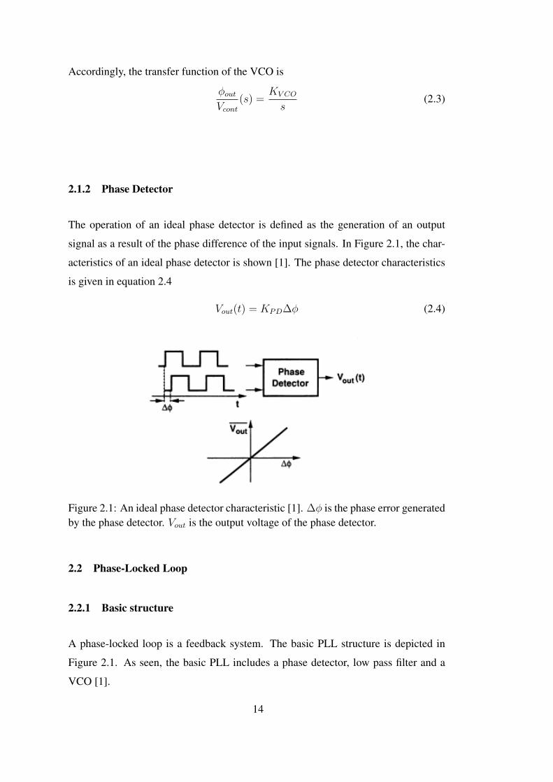
The operation of an ideal phase detector is defined as the generation of an output
signal as a result of the phase difference of the input signals. In Figure 2.1, the char-
acteristics of an ideal phase detector is shown [1]. The phase detector characteristics
is given in equation 2.4
Vout(t) = KPD∆φ (2.4)
Figure 2.1: An ideal phase detector characteristic [1]. ∆φ is the phase error generatedby the phase detector. Vout is the output voltage of the phase detector.
2.2 Phase-Locked Loop
2.2.1 Basic structure
A phase-locked loop is a feedback system. The basic PLL structure is depicted in
Figure 2.1. As seen, the basic PLL includes a phase detector, low pass filter and a
VCO [1].
14
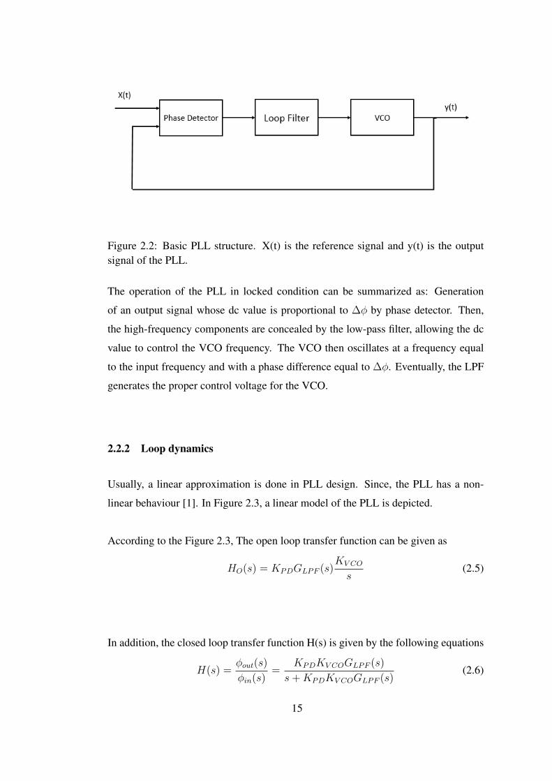
Figure 2.2: Basic PLL structure. X(t) is the reference signal and y(t) is the outputsignal of the PLL.
The operation of the PLL in locked condition can be summarized as: Generation
of an output signal whose dc value is proportional to ∆φ by phase detector. Then,
the high-frequency components are concealed by the low-pass filter, allowing the dc
value to control the VCO frequency. The VCO then oscillates at a frequency equal
to the input frequency and with a phase difference equal to ∆φ. Eventually, the LPF
generates the proper control voltage for the VCO.
2.2.2 Loop dynamics
Usually, a linear approximation is done in PLL design. Since, the PLL has a non-
linear behaviour [1]. In Figure 2.3, a linear model of the PLL is depicted.
According to the Figure 2.3, The open loop transfer function can be given as
HO(s) = KPDGLPF (s)KV CO
s(2.5)
In addition, the closed loop transfer function H(s) is given by the following equations
H(s) =φout(s)
φin(s)=
KPDKV COGLPF (s)
s+KPDKV COGLPF (s)(2.6)
15
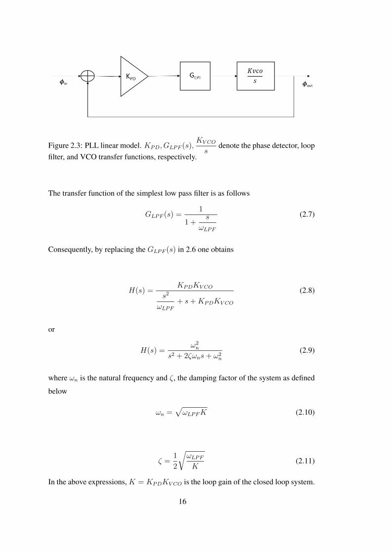
Figure 2.3: PLL linear model. KPD, GLPF (s),KV CO
sdenote the phase detector, loop
filter, and VCO transfer functions, respectively.
The transfer function of the simplest low pass filter is as follows
GLPF (s) =1
1 +s
ωLPF
(2.7)
Consequently, by replacing the GLPF (s) in 2.6 one obtains
H(s) =KPDKV CO
s2
ωLPF
+ s+KPDKV CO
(2.8)
or
H(s) =ω2n
s2 + 2ζωns+ ω2n
(2.9)
where ωn is the natural frequency and ζ , the damping factor of the system as defined
below
ωn =√ωLPFK (2.10)
ζ =1
2
√ωLPF
K(2.11)
In the above expressions, K = KPDKV CO is the loop gain of the closed loop system.
16
2.3 Charge pump PLL
The CPPLL is the preferred PLL type in this work. The CPPLL is reviewed in chapter
1, according to the Figure 1.6 , if a phase error of Φe = Φin−Φvco occurs in the loop,
an average charge pump current ofICP
2πis generated. The control voltage of the VCO
can be changed as given below in equation 2.12
Vctrl(s) =Iφe
2π(R +
1
CP s) (2.12)
Therefore, the closed loop transfer function can be calculated as follows:
H(s) =
IPKV CO
2πCP
(RPCP s+ 1)
s2 +IP2π
KV CO
NRP s+
IP2πCP
KV CO
N
(2.13)
Based on the above equation, ωn and ζ are obtained as follows:
ωn =
√IP
2πCP
KV CO
N(2.14)
ζ =RP
2
√IPCPKV CO
2πN(2.15)
2.4 PLL components
2.4.1 Voltage Controlled Oscillator
One of the most important blocks of PLL is VCO. The out of band phase noise perfor-
mance is determined by VCO. Both ring oscillators and LC oscillators are commonly
used in the GHz range applications. Low phase noise and low power consumption
made LC oscillators more attractive than the ring oscillators. LC oscillator also has
different types such as Colpitts and Hartley. The Colpitts Oscillator is an LC Oscilla-
tor circuit identified by a tapped capacitor configuration. It is commonly used in high
17
frequency communication applications due to low phase noise and the ability of oscil-
lation at high frequencies. Less chip area demand of Colpitts oscillator than most of
the other passive device oscillators made it an attractive component in semiconductor
design [28].
2.4.1.1 General Considerations
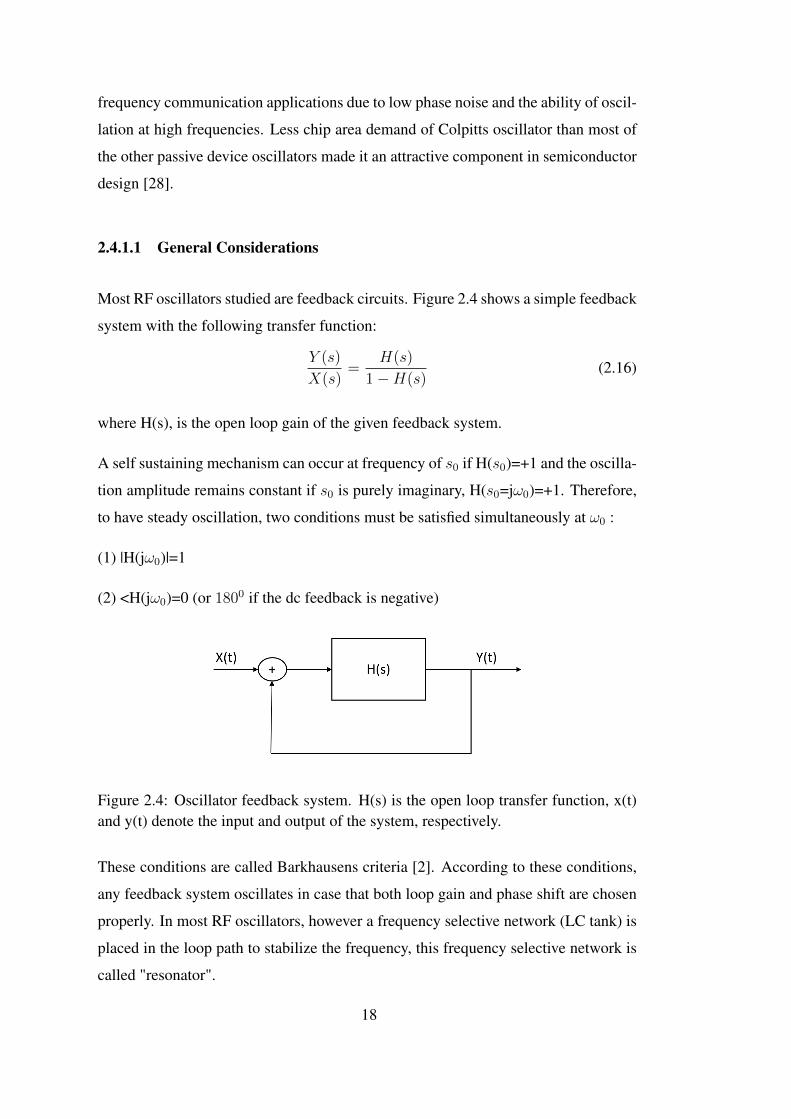
Most RF oscillators studied are feedback circuits. Figure 2.4 shows a simple feedback
system with the following transfer function:
Y (s)
X(s)=
H(s)
1−H(s)(2.16)
where H(s), is the open loop gain of the given feedback system.
A self sustaining mechanism can occur at frequency of s0 if H(s0)=+1 and the oscilla-
tion amplitude remains constant if s0 is purely imaginary, H(s0=jω0)=+1. Therefore,
to have steady oscillation, two conditions must be satisfied simultaneously at ω0 :
(1) |H(jω0)|=1
(2) <H(jω0)=0 (or 1800 if the dc feedback is negative)
Figure 2.4: Oscillator feedback system. H(s) is the open loop transfer function, x(t)and y(t) denote the input and output of the system, respectively.
These conditions are called Barkhausens criteria [2]. According to these conditions,
any feedback system oscillates in case that both loop gain and phase shift are chosen
properly. In most RF oscillators, however a frequency selective network (LC tank) is
placed in the loop path to stabilize the frequency, this frequency selective network is
called "resonator".
18
2.4.1.2 Basic LC Oscillator Topologies
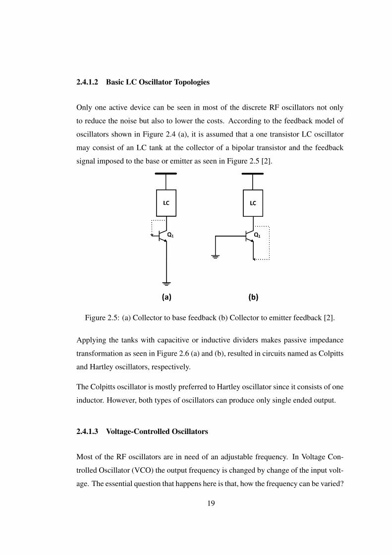
Only one active device can be seen in most of the discrete RF oscillators not only
to reduce the noise but also to lower the costs. According to the feedback model of
oscillators shown in Figure 2.4 (a), it is assumed that a one transistor LC oscillator
may consist of an LC tank at the collector of a bipolar transistor and the feedback
signal imposed to the base or emitter as seen in Figure 2.5 [2].
Figure 2.5: (a) Collector to base feedback (b) Collector to emitter feedback [2].
Applying the tanks with capacitive or inductive dividers makes passive impedance
transformation as seen in Figure 2.6 (a) and (b), resulted in circuits named as Colpitts
and Hartley oscillators, respectively.
The Colpitts oscillator is mostly preferred to Hartley oscillator since it consists of one
inductor. However, both types of oscillators can produce only single ended output.
2.4.1.3 Voltage-Controlled Oscillators
Most of the RF oscillators are in need of an adjustable frequency. In Voltage Con-
trolled Oscillator (VCO) the output frequency is changed by change of the input volt-
age. The essential question that happens here is that, how the frequency can be varied?
19
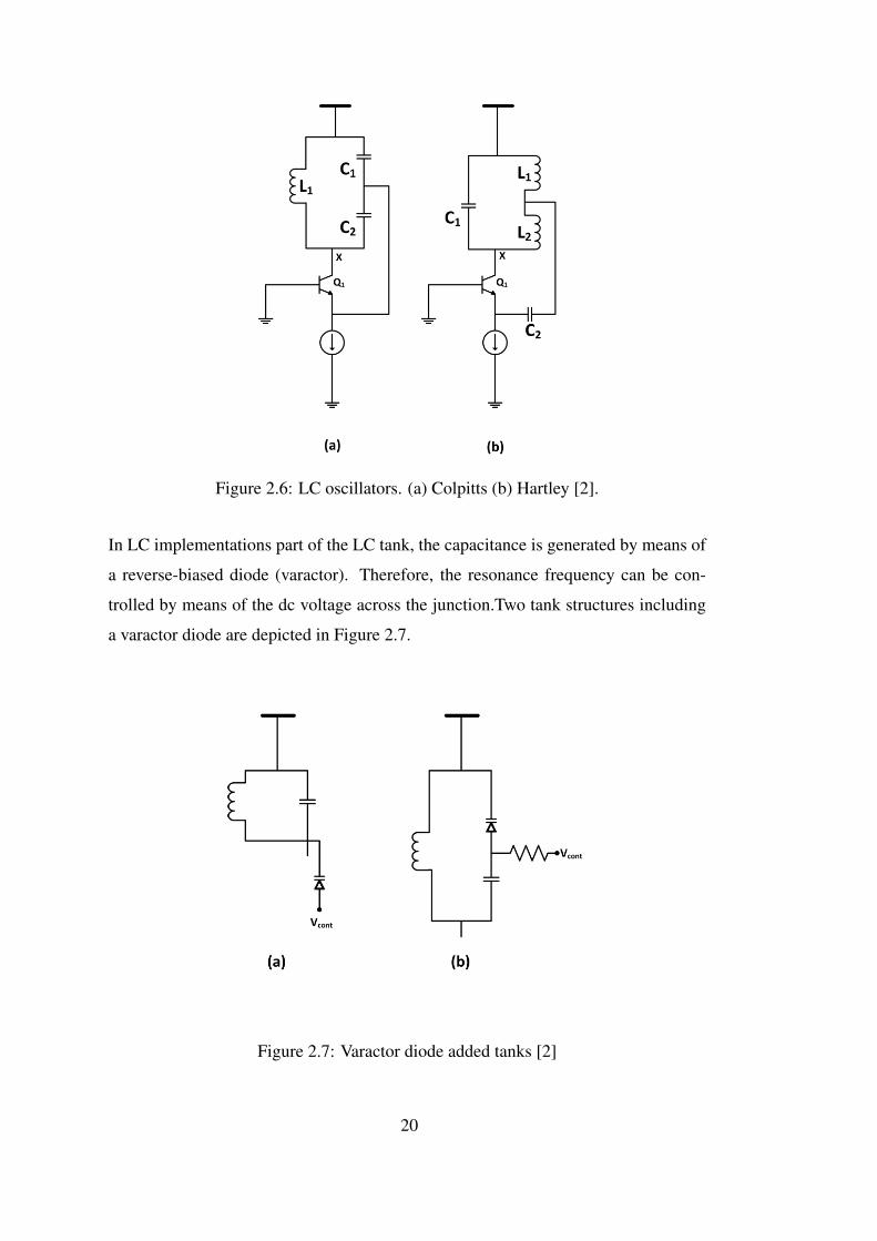
Figure 2.6: LC oscillators. (a) Colpitts (b) Hartley [2].
In LC implementations part of the LC tank, the capacitance is generated by means of
a reverse-biased diode (varactor). Therefore, the resonance frequency can be con-
trolled by means of the dc voltage across the junction.Two tank structures including
a varactor diode are depicted in Figure 2.7.
Figure 2.7: Varactor diode added tanks [2]
20
2.4.2 Phase frequency detector
The PFD role in PLL frequency synthesizer is defined as the detection of the phase
and frequency differences of the reference clock and the internal VCO clock. As soon
as the synthesizer is activated, an unlocked state happened if the divided VCO output
is irrelevant that of the reference. An appropriate output signal is produced by the PFD
according to the phase relationships of the input signals that means one leads or lags
the other. The phase difference or phase error produced by the PFD is altered to a DC
control voltage of the VCO leads to a signal with the desired frequency throughout
the charge pump and low pass loop filter. Various types of PFDs included basic PFD,
Hogg PFD and Alexander PFD are studied in [29]. The CMOS types of PFDs are
studied as conventional PFD in [30,31], Modified Precharged Type PFD (MPTPFD),
provides better speed performance rather than the conventional PFD in [4, 30, 32]. In
addition, the Falling-Edge PFD (FE-PFD ) with a simple structure than the MPTPFD
is studied in [30]. A pass transistor DFF PFD and a latch-based PFD are proposed
in [3]. In this research, we mostly used basic PFD [29,33] and the latch-based PFD [3]
is used and implemented.
2.4.2.1 Basic PFD
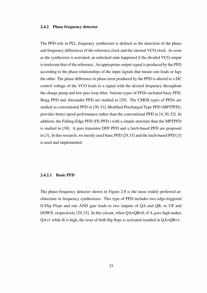
The phase-frequency detector shown in Figure 2.8 is the most widely preferred ar-
chitecture in frequency synthesizers. This type of PFD includes two edge-triggered
D-Flip Flops and one AND gate leads to two outputs of QA and QB, or UP and
DOWN, respectively [29, 33]. In this circuit, when QA=QB=0, if A goes high makes
QA=1 while B is high, the reset of both flip flops is activated resulted in QA=QB=1.
21
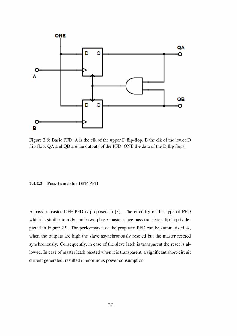
Figure 2.8: Basic PFD. A is the clk of the upper D flip-flop. B the clk of the lower Dflip-flop. QA and QB are the outputs of the PFD. ONE the data of the D flip flops.
2.4.2.2 Pass-transistor DFF PFD
A pass transistor DFF PFD is proposed in [3]. The circuitry of this type of PFD
which is similar to a dynamic two-phase master-slave pass transistor flip flop is de-
picted in Figure 2.9. The performance of the proposed PFD can be summarized as,
when the outputs are high the slave asynchronously reseted but the master reseted
synchronously. Consequently, in case of the slave latch is transparent the reset is al-
lowed. In case of master latch reseted when it is transparent, a significant short-circuit
current generated, resulted in enormous power consumption.
22
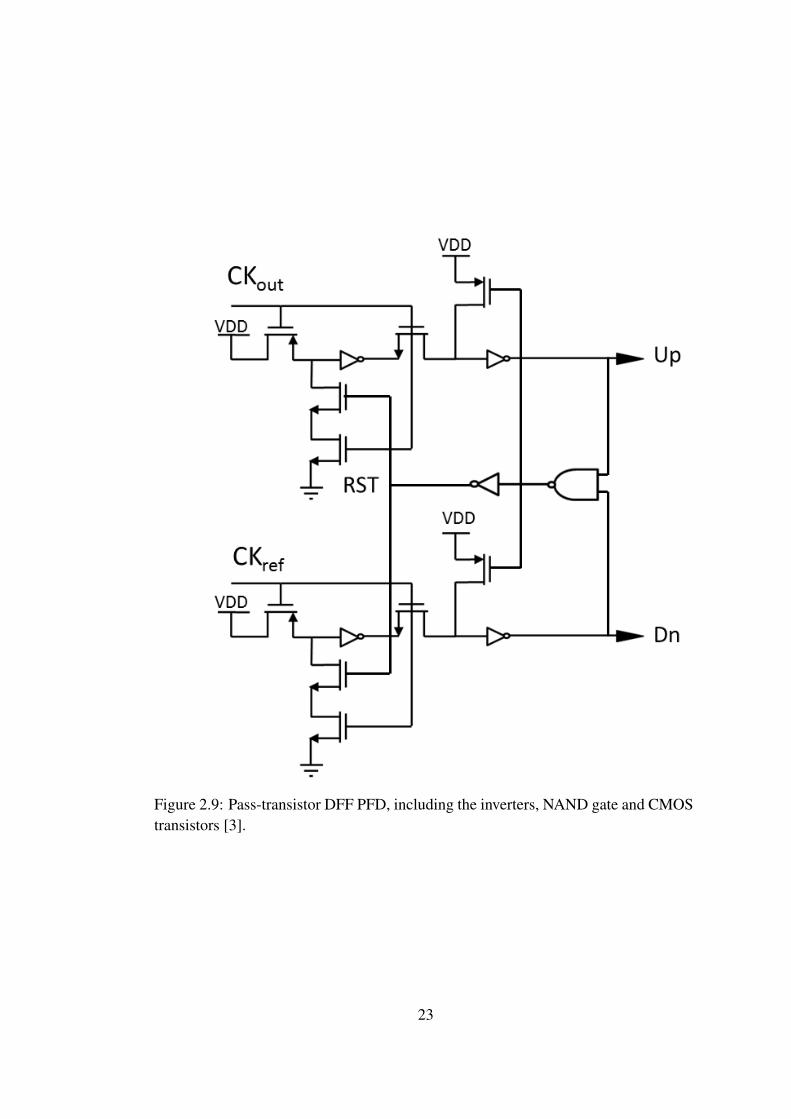
Figure 2.9: Pass-transistor DFF PFD, including the inverters, NAND gate and CMOStransistors [3].
23

2.4.3 Charge pump and loop filter
PFD driven charge pump produces current pulses that charge or discharge the loop
filter capacitor. Figure 2.10 shows a simple charge pump structure. Effective charge
pump requirements can be summarized as [34]:
1-Charge/discharge current should be equal at any output node.
2-Charge injection and feed-through (due to switching) should be minimized at the
output.
3-Charge sharing between output node and any floating node should be minimized.
Figure 2.10: Basic charge Pump.
Current mismatching is defined as the magnitude difference of charging and discharg-
ing currents [35]. Single-ended charge pumps, charge pump with an active amplifier
and charge pump with current steering switches are studied in [4] and [34]. In addi-
tion, the differential charge pumps are presented in [36, 37] and [38]. In this thesis,
we try to develop a charge pump as the basic charge pump shown in Figure 2.10 using
CMOS transistors as single-ended charge pumps.
24

2.4.3.1 Single-Ended Charge Pumps
A single ended charge pump is most commonly preferred since it leads to lower power
consumption and autonomous operation with no additional loop filter. In Figure 2.11
a simple implementation of the single-ended charge pump and its variations are de-
picted [4].
Figure 2.11: Single-ended charge pump diversity [4].
In Figure 2.11 (a), a replica bias circuit from a reference current generates the bias
voltages of the Vbp and Vbn resulted in best matching between IUP and IDWN . The
circuit provided in Figure 2.11 (a) has some drawbacks included the charge injection
to the output node and charge sharing. Adding a drain to source shorted dummy tran-
sistor on each side of the switch transistor or as depicted in Figure 2.11 (b) shifting
the switch transistors towards the rails can be a solution to the former problem. Any-
how, for both designs due to the existence of the floating nodes in certain node the
charge sharing problem still remains. In Figure 2.11 (c), a so modified circuitry con-
tains charge removal transistors to abolish the charge sharing is offered. The provided
circuitry made a large reduction in phase offset. Furthermore, the intrinsic 1f
noise
decreased remarkably.
25
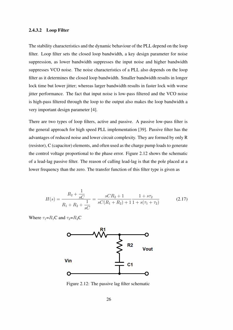
2.4.3.2 Loop Filter
The stability characteristics and the dynamic behaviour of the PLL depend on the loop
filter. Loop filter sets the closed loop bandwidth, a key design parameter for noise
suppression, as lower bandwidth suppresses the input noise and higher bandwidth
suppresses VCO noise. The noise characteristics of a PLL also depends on the loop
filter as it determines the closed loop bandwidth. Smaller bandwidth results in longer
lock time but lower jitter; whereas larger bandwidth results in faster lock with worse
jitter performance. The fact that input noise is low-pass filtered and the VCO noise
is high-pass filtered through the loop to the output also makes the loop bandwidth a
very important design parameter [4].
There are two types of loop filters, active and passive. A passive low-pass filter is
the general approach for high speed PLL implementation [39]. Passive filter has the
advantages of reduced noise and lower circuit complexity. They are formed by only R
(resistor), C (capacitor) elements, and often used as the charge pump loads to generate
the control voltage proportional to the phase error. Figure 2.12 shows the schematic
of a lead-lag passive filter. The reason of calling lead-lag is that the pole placed at a
lower frequency than the zero. The transfer function of this filter type is given as
H(s) =R2 +
1
sC
R1 +R2 +1
sC
=sCR2 + 1
sC(R1 +R2) + 1
1 + sτ21 + s(τ1 + τ2)
(2.17)
Where τ1=R1C and τ2=R2C
Figure 2.12: The passive lag filter schematic
26
2.4.4 Frequency divider
The frequency divider chain of the PLL frequency synthesizer plays an important
role in modern integrated transceivers operating at microwave frequencies. When the
VCO output frequency is in the order of several GHz, implementing the frequency di-
vision at such high frequencies is a challenge. Different approaches can be attempted
depending on the frequency that needs to be divided. In other words, the frequency
divider role is production of a clock signal runs many times faster than the reference
clock [40].
Design of a digital counter included a digital logic resetting the counter after a num-
ber of input clock cycles equal to the division ratio have been counted is the simplest
approach to implement a clock frequency division. Limited maximum frequency of
operation due to the digital logic with which the counter is implemented builds up the
most critic disadvantage of this solution. Such kind of frequency divider generally
performs up to few GHz (typically no more than 3-4 GHz). However, low power con-
sumption, and the possibility of being programmable by dynamically changing the
resetting logic (and thus the division ratio) contributes to the most important advan-
tages of this type of frequency divider.
Applying a purely analog solution is usually preferred in case of higher frequency
division [41]. D-flip flops are commonly used as divider. The Yuan-Svensson D-
FF and the Huang-Rogenmoser D-FF are presented in [39]. In addition, high speed
divide-by-two and dual-modulus dividers are introduced [2]. In [41], the multi GHz
frequency dividers are addressed.
2.4.4.1 CMOS D-FF
Circuit schematic of the conventional D flip-flop is as shown in figure 2.13. When
clk=0, inverted D get to the node X. Node Y charged up to the VDD and M7 and
M8 get off. Therefore, when the clk is in low state, the input of the final inverter
holds its previous value and the output Q is stable. When the clk=1, X=1, node Y is
discharged. The third inverter M8-M9 is on during the high phase and the node value
of Y is passed to the output Q.
27

Figure 2.13: Conventional D flip-flop
28
CHAPTER 3
PLL BLOCKS DESIGN AND ANALYSIS
In this chapter, the design of the constructing blocks of the PLL will be presented.
First, the VCO design will be discussed. Then, the frequency divider design and
implementation will be introduced. The phase frequency detector design will be of-
fered next. Finally, the charge pump and loop filter design will be presented. The
simulations in this chapter are implemented in Advanced Designed System (ADS).
3.1 The VCO design proposed in this thesis study
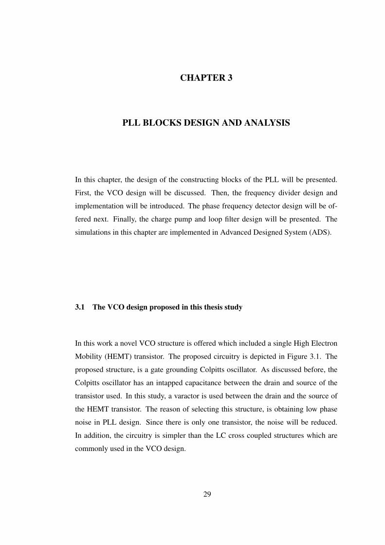
In this work a novel VCO structure is offered which included a single High Electron
Mobility (HEMT) transistor. The proposed circuitry is depicted in Figure 3.1. The
proposed structure, is a gate grounding Colpitts oscillator. As discussed before, the
Colpitts oscillator has an intapped capacitance between the drain and source of the
transistor used. In this study, a varactor is used between the drain and the source of
the HEMT transistor. The reason of selecting this structure, is obtaining low phase
noise in PLL design. Since there is only one transistor, the noise will be reduced.
In addition, the circuitry is simpler than the LC cross coupled structures which are
commonly used in the VCO design.
29
Figure 3.1: Schematic of the proposed VCO.
3.1.1 HEMT transistor
The HEMT is a form of field effect transistor, FET, that is used to provide very high
levels of performance at microwave frequencies. The HEMT offers a combination
of low noise figure combined with the ability to operate at the very high microwave
frequencies. Accordingly, the device is used in areas of RF design where high perfor-
mance is required at very high RF frequencies. Since the operation frequency of the
HMMDI is in the range of a few GHz, HEMT is preferred in the design of VCO. The
HEMT transistor biasing is demonstrated in Figure 3.2.
Figure 3.2: Applied HEMT transistor biasing in ADS
30
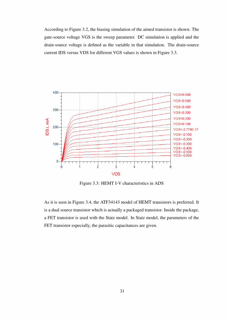
According to Figure 3.2, the biasing simulation of the aimed transistor is shown. The
gate-source voltage VGS is the sweep parameter. DC simulation is applied and the
drain-source voltage is defined as the variable in that simulation. The drain-source
current IDS versus VDS for different VGS values is shown in Figure 3.3.
Figure 3.3: HEMT I-V characteristics in ADS
As it is seen in Figure 3.4, the ATF34143 model of HEMT transistors is preferred. It
is a dual source transistor which is actually a packaged transistor. Inside the package,
a FET transistor is used with the Statz model. In Statz model, the parameters of the
FET transistor especially, the parasitic capacitances are given.
31
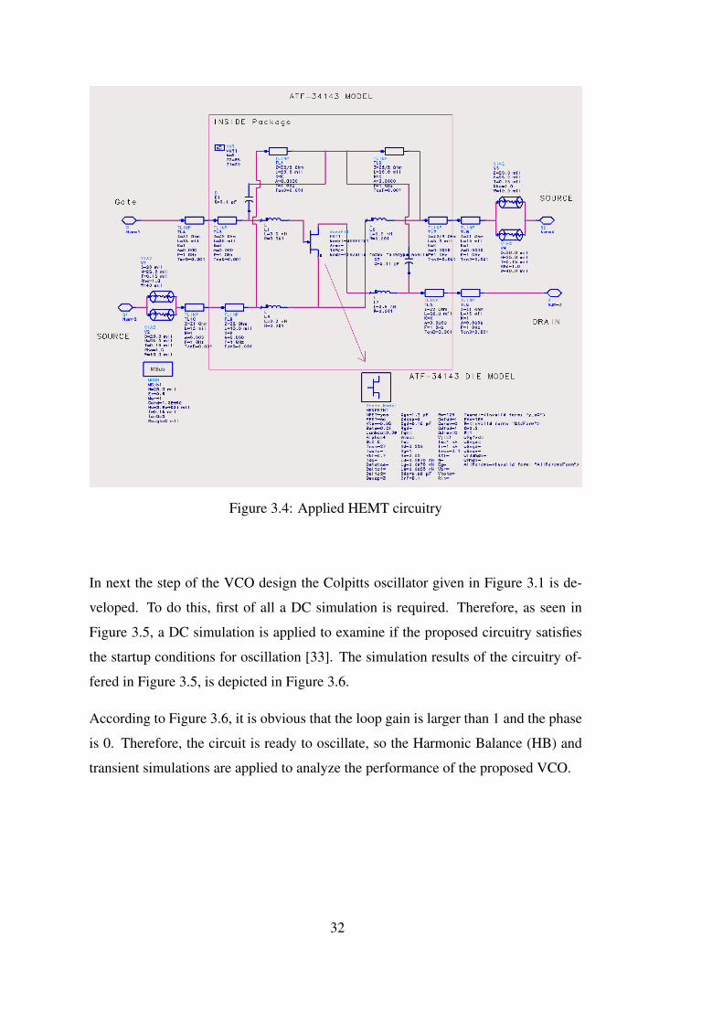
Figure 3.4: Applied HEMT circuitry
In next the step of the VCO design the Colpitts oscillator given in Figure 3.1 is de-
veloped. To do this, first of all a DC simulation is required. Therefore, as seen in
Figure 3.5, a DC simulation is applied to examine if the proposed circuitry satisfies
the startup conditions for oscillation [33]. The simulation results of the circuitry of-
fered in Figure 3.5, is depicted in Figure 3.6.
According to Figure 3.6, it is obvious that the loop gain is larger than 1 and the phase
is 0. Therefore, the circuit is ready to oscillate, so the Harmonic Balance (HB) and
transient simulations are applied to analyze the performance of the proposed VCO.
32
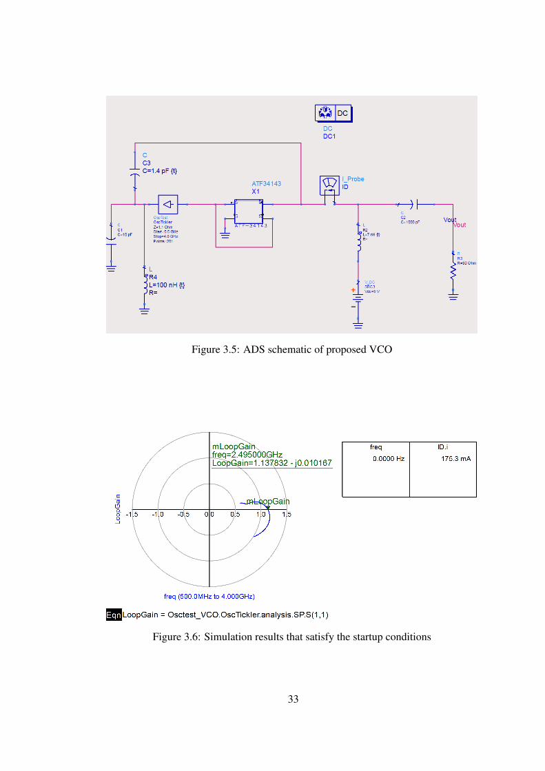
Figure 3.5: ADS schematic of proposed VCO
Figure 3.6: Simulation results that satisfy the startup conditions
33
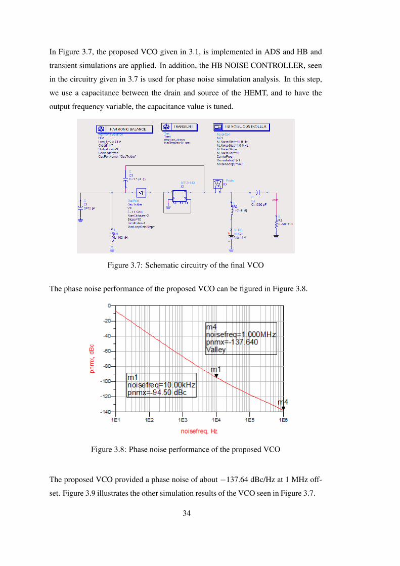
In Figure 3.7, the proposed VCO given in 3.1, is implemented in ADS and HB and
transient simulations are applied. In addition, the HB NOISE CONTROLLER, seen
in the circuitry given in 3.7 is used for phase noise simulation analysis. In this step,
we use a capacitance between the drain and source of the HEMT, and to have the
output frequency variable, the capacitance value is tuned.
Figure 3.7: Schematic circuitry of the final VCO
The phase noise performance of the proposed VCO can be figured in Figure 3.8.
Figure 3.8: Phase noise performance of the proposed VCO
The proposed VCO provided a phase noise of about −137.64 dBc/Hz at 1 MHz off-
set. Figure 3.9 illustrates the other simulation results of the VCO seen in Figure 3.7.
34
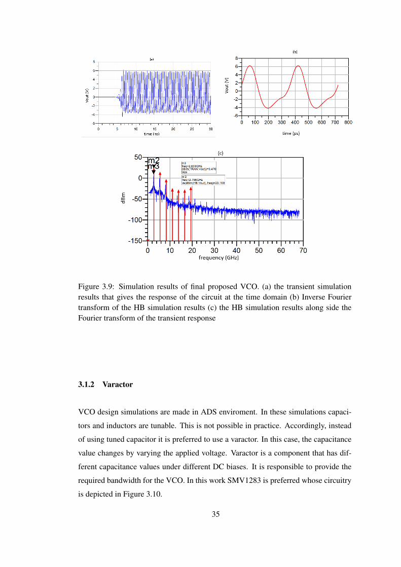
Figure 3.9: Simulation results of final proposed VCO. (a) the transient simulationresults that gives the response of the circuit at the time domain (b) Inverse Fouriertransform of the HB simulation results (c) the HB simulation results along side theFourier transform of the transient response
3.1.2 Varactor
VCO design simulations are made in ADS enviroment. In these simulations capaci-
tors and inductors are tunable. This is not possible in practice. Accordingly, instead
of using tuned capacitor it is preferred to use a varactor. In this case, the capacitance
value changes by varying the applied voltage. Varactor is a component that has dif-
ferent capacitance values under different DC biases. It is responsible to provide the
required bandwidth for the VCO. In this work SMV1283 is preferred whose circuitry
is depicted in Figure 3.10.
35
Figure 3.10: Used varactor circuitry in ADS
To generate the varactor model in ADS, using the parameters values in datasheet and
adding that values to the diode model in general circuitry of a varactor in ADS, the
model is defined. In Figure 3.11, the biasing of the given varactor is illustrated. In
addition, C-V characteristics of the applied varactor is given in Figure 3.12. In Figure
3.11, the s-parameters simulation is applied, where the Vbias value is swept as seen
in the parameter sweep section.
Figure 3.11: The varactor biasing circuitry as implemented using ADS
36
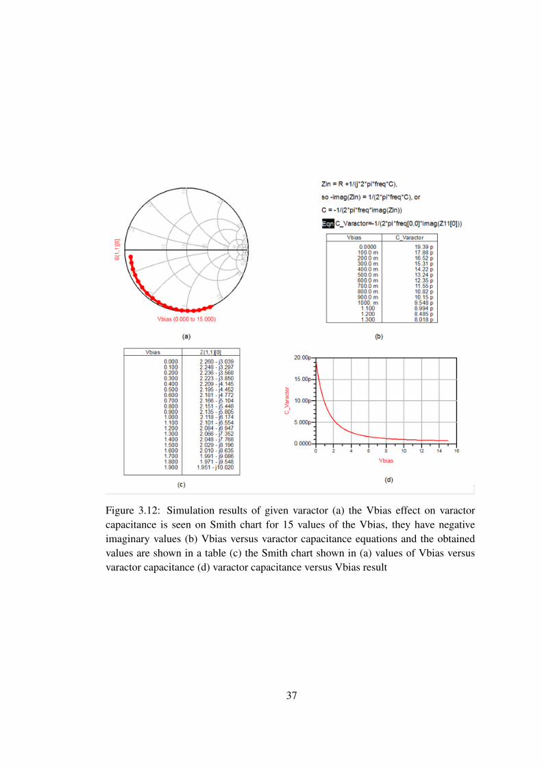
Figure 3.12: Simulation results of given varactor (a) the Vbias effect on varactorcapacitance is seen on Smith chart for 15 values of the Vbias, they have negativeimaginary values (b) Vbias versus varactor capacitance equations and the obtainedvalues are shown in a table (c) the Smith chart shown in (a) values of Vbias versusvaractor capacitance (d) varactor capacitance versus Vbias result
37
According to the simulation results shown in Figure 3.12 (d), while increasing the
Vbias value the varactor capacitance is decreased, therefore the resonance frequency
increases as shown in the following frequency expression:
f =1
2π√LC
(3.1)
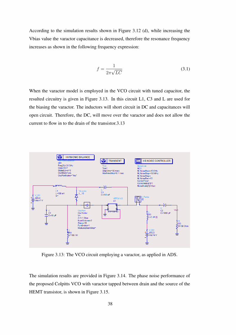
When the varactor model is employed in the VCO circuit with tuned capacitor, the
resulted circuitry is given in Figure 3.13. In this circuit L1, C3 and L are used for
the biasing the varactor. The inductors will short circuit in DC and capacitances will
open circuit. Therefore, the DC, will move over the varactor and does not allow the
current to flow in to the drain of the transistor.3.13
Figure 3.13: The VCO circuit employing a varactor, as applied in ADS.
The simulation results are provided in Figure 3.14. The phase noise performance of
the proposed Colpitts VCO with varactor tapped between drain and the source of the
HEMT transistor, is shown in Figure 3.15.
38
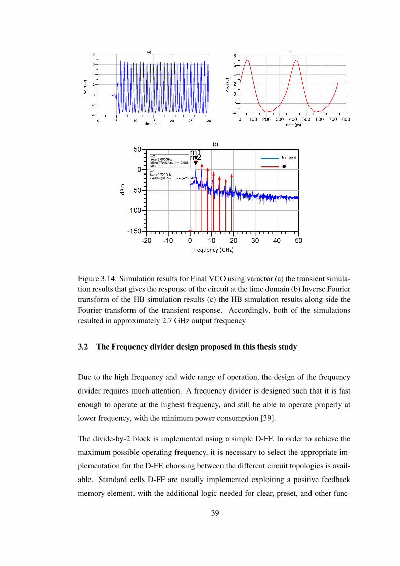
Figure 3.14: Simulation results for Final VCO using varactor (a) the transient simula-tion results that gives the response of the circuit at the time domain (b) Inverse Fouriertransform of the HB simulation results (c) the HB simulation results along side theFourier transform of the transient response. Accordingly, both of the simulationsresulted in approximately 2.7 GHz output frequency
3.2 The Frequency divider design proposed in this thesis study
Due to the high frequency and wide range of operation, the design of the frequency
divider requires much attention. A frequency divider is designed such that it is fast
enough to operate at the highest frequency, and still be able to operate properly at
lower frequency, with the minimum power consumption [39].
The divide-by-2 block is implemented using a simple D-FF. In order to achieve the
maximum possible operating frequency, it is necessary to select the appropriate im-
plementation for the D-FF, choosing between the different circuit topologies is avail-
able. Standard cells D-FF are usually implemented exploiting a positive feedback
memory element, with the additional logic needed for clear, preset, and other func-
39
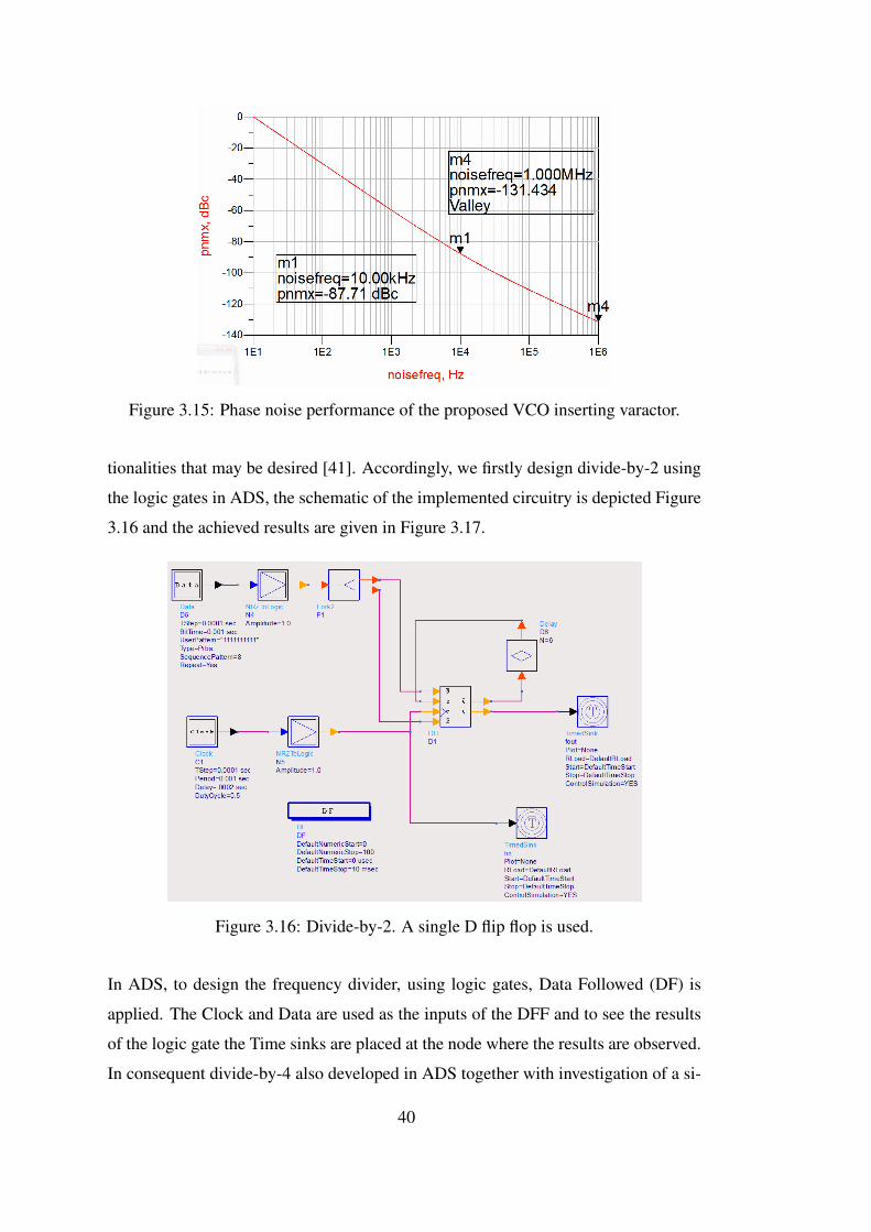
Figure 3.15: Phase noise performance of the proposed VCO inserting varactor.
tionalities that may be desired [41]. Accordingly, we firstly design divide-by-2 using
the logic gates in ADS, the schematic of the implemented circuitry is depicted Figure
3.16 and the achieved results are given in Figure 3.17.
Figure 3.16: Divide-by-2. A single D flip flop is used.
In ADS, to design the frequency divider, using logic gates, Data Followed (DF) is
applied. The Clock and Data are used as the inputs of the DFF and to see the results
of the logic gate the Time sinks are placed at the node where the results are observed.
In consequent divide-by-4 also developed in ADS together with investigation of a si-
40
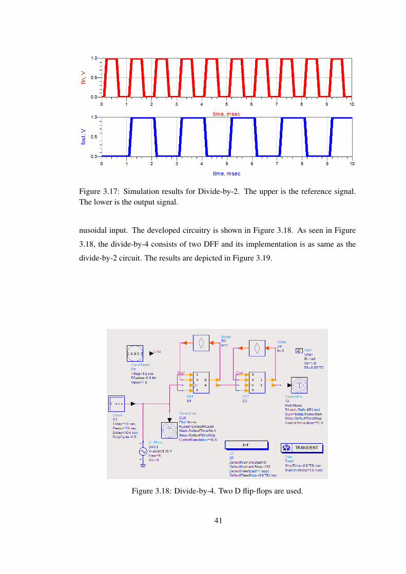
Figure 3.17: Simulation results for Divide-by-2. The upper is the reference signal.The lower is the output signal.
nusoidal input. The developed circuitry is shown in Figure 3.18. As seen in Figure
3.18, the divide-by-4 consists of two DFF and its implementation is as same as the
divide-by-2 circuit. The results are depicted in Figure 3.19.
Figure 3.18: Divide-by-4. Two D flip-flops are used.
41
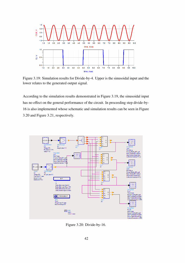
Figure 3.19: Simulation results for Divide-by-4. Upper is the sinusoidal input and thelower relates to the generated output signal.
According to the simulation results demonstrated in Figure 3.19, the sinusoidal input
has no effect on the general performance of the circuit. In proceeding step divide-by-
16 is also implemented whose schematic and simulation results can be seen in Figure
3.20 and Figure 3.21, respectively.
Figure 3.20: Divide-by-16.
42
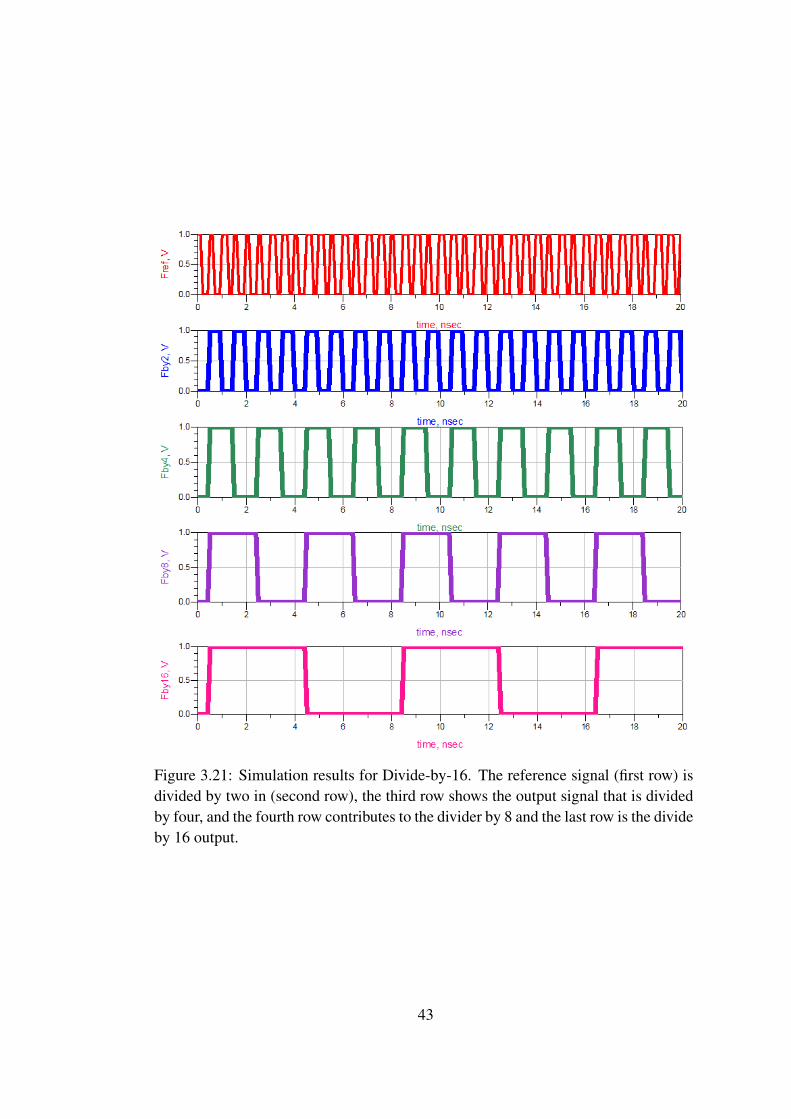
Figure 3.21: Simulation results for Divide-by-16. The reference signal (first row) isdivided by two in (second row), the third row shows the output signal that is dividedby four, and the fourth row contributes to the divider by 8 and the last row is the divideby 16 output.
43
In Figure 3.20, it is obvious that to design divide-by-16, four DFF is used. For each
D flip-flop a time sink is used at the output that shows the input, divide-by-2, divide-
by-4, divide-by-8 and finally, the divide-by-16 output signals in Figure 3.21.
During this work we had noticed that we are in need of the designing the frequency
divider in transistor level. Therefore, developing the frequency divider in transistor
level is accomplished. At beginning step a NAND gate which is depicted in Figure
3.22 is developed.
Figure 3.22: Transistor level designed NAND gate.
Figure 3.23: Simulation results for transistor level designed NAND gate. The red oneis the upper input. The blue is the lower input signal. Pink one relates to the outputof the circuit
44

The achieved results are shown in Figure 3.23. As seen in Figure 3.23, the simulation
results presents that when A=B=0 the OUT=1 and when A=B=1, the OUT=0.
In addition to two input NAND gate we were in need of three input NAND gate to
develop the DFF. Thus, a three input NAND gate that is depicted in Figure 3.24 is
implemented. The results are given in Figure 3.25.
Figure 3.24: Transistor level designed three input NAND gate.
The simulation results of the three input NAND gate, shows that if A=B=C=1 the
OUT=0 while the A=B=C=0 resulted in OUT=1. This is the behaviour of a NAND
gate. Using the provided NAND gate we can develop the conventional DFF with
added reset circuitry depicted in Figure 3.26 with results seen in Figure 3.27. When
Q2=Reset=1, the Q goes low, that is proves the behaviour of the circuit.
In Figure 3.28 a CMOS DFF, as same as the conventional DFF is implemented. Us-
ing the provided analog DFF designed frequency divider is designed. In Figure 3.29
the schematic of the designed frequency is offered and the corresponding simulation
results are shown in Figure 3.30.
45
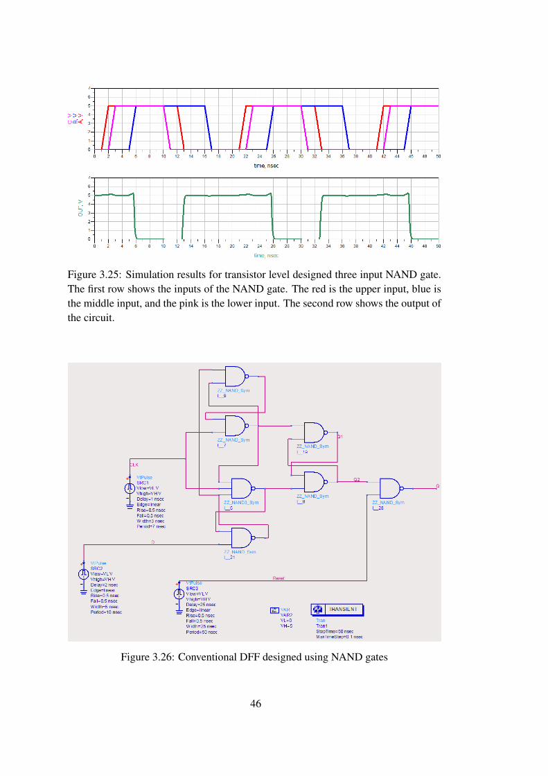
Figure 3.25: Simulation results for transistor level designed three input NAND gate.The first row shows the inputs of the NAND gate. The red is the upper input, blue isthe middle input, and the pink is the lower input. The second row shows the output ofthe circuit.
Figure 3.26: Conventional DFF designed using NAND gates
46
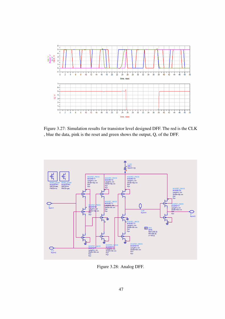
Figure 3.27: Simulation results for transistor level designed DFF. The red is the CLK, blue the data, pink is the reset and green shows the output, Q, of the DFF.
Figure 3.28: Analog DFF.
47
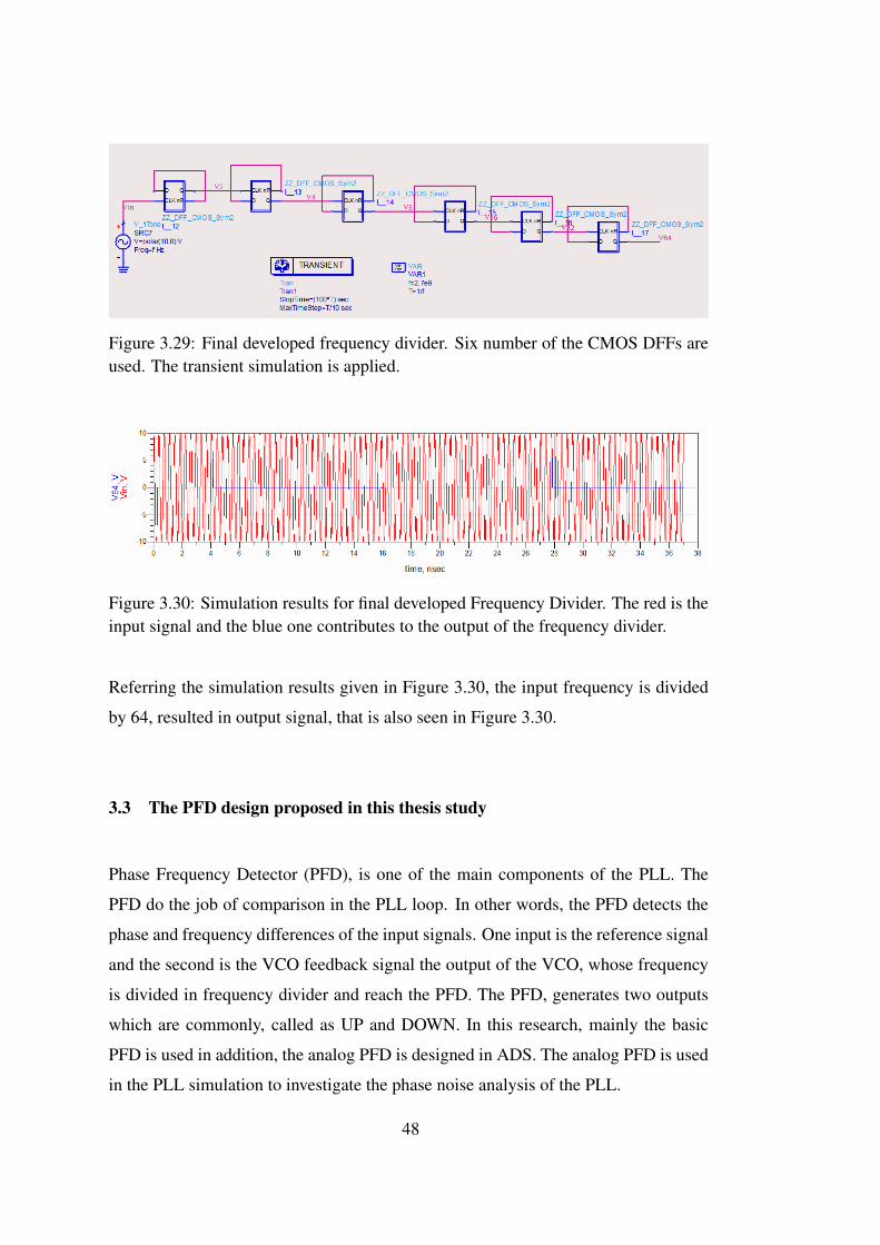
Figure 3.29: Final developed frequency divider. Six number of the CMOS DFFs areused. The transient simulation is applied.
Figure 3.30: Simulation results for final developed Frequency Divider. The red is theinput signal and the blue one contributes to the output of the frequency divider.
Referring the simulation results given in Figure 3.30, the input frequency is divided
by 64, resulted in output signal, that is also seen in Figure 3.30.
3.3 The PFD design proposed in this thesis study
Phase Frequency Detector (PFD), is one of the main components of the PLL. The
PFD do the job of comparison in the PLL loop. In other words, the PFD detects the
phase and frequency differences of the input signals. One input is the reference signal
and the second is the VCO feedback signal the output of the VCO, whose frequency
is divided in frequency divider and reach the PFD. The PFD, generates two outputs
which are commonly, called as UP and DOWN. In this research, mainly the basic
PFD is used in addition, the analog PFD is designed in ADS. The analog PFD is used
in the PLL simulation to investigate the phase noise analysis of the PLL.
48
3.3.1 Basic PFD
The basic PFD, is the most commonly preferred PFD in the PLL applications. There-
fore in this thesis study we firstly implemented the basic PFD, that is discussed in
chapter 2 with detailed. Therefore, in this section the developed basic PFD with ob-
tained results are presented.
Figure 3.31: ADS schematic of Basic PFD, composed of two DFF and one NANDgate, with DF simulation and Time sinks to generate the simulation results
To implement the basic PFD in ADS as in Figure 3.31, the DF (Data Fallowed) simu-
lation is used. The timing diagram of it can be offered such as depicted in Figure 3.32.
Referring to the Figure 3.31, Signal CLK arrives at the DFF1, made the output ‘UP’
high (This state will be remained until CLK is clocked high again). DFF2 receives
CLK2 made ’DOWN’ high. Then, NAND gate will receive two ones as it’s inputs.
A low output that is the clear to the DFFs caused the DFFs to reset with CLK and
CLK2 and became low. A ‘pulse’ out of DOWN will be seen as DOWN only went
high when CLK2 was high but was immediately reset due to the NAND.
49
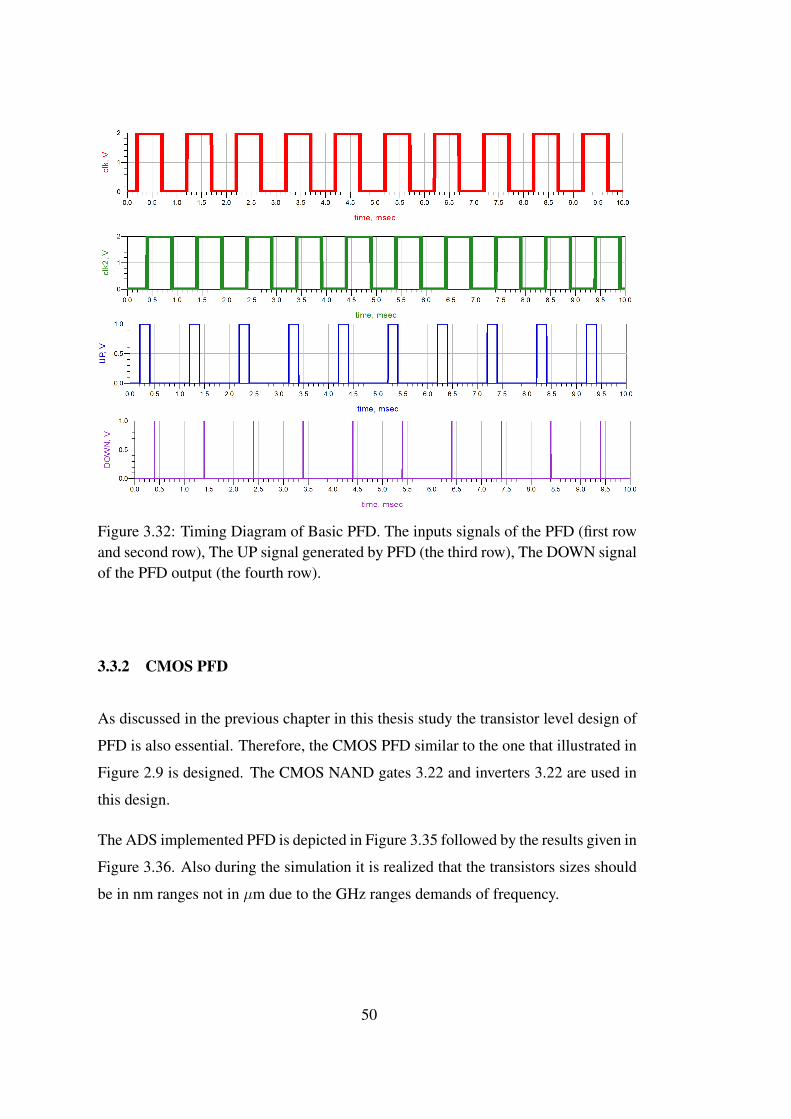
Figure 3.32: Timing Diagram of Basic PFD. The inputs signals of the PFD (first rowand second row), The UP signal generated by PFD (the third row), The DOWN signalof the PFD output (the fourth row).
3.3.2 CMOS PFD
As discussed in the previous chapter in this thesis study the transistor level design of
PFD is also essential. Therefore, the CMOS PFD similar to the one that illustrated in
Figure 2.9 is designed. The CMOS NAND gates 3.22 and inverters 3.22 are used in
this design.
The ADS implemented PFD is depicted in Figure 3.35 followed by the results given in
Figure 3.36. Also during the simulation it is realized that the transistors sizes should
be in nm ranges not in µm due to the GHz ranges demands of frequency.
50
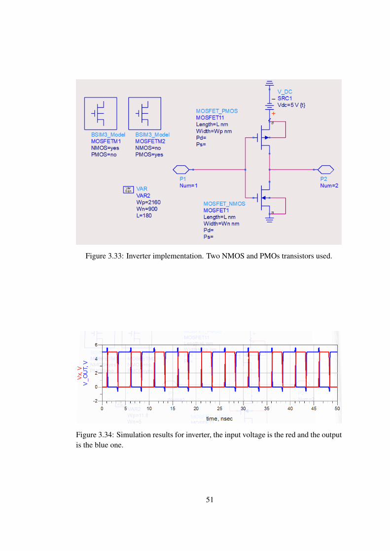
Figure 3.33: Inverter implementation. Two NMOS and PMOs transistors used.
Figure 3.34: Simulation results for inverter, the input voltage is the red and the outputis the blue one.
51
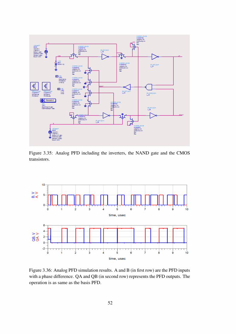
Figure 3.35: Analog PFD including the inverters, the NAND gate and the CMOStransistors.
Figure 3.36: Analog PFD simulation results. A and B (in first row) are the PFD inputswith a phase difference. QA and QB (in second row) represents the PFD outputs. Theoperation is as same as the basis PFD.
52
The designed CMOS PFD performance is as we expected. The main goal of designing
the CP is to produce two output signals of UP and DOWN or QA and QB. These QA
and QB voltages are used to open the switches of the CP. The switches should not
be opened at the same time. When one is on, the other should be off. The obtained
results in Figure 3.36 are proved this behaviour. Consequently, in the PLL design it
will be used.
3.4 The Charge pump and loop filter design proposed in this thesis study
In this research to develop the basic charge pump which is depicted in Figure 2.10, a
charge pump using NMOS and PMOS transistors is designed. The ADS implemen-
tation of the investigated CP is presented in Figure 3.37.
As a comparison to the basic charge pump given in Figure 2.10, in the charge pump
illustrated in Figure 3.37, we use NMOS and PMOS transistors for switches and the
current sources. Moreover, a switch is added to the circuit before the loop filter. The
reason of it can be explained as, the transient analysis of the charge pump needed
the place of the switch before the loop filter as the capacitor shorted at t=0 which
discharged the capacitor and when t>0, it will be opened. The simulation results of
the offered charge pump is depicted in Figure 3.38.
53
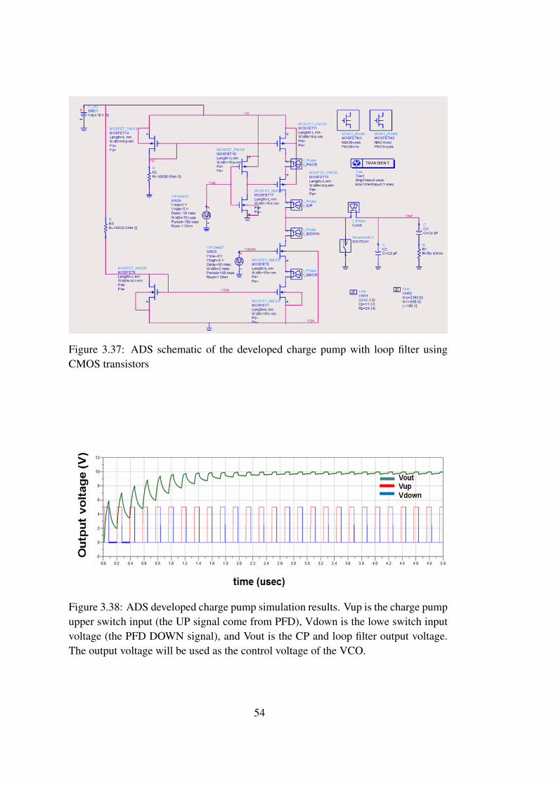
Figure 3.37: ADS schematic of the developed charge pump with loop filter usingCMOS transistors
Figure 3.38: ADS developed charge pump simulation results. Vup is the charge pumpupper switch input (the UP signal come from PFD), Vdown is the lowe switch inputvoltage (the PFD DOWN signal), and Vout is the CP and loop filter output voltage.The output voltage will be used as the control voltage of the VCO.
54

3.4.1 Charge pump design summary
In this section a summary of the provided charge pump will be offered. As a start-
ing point the relationships for NMOS and PMOS transistors currents are given in
equations 3.2 and 3.4, respectively:
IDn =1
2µnCox(
W
L)(VGS − Vth)2 (3.2)
IDp =1
2µpCox(
W
L)(VGS−|Vth|)2 (3.3)
Where Vth=0.7 V, Kn=1
2µnCox and Kp=
1
2µpCox
To continue the design the biasing of the transistors should be noted. Accordingly,
the biasing of the PMOS transistor is offered in Figure 3.39.
Figure 3.39: PMOS transistor biasing in ADS
The biasing simulation results are given in Figure 3.40.
55
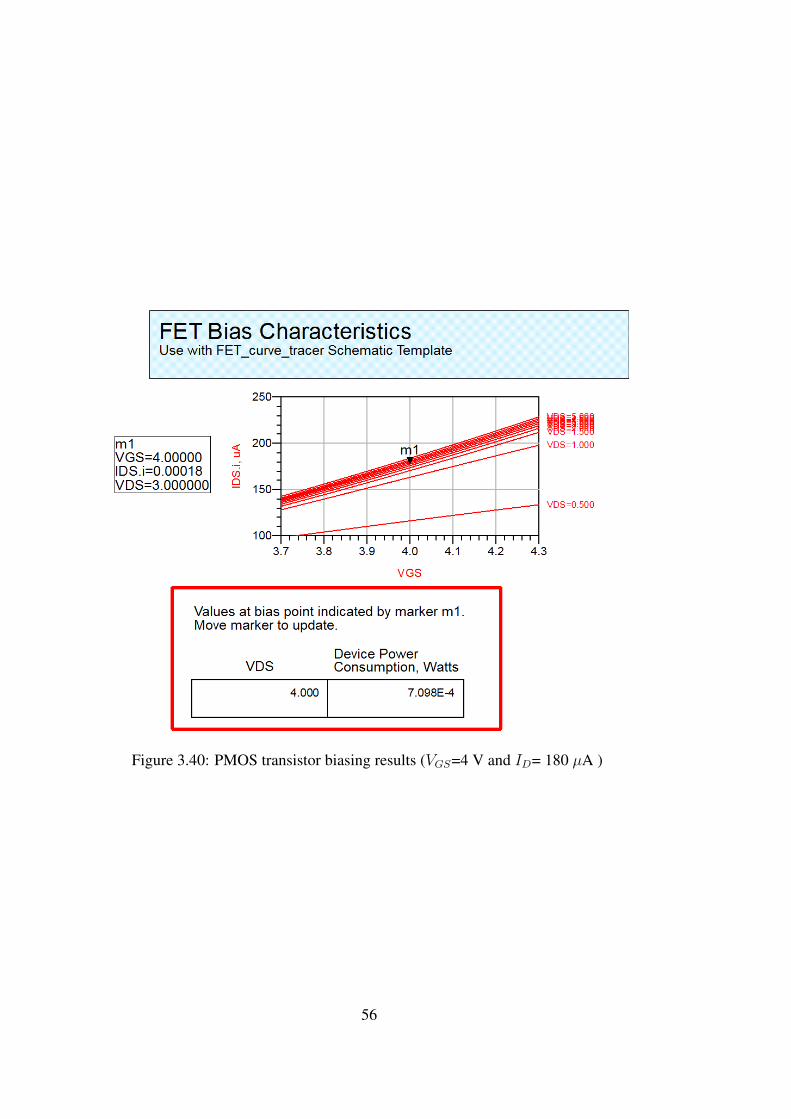
Figure 3.40: PMOS transistor biasing results (VGS=4 V and ID= 180 µA )
56
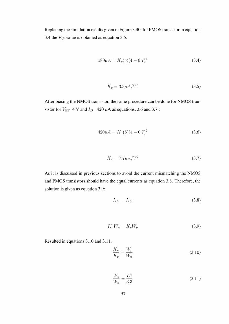
Replacing the simulation results given in Figure 3.40, for PMOS transistor in equation
3.4 the KP value is obtained as equation 3.5:
180µA = Kp(5)(4− 0.7)2 (3.4)
Kp = 3.3µA/V 2 (3.5)
After biasing the NMOS transistor, the same procedure can be done for NMOS tran-
sistor for VGS=4 V and ID= 420 µA as equations, 3.6 and 3.7 :
420µA = Kn(5)(4− 0.7)2 (3.6)
Kn = 7.7µA/V 2 (3.7)
As it is discussed in previous sections to avoid the current mismatching the NMOS
and PMOS transistors should have the equal currents as equation 3.8. Therefore, the
solution is given as equation 3.9:
IDn = IDp (3.8)
KnWn = KpWp (3.9)
Resulted in equations 3.10 and 3.11,
Kn
Kp
=Wp
Wn
(3.10)
Wp
Wn
=7.7
3.3(3.11)
57
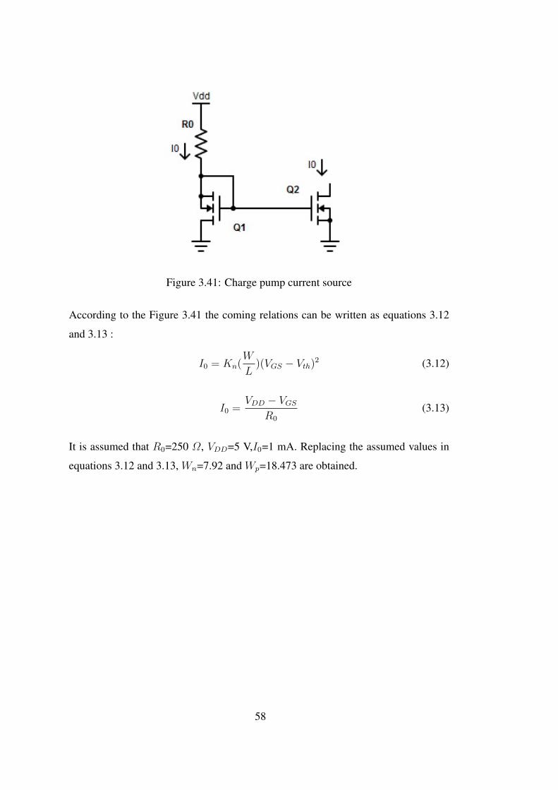
Figure 3.41: Charge pump current source
According to the Figure 3.41 the coming relations can be written as equations 3.12
and 3.13 :
I0 = Kn(W
L)(VGS − Vth)2 (3.12)
I0 =VDD − VGS
R0
(3.13)
It is assumed that R0=250 Ω, VDD=5 V,I0=1 mA. Replacing the assumed values in
equations 3.12 and 3.13, Wn=7.92 and Wp=18.473 are obtained.
58
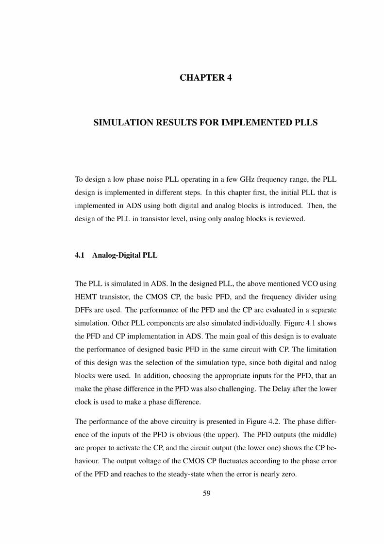
CHAPTER 4
SIMULATION RESULTS FOR IMPLEMENTED PLLS
To design a low phase noise PLL operating in a few GHz frequency range, the PLL
design is implemented in different steps. In this chapter first, the initial PLL that is
implemented in ADS using both digital and analog blocks is introduced. Then, the
design of the PLL in transistor level, using only analog blocks is reviewed.
4.1 Analog-Digital PLL
The PLL is simulated in ADS. In the designed PLL, the above mentioned VCO using
HEMT transistor, the CMOS CP, the basic PFD, and the frequency divider using
DFFs are used. The performance of the PFD and the CP are evaluated in a separate
simulation. Other PLL components are also simulated individually. Figure 4.1 shows
the PFD and CP implementation in ADS. The main goal of this design is to evaluate
the performance of designed basic PFD in the same circuit with CP. The limitation
of this design was the selection of the simulation type, since both digital and nalog
blocks were used. In addition, choosing the appropriate inputs for the PFD, that an
make the phase difference in the PFD was also challenging. The Delay after the lower
clock is used to make a phase difference.
The performance of the above circuitry is presented in Figure 4.2. The phase differ-
ence of the inputs of the PFD is obvious (the upper). The PFD outputs (the middle)
are proper to activate the CP, and the circuit output (the lower one) shows the CP be-
haviour. The output voltage of the CMOS CP fluctuates according to the phase error
of the PFD and reaches to the steady-state when the error is nearly zero.
59
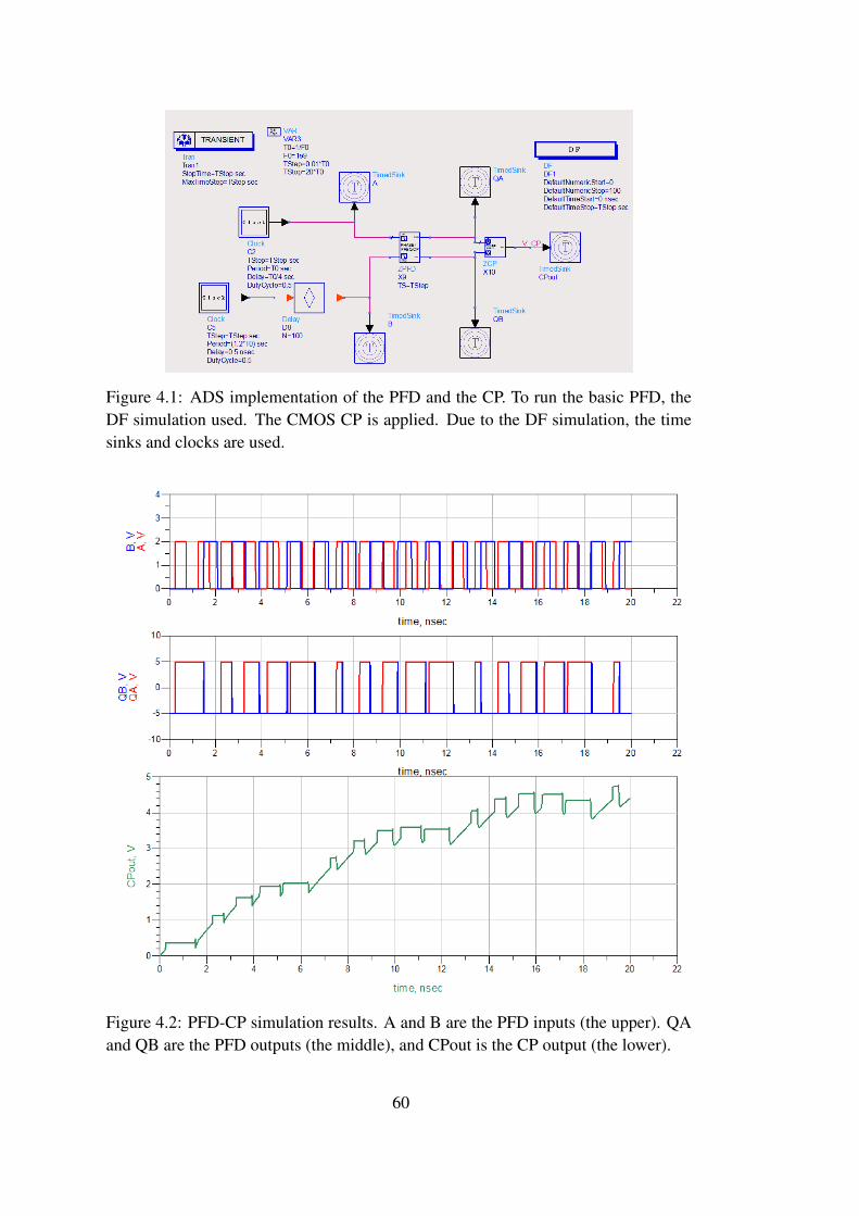
Figure 4.1: ADS implementation of the PFD and the CP. To run the basic PFD, theDF simulation used. The CMOS CP is applied. Due to the DF simulation, the timesinks and clocks are used.
Figure 4.2: PFD-CP simulation results. A and B are the PFD inputs (the upper). QAand QB are the PFD outputs (the middle), and CPout is the CP output (the lower).
60
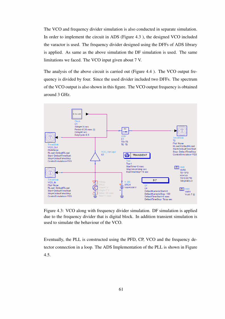
The VCO and frequency divider simulation is also conducted in separate simulation.
In order to implement the circuit in ADS (Figure 4.3 ), the designed VCO included
the varactor is used. The frequency divider designed using the DFFs of ADS library
is applied. As same as the above simulation the DF simulation is used. The same
limitations we faced. The VCO input given about 7 V.
The analysis of the above circuit is carried out (Figure 4.4 ). The VCO output fre-
quency is divided by four. Since the used divider included two DFFs. The spectrum
of the VCO output is also shown in this figure. The VCO output frequency is obtained
around 3 GHz.
Figure 4.3: VCO along with frequency divider simulation. DF simulation is applieddue to the frequency divider that is digital block. In addition transient simulation isused to simulate the behaviour of the VCO.
Eventually, the PLL is constructed using the PFD, CP, VCO and the frequency de-
tector connection in a loop. The ADS Implementation of the PLL is shown in Figure
4.5.
61
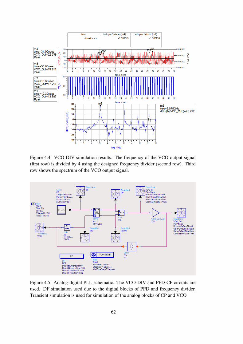
Figure 4.4: VCO-DIV simulation results. The frequency of the VCO output signal(first row) is divided by 4 using the designed frequency divider (second row). Thirdrow shows the spectrum of the VCO output signal.
Figure 4.5: Analog-digital PLL schematic. The VCO-DIV and PFD-CP circuits areused. DF simulation used due to the digital blocks of PFD and frequency divider.Transient simulation is used for simulation of the analog blocks of CP and VCO
62
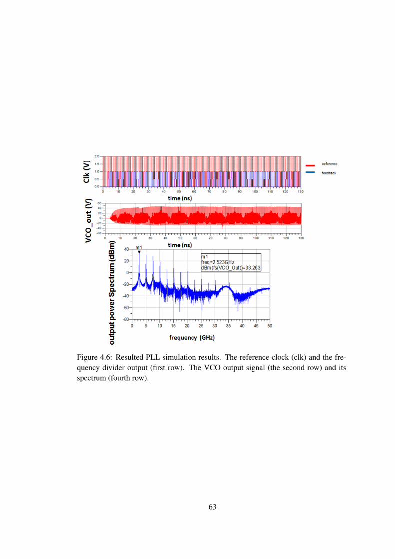
Figure 4.6: Resulted PLL simulation results. The reference clock (clk) and the fre-quency divider output (first row). The VCO output signal (the second row) and itsspectrum (fourth row).
63
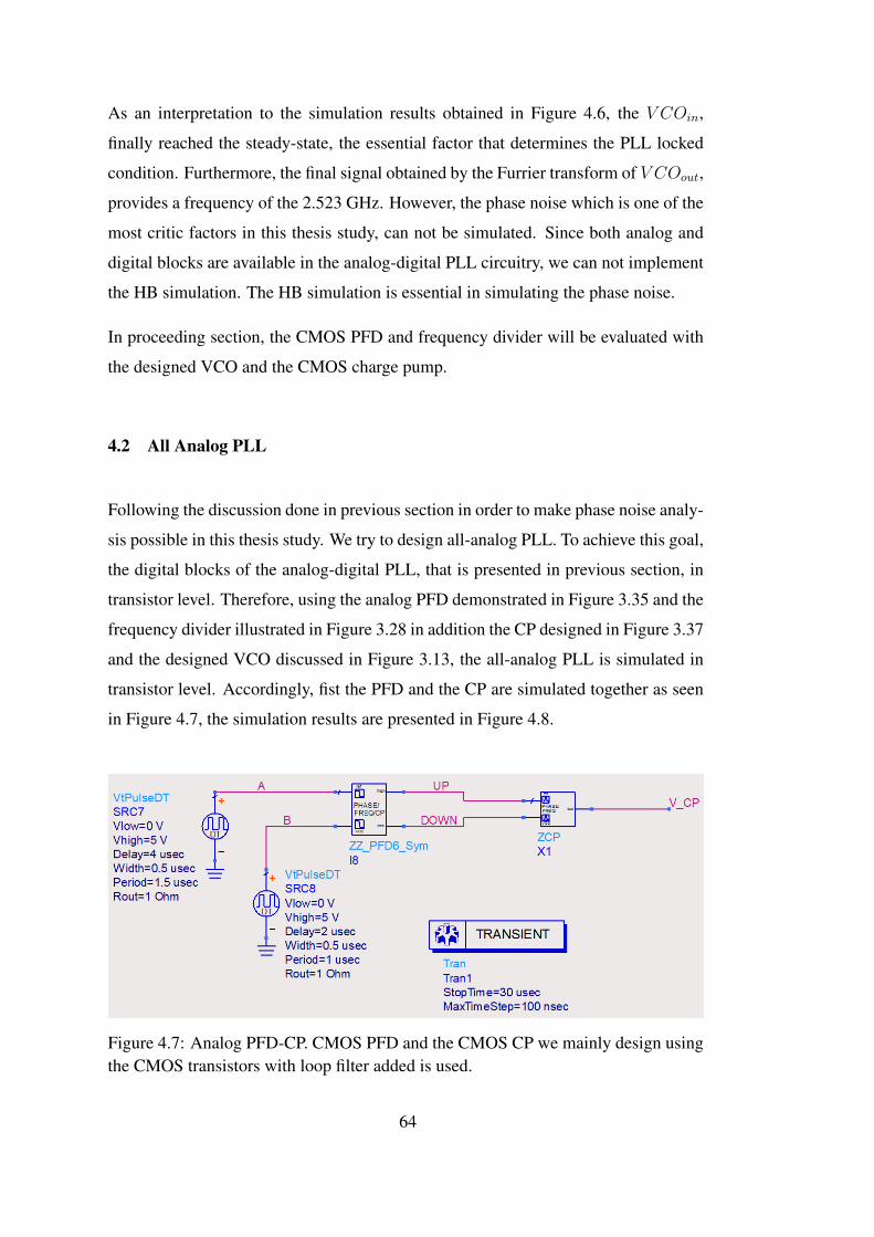
As an interpretation to the simulation results obtained in Figure 4.6, the V COin,
finally reached the steady-state, the essential factor that determines the PLL locked
condition. Furthermore, the final signal obtained by the Furrier transform of V COout,
provides a frequency of the 2.523 GHz. However, the phase noise which is one of the
most critic factors in this thesis study, can not be simulated. Since both analog and
digital blocks are available in the analog-digital PLL circuitry, we can not implement
the HB simulation. The HB simulation is essential in simulating the phase noise.
In proceeding section, the CMOS PFD and frequency divider will be evaluated with
the designed VCO and the CMOS charge pump.
4.2 All Analog PLL
Following the discussion done in previous section in order to make phase noise analy-
sis possible in this thesis study. We try to design all-analog PLL. To achieve this goal,
the digital blocks of the analog-digital PLL, that is presented in previous section, in
transistor level. Therefore, using the analog PFD demonstrated in Figure 3.35 and the
frequency divider illustrated in Figure 3.28 in addition the CP designed in Figure 3.37
and the designed VCO discussed in Figure 3.13, the all-analog PLL is simulated in
transistor level. Accordingly, fist the PFD and the CP are simulated together as seen
in Figure 4.7, the simulation results are presented in Figure 4.8.
Figure 4.7: Analog PFD-CP. CMOS PFD and the CMOS CP we mainly design usingthe CMOS transistors with loop filter added is used.
64
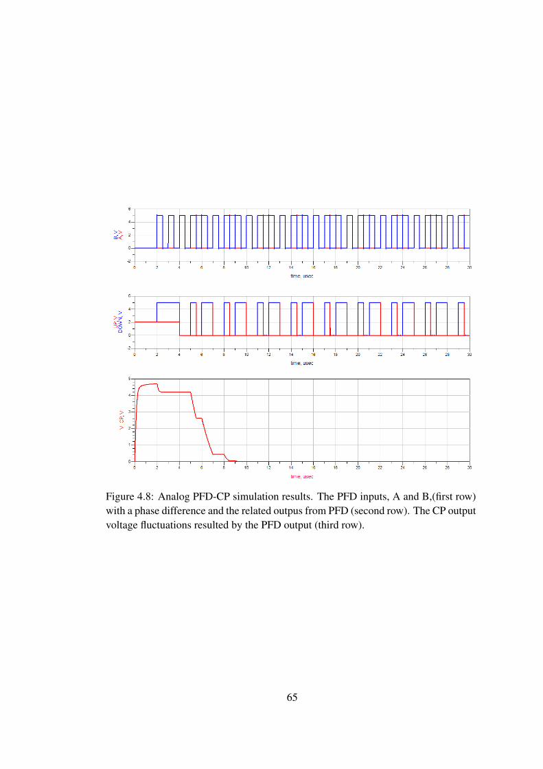
Figure 4.8: Analog PFD-CP simulation results. The PFD inputs, A and B,(first row)with a phase difference and the related outpus from PFD (second row). The CP outputvoltage fluctuations resulted by the PFD output (third row).
65
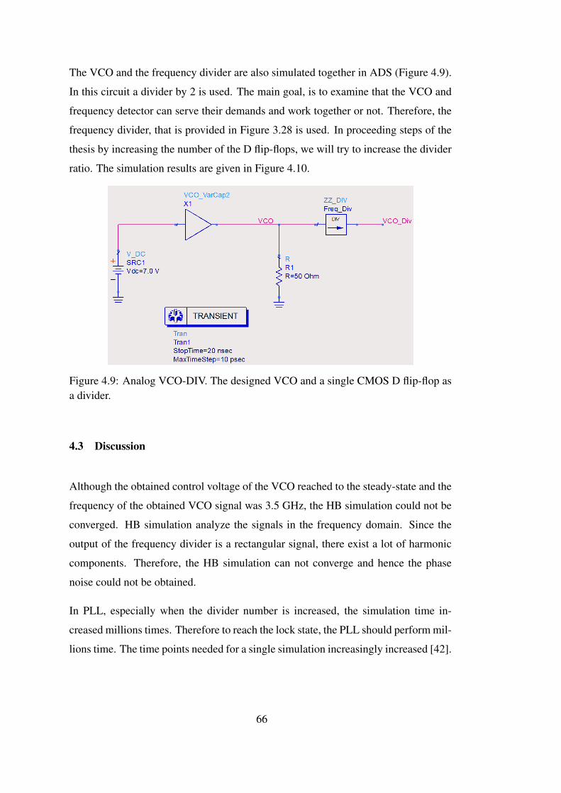
The VCO and the frequency divider are also simulated together in ADS (Figure 4.9).
In this circuit a divider by 2 is used. The main goal, is to examine that the VCO and
frequency detector can serve their demands and work together or not. Therefore, the
frequency divider, that is provided in Figure 3.28 is used. In proceeding steps of the
thesis by increasing the number of the D flip-flops, we will try to increase the divider
ratio. The simulation results are given in Figure 4.10.
Figure 4.9: Analog VCO-DIV. The designed VCO and a single CMOS D flip-flop asa divider.
4.3 Discussion
Although the obtained control voltage of the VCO reached to the steady-state and the
frequency of the obtained VCO signal was 3.5 GHz, the HB simulation could not be
converged. HB simulation analyze the signals in the frequency domain. Since the
output of the frequency divider is a rectangular signal, there exist a lot of harmonic
components. Therefore, the HB simulation can not converge and hence the phase
noise could not be obtained.
In PLL, especially when the divider number is increased, the simulation time in-
creased millions times. Therefore to reach the lock state, the PLL should perform mil-
lions time. The time points needed for a single simulation increasingly increased [42].
66
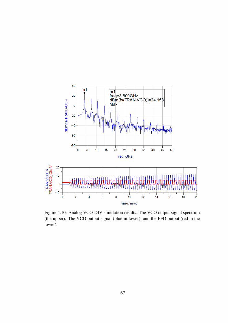
Figure 4.10: Analog VCO-DIV simulation results. The VCO output signal spectrum(the upper). The VCO output signal (blue in lower), and the PFD output (red in thelower).
67

68
CHAPTER 5
PLL PHASE NOISE ANALYSIS
The closed-loop PLL noise is an important factor of the total system performance in
modern digital communications which use phase modulation. The PLL noise model
includes the effect of the blocks forming the PLL as well as the VCO [43]. In section
??, the phase noise basics are reviewed. In this chapter the PLL noise analysis will be
illustrated in detail. First, using the loop dynamics studied in section 2.2.2, analytical
methods will be discussed. Then, using the analytical results, the phase noise analysis
of the CPPLL, will be done in ADS.
5.1 PLL Noise Analysis
Phase noise of a VCO placed inside a PLL is shaped by the PLL noise transfer func-
tions [43]. A free running VCO phase noise is simply called VCO phase noise while
the phase noise of a VCO inside a locked PLL is called PLL output phase noise. The
overall PLL output phase noise is characterized by the noise contributions of all the
blocks in a PLL [43]. In Figure 5.1 the PLL noise model that is preferred in this thesis
study is shown.
According to the noise model that is shown in Figure 5.1, in this study the PFD
and CP noises are modelled together, the VCO and frequency divider noises are also
modelled.
69
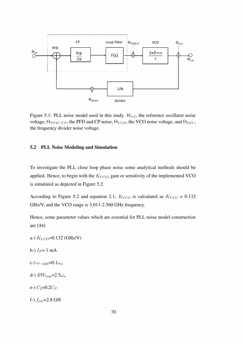
Figure 5.1: PLL noise model used in this study. Θref , the reference oscillator noisevoltage, ΘPFD−CP , the PFD and CP noise, ΘV CO, the VCO noise voltage, and ΘDIV ,the frequency divider noise voltage.
5.2 PLL Noise Modeling and Simulation
To investigate the PLL close loop phase noise some analytical methods should be
applied. Hence, to begin with the KV CO, gain or sensitivity of the implemented VCO
is simulated as depicted in Figure 5.2.
According to Figure 5.2 and equation 2.1, KV CO is calculated as KV CO = 0.132
GHz/V, and the VCO range is 3.011-2.560 GHz frequency.
Hence, some parameter values which are essential for PLL noise model construction
are [44]
a-) KV CO=0.132 (GHz/V)
b-) IP= 1 mA
c-) ω−3dB=0.1ωn
d-) BWloop=2.5ωn
e-) C2=0.2CP
f-) fout=2.8 GH
70
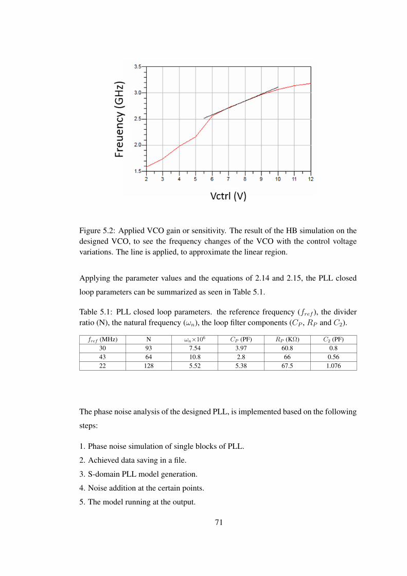
Figure 5.2: Applied VCO gain or sensitivity. The result of the HB simulation on thedesigned VCO, to see the frequency changes of the VCO with the control voltagevariations. The line is applied, to approximate the linear region.
Applying the parameter values and the equations of 2.14 and 2.15, the PLL closed
loop parameters can be summarized as seen in Table 5.1.
Table 5.1: PLL closed loop parameters. the reference frequency (fref ), the dividerratio (N), the natural frequency (ωn), the loop filter components (CP , RP and C2).
fref (MHz) N ωn×106 CP (PF) RP (KΩ) C2 (PF)30 93 7.54 3.97 60.8 0.843 64 10.8 2.8 66 0.5622 128 5.52 5.38 67.5 1.076
The phase noise analysis of the designed PLL, is implemented based on the following
steps:
1. Phase noise simulation of single blocks of PLL.
2. Achieved data saving in a file.
3. S-domain PLL model generation.
4. Noise addition at the certain points.
5. The model running at the output.
71
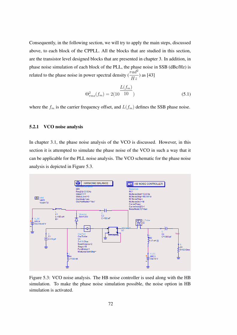
Consequently, in the following section, we will try to apply the main steps, discussed
above, to each block of the CPPLL. All the blocks that are studied in this section,
are the transistor level designed blocks that are presented in chapter 3. In addition, in
phase noise simulation of each block of the PLL, the phase noise in SSB (dBc/Hz) is
related to the phase noise in power spectral density (rad2
Hz) as [43]
Θ2rms(fm) = 2(10
L(fm)
10 ) (5.1)
where the fm is the carrier frequency offset, and L(fm) defines the SSB phase noise.
5.2.1 VCO noise analysis
In chapter 3.1, the phase noise analysis of the VCO is discussed. However, in this
section it is attempted to simulate the phase noise of the VCO in such a way that it
can be applicable for the PLL noise analysis. The VCO schematic for the phase noise
analysis is depicted in Figure 5.3.
Figure 5.3: VCO noise analysis. The HB noise controller is used along with the HBsimulation. To make the phase noise simulation possible, the noise option in HBsimulation is activated.
72
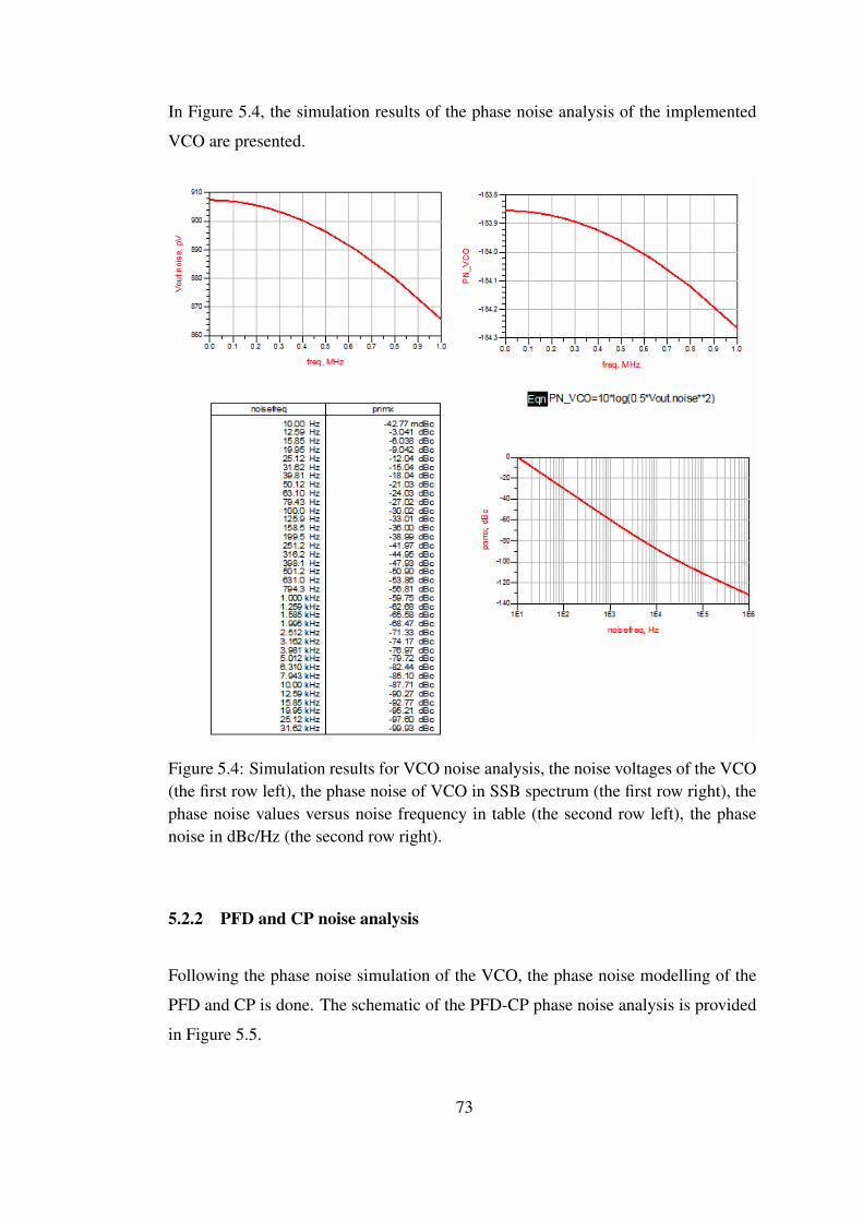
In Figure 5.4, the simulation results of the phase noise analysis of the implemented
VCO are presented.
Figure 5.4: Simulation results for VCO noise analysis, the noise voltages of the VCO(the first row left), the phase noise of VCO in SSB spectrum (the first row right), thephase noise values versus noise frequency in table (the second row left), the phasenoise in dBc/Hz (the second row right).
5.2.2 PFD and CP noise analysis
Following the phase noise simulation of the VCO, the phase noise modelling of the
PFD and CP is done. The schematic of the PFD-CP phase noise analysis is provided
in Figure 5.5.
73
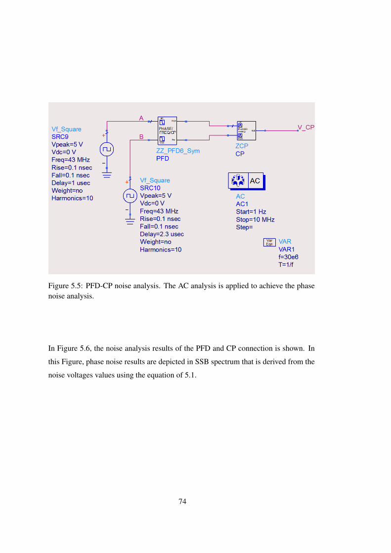
Figure 5.5: PFD-CP noise analysis. The AC analysis is applied to achieve the phasenoise analysis.
In Figure 5.6, the noise analysis results of the PFD and CP connection is shown. In
this Figure, phase noise results are depicted in SSB spectrum that is derived from the
noise voltages values using the equation of 5.1.
74
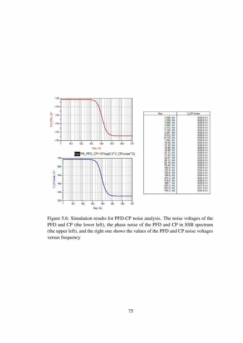
Figure 5.6: Simulation results for PFD-CP noise analysis. The noise voltages of thePFD and CP (the lower left), the phase noise of the PFD and CP in SSB spectrum(the upper left), and the right one shows the values of the PFD and CP noise voltagesversus frequency
75
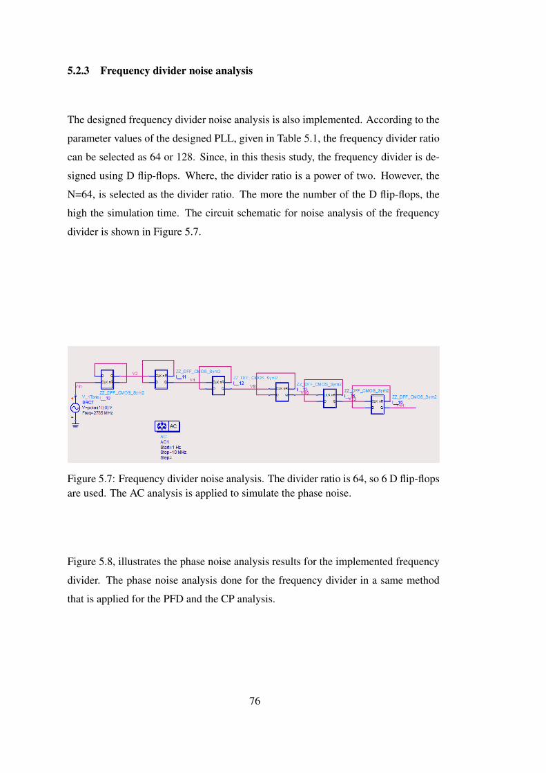
5.2.3 Frequency divider noise analysis
The designed frequency divider noise analysis is also implemented. According to the
parameter values of the designed PLL, given in Table 5.1, the frequency divider ratio
can be selected as 64 or 128. Since, in this thesis study, the frequency divider is de-
signed using D flip-flops. Where, the divider ratio is a power of two. However, the
N=64, is selected as the divider ratio. The more the number of the D flip-flops, the
high the simulation time. The circuit schematic for noise analysis of the frequency
divider is shown in Figure 5.7.
Figure 5.7: Frequency divider noise analysis. The divider ratio is 64, so 6 D flip-flopsare used. The AC analysis is applied to simulate the phase noise.
Figure 5.8, illustrates the phase noise analysis results for the implemented frequency
divider. The phase noise analysis done for the frequency divider in a same method
that is applied for the PFD and the CP analysis.
76
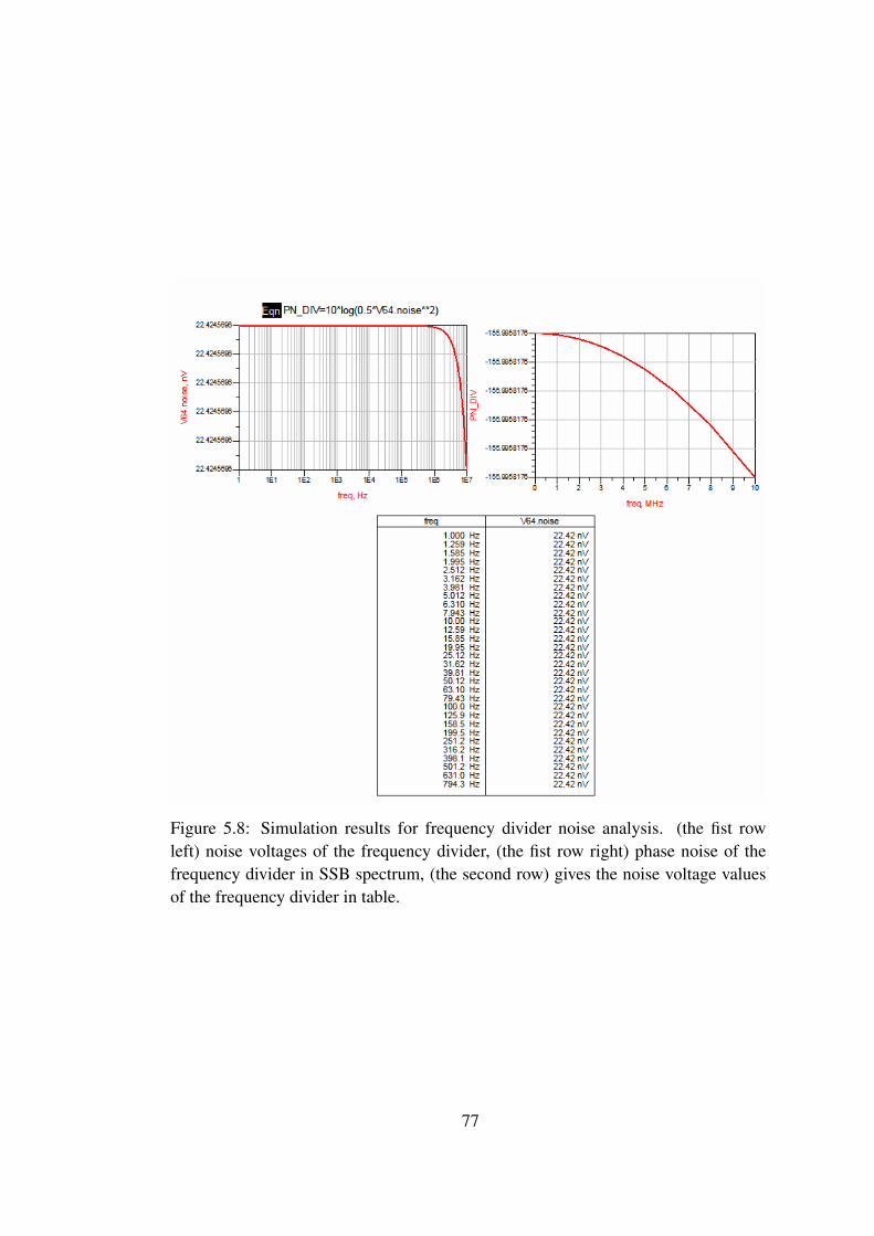
Figure 5.8: Simulation results for frequency divider noise analysis. (the fist rowleft) noise voltages of the frequency divider, (the fist row right) phase noise of thefrequency divider in SSB spectrum, (the second row) gives the noise voltage valuesof the frequency divider in table.
77
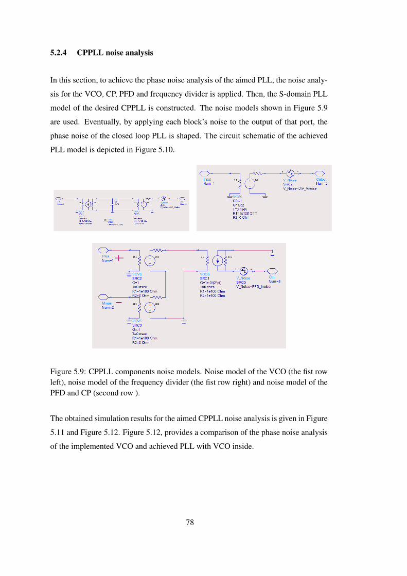
5.2.4 CPPLL noise analysis
In this section, to achieve the phase noise analysis of the aimed PLL, the noise analy-
sis for the VCO, CP, PFD and frequency divider is applied. Then, the S-domain PLL
model of the desired CPPLL is constructed. The noise models shown in Figure 5.9
are used. Eventually, by applying each block’s noise to the output of that port, the
phase noise of the closed loop PLL is shaped. The circuit schematic of the achieved
PLL model is depicted in Figure 5.10.
Figure 5.9: CPPLL components noise models. Noise model of the VCO (the fist rowleft), noise model of the frequency divider (the fist row right) and noise model of thePFD and CP (second row ).
The obtained simulation results for the aimed CPPLL noise analysis is given in Figure
5.11 and Figure 5.12. Figure 5.12, provides a comparison of the phase noise analysis
of the implemented VCO and achieved PLL with VCO inside.
78
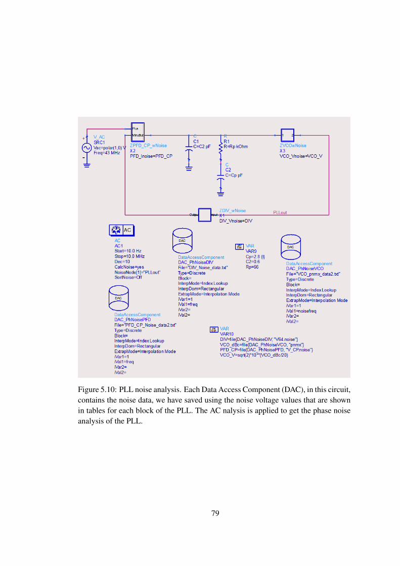
Figure 5.10: PLL noise analysis. Each Data Access Component (DAC), in this circuit,contains the noise data, we have saved using the noise voltage values that are shownin tables for each block of the PLL. The AC nalysis is applied to get the phase noiseanalysis of the PLL.
79
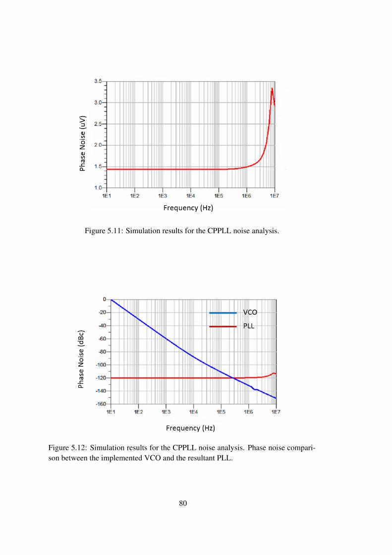
Figure 5.11: Simulation results for the CPPLL noise analysis.
Figure 5.12: Simulation results for the CPPLL noise analysis. Phase noise compari-son between the implemented VCO and the resultant PLL.
80
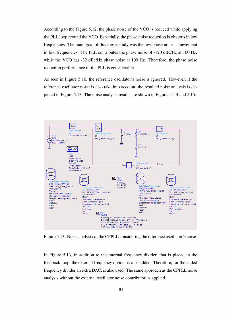
According to the Figure 5.12, the phase noise of the VCO is reduced while applying
the PLL loop around the VCO. Especially, the phase noise reduction is obvious in low
frequencies. The main goal of this thesis study was the low phase noise achievement
in low frequencies. The PLL contributes the phase noise of -120 dBc/Hz at 100 Hz,
while the VCO has -32 dBc/Hz phase noise at 100 Hz. Therefore, the phase noise
reduction performance of the PLL is considerable.
As seen in Figure 5.10, the reference oscillator’s noise is ignored. However, if the
reference oscillator noise is also take into account, the resulted noise analysis is de-
picted in Figure 5.13. The noise analysis results are shown in Figures 5.14 and 5.15.
Figure 5.13: Noise analysis of the CPPLL considering the reference oscillator’s noise.
In Figure 5.13, in addition to the internal frequency divider, that is placed in the
feedback loop, the external frequency divider is also added. Therefore, for the added
frequency divider an extra DAC, is also used. The same approach as the CPPLL noise
analysis without the external oscillator noise contributor, is applied.
81
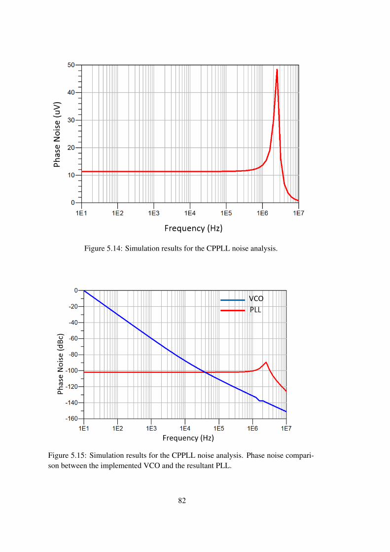
Figure 5.14: Simulation results for the CPPLL noise analysis.
Figure 5.15: Simulation results for the CPPLL noise analysis. Phase noise compari-son between the implemented VCO and the resultant PLL.
82
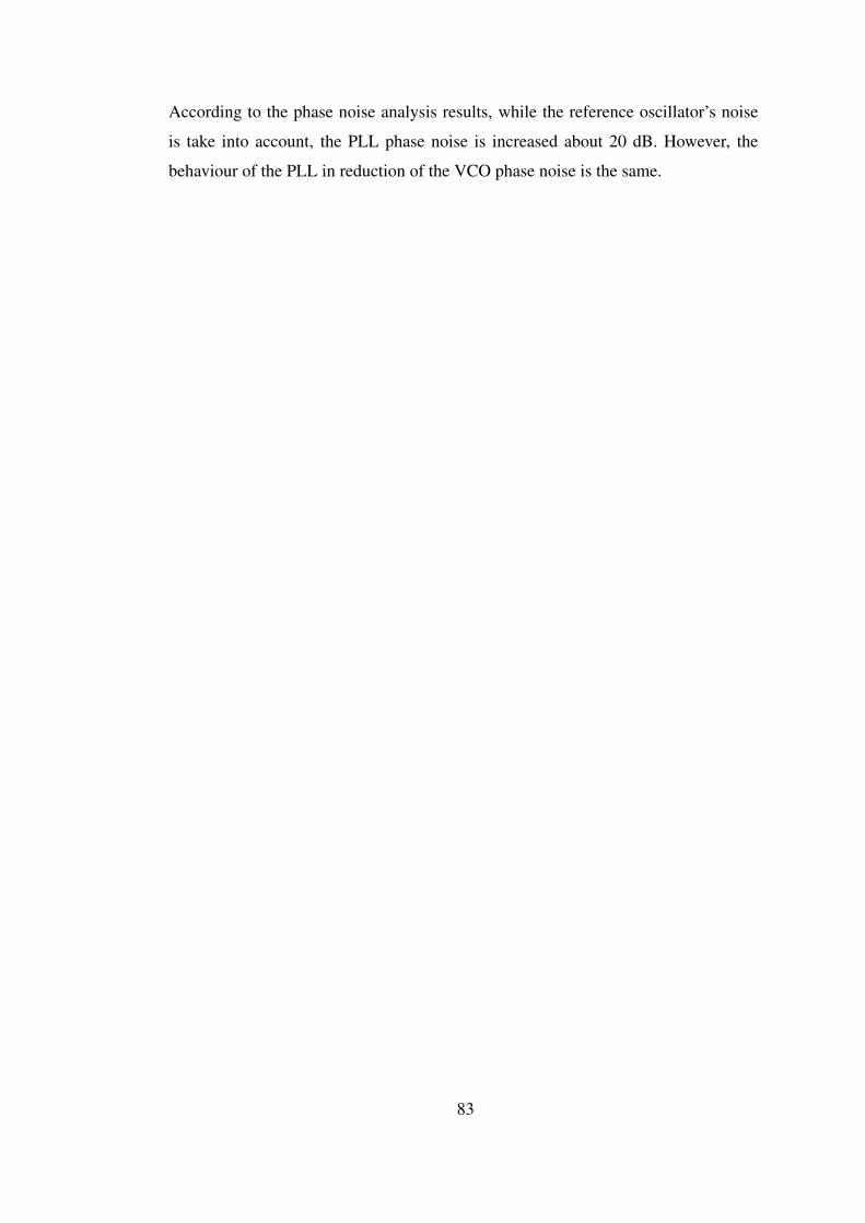
According to the phase noise analysis results, while the reference oscillator’s noise
is take into account, the PLL phase noise is increased about 20 dB. However, the
behaviour of the PLL in reduction of the VCO phase noise is the same.
83

84
CHAPTER 6
CONCLUSION AND FUTURE WORK
In this thesis study, the design of a low phase noise CPPLL at 2.8 GHz for the mi-
crowave transmitter of the HMMDI, is presented. In HMMDI method, a microwave
signal (a few GHz) is transmitted to the vibrating tissue (as a result of ultrasound
excitation). The backscattered signal consists of a signal at the carrier frequency
(operating microwave frequency) and a signal at vibration frequency (Doppler fre-
quency). The vibration frequency is in the range of a few Hz. To realize this signal,
the phase noise of the transmitter should be low.
A Phase locked Loop (PLL) as a circuit block to decrease the phase noise is selected.
Different building blocks of the PLL including the VCO, frequency divider, PFD,
CP and loop filter are designed using ADS. A gate grounding Colpittes VCO using
HEMT transistor is designed. HEMT transistor is preferred because it has low noise
figure and it can operate at high microwave frequencies. The Colpittes VCO is de-
signed using capacitor and varactor. In the capacitor version, the capacitor is tuned
manually but in the varactor version, the capacitance changes by varying the applied
voltage. Using the capacitor, the obtained phase noise is -137.64 dBc/Hz at 1 MHz
and using the varactor it is -131.434 dBc/Hz. The simulated VCO provides an oscil-
lating frequency of around 2.7 GHz.
To bring the output frequency of the VCO to MHz frequency range provided by the
external crystal oscillator (reference signal) a frequency divider is used. The fre-
quency divider is simulated first using the D flip-flop blocks of the ADS and then by
the analog D flip-flop designed by the CMOS transistors. The CMOS D flip-flops are
preferred to simulate the phase noise of the PLL.
85
Commonly used PFD in PLL applications (basic PFD) was designed to detect the
phase differences of the reference signal and the VCO output after passing through
the frequency divider. Since HB simulation can not be run for phase noise analysis
while using built-in blocks of ADS in the DSP library, the analog PFD is designed
in transistor level using CMOS transistors. The phase noise of the PLL is simulated
using this type of PFD.
To generate the control voltage for the VCO, a CP followed by a loop filter is consid-
ered. The output voltage of the CMOS CP fluctuates according to the phase error of
the PFD and reaches to the steady-state when the error is nearly zero.
The PLL is simulated in ADS. In the designed PLL, the above mentioned VCO using
HEMT transistor, the CMOS CP, the basic PFD, and the frequency divider using
DFFs are used. The performance of the PFD and the CP are evaluated in a separate
simulation. Other PLL components are also simulated individually.
Although the obtained control voltage of the VCO reached to the steady-state and the
frequency of the obtained VCO signal was 3.5 GHz, the HB simulation could not be
converged. HB simulation analyze the signals in the frequency domain. Since the
output of the frequency divider is a rectangular signal, there exist a lot of harmonic
components. Therefore, the HB simulation can not converge and hence the phase
noise could not be obtained.
In order to analyze the phase noise. PLL is linearised and the parameters of each
block were analytically calculated. For each block of the PLL loop the phase noise
was simulated. The S-domain PLL model was generated. The loop was closed after
adding the noise at specific points. Assuming noiseless crystal oscillator, the phase
noise was -120 dBc/Hz at 100 Hz offset. The phase noise was decreased successfully
90 dBc compared to the VCO phase noise (-32 dBc/Hz at 100 Hz). While the noise
of crystal oscillator is included, the phase noise at 100 Hz reached to -101 dBc/Hz.
The results show that the PLL loop method has a potential of decreasing the phase
noise of the oscillator.
In the future work the following studies can be performed:
86
The phase noise of the designed VCO can be improved. Other VCO topologies using
CMOS transistors can be designed. The resonator tank with high Q (Quality factor)
can be used,
In frequency divider design the dual modulus dividers can be examined. The fre-
quency divider can be designed programmable leading to fractional PLL frequency
synthesizers,
Alternative PFDs including the latch based PFD, MPTPFD, and Falling-Edge PFD
can be designed,
In the CP design, applying a differential CP can be useful. The CMFB circuitry will
also be added to the loop filter in differential CP design,
All the implementations in this thesis are conducted in schematic level. The stud-
ied PLL is simulated using the CMOS transistor models in standard libraries of ADS
except the VCO that is designed using a single HEMT transistor. In future the inves-
tigated PLL can be implemented in IBM 7RF SOI process.
87

88
REFERENCES
[1] B. Razavi, Monolithic phase-locked loops and clock recovery circuits: theoryand design. John Wiley & Sons, 1996.
[2] B. Razavi, RF Microelectronics. Upper Saddle River, NJ, USA: Prentice-Hall,Inc., 1998.
[3] M. Mansuri, D. Liu, and C.-K. Yang, “Fast frequency acquisition phase-frequency detectors for gsa/s phase-locked loops,” in Solid-State Circuits Con-ference, 2001. ESSCIRC 2001. Proceedings of the 27th European, pp. 333–336,Sept 2001.
[4] B. Terlemez, Oscillation control in CMOS phase-locked loops. PhD thesis, Cite-seer, 2004.
[5] C. B. Top, Harmonic Motion Microwave Doppler Imaging Method. Thesis,2013.
[6] C. Top and N. Gencer, “Harmonic motion microwave doppler imaging: A simu-lation study using a simple breast model,” Medical Imaging, IEEE Transactionson, vol. 33, pp. 290–300, Feb 2014.
[7] C. A. A. Viana et al., “Injected phototransistor oscillator,” 2010.
[8] H. de Bellescize, La reception synchrone. E. Chiron, 1932.
[9] Z. Fu, J. Lee, and A. Apsel, “A 6.8ghz low-power and low-phase-noise phase-locked loop design,” in Circuits and Systems, 2008. ISCAS 2008. IEEE Interna-tional Symposium on, pp. 1732–1735, May 2008.
[10] R. Bondare, C. Dethe, D. Bhoyar, and M. Mushrif, “Design of high frequencyphase locked loop,” in Communication Control and Computing Technologies(ICCCCT), 2010 IEEE International Conference on, pp. 586–591, Oct 2010.
[11] A. Seli, H. Nguyen, L. He, and M. Jones, “Capacitor free phase locked loop de-sign in 45nm,” in Quality Electronic Design (ISQED), 2011 12th InternationalSymposium on, pp. 1–6, March 2011.
[12] M. Yogesh, M. Dietl, P. Sareen, and K. Dewan, “A low power, self-biased, band-width tracking semi-digital pll design,” in Electronics Design, Systems and Ap-plications (ICEDSA), 2012 IEEE International Conference on, pp. 135–140,Nov 2012.
89
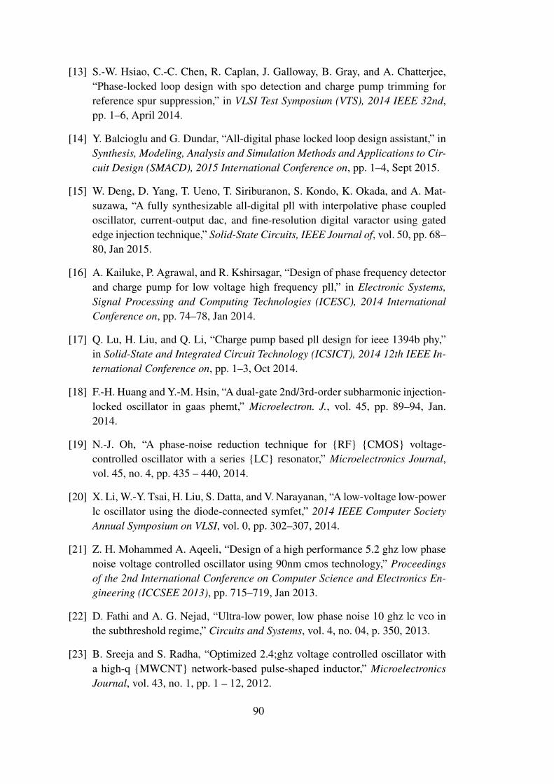
[13] S.-W. Hsiao, C.-C. Chen, R. Caplan, J. Galloway, B. Gray, and A. Chatterjee,“Phase-locked loop design with spo detection and charge pump trimming forreference spur suppression,” in VLSI Test Symposium (VTS), 2014 IEEE 32nd,pp. 1–6, April 2014.
[14] Y. Balcioglu and G. Dundar, “All-digital phase locked loop design assistant,” inSynthesis, Modeling, Analysis and Simulation Methods and Applications to Cir-cuit Design (SMACD), 2015 International Conference on, pp. 1–4, Sept 2015.
[15] W. Deng, D. Yang, T. Ueno, T. Siriburanon, S. Kondo, K. Okada, and A. Mat-suzawa, “A fully synthesizable all-digital pll with interpolative phase coupledoscillator, current-output dac, and fine-resolution digital varactor using gatededge injection technique,” Solid-State Circuits, IEEE Journal of, vol. 50, pp. 68–80, Jan 2015.
[16] A. Kailuke, P. Agrawal, and R. Kshirsagar, “Design of phase frequency detectorand charge pump for low voltage high frequency pll,” in Electronic Systems,Signal Processing and Computing Technologies (ICESC), 2014 InternationalConference on, pp. 74–78, Jan 2014.
[17] Q. Lu, H. Liu, and Q. Li, “Charge pump based pll design for ieee 1394b phy,”in Solid-State and Integrated Circuit Technology (ICSICT), 2014 12th IEEE In-ternational Conference on, pp. 1–3, Oct 2014.
[18] F.-H. Huang and Y.-M. Hsin, “A dual-gate 2nd/3rd-order subharmonic injection-locked oscillator in gaas phemt,” Microelectron. J., vol. 45, pp. 89–94, Jan.2014.
[19] N.-J. Oh, “A phase-noise reduction technique for RF CMOS voltage-controlled oscillator with a series LC resonator,” Microelectronics Journal,vol. 45, no. 4, pp. 435 – 440, 2014.
[20] X. Li, W.-Y. Tsai, H. Liu, S. Datta, and V. Narayanan, “A low-voltage low-powerlc oscillator using the diode-connected symfet,” 2014 IEEE Computer SocietyAnnual Symposium on VLSI, vol. 0, pp. 302–307, 2014.
[21] Z. H. Mohammed A. Aqeeli, “Design of a high performance 5.2 ghz low phasenoise voltage controlled oscillator using 90nm cmos technology,” Proceedingsof the 2nd International Conference on Computer Science and Electronics En-gineering (ICCSEE 2013), pp. 715–719, Jan 2013.
[22] D. Fathi and A. G. Nejad, “Ultra-low power, low phase noise 10 ghz lc vco inthe subthreshold regime,” Circuits and Systems, vol. 4, no. 04, p. 350, 2013.
[23] B. Sreeja and S. Radha, “Optimized 2.4;ghz voltage controlled oscillator witha high-q MWCNT network-based pulse-shaped inductor,” MicroelectronicsJournal, vol. 43, no. 1, pp. 1 – 12, 2012.
90
[24] Y. Liu, “Reliability analysis of MOS varactor in CMOS LC VCO,”Microelectronics Journal, vol. 42, no. 2, pp. 330 – 333, 2011.
[25] J. C. Nunez-Perez, J. Verdier, and C. Gontrand, “Design of 20ghz high per-formance lc-vcos in a 52ghz ft sige: C bicmos technology,” Microelectron. J.,vol. 41, pp. 41–50, Jan. 2010.
[26] N.-J. Oh and S.-G. Lee, “Current reused lc vcos,” Microwave and Wireless Com-ponents Letters, IEEE, vol. 15, pp. 736–738, Nov 2005.
[27] D. Ham and A. Hajimiri, “Concepts and methods in optimization of integratedlc vcos,” Solid-State Circuits, IEEE Journal of, vol. 36, pp. 896–909, Jun 2001.
[28] J. J. Fitzpatrick, Analysis and Design of Low-Jitter Oscillators. PhD thesis,Citeseer, 2004.
[29] A. Khattoi, A non-sequential phase detector for low jitter clock recovery appli-cations. PhD thesis, Kansas State University, 2010.
[30] N. M. H. Ismail and M. Othman, “Cmos phase frequency detector for highspeed applications,” in Design and Test Workshop (IDT), 2009 4th International,pp. 1–5, IEEE, 2009.
[31] K. Arshak, O. Abubaker, and E. Jafer, “Design and simulation difference typescmos phase frequency detector for high speed and low jitter pll,” in Devices, Cir-cuits and Systems, 2004. Proceedings of the Fifth IEEE International CaracasConference on, vol. 1, pp. 188–191, IEEE, 2004.
[32] G. Lee, P. Chan, and L. Siek, “A cmos phase frequency detector for charge pumpphase-locked loop,” in Circuits and Systems, 1999. 42nd Midwest Symposiumon, vol. 2, pp. 601–604 vol. 2, 1999.
[33] B. Razavi, RF Microelectronics (2Nd Edition) (Prentice Hall CommunicationsEngineering and Emerging Technologies Series). Upper Saddle River, NJ, USA:Prentice Hall Press, 2nd ed., 2011.
[34] P. S. Stetson, “Design considerations for low phase jitter clock generators,” tech.rep., DTIC Document, 1998.
[35] L. Zhiqun, Z. Shuangshuang, and H. Ningbing, “Design of a high performancecmos charge pump for phase-locked loop synthesizers,” Journal of Semiconduc-tors, vol. 32, no. 7, p. 075007, 2011.
[36] N. Nouri and S. Mirabbasi, “A900mhz-2ghz low-swing low-power 0.18/splmu/m cmos pll,” in Electrical and Computer Engineering, 2005. Canadian Con-ference on, pp. 1566–1569, May 2005.
91
[37] H. Djahanshahi and C. A. T. Salama, “Differential cmos circuits for 622-mhz/933-mhz clock and data recovery applications,” Solid-State Circuits, IEEEJournal of, vol. 35, no. 6, pp. 847–855, 2000.
[38] W. Rhee, “Design of high-performance cmos charge pumps in phase-lockedloops,” in Circuits and Systems, 1999. ISCAS’99. Proceedings of the 1999 IEEEInternational Symposium on, vol. 2, pp. 545–548, IEEE, 1999.
[39] B. C. Chye, Novel Techniques for Fully Integrated RF CMOS Phase-LockedLoop Frequency Synthesizer. PhD thesis, Nanyang Technological University,2004.
[40] R. Ratan, Design of a phase locked loop based clocking circuit for high speed se-rial link applications. PhD thesis, University of Illinois at Urbana-Champaign,2014.
[41] F. Barale, “Frequency dividers design for multi-ghz pll systems,” 2008.
[42] K. Kundert, “Predicting the phase noise of pll-based frequency synthesizers,”2002.
[43] A. Aktas and M. Ismail, CMOS PLLs and VCOs for 4G Wireless. SpringerPublishing Company, Incorporated, 2013.
[44] B. Razavi, “Introduction to PLLs.” http://www.seas.ucla.edu/brweb/teaching/215C_W2013/PLLs.pdf, 2000.
92


![DESIGN AND ANALYSIS OF EFFICIENT PHASE LOCKED LOOP … · Phase Locked Loop (PLL) mainly for synchronization, clock synthesis, skew and jitter reduction [5]. Phase locked loops find](https://img.pdfslide.us/doc/110x75/5e9d540ca2a49a4e746bfacd/design-and-analysis-of-efficient-phase-locked-loop-phase-locked-loop-pll-mainly.jpg)