Embed Size (px)
Citation preview
© 2010 Renesas Electronics Corporation. All rights reserved. 00000-A
Oct. 20th 2010
Common EDA Platform Development Dept.
Rev. 1.00
Renesas Electronics Corporation
Koji Hirakimoto
A Strategy of PowerA Strategy of Power--Intent Based Design Flow Intent Based Design Flow in Renesas Electronics in Renesas Electronics
2 © 2010 Renesas Electronics Corporation. All rights reserved.
Outline
Corporate Overview
Current Issues on MSMV Design Flow
Our Proposed Solutions
Summary

3 © 2010 Renesas Electronics Corporation. All rights reserved.
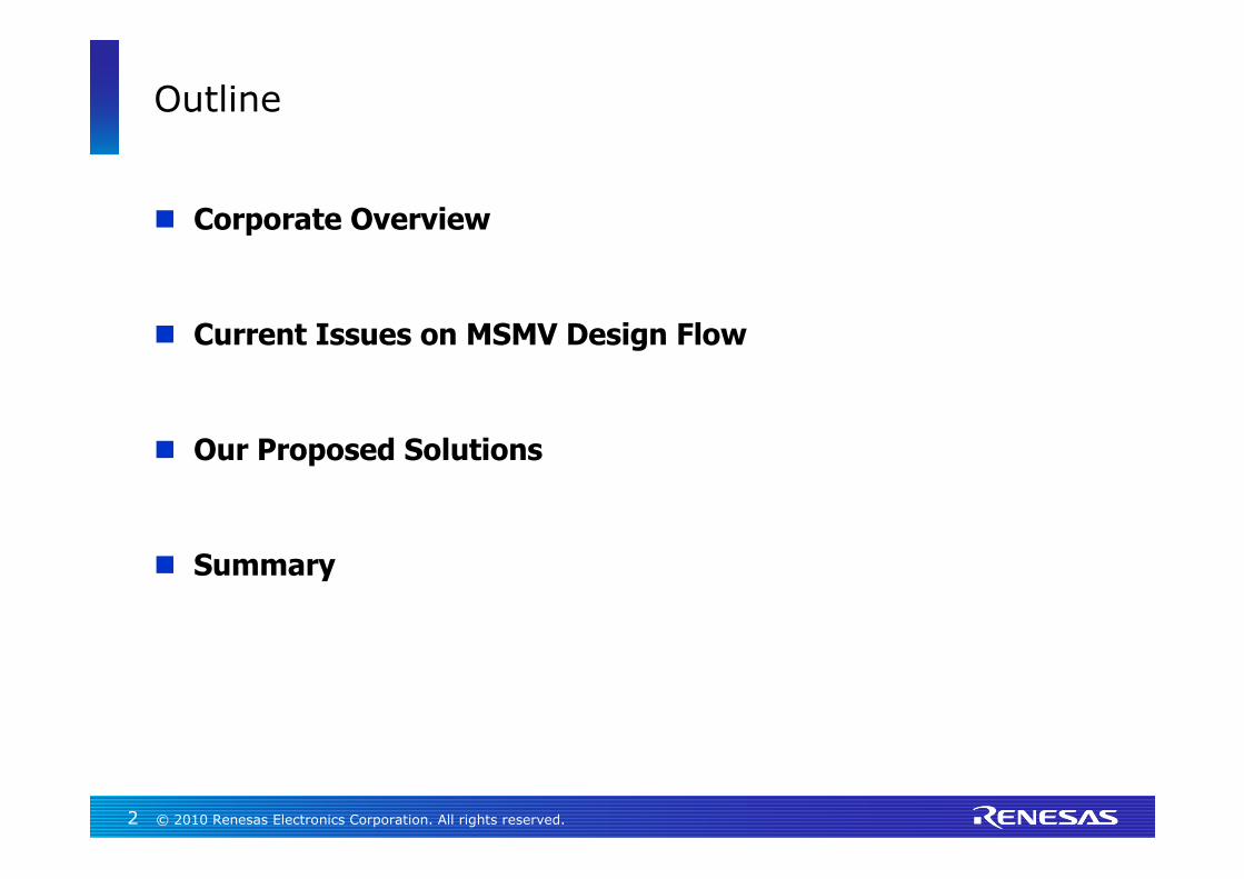
Corporate OverviewCorporate Overview
4 © 2010 Renesas Electronics Corporation. All rights reserved.
NEC
Hitachi
MitsubishiElectric
Others
NEC:NEC Corporation, Hitachi: Hitachi, Ltd., Mitsubishi Electric: Mitsubishi Electric Corporation
34%
31%
25%
10%
Merged on April 1st 2010
Corporate Overview
Shareholder Structure
5 © 2010 Renesas Electronics Corporation. All rights reserved.
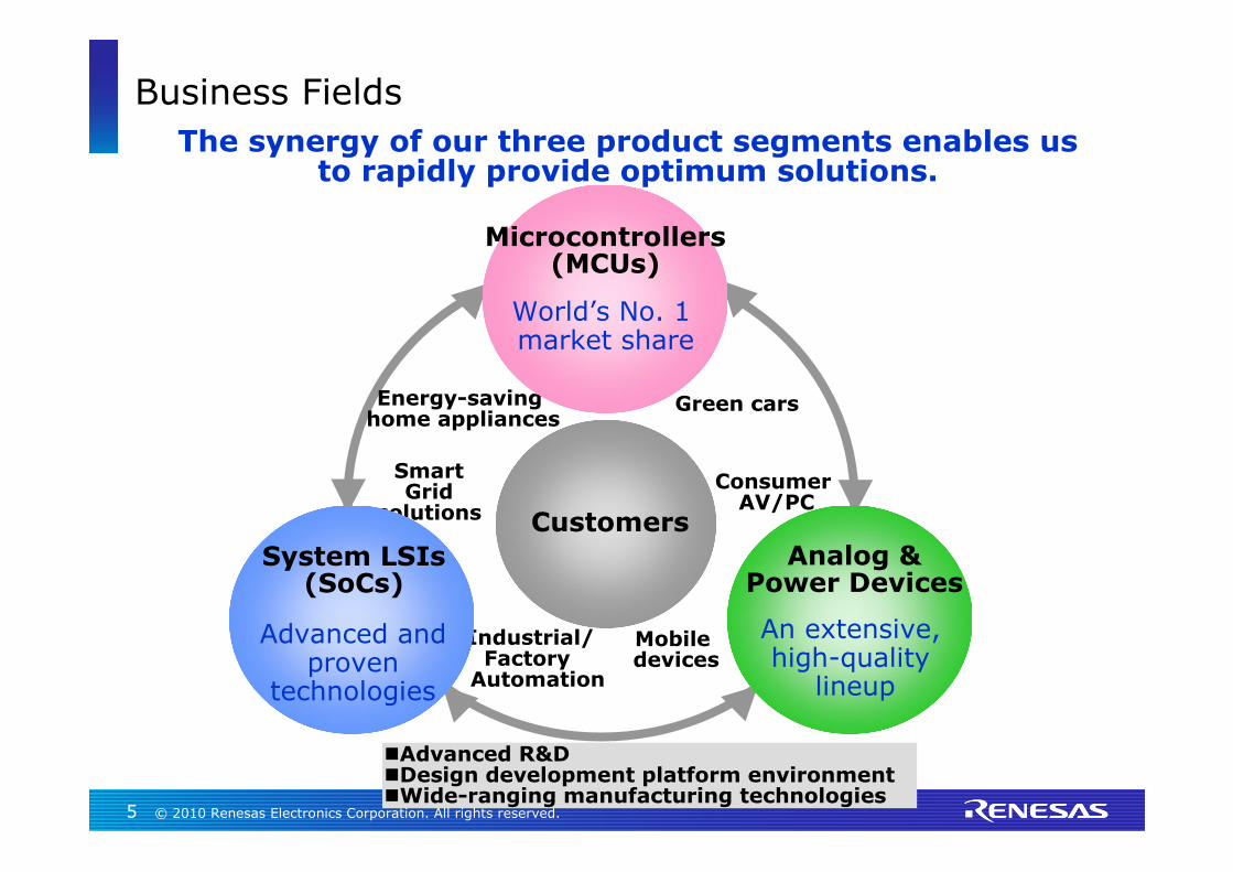
Business Fields
Smart Grid
solutions
Green cars
Industrial/Factory
Automation
Mobile devices
Consumer AV/PC
Customers
Energy-savinghome appliances
Microcontrollers(MCUs)
World’s No. 1 market share
System LSIs(SoCs)
Advanced and proven
technologies
Analog &Power Devices
An extensive, high-quality
lineup
Advanced R&D Design development platform environment Wide-ranging manufacturing technologies
The synergy of our three product segments enables us to rapidly provide optimum solutions.
6 © 2010 Renesas Electronics Corporation. All rights reserved.
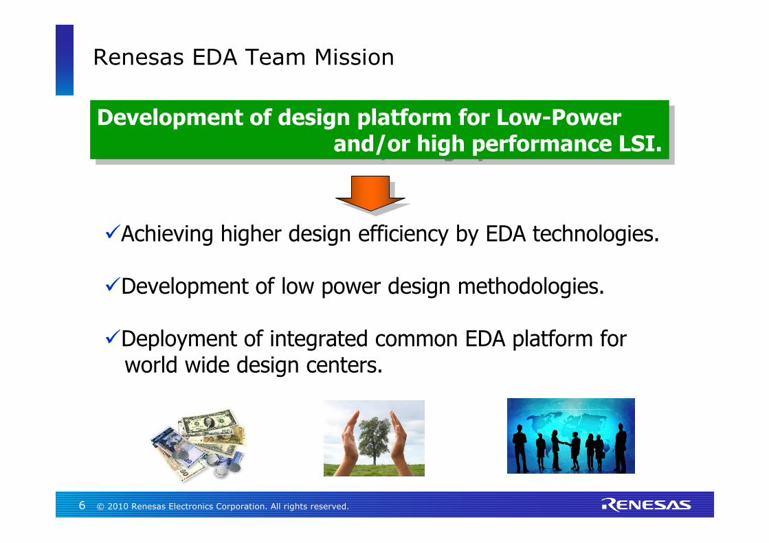
Renesas EDA Team Mission
Development of design platform for Low-Power and/or high performance LSI.
Development of design platform for Low-Power and/or high performance LSI.
Achieving higher design efficiency by EDA technologies.
Development of low power design methodologies.
Deployment of integrated common EDA platform for world wide design centers.
7 © 2010 Renesas Electronics Corporation. All rights reserved.
Current IssueCurrent Issues on MSMV Design Flows on MSMV Design Flow
8 © 2010 Renesas Electronics Corporation. All rights reserved.
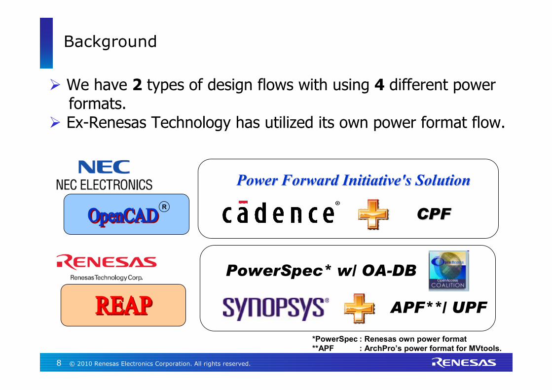
RCPFCPF
We have 2 types of design flows with using 4 different powerformats.
Ex-Renesas Technology has utilized its own power format flow.
APF**/ UPF
*PowerSpec : Renesas own power format**APF : ArchPro’s power format for MVtools.
Background
PowerSpec* w/ OA-DB
Power Forward Initiative's Solution Power Forward Initiative's Solution
9 © 2010 Renesas Electronics Corporation. All rights reserved.
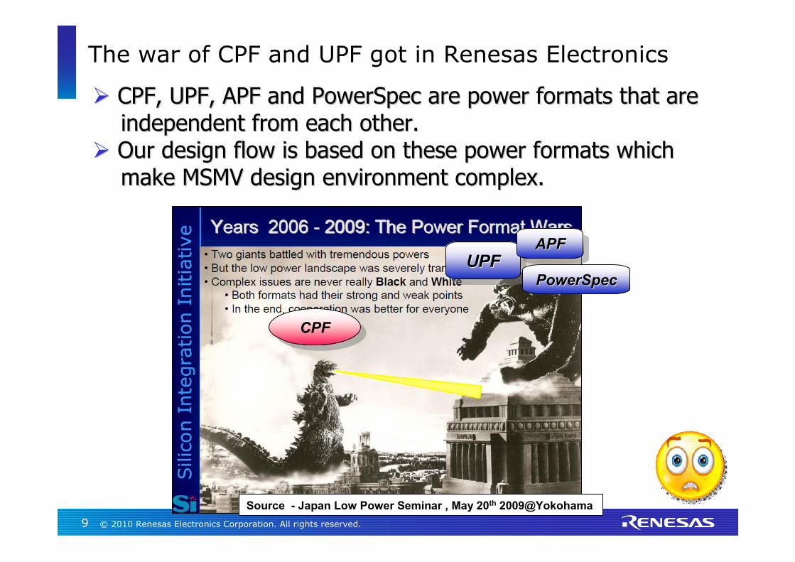
The war of CPF and UPF got in Renesas Electronics
CPF, UPF, CPF, UPF, APF APF and PowerSpec are power formats that areand PowerSpec are power formats that areindependent from each other.independent from each other.
Our design flow is based on Our design flow is based on these power formats which these power formats which make MSMV design environment complex.make MSMV design environment complex.
Source - Japan Low Power Seminar , May 20th 2009@Yokohama
CPFCPF
UPFUPFUPFPowerSpecPowerSpec
APFAAPFPF
10 © 2010 Renesas Electronics Corporation. All rights reserved.
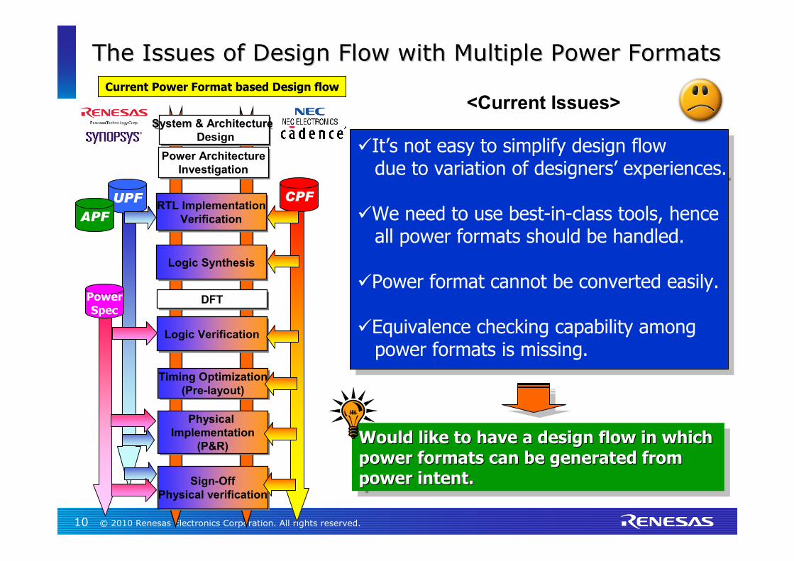
RTL ImplementationVerification
RTL ImplementationVerification
DFTDFT
Logic SynthesisLogic Synthesis
Physical Implementation
(P&R)
Physical Implementation
(P&R)
Sign-OffPhysical verification
Sign-OffPhysical verification
System & Architecture Design
System & Architecture Design
Timing Optimization(Pre-layout)
Timing Optimization(Pre-layout)
Power ArchitectureInvestigation
Power ArchitectureInvestigation
CPFUPF
PowerSpec
Logic VerificationLogic Verification
The Issues of Design Flow with Multiple Power FormatsThe Issues of Design Flow with Multiple Power FormatsCurrent Power Format based Design flow
<Current Issues>
Would like to have a design flow in which power formats can be generated from power intent.
Would like to have a design flow in which Would like to have a design flow in which power formats can be generated from power formats can be generated from power intent.power intent.
APF
It’s not easy to simplify design flowdue to variation of designers’ experiences.
We need to use best-in-class tools, hence all power formats should be handled.
Power format cannot be converted easily.
Equivalence checking capability amongpower formats is missing.
It’s not easy to simplify design flowdue to variation of designers’ experiences.
We need to use best-in-class tools, hence all power formats should be handled.
Power format cannot be converted easily.
Equivalence checking capability amongpower formats is missing.
11 © 2010 Renesas Electronics Corporation. All rights reserved.
Our ProposedOur Proposed SolutionSolution
12 © 2010 Renesas Electronics Corporation. All rights reserved.
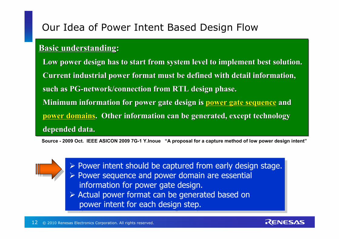
Our Idea of Power Intent Based Design Flow
Basic understanding:Low power design has to start from system level to implement best solution.
Current industrial power format must be defined with detail information,
such as PG-network/connection from RTL design phase.
Minimum information for power gate design is power gate sequence and
power domains. Other information can be generated, except technology
depended data.
Basic understandingBasic understanding::Low power design has to start from system level to implement bLow power design has to start from system level to implement best solution. est solution.
Current industrial power format must be defined with detail inCurrent industrial power format must be defined with detail information,formation,
such as PGsuch as PG--network/connection from RTL design phase. network/connection from RTL design phase.
Minimum information for power gate design is Minimum information for power gate design is power gate sequencepower gate sequence andand
power domainspower domains. Other information can be generated, except technology. Other information can be generated, except technology
depended data.depended data.Source - 2009 Oct. IEEE ASICON 2009 7G-1 Y.Inoue “A proposal for a capture method of low power design intent”
Power intent should be captured from early design stage. Power sequence and power domain are essential
information for power gate design. Actual power format can be generated based on
power intent for each design step.
Power intent should be captured from early design stage. Power sequence and power domain are essential
information for power gate design. Actual power format can be generated based on
power intent for each design step.
13 © 2010 Renesas Electronics Corporation. All rights reserved.
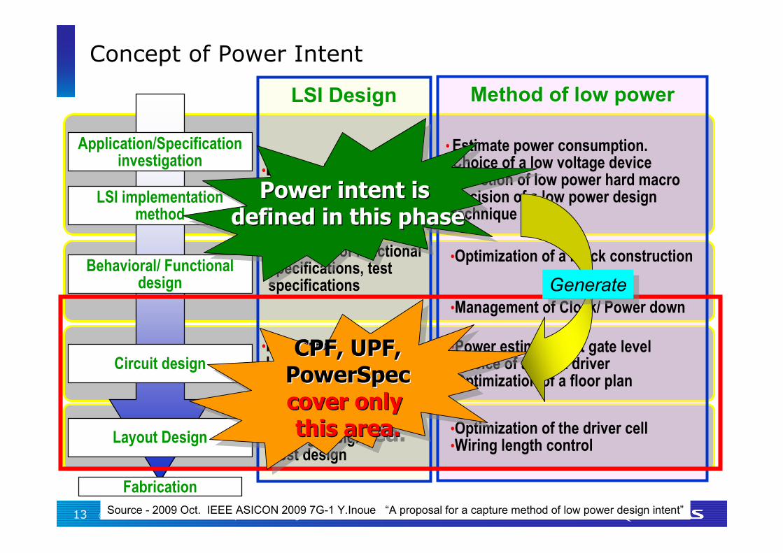
LSI Design Method of low power
•Expected specification•Partition to LSI
•Document of functional specifications, test specifications
•Functional description•Logic synthesis•Function verification
•Layout design•Timing design•Test design
•Estimate power consumption.•Choice of a low voltage device•Selection of low power hard macro•Decision of a low power design technique
•Optimization of a block construction
•Management of Clock/ Power down
•Power estimation at gate level•Choice of a clock driver•Optimization of a floor plan
•Optimization of the driver cell•Wiring length control
Application/Specificationinvestigation
LSI implementationmethod
Behavioral/ Functionaldesign
Circuit design
Layout Design
Fabrication
Concept of Power Intent
Source - 2009 Oct. IEEE ASICON 2009 7G-1 Y.Inoue “A proposal for a capture method of low power design intent”
CPF, UPF,PowerSpeccover only this area.
CPF, UPF,CPF, UPF,PowerSpecPowerSpeccover only cover only this area.this area.
Power intent is defined in this phase
Power intent is Power intent is defined in this phasedefined in this phase
GenerateGenerate
14 © 2010 Renesas Electronics Corporation. All rights reserved.
Actual power format can be generated from power intent. Actual power format can be generated from power intent.
CPU1CPU1
memorymemory IPsIPs
Peripheralmodule
PeripheralmoduleCPU2CPU2
Mode1
Mode2
E1
E2E3
E4
State transition of power mode
Mode3
Mode4
E5
E6
Domain 1:VDD: 1.2VPower gate: YES
Domain 2:VDD: 1.2VPower gate: NO
Domain 3:VDD: 3.3VPower gate: YES
<Power Intent>
CPU1CPU1
memorymemory IPsIPs
Peripheralmodule
PeripheralmoduleCPU2CPU2
LS
Domain 1:VDD: 1.2VPower gate: YESControl sig : en1
:
Domain 2:VDD: 1.2VPower gate: NO
Domain 3:VDD: 3.3VPower gate: YESControl sig : en3
:
ISO
ISO
LS
VSW
LS : Level ShiftersISO: Isolation cellsVSW: Power gate switch
ISO
<Low Power LSI Spec>PowerFormat
How can we define Power Intent ?
Generate
Source - 2009 Oct. IEEE ASICON 2009 7G-1 Y.Inoue “A proposal for a capture method of low power design intent”
15 © 2010 Renesas Electronics Corporation. All rights reserved.
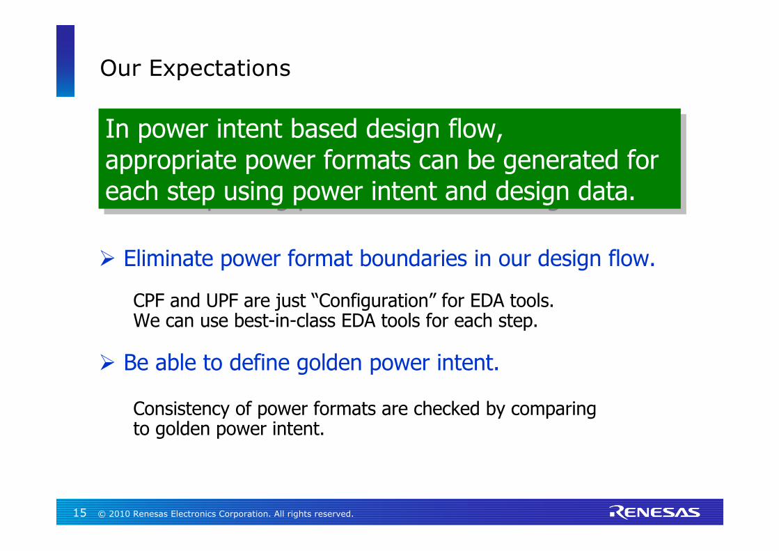
Our Expectations
Eliminate power format boundaries in our design flow.
CPF and UPF are just “Configuration” for EDA tools.We can use best-in-class EDA tools for each step.
Be able to define golden power intent.
Consistency of power formats are checked by comparing to golden power intent.
In power intent based design flow, appropriate power formats can be generated for each step using power intent and design data.
In power intent based design flow, appropriate power formats can be generated for each step using power intent and design data.
16 © 2010 Renesas Electronics Corporation. All rights reserved.
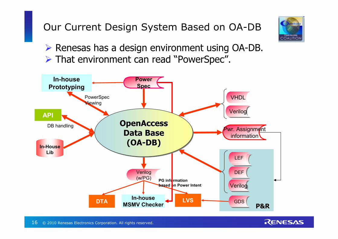
P&RP&R
VerilogVerilog
Verilog(w/PG)
GDSGDSLVSDTA
In-housePrototyping
API
VHDL
DEFDEF
In-HouseLib
PowerSpec
Pwr. Assignmentinformation
Renesas has a design environment using OA-DB. That environment can read “PowerSpec”.
Our Current Design System Based on OA-DB
LEFLEFLEF
In-houseMSMV Checker
PowerSpecViewing
DB handling
PG informationbased on Power Intent
VerilogVerilog
OpenAccessData Base(OA-DB)
OpenAccessOpenAccessData BaseData Base(OA(OA--DB)DB)
17 © 2010 Renesas Electronics Corporation. All rights reserved.
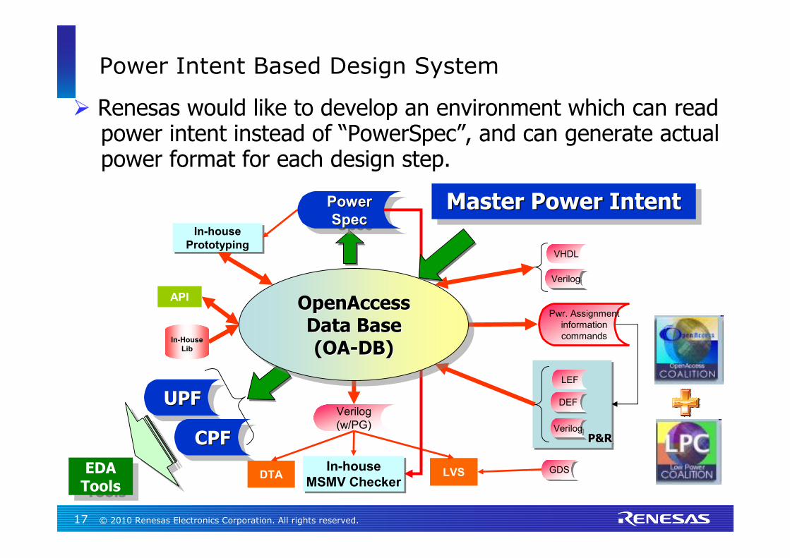
Renesas would like to develop an environment which can read power intent instead of “PowerSpec”, and can generate actual power format for each design step.
Power Intent Based Design System
UPFUPUPFF
P&RP&RP&RVerilogVerilog
Verilog(w/PG)
GDSGDSLVSDTA
In-housePrototypingIn-house
Prototyping
API
VHDL
DEFDEF
In-HouseLib
PowerSpec
PowerPowerSpecSpec
LEF
In-houseMSMV Checker
In-houseMSMV Checker
VerilogVerilog
OpenAccessData Base(OA-DB)
OpenAccessOpenAccessData BaseData Base(OA(OA--DB)DB)
Master Power IntentMaster Master Power IntentPower Intent
Pwr. Assignmentinformationcommands
CPFCPCPFF
EDAToolsEDA
Tools
18 © 2010 Renesas Electronics Corporation. All rights reserved.
Summary
19 © 2010 Renesas Electronics Corporation. All rights reserved.
Concept of power intent based design flow is shown.
Actual power formats can be generated from power intent for each design step.
We are expecting that OA-DB will be one of the solutions to generate actual power formats.
Summary

20 © 2010 Renesas Electronics Corporation. All rights reserved.
Thank youThank youfor your attention.for your attention.
© 2010 Renesas Electronics Corporation. All rights reserved.
Renesas Electronics Corporation


![INVENTIVE - Si2projects.si2.org/events_dir/2007/date/cadence.pdf · INVENTIVE Common Power Format: ... ATPG Constraint Validation Equivalence checking ... [ -sdc_files sdc_file_list]](https://img.pdfslide.us/doc/110x75/5ac901cf7f8b9aa3298c99f7/inventive-common-power-format-atpg-constraint-validation-equivalence-checking.jpg)