Embed Size (px)
Citation preview
this stage is induced by the linear variation of the admittance along thez-axis. The current shape at a given position z can be explained usingthe plots of Figures 6(a), 6(b), and 7. As an example, considering theposition z0 � 2.4 cm, the top current component I�top0(z, t, � � 0)appears as the superposition of current elements positioned betweenz � 0 and z � z0 [see Fig. 6(a)]; as z increases up to z0, the amplitudeof the incident pulse increases, and a left time shift is observed. Thesum of the contributions of the several current elements gives adistorted version of the first derivative of the Gaussian function. Thebottom component I�bottom0(z, t, � � 0) is the superposition of currentelements positioned between z � z0 and z � L [see Fig. 6(b)]; theamplitude of the elements increases with z and a right time shift isobserved. Thus, the sum shows a stage as the positive and negativeamplitudes increases linearly, and at both limits the shape of the sumdepends on the pulses duration relative to the propagation time alongthe antenna. The shape of the sum of the top and bottom componentsis presented in Figure 7.
4.3. Case of a V-dipoleIn the case of a straight dipole (�L, L), which represents aparticular V-dipole characterized by an aperture angle 2� � 180°,we have verified that the several current components included inrelation (17) corresponds to the relation given by Samaddar andMokole, which is only valid at the position z � 0 [5].
Then, we have studied a V-dipole with arm length L � 10 cm,and an aperture angle 2� � 120°. At first, we have not included inthe results presented the convolution product mentioned in relation(9) to analyze in detail the initial current waveforms. Thus, Figures8(a) and 8(b) show the influence of the angle of incidence (� � 0°,10°, and 30°) on the current distribution along the antenna. FromFigure 8(a), we can observe that the current amplitude is weak atboth ends z � L and z � �L because of the presence of a highimpedance, and it increases gradually towards z � 0. At theposition z � 0, Figure 8(b) shows that an increasing angle ofincidence produces an increasing time delay, and an increasingduration of the negative part expressing the fact that both arms arenot illuminated at the same time.
Including now the convolution product of the current distribu-tion plotted in Figure 8(a) with the exponential function accordingto relation (9), Figure 9 highlights that this additional operationcontributes to smooth the waveforms.
5. CONCLUSION
In this paper, the analytical modelling associated with the excita-tion of a Wu and King loaded dipole (0, L) by a transientelectric-plane wavefront has been revisited. As the electric fieldinteracts with discrete elements positioned along the dipole that actas small sources, the modelling formulated in the time domain usestraveling current waves to represent the current distribution alongthe dipole. The modelled current appears as a sum of two compo-nents associated with: (i) a uniform infinitely conductive dipoleand (ii) a dipole whose admittance decreases linearly versus itsdirection z. Such a decomposition allows to highlight the contri-bution of each component to the total current induced in the dipole.Moreover, we have remarked that the distributed admittance pro-duces a current tail absent when the dipole is uniform. This tail isdue to the noncompensating effect of the discrete delayed sourceelements as their amplitudes decrease towards the end z � L. Adetailed analysis of the different components has been proposed.The modelling has been validated in the case where z � 0 usingthe analytical developments made by Samaddar and Mokole for astraight dipole (�L, L) [5]. The study of a V-dipole has beenconsidered as a first step towards further dipole combinations torepresent more complex geometries in the 2D or 3D space domain.
REFERENCES
1. T.P. Montoya and G.S. Smith, Land mine detection using a ground-penetrating radar based on resistively loaded Vee dipoles, IEEE TransAntennas Propagat 47 (1999), 1795–1806.
2. M. Kanda, Time-domain sensors for radiated impulse measurements,IEEE Trans Antennas Propagat 31 (1983), 438–444.
3. L. Yang and G.B. Giannakis, Ultra-wideband communications: An ideawhose time has come, IEEE Signal Processing Mag (2004), 26–53.
4. T.T. Wu and R.W.P. King, The cylindrical antenna with nonreflectingresistive loading, IEEE Trans Antennas Propagat 13 (1965), 369–373.
5. S.N. Samaddar and E.L. Mokole, Transient behaviour of radiated andreceived fields associated with a resistively loaded dipole, Ultra-wide-band short electromagnetics 4, Herman et al. (Eds.), Kluwer Academic–Plenum Publishers, New York, 1999, pp. 165–179.
6. D.L. Sengupta and C.T. Tai, Transient electromagnetic fields, L.B.Felsen (Ed.), 1976.
7. F. Sagnard, B. Uguen, and G. El Zein, Reception of an oblique elec-tromagnetic plane wave by a linear-wire antenna: A time-domain anal-ysis, Microwave Opt Technol Lett 38 (2003), 281–291.
8. F. Sagnard and C. Vignat, Extension of the analytical modeling ofresistive loaded thin-wire antennas to Gaussian derivatives excitations,Microwave Opt Technol Lett 47 (2005), 548–553.
© 2006 Wiley Periodicals, Inc.
A SMALL WIDEBAND PLANARMONOPOLE ANTENNA FOR MOBILEWIRELESS DEVICES
Jihak Jung, Yeonsik Yu, and Jaehoon ChoiDepartment of Electrical and Computer EngineeringHanyang University17 Haengdang-dong, Seongdong-guSeoul, 133-791, Korea
Received 14 October 2005
ABSTRACT: A small wideband planar monopole antenna for mobilewireless devices is designed and implemented. The proposed antennasatisfies the �10-dB return-loss requirement from 1.62 to 10.9 GHz.
Figure 9 Time and spatial representation of the current distributioninduced in a V-dipole with aperture angle 2� � 120° at incidence � � 0°(with a convolution product). [Color figure can be viewed in the onlineissue, which is available at www.interscience.wiley.com]
736 MICROWAVE AND OPTICAL TECHNOLOGY LETTERS / Vol. 48, No. 4, April 2006 DOI 10.1002/mop
The antenna can easily cover the DCS1800/1900, IMT-2000, WiBro,WLAN, DMB, and UWB bands at the same time. The experimental andnumerical results of the designed wideband antenna are presented andanalyzed. © 2006 Wiley Periodicals, Inc. Microwave Opt Technol Lett48: 736–740, 2006; Published online in Wiley InterScience (www.interscience.wiley.com). DOI 10.1002/mop.21460
Key words: mobile wireless device; planar monopole antenna; systemground plane; ultra-wideband antenna
1. INTRODUCTION
Nowdays, much attention has been paid to new technologies inwireless communication systems. These new communication tech-nologies are very promising for realizing the software-defined andreconfigurable wireless systems. Antennas for such systems shouldbe capable of operating over ultra-wideband or multiband schemein order to be flexible enough to accommodate any possible futuremobile communication frequency bands.
To provide such flexibility, the use of a single wideband an-tenna, which covers a wide range of frequencies, is desirable forthe emerging software defined and/or reconfigurable wireless sys-tems. This antenna should be as small as possible to fit the severespace constraints imposed on the mobile wireless devices. Theplanar monopole antenna is a good candidate for mobile devices,due to its wide impedance bandwidth, compact and simple struc-ture, low cost, and ease of construction. Recently, it has beendemonstrated that wideband monopole antennas [1–4] is promis-ing to be used for mobile wireless devices such as notebookcomputers, mobile phones, and PDA phones.
In this paper, we propose a small wideband planar monopoleantenna covering all the desired frequency bands, such asDCS1800 (1.71–1.88 GHz) or 1900 (1.85–1.99 GHz), IMT-2000(1.885–2.2 GHz), WiBro (2.3–2.39 GHz), WLAN (2.412–2.483GHz), DMB (2.63–2.655 GHz), and UWB (3.1–10.6 GHz). Theparametric analysis for antenna configuration is performed byexperimental and numerical ways.
2. ANTENNA DESIGN
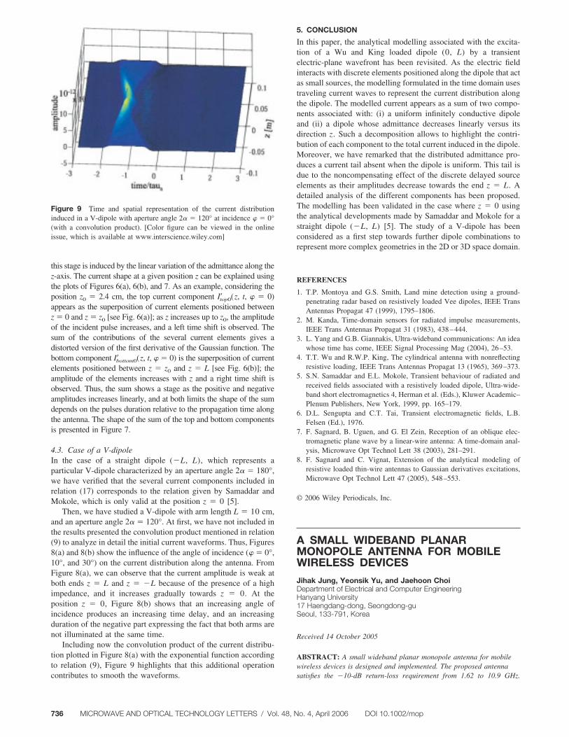
Figure 1(a) shows the basic configuration of the proposed wide-band antenna, which consists of a radiating patch with a slot andstub at the left side. The antenna having dimension of 18 � 28mm2 (Wsub � Lsub) is constructed on FR4 substrate with thicknessh of 1.6 mm and relative dielectric constant �r of 4.4. Figure 1(b)shows the antenna configuration including the system groundwhich simulates the case of a practical mobile phone or PDAphone.
The proposed antenna is mounted on a small ground plane(10 � 18 mm2) protruding from the system ground (40 � 65mm2). A small 10 � 18 � 28 mm3 space at one of the uppercorners of the system ground plane is required to accommodate theantenna. The size of the system ground plane is determined tosimulate the actual mobile phone or PDA phone. These dimensions(Wsys grd, Lsys grd) are also recognized as important parameters fordetermining the sensitivity of impedance matching at lower fre-quencies [1, 5, 6]. Effects of the variation in antenna dimensions ofthe system ground plane on the impedance matching will beexplored in section 3. As shown in Figure 1(a), a widebandcharacteristic of the proposed antenna is easily achieved by insert-ing the slot and attaching a stub to the radiating patch. The slotwith proper dimensions (W1 � L1) improves the impedancematching performance at the middle frequencies within the band-width of interest.
This phenomenon occurs because the slot provides the capac-itive coupling to the antenna’s input impedance [7, 8]. To achievesuperior impedance matching at lower and higher frequencies, astub (W2, L2) is appended to the left side of the radiating patch.The optimal dimension of the designed antenna determined frommany experimental and simulated results are as follows: Wsys grd �40 mm, Lsys grd � 65 mm, Wsub � 18 mm, Lsub � 28 mm, W �13 mm, L � 16 mm, W1 � 9 mm, L1 � 3 mm, W2 � 1 mm,L2 � 10 mm, d � 10 mm, Wf � 2 mm, and Lgrd � 6 mm. InFigure 1(c), the fabricated antenna is compared to the practicalmobile phone. The proposed antenna is designed to operate overthe frequency band ranging from 1.62 to 10.9 GHz.
3. EXPERIMENTAL RESULTS
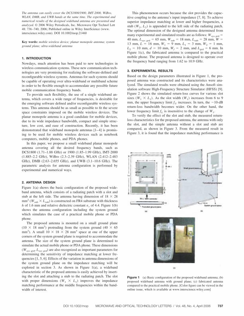
Based on the design parameters illustrated in Figure 1, the pro-posed antenna was constructed and its characteristics were ana-lyzed. The simulated results were obtained using the Ansoft sim-ulation software High-Frequency Structure Simulator (HFSS) [9].Figure 2 shows the simulated return-loss curves for various slotsizes (W1 � L1). As the slot width (W1) increases from 6 to 9mm, the upper frequency limit fU increases. In turn, the �10-dBreturn-loss bandwidth becomes wider. On the other hand, thelower frequency limit fL is insensitive to the change of W1.
To verify the effect of the slot and stub, the measured return-loss characteristics for the proposed antenna, the antenna with onlythe slot, and the simple antenna without a slot and stub arecompared, as shown in Figure 3. From the measured result inFigure 3, it is found that the impedance matching performance is
Figure 1 (a) Basic configuration of the proposed wideband antenna; (b)proposed wideband antenna with ground plane; (c) fabricated antennacompared to the practical mobile phone. [Color figure can be viewed in theonline issue, which is available at www.interscience.wiley.com]
DOI 10.1002/mop MICROWAVE AND OPTICAL TECHNOLOGY LETTERS / Vol. 48, No. 4, April 2006 737
improved effectively at frequencies between 2.7 and 9 GHz by theaddition of the slot. By adjusting the length of a stub, it is alsoobserved that the impedance bandwidth is not only enhanced athigher frequencies above 9 GHz, but also improved at lowerfrequencies.
Figure 4 shows the simulated and measured return-loss curvesof the proposed antenna. The measured impedance bandwidth iswider than the simulated one in Figure 4. The fabricated antennasatisfies the 10 dB return loss requirement from 1.62 to 10.9 GHz.
In order to investigate the effect of system ground-plane size onthe proposed antenna, the return-loss characteristics for variousground-plane sizes (Wsys grd, Lsys grd) were analyzed. As shown inFigure 5, the measured results indicate that the change in thesystem ground-plane width (Wsys grd) affects the bandwidth per-formance, especially at lower frequencies. Several experimentalresults in [1] revealed that the excited surface current distributionsin the system ground plane is more sensitive to variation in Wsys grd
than one in Lsys grd.
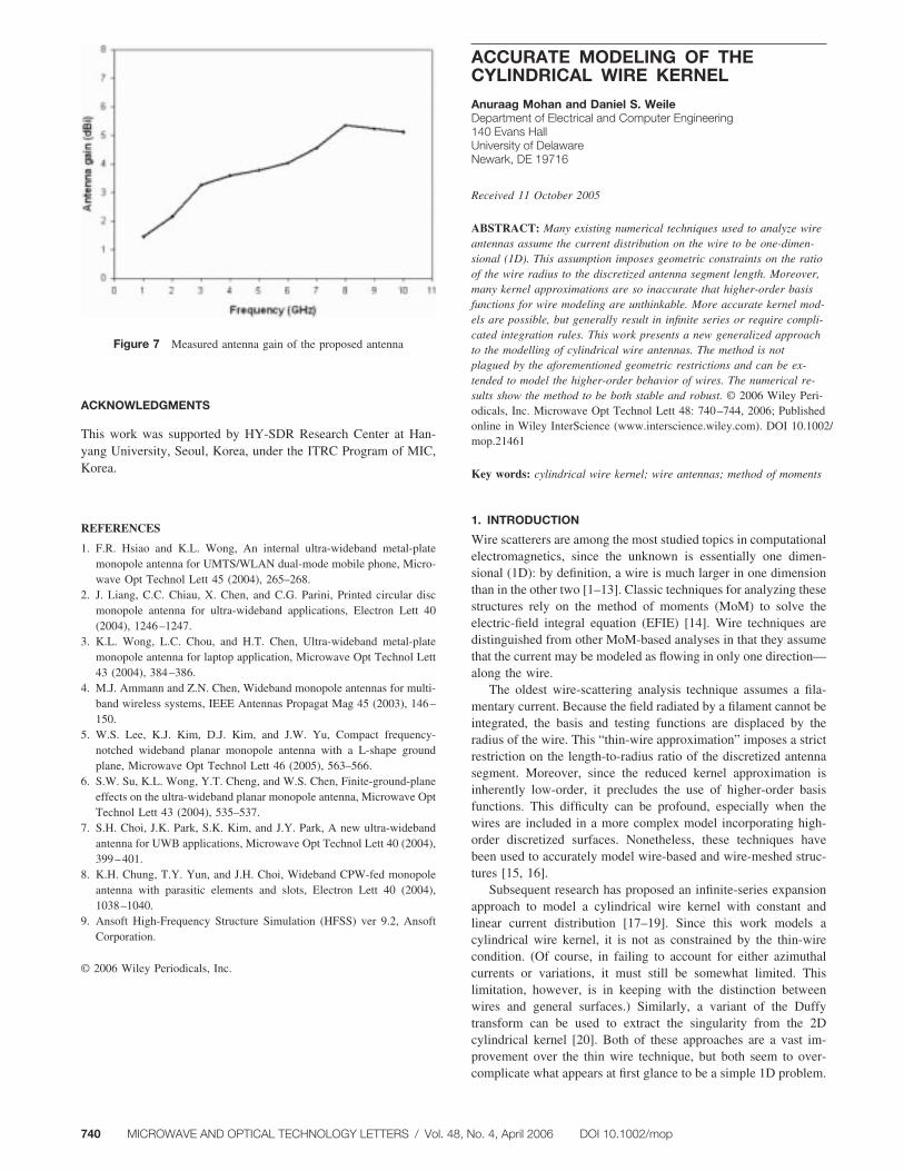
Figure 6 shows the measured radiation patterns for the pro-posed antenna at 1.9, 5, and 8 GHz. Monopolelike radiationpatterns in the y–z planes are observed. The radiation patterns inthe x–z planes are approximately omnidirectional, especially forthe higher operating frequencies. Figure 7 shows the measuredantenna gain plotted against frequency. The antenna gain is vary-ing from about 1.4 to 5.32 dBi across the entire bandwidth.
4. CONCLUSION
A small wideband monopole antenna suitable for various mobilecommunication applications has been presented. The proposedantenna has a simple configuration and is easy to fabricate. Thisantenna is capable of covering the existing DCS1800, DCS1900,IMT-2000, WiBro, WLAN, DMB, and UWB bands simulta-neously. The effects of the system ground-plane size on the im-pedance matching of the proposed antenna have also been inves-tigated.
Figure 2 Simulated return loss for the proposed monopole antenna withvarious slot widths W1 (L1 is fixed at 3 mm)
Figure 3 Comparison of measured return-loss characteristics for theproposed antenna, the antenna with slot only, and the simple antennawithout slot and stub
Figure 4 Measured and simulated return losses for the proposed antenna
Figure 5 Measured return losses for the proposed antenna with varioussystem ground plane widths (Wsys grd)
738 MICROWAVE AND OPTICAL TECHNOLOGY LETTERS / Vol. 48, No. 4, April 2006 DOI 10.1002/mop
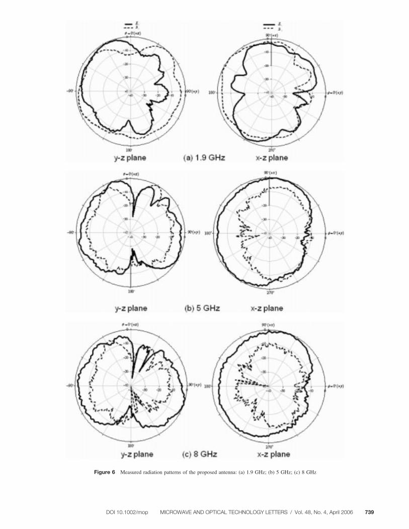
Figure 6 Measured radiation patterns of the proposed antenna: (a) 1.9 GHz; (b) 5 GHz; (c) 8 GHz
DOI 10.1002/mop MICROWAVE AND OPTICAL TECHNOLOGY LETTERS / Vol. 48, No. 4, April 2006 739
ACKNOWLEDGMENTS
This work was supported by HY-SDR Research Center at Han-yang University, Seoul, Korea, under the ITRC Program of MIC,Korea.
REFERENCES
1. F.R. Hsiao and K.L. Wong, An internal ultra-wideband metal-platemonopole antenna for UMTS/WLAN dual-mode mobile phone, Micro-wave Opt Technol Lett 45 (2004), 265–268.
2. J. Liang, C.C. Chiau, X. Chen, and C.G. Parini, Printed circular discmonopole antenna for ultra-wideband applications, Electron Lett 40(2004), 1246–1247.
3. K.L. Wong, L.C. Chou, and H.T. Chen, Ultra-wideband metal-platemonopole antenna for laptop application, Microwave Opt Technol Lett43 (2004), 384–386.
4. M.J. Ammann and Z.N. Chen, Wideband monopole antennas for multi-band wireless systems, IEEE Antennas Propagat Mag 45 (2003), 146–150.
5. W.S. Lee, K.J. Kim, D.J. Kim, and J.W. Yu, Compact frequency-notched wideband planar monopole antenna with a L-shape groundplane, Microwave Opt Technol Lett 46 (2005), 563–566.
6. S.W. Su, K.L. Wong, Y.T. Cheng, and W.S. Chen, Finite-ground-planeeffects on the ultra-wideband planar monopole antenna, Microwave OptTechnol Lett 43 (2004), 535–537.
7. S.H. Choi, J.K. Park, S.K. Kim, and J.Y. Park, A new ultra-widebandantenna for UWB applications, Microwave Opt Technol Lett 40 (2004),399–401.
8. K.H. Chung, T.Y. Yun, and J.H. Choi, Wideband CPW-fed monopoleantenna with parasitic elements and slots, Electron Lett 40 (2004),1038–1040.
9. Ansoft High-Frequency Structure Simulation (HFSS) ver 9.2, AnsoftCorporation.
© 2006 Wiley Periodicals, Inc.
ACCURATE MODELING OF THECYLINDRICAL WIRE KERNEL
Anuraag Mohan and Daniel S. WeileDepartment of Electrical and Computer Engineering140 Evans HallUniversity of DelawareNewark, DE 19716
Received 11 October 2005
ABSTRACT: Many existing numerical techniques used to analyze wireantennas assume the current distribution on the wire to be one-dimen-sional (1D). This assumption imposes geometric constraints on the ratioof the wire radius to the discretized antenna segment length. Moreover,many kernel approximations are so inaccurate that higher-order basisfunctions for wire modeling are unthinkable. More accurate kernel mod-els are possible, but generally result in infinite series or require compli-cated integration rules. This work presents a new generalized approachto the modelling of cylindrical wire antennas. The method is notplagued by the aforementioned geometric restrictions and can be ex-tended to model the higher-order behavior of wires. The numerical re-sults show the method to be both stable and robust. © 2006 Wiley Peri-odicals, Inc. Microwave Opt Technol Lett 48: 740–744, 2006; Publishedonline in Wiley InterScience (www.interscience.wiley.com). DOI 10.1002/mop.21461
Key words: cylindrical wire kernel; wire antennas; method of moments
1. INTRODUCTION
Wire scatterers are among the most studied topics in computationalelectromagnetics, since the unknown is essentially one dimen-sional (1D): by definition, a wire is much larger in one dimensionthan in the other two [1–13]. Classic techniques for analyzing thesestructures rely on the method of moments (MoM) to solve theelectric-field integral equation (EFIE) [14]. Wire techniques aredistinguished from other MoM-based analyses in that they assumethat the current may be modeled as flowing in only one direction—along the wire.
The oldest wire-scattering analysis technique assumes a fila-mentary current. Because the field radiated by a filament cannot beintegrated, the basis and testing functions are displaced by theradius of the wire. This “thin-wire approximation” imposes a strictrestriction on the length-to-radius ratio of the discretized antennasegment. Moreover, since the reduced kernel approximation isinherently low-order, it precludes the use of higher-order basisfunctions. This difficulty can be profound, especially when thewires are included in a more complex model incorporating high-order discretized surfaces. Nonetheless, these techniques havebeen used to accurately model wire-based and wire-meshed struc-tures [15, 16].
Subsequent research has proposed an infinite-series expansionapproach to model a cylindrical wire kernel with constant andlinear current distribution [17–19]. Since this work models acylindrical wire kernel, it is not as constrained by the thin-wirecondition. (Of course, in failing to account for either azimuthalcurrents or variations, it must still be somewhat limited. Thislimitation, however, is in keeping with the distinction betweenwires and general surfaces.) Similarly, a variant of the Duffytransform can be used to extract the singularity from the 2Dcylindrical kernel [20]. Both of these approaches are a vast im-provement over the thin wire technique, but both seem to over-complicate what appears at first glance to be a simple 1D problem.
Figure 7 Measured antenna gain of the proposed antenna
740 MICROWAVE AND OPTICAL TECHNOLOGY LETTERS / Vol. 48, No. 4, April 2006 DOI 10.1002/mop


![DESIGN AND ANALYSIS OF WIDEBAND PLANAR MONOPOLE ANTENNAS … · 2020. 1. 16. · planar monopole antennas have attracted many studies. Techniques such as adding shorting posts [10{12],](https://img.pdfslide.us/doc/110x75/60d5231b18413f5a56506387/design-and-analysis-of-wideband-planar-monopole-antennas-2020-1-16-planar-monopole.jpg)