Embed Size (px)
Citation preview
22 High Frequency Electronics
Power Amp Design
A simulation-based methodology for
broadband power amplifier design.
A Simulation-Based Design Flow for Broadband GaN Power Amplifier Design
By Ivan Boshnakov, Malcolm Edwards, Larry Dunleavy, Isabella Delgado
The purpose of this note is to demonstrate a simulation-based method-ology for broadband power amplifier design using load-line, load-pull, and real-frequency synthesis techniques. The design shown in this application note is a Class F amplifier and was created using the Qorvo 30W GaN HEMT T2G6003028-FL transistor. Goals for this design were: a minimum output power of 25W, bandwidth of 1.8 - 2.2GHz, and maximum power
added efficiency (PAE). The design procedure was performed using the Modelithics GaN HEMT non-linear model for the Qorvo transistor mentioned above; Modelithics Microwave Global Models for the passive components in the matching network design; and the Amplifier Design Wizard (ADW) from AMPSA (all tools available within suitably configured NI AWR’s Microwave Office).
Design OverviewFor this design methodology it is crucial to have access to the intrinsic device channel volt-
age and current. Such capabilities are available in the advanced non-linear Modelithics GaN models. The design begins with measurements of the voltage and current at the drain-source intrinsic current generator within Microwave Office. The near optimum load-line, impedances of the fundamental frequency, and harmonic impedances for a single frequency are located for the required mode of operation. The impedance regions are then extracted using load-pull simulations. Using ADW, the “real-frequency” synthesis of the matching networks can be quick-ly realized simultaneously for the fundamental and harmonic impedances across a wide band-width. These fully laid-out matching networks can then be exported to MWO for the remainder of the design optimization, non-linear analysis, and electromagnetic (EM) simulation.
Design ProcessTo begin the design process, a schematic to bias and stabilize the transistor must first be
drawn. Once the conditions required for stability and biasing are established, the initial load-line analysis and harmonic impedance tuning can be performed (Figure 1).
Initial Load-Line and Harmonic Impedance TuningFirst, a line is drawn on top of the IV curves to approximate the near optimum load-line for
the fundamental frequency (the maximum swing of the RF voltage and current before hard clipping occurs). Then the dynamic load-line, defined using meters located within the model to monitor the intrinsic drain voltage and current and superimposed on the IV curves by the IVDLL measurement, is tuned to be a straight line and parallel to the drawn line. The tuning at a chosen frequency is performed by tuning the magnitude and phase of the output tuner impedances. At this stage, the harmonic balance simulation is limited to just a single harmon-ic—the fundamental frequency. Additionally, the harmonic impedances of the output tuner and

24 High Frequency Electronics
Get info at www.HFeLink.com
Power Amp Design
all the impedances of the input tuner are set to 50Ω. The final results of the tuning can be seen in Figure 2.
Once the impedance of the fundamental frequency is known, the second and the third harmonic impedances presented to the intrinsic drain can be tuned according to the desired mode of operation. In the case of this application note, Class-F operation is desired, meaning that the second harmonic imped-ance is tuned to a short circuit and the third harmonic impedance is tuned to an open circuit (Figure 3).
The fundamental impedance of the input tuner is then made to be a conju-gate match to the S11 of the transistor and stability / bias network. This will provide the best match and therefore, maximum gain. The harmonic imped-ances of the input tuner are set to 50Ω.
Now that all of the impedances have been tuned, a final harmonic balance simulation (using three harmonics) is performed to confirm the design is in the desired mode of operation. Figure 4 and Figure 5 show the classic shapes of a Class-F mode design.
Ducommun has more than 45 years of experience with the design, testing and manufacturing of
standard and custom millimeter wave amplifiers.
PRODUCTSTO SOLUTIONS
RF ProductsC
ON
TAC
T U
S
For additional information, contact our sales team at
+1 (310) 513-7256 [email protected]
•High Power, Single DC power supply/internal sequential biasing
32 to 36 GHz Power AmplifierAHP-34043530-01Gain: 30 dB (Min)Gain Flatness: +/-2.0 dB (Max)P-1D dB: 34 dBm (Typ), 33 dBm (Min)
••••
ALN-33144030-01Gain: 30 dB (Min)Gain Flatness: +/-1.0 dB acoss the bandNoise Figure : 4.0 dB (typ)
32 to 36 GHz Power Amplifier•••
•
3:Bias
12
HBTUNER2ID=TU2Mag1=0.94Ang1=161 DegMag2=0Ang2=0 DegMag3=0Ang3=0 DegFo=2 GHzZo=50 Ohm
DCVSID=V1V=28 V
DCVSID=V2V=-3.03 V
RESID=R1R=200 Ohm
RESID=R2R=50 Ohm
INDID=L1L=22 nH
CAPID=C1C=10000 pF
CAPID=C2C=8.2 pF 3:Bias
1 2
HBTUNER2ID=TU3Mag1=0.75Ang1=-175 DegMag2=1Ang2=-160.3 DegMag3=1Ang3=-172.2 DegFo=2 GHzZo=50 Ohm
MGate
Source
Drain1
2
3
SUBCKTID=S1NET="HMT_TQT_T2G6003028_FL_001"Temperature=25 DegCself_heat_factor=1
PORTP=2Z=50 Ohm
PORT1P=1Z=50 OhmPwr=20 dBm
Swp Step
IVCURVEID=IV1VSWEEP_start=0 VVSWEEP_stop=56 VVSWEEP_step=0.5 VVSTEP_start=-3.5 VVSTEP_stop=0 VVSTEP_step=0.1 V
MGate
Source
Drain1
2
3
SUBCKTID=S1NET="HMT_TQT_T2G6003028_FL_001"Temperature=25 DegCself_heat_factor=1
Figure 1 • Top – Schematic to bias and stabilize transistor. Bottom – IV curve simulation schematic.

26 High Frequency Electronics
Power Amp Design
Load-Pull Impedance ExtractionWith the previously defined input and output imped-
ances, load-pull simulations are performed to produce contours first for maximum power (Pmax) and then for maximum drain efficiency (DCRF). The same schematic is used for the load-pull simulations as for the initial tun-ing except for the addition of an XDB control element (Figure 6). This provides contours which are not only at a constant power, efficiency, etc., but also at a constant gain compression.
In Figure 7, the contours at the funda-mental frequency for both maximum power and efficiency have been superimposed in order to define a region of compromise for mutually acceptable power and efficiency. In this case, an output power 1dB below the maximum and an efficiency 5% below the maximum has been chosen. In the plot shown, a circle defining this region is placed by using an equation to define the acceptable area of the fundamental fre-quency impedance for the synthesis of the relatively broadband output network.
Next, load-pull simulations for second and third harmonic frequencies are per-formed at the two impedances that provid-ed the maximum power and maximum efficiency in the load-pull simulation of the fundamental frequency. The results for both load-pull simulations at the second
and third harmonic can be seen in Figure 8. For the simu-lation at the second harmonic frequency, the optimum maximum efficiency in both cases is the same and the contours are essentially the same. A line is drawn to bound the area with acceptable performance. In this case, the acceptable region is below the line. For the simulation at the third harmonic frequency, the optimum maximum efficiency is again the same in both cases. However, the contours differ somewhat. Fortunately, the effect of vary-ing the third harmonic impedance is small and an accept-able region is easily defined above the drawn line.
The described impedance extraction process is per-formed for a few frequencies across the desired band-width. In the case of this application note, simulations for 1.8GHz, 2GHz, and 2.2GHz were sufficient. It is impor-tant to note that this is a streamlined method of extract-ing the fundamental and harmonic impedances relies on access to the voltage and current across the intrinsic generator. Access to the intrinsic device nodes allows for a near optimum tuning of the fundamental load-line (impedance) and fixing the harmonics impedances for a particular mode of operation at the outset of the design flow. If the transistor model was a black box or the intrin-sic access was not used, the load-pull impedance extrac-tions would need to be performed for far more iterations. First, load-pull for the fundamental frequency has to be done with the harmonics set to 50Ω. Then, the load-pull has to be performed for harmonic loads and then with the newly found harmonic impedances. For the highest per-formance, load-pull for the fundamental is again repeat-ed. More iteration is needed for the harmonics, and at that point one might want to stop the iterations. The issue with this approach, other than the number of itera-tions required, is the uncertainty that optimum loads
0 20 40 56Voltage (V)
IV DLL
-2000
0
2000
4000
6000
8000
49.32 V27.95 V6.706 V
IVCurve() (mA)IV.AP_DC
IVDLL(S1\V_METER.VM1,S1\I_METER.I_drain_int)[*] (mA)Load_lines.AP_HB
Figure 2 • IV curves with dynamic load-line superimposed.
Figure 3 • Smith chart view of the fundamental and harmonic impedances of the output tuner.
0 1.0
1.0
-1.0
10.0
10.0
-10.0
5.0
5.0
-5.0
2.0
2.0-2.
03.
0
3.0
-3.0
4.0
4.0
-4.0
0.2
0.2
-0.2
0.4
0.4
-0.4
0.6
0.6-0
.6
0.8
0.8
-0.8
Intrinsic impedancesSwp Max
6GHz
Swp Min2GHz
2 GHzMag 0.7273Ang 179.7 Deg
6 GHzMag 0.9153Ang -1.388 Deg
4 GHzMag 0.9964Ang 180 Deg

28 High Frequency Electronics
Power Amp Design
from the yield analysis that some initial tuning could reduce, if not eliminate the discrepancy in PAE.
ConclusionsA streamlined practical design method for a broad-
band high-efficiency RF power amplifier was presented. Using Modelithics transistor models with access to the reference planes at the intrinsic generator allows for a new approach and shortened process of extracting the fundamental and harmonic impedances to obtain the desired performance. The new approach is to pre-tune the fundamental and harmonics impedances presented to the intrinsic current generator before performing load-pull simulations.
The efficiency and creativity of the design process is also substantially improved by using the Amplifier Design Wizard which is the only commercially available
3:Bias
12
HBTUNER2ID=TU2Mag1=0.95Ang1=159 DegMag2=0Ang2=0 DegMag3=0Ang3=0 DegFo=2 GHzZo=50 Ohm
DCVSID=V1V=28 V
DCVSID=V2V=-3.03 V
RESID=R1R=200 Ohm
RESID=R2R=50 Ohm
INDID=L1L=22 nH
CAPID=C1C=10000 pF
CAPID=C2C=8.2 pF 3:Bias
1 2
HBTUNER2ID=TU3Mag1=0.75Ang1=-175 DegMag2=1Ang2=-160.3 DegMag3=1Ang3=-172.2 DegFo=2 GHzZo=50 Ohm
XDBID=PO1IN=PORT_P1OUT=PORT_P2XDB=4 dBGAIN_TYPE=LinearFUNC_IN=P("f1")FUNC_OUT=P("f1")ERR=0.01RESET=No
MGate
Source
Drain1
2
3
SUBCKTID=S1NET="HMT_TQT_T2G6003028_FL_001"Temperature=25 DegCself_heat_factor=1
PORTP=2Z=50 Ohm
PORT1P=1Z=50 OhmPwr=0 dBm
0 1.0
1.0
-1.0
10.0
10. 0
-10.0
5.0
5. 0
-5.0
2.0
2.0
-2.0
3.0
3. 0
-3.0
4.0
4. 0
-4.0
0.2
0.2
- 0. 2
0.4
0.4
- 0. 4
0.6
0.6
- 0. 6
0.8
0.8
- 0. 8
Pmax and DCRFSwp Max
101
Swp Min1
71.15Mag 0.4676Ang 154 DegDCRF_PORT_2 = 71.15
45.5Mag 0.6893Ang -162.4 DegPcomp_PORT_2_1_M_DB = 45.5
Figure 6. Load-pull simulation schematic. Notice that the schematic is identical to that of Figure 1, how-ever the input and output impedances have been updated and the XDB component has been added.
Figure 7 • The load-pull contours of the fundamen-tal frequency for maximum power (blue) and drain efficiency (magenta) have been plotted in the same Smith chart. The green circle defines the region of mutually acceptable power and efficiency.

29
0 1.0
1.0
-1.0
10.0
10.0
-10.0
5.0
5.0
-5.0
2.0
2.0-2
.03.
0
3.0
-3.0
4.0
4.0
-4.0
0.2
0.2
-0.2
0.4
0.4
-0.4
0.6
0.6
-0.6
0.8
0.8
-0.8
2nd_DCRF_at_Pmax_and_DCRFmax_impSwp Max
73
Swp Min40.78
65.78r 1.71447 Ohmx -9.95503 OhmDCRF_PORT_2 = 65.78
73r 1.72307 Ohmx -9.58084 OhmDCRF_PORT_2 = 73
65.5r 380.844 Ohmx -613.513 OhmDCRF_PORT_2 = 65.5
60.78r 199.221 Ohmx 429.387 OhmDCRF_PORT_2 = 60.78
DCRF_PORT_2
DCRF_PORT_2 Max
LPCM(73,46.92,2.5,1,1,50,0)2nd_Fund_maxEff
0 1.0
1.0
-1.0
10.0
10.0
-10.0
5.0
5.0
-5.0
2.0
2.0-2.
03.
0
3.0
-3.0
4.0
4.0
-4.0
0.2
0.2
-0.2
0.4
0.4
-0.4
0.6
0.6
-0.6
0.8
0.8
-0.8
3rd_DCRF_at_Pmax_and_DCRFmax_impSwp Max
73
Swp Min61.75
62.75Mag 0.4479Ang -66.35 DegDCRF_PORT_2 = 62.75
66Mag 0.9471Ang -175.3 DegDCRF_PORT_2 = 66
73Mag 0.9297Ang -172.1 DegDCRF_PORT_2 = 73
67Mag 0.5067Ang -4.821 DegDCRF_PORT_2 = 67
DCRF_PORT_2
DCRF_PORT_2 Max
LPCM(73,64,1,1,1,50,0)3rd_Fund_maxEff
Figure 8 • Top Left – Plot of load-pull contours for the second harmonic frequency at the fundamental imped-ances for maximum power and drain efficiency. The acceptable region is below the drawn line. Top Right – Plot of load-pull contours for the third harmonic frequency at the fundamental impedances for maxi-mum power and drain efficiency. The acceptable region is above the drawn line.
Figure 9 • Left - Examples of the termination definition facilities in ADW. Right – Smith chart view of desired termination impedances (red, grey, pink, and blue) ver-sus achieved impedances (green).

30 High Frequency Electronics
Power Amp Design
“real-frequency” and “real-world” matching network synthesis tool. It also provides many levels of automation to drastically reduce the amount of time required to cre-ate and manipulate the schematics and layouts.
References[1] Vincenzo Carrubba, Alan. L.
Clarke, Muhammad Akmal, Jonathan Lees, Johannes Benedikt, Paul J. Tasker and Steve C. Cripps, “On the Extension of the
Figure 10 • Left – Initial hybrid microstrip / lumped element output matching network created in ADW. Right – Final output matching network after decoupling elements, optimization and layout manipulation is complete.
Figure 11 • Final layout for the Class-F amplifier design.
Figure 12 • Final simulated perfor-mance for the Class-F amplifier design.
1.75 1.8 1.85 1.9 1.95 2 2.05 2.1 2.15 2.2 2.25Frequency (GHz)
Pout, DCRF, Gain
-20
0
20
40
60
80
2.0925 GHz19 dB
2.0991 GHz12.8 dB
1.8019 GHz66.4
2.0138 GHz46.2 dBm
2.1997 GHz67.5
1.8008 GHz45.9 dBm
2.2003 GHz45.9 dBm
DB(|Pcomp(PORT_2,1)|) (dBm)Real_amplifier.AP_HBDB(|LSSnm(PORT_2,PORT_1,1,1)|)Real_amplifier.AP_HB
DCRF(PORT_2)Real_amplifier.AP_HBDB(|LSSnm(PORT_1,PORT_1,1,1)|)Real_amplifier.AP_HB
DB(|S(2,1)|)Real_amplifier.AP

31
Figure 13 • Simulated intrinsic device channel voltage and current wave forms at 1.8GHz (top left), 2GHz (top right), and 2.2GHz (bottom right).
Figure 15 • Simulated versus measured output power (red), PAE (blue), and S21 (green). Lines show simulated performance, symbols show mea-sured data.
Figure 14 • Assembled Class-F amplifier design.
0 0.4 0.8 1.111Time (ns)
Wave forms at intrinsic generator
-20
0
20
40
60
80
-2000
-400
1200
2800
4400
6000p1p2
Vtime(S1\V_METER.VM1,1)[1] (L, V)Real_amplifier.AP_HB
Itime(S1\I_METER.I_drain_int,1)[1] (R, mA)Real_amplifier.AP_HB
p2: Freq = 1.8 GHz p1: Freq = 1.8 GHz
0 0.2 0.4 0.6 0.8 1Time (ns)
Wave forms at intrinsic generator
-20
0
20
40
60
-1000
500
2000
3500
5000
p1p2
Vtime(S1\V_METER.VM1,1)[2] (L, V)Real_amplifier.AP_HB
Itime(S1\I_METER.I_drain_int,1)[2] (R, mA)Real_amplifier.AP_HB
p2: Freq = 2 GHz p1: Freq = 2 GHz
0 0.2 0.4 0.6 0.8 0.909Time (ns)
Wave forms at intrinsic generator
-20
0
20
40
60
80
-2000
0
2000
4000
6000
8000
p1
p2
Vtime(S1\V_METER.VM1,1)[3] (L, V)Real_amplifier.AP_HB
Itime(S1\I_METER.I_drain_int,1)[3] (R, mA)Real_amplifier.AP_HB
p2: Freq = 2.2 GHzp1: Freq = 2.2 GHz
Continuous Class-F Mode Power Amplifier”, IEEE Trans. Microw. Theory Tech., vol. 59, no. 5, pp. 1294-1303, May 2011.
About the AuthorsIvan Boshnakov is with ETL Systems Ltd. Malcolm
Edwards works at NI AWR. Larry Dunleavy and Isabella
32 High Frequency Electronics
Get info at www.HFeLink.com
Power Amp DesignThe Largest Selection of Waveguide Components For Same-Day Shipping
• Frequencies from L-band to W-band
• Leading Edge Performance
• Sizes from WR-10 to WR-430
• High Precision Machining
• Multiple Flange Styles
• All In-Stock and Ready to Ship
Waveguide Bandpass Filters
Waveguide Detectors
Waveguide Power Amplifiers
Waveguide Sections
Waveguide Standard Gain Horns
Waveguide Terminations
Waveguide Variable Attenuators
Waveguide to Coax Adapters
Flexible Waveguide
Waveguide Up/Down Converters
Delgado are with Modelithics Inc. Thanks to Adam Furman and Scott Skidmore of Modelithics for assistance with assembly and testing of the power amplifier example used in this note.
Contact InformationFor information on accessing the Modelithics-Qorvo GaN Model Library
or the Modelithics COMPLETE Library please contact Modelithics at [email protected] or via the web at modelithics.com.
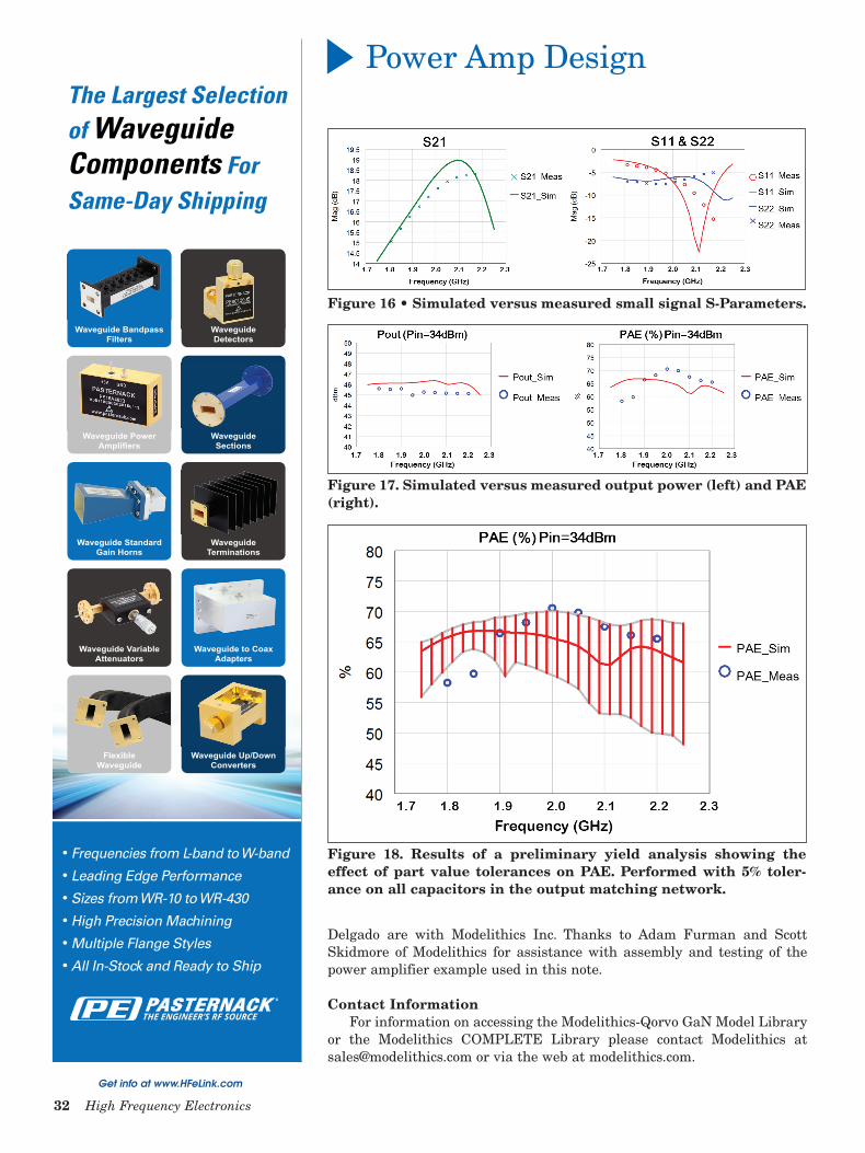
Figure 16 • Simulated versus measured small signal S-Parameters.
Figure 17. Simulated versus measured output power (left) and PAE (right).
Figure 18. Results of a preliminary yield analysis showing the effect of part value tolerances on PAE. Performed with 5% toler-ance on all capacitors in the output matching network.