Embed Size (px)
Citation preview

RSC Advances
PAPER
Publ
ishe
d on
13
Apr
il 20
15. D
ownl
oade
d by
Ren
ssel
aer
Poly
tech
nic
Inst
itute
on
29/0
4/20
15 1
7:45
:40.
View Article OnlineView Journal | View Issue
A simple growth
aDepartment of Physics, Applied Physics
Institute, 110 8th Street, Troy, New York
com; [email protected] of Chemistry and Chemical Bio
8th Street, Troy, New York 12180, USAcBrookhaven National Lab, Center for Funct
5000, Upton, New York 11973, USA
Cite this: RSC Adv., 2015, 5, 36129
Received 22nd March 2015Accepted 13th April 2015
DOI: 10.1039/c5ra05074j
www.rsc.org/advances
This journal is © The Royal Society of C
method for Nb2O5 films and theiroptical properties
J. K. Dash,*a L. Chen,a Michael R. Topka,b Peter H. Dinolfo,b L. H. Zhang,c
K. Kisslinger,c T.-M. Lua and G.-C. Wanga
A simple method for the synthesis of Nb2O5 films of thicknesses ranging from tens to several hundreds of
nanometers on amorphous silicon dioxide or quartz substrates is presented. Nb2O5 films were formed by
annealing the sputter deposited Nb films under an Ar flow and without oxygen plasma in a quartz tube
within a furnace at 850 �C. The structural, compositional, optical, and vibrational properties were
characterized by grazing incidence X-ray diffraction, transmission electron microscopy, X-ray
photoelectron spectroscopy, ultraviolet visible spectroscopy, and Raman scattering. Each of the Nb2O5
films is polycrystalline with an orthorhombic crystal structure. We observed vibrational modes including
longitudinal optical, transverse optical, and triply degenerate modes, and measured the indirect optical
band gap to be �3.65 eV. The transmittance spectrum of the �20 nm thick Nb2O5 film shows over 90%
transmittance below the band gap energy in the visible wavelength range and decreases to less than
20% in the ultraviolet regime. The optical properties of the films in the UV-vis range show potential
applications as UV detectors.
1. Introduction
Niobium oxides have attracted attention among researchers fortheir rich charge states, phases, morphologies, and associatedproperties. The number of charge states of niobium rangesfrom +2 to +4 to +5 for NbO, NbO2 and Nb2O5, respectively.These suboxides can be conductors, n-type semiconductors, orinsulators. Nb2O5 has the highest heat of formation (�1899.54 �8.37 kJ mol�1) compared with NbO2 (�792.87 � 6.28 kJ mol�1)and NbO (�407.94� 12.55 kJ mol�1)1 and is the most stable onceit is formed. Nb2O5 exists in various phases including thepseudohexagonal (TT-phase), orthorhombic (T-phase), andmonoclinic (H-phase). Various physical or chemical processingmethods have been developed to prepare Nb2O5 thin lms andnanostructures. Examples of Nb2O5 thin lm preparations arereactive sputtering of a Nb target in an Ar–O2 plasma on SiO2/Sisubstrates2,3 or in an atmosphere composed of oxygen andargon,4 pulsed laser deposition of Nb on Si followed by exposureto atmosphere,5 reactive RF magnetron sputtering of a Nb2O5
target on glass substrates,6 atomic layer deposition,7 and sol–geldip coating.8 The extended sol–gel method was also used toform nanocrystalline Nb2O5 lms.9 Other nanostructures
and Astronomy, Rensselaer Polytechnic
12180, USA. E-mail: jatiskumar@gmail.
logy, Rensselaer Polytechnic Institute, 110
ional Nanomaterials Bldg. 735, P.O. Box
hemistry 2015
synthesized by chemical processes in the form of nanowires,10–12
nanorods,13–15 nanotubes,16–18 nanobelts,19,20 nanopores,21
nanopowders,22 and nanohollow bers23 have been reported. Awide range of potential applications has been demonstrated:catalysis,24 gas sensors,12,21 electrochromic windows,25 photo-detectors,19 electron eld emitters,11 and solid oxide fuel cells.26
In this work we report a simple method to fabricate ultrathinNb2O5 lms by post annealing the magnetron sputtered Nb lms.We study their properties including structure, chemical composi-tion, optical transmittance and reection, optical bandgap, surfacemorphology, and vibrational modes. The characterization tech-niques used are grazing incidence X-ray diffraction (GIXRD),transmission electron microscopy (TEM), X-ray photoelectronspectroscopy (XPS), ultraviolet visible (UV-VIS) spectroscopy,atomic force microscopy (AFM), X-ray specular reectivity (XRR),and Raman scattering.
The advantages of our ultrathin Nb2O5 lm growth methodare (1) the oxide lm thickness can be controlled by the initialthickness of the Nb lm and the oxide lm is continuous, (2)there is no need to use the oxygen plasma, pulsed laser, orchemical precursors, but it only needs an Ar ow in the quartztube in a furnace, and (3) the optical properties includingtransmittance, reection and optical bandgap energy of 3.65 eVare suitable for UV detection.
2. Experimental
Ultrathin Nb lms of thicknesses 5, 10, 100, and 300 nm weredeposited by DCmagnetron sputter deposition on 300 nm thick
RSC Adv., 2015, 5, 36129–36139 | 36129

RSC Advances Paper
Publ
ishe
d on
13
Apr
il 20
15. D
ownl
oade
d by
Ren
ssel
aer
Poly
tech
nic
Inst
itute
on
29/0
4/20
15 1
7:45
:40.
View Article Online
SiO2 covered Si (001) substrates (of resistivity 0.001–0.005 ohmcm) and quartz slides (Structure Probe, Inc.). The base pressureof the sputter deposition chamber was�7.5� 10�7 Torr. The Argas ow rate was controlled at 2.01 standard cubic centimetersper minute (sccm) and the working pressure of Ar was set to 2.3mTorr. The power was set to 50 W. The Nb target (99.95%purity) was a 3 inch round disk and the distance from the targetsurface to the center of the substrate was �15 cm. The deposi-tion rate was �3.5 nm min�1. This deposition rate was cali-brated from the cross sectional image obtained from thescanning electron microscopy (SEM).
The Nb ultrathin lms on SiO2/Si and quartz substrates werethen placed in a quartz boat (100 � 45 � 20 mm) positioned atthe center of a 30 inch long quartz tube with outside and insidediameters of 59 and 55 mm, respectively. This quartz tube wasplaced inside a one zone furnace and then purged with anultrahigh purity Ar gas (99.999%) at a ow rate of 950 sccm.Aer 20 min of Ar purging, the Ar ow rate was reduced to 200sccm while the quartz boat was gradually heated up from roomtemperature to 850 �C in the furnace over about 80 min. Thetemperature was measured using a type K thermocouple withan accuracy of �5 �C. The boats were kept at 850 �C for 30 minbefore the furnace lament current was reduced to zero over 5–6min. The quartz tube then cooled down to room temperature inabout 120 min. Ar gas purging was continuous during the entireheating up and cooling down processes. The temperatureramping was managed using a Eurotherm 2116 PID program-mable temperature controller attached to the furnace. Thefurnace and Ar gas handling lines were placed inside a ventinghood. Fig. 1(a) shows a schematic of the sputter deposited Nblm on SiO2/Si. For optical measurements the Nb lms weresputter deposited on quartz substrates. Fig. 1(b) shows a TEMcross-sectional view of a Nb2O5 lm synthesized from a 300 nmthick Nb lm grown on a SiO2/Si (001) substrate that wasannealed at 850 �C for 30 min inside the quartz tube furnace.The uniform contrast areas near the bottom le are Si and SiO2.The area to the right of SiO2 is the Nb2O5 lm followed by a thinlayer of epoxy (M-bond) and a Pt layer. The 300 � 5 nm thick-ness of the SiO2 layer is in agreement with the vender's thick-ness specication. The thickness of the Nb2O5 lm is 800 � 20nm. This oxide layer is a result of the oxidation of the 300 nm
Fig. 1 (a) Schematic of sputtered Nb film on 300 nm thick amorphousSiO2 on 500 mm thick Si (001) substrate. The schematic is not to scale.(b) TEM cross section image of a synthesized Nb2O5/SiO2/Si (001)sample from 300 nm thick Nb film on SiO2/Si (001) after 850 �Cannealing for 30 min.
36130 | RSC Adv., 2015, 5, 36129–36139
thick Nb lm. Many grains with sizes on the order of hundredsnm to microns are seen.
Grazing incidence X-ray diffraction (GIXRD) theta–2theta (q–2q) scans were collected using a PANalytical X'Pert Pro diffrac-tometer to characterize the atomic structure and average grainsize of the Nb2O5 lms. A parallel X-ray beam generated from aparabolic mirror with a wavelength of 1.5405 A was incident onthe sample at a xed 1.5� grazing angle (u). A point detectorwith a 0.013� scanning step size and a 0.25 s counting time ateach step, was used to collect X-ray diffraction scans. During theGIXRD scan, the u was xed at 1.5� while the 2q was varied. Thedetector scanned over 2q in the scattering plane while thesource and sample stage were xed. The detector was scannedin the scattering plane that contains the incident X-ray and thesurface normal.
For the TEM sample, a thin layer of epoxy (M-bond) wasapplied to the surface of the Nb2O5 lm. A sacricial Pt layer wasdeposited on the surface of the epoxy layer for focused ion beam(FIB)/scanning electron microscopy (SEM) sample preparation.The sample was then thinned by FIB milling using energeticgallium ions. The thinned sample was mounted on a liquidnitrogen cooled sample stage to minimize the sample'smechanical driing. A 200 keV energy electron beam was usedto obtain the TEM (JEOL 2100 F) bright eld images, highresolution images, and electron diffraction patterns.
X-ray photoelectron spectroscopy (XPS) was used to deter-mine the near surface composition. The nearly monochromaticX-ray Mg K-alpha source (PHI model 04-151) had a primaryenergy of 1253.6 eV. The X-ray source was operated at 270 Wwith a 10 kV high-voltage bias and an emission current of 27mA. A double pass cylindrical mirror energy analyzer (PHImodel 15-255G) in a high vacuum chamber was used to detectthe emitted electrons from the sample surface. A high-resolution spectrum was averaged from 40 repeated scans at apassing energy of 50 eV. The energy resolution of the analyzer atthis passing energy is about 0.7 eV. The energy step size (0.08eV) used to scan Nb and O peaks is smaller than 0.7 eV in orderto provide a good relative resolution, dened as R ¼ DE/Eo,where DE is the passing energy and Eo is the kinetic energy of apeak position.27
UV-visible reectance and transmission spectra werecollected to determine the optical band gap of the ultrathinNb2O5 lms on quartz. The spectra were obtained from aPerkin-Elmer Lambda 950 UV/VIS Spectrometer. The trans-mission spectra were obtained with the slides held normal tothe incident light beam in air and were corrected for the quartzbackground. Specular reectance spectra were obtained at anear-normal incidence angle of 6�.
The AFM surface morphology images were collected using aPSI XE100 in non-contact mode. The HI'RES-C14/CR-AU AFMtip used has a tip radius of �1 nm, a force constant of 5 N m�1
and a resonant frequency of 160 kHz.X-ray reectivity (XRR) scan obtained for the Nb2O5 lms
grown on quartz were used to determine thickness, surfaceroughness and density. XRR scans were taken with a Bruker D8Discover X-ray Diffractometer using a 2-circle q/2q goniometer, acentric Eulerian cradle, and a sealed copper tube X-ray source
This journal is © The Royal Society of Chemistry 2015
Paper RSC Advances
Publ
ishe
d on
13
Apr
il 20
15. D
ownl
oade
d by
Ren
ssel
aer
Poly
tech
nic
Inst
itute
on
29/0
4/20
15 1
7:45
:40.
View Article Online
(Cu Ka, l ¼ 1.54 A) operated at 40 kV. A 40 mm Gobel colli-mating mirror and a four-position rotary absorber were used forthe incident beam with attenuations of approximately 1 : 1,1 : 10, 1 : 100 and 1 : 1000. Slits of 1.0 mm and 0.2 mm wereused before and aer the rotary absorber, respectively. A knifeedge was employed to optimize the measurements. Data werecollected at grazing incidence angles ranging from 0 to 5� at0.01� increments and repeated scans were collected and aver-aged until the desired signal to noise level was reached.
Raman spectra that provide vibrational mode informationwere collected using a Witec Alpha 300 confocal Ramanmicroscope. The laser wavelength and power used for themeasurements of the Raman spectra were 532.1 nm and 17mW, respectively. A 100� objective lens produced a spot size of�721 nm (¼1.22� wavelength/numerical aperture of 0.9 for the100� objective lens). The spectral resolution and step size usedin Raman scattering data collection were each 0.02 cm�1.
3. Results3.1. Structural property
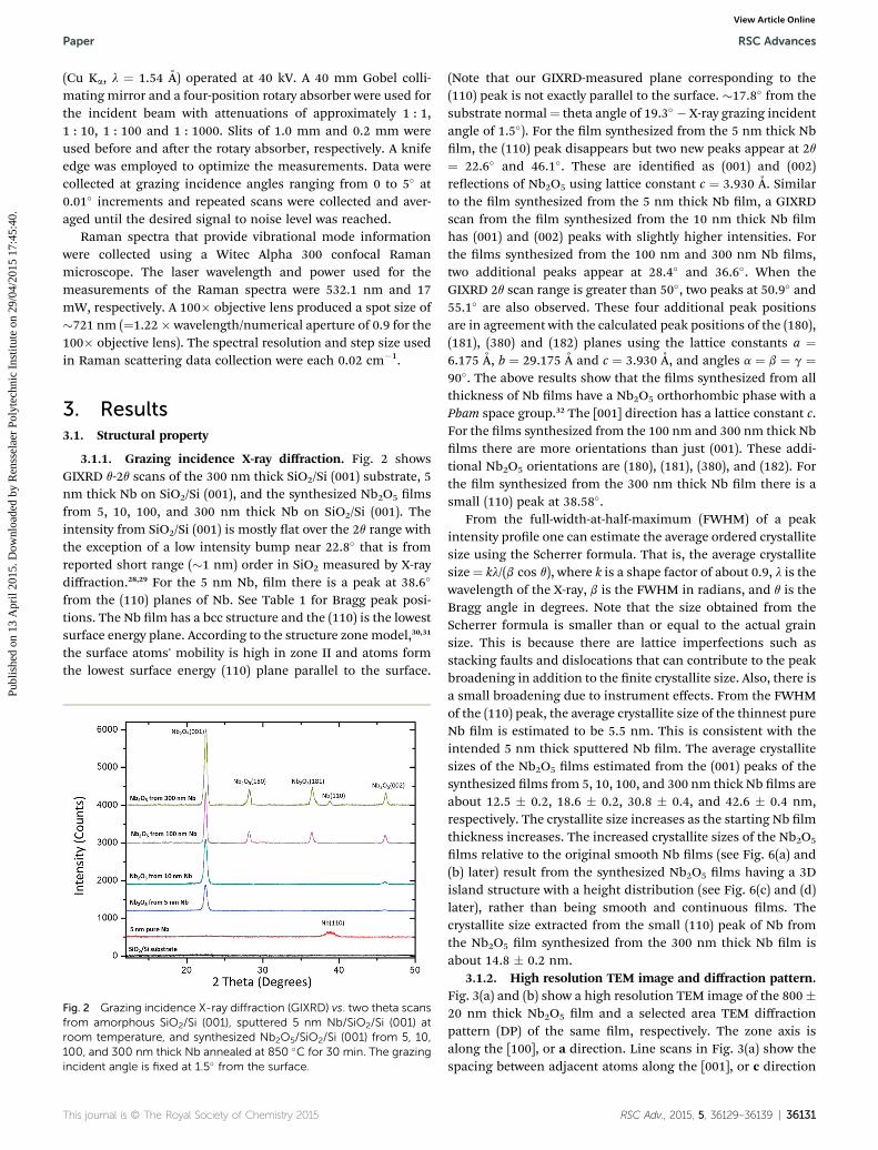
3.1.1. Grazing incidence X-ray diffraction. Fig. 2 showsGIXRD q-2q scans of the 300 nm thick SiO2/Si (001) substrate, 5nm thick Nb on SiO2/Si (001), and the synthesized Nb2O5 lmsfrom 5, 10, 100, and 300 nm thick Nb on SiO2/Si (001). Theintensity from SiO2/Si (001) is mostly at over the 2q range withthe exception of a low intensity bump near 22.8� that is fromreported short range (�1 nm) order in SiO2 measured by X-raydiffraction.28,29 For the 5 nm Nb, lm there is a peak at 38.6�
from the (110) planes of Nb. See Table 1 for Bragg peak posi-tions. The Nb lm has a bcc structure and the (110) is the lowestsurface energy plane. According to the structure zone model,30,31
the surface atoms' mobility is high in zone II and atoms formthe lowest surface energy (110) plane parallel to the surface.
Fig. 2 Grazing incidence X-ray diffraction (GIXRD) vs. two theta scansfrom amorphous SiO2/Si (001), sputtered 5 nm Nb/SiO2/Si (001) atroom temperature, and synthesized Nb2O5/SiO2/Si (001) from 5, 10,100, and 300 nm thick Nb annealed at 850 �C for 30 min. The grazingincident angle is fixed at 1.5� from the surface.
This journal is © The Royal Society of Chemistry 2015
(Note that our GIXRD-measured plane corresponding to the(110) peak is not exactly parallel to the surface. �17.8� from thesubstrate normal¼ theta angle of 19.3� � X-ray grazing incidentangle of 1.5�). For the lm synthesized from the 5 nm thick Nblm, the (110) peak disappears but two new peaks appear at 2q¼ 22.6� and 46.1�. These are identied as (001) and (002)reections of Nb2O5 using lattice constant c ¼ 3.930 A. Similarto the lm synthesized from the 5 nm thick Nb lm, a GIXRDscan from the lm synthesized from the 10 nm thick Nb lmhas (001) and (002) peaks with slightly higher intensities. Forthe lms synthesized from the 100 nm and 300 nm Nb lms,two additional peaks appear at 28.4� and 36.6�. When theGIXRD 2q scan range is greater than 50�, two peaks at 50.9� and55.1� are also observed. These four additional peak positionsare in agreement with the calculated peak positions of the (180),(181), (380) and (182) planes using the lattice constants a ¼6.175 A, b ¼ 29.175 A and c ¼ 3.930 A, and angles a ¼ b ¼ g ¼90�. The above results show that the lms synthesized from allthickness of Nb lms have a Nb2O5 orthorhombic phase with aPbam space group.32 The [001] direction has a lattice constant c.For the lms synthesized from the 100 nm and 300 nm thick Nblms there are more orientations than just (001). These addi-tional Nb2O5 orientations are (180), (181), (380), and (182). Forthe lm synthesized from the 300 nm thick Nb lm there is asmall (110) peak at 38.58�.
From the full-width-at-half-maximum (FWHM) of a peakintensity prole one can estimate the average ordered crystallitesize using the Scherrer formula. That is, the average crystallitesize¼ kl/(b cos q), where k is a shape factor of about 0.9, l is thewavelength of the X-ray, b is the FWHM in radians, and q is theBragg angle in degrees. Note that the size obtained from theScherrer formula is smaller than or equal to the actual grainsize. This is because there are lattice imperfections such asstacking faults and dislocations that can contribute to the peakbroadening in addition to the nite crystallite size. Also, there isa small broadening due to instrument effects. From the FWHMof the (110) peak, the average crystallite size of the thinnest pureNb lm is estimated to be 5.5 nm. This is consistent with theintended 5 nm thick sputtered Nb lm. The average crystallitesizes of the Nb2O5 lms estimated from the (001) peaks of thesynthesized lms from 5, 10, 100, and 300 nm thick Nb lms areabout 12.5 � 0.2, 18.6 � 0.2, 30.8 � 0.4, and 42.6 � 0.4 nm,respectively. The crystallite size increases as the starting Nb lmthickness increases. The increased crystallite sizes of the Nb2O5
lms relative to the original smooth Nb lms (see Fig. 6(a) and(b) later) result from the synthesized Nb2O5 lms having a 3Disland structure with a height distribution (see Fig. 6(c) and (d)later), rather than being smooth and continuous lms. Thecrystallite size extracted from the small (110) peak of Nb fromthe Nb2O5 lm synthesized from the 300 nm thick Nb lm isabout 14.8 � 0.2 nm.
3.1.2. High resolution TEM image and diffraction pattern.Fig. 3(a) and (b) show a high resolution TEM image of the 800�20 nm thick Nb2O5 lm and a selected area TEM diffractionpattern (DP) of the same lm, respectively. The zone axis isalong the [100], or a direction. Line scans in Fig. 3(a) show thespacing between adjacent atoms along the [001], or c direction
RSC Adv., 2015, 5, 36129–36139 | 36131

Table 1 Bragg peak and average ordered crystallite size from XRD and film's roughness parameters including surface width, correlation lengthand roughness exponent from AFM
Sample(nm)
GIXRD AFM
Orientation(XRD Bragg peak)
Ave. orderedcrystalline size (nm)
Surfacewidth u (nm)
Correlationlength x (nm)
Roughnessexponent a
5 nm Nb 110 (38.6�) 5.5 � 0.1 — — —Nb2O5
synthesizedlms from
5 nm Nb 001 (22.6�), 002 (46.1�) 12.5 � 0.2 3.6 � 0.2 84 � 2 0.7810 nm Nb 001 (22.6�), 002 (46.1�) 18.6 � 0.4 3.8 � 0.2 91 � 2 0.72300 nm Nb 001 (22.6�), 002 (46.1�),
180 (28.4�), 181 (36.6�),380 (50.9�), 182 (55.1�)
42.6 � 0.4 17.4 � 0.3 193 � 7 0.61
RSC Advances Paper
Publ
ishe
d on
13
Apr
il 20
15. D
ownl
oade
d by
Ren
ssel
aer
Poly
tech
nic
Inst
itute
on
29/0
4/20
15 1
7:45
:40.
View Article Online
is uniform with average measured spacing of c ¼ 0.390 � 0.010nm. However, the spacing among the adjacent atoms in the[010], or b direction is not as uniform. First, the atoms are notall aligned in a straight line along the b direction; some deviatefrom the straight line. Secondly, the spacing between twoadjacent atoms also varies. This is consistent with the spacingvariation of atomic positions, as determined from X-raydiffraction.32 The lattice spacing along the b direction deter-mined from X-ray peak positions such as (180) and (181) dis-cussed in section 3.1.1 is 2.9175 nm. We have measured therepeated equivalent spacing (unit length) over hundreds of nmalong the b direction using ImageJ soware to analyze the highresolution TEM image and have obtained an average spacing of2.83 � 0.05 nm labeled as b between the two arrows shown inFig. 3(a). To determine the unit length along the b directionmore accurately we use the diffraction pattern shown inFig. 3(b) next.
The lengths of the reciprocal unit vectors c* and b* aremeasured from the spots in the DP shown in Fig. 3(b). Wemeasured the reciprocal length b* between the 2nd order spots inthe positive and negative b* directions, or 4b*, and then dividedby 4 (the 000 spot is too strong and the TEM beam stopper blocksthe spot). The measured values are c*¼ 2.64� 0.01 nm�1 and b*¼ 0.357 � 0.005 nm�1. The inverses of c* and b* correspond to
Fig. 3 (a) High resolution real space TEM image (scale bar is 2 nm) and (bfrom 300 nm thick Nb grown on 300 nm thick SiO2/Si (001) and anneal
36132 | RSC Adv., 2015, 5, 36129–36139
real space spacings cz 0.378 nm and bz 2.80 nm, respectively.These are in reasonable agreement with the measured real spaceunit lengths c and b shown in Fig. 3(a) as well lattice constantsobtained from X-ray diffraction. Miller indices of the strongerdiffraction spots are labeled. All reciprocal lattice vector lengthsG(hkl) match well to the real space spacings dhkl through dhkl ¼ 1/G(hkl). The fast Fourier transform of the real space image shownin Fig. 3(a) using ImageJ soware33 gives a DP in agreement withthe observed DP. The real space high resolution image in Fig. 3(a)shows that many stacking faults exist along the b direction. Thestacking faults give raise to the elongated diffraction spots alongthe b* direction seen in Fig. 3(b). Note the lower resolution brighteld TEM image shown in Fig. 1(b) does not reveal these stackingfaults. The grain size seen in TEM is much larger than the crys-tallite size determined from the FWHM of XRD peak.
Other high resolution TEM images of the Nb2O5 lm and thecorresponding selected area TEM DPs were also measured froma grain with the zone axis along the [001], or c direction so thatthe [100], or a direction is parallel to the high resolution image.The measured unit vector length, a from the real space highresolution TEM image and TEM DP are consistent with thevalue of 0.6168 nm determined from the (180) peak in Section3.1.1.
) TEM diffraction pattern (scale bar is 1 nm�1) of Nb2O5 film synthesizeded at 850 �C for 30 min.
This journal is © The Royal Society of Chemistry 2015
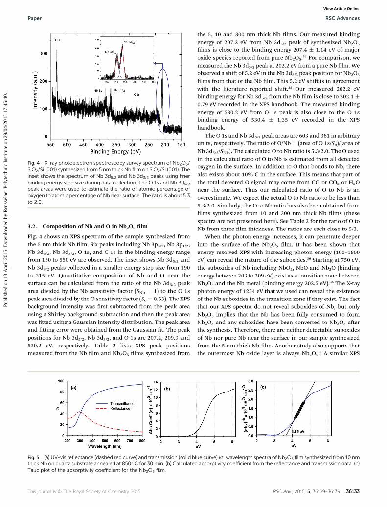
Fig. 4 X-ray photoelectron spectroscopy survey spectrum of Nb2O5/SiO2/Si (001) synthesized from 5 nm thick Nb film on SiO2/Si (001). Theinset shows the spectrum of Nb 3d5/2 and Nb 3d3/2 peaks using finerbinding energy step size during data collection. The O 1s and Nb 3d5/2peak areas were used to estimate the ratio of atomic percentage ofoxygen to atomic percentage of Nb near surface. The ratio is about 5.3to 2.0.
Paper RSC Advances
Publ
ishe
d on
13
Apr
il 20
15. D
ownl
oade
d by
Ren
ssel
aer
Poly
tech
nic
Inst
itute
on
29/0
4/20
15 1
7:45
:40.
View Article Online
3.2. Composition of Nb and O in Nb2O5 lm
Fig. 4 shows an XPS spectrum of the sample synthesized fromthe 5 nm thick Nb lm. Six peaks including Nb 3p3/2, Nb 3p1/2,Nb 3d5/2, Nb 3d3/2, O 1s, and C 1s in the binding energy rangefrom 150 to 550 eV are observed. The inset shows Nb 3d5/2 andNb 3d3/2 peaks collected in a smaller energy step size from 190to 215 eV. Quantitative composition of Nb and O near thesurface can be calculated from the ratio of the Nb 3d5/2 peakarea divided by the Nb sensitivity factor (SNb ¼ 1) to the O 1speak area divided by the O sensitivity factor (So ¼ 0.63). The XPSbackground intensity was rst subtracted from the peak areausing a Shirley background subtraction and then the peak areawas tted using a Gaussian intensity distribution. The peak areaand tting error were obtained from the Gaussian t. The peakpositions for Nb 3d5/2, Nb 3d3/2, and O 1s are 207.2, 209.9 and530.2 eV, respectively. Table 2 lists XPS peak positionsmeasured from the Nb lm and Nb2O5 lms synthesized from
Fig. 5 (a) UV-vis reflectance (dashed red curve) and transmission (solid blthick Nb on quartz substrate annealed at 850 �C for 30min. (b) CalculatedTauc plot of the absorptivity coefficient for the Nb2O5 film.
This journal is © The Royal Society of Chemistry 2015
the 5, 10 and 300 nm thick Nb lms. Our measured bindingenergy of 207.2 eV from Nb 3d5/2 peak of synthesized Nb2O5
lms is close to the binding energy 207.4 � 1.14 eV of majoroxide species reported from pure Nb2O5.34 For comparison, wemeasured the Nb 3d5/2 peak at 202.2 eV from a pure Nb lm. Weobserved a shi of 5.2 eV in the Nb 3d5/2 peak position for Nb2O5
lms from that of the Nb lm. This 5.2 eV shi is in agreementwith the literature reported shi.35 Our measured 202.2 eVbinding energy for Nb 3d5/2 from the Nb lm is close to 202.1 �0.79 eV recorded in the XPS handbook. The measured bindingenergy of 530.2 eV from O 1s peak is also close to the O 1sbinding energy of 530.4 � 1.35 eV recorded in the XPShandbook.
The O 1s and Nb 3d5/2 peak areas are 603 and 361 in arbitraryunits, respectively. The ratio of O/Nb ¼ (area of O 1s/So)/(area ofNb 3d5/2/SNb). The calculated O to Nb ratio is 5.3/2.0. The O usedin the calculated ratio of O to Nb is estimated from all detectedoxygen in the surface. In addition to O that bonds to Nb, therealso exists about 10% C in the surface. This means that part ofthe total detected O signal may come from CO or CO2 or H2Onear the surface. Thus our calculated ratio of O to Nb is anoverestimate. We expect the actual O to Nb ratio to be less than5.3/2.0. Similarly, the O to Nb ratio has also been obtained fromlms synthesized from 10 and 300 nm thick Nb lms (thesespectra are not presented here). See Table 2 for the ratio of O toNb from three lm thickness. The ratios are each close to 5/2.
When the photon energy increases, it can penetrate deeperinto the surface of the Nb2O5 lm. It has been shown thatenergy resolved XPS with increasing photon energy (100–1600eV) can reveal the nature of the suboxides.36 Starting at 750 eV,the suboxides of Nb including NbO2, NbO and Nb2O (bindingenergy between 203 to 209 eV) exist as a transition zone betweenNb2O5 and the Nb metal (binding energy 202.5 eV).36 The X-rayphoton energy of 1254 eV that we used can reveal the existenceof the Nb suboxides in the transition zone if they exist. The factthat our XPS spectra do not reveal suboxides of Nb, but onlyNb2O5 implies that the Nb has been fully consumed to formNb2O5 and any suboxides have been converted to Nb2O5 aerthe synthesis. Therefore, there are neither detectable suboxidesof Nb nor pure Nb near the surface in our sample synthesizedfrom the 5 nm thick Nb lm. Another study also supports thatthe outermost Nb oxide layer is always Nb2O5.5 A similar XPS
ue curve) vs.wavelength spectra of Nb2O5 film synthesized from 10 nmabsorptivity coefficient from the reflectance and transmission data. (c)
RSC Adv., 2015, 5, 36129–36139 | 36133

Fig. 6 Atomic force microscopy images (5 mm � 5 mm) and histograms of (a) 5 nm thick Nb film and (b) 10 nm thick Nb film on SiO2/Si (001)before synthesis. AFM images (1 mm � 1 mm) of Nb2O5/SiO2/Si (001) synthesized from (c) 5 nm thick Nb film and (d) 10 nm thick Nb film.
RSC Advances Paper
Publ
ishe
d on
13
Apr
il 20
15. D
ownl
oade
d by
Ren
ssel
aer
Poly
tech
nic
Inst
itute
on
29/0
4/20
15 1
7:45
:40.
View Article Online
spectrum shows that no suboxide exists in the sample synthe-sized from the 10 nm thick Nb lm. In contrast, for the lmsynthesized from the 300 thick Nb lm under the same condi-tion of 850 �C annealing for 30 min, there is pure Nb le nearthe surface. This implies that within the annealing temperatureand time, the oxidation process has not consumed all the Nb inthe 300 nm thick Nb lm and converted it to Nb2O5. This is whya small (110) peak from pure Nb was observed in XRD.
3.3. Optical bandgap of Nb2O5 lm on quartz measuredfrom UV-visible absorption
Fig. 5(a) shows the UV-vis reectance and transmission spectraof the Nb2O5 lm synthesized from the 10 nm thick Nb lm onquartz. These spectra have been corrected for the quartz back-ground measured from an annealed quartz substrate without
Table 2 Measured binding energies of Nb in Nb film and Nb in Nb2O5 fi
Samples
Binding energy ofNb in Nb lm (eV) Bindi
Nb 3d5/2 Nb 3d3/2 Nb 3d
5 nm Nb 202.2 205.0 —Nb2O5 synthesized from 5 nm Nb — — 207.2
10 nm Nb — — 207.2300 nm Nb — 204.9 207.2
36134 | RSC Adv., 2015, 5, 36129–36139
the Nb lm. A small bump exists in the reectance spectrumaround a wavelength of 300 nm. The transmittance spectrumshows a high transmittance in the visible wavelength range,which decreases in the UV wavelength range. The resultingabsorptivity coefficient, a37 of the Nb2O5 lm (Fig. 5(b)) shows asharp onset around 4 eV. The optical bandgap of the Nb2O5 lmis determined from the experimental UV-vis absorption spectravia the Tauc method38 by extrapolating the linear portion of the(ahn)1/2 vs. hn plot to the intercept, where a is the absorptioncoefficient, hn is the photon energy, and the exponent 1/2 is foran indirect bandgap. Fig. 5(c) shows the Tauc analysis for theNb2O5 lm synthesized from the 10 nm thick Nb lm on quartzwhich gives an optical bandgap of 3.65 � 0.02 eV (¼340 nm).
The bandgap for bulk Nb2O5 is about 3.4 eV.17 Experimen-tally measured bandgaps for lms range from 3 to over 4 eVdepending on the structural phase, grain size, and morphology
lms from XPS. The “—“ means no peak
ng energy of major species in Nb2O5 lms (eV)Ratio of Oto Nb5/2 Nb 3d3/2 C 1s Nb 3p3/2 Nb 3p1/2 O 1s
— 285 — — 530.1209.9 285 365.4 381.2 530.2 5.30/2209.9 285 365.4 381.2 530.2 5.31/2209.9 285 365.4 381.2 530.2 5.34/2
This journal is © The Royal Society of Chemistry 2015

Fig. 7 X-ray specular reflectivity curve (black filled circles) and fittedmodel (red curve) vs. momentum transfer q for the Nb2O5 filmsynthesized from 10 nm thick Nb film on quartz substrate.
Paper RSC Advances
Publ
ishe
d on
13
Apr
il 20
15. D
ownl
oade
d by
Ren
ssel
aer
Poly
tech
nic
Inst
itute
on
29/0
4/20
15 1
7:45
:40.
View Article Online
of the Nb2O5 lm as well as the exponent used in the Taucplot.8,23 Our measured bandgap of 3.65 eV is close to thatmeasured from single crystalline Nb2O5 nanorods grown byhydrothermal technique18 using UV-vis (note that the exponentof ahn used in that work was 2 instead of 1/2). Our value is alsocomparable to the value of 3.7 eV determined for pulsed laserdeposited Nb lm exposed in air and measured by ultravioletphotoelectron spectroscopy.5 Density functional theory (DFT)calculations of Nb2O5 indicate that Nb2O5 is an indirectbandgap semiconductor with a bandgap of 2.55 eV. Theunderestimation by DFT calculations is typical due to thediscontinuity of exchange correlation energy.5
The reectance and transmission spectra of Nb2O5 lmsynthesized from 10 nm thick Nb lm shown in Fig. 5 do nothave the interference feature as compared with those of the fewhundreds of nm thick Nb2O5 samples grown on Si substrate orglass substrates reported in previous work.3,6 Unlike theirthicker lms, our lm has a much smaller dimension than theUV-vis wavelength used in the measurement and the waveinterference from the lm and substrate interface does notoccur.
3.4. Film morphology and roughness
3.4.1. Atomic force microscopy. Fig. 6 shows AFM imagesand height histograms of the 5 and 10 nm thick Nb lms onSiO2/Si (001), and the Nb2O5 lms synthesized from the 5 and 10nm thick Nb lms on SiO2/Si (001) substrates. The 5 and 10 nmNb lms shown in Fig. 6(a) and (b) are smooth and almostfeatureless with root mean square (RMS) roughnesses in thesub-nm range (�0.6 nm). In contrast, the synthesized Nb2O5
lms shown in Fig. 6(c) and (d) have island-like features. Theheight histograms shown below the AFM images range from0 to 25 nmwith a peak around 12 nm and 0 to 30 nmwith a peakaround 17 nm for the Nb2O5 lms synthesized from the 5 and 10nm thick Nb lms, respectively.
We analyzed the two-dimensional height–height correlationfunction, H(r) from these AFM images to extract the roughnessparameters including the vertical surface width, u (or RMSroughness), lateral correlation length, x, and roughness
This journal is © The Royal Society of Chemistry 2015
exponent, a.39–41 H(r) is dened as H(r) ¼ h[h(r) – h(0)]2i, whereh(r) is the surface height at position r and h(0) is the surfaceheight at a reference position r ¼ 0. Surface width, u is thesquare root of h[h(r) � hhi]2i, where hhi is the average height ofthe surface. u describes the surface roughness at largedistances. The lateral correlation length, x describes the“wavelength” of the surface uctuations. For large r, the surfaceheight uctuations should not be correlated, and H(r) ¼ 2u2.For small r, the surface height–height correlation has theasymptotic form H(r) � r2a, where a is the local roughnessexponent. a describes how “wiggly” the surface is and has avalue 0 < a # 1, with 1 being the smoothest.
To perform the height–height correlation function analysis,one needs to be aware of the sampling induced oscillation.42 Ifthe sampling size L is sufficiently larger than the correlationlength x, then the oscillation will diminish when (x/L)d/2 � 1,where d is a dimension, and when a large number of imagesfrom a rough surface are averaged. If the oscillations do notdiminish under these conditions, then the surface is a moun-ded rough surface. Table 1 lists the height–height correlationfunction analyses of ten AFM images from each of these Nb2O5
lms synthesized from the 5, 10 and 300 nm thick Nb lms.Table 1 indicates that the vertical surface width u increasesfrom 3.6 � 0.2 nm to 17.4 � 0.3 nm, and the lateral correlationlength x increases from 84 � 2 nm to 193 � 7 nm. The localroughness parameter a decreases from 0.78 to 0.61 andbecomes more wiggly as the lm thickness increases. The 1 � 1mm sampling size L of the ten AFM images and the �90 nm sizeof x, which gives (x/L)d/2 z 0.09 for d ¼ 2. Aer averaging 10images, the height–height correlation function still has obviousoscillations with regular separation. This is consistent withresults obtained for a rough surface with mounds.42 Thesemounds are seen as islands in the AFM images shown inFig. 6(c) and (d).
From Table 1, the lateral correlation length x extracted fromAFM is larger than the average grain size obtained from GIXRD.This implies that there is more than one grain in eachmorphological feature. For the Nb2O5 lm synthesized from the300 nm thick Nb lm, the value of x is of the same order ofmagnitude as the lateral size obtained from the TEM crosssection view shown in Fig. 1(b).
3.4.2. X-ray specular reectivity. X-ray specular reectivity(XRR) curves were obtained to probe the thickness, roughness,and density of the niobium oxide lm on quartz. X-rays areincident at a grazing angle and reect off from various inter-faces of a thin lm resulting in an interference pattern as theangle of incidence changes. Fig. 7 shows the XRR curve vs.momentum transfer, q (A�1) resulting from the Nb2O5 lmsynthesized from the 10 nm Nb lm on a quartz substratefollowing an annealing at 850 �C. The dependence of theoscillatory reectivity observed in the interference pattern, orKiessig fringes, on thickness can be described by the Braggequation. A more detailed description can be found else-where.43,44 The XRR prole was modeled as a thin Nb2O5 lm ontop of a SiO2 substrate using the LEPTOS soware suite fromBruker AXS. The model was tted to the data using the
RSC Adv., 2015, 5, 36129–36139 | 36135

Fig. 8 Raman shift spectra measured at room temperature. (a) SiO2/Si (001) that was annealed at 850 �C for 30 min and cooled down to roomtemperature, (b) Nb2O5/SiO2/Si (001) synthesized from 5 nm thick Nb film, (c) difference spectrum of (b) minus (a) to remove Si substratecontribution. Peak fit of difference spectrum of Nb2O5/SiO2/Si (001) synthesized from 5 nm thick Nb film in three Raman shift regimes (d) 100–500 cm�1, (e) 500–800 cm�1, and (f) 800–1100 cm�1.
RSC Advances Paper
Publ
ishe
d on
13
Apr
il 20
15. D
ownl
oade
d by
Ren
ssel
aer
Poly
tech
nic
Inst
itute
on
29/0
4/20
15 1
7:45
:40.
View Article Online
thickness of the niobium oxide lm, and the roughness anddensity of both the lm and substrate as variables.
The Nb2O5 lm thickness was determined to be 22.57 � 0.09nm with a surface roughness of 2.2 � 0.3 nm from the XRRcurve. This thickness is higher than the histogram shown inFig. 6(b) probably due to the AFM tip size effect when imagingthe depth of closely spaced small features. The density wasdetermined to be 5.34 � 0.07 g cm�3, which agrees, approxi-mately, with the orthorhombic density of 5.24 g cm�3 (ref. 32)and is slightly higher than the TT and T phases of Nb2O5, of 4.99and 5.00 g cm�3, respectively.45 Using the density of the 10 nmNb lm thickness, and considering the stoichiometric ratio inmass change by converting Nb to Nb2O5 (2 Nb + 2.5 O2 /
Nb2O5), we can estimate the expected density of the 22 nm thickNb2O5 lm to be 5.43 g cm�3.
3.5. Vibrational modes of Nb2O5 lms from Raman spectra
Fig. 8 shows three Raman spectra: (a) the reference spectrumof a bare SiO2 covered Si (001) substrate aer 850 �Cannealing for 30 min; (b) the spectrum of the Nb2O5 lmsynthesized from the 5 nm thick Nb lm; (c) the differencebetween the Nb2O5 lm synthesized from the 5 nm thick Nb
36136 | RSC Adv., 2015, 5, 36129–36139
lm and the reference spectrum. The reference spectrum inFig. 8(a) shows two Si peaks, a sharp peak around 521 cm�1
and a broad peak around 972 cm�1. Both Si peaks also showup with high intensity in the Raman spectrum of the Nb2O5
lm shown in Fig. 8(b). For the 532 nm laser wavelength thatwe used in our experiment, the optical penetration depth isabout 0.7 mm and the photon energy is 2.33 eV, which ishigher than the Si bandgap of 1.11 eV. Raman resonances46
occur at 521 cm�1 and 972 cm�1 as shown in Fig. 8(a). Inorder to remove the observed enhancement effect in Ramanintensity from the Si (001) substrate when a 532 nm incidentlaser wavelength is used, we subtracted the reference spec-trum shown in Fig. 8(a) from the spectrum shown in Fig. 8(b).The difference spectrum shown in Fig. 8(c) has ve distinctRaman peaks at 238, 304, 647, 695, and 993 cm�1.
Among the ve peaks, the full-width-at-half-maximum(FWHM) of the Raman peaks in the difference spectrumFig. 8(c) varies from sharp to broad. The broad peak may containmore than one peak. Using Origin peak t soware we have ttedthe broad peaks and obtained extra peaks with the coefficient ofdetermination (goodness of t)¼ 0.992. The positions of peaks inthe Raman difference spectra from our Nb2O5 lms synthesized
This journal is © The Royal Society of Chemistry 2015
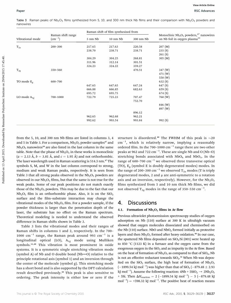
Table 3 Raman peaks of Nb2O5 films synthesized from 5, 10, and 300 nm thick Nb films and their comparison with Nb2O5 powders andnanowires
Vibrational modeRaman shi range(cm�1)
Raman shi of lm synthesized fromMonoclinic Nb2O5 powders,
47 nanowireson Nb foil in oxygen plasma105 nm Nb 10 nm Nb 300 nm Nb
T2m 200–300 217.65 217.63 220.58 207 (M)238.70 238.71 238.71 235 (S)
261 (S)304.29 304.25 268.81 305 (M)311.96 312.14 301.51324.23 324.22 359.27
T2g 350–560 470.51 347 (W)471 (W)550 (W)
TO mode Eg 600–700 632 (S)647.65 647.65 647.24 647 (S)666.88 666.85 682.63 659 (S)695.72 695.75 674 (S)
LO mode A1g 700–1000 722.79 725.23 707.47 760 (W)752.70
846 (W)897 (W)
896.12962.65 962.68 962.21992.62 993.54 993.84 992 (S)
Paper RSC Advances
Publ
ishe
d on
13
Apr
il 20
15. D
ownl
oade
d by
Ren
ssel
aer
Poly
tech
nic
Inst
itute
on
29/0
4/20
15 1
7:45
:40.
View Article Online
from the 5, 10, and 300 nm Nb lms are listed in columns 3, 4and 5 in Table 3. For a comparison, Nb2O5 powder samples47 andNb2O5 nanowires10 are also listed in the last column in the sametable. Note that the phase of Nb2O5 in these works is monoclinic(a ¼ 2.13 A, b ¼ 3.81 A, and c ¼ 1.95 A) and not orthorhombic.The laser wavelength used in Raman scattering is 514.5 nm.47 Thesymbols S, M, and W in the last column correspond to strong,medium and weak Raman peaks, respectively. It is seen fromTable 3 that all strong peaks observed in the Nb2O5 powders areobserved in our Nb2O5 lms, but that the same is not true for theweak peaks. Some of our peak positions do not match exactlythose of the Nb2O5 powders. This may be due to the fact that ourNb2O5 lm is an orthorhombic phase. Also, it is on the SiO2
surface and the lm–substrate interaction may change thevibrational modes of the Nb2O5 lm. For a powder sample, if thepowder thickness is larger than the penetration depth of thelaser, the substrate has no effect on the Raman spectrum.Theoretical modeling is needed to understand the observeddifference in Raman shis shown in Table 3.
Table 3 lists the vibrational modes and their ranges ofRaman shis in columns 1 and 2, respectively. In the 700–1000 cm�1 range, the Raman peak around 993 cm�1 is alongitudinal optical (LO), A1g mode using Mullikensymbols.11,48 This vibration is most prominent in oxidesystems. It is a symmetric single stretching vibration mode(symbol A) of Nb and O double bond (Nb]O) relative to theprinciple rotational axis (symbol 1) and an inversion throughthe center of the molecule (symbol g). This stretching modehas a short bond and is also supported by the DFT calculationresult described previously.49 This peak is also sensitive toordering. The peak intensity is either low or zero if the
This journal is © The Royal Society of Chemistry 2015
structure is disordered.48 The FWHM of this peak is �20cm�1, which is relatively narrow, implying a reasonablyordered lm. In the 700–1000 cm�1 range there are two otherpeaks at 962 and 722 cm�1. These are single Nb and O (Nb–O)stretching bonds associated with NbO6 and NbO4. In therange of 600–700 cm�1 we observed three transverse optical(TO), Eg (symbol E is doubly degenerated modes) modes. Inthe range of 200–300 cm�1 we observed T2m modes (T is triplydegenerated modes, 2 and m are anti-symmetric to a rotationaxis and an inversion, respectively). However, for the Nb2O5
lms synthesized from 5 and 10 nm thick Nb lms, we didnot observed T2g modes in the range of 350–550 cm�1.
4. Discussions4.1. Formation of Nb2O5 lms in Ar ow
Previous ultraviolet photoemission spectroscopy studies of oxygenadsorption on Nb (110) surface at 300 K in ultrahigh vacuumshowed that oxygen molecules dissociated and chemisorbed onthe Nb (110) surface. NbO and NbO2 formed initially as protectivelayers and then Nb2O5 formed aer heavy oxidation.50 In our case,the sputtered Nb lms deposited on SiO2/Si (001) were heated upto 850 �C (1123 K) in a furnace and the oxygen came from theexogenous oxygen in the SiO2 and as impurity in the Ar ow. Basedon the heat of formation of Nb2O5 as compared to that of SiO2, Nbis not an effective reductant towards SiO2.51 When Nb was depos-ited on the SiO2 surface, the high heat of formation of Nb2O5
(�1899.54 kJ mol�1) was higher than that of SiO2 (�879.48 � 2.93kJ mol�1). Assume the following reaction: 4Nb + 5SiO2 / 2Nb2O5
+ 5Si. Then DHreaction ¼ 2 (�1899.54 kJ mol�1) � 5 (�879.48 kJmol�1) ¼ +598.32 kJ mol�1. The positive heat of reaction means
RSC Adv., 2015, 5, 36129–36139 | 36137

RSC Advances Paper
Publ
ishe
d on
13
Apr
il 20
15. D
ownl
oade
d by
Ren
ssel
aer
Poly
tech
nic
Inst
itute
on
29/0
4/20
15 1
7:45
:40.
View Article Online
this reaction is endothermic and therefore the reduction of SiO2
cannot be the origin of oxygen for the formation of the Nb2O5
lms. The TEM cross section shows that the thickness of SiO2 isabout 300 nm. The oxygen must come from external sources suchas impurities in the Ar gas supply. During our synthesis of Nb2O5,there was no external oxygen ow or oxygen plasma. The fact thatNb2O5 was formed aer 850 �C annealing for 30min under Ar owin a furnace implies there were oxygen supplies in the Ar ow. Oneof the major oxygen containing chemicals in the air is the oxygenmolecule. Its density is about 21% of air density (2.504 � 1019
atoms per cm3) or 5.24� 1018 atoms per cm3 under 1 atm at 20 �C.Other minor oxygen containing chemicals are water molecules (1–5%) and CO2 molecules (0.03%). All these oxygen containingmolecules are available for oxidation reaction. The Ar ow reducesthe amount of airow and therefore the oxygen supply from the airis reduced. In an ultrahigh vacuum environment, the Nb2O5 lmcan only grow to a thickness of #2 nm in an ultrahigh vacuumfurnace at 1850 �C for 2 hours because of the much reducedamounts of oxygen and water.35 We have also synthesized a Nb2O5
lm from the 10 nmNb lm in air without Arow. The XRD of thissample shows many additional peaks (not shown here). Incontrast, the sample prepared under Ar ow shows only the (001)and (002) XRD peaks (see Fig. 2).
The growth of Nb oxides in the presence of O2, H2O andH2O2 isdescribed by Cabrera Mott theory.52 Once the initial Nb oxide isformed, the anion (O�) diffusion in the oxide lm is signicantcompared with cation (Nb+) diffusion and the new oxide layers areinitiated at the oxide–metal interface. The oxidation steps are Nb/NbO/NbO +NbO2/Nb2O5. The oxygen reacted with theNblm to form Nb2O5 at the interface between Nb and oxygen in theAr ow ambient. Aer all the Nb atoms at or near the interfacewere consumed, the oxygen reacted with Nb atoms located furtheraway from the interface. The formation of Nb2O5 was supported byour XRD, TEM and XPS results described above.
4.2. Dominant [001] growth orientation in Nb2O5 lms
Recent ab initio density functional theory calculation (DFT) ofmonolayer oxygen adsorption on Nb (110) using linear augmentedplane wave method (LAPW) indicates that oxygen atoms formstronger bonds with Nb atoms on the (110) surface in the [001]direction rather in the [1�10] direction. The stronger bond shortensthe bond length between Nb and O in the [001] direction. Theshorter bond results in a structural relaxation in neighboring Nbatoms.49 This DFT result qualitatively agrees with our XRD ndingthat the oxygen reacts with (110) surface of Nb and that thedominant oxide orientation is the [001] direction. Previous workshows that the unit cell of the orthorhombic Nb2O5 has 16.8 Nbions and 42 oxygen atoms.32 Eight Nb ions are in distorted octa-hedral positions, and eight Nb ions are in pentagonal bipyramidpositions. Both groups are in a sheet parallel to the (001) plane.These 16 Nb ions are surrounded by six or seven oxygen atoms.The remaining 0.8 Nb ion is positioned at the interstitial nine-coordinated site in the unit cell.53 The adjacent spacing amongNb atoms is not uniform in the [010] or b direction. This isconsistent with the high resolution TEM image along the bdirection shown in Fig. 3(a).
36138 | RSC Adv., 2015, 5, 36129–36139
5. Summary
We report the annealing of Nb lms grown on amorphoussubstrates and show that optically smooth orthorhombic Nb2O5
lms can be formed at 850 �C in a short time under Ar ow in afurnace. This takes advantage of the high heat of formation ofNb2O5. The oxide lm thickness is two to three times thickerthan that of the starting Nb lm as shown by TEM and X-rayreectivity measurements. Therefore the thickness of Nb2O5
lm can be controlled by altering the starting Nb lm thickness.The composition ratio of Nb/O determined by XPS is close to2/5. The optical bandgap is �3.65 eV. The low optical trans-mittance in the UV wavelength range and high transmittance inthe visible wavelength range indicate potential applications inUV detection, photocatalysis and electrochromic devices.Although we have not measured the mechanical properties ofour synthesized Nb2O5 lms, other work shows the Nb2O5 lmsis scratch resistance and hydrophobic.3 Our simple growthmethod can be scaled up and can have potential realisticapplications.
Acknowledgements
This work is supported by New York State Foundation ofScience, Technology and Innovation (NYSTAR) through FocusCenter-New York, and Rensselaer. TEM study was carried out inwhole at the Center for Functional Nanomaterials, BrookhavenNational Laboratory, which is operated by the U.S. departmentof Energy, Office of Basic Sciences, under contract no. DE-AC02-98CH10886. PHD acknowledges support from the NationalScience Foundation CHE-1255100. We thank A. Littlejohn forediting the manuscript.
Notes and references
1 O. Kubaschewski and E. L. Evans, Metallurgicalthermochemistry, Pergamon Press, NY, 1958.
2 D. Rosenfeld, R. Sanjines, F. Levy, P. Buffat, V. Demarne andA. Grisel, J. Vac. Sci. Technol., A, 1994, 12, 135–139.
3 M. Mazur, M. Szymanska, D. Kaczmarek, M. Kalisz,D. Wojcieszak, J. Domaradzki and F. Placido, Appl. Surf.Sci., 2014, 301, 63–69.
4 A. Pignolet, G. M. Rao and S. Krupanidhi, Thin Solid Films,1995, 261, 18–24.
5 Z. Weibin, W. Weidong, W. Xueming, C. Xinlu, Y. Dawei,S. Changle, P. Liping, W. Yuying and B. Li, Surf. InterfaceAnal., 2013, 45, 1206–1210.
6 O. D. Coskun and S. Demirela, Appl. Surf. Sci., 2013, 277, 35–39.
7 T. Blanquart, J. Niinisto, M. Heikkila, T. Sajavaara, K. Kukli,E. Puukilainen, C. Xu, W. Hunks, M. Ritala and M. Leskela,Chem. Mater., 2012, 24, 975–980.
8 G. Agarwal and G. Reddy, J. Mater. Sci.: Mater. Electron., 2005,16, 21–24.
9 F. Lenzmann, V. Shklover, K. Brooks and M. Gratzel, J. Sol-Gel Sci. Technol., 2000, 19, 175–180.
This journal is © The Royal Society of Chemistry 2015

Paper RSC Advances
Publ
ishe
d on
13
Apr
il 20
15. D
ownl
oade
d by
Ren
ssel
aer
Poly
tech
nic
Inst
itute
on
29/0
4/20
15 1
7:45
:40.
View Article Online
10 M. Mozetic, U. Cvelbar, M. K. Sunkara and S. Vaddiraju, Adv.Mater., 2005, 17, 2138–2142.
11 B. Varghese, S. C. Haur and C.-T. Lim, J. Phys. Chem. C, 2008,112, 10008–10012.
12 Z. Wang, Y. Hu, W. Wang, X. Zhang, B. Wang, H. Tian,Y. Wang, J. Guan and H. Gu, international journal ofhydrogen energy, 2012, 37, 4526–4532.
13 P. George, V. Pol and A. Gedanken, Nanoscale Res. Lett., 2007,2, 17–23.
14 W. Hu, Y. Mi, D. Tian, Y. Zhao, Z. Liu, K. Yao and Y. Zhu,Mater. Chem. Phys., 2008, 109, 184–188.
15 H. Luo, M. Wei and K. Wei, J. Nanomater., 2009, 2009(35), 1–4.
16 Y. Kobayashi, H. Hata, M. Salama and T. E. Mallouk, NanoLett., 2007, 7, 2142–2145.
17 C. Yan and D. Xue, Adv. Mater., 2008, 20, 1055–1058.18 J. Liu, D. Xue and K. Li, Nanoscale Res. Lett., 2011, 6(138), 1–
8.19 X. Fang, L. Hu, K. Huo, B. Gao, L. Zhao, M. Liao, P. K. Chu,
Y. Bando and D. Golberg, Adv. Funct. Mater., 2011, 21, 3907–3915.
20 V. Galstyan, E. Comini, G. Faglia and G. Sberveglieri,CrystEngComm, 2014, 16, 10273–10279.
21 R. Abdul Rani, A. Zoolfakar, J. Ou, M. Field, M. Austin andK. Kalantar Zadeh, Sens. Actuators, B, 2013, 176, 149–156.
22 T. Athar, A. Hashmi, A. Al-Hajry, Z. Ansari and S. Ansari, J.Nanosci. Nanotechnol., 2012, 12, 7922–7926.
23 R. Shao, Z. Cao, Y. Xiao, H. Dong, W. He, Y. Gao and J. Liu,RSC Adv., 2014, 4, 26447.
24 Y. Zhao, X. Zhou, L. Ye and S. C. E. Tsang, Nano Rev., 2012, 3,1–11.
25 D. R. Rosseinsky and R. J. Mortimer, Adv. Mater., 2001, 13,783–793.
26 S. Choi, J. Wang, Z. Cheng and M. Liu, J. Electrochem. Soc.,2008, 155, B449–B454.
27 C. C. Chusuei and D. W. Goodman, Encyclopedia of PhysicalScience and Technology, 2002, vol. 17, pp. 921–938.
28 G. Harp, D. Saldin and B. Tonner, J. Phys.: Condens. Matter,1993, 5, 5377–5388.
29 B. E. Warren, J. Am. Ceram. Soc., 1992, 75, 5–10.30 L. Chen, P. Shimpi, T.-M. Lu and G.-C. Wang, Mater. Chem.
Phys., 2014, 145, 288–296.31 S. Mahieu, P. Ghekiere, D. Depla and R. De Gryse, Thin Solid
Films, 2006, 515, 1229–1249.32 K. Kato and S. Tamura, Acta Crystallogr., Sect. B: Struct.
Crystallogr. Cryst. Chem., 1975, 31, 673–677.33 C. A. Schneider, W. S. Rasband and K. W. Eliceiri, Nat.
Methods, 2012, 9, 671–675.
This journal is © The Royal Society of Chemistry 2015
34 B. V. Crist, Handbook of monochromatic XPS spectra, XPSInternational, 1999.
35 M. Grundner and J. Halbritter, J. Appl. Phys., 1980, 51, 397–405.
36 H. Tian, Surface Oxide Study On Solid Niobium ForSuperconducting RF Accelerators Using Variable PhotonEnergy XPS, SRF Workshop, 2007.
37 E. D. Palik, Handbook of optical constants of solids, Academicpress, 1998, vol. 3.
38 J. Tauc, R. Grigorovici and A. Vancu, Phys. Status Solidi B,1966, 15, 627–637.
39 S. Sinha, E. Sirota, S. Garoff and H. Stanley, Phys. Rev. B:Condens. Matter Mater. Phys., 1988, 38, 2297–2312.
40 A. Barabasi and H. Stanley, Fractal concepts in surface growth,Cambridge University Press, Cambridge, 1995.
41 Y.-P. Zhao, G.-C. Wang and T.-M. Lu, Characterization ofamorphous and crystalline rough surface: principles andapplications, Academic Press, (Experimental Methods inthe Physical Science), 6th edn, 2001, vol. 37.
42 H.-N. Yang, Y.-P. Zhao, A. Chan, T.-M. Lu and G.-C. Wang,Phys. Rev. B: Condens. Matter Mater. Phys., 1997, 56, 4224–4232.
43 E. Chason and T. Mayer, Crit. Rev. Solid State Mater. Sci.,1997, 22, 1–67.
44 G. Evmenenko, M. Van der Boom, J. Kmetko, S. Dugan,T. Marks and P. Dutta, J. Chem. Phys., 2001, 115, 6722–6727.
45 M. A. Aegerter, Sol. Energy Mater. Sol. Cells, 2001, 68, 401–422.
46 J. Kreisel, M. C. Weber, N. Dix, F. Sanchez, P. A. Thomas andJ. Fontcuberta, Adv. Funct. Mater., 2012, 22, 5044–5049.
47 U. Balachandran and M. Eror, J. Mater. Sci. Lett., 1982, 1,374–376.
48 A. McConnell, J. Aderson and C. Rao, Spectrochim. Acta, PartA, 1976, 32, 1067–1076.
49 D. Kilimis and C. E. Lekka, J. Mater. Sci. Eng. B, 2007, 144, 27–31.
50 R. Franchy, T. Bartke and P. Gassmann, Surf. Sci., 1996, 366,60–70.
51 J. Cox, D. Wagman and V. Medvedev, Key Values forThermodynamics, Hemisphere Publishing Corp., New York,1989.
52 N. Cabrera and N. Mott, Rep. Prog. Phys., 1949, 12, 163–184.53 J. W. Kim, Synthesis and characterization of nanostructured
transition metal oxides for energy Storage devices, UCLAElectronic Thesis and Dissertations, http://escholarship.org/uc/item/34z248mr, 2012.
RSC Adv., 2015, 5, 36129–36139 | 36139


![Physical Properties of Nb2O5 Thin Films Prepared at 12M ... DEC 2018/Vol_11_SI… · Volume 11 (Special Issue) Dec 2018 [237-244] Physical Properties of Nb 2 O 5 Thin Films Prepared](https://img.pdfslide.us/doc/110x75/5fe8db4a558b550fe55e605f/physical-properties-of-nb2o5-thin-films-prepared-at-12m-dec-2018vol11si.jpg)