Embed Size (px)
Citation preview
INTERNATIONAL JOURNAL OF ENGINEERING TECHNOLOGY AND SCIENCES (IJETS) Vol.4 (1) December 2015 DOI: http://dx.doi.org/10.15282/ijets.4.2015.1.2.1031
8
A Review on Transistors in Nano Dimensions
Yasir Hashim
Faculty of Engineering Technology, University Malaysia Pahang (UMP), LebuhrayaTunRazak, 26300,
Pahang, Malaysia [email protected]
Abstract—In this paper, a review on characterization of transistors in nano dimension for improving ICs integration was presented. Various novel device structures are being extensively explored because the conventional silicon MOSFET has scaling limits. This work was focused on fabrication technology and characterization of nanowire transistor, FinFET transistor, and carbon nanotube transistor and its applications.
Index Terms—Transistor, Nanowire, Nanotube, FinFET, MOSFET, Inverter.
I. INTRODUCTION Nowadays electronics components are subjected to Nano dimensions to maximize integration in integrated circuits (ICs) as possible to increase its efficiency. The most important device in minimization is transistor were the integration of ICs measures by transistors per chip. Complementary metal–oxide–semiconductor (CMOS) technology has led to the steady minimization of transistors with each new generation, thereby yielding continuous improvements in transistor performance. However, the International Technology Roadmap for Semiconductors (ITRS) had indicated that the scaling of gate transistor lengths to sub-22 nm levels could yield several serious problems, such as high sub-threshold leakages, short-channel effects, device-to device variations, and so on [1]. Several studies have attempted to overcome these problems by designing new transistor structures, such as the double-gate field-effect transistor (DG-FET), Fin-shaped Field Effect Transistor (FinFET), Carbon Nanotube Transistor (CNT), and Silicon Nanowire Field Effect Transistor (SiNWT).
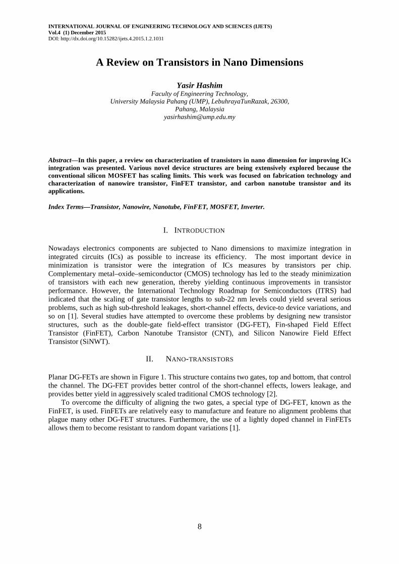
II. NANO-TRANSISTORS Planar DG-FETs are shown in Figure 1. This structure contains two gates, top and bottom, that control the channel. The DG-FET provides better control of the short-channel effects, lowers leakage, and provides better yield in aggressively scaled traditional CMOS technology [2]. To overcome the difficulty of aligning the two gates, a special type of DG-FET, known as the FinFET, is used. FinFETs are relatively easy to manufacture and feature no alignment problems that plague many other DG-FET structures. Furthermore, the use of a lightly doped channel in FinFETs allows them to become resistant to random dopant variations [1].
INTERNATIONAL JOURNAL OF ENGINEERING TECHNOLOGY AND SCIENCES (IJETS) Vol.4 (1) December 2015 DOI: http://dx.doi.org/10.15282/ijets.4.2015.1.2.1031
9
Figure 1 DG-FET structure [1]
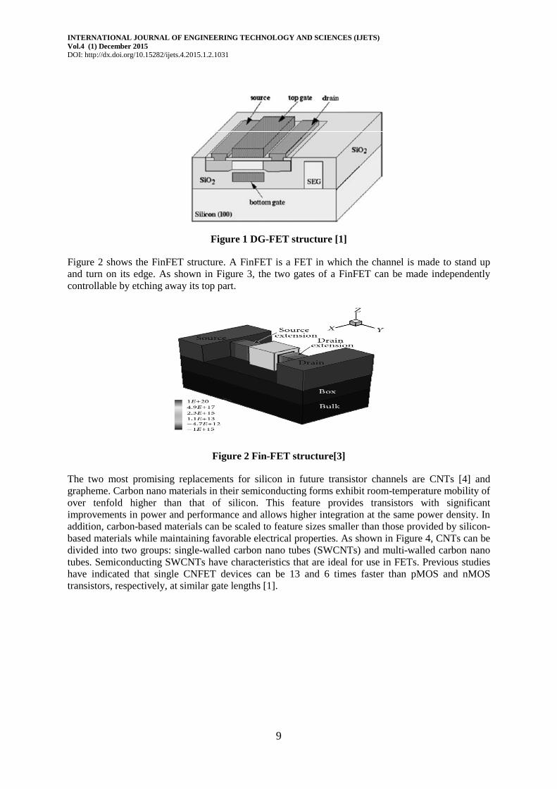
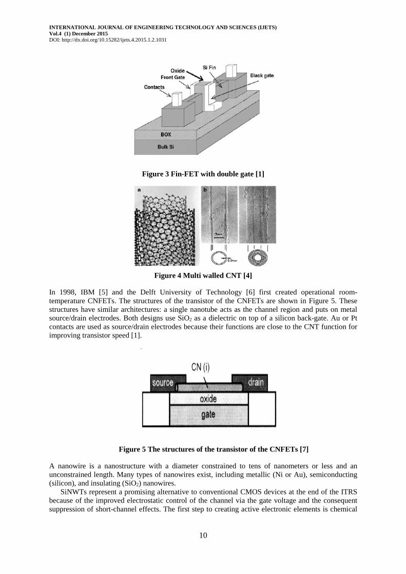
Figure 2 shows the FinFET structure. A FinFET is a FET in which the channel is made to stand up and turn on its edge. As shown in Figure 3, the two gates of a FinFET can be made independently controllable by etching away its top part.
Figure 2 Fin-FET structure[3]
The two most promising replacements for silicon in future transistor channels are CNTs [4] and grapheme. Carbon nano materials in their semiconducting forms exhibit room-temperature mobility of over tenfold higher than that of silicon. This feature provides transistors with significant improvements in power and performance and allows higher integration at the same power density. In addition, carbon-based materials can be scaled to feature sizes smaller than those provided by silicon-based materials while maintaining favorable electrical properties. As shown in Figure 4, CNTs can be divided into two groups: single-walled carbon nano tubes (SWCNTs) and multi-walled carbon nano tubes. Semiconducting SWCNTs have characteristics that are ideal for use in FETs. Previous studies have indicated that single CNFET devices can be 13 and 6 times faster than pMOS and nMOS transistors, respectively, at similar gate lengths [1].
INTERNATIONAL JOURNAL OF ENGINEERING TECHNOLOGY AND SCIENCES (IJETS) Vol.4 (1) December 2015 DOI: http://dx.doi.org/10.15282/ijets.4.2015.1.2.1031
10
Figure 3 Fin-FET with double gate [1]
Figure 4 Multi walled CNT [4]
In 1998, IBM [5] and the Delft University of Technology [6] first created operational room-temperature CNFETs. The structures of the transistor of the CNFETs are shown in Figure 5. These structures have similar architectures: a single nanotube acts as the channel region and puts on metal source/drain electrodes. Both designs use SiO2 as a dielectric on top of a silicon back-gate. Au or Pt contacts are used as source/drain electrodes because their functions are close to the CNT function for improving transistor speed [1].
Figure 5 The structures of the transistor of the CNFETs [7]
A nanowire is a nanostructure with a diameter constrained to tens of nanometers or less and an unconstrained length. Many types of nanowires exist, including metallic (Ni or Au), semiconducting (silicon), and insulating (SiO2) nanowires. SiNWTs represent a promising alternative to conventional CMOS devices at the end of the ITRS because of the improved electrostatic control of the channel via the gate voltage and the consequent suppression of short-channel effects. The first step to creating active electronic elements is chemical
INTERNATIONAL JOURNAL OF ENGINEERING TECHNOLOGY AND SCIENCES (IJETS) Vol.4 (1) December 2015 DOI: http://dx.doi.org/10.15282/ijets.4.2015.1.2.1031
11
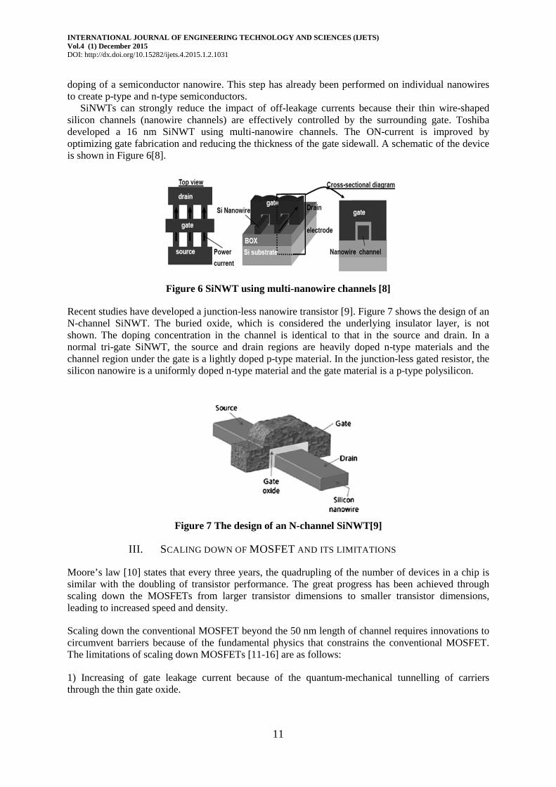
doping of a semiconductor nanowire. This step has already been performed on individual nanowires to create p-type and n-type semiconductors. SiNWTs can strongly reduce the impact of off-leakage currents because their thin wire-shaped silicon channels (nanowire channels) are effectively controlled by the surrounding gate. Toshiba developed a 16 nm SiNWT using multi-nanowire channels. The ON-current is improved by optimizing gate fabrication and reducing the thickness of the gate sidewall. A schematic of the device is shown in Figure 6[8].
Figure 6 SiNWT using multi-nanowire channels [8]
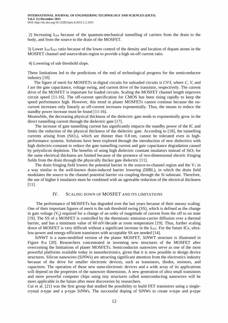
Recent studies have developed a junction-less nanowire transistor [9]. Figure 7 shows the design of an N-channel SiNWT. The buried oxide, which is considered the underlying insulator layer, is not shown. The doping concentration in the channel is identical to that in the source and drain. In a normal tri-gate SiNWT, the source and drain regions are heavily doped n-type materials and the channel region under the gate is a lightly doped p-type material. In the junction-less gated resistor, the silicon nanowire is a uniformly doped n-type material and the gate material is a p-type polysilicon.
Figure 7 The design of an N-channel SiNWT[9]
III. SCALING DOWN OF MOSFET AND ITS LIMITATIONS Moore’s law [10] states that every three years, the quadrupling of the number of devices in a chip is similar with the doubling of transistor performance. The great progress has been achieved through scaling down the MOSFETs from larger transistor dimensions to smaller transistor dimensions, leading to increased speed and density.
Scaling down the conventional MOSFET beyond the 50 nm length of channel requires innovations to circumvent barriers because of the fundamental physics that constrains the conventional MOSFET. The limitations of scaling down MOSFETs [11-16] are as follows:
1) Increasing of gate leakage current because of the quantum-mechanical tunnelling of carriers through the thin gate oxide.
INTERNATIONAL JOURNAL OF ENGINEERING TECHNOLOGY AND SCIENCES (IJETS) Vol.4 (1) December 2015 DOI: http://dx.doi.org/10.15282/ijets.4.2015.1.2.1031
12
2) Increasing IOFF because of the quantum-mechanical tunnelling of carriers from the drain to the body, and from the source to the drain of the MOSFET.
3) Lower ION/IOFF ratio because of the lower control of the density and location of dopant atoms in the MOSFET channel and source/drain region to provide a high on-off current ratio.
4) Lowering of sub threshold slope.
These limitations led to the predictions of the end of technological progress for the semiconductor industry [10]. The figure of merit for MOSFETs in digital circuits for unloaded circuits is CV/I, where C, V, and I are the gate capacitance, voltage swing, and current drive of the transistor, respectively. The current drive of the MOSFET is important for loaded circuits. Scaling the MOSFET channel length improves circuit speed [11-16]. The off-current specification for CMOS has been rising rapidly to keep the speed performance high. However, this trend in planer MOSFETs cannot continue because the on-current increases only linearly as off-current increases exponentially. Thus, the means to reduce the standby power increase must be found [11-16]. Meanwhile, the decreasing physical thickness of the dielectric gate tends to exponentially grow in the direct tunnelling current through the dielectric gate [17]. The increase of gate tunnelling current has significantly impacts the standby power of the IC and limits the reduction of the physical thickness of the dielectric gate. According to [18], the tunnelling currents arising from (SiO2), which are thinner than 0.8 nm, cannot be tolerated even in high-performance systems. Solutions have been explored through the introduction of new dielectrics with high dielectric-constant to reduce the gate tunnelling current and gate capacitance degradation caused by polysilicon depletion. The benefits of using high dielectric constant insulators instead of SiO2 for the same electrical thickness are limited because of the presence of two-dimensional electric fringing fields from the drain through the physically thicker gate dielectric [11]. The drain fringing field lowers the potential barrier in the source-to-channel region and the VT in a way similar to the well-known drain-induced barrier lowering (DIBL), in which the drain field modulates the source to the channel potential barrier via coupling through the Si substrate. Therefore, the use of higher k insulators must be combined with an agreeable reduction of the electrical thickness [11].
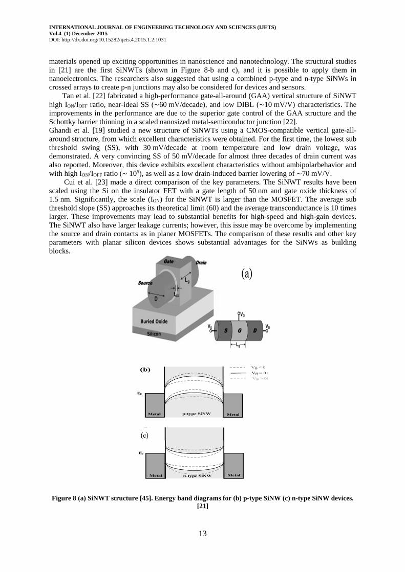
IV. SCALING DOWN OF MOSFET AND ITS LIMITATIONS The performance of MOSFETs has degraded over the last years because of their uneasy scaling. One of their important figures of merit is the sub threshold swing (SS), which is defined as the change in gate voltage (Vg) required for a change of an order of magnitude of current from the off to on state [19]. The SS of a MOSFET is controlled by the thermionic emission-carrier diffusion over a thermal barrier, and has a minimum value of 60 mV/decade at room temperature [19]. Thus, further scaling down of MOSFET is very difficult without a significant increase in the IOFF. For the future ICs, ultra-low-power and energy-efficient transistors with acceptable SS are needed [14]. SiNWT is a nano-modified version of the planer MOSFET, SiNWT structure is illustrated in Figure 8-a [20]. Researchers concentrated in inventing new structures of the MOSFET after overcoming the limitations of planer MOSFETs. Semiconductor nanowires serve as one of the most powerful platforms available today in nanoelectronics, given that it is now possible to design device structures. Silicon nanowires (SiNWs) are attracting significant attention from the electronics industry because of the drive for smaller electronic devices, such as transistors, diodes, resistors, and capacitors. The operation of these new nano-electronic devices and a wide array of its applications will depend on the properties of the nanowire dimensions. A new generation of ultra small transistors and more powerful computer chips using tiny structures called semiconducting nanowires will be more applicable in the future after more discoveries by researchers. Cui et al. [21] was the first group that studied the possibility to build FET transistors using a single-crystal n-type and a p-type SiNWs. The successful doping of SiNWs to create n-type and p-type
INTERNATIONAL JOURNAL OF ENGINEERING TECHNOLOGY AND SCIENCES (IJETS) Vol.4 (1) December 2015 DOI: http://dx.doi.org/10.15282/ijets.4.2015.1.2.1031
13
materials opened up exciting opportunities in nanoscience and nanotechnology. The structural studies in [21] are the first SiNWTs (shown in Figure 8-b and c), and it is possible to apply them in nanoelectronics. The researchers also suggested that using a combined p-type and n-type SiNWs in crossed arrays to create p-n junctions may also be considered for devices and sensors. Tan et al. [22] fabricated a high-performance gate-all-around (GAA) vertical structure of SiNWT high ION/IOFF ratio, near-ideal SS (∼60 mV/decade), and low DIBL (∼10 mV/V) characteristics. The improvements in the performance are due to the superior gate control of the GAA structure and the Schottky barrier thinning in a scaled nanosized metal-semiconductor junction [22]. Ghandi et al. [19] studied a new structure of SiNWTs using a CMOS-compatible vertical gate-all-around structure, from which excellent characteristics were obtained. For the first time, the lowest sub threshold swing (SS), with 30 mV/decade at room temperature and low drain voltage, was demonstrated. A very convincing SS of 50 mV/decade for almost three decades of drain current was also reported. Moreover, this device exhibits excellent characteristics without ambipolarbehavior and with high ION/IOFF ratio (∼ 105), as well as a low drain-induced barrier lowering of ∼70 mV/V. Cui et al. [23] made a direct comparison of the key parameters. The SiNWT results have been scaled using the Si on the insulator FET with a gate length of 50 nm and gate oxide thickness of 1.5 nm. Significantly, the scale (ION) for the SiNWT is larger than the MOSFET. The average sub threshold slope (SS) approaches its theoretical limit (60) and the average transconductance is 10 times larger. These improvements may lead to substantial benefits for high-speed and high-gain devices. The SiNWT also have larger leakage currents; however, this issue may be overcome by implementing the source and drain contacts as in planer MOSFETs. The comparison of these results and other key parameters with planar silicon devices shows substantial advantages for the SiNWs as building blocks.
Figure 8 (a) SiNWT structure [45]. Energy band diagrams for (b) p-type SiNW (c) n-type SiNW devices. [21]
INTERNATIONAL JOURNAL OF ENGINEERING TECHNOLOGY AND SCIENCES (IJETS) Vol.4 (1) December 2015 DOI: http://dx.doi.org/10.15282/ijets.4.2015.1.2.1031
14
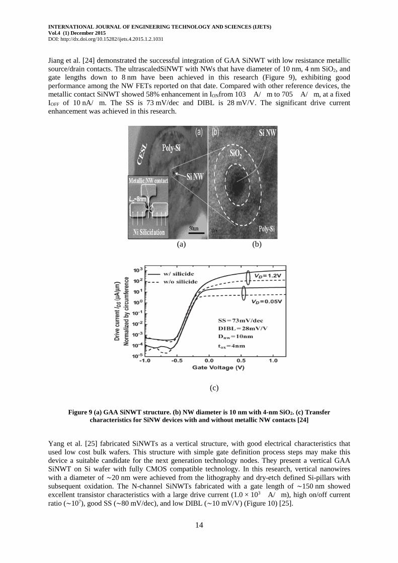
Jiang et al. [24] demonstrated the successful integration of GAA SiNWT with low resistance metallic source/drain contacts. The ultrascaledSiNWT with NWs that have diameter of 10 nm, 4 nm SiO2, and gate lengths down to 8 nm have been achieved in this research (Figure 9), exhibiting good performance among the NW FETs reported on that date. Compared with other reference devices, the metallic contact SiNWT showed 58% enhancement in IONfrom 103 �A/�m to 705 �A/�m, at a fixed IOFF of 10 nA/�m. The SS is 73 mV/dec and DIBL is 28 mV/V. The significant drive current enhancement was achieved in this research.
Figure 9 (a) GAA SiNWT structure. (b) NW diameter is 10 nm with 4-nm SiO2. (c) Transfer characteristics for SiNW devices with and without metallic NW contacts [24]
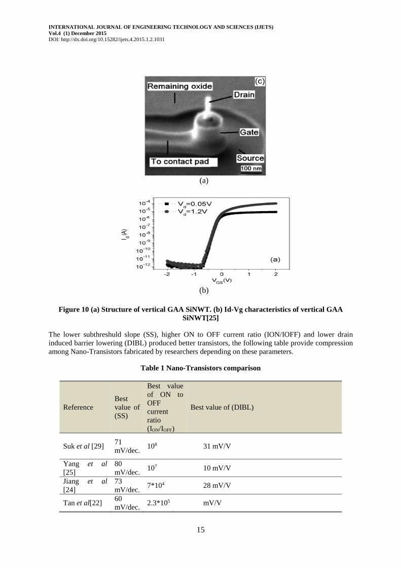
Yang et al. [25] fabricated SiNWTs as a vertical structure, with good electrical characteristics that used low cost bulk wafers. This structure with simple gate definition process steps may make this device a suitable candidate for the next generation technology nodes. They present a vertical GAA SiNWT on Si wafer with fully CMOS compatible technology. In this research, vertical nanowires with a diameter of ∼20 nm were achieved from the lithography and dry-etch defined Si-pillars with subsequent oxidation. The N-channel SiNWTs fabricated with a gate length of ∼150 nm showed excellent transistor characteristics with a large drive current (1.0 × 10³ �A/�m), high on/off current ratio (∼107), good SS (∼80 mV/dec), and low DIBL (∼10 mV/V) (Figure 10) [25].
(a) (b)
(c)
INTERNATIONAL JOURNAL OF ENGINEERING TECHNOLOGY AND SCIENCES (IJETS) Vol.4 (1) December 2015 DOI: http://dx.doi.org/10.15282/ijets.4.2015.1.2.1031
15
Figure 10 (a) Structure of vertical GAA SiNWT. (b) Id-Vg characteristics of vertical GAA SiNWT[25]
The lower subthreshuld slope (SS), higher ON to OFF current ratio (ION/IOFF) and lower drain induced barrier lowering (DIBL) produced better transistors, the following table provide compression among Nano-Transistors fabricated by researchers depending on these parameters.
Table 1 Nano-Transistors comparison
Reference Best value of (SS)
Best value of ON to OFF current ratio (ION/IOFF)
Best value of (DIBL)
Suk et al [29] 71 mV/dec.
108 31 mV/V
Yang et al [25]
80 mV/dec.
107 10 mV/V
Jiang et al [24]
73 mV/dec.
7*104 28 mV/V
Tan et al[22] 60 mV/dec.
2.3*105 mV/V
(a)
(b)
INTERNATIONAL JOURNAL OF ENGINEERING TECHNOLOGY AND SCIENCES (IJETS) Vol.4 (1) December 2015 DOI: http://dx.doi.org/10.15282/ijets.4.2015.1.2.1031
16
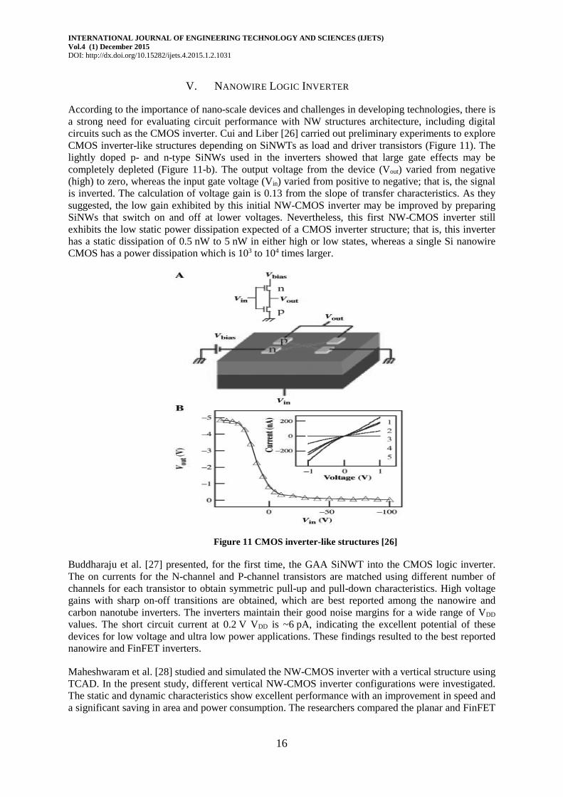
V. NANOWIRE LOGIC INVERTER According to the importance of nano-scale devices and challenges in developing technologies, there is a strong need for evaluating circuit performance with NW structures architecture, including digital circuits such as the CMOS inverter. Cui and Liber [26] carried out preliminary experiments to explore CMOS inverter-like structures depending on SiNWTs as load and driver transistors (Figure 11). The lightly doped p- and n-type SiNWs used in the inverters showed that large gate effects may be completely depleted (Figure 11-b). The output voltage from the device (Vout) varied from negative (high) to zero, whereas the input gate voltage (Vin) varied from positive to negative; that is, the signal is inverted. The calculation of voltage gain is 0.13 from the slope of transfer characteristics. As they suggested, the low gain exhibited by this initial NW-CMOS inverter may be improved by preparing SiNWs that switch on and off at lower voltages. Nevertheless, this first NW-CMOS inverter still exhibits the low static power dissipation expected of a CMOS inverter structure; that is, this inverter has a static dissipation of 0.5 nW to 5 nW in either high or low states, whereas a single Si nanowire CMOS has a power dissipation which is 103 to 104 times larger.
Figure 11 CMOS inverter-like structures [26]
Buddharaju et al. [27] presented, for the first time, the GAA SiNWT into the CMOS logic inverter. The on currents for the N-channel and P-channel transistors are matched using different number of channels for each transistor to obtain symmetric pull-up and pull-down characteristics. High voltage gains with sharp on-off transitions are obtained, which are best reported among the nanowire and carbon nanotube inverters. The inverters maintain their good noise margins for a wide range of VDD values. The short circuit current at 0.2 V VDD is ~6 pA, indicating the excellent potential of these devices for low voltage and ultra low power applications. These findings resulted to the best reported nanowire and FinFET inverters.
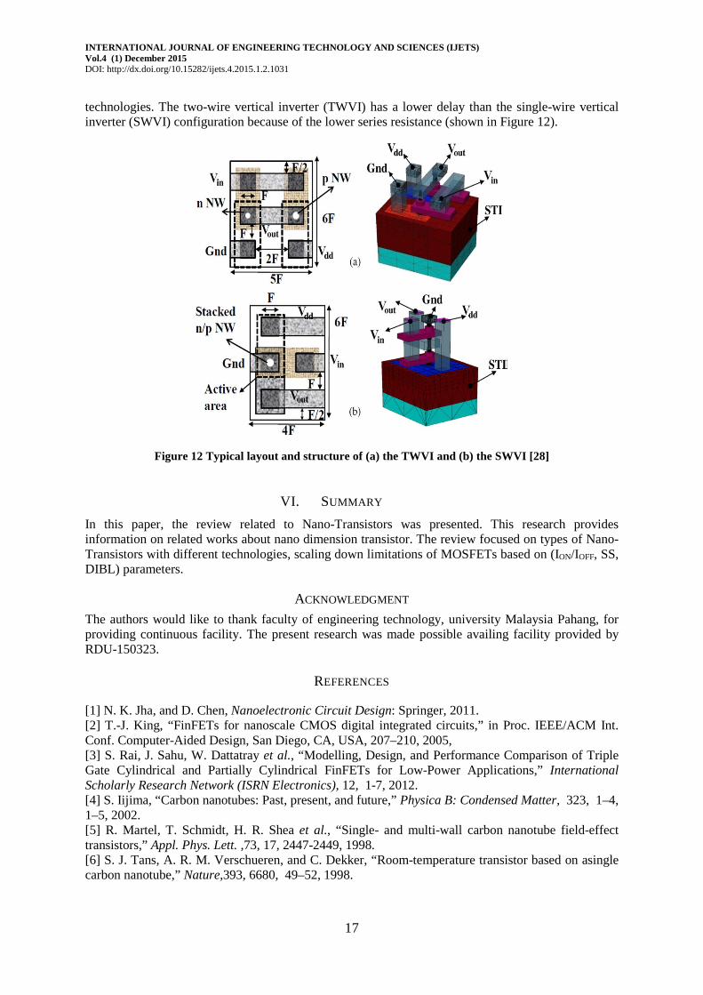
Maheshwaram et al. [28] studied and simulated the NW-CMOS inverter with a vertical structure using TCAD. In the present study, different vertical NW-CMOS inverter configurations were investigated. The static and dynamic characteristics show excellent performance with an improvement in speed and a significant saving in area and power consumption. The researchers compared the planar and FinFET
INTERNATIONAL JOURNAL OF ENGINEERING TECHNOLOGY AND SCIENCES (IJETS) Vol.4 (1) December 2015 DOI: http://dx.doi.org/10.15282/ijets.4.2015.1.2.1031
17
technologies. The two-wire vertical inverter (TWVI) has a lower delay than the single-wire vertical inverter (SWVI) configuration because of the lower series resistance (shown in Figure 12).
Figure 12 Typical layout and structure of (a) the TWVI and (b) the SWVI [28]
VI. SUMMARY
In this paper, the review related to Nano-Transistors was presented. This research provides information on related works about nano dimension transistor. The review focused on types of Nano-Transistors with different technologies, scaling down limitations of MOSFETs based on (ION/IOFF, SS, DIBL) parameters.
ACKNOWLEDGMENT
The authors would like to thank faculty of engineering technology, university Malaysia Pahang, for providing continuous facility. The present research was made possible availing facility provided by RDU-150323.
REFERENCES [1] N. K. Jha, and D. Chen, Nanoelectronic Circuit Design: Springer, 2011. [2] T.-J. King, “FinFETs for nanoscale CMOS digital integrated circuits,” in Proc. IEEE/ACM Int. Conf. Computer-Aided Design, San Diego, CA, USA, 207–210, 2005, [3] S. Rai, J. Sahu, W. Dattatray et al., “Modelling, Design, and Performance Comparison of Triple Gate Cylindrical and Partially Cylindrical FinFETs for Low-Power Applications,” International Scholarly Research Network (ISRN Electronics), 12, 1-7, 2012. [4] S. Iijima, “Carbon nanotubes: Past, present, and future,” Physica B: Condensed Matter, 323, 1–4, 1–5, 2002. [5] R. Martel, T. Schmidt, H. R. Shea et al., “Single- and multi-wall carbon nanotube field-effect transistors,” Appl. Phys. Lett. ,73, 17, 2447-2449, 1998. [6] S. J. Tans, A. R. M. Verschueren, and C. Dekker, “Room-temperature transistor based on asingle carbon nanotube,” Nature,393, 6680, 49–52, 1998.
INTERNATIONAL JOURNAL OF ENGINEERING TECHNOLOGY AND SCIENCES (IJETS) Vol.4 (1) December 2015 DOI: http://dx.doi.org/10.15282/ijets.4.2015.1.2.1031
18
[7] J. Appenzeller, Y.-M. Lin, J. Knoch et al., “Comparing Carbon Nanotube Transistors—The Ideal Choice: A Novel Tunneling Device Design,” IEEE TRANSACTIONS ON ELECTRON DEVICES, 52, 12, 2568-2576, 2005. [8] T. Corporation. "Toshiba develops silicon nanowire transistor for 16-nm generation and beyond," http://www.physorg.com/news195834466.html. [9] J. P. Colinge, C. W. Lee, A. Afzalian et al., “Nanowire transistors without junctions,” Nature Nanotech., vol. 5, 3225-229, 2010. [10] P. Packan, “Pushing the Limits,” Science,. 285,. 5436, 2079-2081, 1999. [11] H.-S. P. Wong, “Beyond the conventional transistor,” IBM J. RES. & DEV, vol. 46, no. 2/3, MARCH/MAY, 2002. [12] M. Luisier, A. Schenk, and W. Fichtner, “Three-dimensional Modeling of Gate Leakage in Si Nanowire Transistors,” in IEEE International Electron Devices Meeting (IEDM) ,. 733-6. 2007 [13] P. F. Butzen, and R. P. Ribas, "LEAKAGE CURRENT IN SUB-MICROMETER CMOS GATES," Book chapter (Advanced Topics on VLSI Design). [14] Y.-C. Yeo, T.-J. King, and C. Hu, “MOSFET Gate Leakage Modeling and Selection Guide for Alternative Gate Dielectrics Based on Leakage Considerations,” IEEE TRANSACTIONS ON ELECTRON DEVICES,. 50,. 41027-35, 2003. [15] S. G. Narendra, and A. P. Chandrakasan, Leakage in nanometer CMOS technologies: Springer, 2006. [16] F. Assad, Z. Ren, D. Vasileska et al., “On the Performance Limits for Si MOSFET’s: A Theoretical Study,” IEEE TRANSACTIONS ON ELECTRON DEVICES,. 47, 1,. 232-40, 2000. [17] S. H. Lo, D. Buchanan, Y. Taur et al., “Quantum-Mechanical Modeling of Electron Tunneling Current from the Inversion Layer of Ultra-Thin-Oxide nMOSFETs,” IEEE Electron Device Lett.,.18, 209–211, 1997. [18] D. Frank, R. Dennard, E. Nowak et al., “Device Scaling Limits of Si MOSFETs and Their Application Dependencies,” Proc. IEEE, 89, 259 –288, 2001. [19] R. Gandhi, Z. Chen, N. Singh et al., “Vertical Si-Nanowire n-Type Tunneling FETs With Low Sub threshold Swing (≤ 50 mV/decade) at Room Temperature,” IEEE ELECTRON DEVICE LETTERS, 32,. 4,. 437-9, 2011. [20] Y. B. Liaoa, M.-H. Chiangb, K. Kimc et al., “Assessment of structure variation in silicon nanowire FETs and impact on SRAM,” Microelectronics Journal, 43,. 5, 300–304, 2012. [21] Y. Cui, X. Duan, J. Hu et al., “Doping and Electrical Transport in Silicon Nanowires,” J. Phys. Chem. B, vol. 104, 22, 5213-16, 2000. [22] E. J. Tan, K. L. Pey, N. Singh et al., “Nickel Silicided Schottky Junction CMOS Transistors With Gate-All-Around Nanowire Channels,” IEEE ELECTRON DEVICE LETTERS, 29, 8, 902-5, 2008. [23] Y. Cui, Z. Zhong, D. Wang et al., “High Performance Silicon Nanowire Field Effect Transistors,” Nano Lett.,. 3. 2, 149-152, 2003. [24] Y. Jiang, T. Y. Liow, N. Singh et al., “Nickel Salicided Source/Drain Extensions for Performance Improvement in Ultrascaled (Sub 10 nm) Si-Nanowire Transistors,” IEEE ELECTRON DEVICE LETTERS, vol. 30, no. 2, pp. 195-7, 2009. [25] B. Yang, K. D. Buddharaju, S. H. G. Teo et al., “Vertical Silicon-Nanowire Formation and Gate-All-Around MOSFET,” IEEE ELECTRON DEVICE LETTERS,. 29, 7, 791-4, 2008. [26] Y. Cui, and C. M. Lieber, “Functional Nanoscale Electronic Devices Assembled Using Silicon Nanowire Building Blocks,” SCIENCE, vol. 291, pp. 851-3, 2001. [27] K. D. Buddharaju, N. Singh, S. C. Rustagi et al., “Gate-all-around Si-nanowire CMOS inverter logic fabricated using top-down approach,” in European Solid-State Device Research Conference (ESSDERC 2007), 2007, 303-306. [28] S. Maheshwaram, S. K. Manhas, G. Kaushal et al., “Vertical Silicon Nanowire Gate-All-Around Field Effect Transistor Based Nanoscale CMOS,” IEEE ELECTRON DEVICE LETTERS, 32,. 8, 1011-3, 2011. [29] Sung Dae Suk, Sung-Young Lee, Sung-Min Kim et al., "High performance 5nm radius Twin Silicon Nanowire MOSFET (TSNWFET) : fabrication on bulk si wafer, characteristics, and reliability." 717 - 720. 2012


![[Chapter III] Basic Knowledge of Discrete Semiconductor ......transistors (IGBTs) Power transistors (2SAxx,2SBxx,2SCxx,2SDxx, TTAxx,TTBxx,TTCxx,TTDxx) Types of Transistors Transistors](https://img.pdfslide.us/doc/110x75/5e766014341a1a707d5f4c34/chapter-iii-basic-knowledge-of-discrete-semiconductor-transistors-igbts.jpg)