Embed Size (px)
Citation preview

R
As
Ma
b
c
Jd
a
ARRAA
KSSPSNA
0d
Analytica Chimica Acta 693 (2011) 7–25
Contents lists available at ScienceDirect
Analytica Chimica Acta
journa l homepage: www.e lsev ier .com/ locate /aca
eview
review on the fabrication of substrates for surface enhanced Ramanpectroscopy and their applications in analytical chemistry
eikun Fana,b,1, Gustavo F.S. Andradec,1, Alexandre G. Brolod,∗
Department of Mechanical and Material Engineering, University of Western Ontario, London, ON, CanadaGreen Energy and Green Technology R&D Center, Chengdu Institute of Chemical Materials, Chengdu, ChinaInstituto de Ciências Exatas, Departamento de Química, Universidade Federal de Juiz de Fora, Campus Universitário s/n, CEP 36036-900,
uiz de Fora, BrazilDepartment of Chemistry, University of Victoria, PO Box 3055, Victoria, BC V8W 3V6, Canada
r t i c l e i n f o
rticle history:eceived 10 December 2010eceived in revised form 24 February 2011ccepted 1 March 2011vailable online 6 March 2011
a b s t r a c t
This work reviews different types of substrates used for surface-enhanced Raman scattering (SERS) thathave been developed in the last 10 years. The different techniques of self-assembly to immobilize metallicnanoparticles on solid support are covered. An overview of SERS platforms developed using nanolithog-raphy methods, including electron-beam (e-beam) lithography and focused ion beam (FIB) milling arealso included, together with several examples of template-based methodologies to generate metallic
eywords:urface-enhanced Raman scatteringERSlasmonicsensorsanolithographynalytical spectroscopy
nano-patterns. The potential of SERS to impact several aspects of analytical chemistry is demonstratedby selected examples of applications in electrochemistry, biosensing, environmental analysis, and remotesensing. This review shows that highly enhancing SERS substrates with a high degree of reliability andreproducibility can now be fabricated at relative low cost, indicating that SERS may finally realize its fullpotential as a very sensitive tool for routine analytical applications.
© 2011 Elsevier B.V. All rights reserved.
interests are on surfaceenhanced Raman scattering(SERS) and its applications in electrochemistry andbiosensing.
Meikun Fan was born in 1976. He obtained hisBachelor’s (1999) and Master’s degree (2002) fromSouthwest China Normal University. He then workedas a university lecturer in Dalian University of Tech-nology for three years. In 2005 he moved to theUniversity of Victoria (Canada) and worked with Pro-fessor Alexandre G. Brolo for his PhD degree (2010).He is now a Postdoctoral Fellow at the Univer-sity of Western Ontario. His research interests aremainly centered on surface-enhanced Raman scatter-ing (SERS) and opto-microfluidics.
∗ Corresponding author. Tel.: +1 250 721 7167.E-mail address: [email protected] (A.G. Brolo).
1 These authors contributed the same.
003-2670/$ – see front matter © 2011 Elsevier B.V. All rights reserved.oi:10.1016/j.aca.2011.03.002
Gustavo F.S. Andrade obtained his Bachelor, Master,and Doctoral degrees from the Instituto de Quim-ica of the University of Sao Paulo in Brazil. In2008–2009 he was awarded a postdoctoral fellowshipfrom the Canadian Bureau for International Educa-tion – Department of Foreign Affairs and InternationalTrade (CBIE-DFAIT) and to the University of Victoria(Canada) to work with Dr. Alexandre Brolo. He is nowan assistant professor at the Department of Chemistryof the University of Juiz de Fora in Brazil. His research
8 himic
1
epmottmpo
eiqnoftlwwthtb
1
fii1sud
Rtmoartotte
M. Fan et al. / Analytica C
Alexandre G. Brolo is an associate professor at theUniversity of Victoria in British Columbia, Canada. Heobtained his M.Sc. from the University of Sao Paulo(Brazil) in 1989 and his Ph.D. from the Universityof Waterloo (Canada). Dr. Brolo’s research interestare of the fabrication of nanostructured metal sur-faces; the investigation of their optical properties;and their application in analytical chemistry. He iswellknown for his work on the development of newtypes of surface Plasmon resonance sensors and on thefield of surface-enhanced spectroscopy, particularlyon surface-enhanced Raman scattering (SERS).
. Introduction and outlook
Surface-enhanced Raman scattering (SERS) consists on thenhancement of the Raman scattering intensity by molecules in theresence of a nanostructured metallic surface. The SERS enhance-ent factor (ratio between the Raman signals from a given number
f molecules in the presence and in the absence of the nanostruc-ure) depends strongly on the size and shape of the nanostructureshat give rise to the effect. An average value for the SERS enhance-
ent is around 106, but the localized enhancement may reacheaks of 1010 at certain highly efficient sub-wavelength regionsf the surface [1].
SERS has grown to become a very active field of research in sev-ral areas of materials and analytical sciences [2]. The effervescencen SERS research motivated the recent publication of two high-uality monographs by Aroca [3] and Le Ru and Etchegoin [4] thaticely cover the principles of SERS and its applications, and a seriesf recent review articles that cover several aspects of the effect,rom basic concepts to specific applications [5–9]. In this review,he recent development on SERS substrates (which are the metal-ic nanostructured platforms that support the effect) is discussed,
ith focus on their analytical applications. The discussion will startith a brief historical survey of SERS, followed by an overview on
he different types of substrates developed for SERS. The SERS fieldas a great breath, and this review cannot be exhaustive; hence,he scope of the nanostructures that are covered in this work wille delineated in Section 1.3.
.1. Historical development of SERS
The detection of adsorbed monolayers on metallic sur-aces by ordinary Raman spectroscopy is a very challeng-ng problem because of the very small cross-section of thenelastic scattering event, typically in the order or 10−28 to0−30 cm2 molecule−1 stereoradian−1 [10]. With such a low cross-ection, the scattering from about 1012 to 1014 molecules cm−2,sually present in a monolayer, is hardly going to be enough to beetected even by the most efficient modern Raman spectrometer.
The detection of monolayers adsorbed on metallic surfaces byaman scattering is particularly important in the context of spec-roelectrochemistry. The focus in that area is to use spectroscopic
ethods to probe electrochemical processes in real time, and mostf the relevant electrochemical systems involve metallic electrodesnd aqueous solutions. Water yields a lower background in Raman,elative to IR absorption, and the use of visible radiation for excita-
ion and detection are also important advantages for the applicationf Raman to study electrochemical systems. Based on those advan-ages, a few spectroelectrochemists were trying very hard duringhe 1970s to obtain the Raman signature from adsorbed monolay-rs from metal surfaces under electrochemical control, but withouta Acta 693 (2011) 7–25
too much success. A notable exception was the detection of Hg2Br2,Hg2Cl2 and HgO in Hg electrode [11], made possible by the unusu-ally high cross-section of mercury ion species. It should also bementioned the characterization of highly absorbing ion radical gen-erated by the reduction of tetracyanoquinodimethane (TCNQ), dueto the strong resonance Raman scattering presented by the reducedspecie TCNQ·− [12]. In this scenario, Fleischmann et al. decided totry to increase the number of adsorbed molecules by using a rough-ened metal electrode surface. They reported, in 1974 [13], veryhigh signal-to-noise ratio Raman spectra of pyridine adsorbed onelectrochemically roughened Ag electrodes. The authors attributedthe enhancement in the Raman intensity to an increase in thearea of the Ag electrode by the electrochemical roughening. Twoyears later, two groups independently [14,15] showed that theRaman scattering oversized by far the intensity expected from thearea increase generated by the roughening procedure. The calcu-lated intensity enhancement was around 105–106. The conceptof enhanced optical effects in metallic surfaces was subsequentlyestablished by Moskovits [16]. This new phenomenon catalyzed asignificant amount of efforts by a large number of research groups,leading to a fast increase in the understanding of the effect, whichwas named surface-enhanced Raman scattering (SERS).
It became clear very early that roughened Ag electrodes werenot the only type of platforms that could be used as SERS sub-strates. The use of Au and Cu nanoparticles (NPs) was verified inthe very first years after the discovery of SERS [17]. The abilityto support the excitation of surface-plasmons (SPs) in the visibleregion is a characteristic shared by Ag, Au and Cu, and a great partof the enhancement in SERS was early attributed to those reso-nances [16,18]. The excitation of SPs causes an enhancement in theelectric-field localized around the nano-sized metallic structures,leading to both the excitation light and the scattered radiationto be surface-enhanced. The local-field can be enhanced by a fargreater extent when neighboring nano-features interact with eachother over distances in the order of 1–2 nm [19]. The regions ofhighly enhanced local electromagnetic field are called “SERS hot-spots”. The SPs-based model for SERS successfully explains most ofthe experimental results, but not all of them. This model does nottake into account the dependence of the SERS enhancement on thechemical structure of the probe molecule. This dependence wasdealt with by the so-called chemical models for SERS. The mostcommon of the chemical models assume the appearance of newelectronic states due to chemisorption, and the chemical dependentfeatures of SERS are taken into account using a theoretical frame-work strongly related to the resonance Raman effect [20–22]. Thetheoretical efforts in the early 1980s established the SP-based andthe chemical mechanisms as the main contributions to the SERSeffect [23].
In the mid-1980s, the focus on SERS research started to movefrom the fundamental understanding of the phenomenon to theexploration of promising analytical applications of SERS [24–26].The initial studies have shown that the main difficulty with SERSwas that even small variations in the substrate preparation, whichusually could not be well controlled, resulted in significant changesin the SERS performance. This drawback prevented for several yearsthe expansion of SERS as a quantitative tool, although the applica-tion of SERS for qualitative trace detection was being developed inseveral directions, spanning from biosensors [27] to electrochemi-cal studies [28,29].
The next major milestone in the development of the SERS fieldwas the observation in 1997 of SERS spectra from single molecules
(SM-SERS) by two groups independently [30,31]. The detectionof single molecules elevated SERS to the very restrict group oftechniques able to attain this ultimate limit of detection, togetherwith, for instance, fluorescence spectroscopy and scanning tunnel-ing methods. A great characteristic of SERS that makes it unique
himic
rtotttfys
1
eutnmtsAttm
essn
slbomasUsah
pTMhSaln
MtISaosPc
ittpt
M. Fan et al. / Analytica C
elative to other single-molecule methods is that the Raman scat-ered signal contains the vibrational information from the analytef interest, which allows a much higher specificity when comparedo, for instance, fluorescence spectroscopy. Single molecule detec-ion gave a new direction to the SERS research field. This fact, alliedo the great advances in nanofabrication and synthetic techniquesor the preparation of metallic nanoparticles (MNPs) in the last 15ears [32], resulted in a significant increase in the reports of newubstrates for SERS [33,34].
.2. SERS substrates: An overview
The original substrates for SERS were electrochemically rough-ned metal electrodes [13]. Metallic nanoparticles (MNPs) weresed shortly after the discovery of the SERS effect and becamehe most studied class of substrates. The research emphasis onanostructures for SERS is justified by the wide possibilities of opti-ization parameters, since both the frequency and magnitude of
he maximum field enhancement are strongly dependent on thehape, size and arrangement of the metallic nanofeatures [35].lthough the possibility of tuning the size and shape of nanostruc-
ures has quickly grown in the last 15 years, there are argumentshat they are still at rudimentary stage, and much greater develop-
ents are to be expected in the years to come [32].The SERS substrates can be arbitrarily classified in three cat-
gories: (1) MNPs in suspension; (2) MNPs immobilized on solidubstrates; (3) Nanostructures fabricated directly on solid sub-trates, which includes nanolithography and template synthesis ofanostructures.
The synthesis strategy for the nanostructures shapes and sizespan a wide range of procedures, as might be attested from recentiterature reviews [32,36,37]. The synthesis of spheroid MNPs haseen exhaustively studied, and several well established meth-ds are available [38,39]. The wet synthesis of anisotropic MNPsay be achieved by selective adsorption of protective layers such
s cetyltrimethylammonium bromide (CTAB), and several otherelective adsorbates [32], that directs the growth process [40].V–visible light driven metal-ion reduction [41], and template
ynthesis [2,42–45] have also been used. The universe of possiblenisotropic structures is very wide and the control over the processas shown great improvements.
The simplest SERS experiments are realized with MNPs in sus-ension in the presence of a certain concentration of the analyte.he main drawback for this approach is that the aggregation ofNPsturns the reproducibility more challenging. On the other
and, aggregation is sometimes required for the observation ofERS [46,47]. Moreover, MNPs suspension must be mixed with thenalyte solution for SERS, a sampling requirement that might beimiting for some applications, such as in examining adsorbates onon-SERS active surfaces.
In spite of the reproducibility and potential sampling challenges,NPs suspensions are used very widely as SERS substrate due to
heir high SERS-performance, good stability and ease of fabrication.n fact, this type of the substrate was used in the initial SM-ERS experiments [30]. The sampling drawback has been recentlyddressed by the Tian group [48]. They developed a new generationf shell isolated MNPs as SERS enhancing smart dust, which wasuccessfully applied to probe hydrogen adsorbed on single crystalt surface, and even directly detected pesticides that contaminateditrus fruit.
A different approach consists in generating a SERS substrate by
mmobilizing the MNPs on planar platforms. The adhesion of MNPso the solid supports is usually very poor, and specific immobiliza-ion techniques have to be developed to keep the integrity and theerformance of the SERS substrate stable over time. For instance,he irreversible immobilization of gold or silver particles on glassa Acta 693 (2011) 7–25 9
supports may be done by the previous modification of the glass sur-face by derivatized silanes, such as aminopropyltrimethoxisilane(APTMS) [49] or mercaptopropyltrimethoxysilane (MPTMS).
Many SERS substrates have also been developed using pho-tolithography and nanolithography. The most used modernnanolithographic techniques are focused ion beam (FIB) milling[37,50] and electron-beam lithography (e-beam) [51,52]. Thesetechniques allow the fine control over the size and shape of thenanostructures. FIB and e-beam have been explored to obtain bothnanovoids in continuous metallic thin-films or MNPs in solid sup-ports with very controllable optical properties. The main advantageof the nanolithography techniques is the fine control over the geo-metric parameters of the nanostructures, which allow for a veryhigh reproducibility in the SERS intensities from these substrates.
1.3. Definition of scope for this review
The variety of SERS substrates reported in recent years is enor-mous and it is not possible to review the whole field in a limitednumber of pages. To allow a critical assessment, rather than a super-ficial discussion, the substrates covered in this review article will belimited to only three general “types” of substrates, classified accord-ing to their fabrication method: (1) MNPs immobilized in planarsolid supports; (2) metallic nanostructures fabricated using nano-lithographic methods; and (3) metallic nanostructures fabricatedusing template techniques.
The discussion on substrate development will be followed bya selection of examples of applications of the SERS substrates inanalytical sciences, focusing in four different areas: (1) biosens-ing; (2) electroanalysis and interfacial processes; (3) environmentalanalyses; and (4) optical fiber sensing.
2. MNPs immobilized in planar solid supports
As discussed above, MNPs have long been used in SERS exper-iments [3,53]. MNPs are easy to fabricate through regular wetchemistry, providing numerous choices in terms of size and shape.In addition, SERS hot-spots (sub-wavelength regions of highlylocalized strong electromagnetic field – see Section 1.1) can beeasily achieved by aggregating the MNPs from their suspensionsusing either salts or the analyte of interest. However, the applica-tion of dispersed and aggregated MNPs as SERS substrate in realanalytical problems is limited due to the poor enhancement factorreproducibility. The reproducibility problem can be mitigated byimmobilizing the MNPs on some kind of solid support [4]. Sincethe first report of a SERS substrate consisting of MNPs synthesizedby wet chemistry and subsequently immobilized onto a solid sup-port [54], the procedure gained popularity and several works havebeen published based on this approach and its variations [3,4].
Vo-Dinh [55] and Baker and Moore [52] have published reviewson the progress of SERS substrate development in 1998 and 2005,respectively. Hence, in this section, we will try to focus on themore recent advances in immobilizing MNPs fabricated using wetchemistry for usage as SERS substrates.
2.1. Fabrication methods
2.1.1. Self-assembly2.1.1.1. Chemical attachment of MNPs to solid substrates. The prin-ciple explored in this section is the use of bifunctional moleculesfor MNPs immobilization. The idea is to anchor the molecule to
the surface by one of its functional groups, leaving the other func-tional group “free” to bind the MNPs. Among the first attempts ofusing self-assembled MNPs on solid support as SERS substrate wasa report by the Natan group in 1995 (Fig. 1) [54]. The procedure forMNPs immobilization involved in the method was straightforward: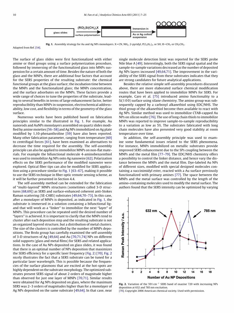
10 M. Fan et al. / Analytica Chimica Acta 693 (2011) 7–25
surface polymerization
(RO) Si(CH ) X3 2 3 Immersion in
Au or Ag colloidsuspension
glass slides
s. X = CA
Tafpgfftawiras
pnfimMtdprweetti
otRasaM“caTsostttnpchstwSA
functionalized with primary amines [77]. The space between theMNPs and the metal surface was controlled by the length of theamino-containing molecules used to modify the metal surface. Theauthors found that the SERS intensity can be optimized by varying
Fig. 1. Assembly strategy for Au and Ag NPs monolayerdapted from Ref. [54].
he surface of glass slides were first functionalized with eithermine or thiol groups using a surface polymerization procedure,ollowed by immersing of the functionalized glass into MNPs sus-ension for a certain amount of time. Besides the nature of both thelass and the MNPs, there are additional four factors that accountor the SERS properties of the resulting substrate: the chemicalunctional groups at the glass surface; the incubation time betweenhe MNPs and the functionalized glass; the MNPs concentration,nd the surface adsorbates on the MNPs. These factors provide aide range of choices to tune the properties of the substrate, lead-
ng to several benefits in terms of large enhancement factor, bettereproducibility than MNPs in suspension, electrochemical address-bility, low cost, and flexibility in terms of the geometry of the glassurface.
Numerous works have been published based on fabricationrinciples similar to the illustrated in Fig. 1. For example, Auanorods and AuNPs monolayers assembled on quartz slides modi-ed by amine moieties [56–58] and Ag NPs immobilized on Ag plateodified by 1,10-phenanthroline [59] have also been reported.any other fabrication parameter, ranging from temperature [60]
o centrifugal forces [61], have been examined as alternatives toecrease the time required for the assembly. The self-assemblyrinciple can also be applied to immobilize MNPs on non-flat mate-ials. For example the bifunctional molecule 4-aminobenzenthiolas used to immobilize Ag NPs onto Ag nanowire [62]. Polarization
ffects on the SERS performance of the modified nanowire werexplored. Optical fiber tips can also be modified for SERS applica-ion using a procedure similar to Fig. 1 [63–67], making it possibleo use the SERS technique in fiber optic remote sensing scheme, ast will be further presented in Section 4.4.
The self-assembly method can be extended for the fabricationf “multi-layered” MNPs structures (sometimes called 3-D struc-ures [68,69]) as SERS and surface-enhanced coherent anti-Stokesaman scattering (SE-CARS) substrates [49,64,70–73]. In this case,fter a monolayer of MNPs is deposited, as indicated in Fig. 1, theubstrate is immersed in a solution containing a bifunctional lig-nd that will work as a “linker” to immobilize the next “layer” ofNPs. This procedure can be repeated until the desired number of
layers” is achieved. It is important to clarify that the MNPs tend toluster after each deposition step and the resulting substrate is notn organized layered structure, but a distribution of metal clusters.he size of the clusters is controlled by the number of MNPs depo-itions. The Brolo group has carefully examined the self-assemblyf 3-D structures of Ag [49,64] and Au [70,71,74] NPs on differentolid supports (glass and metal films) for SERS and related applica-ions. In the case of Au NPs deposited on glass slides, it was foundhat there is an optimal number of NPs deposition that maximizeshe SERS efficiency for a specific laser frequency (Fig. 2) [70]. Fig. 2icely illustrates the fact that a SERS substrate can be tuned for aarticular laser wavelength. This is possible because the frequen-ies of the surface plasmons that are excited at the hot-spots areighly dependent on the substrate morphology. The optimized sub-
trates present SERS signal of about 2 orders of magnitude higherhan observed for just one layer of MNPs [70,71]. Similar resultsere obtained for Ag NPs deposited on glass, where the maximumERS was 2–3 orders of magnitudes higher than for a monolayer ofg NPs deposited on the same substrate [49,64]. In that case, near
N, NH2, 2-pyridyl, P(C6H5)2, or SH; R = CH3 or CH2CH3.
single molecule detection limit was reported for the SERS probeNile blue A [49]. Interestingly, both the SERS signal spatial and thesample-to-sample variations decreased as the number of depositedAg NPs layers increased [49,64,71]. The improvement in the vari-ability of the SERS signal from these substrates indicates that theyare strong candidates for future analytical applications.
Besides the relative simple self-assembly procedures discussedabove, there are more elaborated surface chemical modificationroutes that have been applied to immobilize MNPs for SERS. Forexample, Caro et al. [75] introduced amino functionality to aSi(1 0 0) surface using silane chemistry. The amino group was sub-sequently capped by a carboxyl alkanethiol using EDC/NHS. Thethiol group of the alkanethiol become then available to react withAg NPs. Similar method was used to immobilize CTAB-capped AuNPs on silicon wafer [76]. The use of long chain thiols to immobilizeMNPs was reported to improve sample-to-sample reproducibilityto a variation as low as 5%. The substrates fabricated with longchain molecules have also presented very good stability at roomtemperature over time.
In addition, the self-assembly principle was used to exam-ine some fundamental issues related to the SERS phenomena.For instance, MNPs immobilized on metallic substrates provideimproved SERS enhancement due to the SPs coupling between theMNPs and the metal film [77–79]. The EDC/NHS chemistry offersa possibility to control the linker distance, and hence vary the dis-tance between the MNPs and the metal film. Dye-labeled Au NPsof different sizes, modified with special designed molecules con-taining a succinimidyl ester, reacted with a Au surface previously
Fig. 2. Variation of the 591 cm−1 SERS band of oxazine 720 with increasing NPsdeposition at 632 and 785 nm excitation.[70]. Copyright 2006 American chemical society. Used with permission.
M. Fan et al. / Analytica Chimica Acta 693 (2011) 7–25 11
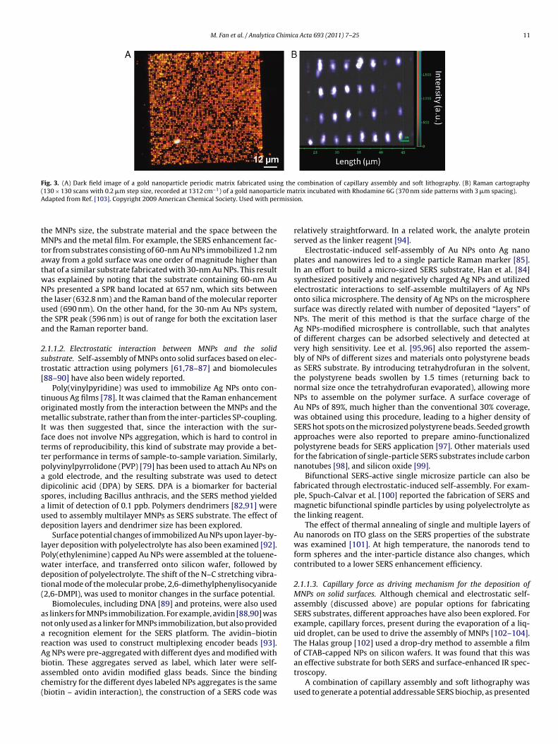
F g the( cle maA missi
tMtatwNtuta
2st[
tomIfttpadsaud
lPwdt(
anarAbac(
ig. 3. (A) Dark field image of a gold nanoparticle periodic matrix fabricated usin130 × 130 scans with 0.2 �m step size, recorded at 1312 cm−1) of a gold nanopartidapted from Ref. [103]. Copyright 2009 American Chemical Society. Used with per
he MNPs size, the substrate material and the space between theNPs and the metal film. For example, the SERS enhancement fac-
or from substrates consisting of 60-nm Au NPs immobilized 1.2 nmway from a gold surface was one order of magnitude higher thanhat of a similar substrate fabricated with 30-nm Au NPs. This resultas explained by noting that the substrate containing 60-nm AuPs presented a SPR band located at 657 nm, which sits between
he laser (632.8 nm) and the Raman band of the molecular reportersed (690 nm). On the other hand, for the 30-nm Au NPs system,he SPR peak (596 nm) is out of range for both the excitation lasernd the Raman reporter band.
.1.1.2. Electrostatic interaction between MNPs and the solidubstrate. Self-assembly of MNPs onto solid surfaces based on elec-rostatic attraction using polymers [61,78–87] and biomolecules88–90] have also been widely reported.
Poly(vinylpyridine) was used to immobilize Ag NPs onto con-inuous Ag films [78]. It was claimed that the Raman enhancementriginated mostly from the interaction between the MNPs and theetallic substrate, rather than from the inter-particles SP-coupling.
t was then suggested that, since the interaction with the sur-ace does not involve NPs aggregation, which is hard to control inerms of reproducibility, this kind of substrate may provide a bet-er performance in terms of sample-to-sample variation. Similarly,olyvinylpyrrolidone (PVP) [79] has been used to attach Au NPs ongold electrode, and the resulting substrate was used to detect
ipicolinic acid (DPA) by SERS. DPA is a biomarker for bacterialpores, including Bacillus anthracis, and the SERS method yieldedlimit of detection of 0.1 ppb. Polymers dendrimers [82,91] weresed to assembly multilayer MNPs as SERS substrate. The effect ofeposition layers and dendrimer size has been explored.
Surface potential changes of immobilized Au NPs upon layer-by-ayer deposition with polyelectrolyte has also been examined [92].oly(ethylenimine) capped Au NPs were assembled at the toluene-ater interface, and transferred onto silicon wafer, followed byeposition of polyelectrolyte. The shift of the N–C stretching vibra-ional mode of the molecular probe, 2,6-dimethylphenylisocyanide2,6-DMPI), was used to monitor changes in the surface potential.
Biomolecules, including DNA [89] and proteins, were also useds linkers for MNPs immobilization. For example, avidin [88,90] wasot only used as a linker for MNPs immobilization, but also providedrecognition element for the SERS platform. The avidin–biotin
eaction was used to construct multiplexing encoder beads [93].
g NPs were pre-aggregated with different dyes and modified withiotin. These aggregates served as label, which later were self-ssembled onto avidin modified glass beads. Since the bindinghemistry for the different dyes labeled NPs aggregates is the samebiotin – avidin interaction), the construction of a SERS code wascombination of capillary assembly and soft lithography. (B) Raman cartographytrix incubated with Rhodamine 6G (370 nm side patterns with 3 �m spacing).on.
relatively straightforward. In a related work, the analyte proteinserved as the linker reagent [94].
Electrostatic-induced self-assembly of Au NPs onto Ag nanoplates and nanowires led to a single particle Raman marker [85].In an effort to build a micro-sized SERS substrate, Han et al. [84]synthesized positively and negatively charged Ag NPs and utilizedelectrostatic interactions to self-assemble multilayers of Ag NPsonto silica microsphere. The density of Ag NPs on the microspheresurface was directly related with number of deposited “layers” ofNPs. The merit of this method is that the surface charge of theAg NPs-modified microsphere is controllable, such that analytesof different charges can be adsorbed selectively and detected atvery high sensitivity. Lee et al. [95,96] also reported the assem-bly of NPs of different sizes and materials onto polystyrene beadsas SERS substrate. By introducing tetrahydrofuran in the solvent,the polystyrene beads swollen by 1.5 times (returning back tonormal size once the tetrahydrofuran evaporated), allowing moreNPs to assemble on the polymer surface. A surface coverage ofAu NPs of 89%, much higher than the conventional 30% coverage,was obtained using this procedure, leading to a higher density ofSERS hot spots on the microsized polystyrene beads. Seeded growthapproaches were also reported to prepare amino-functionalizedpolystyrene beads for SERS application [97]. Other materials usedfor the fabrication of single-particle SERS substrates include carbonnanotubes [98], and silicon oxide [99].
Bifunctional SERS-active single microsize particle can also befabricated through electrostatic-induced self-assembly. For exam-ple, Spuch-Calvar et al. [100] reported the fabrication of SERS andmagnetic bifunctional spindle particles by using polyelectrolyte asthe linking reagent.
The effect of thermal annealing of single and multiple layers ofAu nanorods on ITO glass on the SERS properties of the substratewas examined [101]. At high temperature, the nanorods tend toform spheres and the inter-particle distance also changes, whichcontributed to a lower SERS enhancement efficiency.
2.1.1.3. Capillary force as driving mechanism for the deposition ofMNPs on solid surfaces. Although chemical and electrostatic self-assembly (discussed above) are popular options for fabricatingSERS substrates, different approaches have also been explored. Forexample, capillary forces, present during the evaporation of a liq-uid droplet, can be used to drive the assembly of MNPs [102–104].The Halas group [102] used a drop-dry method to assemble a film
of CTAB-capped NPs on silicon wafers. It was found that this wasan effective substrate for both SERS and surface-enhanced IR spec-troscopy.A combination of capillary assembly and soft lithography wasused to generate a potential addressable SERS biochip, as presented

12 M. Fan et al. / Analytica Chimic
FtC
inwnNTt“scoN
tbdsor
2pmgBltmiNosd
baraaSsttdF
Other figures of merit, such as the detection limit, have been
ig. 4. SERS spectra of Rhodamine 6G (R6G) on Ag nanoparticle film at differentemperatures. The R6G concentration was 10−5 M [110]. Copyright 2005 Americanhemical Society. Used with permission.
n Fig. 3 [103]. A pre-fabricated PDMS stamp was placed under-eath a glass slide. Au NPs solutions were injected, and the stampas pulled away relative to the glass slide, leading to a specificumber of NPs being assembled on the patterns of the stamp. ThePs pattern was transferred onto amine functionalized glass slides.he SERS properties were shown to depend on the number of NPs inhe aggregates. A slightly different approach, named by the authorswrinkle-confined drying”, was developed to assemble Au NPs intoingle/double-(particle)-line arrays on glass support [105]. In thisase, the PDMS was firstly stretched to form winkles, following byxygen plasma hardening. This stamp was then used to confine AuPs on glass supports.
Convective techniques were used to assemble Ag NPs and bac-eria cells together on a glass support, allowing the detection of theacteria by SERS [104]. Two glass slides were set at an angle of 24egrees and the NPs and bacteria mixture was dropped between thelides. One of the slides was set to move slowly yielding a thin filmf the mixture at the end of the process. This procedure resulted ineproducible SERS detection of very small amounts of bacterias.
.1.1.4. Direct transfer of pre-assembled MNPs film to a solid sup-ort. Immobilized MNPs can also be obtained by transferring MNPsonolayers from a liquid–liquid interface to a solid support, usually
lass or silicon wafer [106–109], using, for instance, the Langmuir-lodgett technique. This procedure is known to provide good single
ayer structures [107], and the technique was also used to examinehe effect of multiple layers of Au spherical NPs, nanorods and their
ixtures on the SERS efficiency of the substrate [106]. The resultsndicated that the SERS signal increased with increasing layers ofPs, and that nanorods films are more SERS efficient than filmsf spherical NPs. Experiments with mixed layers of nanorods andpherical MNPs showed that the ultimate enhancement was mainlyecided by the top layer.
The size effect of the Au NPs on the SERS enhancement has alsoeen explored using substrates prepared by the Langmuir–Blodgettpproach [108]. It was found that immobilized 25 nm Au NPsesulted in the best substrate (other sizes examined were 16, 40nd 70 nm). One of the most interesting SERS substrates built fromliquid–liquid interface is probably the temperature-controlled
ERS substrate (Fig. 4) [110]. The NPs were first assembled at waterurface and transferred through the Langmuir-Blodgett technique
o a temperature-responsive polymer membrane. R6G SERS spec-ra on such a substrate at different temperature were recorded toemonstrate the tunable plasmon coupling capability, as shown inig. 4.a Acta 693 (2011) 7–25
2.1.2. Chemically and photochemically grown MNPs on solidsupports
MNPs can be chemically grown on a solid support [111], syn-thesized in a polymer film [112], or in block copolymers [113]. Forexample, Ag NPs of ∼100 nm diameter can be grown on the sur-face of silicon wafers from mixtures of hydrofluoric acid and silvernitrate solutions, and used as SERS substrates [114]. Photo-reaction[115,116] was also used to immobilize Ag NPs on optical fiber, afterthe fiber tip was immersed in a mixture of aqueous silver nitrateand sodium citrate solutions.
The chemical or photochemical procedure can also be usedto further modify/grow self-assembled MNPs that were previ-ously deposited as “seeds”. The further treatment of self-assembledAu/Ag alloy NPs on silicon substrate with HAuCl4 solution had asignificant effect on the SERS enhancement efficiency [117]. Theauthors attributed the initial increase in SERS enhancement to theformation of pin-holes on the assembled alloy NPs. Further increaseof the incubation time of the substrate with the HAuCl4 solutionled to the disappearance of the pin-holes and decreased the SERSintensity. A systematic examination of the effect of an Ag enhancer,a silver ions solution that promoted the growing of Ag on a SERSsubstrate, on self-assembled Au NPs on glass surfaces was reported.An optimized time for the application of the Ag enhancer was pro-posed [118]. Similarly, Ag enhancer was also used to modify Au NPsarrays fabricated by in situ growing in block copolymers, and it wasfound that not only the enhancement, but also the reproducibilityincreased as well [113].
A very special example of in situ chemical growth of MNPs forSERS was reported by Whitcomb et al. [119]. In this case, Ag NPsclusters were generated thermally by initiating the reduction ofsilver carboxylates into thin polymer films used in diagnostic radio-graphy. It was found that the Ag NPs synthesized from this approachcan also be used as SERS substrate to investigate the chemistryrelated to the imaging process. This type of SERS substrate fabri-cation method may be useful for investigating catalytic reactionsinside polymers.
2.1.3. Other methodsBy evaporating a phosphate buffer solution of Ag NPs, Kumar
et al. [120] found that the NPs aggregates found at the trough of thesalts well could serve as SERS substrate for biomolecule detection.
2.2. Evaluation – reported EFs, and other figures of merits
The SERS average enhancement factor (EF) is generally quotedas an indicator of the quality of a new SERS substrate. However,it is important to point out that the EFs are generally estimatedthrough several approximations. Moreover, they might depend onother factors, such as the molecular system used in the estimationand the excitation wavelength. Therefore, the reader is advised toexercise caution when comparing these numbers from differentsubstrates. For instance, the very first report of self-assembly MNPson solid report by Freeman et al. [54] quoted an EF of 105. However,it should be pointed out that this was achieved after chemicallydepositing Ag film on top of the assembled Au NPs, which is knownto enhance the SERS efficiency [118]. In general, the average EFsreported for immobilized MNPs ranges from 104 [76,103,121,122]to 107 [57,114,123]. Although larger EFs are sometimes claimed,such as the SERS-EF of 1010 indicated in Ref. [124], these unusualhigh average EFs are seldom reproduced or confirmed by differentgroups.
used to evaluate MNPs-deposited SERS substrates. For example,for proteins, a near single molecule detection limit was reported[125]. Our group demonstrated that a self-assembled substrate fab-ricated by 7 depositions of Ag NPs, as described in Section 2.1.1,

himica Acta 693 (2011) 7–25 13
prisSeToseids1ts
3n
dasstpar
3
locpbsrircn
cctlilsaSpFtS(ts
sdt
Fig. 5. Schemes for two fabrication strategies for SERS substrates using EBL. Twoprocesses are presented. The left hand side process consists in an chemical etchingthat follows the electron beam exposing, the dissolution of the remaining PMMAlayer, and deposition of metal. The substrate ends up with metal over the wholesurface. The right hand side shows a metal deposition immediately after the e-beam
M. Fan et al. / Analytica C
resent a near single-molecule detection limit for nile blue A underesonance Raman conditions [49]. Reproducibility, including SERSntensity spatial variations in planar substrates and sample-to-ample variations, is another major concern in the development ofERS substrate. Freeman et al. reported an spatial variation in SERSfficiency between 5% and 8% for their solid-supported MNPs [54].he reproducibility of the SERS signal was shown to be dependentn the number of MNPs depositions for the self-assembled sub-trates [49,71]. It was found that not only the SERS enhancementfficiency, but also the spatial and sample to sample reproducibilityncreases with the deposition number. The spatial relative standardeviation (RSD%) and the sample to sample variation of the SERSignal can be less than 20% for “multi-layered” structures. RSD% of0% [76], 15% [118] and 10–20% [76] for the SERS intensities spa-ial variation has been reported for other MNPs supported on solidurfaces substrates.
. Metallic nanostructures Fabricated usinganolithographic methods
This section will cover the SERS substrates obtained byirectly fabricating metallic nanostructures on a solid support. Thispproach is generally classified as “top down”, in contrast to theelf-assembled (“bottom up”) methods covered in Section 2. For theake of organization, the first topic of this section will cover mostlyhe nanolithographic methods, including electron-beam lithogra-hy. The subsequent topics will cover the advances in fabricationnd application in SERS for two specific classes of substrates: theegular arrays of MNPs; and nanoholes arrays on metallic thin films.
.1. Electron beam lithography
One of the most used nanolithographic method is electron beamithography (EBL). The EBL technique consists of a 10–50 keV beamf electrons focused on a solid support, generally electronresist-overed SiOx/Si wafers. As in regular photolithography, EBL can beerformed using either positive or negative resists. The electroneam selectively etches off regions of the positive resist from theurface in a predetermined form. In contrast, the region exposedemains if a negative resistor is used. The most used electronresists by far poly(methyl methacrylate) (PMMA), which is a positive EBLesistor. Generally, after the EBL etching of PMMA, there are twoommonly follow-up procedures for the synthesis of SERS-activeanostructures, both schematically depicted in Fig. 5 [51].
In the left-hand side of Fig. 5, after the EBL procedure follows ahemical etching of the SiOx/Si surface using HF containing baths,ausing an increase in the depth of the exposed features. Removinghe remaining photoresist with a developer and depositing a metalayer results in a nano-patterned metallic film. A second approachs depicted in the right-hand side of Fig. 5: the metal deposition fol-ows the EBL procedure and additional exposition to the removerolution peels off the remaining photoresist and the metallic layerttached to it (lift-off); as a result discrete MNPs attached to theiOx/Si support are available for the SERS measurements. The SERSerformances of both MNPs construction approaches depicted inig. 5 have been evaluated for gold, and it was found that the con-inuous films approach (left hand side in Fig. 5) leads to a betterERS performance when compared to the discrete MNPs substratelift off procedure in Fig. 5) [51]. The better SERS performance ofhe continuous films was assigned to the presence of several sharp
urfaces in the breaks of this substrate.The most important advantage of the EBL approach is the pos-ibility of control the MNPs size and shape and the interparticleistance with great accuracy [126–128]. Gunnarsson et al. exploredhe distance control in the evaluation of the distance-dependent
exposition. After removal of the photoresistor layer, the substrate will present aseries of isolated NPs, separated by regions where only bare Si substrate is exposed.From Kahl et al. [51]. Copyright: 1998 Elsevier Science S.A. Used with permission.
SERS performance for circular and triangular silver NPs with200 nm diameter (for the circular and edge length for the trian-gles) as constant dimension [129]. The SERS intensity showed a60-fold decrease with the increase in the circular inter-particle dis-tance from 75 to 205 nm for thiophenol as the probe molecule.These results were well fitted by an electrostatic model, and theauthors suggested that the main contribution to SERS enhancementon these nanostructures is due to the edges of the structures andthe induced polarization between the structures. In a similar exper-iment, Liu et al. reported 100 nm in diameter Au nanoposts as theSERS substrate [130], and used finite difference time domain (FDTD)numerical calculations that confirmed previous suggestions [129].
Yu et al. compared the SERS performance of Au nanodisksand nanoholes fabricated by EBL as a function of the separa-tion and dimensions of the nanostructures [131]. In addition tothe trend of increase in SERS performance as the nanostructureswere fabricated closer to each other, the authors also noticed thatthe nanodisks presented an increase in SERS performance as thedimensions of the features decreased; an opposite trend comparedto the nanoholes. The nanoholes array with the best SERS perfor-mance, which had the diameter of 370 nm and the grating pitchof 500 nm, presented a SERS-EF of 4 × 10⁵; the best performancenanodisks array had dimension of 60 nm in diameter and gratingpitch of 100 nm, and presented a SERS-EF of 1 × 10³. The better per-formance presented by the nanoholes arrays was attributed to theseveral degrees of coupling between holes, which was not to beobserved in the nanodisks arrays.
Aperiodic nanostructures obtained by EBL with additionalnanostructures of dimensions around 30 nm have been inves-tigated [132]. The modification was directed by the local fieldenhancement, and resulted in 30 nm nanostructures connectedto the 200 nm features obtained by FIB. The claimed spatially-averaged SERS-EF on these substrates was ca. 108, 3 orders ofmagnitude higher than the original nanostructures. The increasein SERS performance may be attributed to the coupling of the
additional nanostructures with the neighboring nanostructures, assuggested by FDTD numerical calculations reported by the authors.The approach of EBL-constructed aperiodic arrays of SERS-activeMNPs was also used for the creation of matrices of randomly dis-tributed MNPs with several shapes and sizes [133]. Each matrix has
14 M. Fan et al. / Analytica Chimica Acta 693 (2011) 7–25
Fig. 6. (a) 3-D finite-difference time-domain simulation results showing significant field intensity enhancement within a 5 nm nanogap. (b) Fabrication process schematicof the nanogap array. Starting from patterned substrates, the secondary metal layer is separated by a thin alumina spacer deposited using atomic layer deposition. Usings aluma in paeF sion.
bdotai
beopfiatdto
sswol
idewall spacer processing, the nanogap size is determined by the thickness of thecircular pattern. (d) The magnified image of a single ring-shaped element shown
lement.rom Im et al. [135]. Copyright 2010 American Chemical Society. Used with permis
een reproduced 10 × 10 times in a solid support, and the depen-ence of SERS performance on the surface coverage by MNPs, andn MNPs shapes, sizes and interconectivity was studied. The con-rol over the three previous parameters allowed the authors tochieve reproducible substrates presenting SERS-EF of 5 × 10⁸, fornterconnected prolates/oblates structures.
A very high average SERS-EF of 109 have been reported for EBL-ased SERS substrates obtained with an angle deposition techniquemployed by Theiss et al. [134]. The features fabricated were dimerf MNPs with a separation of ca. 1 nm, obtained by a double maskrocedure, and the deposition of two metallic layers at two dif-erent angles. The first deposition is normal to the support, and its followed by a controlled change in the angle of deposition. Thengle of second deposition results in a second NP at a distance fromhe first that may be tuned by the deposition angle. Interparticleistances as small as 1 nm have been reported, and such short dis-ances are to account for the reported very high SERS-performancef these substrates.
In addition to EBL, optical lithography was used to obtain
tructures with metallic features with controlled nanogaps, aschematically shown in Fig. 6 [135]. After the optical lithographyriting of a gold surface, an ultrathin (5–20 nm) continuous filmf alumina was deposited on the microstructures by an atomic-ayer deposition (ALD) method. An additional layer of metal was
ina layer. (c) Scanning electron microscopy (SEM) image of a nanogap array withnel c. (e) The magnified image of a 10 nm nanogap formed along the ring-shaped
evaporated on the alumina layer. The added metallic layer was fur-ther milled out by either optical lithography or FIB, exposing partof the alumina layer, which was etched out by a buffered oxideetchant commercial solution. The resulting structures, shown inFig. 6C–E, present nanogaps with thickness that depends on thealumina layer deposited. The SERS performance of this sort of sub-strate was shown to be better than the Ag-film over nanosphere(FON) substrate (to be discussed in Section 3.3), with an averageSERS-EF of 107, with a maximum of 109, for the substrates with5 nm wide nanogaps.
3.2. Nanoparticle arrays
The preparation of nanoparticle arrays with controllable sizeand nanoparticle coverage are advantageous as SERS substratesin microfluidic devices. The small area of the SERS active sur-face allows for device miniaturization and the use of severalsampling regions in the same substrate, without interferencebetween different arrays. The micro-contact printing technique
has been used to fabricate microarrays of Ag NPs. A chemicallymodified poly(dimethyl siloxane) (PDMS) patterned substrate wasexposed to Ag colloidal suspension, and the adsorbed colloid wheretransferred to 4-mercaptopyridine or aminoethanethiol modifiedAu-coated silicon substrate [136]. The resulting substrates pre-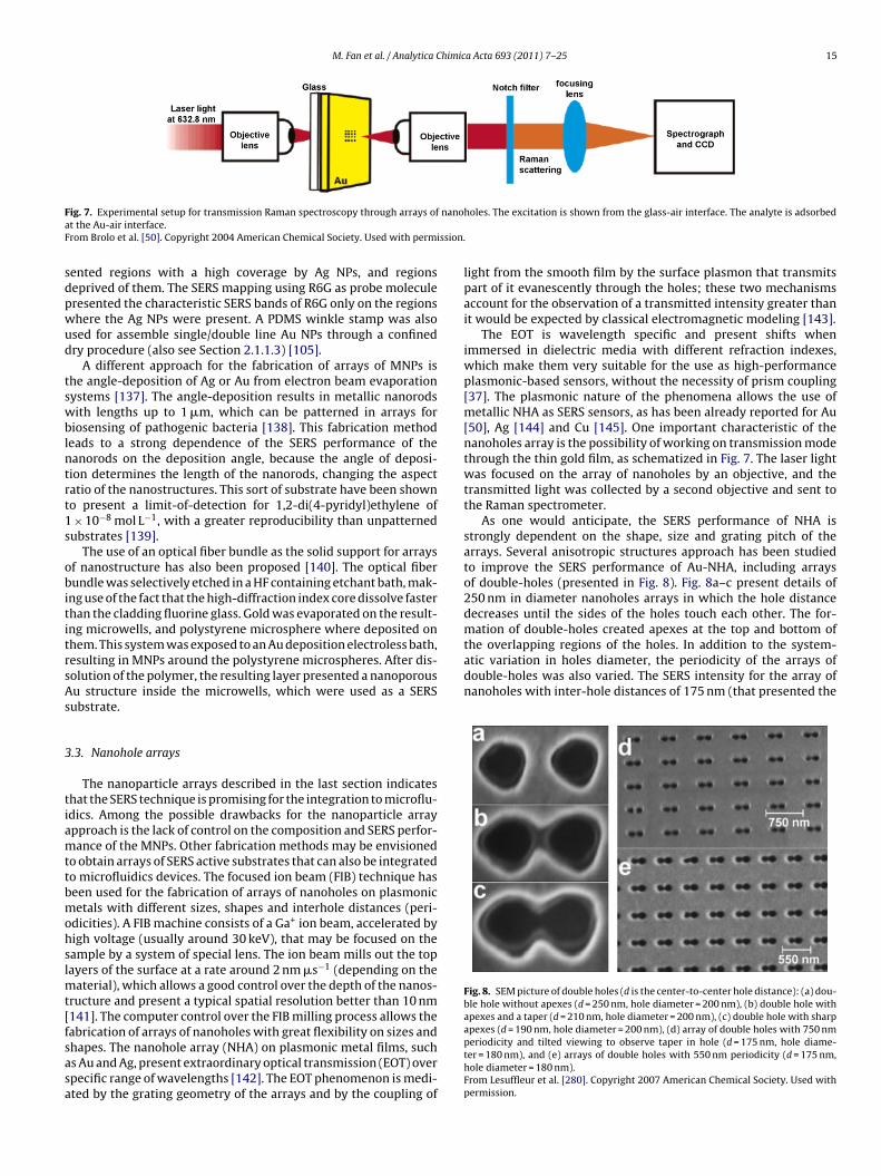
M. Fan et al. / Analytica Chimica Acta 693 (2011) 7–25 15
F nanoaF ssion.
sdpwud
tswblntrt1s
obititrsAs
3
tiamttbmohslmt[fsasa
mation of double-holes created apexes at the top and bottom ofthe overlapping regions of the holes. In addition to the system-atic variation in holes diameter, the periodicity of the arrays ofdouble-holes was also varied. The SERS intensity for the array ofnanoholes with inter-hole distances of 175 nm (that presented the
Fig. 8. SEM picture of double holes (d is the center-to-center hole distance): (a) dou-ble hole without apexes (d = 250 nm, hole diameter = 200 nm), (b) double hole withapexes and a taper (d = 210 nm, hole diameter = 200 nm), (c) double hole with sharp
ig. 7. Experimental setup for transmission Raman spectroscopy through arrays oft the Au-air interface.rom Brolo et al. [50]. Copyright 2004 American Chemical Society. Used with permi
ented regions with a high coverage by Ag NPs, and regionseprived of them. The SERS mapping using R6G as probe moleculeresented the characteristic SERS bands of R6G only on the regionshere the Ag NPs were present. A PDMS winkle stamp was alsosed for assemble single/double line Au NPs through a confinedry procedure (also see Section 2.1.1.3) [105].
A different approach for the fabrication of arrays of MNPs ishe angle-deposition of Ag or Au from electron beam evaporationystems [137]. The angle-deposition results in metallic nanorodsith lengths up to 1 �m, which can be patterned in arrays for
iosensing of pathogenic bacteria [138]. This fabrication methodeads to a strong dependence of the SERS performance of theanorods on the deposition angle, because the angle of deposi-ion determines the length of the nanorods, changing the aspectatio of the nanostructures. This sort of substrate have been showno present a limit-of-detection for 1,2-di(4-pyridyl)ethylene of× 10−8 mol L−1, with a greater reproducibility than unpatterned
ubstrates [139].The use of an optical fiber bundle as the solid support for arrays
f nanostructure has also been proposed [140]. The optical fiberundle was selectively etched in a HF containing etchant bath, mak-
ng use of the fact that the high-diffraction index core dissolve fasterhan the cladding fluorine glass. Gold was evaporated on the result-ng microwells, and polystyrene microsphere where deposited onhem. This system was exposed to an Au deposition electroless bath,esulting in MNPs around the polystyrene microspheres. After dis-olution of the polymer, the resulting layer presented a nanoporousu structure inside the microwells, which were used as a SERSubstrate.
.3. Nanohole arrays
The nanoparticle arrays described in the last section indicateshat the SERS technique is promising for the integration to microflu-dics. Among the possible drawbacks for the nanoparticle arraypproach is the lack of control on the composition and SERS perfor-ance of the MNPs. Other fabrication methods may be envisioned
o obtain arrays of SERS active substrates that can also be integratedo microfluidics devices. The focused ion beam (FIB) technique haseen used for the fabrication of arrays of nanoholes on plasmonicetals with different sizes, shapes and interhole distances (peri-
dicities). A FIB machine consists of a Ga+ ion beam, accelerated byigh voltage (usually around 30 keV), that may be focused on theample by a system of special lens. The ion beam mills out the topayers of the surface at a rate around 2 nm �s−1 (depending on the
aterial), which allows a good control over the depth of the nanos-ructure and present a typical spatial resolution better than 10 nm141]. The computer control over the FIB milling process allows the
abrication of arrays of nanoholes with great flexibility on sizes andhapes. The nanohole array (NHA) on plasmonic metal films, suchs Au and Ag, present extraordinary optical transmission (EOT) overpecific range of wavelengths [142]. The EOT phenomenon is medi-ted by the grating geometry of the arrays and by the coupling ofholes. The excitation is shown from the glass-air interface. The analyte is adsorbed
light from the smooth film by the surface plasmon that transmitspart of it evanescently through the holes; these two mechanismsaccount for the observation of a transmitted intensity greater thanit would be expected by classical electromagnetic modeling [143].
The EOT is wavelength specific and present shifts whenimmersed in dielectric media with different refraction indexes,which make them very suitable for the use as high-performanceplasmonic-based sensors, without the necessity of prism coupling[37]. The plasmonic nature of the phenomena allows the use ofmetallic NHA as SERS sensors, as has been already reported for Au[50], Ag [144] and Cu [145]. One important characteristic of thenanoholes array is the possibility of working on transmission modethrough the thin gold film, as schematized in Fig. 7. The laser lightwas focused on the array of nanoholes by an objective, and thetransmitted light was collected by a second objective and sent tothe Raman spectrometer.
As one would anticipate, the SERS performance of NHA isstrongly dependent on the shape, size and grating pitch of thearrays. Several anisotropic structures approach has been studiedto improve the SERS performance of Au-NHA, including arraysof double-holes (presented in Fig. 8). Fig. 8a–c present details of250 nm in diameter nanoholes arrays in which the hole distancedecreases until the sides of the holes touch each other. The for-
apexes (d = 190 nm, hole diameter = 200 nm), (d) array of double holes with 750 nmperiodicity and tilted viewing to observe taper in hole (d = 175 nm, hole diame-ter = 180 nm), and (e) arrays of double holes with 550 nm periodicity (d = 175 nm,hole diameter = 180 nm).From Lesuffleur et al. [280]. Copyright 2007 American Chemical Society. Used withpermission.

16 M. Fan et al. / Analytica Chimica Acta 693 (2011) 7–25
Fig. 9. SERS intensity maps (a and b) recorded with the incident light polarized as indicated. “Vertical” and “horizontal” refer to the orientation of the electric vector of thelight with respect to the nanowire raft whose optical image is shown in the upper right-hand corner. Typical SERS spectra recorded at the locations indicated are shown att aseline of theaA ith pe
sfot
FRbA
he right of each of the SERS intensity maps. The maps were produced using the bxcited with 514.5-nm Ar ion laser light. Note the strong polarization dependencecross the nanowires.dapted from Jeong et al. [42]. Copyright 2004 American Chemical Society. Used w
harpest apexes in that particular study) was 12 times greater thanor an array with the separation of 250 nm, which presented noverlapping between holes. The optimization of the periodicity ofhe 175 nm hole-separation arrays (with the optimized value of
ig. 10. Left-hand side: SEM images of the Au substrates obtained using as templates PCight-hand side: SERS spectra of the probe molecule 4-MPy on different SERS substratesar corresponds to the spatial variation obtained from each substrate.dapted from Batista et al. [43]. Copyright 2009 American Scientific Publishers. Used wit
e-corrected intensities of the 1649 cm−1 Raman band of R6G. Raman spectra wereSERS spectra with the strongest signal obtained when the laser light is polarized
rmission.
490 nm for periodicity) resulted in additional 12.4 times in the SERSenhancement.
Further optimization of anisotropic nanoholes presents the pos-sibility of improving the SERS performance of the substrate. The use
Ms with different pore diameters.(A) 400 nm; (B) 200 nm; (C) 100 nm; (D) 50 nm.. The ring breathing bands at ca. 1000 cm−1 are shown in the same scale. The error
h permission.

M. Fan et al. / Analytica Chimica Acta 693 (2011) 7–25 17
F d c) std 0 nm,F
olacpstatb6l
4
f
FC
ig. 11. SEM images of: (a) an electrochemically roughened gold surface and (b aniameter template spheres and have thickness of (a) 150 nm, (b) 260 nm and (c) 46rom Abdelsalam et al. [154]. Copyright 2005 Elsevier. Used with permission.
f concentric circles in plasmonic has been studied to increase theocal field concentration on the center of the structure; this char-cteristic was used in conjunction of a double-hole structure toreate a SERS substrate that presents good performance and laser-olarization dependence [146]. The symmetry of the double-holetructure resulted in strong polarization dependence. The excita-ion of the structure using a polarization perpendicular to the longxis of the double-hole resulted in stronger field localization onhe nanostructure apex, leading to higher SERS intensity. The num-er of molecules calculated to be in the apex (responsible for ca.0% of the SERS intensity) was ca. 1300, leading to an estimated
imit-of-detection of 20 molecules.
. Template techniques
Control over the morphology of the nanostructures is requiredor the SERS technique to reach a new level of applicability in
ig. 12. Ag NPs fabricated through the NSL technique [165] left, single layer mask particlhemical Society. Used with permission.
ructured gold surfaces. The structured gold surfaces were produced using 600 nmrespectively. The scale bar is 2 �m in each case.
analytical sciences. Recent advances in both self-assembly (Sec-tion 2) and nanofabrication (Section 3) have helped to overcomethe reproducibility issues for several types of substrates. However,the most reproducible structures prepared by EBL and FIB, cannotbe mass produced using those methods. The use of templates thatallow the deposition of metals with controlled geometry is one ofthe most promising approaches to overcome such challenges. Thetemplate directed synthesis is a broad field of study, and this reviewwill depict the principles of only two of the most used templatedeposition strategies: electrochemical and vapour deposition.
4.1. Electrochemical depositions
Electrochemical deposition of metals in anodic alumina oxide(AAO) substrates, also also known as porous anodic alumina(PAA) membranes, has been explored for the creation of high-performance SERS substrates. The AAO substrates may be obtained
e arrays; right, AFM image of the Ag triangles fabricated. Copyright 2001 American

18 M. Fan et al. / Analytica Chimica Acta 693 (2011) 7–25
F opyrigp ith pe
bindatAedsaTant
A
ig. 13. (a) Schematic representation of Vo-Dinh’s DNA detection scheme [196] Carticle-on-wire system [197]. Copyright 2009 American Chemical Society. Used w
y high-voltage dissolution of alumina in acid solutions. The result-ng structure presents a honeycomb-like arrangement, with tens ofanometers diameter pores arranged in a hexagonal packing. Theiameter of the pores is controlled by the applied voltage, type ofcid bath and temperature, and the pores depth is controlled byhe dissolution time [147]. It is also possible to find commerciallyAO membranes that are suitable for the deposition of metals. Thelectrodeposition of metals is carried out by alternating currenteposition at voltages in the 10–25 V range. The metal electrodepo-ition is followed by dissolution of the alumina layer in a phosphoriccid bath, which releases free nanorods or nanotubes of the metal.
he resulting metallic nanostructures may have a high aspect rationd present a high SERS performance [148]. It is interesting tootice that the procedure described above result in collapsing ofhe nanowires. If the dissolution of the AAO layer is complete, theFig. 14. Multilayer Ag NPs modifieddapted from Ref. [64]. Copyright 2010 Elsevier Science. Used with permission.
ht 2003 ACS. (b) schematic representation for the detection of target DNAs by Aurmission.
metallic nanowires are going to be found free in suspension of theetchant and can be recovered from it. It has been determined thatthe maximum SERS performance for Ag nanowires synthesized onAAO is for the 95 nm in diameter nanowires for 632.8 nm excitingradiation, and that the performance improves as the aspect ratioincreases [149].
The metallic nanowires tend to form bundles when completelyreleased from the PAA template, which creates very narrow gapsbetween them (in the order of 1–4 nm), improving significantlythe SERS performance. The SERS performance of the resultingnanowires is strongly polarization dependent, due to their usually
high aspect ratio. A demonstration of the polarization dependenceof the SERS intensity in Ag nanowires is presented in Fig. 9. TheSERS intensity enhancement when the laser polarization was par-allel to the long-axis of the nanowires bundle was 10 times smallerhighly sensitive SERS optrode.

himic
tadeSn
fai[dPmtafFPcthfbiocent
utrsToosatlsomtsP
tsomtadwrpbteb[
c
M. Fan et al. / Analytica C
han when the laser polarization was perpendicular to the long-xis of the nanowire bundles. These results show that the inducedipole between nanowires plays a significant role in the SERSnhancement for these substrates. The polarization dependence ofERS intensity have also been observed for Ag-NPs decorated Aganowires [62].
Polycarbonate membranes (PCM) can also be used as templatesor the electrodeposition of metal nanowires and nanotubes. PCMre obtained by exposing a smooth membrane to highly chargedons, such as Ar ions, with acceleration energy around 5.5 MeV u−1
150]; these membranes are also commercially available with poreiameters varying in the range of 20–500 nm. The nanopores ofCMs have been shown to be suitable for electrodeposition ofetals such Ni, Fe, Pt, Au and Ag [151]. Gold electrodeposited on
he nanopores have been used as SERS substrates. The nanowiresnd nanotubes obtained and the corresponding SERS performanceor the detection of 4-mercaptopyridine (4-MPy) are presented inig. 10 [43]. The deposition was performed galvanostatically onCM with holes of 400, 200, 100 and 50 nm in diameter, with aurrent density of 500 �A cm−2 for all membranes. After dissolu-ion of the PCM, the structures obtained from the 400 and 200 nmoles membranes were nanotubes, but nanowires were obtained
or the 100 and 50 nm holes membranes. These differences haveeen attributed to different growth velocity in vertical and hor-
zontal direction for different nanopores. The SERS performancef the nanowires with 50 nm in diameter has been shown to beonsiderably higher than both the other PCM membranes and anlectrochemically roughened gold electrode. Specifically, the 50 nmanowires presented an estimated SERS-EF of 1.3 × 10⁷, comparedo 3.7 × 10⁶ for the electrochemically roughened Au electrode.
Polystyrene microspheres (PSM) have also been extensivelysed as templates for the electrodeposition of SERS-active nanos-ructures [44,152]. The PSM are commercially available in a wideange of sizes, and the self-assembly of these microparticles fromuspension on solid supports is a well established method [153].he template of PSM is created by self-assembling the microspheresn a conducting solid support. The methods for the self-assemblyf PSM may involve the spin-coating of the suspension on the sub-trate, or drying off the suspension using controlled temperaturend humidity on the process. The PSM layer may be controlled byhe velocity of the evaporation of the solvent or by dip-coating,eading to one or more monolayers of microspheres on top of theolid support. The template assembly is followed by immersionn a deposition bath containing the necessary metallic ions foretal electrodeposition. The deposition charge is used to control
he thickness of the metallic nanostructures. Fig. 11 Shows typicaltructures obtained from gold deposition over one monolayer thickSM [154].
The SERS performance of the gold nanostructures obtained fromhe electrodeposition on PSM template have been systematicallytudied as a function of microsphere diameter and of the thicknessf the deposited Au film [44]. For a 633 nm laser excitation, theaximum SERS-EF of 6.6 × 10⁸ has been claimed for a silver film
hickness of 140 nm on a PSM layer of 350 nm in diameter. The rel-tive SERS performance of substrates fabricated with different PSMiameters and metal film thickness have been directly comparedith the reflectance spectra of the structures, and the minimum in
eflectance were correlated with the excitation of localized surfacelasmon resonances. It has been verified that the substrate withest SERS performance presented the excitation and Raman scat-ered frequencies within the LSPR band, which is expected from the
lectromagnetic mechanism. Recently, it has been shown that PSMased SERS templates can be used for single-molecule detection155].Block copolymers have also been used as template for electro-hemical deposition (plating) of gold as large area SERS substrates
a Acta 693 (2011) 7–25 19
[152]. The advantage of using block copolymers is that nanostruc-tures smaller than 100 nm with a, which are superior in terms ofSERS performance, can be easily fabricated.
4.2. Vapor deposition
SERS substrate can be obtained by directly vapor depositing thinlayers of metals on solid supports [55]. When the metal thickness issmall (∼10 nm in case of Ag), the evaporated metal tend to cluster,forming islands/particles instead of a flat film. Such kind of proce-dure has been widely used for the fabrication of SERS substrates ondifferent materials, such as optical fibers [156] and nano-structuredoptical fiber bundles [157–161].
Ag nanorods can also be obtained through a process calledoblique angle deposition (OAD) technique [162,163]. This methodconsists of setting the substrate tilted relative to the incoming metalvapor, resulting on 500 nm long Ag nanorods with a aspect ratiosof around 5 [163].
One of the most common type of vapor deposited SERS sub-strates was developed by the Van Duyne group [36,164], in aprocess known as nanosphere lithography (NSL) [165] (Fig. 12).The method consists on self-assembling a layer of nanosphereson a solid support, following by the vapor deposition of metals,such as Ag, directly on the layer of nanospheres. The nanospheresare then coated by a rough metallic structure that already can beused for SERS measurement (FON substrate) [164]. However, inNSL a further step is performed to remove the nanosphere maskSince the metal is deposited through the interstices of the layer ofnanospheres, a periodic nanostructures of triangles and hexagonscan be formed (depending if one or two layers of nanosphere maskwas used) [166–168]. It was found that both the in plane and the outof plane diameters of the periodic structure obtained after removalof the mask can be carefully controlled. The Van Duyne group [169]was able to examine the relationship between the LSPR extinctionmaximum and the SERS enhancement factor using this substrateand an EF of 108 has been reported.
The necessity for a highly reproducible SERS substrate moti-vated the use of visible light lithography on Si supports in thedevelopment of a commercially viable SERS substrate. The pho-tolithography resulted in conic micro-wells with 2 �m pitch; Goldwas evaporated on the drawn Si substrate. The resulting sub-strate presents highly reproducible SERS performance and it hasbeen patented by the authors [170,171]. This substrate had beencommercially available initially by a spin-off enterprise by theUniversity of Southampton under the designation of KlariteTM;nowadays it is marketed by the Renishaw, Inc. Although theKlariteTM substrate does not present a SERS-EF in the cutting-edgeof SERS substrates, the high reproducibility allowed the applicationof this substrate in several problems in several areas such as molec-ular monolayer orientation of organothiols [172] and to improvefluorescence emission rate of immunoassay related fluorophores[173] among others [174].
5. Applications
Since its discovery in 1970s [13,15], SERS is becoming moreattractive for applications. Several factors is contributing to this“popularization” of the SERS method, including the advent ofseveral new types of Raman systems, from modern microscopesto miniaturized spectrometers, and the fast paced advances on
the development of substrates, as discussed in Sections 2–4 ofthis review. Nowadays, SERS has moved far beyond its originalform as a technique to investigate the surface adsorption at elec-trode surfaces. SERS is today one of the most sensitive analyticaltechniques, and it is fast moving from fundamental research to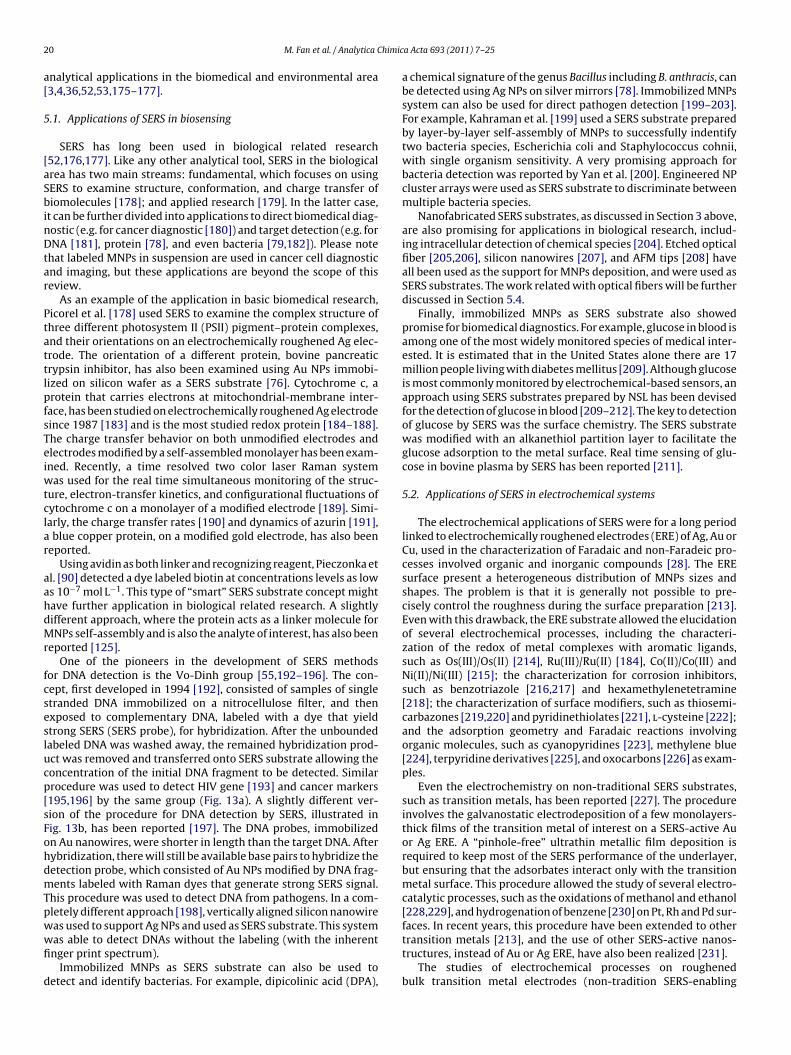
2 himic
a[
5
[aSbinDtar
PtattlpfsTeiwtclar
aahdMr
fcseslucp[sFohdmTpwwfi
d
0 M. Fan et al. / Analytica C
nalytical applications in the biomedical and environmental area3,4,36,52,53,175–177].
.1. Applications of SERS in biosensing
SERS has long been used in biological related research52,176,177]. Like any other analytical tool, SERS in the biologicalrea has two main streams: fundamental, which focuses on usingERS to examine structure, conformation, and charge transfer ofiomolecules [178]; and applied research [179]. In the latter case,
t can be further divided into applications to direct biomedical diag-ostic (e.g. for cancer diagnostic [180]) and target detection (e.g. forNA [181], protein [78], and even bacteria [79,182]). Please note
hat labeled MNPs in suspension are used in cancer cell diagnosticnd imaging, but these applications are beyond the scope of thiseview.
As an example of the application in basic biomedical research,icorel et al. [178] used SERS to examine the complex structure ofhree different photosystem II (PSII) pigment–protein complexes,nd their orientations on an electrochemically roughened Ag elec-rode. The orientation of a different protein, bovine pancreaticrypsin inhibitor, has also been examined using Au NPs immobi-ized on silicon wafer as a SERS substrate [76]. Cytochrome c, arotein that carries electrons at mitochondrial-membrane inter-ace, has been studied on electrochemically roughened Ag electrodeince 1987 [183] and is the most studied redox protein [184–188].he charge transfer behavior on both unmodified electrodes andlectrodes modified by a self-assembled monolayer has been exam-ned. Recently, a time resolved two color laser Raman system
as used for the real time simultaneous monitoring of the struc-ure, electron-transfer kinetics, and configurational fluctuations ofytochrome c on a monolayer of a modified electrode [189]. Simi-arly, the charge transfer rates [190] and dynamics of azurin [191],blue copper protein, on a modified gold electrode, has also been
eported.Using avidin as both linker and recognizing reagent, Pieczonka et
l. [90] detected a dye labeled biotin at concentrations levels as lows 10−7 mol L−1. This type of “smart” SERS substrate concept mightave further application in biological related research. A slightlyifferent approach, where the protein acts as a linker molecule forNPs self-assembly and is also the analyte of interest, has also been
eported [125].One of the pioneers in the development of SERS methods
or DNA detection is the Vo-Dinh group [55,192–196]. The con-ept, first developed in 1994 [192], consisted of samples of singletranded DNA immobilized on a nitrocellulose filter, and thenxposed to complementary DNA, labeled with a dye that yieldtrong SERS (SERS probe), for hybridization. After the unboundedabeled DNA was washed away, the remained hybridization prod-ct was removed and transferred onto SERS substrate allowing theoncentration of the initial DNA fragment to be detected. Similarrocedure was used to detect HIV gene [193] and cancer markers195,196] by the same group (Fig. 13a). A slightly different ver-ion of the procedure for DNA detection by SERS, illustrated inig. 13b, has been reported [197]. The DNA probes, immobilizedn Au nanowires, were shorter in length than the target DNA. Afterybridization, there will still be available base pairs to hybridize theetection probe, which consisted of Au NPs modified by DNA frag-ents labeled with Raman dyes that generate strong SERS signal.
his procedure was used to detect DNA from pathogens. In a com-letely different approach [198], vertically aligned silicon nanowire
as used to support Ag NPs and used as SERS substrate. This systemas able to detect DNAs without the labeling (with the inherentnger print spectrum).Immobilized MNPs as SERS substrate can also be used toetect and identify bacterias. For example, dipicolinic acid (DPA),
a Acta 693 (2011) 7–25
a chemical signature of the genus Bacillus including B. anthracis, canbe detected using Ag NPs on silver mirrors [78]. Immobilized MNPssystem can also be used for direct pathogen detection [199–203].For example, Kahraman et al. [199] used a SERS substrate preparedby layer-by-layer self-assembly of MNPs to successfully indentifytwo bacteria species, Escherichia coli and Staphylococcus cohnii,with single organism sensitivity. A very promising approach forbacteria detection was reported by Yan et al. [200]. Engineered NPcluster arrays were used as SERS substrate to discriminate betweenmultiple bacteria species.
Nanofabricated SERS substrates, as discussed in Section 3 above,are also promising for applications in biological research, includ-ing intracellular detection of chemical species [204]. Etched opticalfiber [205,206], silicon nanowires [207], and AFM tips [208] haveall been used as the support for MNPs deposition, and were used asSERS substrates. The work related with optical fibers will be furtherdiscussed in Section 5.4.
Finally, immobilized MNPs as SERS substrate also showedpromise for biomedical diagnostics. For example, glucose in blood isamong one of the most widely monitored species of medical inter-ested. It is estimated that in the United States alone there are 17million people living with diabetes mellitus [209]. Although glucoseis most commonly monitored by electrochemical-based sensors, anapproach using SERS substrates prepared by NSL has been devisedfor the detection of glucose in blood [209–212]. The key to detectionof glucose by SERS was the surface chemistry. The SERS substratewas modified with an alkanethiol partition layer to facilitate theglucose adsorption to the metal surface. Real time sensing of glu-cose in bovine plasma by SERS has been reported [211].
5.2. Applications of SERS in electrochemical systems
The electrochemical applications of SERS were for a long periodlinked to electrochemically roughened electrodes (ERE) of Ag, Au orCu, used in the characterization of Faradaic and non-Faradeic pro-cesses involved organic and inorganic compounds [28]. The EREsurface present a heterogeneous distribution of MNPs sizes andshapes. The problem is that it is generally not possible to pre-cisely control the roughness during the surface preparation [213].Even with this drawback, the ERE substrate allowed the elucidationof several electrochemical processes, including the characteri-zation of the redox of metal complexes with aromatic ligands,such as Os(III)/Os(II) [214], Ru(III)/Ru(II) [184], Co(II)/Co(III) andNi(II)/Ni(III) [215]; the characterization for corrosion inhibitors,such as benzotriazole [216,217] and hexamethylenetetramine[218]; the characterization of surface modifiers, such as thiosemi-carbazones [219,220] and pyridinethiolates [221], l-cysteine [222];and the adsorption geometry and Faradaic reactions involvingorganic molecules, such as cyanopyridines [223], methylene blue[224], terpyridine derivatives [225], and oxocarbons [226] as exam-ples.
Even the electrochemistry on non-traditional SERS substrates,such as transition metals, has been reported [227]. The procedureinvolves the galvanostatic electrodeposition of a few monolayers-thick films of the transition metal of interest on a SERS-active Auor Ag ERE. A “pinhole-free” ultrathin metallic film deposition isrequired to keep most of the SERS performance of the underlayer,but ensuring that the adsorbates interact only with the transitionmetal surface. This procedure allowed the study of several electro-catalytic processes, such as the oxidations of methanol and ethanol[228,229], and hydrogenation of benzene [230] on Pt, Rh and Pd sur-
faces. In recent years, this procedure have been extended to othertransition metals [213], and the use of other SERS-active nanos-tructures, instead of Au or Ag ERE, have also been realized [231].The studies of electrochemical processes on roughenedbulk transition metal electrodes (non-tradition SERS-enabling

himic
mbdoSbepost
aSttSteecssetbt
5
t[cfipbasg[mc[acfp9m
ompvbtc[ic
5
[
M. Fan et al. / Analytica C
etals) by SERS with reasonable signal-to-noise ratios have alsoeen reported [232]. The optimization of the roughening proce-ure for metals such Fe, Co, Ni, Pt, Pd, Rh led to the possibilityf studying the adsorption of a great number of species usingERS. The adsorbates investigated included thiocyanate, pyridine,enzene, pyrazine, benzotriazole, 1,10-phenanthroline and oth-rs [230,233–237], from which the adsorption configuration andotential dependent behavior have been studied. The use of MNPsf transition metal has also been explored for the use as SERS sub-trates [29,148], and it has widen even more the range of systemso be studied by SERS.
Reports on single molecule spectroelectrochemistry (SM-SEC)re rare and generally involve fluorescence spectroscopy [238,239].ince molecular emissions are quenched by metals, SM-SEC usedo be restricted to, semiconductor electrodes, like ITO conduc-ive glasses. Recent results demonstrate that SERS can be used forM-SEC [240]. It has been shown that it is possible to have con-rol over the intensity fluctuations that characterize the SM-SERSvents. In an experiment with a mixture of two dyes with differ-nt net charges (rhodamine-6G and congo red), it was possible toontrol the adsorption dynamics of the adsorbates, by tuning theingle molecule behavior with the applied potential to the SERS-ubstrate. The possibility of observing SM events in electrochemicalnvironment with a vibrational tool opens the door to fundamen-al investigations of the dynamics of electron-transfer betweeniomolecules and metallic electrodes without ensemble contribu-ions.
.3. Applications of SERS in environmental analysis
There are quite a few review papers that already coveredhe application of SERS technique in environmental analysis52,55,176,241,242]. The SERS substrates used in this type of appli-ation included Ag-coated microsphere immobilized on both paperlter [243] and on glass [244], MNPs doped sol–gel [245–248],ermeability-selective polymer coated with MNPs [249], Ag immo-ilized Au NPs in combination with electrophoresis [250], C-18lkylsilane and short chain thiol modified MNPs immobilized onolid supports [251–254], Ag modified titanium dioxide films [255],lass capillary tube containing immobilized MNPs in the inner walls256–258], and PDMS chip modified with MNPs [259]. The target
olecules analyzed by SERS included pesticides [243,247]; herbi-ides [260]; pharmaceutical chemicals in water [245] and in saliva248,261]; banned food dyes [262]; aromatic chemicals in regularqueous solutions [251–254,263,264] and in sea water [246,265];hlorophenol derivatives and amino acids [250]; chemical war-are species [266,267]; explosives [52,268]; nicotine [269]; organicollutants present in the humic fraction of soil [270]; Technetium-9 [271]; endocrine disrupting chemicals [259]; and dissolvedethane [272].Several of the SERS substrates obtained by immobilizing MNPs
n solid support are quite promising for real environmentalonitoring. For example, MNPs doped sol–gel [245–248] and
ermeability-selective polymer coated MNPs [249] not only pro-ided large surface areas to trap environmental pollutants andring them close to the metallic surface, but their inherent protec-ive coating improve their stability and shelf life, SERS substratesonsisting of C-18 alkylsilane and short chain thiol modified MNPs251–254] can selectively adsorb organic molecules. This partition-ng property makes it possible to separate pollutants and analyzeomplicated environmental samples.
.4. SERS applications in optical fibers
Optical fibers have long been the interest of analytical chemists273,274]. Through the fiber, signal (light) can be transmitted to
a Acta 693 (2011) 7–25 21
several kilometers without noticeable loss. It is chemically stable,and is not susceptible to environmental changes. All of these makeoptical fiber sensor ideal for remote sensing, especially in hostileenvironment. There are two recent excellent reviews describingthe recent developments and applications in this area [273,274]. Inthis section, we will briefly examine the advances in SERS-enabledoptical fiber sensors.
The very first SERS measurement realized through an opticalfiber was reported by the Vo-Dinh group [275]. However, the opti-cal fiber only acted as light delivering and collecting tools in thatwork. Lately, most of the work in this area is geared towards theintegration of the SERS substrate directly on one of the end facesof single-modes, multi-modes fiber [273] and optical fiber bundles[140]. The laser delivering and signal detection are realized prefer-entially through the same fiber (optrode configuration), as depictedin Fig. 14. The optrode configuration is compact and suitable forin situ and in vivo applications [273]. The use of photonic crystalfibers for SERS has also been reported [67,86,276–278]. Photonicfibers offers the integration of microfluidics and photonics [276].Interested readers are recommended to examine the two excellentrecent reviews by Stoddart et al. [273,274], where fiber optic SERSat different configurations and fabricated through a wide range oftechniques has been examined.
Here, we will focus on a new type of SERS fiber fabricated inour lab (Fig. 14) [64,279]. The fabrication of this fiber followed the“layer-by-layer” approached discussed in Section 2.1.1. The mul-tiple deposition of MNPs can greatly enhance the SERS efficiencyas well as the reproducibility of the SERS response of the structure[49,70,71]. This method can be directly applied on optical fiber tipsto build SERS optrodes. The SERS enhancement efficiency increasedwith number of MNPs deposition, reaching a maximum at 5 depo-sitions of Ag NPs [64]. The maximum in SERS efficiency is due tothe optrode sensing geometry, where thicker layer caused less effi-ciency because it decreases the chances of the excitation light toaccess the analytes. Using this optrode configuration, Rodamine6G was detected at 200 nM level with a single mode fiber, and adetection limit of 3 nM was estimated, which is one of the best per-formance reported for an optical fiber SERS fiber. An even betterSERS detection limit for nile blue A, about 1 nM, was obtained withan optrode constructed on a ∼60 �m core multimode fiber [279].Furthermore, the SERS optrode built with the 60 �m core multi-mode fiber is fairly robust, being stable in air for at least one month,and it did not present signs of photodecomposition by the laser(<6 mW). The optrode optical fibers were integrated in microflu-idics and used to perform SERS online sensing of different speciesflowing sequentially in a single microchannel. The SERS optrodewas also tested using a gradient microfluidic chip, where multi-ple fibers allowed the monitoring of a mixture of two analytes in aconcentration gradient across six microchannels.
6. Conclusions and outlook
This paper provided a broad overview of some of the advanceson the development of SERS substrates and their applications inanalytical chemistry. SERS has transformed into a very active areafor fundamental analytical research and applications, with thou-sands of papers published in this field in the last 10 years. Thisreview just covered a fraction of those publications. It is clear,however, that the standard statement about the lack of repro-ducibility of SERS is no longer true. The self-assembly methods
and nanofabrication procedures covered in this review show thatreliable SERS substrates are now readily available. Even simplesubstrates, prepared by the adsorption of metallic nanoparticleson glass surfaces, can be fabricated with about 10% of sample-to-sample reproducibility. SERS platforms fabricated using standard
2 himic
ptdtw
orvoSitmoabos
R
2 M. Fan et al. / Analytica C
hotolithography are even available commercially. It seems thathe SERS method has finally matured to a level of consistence andependability that are required for routine applications. The poten-ial of SERS to impact the several aspects of analytical chemistryere exemplified in this review.
Finally, reports on new SERS substrates must reach some levelf standardization. The SERS field has been marked by confusionegarding its origin during its initial stages. Nowadays, claims ofery large average enhancement factors and extremely low limitf detection are common place on manuscripts that report newERS platforms. Several of these claims have not been validated. Its important that the researchers in this area precisely understandhe nuances of the effect and take a critical look at their particular
ethodology for the determination of enhancement factors. It isur opinion that, with the continue advances in nanofabricationnd self-assembly, a large number of new SERS platforms will stille produced in the next few years. It is then imperative that figures-f-merits are precisely defined and used for comparison betweenystems.
eferences
[1] E.C.L. Ru, E. Blackie, M. Meyer, P.G. Etchegoin, Journal of Physical ChemistryC 111 (2007) 13794.
[2] P.L. Stiles, J.A. Dieringer, N.C. Shah, R.R. Van Duyne, Annual Review of Analyt-ical Chemistry 1 (2008) 601.
[3] R. Aroca, Surface enhanced vibrational spectroscopy, Wiley, Hoboken, NJ,2006.
[4] E.C. Le Ru, P.G. Etchegoin, Principles of Surface-Enhanced Raman Spec-troscopy and Related Plasmonic Effects, Elsevier, Amsterdam; Boston, 2009.
[5] X.M. Lin, Y. Cui, Y.H. Xu, B. Ren, Z.Q. Tian, Analytical and Bioanalytical Chem-istry 394 (2009) 1729.
[6] R.J.C. Brown, M.J.T. Milton, Journal of Raman Spectroscopy 39 (2008) 1313.[7] D. Graham, K. Faulds, Chemical Society Review 37 (2008) 1042.[8] X.M. Qian, S.M. Nie, Chemical Society Review 37 (2008) 912.[9] N.P.W. Pieczonka, R.F. Aroca, Chemical Society Reviews 37 (2008) 946.
[10] R.L. McCreery, Raman Spectroscopy for Chemical Analysis, John Wiley & Sons,New York, 2000.
[11] M. Fleischmann, P.J. Hendra, A.J. McQuillan, Journal of the Chemical Society-Chemical Communications (1973) 80.
[12] D.L. Jeanmaire, R.P. Van Duyne, Journal of the American Chemical Society 98(1976) 4029.
[13] M. Fleischmann, P.J. Hendra, A.J. McQuillan, Chemical Physics Letters 26(1974) 163.
[14] D.L. Jeanmaire, R.P. Vanduyne, Journal of Electroanalytical Chemistry 84(1977) 1.
[15] M.G. Albrecht, J.A. Creighton, Journal of the American Chemical Society 99(1977) 5215.
[16] M. Moskovits, Journal of Chemical Physics 69 (1978) 4159.[17] B. Pettinger, U. Wenning, H. Wetzel, Surface Science 101 (1980) 409.[18] R.M. Hexter, M.G. Albrecht, Spectrochimica Acta Part A – Molecular and
Biomolecular Spectroscopy 35 (1979) 233.[19] E. Hao, G.C. Schatz, Journal of Chemical Physics 120 (2004) 357.[20] J.R. Lombardi, R.L. Birke, T.H. Lu, J. Xu, Journal of Chemical Physics 84 (1986)
4174.[21] J.C. Rubim, P. Corio, M.C.C. Ribeiro, M. Matz, Journal of Physical Chemistry 99
(1995) 15765.[22] J.R. Lombardi, R.L. Birke, Journal of Chemical Physics 126 (2007), Art. no.
244709.[23] K. Chang, T.E. Furtak, Surface Enhanced Raman Scattering, Plenum Press, New
York, 1982.[24] J.C. Rubim, Journal of Electroanalytical Chemistry 220 (1987) 339.[25] R.S. Sheng, F. Ni, T.M. Cotton, Analytical Chemistry 63 (1991) 437.[26] K. Carron, K. Mullen, M. Lanouette, H. Angersbach, Applied Spectroscopy 45
(1991) 420.[27] T. Vo Dinh, Sensors and Actuators B-Chemical 29 (1995) 183.[28] A.G. Brolo, D.E. Irish, B.D. Smith, Journal of Molecular Structure 405 (1997) 29.[29] D.Y. Wu, J.F. Li, B. Ren, Z.Q. Tian, Chemical Society Reviews 37 (2008) 1025.[30] K. Kneipp, Y. Wang, H. Kneipp, L.T. Perelman, I. Itzkan, R. Dasari, M.S. Feld,
Physical Review Letters 78 (1997) 1667.[31] S.M. Nie, S.R. Emery, Science 275 (1997) 1102.[32] Y. Xia, Y.J. Xiong, B. Lim, S.E. Skrabalak, Angewandte Chemie-International
Edition 48 (2009) 60.[33] S.E.J. Bell, N.M.S. Sirimuthu, Chemical Society Reviews 37 (2008) 1012.[34] T.H. Reilly, S.H. Chang, J.D. Corbman, G.C. Schatz, K.L. Rowlen, Journal of Phys-
ical Chemistry C 111 (2007) 1689.[35] K. Kelly, E. Coronado, L. Zhao, G. Schatz, The Journal of Physical Chemistry B
107 (2003) 668.
a Acta 693 (2011) 7–25
[36] J.P. Camden, J.A. Dieringer, J. Zhao, R.P. Van Duyne, Accounts of ChemicalResearch 41 (2008) 1653.
[37] R. Gordon, D. Sinton, K.L. Kavanagh, A.G. Brolo, Accounts of Chemical Research41 (2008) 1049.
[38] P.C. Lee, D. Meisel, Journal of Physical Chemistry 86 (1982) 3391.[39] G. Frens, Nature-Physical Science 241 (1973) 20.[40] B. Nikoobakht, M.A. El-Sayed, Chemistry of Materials 15 (2003) 1957.[41] T. Rocha, C.R. Lio, D. Zanchet, Journal of Nanoscience and Nanotechnology 7
(2007) 618.[42] D.H. Jeong, Y.X. Zhang, M. Moskovits, Journal of Physical Chemistry B 108
(2004) 12724.[43] E.A. Batista, D.P. dos Santos, G.F.S. Andrade, A.C. Sant’Ana, A.G. Brolo, M.L.A.
Temperini, Journal of Nanoscience and Nanotechnology 9 (2009) 3233.[44] S. Cintra, M.E. Abdelsalam, P.N. Bartlett, J.J. Baumberg, T.A. Kelf, Y. Sugawara,
A.E. Russell, Faraday Discussions 132 (2006) 191.[45] M. Rycenga, P.H.C. Camargo, Y.N. Xia, Soft Matter 5 (2009) 1129.[46] R.F. Aroca, R.A. Alvarez-Puebla, N. Pieczonka, S. Sanchez-Cortez, J.V. Garcia-
Ramos, Advances in Colloid and Interface Science 116 (2005) 45.[47] N.P.W. Pieczonka, R.F. Aroca, Chemphyschem 6 (2005) 2473.[48] J.F. Li, Y.F. Huang, Y. Ding, Z.L. Yang, S.B. Li, X.S. Zhou, F.R. Fan, W. Zhang, Z.Y.
Zhou, D.Y. Wu, B. Ren, Z.L. Wang, Z.Q. Tian, Nature 464 (2010) 392.[49] M. Fan, A.G. Brolo, Physical Chemistry Chemical Physics 11 (2009) 7381.[50] A.G. Brolo, E. Arctander, R. Gordon, B. Leathem, K.L. Kavanagh, Nano Letters 4
(2004) 2015.[51] M. Kahl, E. Voges, S. Kostrewa, C. Viets, W. Hill, Sensors and Actuators B-
Chemical 51 (1998) 285.[52] G.A. Baker, D.S. Moore, Analytical and Bioanalytical Chemistry 382 (2005)
1751.[53] M. Moskovits, Journal of Raman Spectroscopy 36 (2005) 485.[54] R.G. Freeman, K.C. Grabar, K.J. Allison, R.M. Bright, J.A. Davis, A.P. Guthrie, M.B.
Hommer, M.A. Jackson, P.C. Smith, D.G. Walter, M.J. Natan, Science 267 (1995)1629.
[55] T. Vo-Dinh, Trac-Trends in Analytical Chemistry 17 (1998) 557.[56] Z.F. Ma, L. Tian, H. Qiang, Journal of Nanoscience and Nanotechnology 9 (2009)
6716.[57] F. Toderas, M. Baia, L. Baia, S. Astilean, Nanotechnology 18 (2007) 255702.[58] C.G. Wang, Y. Chen, Z.F. Ma, T.T. Wang, Z.M. Su, Journal of Nanoscience and
Nanotechnology 8 (2008) 5887.[59] M. Muniz-Miranda, B. Pergolese, A. Bigotto, A. Giusti, Journal of Colloid and
Interface Science 314 (2007) 540.[60] T. Makiabadi, A. Bouvree, V. Le Nader, H. Terrisse, G. Louarn, Plasmonics 5
(2010) 21.[61] J.F. Zhai, Y.L. Wang, Y.M. Zhai, S.J. Dong, Nanotechnology 20 (2009) 055609.[62] S.J. Lee, J.M. Baik, M. Moskovits, Nano Letters 8 (2008) 3244.[63] A. Lucotti, A. Pesapane, G. Zerbi, Applied Spectroscopy 61 (2007) 260.[64] G.F.S. Andrade, M.K. Fan, A.G. Brolo, Biosensors & Bioelectronics 25 (2010)
2270.[65] A. Lucotti, G. Zerbi, Sensors and Actuators B-Chemical 121 (2007) 356.[66] E. Polwart, R.L. Keir, C.M. Davidson, W.E. Smith, D.A. Sadler, Applied Spec-
troscopy 54 (2000) 522.[67] H. Yan, J. Liu, C.X. Yang, G.F. Jin, C. Gu, L. Hou, Optics Express 16 (2008) 8300.[68] O. Crespo-Biel, B.J. Ravoo, D.N. Reinhoudt, J. Huskens, Journal of Materials
Chemistry 16 (2006) 3997.[69] H. Ko, S. Singamaneni, V.V. Tsukruk, Small 4 (2008) 1576.[70] C.J. Addison, A.G. Brolo, Langmuir 22 (2006) 8696.[71] M. Fan, A.G. Brolo, Chemphyschem 9 (2008) 1899.[72] M.D. Musick, C.D. Keating, L.A. Lyon, S.L. Botsko, D.J. Pena, W.D. Holliway, T.M.
McEvoy, J.N. Richardson, M.J. Natan, Chemistry of Materials 12 (2000) 2869.[73] Q. Zhou, G. Zhao, Y.W. Chao, Y. Li, Y. Wu, J.W. Zheng, Journal of Physical
Chemistry C 111 (2007) 1951.[74] C.J. Addison, S.O. Konorov, A.G. Brolo, M.W. Blades, R.F.B. Turner, Journal of
Physical Chemistry C 113 (2009) 3586.[75] C. Caro, C. Lopez-Cartes, P. Zaderenko, J.A. Mejias, Journal of Raman Spec-
troscopy 39 (2008) 1162.[76] A. Kaminska, O. Inya-Agha, R.J. Forster, T.E. Keyes, Physical Chemistry Chem-
ical Physics 10 (2008) 4172.[77] J.D. Driskell, R.J. Lipert, M.D. Porter, Journal of Physical Chemistry B 110 (2006)
17444.[78] J.K. Daniels, G. Chumanov, Journal of Physical Chemistry B 109 (2005) 17936.[79] H.W. Cheng, S.Y. Huan, H.L. Wu, G.L. Shen, R.Q. Yu, Analytical Chemistry 81
(2009) 9902.[80] J.B. Zeng, H.Y. Jia, J. An, X.X. Han, W.Q. Xu, B. Zhao, Y. Ozaki, Journal of Raman
Spectroscopy 39 (2008) 1673.[81] F. Zhao, J.K. Xun, S.F. Liu, Australian Journal of Chemistry 61 (2008) 1.[82] R.F. Aroca, P.J.G. Goulet, D.S. dos Santos, R.A. Alvarez-Puebla, O.N. Oliveira,
Analytical Chemistry 77 (2005) 378.[83] W.Y. Yuan, C.M. Li, Langmuir 25 (2009) 7578.[84] Y. Han, S. Sukhishvili, H. Du, J. Cefaloni, B. Smolinsko, Journal of Nanoscience
and Nanotechnology 8 (2008) 5791.[85] R. Gunawidjaja, E. Kharlampieva, I. Choi, V.V. Tsukruk, Small 5 (2009) 2460.
[86] M.K.K. Oo, Y. Han, J. Kanka, S. Sukhishvili, H. Du, Optics Letters 35 (2010) 466.[87] L.L. Yang, B. Yan, W.R. Premasiri, L.D. Ziegler, L. Dal Negro, B.M. Reinhard,Advanced Functional Materials 20 (2010) 2619.[88] P.J.G. Goulet, N.P.W. Pieczonka, R.F. Aroca, in: K. Kneipp, R. Aroca, H. Kneipp,
E. Wen trupByrne (Eds.), New Approaches in Biomedical Spectroscopy (AcsSymposium Series), 2007, p. 152.

himic
[
[
[
[[[
[[
[[[[
[
[
[
[
[
[
[
[
[[
[[[
[
[
[[
[
[
[[
[[
[
M. Fan et al. / Analytica C
[89] C. Peng, Y. Song, G. Wei, W. Zhang, Z. Li, W.F. Dong, Journal of Colloid andInterface Science 317 (2008) 183.
[90] N.P.W. Pieczonka, P.J.G. Goulet, R.F. Aroca, Journal of the American ChemicalSociety 128 (2006) 12626.
[91] P.J.G. Goulet, D.S. dos Santos, R.A. Alvarez-Puebla, O.N. Oliveira, R.F. Aroca,Langmuir 21 (2005) 5576.
[92] K. Kim, J.W. Lee, D. Shin, K.L. Kim, K.S. Shin, Journal of Physical Chemistry C114 (2010) 9917.
[93] C.I. Brady, N.H. Mack, L.O. Brown, S.K. Doorn, Analytical Chemistry 81 (2009)7181.
[94] M.K. Hossain, Y. Kitahama, G.G. Huang, X.X. Han, Y. Ozaki, Analytical andBioanalytical Chemistry 394 (2009) 1747.
[95] J.-H. Lee, M.A. Mahmoud, V.B. Sitterle, J.J. Sitterle, J.C. Meredith, Chemistry ofMaterials 21 (2009) 5654.
[96] J.-H. Lee, M.A. Mahmoud, V. Sitterle, J. Sitterle, J.C. Meredith, Journal of theAmerican Chemical Society 131 (2009) 5048.
[97] L. Piao, S. Park, H.B. Lee, K. Kim, J. Kim, T.D. Chung, Analytical Chemistry 82(2009) 447.
[98] M. Sanles-Sobrido, L. Rodríguez-Lorenzo, S. Lorenzo-Abalde, A.f. GonzAlez-FernAndez, M.A. Correa-Duarte, R.n.A. Alvarez-Puebla, L.M. Liz-MarzAn,Nanoscale 1 (2009) 153.
[99] G. Braun, I. Pavel, A.R. Morrill, D.S. Seferos, G.C. Bazan, N.O. Reich,M. Moskovits, Journal of the American Chemical Society 129 (2007)7760.
100] M. Spuch-Calvar, L. Rodríguez-Lorenzo, M.P. Morales, n.A. Aı̌lvarez-Puebla,L.M. Liz-Marzaı̌n, The Journal of Physical Chemistry C 113 (2008) 3373.
101] X.G. Hu, T. Wang, S.J. Dong, Journal of Colloid and Interface Science 316 (2007)947.
102] H. Wang, J. Kundu, N.J. Halas, Angewandte Chemie-International Edition 46(2007) 9040.
103] A. Cerf, G. Molnar, C. Vieu, Acs Applied Materials & Interfaces 1 (2009) 2544.104] M. Kahraman, M.M. Yazici, F. Sahin, M. Culha, Langmuir 24 (2008) 894.105] N. Pazos-Perez, W. Ni, A. Schweikart, R.A. Alvarez-Puebla, A. Fery, L.M. Liz-
Marzan, Chemical Science 1 (2010) 174.106] M.K. Oh, S. Yun, S.K. Kim, S. Park, Analytica Chimica Acta 649 (2009) 111.107] J. Ma, J.J. Lu, L.H. Lu, J.W. Hu, J.G. Pan, W.Q. Xu, Chemical Journal of Chinese
Universities-Chinese 30 (2009) 2288.108] Y.L. Wang, H.J. Chen, E.K. Wang, Nanotechnology 19 (2008) 105604.109] S. Yun, Y.K. Park, S.K. Kim, S. Park, Analytical Chemistry 79 (2007) 8584.110] Y. Lu, G.L. Liu, L.P. Lee, Nano Letters 5 (2005) 5.111] X.L. Li, W.Q. Xu, J.H. Zhang, H.Y. Jia, B. Yang, B. Zhao, B.F. Li, Y. Ozaki, Langmuir
20 (2004) 1298.112] D.S. dos Santos, P.J.G. Goulet, N.P.W. Pieczonka, O.N. Oliveira, R.F. Aroca, Lang-
muir 20 (2004) 10273.113] A. Sánchez-Iglesias, P. Aldeanueva-Potel, W. Ni, J. Pérez-Juste, I. Pastoriza-
Santos, R.A. Alvarez-Puebla, B.N. Mbenkum, L.M. Liz-Marzán, Nano Today 5(2010) 21.
114] C. Fang, A. Agarwal, H. Ji, W.Y. Karen, L. Yobas, Nanotechnology 20 (2009)405604.
115] Y. Kitahama, T. Itoh, J. Aoyama, K. Nishikata, Y. Ozaki, Chemical Communica-tions (2009) 6563.
116] X.L. Zheng, D.W. Guo, Y.L. Shao, S.J. Jia, S.P. Xu, B. Zhao, W.Q. Xu, C. Corredor,J.R. Lombardi, Langmuir 24 (2008) 4394.
117] Y.L. Jin, W. Qin, Y. Jiang, M. Wang, J.L. Yao, J. Huang, R.A. Gu, Acta ChimicaSinica 66 (2008) 2494.
118] Y.L. Wang, W. Ren, S.J. Dong, E.K. Wang, Journal of Raman Spectroscopy 40(2009) 571.
119] D.R. Whitcomb, B.J. Stwertka, S. Chen, P.J. Cowdery-Corvan, Journal of RamanSpectroscopy 39 (2008) 421.
120] G.V.P. Kumar, J. Irudayaraj, Chemphyschem 10 (2009) 2670.121] X. Hong, D.D. Du, In: X. Zhu, S.Y. Chou, Y. Arakawa (Eds.), Nanophotonics,
Nanostructure, and Nanometrology II, Proceedings of the Society of Photo-Optical Instrumentation Engineers, Spie, 2008, p. V8310.
122] X. Hong, D.D. Du, Chinese Optics Letters 7 (2009) 355.123] A. Wei, B. Kim, B. Sadtler, S.L. Tripp, ChemPhysChem 2 (2001) 743.124] M.Q. Xue, Z. Zhang, N. Zhu, F.F. Wang, X.S. Zhao, T.B. Cao, Langmuir 25 (2009)
4347.125] I. Pavel, E. McCarney, A. Elkhaled, A. Morrill, K. Plaxco, M. Moskovits, Journal
of Physical Chemistry C 112 (2008) 4880.126] M.A. De Jesus, K.S. Giesfeldt, J.M. Oran, N.A. Abu-Hatab, N.V. Lavrik, M.J. Sep-
aniak, Applied Spectroscopy 59 (2005) 1501.127] N.A. Abu Hatab, J.M. Oran, M.J. Sepaniak, ACS Nano 2 (2008) 377.128] J.M. Oran, R.J. Hinde, N. Abu Hatab, S.T. Retterer, M.J. Sepaniak, Journal of
Raman Spectroscopy 39 (2008) 1811.129] L. Gunnarsson, E.J. Bjerneld, H. Xu, S. Petronis, B. Kasemo, M. Kall, Applied
Physics Letters 78 (2001) 802.130] Y.J. Liu, Z.Y. Zhang, Q. Zhao, Y.P. Zhao, Applied Physics Letters 93 (2008)
173106.131] Q. Yu, P. Guan, D. Qin, G. Golden, P.M. Wallace, Nano Letters 8 (2008) 1923.132] A. Gopinath, S.V. Boriskina, W.R. Premasiri, L. Ziegler, B.r.M. Reinhard, L. Dal
Negro, Nano Letters 9 (2009) 3922.133] S.M. Wells, S.D. Retterer, J.M. Oran, M.J. Sepaniak, ACS Nano 3 (2009) 3845.134] J. Theiss, P. Pavaskar, P.M. Echternach, R.E. Muller, S.B. Cronin, Nano Letters
10 (2010) 2749.135] H. Im, K.C. Bantz, N.C. Lindquist, C.L. Haynes, S.H. Oh, Nano Letters 10 (2010)
2231.
a Acta 693 (2011) 7–25 23
[136] H.S. Shin, H.J. Yang, Y.M. Jung, S. Bin Kim, Vibrational Spectroscopy 29 (2002)79.
[137] Y.J. Liu, J.G. Fan, Y.P. Zhao, S. Shanmukh, R.A. Dluhy, Applied Physics Letters89 (2006) 173134.
[138] H.Y. Chu, Y.W. Huang, Y.P. Zhao, Applied Spectroscopy 62 (2008) 922.[139] J.L. Abell, J.D. Driskell, R.A. Dluhy, R.A. Tripp, Y.P. Zhao, Biosensors and Bio-
electronics 24 (2009) 3663.[140] M. Zamuner, D. Talaga, F. Deiss, V. Guieu, A. Kuhn, P. Ugo, N. Sojic, Advanced
Functional Materials 19 (2009) 3129.[141] A.G. Brolo, R. Gordon, B. Leathem, K.L. Kavanagh, Langmuir 20 (2004) 4813.[142] T.W. Ebbesen, H.J. Lezec, H.F. Ghaemi, T. Thio, P.A. Wolff, Nature 391 (1998)
667.[143] R. Gordon, A.G. Brolo, D. Sinton, K.L. Kavanagh, Laser and Photonics Reviews
4 (2010) 311.[144] J.T. Bahns, A. Imre, V.K. Vlasko-Vlasov, J. Pearson, J.M. Hiller, L.H. Chen, U.
Welp, Applied Physics Letters 91 (2007) 3.[145] J.R. Anema, A.G. Brolo, P. Marthandam, R. Gordon, Journal of Physical Chem-
istry C 112 (2008) 17051.[146] Q. Min, M.J.L. Santos, E.M. Girotto, A.G. Brolo, R. Gordon, Journal of Physical
Chemistry C 112 (2008) 15098.[147] C.R. Martin, Science 266 (1994) 1961.[148] J.L. Yao, J. Tang, D.Y. Wu, D.M. Sun, K.H. Xue, B. Ren, B.W. Mao, Z.Q. Tian, Surface
Science 514 (2002) 108.[149] Y.B. Du, L.F. Shi, T.C. He, X.W. Sun, Y.J. Mo, Applied Surface Science 255 (2008)
1901.[150] E. Ferain, R. Legras, Nuclear Instruments and Methods in Physics Research
Section B-Beam Interactions with Materials and Atoms 174 (2001) 116.[151] C. Schonenberger, B.M.I. vanderZande, L.G.J. Fokkink, M. Henny, C. Schmid, M.
Kruger, A. Bachtold, R. Huber, H. Birk, U. Staufer, Journal of Physical ChemistryB 101 (1997) 5497.
[152] Y. Wang, M. Becker, L. Wang, J. Liu, R. Scholz, J. Peng, U. Gösele, S. Christiansen,D.H. Kim, M. Steinhart, Nano Letters 9 (2009) 2384.
[153] P.N. Bartlett, P.R. Birkin, M.A. Ghanem, Chemical Communications (2000)1671.
[154] M.E. Abdelsalam, P.N. Bartlett, J.J. Baumberg, S. Cintra, T.A. Kelf, A.E. Russell,Electrochemistry Communications 7 (2005) 740.
[155] D.P. dos Santos, G.F.S. Andrade, A.C. Sant’Ana, M.L.A. Temperini, Quimica Nova33 (2010) 2093.
[156] D.L. Stokes, Z.H. Chi, T. Vo-Dinh, Applied Spectroscopy 58 (2004) 292.[157] D.J. White, P.R. Stoddart, Optics Letters 30 (2005) 598.[158] M.E. Hankus, H.G. Li, G.J. Gibson, B.M. Cullum, Analytical Chemistry 78 (2006)
7535.[159] V. Guieu, F. Lagugne-Labarthet, L. Servant, D. Talaga, N. Sojic, Small 4 (2008)
96.[160] V. Guieu, P. Garrigue, F. Lagugne-Labarthet, L. Servant, N. Sojic, D. Talaga,
Optics Express 17 (2009) 24030.[161] V. Guieu, D. Talaga, L. Servant, N. Sojic, F. Lagugne-Labarthet, Journal of Phys-
ical Chemistry C 113 (2009) 874.[162] J.G. Fan, Y.J. Liu, Y.P. Zhao, In: E.A. Dobisz, L.A. Eldada (Eds.), Nanoengineering:
Fabrication, Properties, Optics, and Devices III, Proceedings of the Society ofPhoto-Optical Instrumentation Engineers, Spie, 2006, p. R3270.
[163] S.B. Chaney, S. Shanmukh, R.A. Dluhy, Y.P. Zhao, Applied Physics Letters 87(2005).
[164] J.A. Dieringer, A.D. McFarland, N.C. Shah, D.A. Stuart, A.V. Whitney, C.R. Yon-zon, M.A. Young, X.Y. Zhang, R.P. Van Duyne, Faraday Discussions 132 (2006)9.
[165] C.L. Haynes, R.P. Van Duyne, The Journal of Physical Chemistry B 105 (2001)5599.
[166] J.C. Hulteen, D.A. Treichel, M.T. Smith, M.L. Duval, T.R. Jensen, R.P. Van Duyne,Journal of Physical Chemistry B 103 (1999) 3854.
[167] J.C. Hulteen, R.P. Van Duyne, Journal of Vacuum Science and Technology A 13(1999) 1553.
[168] T.R. Jensen, M.D. Malinsky, C.L. Haynes, R.P. Van Duyne, Journal of PhysicalChemistry B 104 (2000) 10549.
[169] C.L. Haynes, R.P. Van Duyne, Journal of Physical Chemistry B 107 (2003) 7426.[170] J. Baumberg, S. Mahnkopf, M. Zoorob, J. Lincoln, J. Wilkinson, (Vol.
GB2419940-A GB022633 04 Nov 2005 WO2006048660-A1 WOGB00426004 Nov 2005 US2006119853-A1 US267619 04 Nov 2005 EP1817571-A1 EP801542 04 Nov 2005 IN200703077-P1 INDN03077 24 Apr 2007CN101057132-A CN80037995 04 Nov 2005 JP2008519254-W JP53852304 Nov 2005 US7483130-B2 US267619 04 Nov 2005 US2009273779-A1US320411 26 Jan 2009), MESOPHOTONICS LTD (MESO-Non-standard) D3TECHNOLOGIES LTD (DTHR-Non-standard), p. 1817571.
[171] N.M.B. Perney, F.J.G. de Abajo, J.J. Baumberg, A. Tang, M.C. Netti, M.D.B. Charl-ton, M.E. Zoorob, Physical Review B 76 (2007) 035426.
[172] M.D. Thi, K. Volka, Journal of Molecular Structure 976 (2010) 297.[173] F. Xie, K. Drozdowicz-Tomsia, E.M. Goldys, Chemical Physics Letters 466
(2008) 186.[174] D. Reece, Trac-Trends in Analytical Chemistry 25 (2006) V.[175] M.D. Porter, R.J. Lipert, L.M. Siperko, G. Wang, R. Narayanana, Chemical Society
Review 37 (2008) 1001.[176] S.Q. Liu, Z.Y. Tang, Journal of Materials Chemistry 20 (2010) 24.[177] V.P. Drachev, V.M. Shalaev, Surface-Enhanced Raman Scattering: Physics and
Applications (Topics in Applied Physics) 103 (2006) 351.[178] R. Picorel, G. Chumanov, T.M. Cotton, G. Montoya, S. Toon, M. Seibert, Journal
of Physical Chemistry 98 (1994) 6017.

2 himic
4 M. Fan et al. / Analytica C[179] K. Kneipp, M. Moskovits, H. Kneipp, SpringerLink Ebook Collection. Surface-enhanced raman scattering physics and applications, Springer, Berlin, NewYork, 2006.
[180] X.M. Qian, X.H. Peng, D.O. Ansari, Q. Yin-Goen, G.Z. Chen, D.M. Shin, L. Yang,A.N. Young, M.D. Wang, S.M. Nie, Nature Biotechnology 26 (2008) 83.
[181] A.J. Bonham, G. Braun, I. Pavel, M. Moskovits, N.O. Reich, Journal of the Amer-ican Chemical Society 129 (2007) 14572.
[182] R.M. Jarvis, A. Brooker, R. Goodacre, Faraday Discussions 132 (2006) 281.[183] K. Fan, Y. Kawasaki, K. Ueda, H. Akutsu, K. Niki, Journal of the Electrochemical
Society 134 (1987) C494.[184] P. Corio, G.F.S. Andrade, I.C.N. Diogenes, I.S. Moreira, F.C. Nart, M.L.A. Tem-
perini, Journal of Electroanalytical Chemistry 520 (2002) 40.[185] J.R. de Sousa, A.A. Batista, I.C.N. Diogenes, G.F.S. Andrade, M.L.A. Temperini,
L.G.F. Lopes, I.D. Moreira, Journal of Electroanalytical Chemistry 543 (2003)93.
[186] D.H. Murgida, P. Hildebrandt, Accounts of Chemical Research 37 (2004) 854.[187] S. Todorovic, M.M. Pereira, T.M. Bandeiras, M. Teixeira, P. Hildebrandt, D.H.
Murgida, Journal of the American Chemical Society 127 (2005) 13561.[188] J.J. Feng, D.H. Murgida, U. Kuhlmann, T. Utesch, M.A. Mroginski, P. Hildebrandt,
I.M. Weidinger, Journal of Physical Chemistry B 112 (2008) 15202.[189] A. Kranich, H.K. Ly, P. Hildebrandt, D.H. Murgida, Journal of the American
Chemical Society 130 (2008) 9844.[190] A.K. Gaigalas, G. Niaura, Journal of Colloid and Interface Science 193 (1997)
60.[191] M.A. Webb, C.M. Kwong, G.R. Loppnow, Journal of Physical Chemistry B 101
(1997) 5062.[192] T. Vo-Dinh, K. Houck, D.L. Stokes, Analytical Chemistry 66 (1994) 3379.[193] N.R. Isola, D.L. Stokes, T. Vo-Dinh, Analytical Chemistry 70 (1998) 1352.[194] T. Vo-Dinh, D.L. Stokes, G.D. Griffin, M. Volkan, U.J. Kim, M.I. Simon, Journal
of Raman Spectroscopy 30 (1999) 785.[195] T. Vo-Dinh, L.R. Allain, D.L. Stokes, Journal of Raman Spectroscopy 33 (2002)
511.[196] M. Culha, D. Stokes, L.R. Allain, T. Vo-Dinh, Analytical Chemistry 75 (2003)
6196.[197] T. Kang, S.M. Yoo, I. Yoon, S.Y. Lee, B. Kim, Nano Letters 10 (2010) 1189.[198] C.Q. Yi, C.W. Li, H.Y. Fu, M.L. Zhang, S.J. Qi, N.B. Wong, S.T. Lee, M.S. Yang,
Analytical and Bioanalytical Chemistry 397 (2010) 3143.[199] M. Kahraman, A.I. Zamaleeva, R.F. Fakhrullin, M. Culha, Analytical and Bioan-
alytical Chemistry 395 (2009) 2559.[200] B. Yan, A. Thubagere, W.R. Premasiri, L.D. Ziegler, L. Dal Negro, B.M. Reinhard,
Acs Nano 3 (2009) 1190.[201] M. Knauer, N.P. Ivleva, X.J. Liu, R. Niessner, C. Haisch, Analytical Chemistry 82
(2010) 2766.[202] L.L. Tay, P.J. Huang, L.K. Chau, J. Tanha, S. Ryan, J. Hulse, in: P.M. Champion,
L.D. Ziegler (Eds.), Xxii International Conference on Raman Spectroscopy, AIPConference Proceedings, 2010, p. 1011.
[203] E. Temur, I.H. Boyaci, U. Tamer, H. Unsal, N. Aydogan, Analytical and Bioana-lytical Chemistry 397 (2010) 1595.
[204] I. Chourpa, F.H. Lei, P. Dubois, M. Manfait, G.D. Sockalingum, Chemical SocietyReviews 37 (2008) 993.
[205] R. Gessner, P. Rosch, W. Kiefer, J. Popp, Biopolymers 67 (2002) 327.[206] R. Gessner, P. Rosch, R. Petry, M. Schmitt, M.A. Strehle, W. Kiefer, J. Popp,
Analyst 129 (2004) 1193.[207] W.N. Leng, A.A. Yasseri, S. Sharma, Z.Y. Li, H.Y. Woo, D. Vak, G.C. Bazan, A.M.
Kelley, Analytical Chemistry 78 (2006) 6279.[208] U. Neugebauer, P. Rosch, M. Schmitt, J. Popp, C. Julien, A. Rasmussen, C. Budich,
V. Deckert, Chemphyschem 7 (2006) 1428.[209] K.E. Shafer-Peltier, C.L. Haynes, M.R. Glucksberg, R.P. Van Duyne, Journal of
the American Chemical Society 125 (2003) 588.[210] N.C. Shah, O. Lyandres, J.T. Walsh, M.R. Glucksberg, R.P. Van Duyne, Analytical
Chemistry 79 (2007) 6927.[211] O. Lyandres, N.C. Shah, C.R. Yonzon, J.T. Walsh, M.R. Glucksberg, R.P. Van
Duyne, Analytical Chemistry 77 (2005) 6134.[212] C.R. Yonzon, C.L. Haynes, X.Y. Zhang, J.T. Walsh, R.P. Van Duyne, Analytical
Chemistry 76 (2004) 78.[213] G.F.S. Andrade, A.G. Brolo, M.L.A. Temperini, Journal of Physical Chemistry C
112 (2008) 15348.[214] S. Farquharson, M.J. Weaver, P.A. Lay, R.H. Magnuson, H. Taube, Journal of the
American Chemical Society 105 (1983) 3350.[215] P. Corio, J.C. Rubim, Journal of Physical Chemistry 99 (1995) 13217.[216] S. Dacosta, S.M.L. Agostinho, H.C. Chagas, J.C. Rubim, Corrosion 43 (1987) 149.[217] R.F.V. Villamil, P. Corio, J.C. Rubim, S.M.L. Agostinho, Journal of the Electroan-
alytical Chemistry 535 (2002) 75.[218] A.G. Brolo, M.L.A. Temperini, S.M.L. Agostinho, Electrochimica Acta 44 (1998)
559.[219] L.S. Pinheiro, M.L.A. Temperini, Journal of Electroanalytical Chemistry 295
(1990) 169.[220] M.M.B. Pessoa, G.F.S. Andrade, M.R. dos Santos, M.L.A. Temperini, Journal of
Electroanalytical Chemistry 545 (2003) 117.[221] B.D. Lamp, D. Hobara, M.D. Porter, K. Niki, T.M. Cotton, Langmuir 13 (1997)
736.[222] A.G. Brolo, P. Germain, G. Hager, Journal of Physical Chemistry B 106 (2002)
5982.[223] C.M. Coyle, G. Chumanov, P.W. Jagodzinski, Journal of Raman Spectroscopy
29 (1998) 757.
a Acta 693 (2011) 7–25
[224] S.H.D. Nicolai, P.R.P. Rodrigues, S.M.L. Agostinho, J.C. Rubim, Journal of Elec-troanalytical Chemistry 527 (2002) 103.
[225] A.C. Sant’Ana, W.A. Alves, R.H.A. Santos, A.M.D. Ferreira, M.L.A. Temperini,Polyhedron 22 (2003) 1673.
[226] A.C. Sant’Ana, P.S. Santos, M.L.A. Temperini, Journal of Electroanalytical Chem-istry 571 (2004) 247.
[227] S.Z. Zou, M.J. Weaver, Analytical Chemistry 70 (1998) 2387.[228] M.J. Weaver, Topics in Catalysis 8 (1999) 65.[229] M.J. Weaver, Journal of Raman Spectroscopy 33 (2002) 309.[230] J.L. Yao, B. Ren, G.K. Liu, D.Y. Wu, R.A. Gu, Z.Q. Tian, Journal of Raman Spec-
troscopy 34 (2003) 221.[231] Z.Q. Tian, B. Ren, J.F. Li, Z.L. Yang, Chemical Communications 34 (2007) 3514.[232] B. Ren, G.K. Liu, X.B. Lian, Z.L. Yang, Z.Q. Tian, Analytical and Bioanalytical
Chemistry 388 (2007) 29.[233] P.G. Cao, R.N. Gu, Z.Q. Tian, Langmuir 18 (2002) 7609.[234] Y.M. Ding, Y.L. Liu, G.S. Rao, G.F. Wang, Q.L. Zhong, B. Ren, Z.Q. Tian, Chinese
Journal of Chemistry 25 (2007) 1617.[235] G.K. Liu, B. Ren, D.Y. Wu, S. Duan, J.F. Li, J.L. Yao, R.A. Gu, Z.Q. Tian, Journal of
Physical Chemistry B 110 (2006) 17498.[236] G.F.S. Andrade, M.L.A. Temperini, Journal of Physical Chemistry C 111 (2007)
13821.[237] G.F.S. Andrade, M.L.A. Temperini, Journal of Raman Spectroscopy 40 (2009)
1989.[238] F.R.F. Fan, J. Kwak, A.J. Bard, Journal American Chemical Society 118 (1996)
9669.[239] A.J. Bard, ACS Nano 2 (2008) 2437.[240] D.P. dos Santos, G.F.S. Andrade, M.L.A. Temperini, A.G. Brolo, Journal of Phys-
ical Chemistry C 113 (2009) 17737.[241] R.J. Dijkstra, F. Ariese, C. Gooijer, U.A.T. Brinkman, Trac-Trends in Analytical
Chemistry 24 (2005) 304.[242] R.A. Alvarez-Puebla, L.M. Liz-Marzan, Energy and Environmental Science 3
(2010) 1011.[243] A.M. Alak, T. Vodinh, Analytical Chemistry 59 (1987) 2149.[244] J.M. Bello, D.L. Stokes, T. Vodinh, Analytical Chemistry 62 (1990) 1349.[245] Y.H. Lee, S. Farquharson, P. Rainey, in: S. Buttgenbach (Eds.), Chemical
Microsensors and Applications II, Proceedings of the Society of Photo-OpticalInstrumentation Engineers, Spie, 1999, p. 76.
[246] H. Schmidt, T. Murphy, S. Lucht, H.D. Kronfeldt, in: T. VoDinh, R.L. Spellicy(Eds.), Environmental Monitoring and Remediation Technologies II, Proceed-ings of the Society of Photo-Optical Instrumentation Engineers, Spie, 1999, p.356.
[247] Y.H. Lee, S. Farquharson, in: Y.R. Chen, S.I. Tu (Eds.), Photonic Detection andIntervention Technologies for Safe Food, Proceedings of the Society of Photo-Optical Instrumentation Engineers, Spie, 2001, p. 140.
[248] C. Shende, F. Inscore, P. Maksymiuk, S. Farquharson, In: M. Aaloui, A.A.Belyanin, R.A. Drezek, C.F. Gmachl, J.P. Robinson (Eds.), Optical Methods inthe Life Sciences, Proceedings of the Society of Photo-Optical InstrumentationEngineers, Spie, 2006, p. U6.
[249] D.L. Stokes, J.P. Alarie, V. Ananthanarayanan, T. Vo-Dinh, in: T. VoDinh, R.L.Spellicy (Eds.), Environmental Monitoring and Remediation Technologies,Proceedings of the Society of Photo-Optical Instrumentation Engineers, Spie,1999, p. 647.
[250] L. He, M.J. Natan, C.D. Keating, Analytical Chemistry 72 (2000) 5348.[251] L.G. Olson, Y.S. Lo, T.P. Beebe, J.M. Harris, Analytical Chemistry 73 (2001) 4268.[252] L.G. Olson, R.H. Uibel, J.M. Harris, Applied Spectroscopy 58 (2004) 1394.[253] J.C.S. Costa, A.C. Sant’Ana, P. Corio, M.L.A. Temperini, Talanta 70 (2006) 1011.[254] C.L. Jones, K.C. Bantz, C.L. Haynes, Analytical and Bioanalytical Chemistry 394
(2009) 303.[255] C.E. Bonancea, G.M. do Nascimento, M.L. de Souza, M.L.A. Temperini, P. Corio,
Applied Catalysis B-Environmental 69 (2006) 34.[256] H.K. Park, H.B. Lee, K. Kim, Applied Spectroscopy 61 (2007) 19.[257] J.W. Lee, K. Kim, K.S. Shin, Vibrational Spectroscopy 53 (2010) 121.[258] J.W. Lee, H.B. Lee, K. Kim, K.S. Shin, Analytical and Bioanalytical Chemistry
397 (2010) 557.[259] R.M. Connatser, M. Cochran, R.J. Harrison, M.J. Sepaniak, Electrophoresis 29
(2008) 1441.[260] M.R. Lopez-Ramirez, L. Guerrini, J.V. Garcia-Ramos, S. Sanchez-Cortes, Vibra-
tional Spectroscopy 48 (2008) 58.[261] S. Farquharson, A. Gift, C. Shende, F. Inscore, B. Ordway, C. Farquharson, J.
Murren, Molecules 13 (2008) 2608.[262] W. Cheung, I.T. Shadi, Y. Xu, R. Goodacre, Journal of Physical Chemistry C 114
(2010) 7285.[263] S. Lucht, T. Murphy, H. Schmidt, H.D. Kronfeldt, Journal of Raman Spectroscopy
31 (2000) 1017.[264] M.A. De Jesus, K.S. Giesfeldt, M.J. Sepaniak, Journal of Raman Spectroscopy 35
(2004) 895.[265] H. Schmidt, N.B. Ha, J. Pfannkuche, H. Amann, H.D. Kronfeldt, G. Kowalewska,
Marine Pollution Bulletin 49 (2004) 229.[266] W.R. Premasiri, R.H. Clarke, M.E. Womble, in: S.D. Christesen, A.J. Sedlacek
(Eds.), Vibrational Spectroscopy-Based Sensor Systems, Proceedings of the
Society of Photo-Optical Instrumentation Engineers, Spie, 2002, p. 205.[267] F. Inscore, A. Gift, P. Maksymiuk, S. Farquharson, in: A.J. Sedlacek, S.D. Chris-tesen, T. VoDinh, R.J. Combs (Eds.), Chemical and Biological Point Sensors forHomeland Defense II, Proceedings of the Society of Photo-Optical Instrumen-tation Engineers, Spie, 2004, p. 46.
[268] R.S. Golightly, W.E. Doering, M.J. Natan, Acs Nano 3 (2009) 2859.

himic
[[[[
[
[
[
[278] X. Yang, C. Shi, D. Wheeler, R. Newhouse, B. Chen, J.Z. Zhang, C. Gu, Journal of
M. Fan et al. / Analytica C
269] S.E.J. Bell, N.M.S. Sirimuthu, Analyst 129 (2004) 1032.270] R.A. Alvarez-Puebla, D.S. Dos Santos, R.F. Aroca, Analyst 132 (2007) 1210.271] B.H. Gu, C.M. Ruan, Analytical Chemistry 79 (2007) 2341.272] C. Boulart, D.P. Connelly, M.C. Mowlem, Trac-Trends in Analytical Chemistry
29 (2010) 186.
273] P.R. Stoddart, D.J. White, Analytical and Bioanalytical Chemistry 394 (2009)1761.274] F. Deiss, N. Sojic, D.J. White, P.R. Stoddart, Analytical and Bioanalytical Chem-
istry 396 (2010) 53.275] J.M. Bello, V.A. Narayanan, D.L. Stokes, T. Vodinh, Analytical Chemistry 62
(1990) 2437.
a Acta 693 (2011) 7–25 25
[276] Y. Han, S.L. Tan, M.K.K. Oo, D. Pristinski, S. Sukhishvili, H. Du, Advanced Mate-rials 22 (2010) 2647.
[277] V.S. Tiwari, A. Khetani, M. Naji, H. Anis, Proceedings of IEEE Sensors (2009)367.
the Optical Society of America a-Optics Image Science and Vision 27 (2010)977.
[279] M. Fan, P. Wang, C. Escobedo, D. Sinton, A.G. Brolo, in preparation.[280] A. Lesuffleur, L.K.S. Kumar, A.G. Brolo, K.L. Kavanagh, R. Gordon, Journal of
Physical Chemistry C 111 (2007) 2347.

![Analytica Chimica Acta - sklac.nju.edu.cnsklac.nju.edu.cn/hxju/lunwenlunzhu/paper2014/470 Anal Chim Acta Zhu... · instrumentation [11–13]. For the past fewyears, avarietyof amplification](https://img.pdfslide.us/doc/110x75/5c65ec8509d3f230488b5a64/analytica-chimica-acta-sklacnjuedu-anal-chim-acta-zhu-instrumentation.jpg)


![Analytica Chimica Acta - UT Arlington – UTA · 104 K.A. Schug et al. / Analytica Chimica Acta 713 (2012) 103–110 large pharmaceuticalcompanies[8,9].Infact,onlytwonewclasses of](https://img.pdfslide.us/doc/110x75/5c67dd2009d3f226588c984a/analytica-chimica-acta-ut-arlington-104-ka-schug-et-al-analytica.jpg)


![Analytica Chimica Acta - University of California, Santa CruzAnalytica Chimica Acta 1105 (2020) 82e86 about cancer status and progression [5,6]. miR-1290 is a highly sensitive and](https://img.pdfslide.us/doc/110x75/60af0ef23cf3d07be8654c9c/analytica-chimica-acta-university-of-california-santa-cruz-analytica-chimica.jpg)