Embed Size (px)
Citation preview
IJSRCH19425 | Received : 01 May 2019 | Accepted : 21 June 2019 | May-June-2019 [ 4 (3) 13-33 ]
International Journal of Scientific Research in Chemistry (IJSRCH)
© 2019 IJSRCH | Volume 4 | Issue 3 | ISSN : 2456-8457
13
A Review of Two-Dimensional Materials in Electrocatalysis and their Potential Applications
Jamilu Ya’u Muhammad*1, Mika’il Abdulkarim Alhaji2, Mohammed Abdullahi Gele3, Ibrahim Musa4 *1Department of Mechanical Engineering, Bayero University, Kano, Nigeria
2Department of Physics, Federal University, Wukari, Nigeria 3Sokoto Energy Research Centre, Services Unit, Sokoto, Nigeria
4Department of Agricultural and Bio-Environmental Engineering, College of Agriculture, Zuru, Nigeria
ABSTRACT
Two-dimensional materials are crystalline materials consist of a single layer of atoms and sometimes referred to
as single layer materials. Electrocatalytic energy conversion using renewable power sources is one of the most
promising ways for energy storage and energy utilization in the new century. Over the past years, a great
number of two-dimensional (2D) materials have been explored for various electrocatalytic reactions, such as
the hydrogen evolution reaction, Carbon (IV) oxide (CO2) reduction reaction and Oxygen (O2) reduction
reaction. This research provides an overview on the synthesis techniques of materials including bottom up
approaches such as chemical vapor deposition (CVD) and physical vapor deposition (PVD) and top-down
approaches like mechanical exfoliation, chemical exfoliation. Then, the characterization techniques of the two-
dimensional (2D) materials such as Raman spectroscopy, X-ray diffraction, temperature-dependent resistivity
and magnetic susceptibility and scanning tunneling microscopy (STM) are reviewed. Finally, potential
applications of two-dimensional (2D) materials and conclusion, challenges and future work are discussed.
Keywords : Two-dimensional materials, Raman spectroscopy, Chemical Vapor Deposition (CVD), Mechanical
Exfoliation
I. INTRODUCTION
Due to the rapid development of modern society, the
enormous demand for energy has become one of the
most important issues affecting human life since
twentieth century [1]. Since the discovery of
graphene in 2004 [2], there has been a quest for new
two-dimensional (2D) materials. This new area of
research with rapid growth from both theoretical and
experimental fronts aimed at technological
advancements.
Two dimensional materials, sometimes referred to as
single layer materials, are crystalline materials consist
of a single layer of atoms. These materials have found
applicable in many areas such as photovoltaic [3, 4],
semiconductors [5, 6], biomedical [7] and tissue
engineering [8]. Two-dimensional materials have
gained extensive attention since they exhibit novel
and unique physical, chemical, mechanical, and
electronic properties [9–14].
Two-dimensional materials are generally classified
into two namely; two-dimensional allotropes of
various elements (Graphene, Borophene and so on)
and two-dimensional allotropes of various compound
(Graphane, Molybdenite, Aerographite and many
more) (made up of two or more covalently bonding
International Journal of Scientific Research in Chemistry (www.ijsrch.com) | Volume 4 | Issue 3
Jamilu Ya'u Muhammad et al. Int J Sci Res Chemi. July-August -2019; 4 (4) : 13-33
14
elements) [15]. The elemental two-dimensional
materials generally carry the (-ene) suffix in their
names while the compounds have (-ane or –ide)
suffixes. Layered combinations of different two-
dimensional materials are called Van der Waals
heterostructures.
Recently, two-dimensional (2D) materials have been
widely reported as promising non-noble material
electrocatalysts due to their abundance, low cost, and
highly efficient catalytic activity [16]. An
electrocatalysis are catalysis that participates in
electrochemical reactions. Catalyst materials madify
and increase the rate of chemical reactions without
being consumed in the process. Electrocatalysts are a
specific form of catalysts that function at electrode
surfaces or may be the electrodes surface itself. This
can be heterogeneous (such as a platinum surface [17]
and nanoparticles [18] or homogeneous like a
coordination complex and enzyme.
Electrocatalytic energy conversion utilizing
renewable power sources (e.g. solar and wind energy)
is regarded as one of the most efficient and cleanest
energy conversion pathways [19–22]. Furthermore,
the converted energy is easy to store and use as clean
energy or chemical stock. Specifically, the
involvement of the electrocatalytic hydrogen
evolution reaction (HER) in the cathode and the
oxygen evolution reaction (OER) in the anode can
efficiently drive water splitting and finally convert
the electrical energy into chemical form, that is,
hydrogen energy [23–25].
Hopely this review will be useful in identifying the
best synthesis and characterization technique, factors
affecting the performance and the potential
applications of two-dimensional for the future.
II. Synthesis of Two-dimensional Materials
Two-dimensional materials can be syntheses using
two main approaches namely:
a) Top-Down Approach
b) Bottom-Up approach
A. Top-Down Approach
This approach consists of mechanical exfoliation and
chemical exfoliation.
Mechanical Exfoliation: Mechanical exfoliation is to
prepare monolayer or few-layer two-dimensional (2D)
materials by applying an adhesive tape to cleave bulk
crystals repeatedly as also known as ‘Scotch tape
method’ (figure 2.1). This simple mechanical cleavage
method has been used to successfully obtain a variety
of two-dimensional (2D) layered materials such as
graphene, boron nitride, dichalcogenides, and so on
[26]. The prepared layered materials exhibit high
crystallinity and clean surfaces, making them
attractive for fundamental research. However, the
obvious disadvantage of extremely low yield restricts
its large-scale production and applications. Most
layered materials have relatively weak bonds such as
van der Waals, or hydrogen holding the layers
together. It follows that two-dimensional (2D) layers
can be readily exfoliated from three-dimensional (3D)
crystals mechanically by cleaving the crystals against
another surface. Novoselov et. al. [27] were the first
to use this approach to separate single graphene layers
from highly oriented pyrolytic graphite (HOPG),
using Scotch tape to peel the graphene layers which
then were transferred to a Si wafer for extensive
investigation. This approach enabled Novoselov et. al.
[27] to investigate the electronic behavior of single
layers of graphene for the first time. Another
mechanical method entails rubbing the three-
dimensional (3D) materials against paper like writing
with chalk on a blackboard or writing with a graphite
pencil on paper [28]. Mechanical exfoliation was
extended to many layered materials other than
graphene including: h-BN, [28, 29] TMDs, [28, 30]
MoO3, [31, 32] and hydrated WO3 [33].
International Journal of Scientific Research in Chemistry (www.ijsrch.com) | Volume 4 | Issue 3
Jamilu Ya'u Muhammad et al. Int J Sci Res Chemi. July-August -2019; 4 (4) : 13-33
15
Figure 2.1: Scotch tape used for mechanical
exfoliation [27]
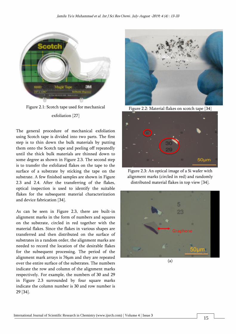
The general procedure of mechanical exfoliation
using Scotch tape is divided into two parts. The first
step is to thin down the bulk materials by putting
them onto the Scotch tape and peeling off repeatedly
until the thick bulk materials are thinned down to
some degree as shown in Figure 2.3. The second step
is to transfer the exfoliated flakes on the tape to the
surface of a substrate by sticking the tape on the
substrate. A few finished samples are shown in Figure
2.3 and 2.4. After the transferring of the flakes,
optical inspection is used to identify the suitable
flakes for the subsequent material characterization
and device fabrication [34].
As can be seen in Figure 2.3, there are built-in
alignment marks in the form of numbers and squares
on the substrate, circled in red together with the
material flakes. Since the flakes in various shapes are
transferred and then distributed on the surface of
substrates in a random order, the alignment marks are
needed to record the location of the desirable flakes
for the subsequent processing. The period of the
alignment mark arrays is 76μm and they are repeated
over the entire surface of the substrates. The numbers
indicate the row and column of the alignment marks
respectively. For example, the numbers of 30 and 29
in Figure 2.3 surrounded by four square marks
indicate the column number is 30 and row number is
29 [34].
Figure 2.2: Material flakes on scotch tape [34]
Figure 2.3: An optical image of a Si wafer with
alignment marks (circled in red) and randomly
distributed material flakes in top view [34].
(a)
International Journal of Scientific Research in Chemistry (www.ijsrch.com) | Volume 4 | Issue 3
Jamilu Ya'u Muhammad et al. Int J Sci Res Chemi. July-August -2019; 4 (4) : 13-33
16
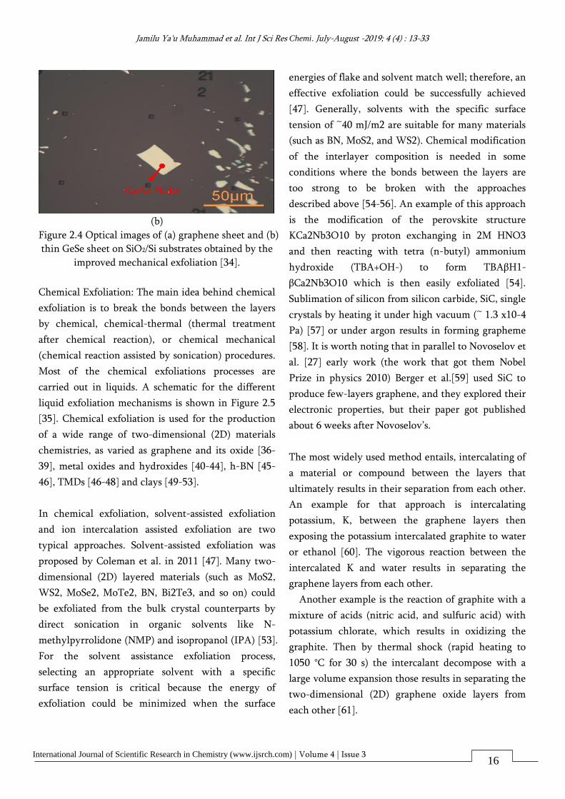
(b)
Figure 2.4 Optical images of (a) graphene sheet and (b)
thin GeSe sheet on SiO2/Si substrates obtained by the
improved mechanical exfoliation [34].
Chemical Exfoliation: The main idea behind chemical
exfoliation is to break the bonds between the layers
by chemical, chemical-thermal (thermal treatment
after chemical reaction), or chemical mechanical
(chemical reaction assisted by sonication) procedures.
Most of the chemical exfoliations processes are
carried out in liquids. A schematic for the different
liquid exfoliation mechanisms is shown in Figure 2.5
[35]. Chemical exfoliation is used for the production
of a wide range of two-dimensional (2D) materials
chemistries, as varied as graphene and its oxide [36-
39], metal oxides and hydroxides [40-44], h-BN [45-
46], TMDs [46-48] and clays [49-53].
In chemical exfoliation, solvent-assisted exfoliation
and ion intercalation assisted exfoliation are two
typical approaches. Solvent-assisted exfoliation was
proposed by Coleman et al. in 2011 [47]. Many two-
dimensional (2D) layered materials (such as MoS2,
WS2, MoSe2, MoTe2, BN, Bi2Te3, and so on) could
be exfoliated from the bulk crystal counterparts by
direct sonication in organic solvents like N-
methylpyrrolidone (NMP) and isopropanol (IPA) [53].
For the solvent assistance exfoliation process,
selecting an appropriate solvent with a specific
surface tension is critical because the energy of
exfoliation could be minimized when the surface
energies of flake and solvent match well; therefore, an
effective exfoliation could be successfully achieved
[47]. Generally, solvents with the specific surface
tension of ~40 mJ/m2 are suitable for many materials
(such as BN, MoS2, and WS2). Chemical modification
of the interlayer composition is needed in some
conditions where the bonds between the layers are
too strong to be broken with the approaches
described above [54-56]. An example of this approach
is the modification of the perovskite structure
KCa2Nb3O10 by proton exchanging in 2M HNO3
and then reacting with tetra (n-butyl) ammonium
hydroxide (TBA+OH-) to form TBAβH1-
βCa2Nb3O10 which is then easily exfoliated [54].
Sublimation of silicon from silicon carbide, SiC, single
crystals by heating it under high vacuum (~ 1.3 x10⁻⁴
Pa) [57] or under argon results in forming grapheme
[58]. It is worth noting that in parallel to Novoselov et
al. [27] early work (the work that got them Nobel
Prize in physics 2010) Berger et al.[59] used SiC to
produce few-layers graphene, and they explored their
electronic properties, but their paper got published
about 6 weeks after Novoselov’s.
The most widely used method entails, intercalating of
a material or compound between the layers that
ultimately results in their separation from each other.
An example for that approach is intercalating
potassium, K, between the graphene layers then
exposing the potassium intercalated graphite to water
or ethanol [60]. The vigorous reaction between the
intercalated K and water results in separating the
graphene layers from each other.
Another example is the reaction of graphite with a
mixture of acids (nitric acid, and sulfuric acid) with
potassium chlorate, which results in oxidizing the
graphite. Then by thermal shock (rapid heating to
1050 °C for 30 s) the intercalant decompose with a
large volume expansion those results in separating the
two-dimensional (2D) graphene oxide layers from
each other [61].
International Journal of Scientific Research in Chemistry (www.ijsrch.com) | Volume 4 | Issue 3
Jamilu Ya'u Muhammad et al. Int J Sci Res Chemi. July-August -2019; 4 (4) : 13-33
17
Sonication assisted exfoliation can also be used instead
of thermal shock to exfoliate the intercalated
graphene oxide layers [62]. Exfoliation of TMDs can
be carried out by sonicating their powders in different
solvents such as N-methyl-pyrrolidone or isopropanol
[46]. Similarly, graphene sheets can be exfoliated by
sonication in water with additives of surfactants [63].
As shown in Figure 2.5c, using the right solvent is
very important to avoid restacking and re-
agglomeration [46].
Figure 2.5: Schematic for the different liquid
exfoliation mechanisms (a) Intercalation followed by
agitation, (b) chemical modification by exchanging
the compound that is between the layers by other
intercalants followed by agitation, and, (c) sonication,
if carried out in the right solvent, the sonicated layers
will stay in suspension for a long time, if not the
layers will restack [35].
A. Bottom-up Approach
The main techniques that use a bottom-up
approach to synthesis 2D materials are chemical
vapor deposition, CVD and physical vapor
deposition, PVD.
Chemical Vapor Deposition (CVD): This involves
chemical reactions of gaseous reactants on a
heated substrate surface [64-65]. The CVD
approach has been used successfully in
synthesizing 1T-VS2 [66, 67], 1T-VSe2 [68, 69],
2H-NbS2 [70], 3R-NbS2 [70], 2H-NbSe2 [71], 1T-
TaS2 [72, 73], 1T-TiSe2 [74], and so on.
Contamination-free and high crystalline quality
samples with potential for scaling-up are the
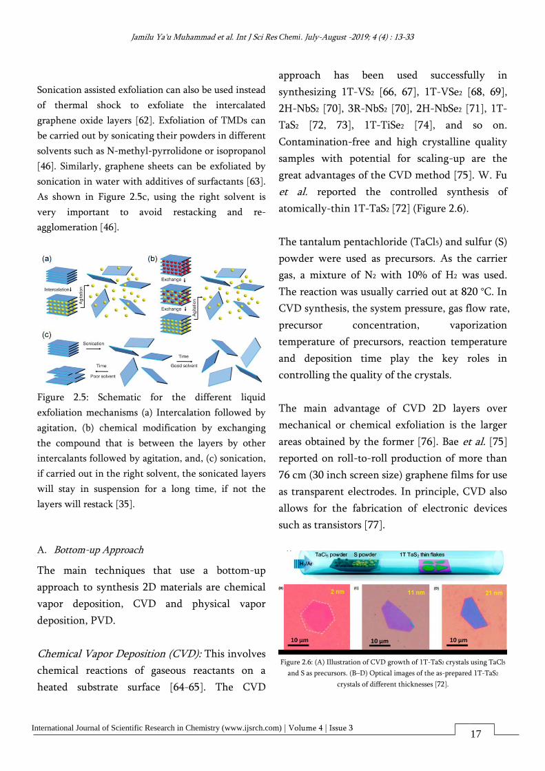
great advantages of the CVD method [75]. W. Fu
et al. reported the controlled synthesis of
atomically-thin 1T-TaS2 [72] (Figure 2.6).
The tantalum pentachloride (TaCl5) and sulfur (S)
powder were used as precursors. As the carrier
gas, a mixture of N2 with 10% of H2 was used.
The reaction was usually carried out at 820 °C. In
CVD synthesis, the system pressure, gas flow rate,
precursor concentration, vaporization
temperature of precursors, reaction temperature
and deposition time play the key roles in
controlling the quality of the crystals.
The main advantage of CVD 2D layers over
mechanical or chemical exfoliation is the larger
areas obtained by the former [76]. Bae et al. [75]
reported on roll-to-roll production of more than
76 cm (30 inch screen size) graphene films for use
as transparent electrodes. In principle, CVD also
allows for the fabrication of electronic devices
such as transistors [77].
Figure 2.6: (A) Illustration of CVD growth of 1T-TaS2 crystals using TaCl5
and S as precursors. (B–D) Optical images of the as-prepared 1T-TaS2
crystals of different thicknesses [72].
International Journal of Scientific Research in Chemistry (www.ijsrch.com) | Volume 4 | Issue 3
Jamilu Ya'u Muhammad et al. Int J Sci Res Chemi. July-August -2019; 4 (4) : 13-33
18
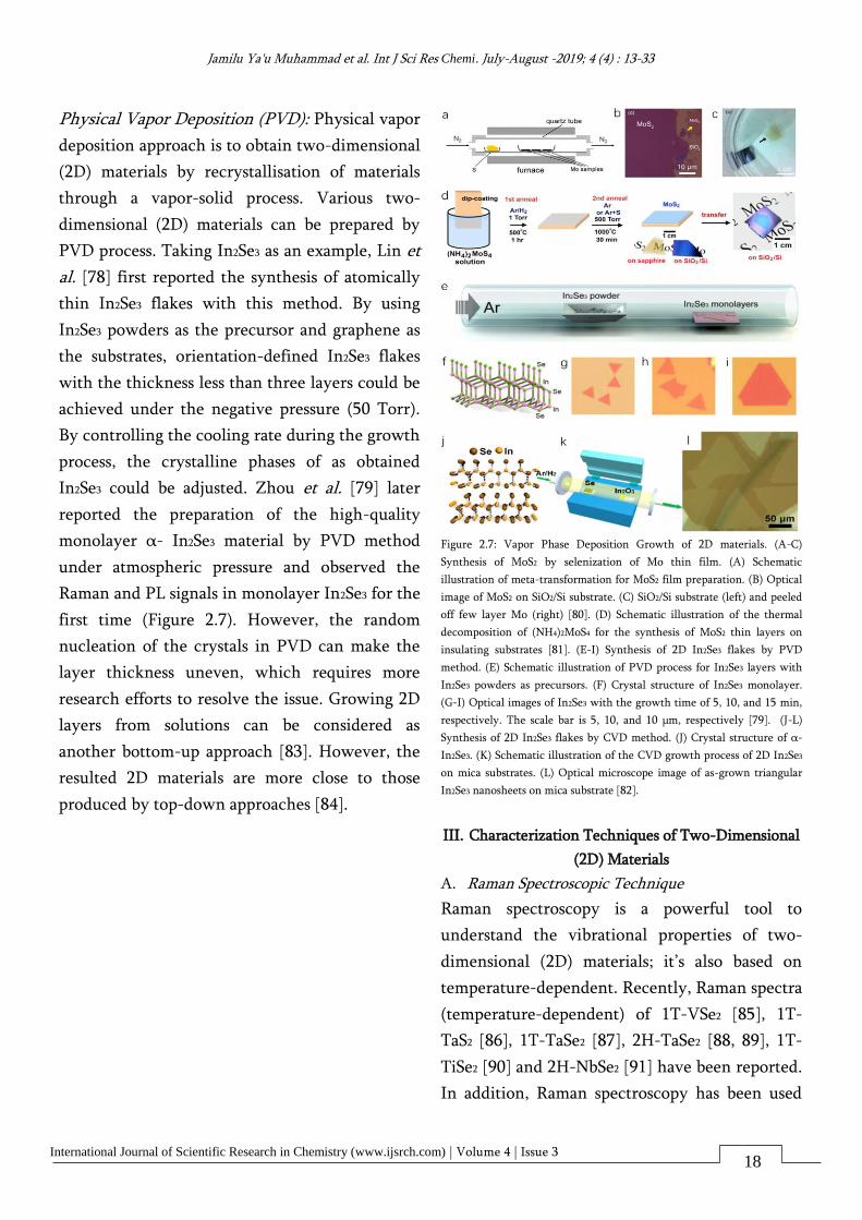
Physical Vapor Deposition (PVD): Physical vapor
deposition approach is to obtain two-dimensional
(2D) materials by recrystallisation of materials
through a vapor-solid process. Various two-
dimensional (2D) materials can be prepared by
PVD process. Taking In2Se3 as an example, Lin et
al. [78] first reported the synthesis of atomically
thin In2Se3 flakes with this method. By using
In2Se3 powders as the precursor and graphene as
the substrates, orientation-defined In2Se3 flakes
with the thickness less than three layers could be
achieved under the negative pressure (50 Torr).
By controlling the cooling rate during the growth
process, the crystalline phases of as obtained
In2Se3 could be adjusted. Zhou et al. [79] later
reported the preparation of the high-quality
monolayer α- In2Se3 material by PVD method
under atmospheric pressure and observed the
Raman and PL signals in monolayer In2Se3 for the
first time (Figure 2.7). However, the random
nucleation of the crystals in PVD can make the
layer thickness uneven, which requires more
research efforts to resolve the issue. Growing 2D
layers from solutions can be considered as
another bottom-up approach [83]. However, the
resulted 2D materials are more close to those
produced by top-down approaches [84].
Figure 2.7: Vapor Phase Deposition Growth of 2D materials. (A-C)
Synthesis of MoS2 by selenization of Mo thin film. (A) Schematic
illustration of meta-transformation for MoS2 film preparation. (B) Optical
image of MoS2 on SiO2/Si substrate. (C) SiO2/Si substrate (left) and peeled
off few layer Mo (right) [80]. (D) Schematic illustration of the thermal
decomposition of (NH4)2MoS4 for the synthesis of MoS2 thin layers on
insulating substrates [81]. (E-I) Synthesis of 2D In2Se3 flakes by PVD
method. (E) Schematic illustration of PVD process for In2Se3 layers with
In2Se3 powders as precursors. (F) Crystal structure of In2Se3 monolayer.
(G-I) Optical images of In2Se3 with the growth time of 5, 10, and 15 min,
respectively. The scale bar is 5, 10, and 10 μm, respectively [79]. (J-L)
Synthesis of 2D In2Se3 flakes by CVD method. (J) Crystal structure of α-
In2Se3. (K) Schematic illustration of the CVD growth process of 2D In2Se3
on mica substrates. (L) Optical microscope image of as-grown triangular
In2Se3 nanosheets on mica substrate [82].
III. Characterization Techniques of Two-Dimensional
(2D) Materials
A. Raman Spectroscopic Technique
Raman spectroscopy is a powerful tool to
understand the vibrational properties of two-
dimensional (2D) materials; it’s also based on
temperature-dependent. Recently, Raman spectra
(temperature-dependent) of 1T-VSe2 [85], 1T-
TaS2 [86], 1T-TaSe2 [87], 2H-TaSe2 [88, 89], 1T-
TiSe2 [90] and 2H-NbSe2 [91] have been reported.
In addition, Raman spectroscopy has been used
International Journal of Scientific Research in Chemistry (www.ijsrch.com) | Volume 4 | Issue 3
Jamilu Ya'u Muhammad et al. Int J Sci Res Chemi. July-August -2019; 4 (4) : 13-33
19
vastly to investigate stacking order [92, 93],
number of layers [94], molecular doping [95],
edge orientations [96, 97], strain effects [98, 99]
and other properties of two-dimensional (2D)
materials. Raman spectroscopy provides a quick,
convenient, nondestructive and noninvasive
method for characterizing the 2D materials with
high selectively for the interior layers [100-102,
104]. Measurements can be made at room
temperature and at ambient pressure without
complicated sample preparation processes.
Raman scattering involves the inelastic scattering
of the incident light in a material, where the
energy of the scattered light either decreases by
exciting an elementary excitation of the solid
material (i.e. a phonon) or increases by absorbing
a phonon.
More accurately, Raman spectroscopy can also be
used to determine the number of layers of 2D
TMDs. Since the Raman spectrum provides
vibrational information of the phonon structure
specific to molecules which have unique Raman
peaks in Raman spectra, it is used as a fingerprint
to identify the molecule and an effective and
quick technique to differentiate one from others.
Two Raman peaks are observed in various
thicknesses of MoS2. One corresponds to in-plane
E12g mode, located at 384 cm-1 and the other out-
plane A1g mode, located at 408 cm-1. And the
exact positions of E12g mode and A1g mode are
functions of MoS2 film thickness. As the MoS2
film thickness increases, E12g mode decreases but
A1g mode shifts in an opposite direction, which
originates from the effective restoring forces and
long-range Coulomb interactions [103]. The
noticeable shifts of E12g mode and A1g mode make
the Raman spectra an excellent indicator of
thickness in MoS2 film, which also applies to
other 2D TMDs, such as WS2, MoSe2, etc.
Raman spectra give the intensity of the scattered
light as a function of the energy shift from the
incident light (Raman shift). The typical accuracy
of measurements of Raman spectra is 1 cm-1 (~0.1
meV) which is sufficient for measuring the
interlayer interaction (several meV) of TMDs.
Raman spectroscopy has been widely used and
has become a standard characterization
technique for TMDs, graphene and other atomic
layer materials [101].
There are several advantages of using Raman
spectroscopy for the characterization of low
dimensional materials, including 2D TMDs [104,
105]. One reason is that the electronic density of
states (DOS) has a so-called van Hove singularity
[107], which leads to a strong Raman feature
when the photon energy is matched to the van
Hove singularity of the DOS for each layer.
The second advantage is that more specific
selection rules predicted from the group theory
applicable to the particular optical transition can
be applied to many TMD layered materials with
lower symmetry compared to graphene. In this
way, differences in symmetry distinguish the
spectral features of a particular TMD layer from
another.
In addition, in the optical transitions involved in
the Raman process, the optical dipole selection
rule restricts the possible electronic transitions
and the possible Raman-active phonon modes,
which could be sensitive to the number of atomic
International Journal of Scientific Research in Chemistry (www.ijsrch.com) | Volume 4 | Issue 3
Jamilu Ya'u Muhammad et al. Int J Sci Res Chemi. July-August -2019; 4 (4) : 13-33
20
layers and to the laser polarization direction [106,
107].
B. Temperature-Dependent Resistivity and Magnetic
Susceptibility
As the temperature changes, an unusual response
in resistivity and magnetic susceptibility has been
observed in two-dimensional (2D) material such
as 1T-VS2 [116], 1T-VSe2 [73, 109, 110], 1T-TaS2
[107, 112, 113] and 1T-TaSe2 [114] which is also
an indication of two-dimensional CDW
transition. The thickness plays an important role
in the CDW phase transition of 2D CDW
materials.
The thickness dependence of the NC-CDW to C-
CDW phase transition temperature in 1T-TaS2
thin flakes had been reported by M. Yoshida et al.
for the first time [115]. The dimensionality effect
on CDW states in 1T-TaS2 was analyzed by
investigating pristine thin flakes by changing the
thicknesses up to 2 nm approximately [116, 117].
It was demonstrated that both C-CDW/NC-CDW
and NC-CDW/IC-CDW phase transitions are
dynamically regulated for varying the sample
thickness.
In contrast to 1T-TaS2 and 1T-VSe2, it is also
reported that the CDW phase transition
temperature can increase in the thinner materials.
For instance, the liquid-exfoliated 4–8 layer-
thick 1T-VSe2 sample shows the CDW phase
transition temperature at 135 K, whereas the
bulk sample shows it at 107 K [117]. A similar
phenomenon has been observed from
mechanically-exfoliated TiSe2 samples, where the
transition temperature increases from 200–240 K,
while thinning the thickness from the bulk to a
few nanometers [96]. Moreover, X. Xi et al.
reported the strongly enhanced CDW order in
atomically-thin NbSe2 TCDW > 100 K for the
exfoliated monolayer sample [118], while M.
Ugeda et al. observed slightly weakened CDW
order (TCDW approximately 25 K) in the single
layer NbSe2 grown on graphene by the MBE
method [119]. These dissimilarities of the
transition temperature still are not well
understood. The sample quality, substrates and
the fabricated device status could play crucial
roles in CDW phase transitions.
C. X-Ray Diffraction Technique
X-ray Diffraction (XRD) both small-angle X-ray
scattering (SAXS) and wide-angle XRD can
supply information about the unit cell structure
and constituents, the sheet thickness and lateral
dimensions, and the arrangement of restacked
nanosheets. SAXS provides information about
inter-nanosheet stacking since these peaks occur
at lower angles [120]. By simulating the SAXS
pattern, the stacking direction, sheet thickness,
and distance between the sheets (from ligands or
absorbed molecules) can be determined. For
instance, patterns of wet colloidal aggregates of
nanosheets and dried aggregates of nanosheets
will display different XRD patterns: layer-to-
layer registry can be disturbed for wet colloidal
aggregates, while in-plane lattice planes are
maintained, suggesting isolated nanosheets [121,
122]. For dried nanosheets, the presence of low-
angle basal reflections in the pattern indicates an
ordered arrangement of restacked nanosheets
along the stacking axis, and likewise, the absence
of intense basal reflections indicates random
orientations for aggregated nanosheets [121]. The
orientation of films on substrates favors the
alignment of the thin axis. Broadening signatures
of specific peaks under this orientation can
International Journal of Scientific Research in Chemistry (www.ijsrch.com) | Volume 4 | Issue 3
Jamilu Ya'u Muhammad et al. Int J Sci Res Chemi. July-August -2019; 4 (4) : 13-33
21
indicate the thin axis [122]. To gain more insight,
the nanosheet XRD pattern can be modeled by
the structure factor, the Lorentz polarization
factor, the Laue interference function, and the
temperature factor [123]. Structure factors for
single and multiple layers can be calculated
assuming atomic positions, unit cell structure,
and orientation to a substrate [124]. Results of
this modeling can help determine the
fundamental units of the nanosheets (e.g., atomic
make up of termination layers), the spacing
between sheets, and if the nanosheets are
restacked. In plane XRD can be used successfully
to observe ‘hk’ reflections (if l is the thickness
axis) of the nanosheets' 2D unit cell [125]. This is
a useful method to observe missing peaks from
the naturally textured orientation of nanosheets
on a substrate. Unit cell parameters can be
extracted from refinements of these data and
compared to bulk values.
D. Scanning Tunneling Microscopic Technique
Scanning Tunneling Microscopy (STM) is a
probe-based technique that can measure the
electronic and topographic structure of single-
atom-thick materials and can manipulate single
atoms at specific points in order to build and
characterize nanostructures that are well isolated
from the substrate [126].
Atomic arrangement in 2D materials regulates
the electronic structures. Scanning Tunneling
Microscopy (STM) imaging and scanning
tunneling spectroscopy (STS) measurement are
direct ways to reveal the atomic structure and the
energy gap of 2D materials. M. M. Ugeda et al.
[119] reported Scanning Tunneling Microscopy
(STM) measurements on ultrathin film of 2H-
NbSe2. A three by three CDW structure in NbSe2
has been observed. Superconductivity also
remains in the 2D limit, but the transition
temperature is lowered to 1.9 K (7.2 K for the
bulk material).
Another examples include Scanning Tunneling
Microscopy (STM) studies of the unusual
cyclotron quantization in graphene [127, 128] as
well as characterization of MoS2 nanoislands [129]
and BN [130] Recent focus has shifted toward
studies of adsorbates and defects, including metal
adatoms on graphene [131, 132] and h-BN [133,
134] and molecules on MoS2 [135].
Other characterization techniques are Scanning
Transmission Electron Microscopy (STEM) [136],
Transmission Electron Microscopy (TEM) [137],
Fluorescence Quenching Microscopy (FQM)
[126], Scanning Electron Microscopy (SEM) [84],
and so on.
1. Potential Applications of Two-Dimension (2D)
Materials
Two-dimensional materials are newly developed
materials with better performance evaluations
and widely applications. This section will gives
some of potential applications of two-
dimensional materials.
E. Catalytic Activity
Ma et al. [138] found that Al-doped graphene-
like Zinc Oxide (g-ZnO) mono-layers in which
Al atoms substitute host Zn atoms show good
catalytic activity for CO oxidation via the Eley–
Rideal mechanism with a two-step route. In this
mechanism, the first CO molecule directly
interacts with the pre-adsorbed O2 molecule,
forming a carbonate-like CO3 complex as an
International Journal of Scientific Research in Chemistry (www.ijsrch.com) | Volume 4 | Issue 3
Jamilu Ya'u Muhammad et al. Int J Sci Res Chemi. July-August -2019; 4 (4) : 13-33
22
intermediate state. This process is exothermic by
3.93 eV and the reaction requires only a small
barrier of 0.006 eV to be overcome. The second
CO molecule initially adsorbed on top of one Zn
atom near the doped Al atom then approaches
the CO3 complex to form two CO2 molecules
with an energy barrier of 0.79 eV. Two CO2
molecules are produced with adsorption energy
of 0.46 eV with respect to two free CO2
molecules in the gas phase. Since the energy
released in this step (0.79 eV) can easily
surmount the adsorption energy, these two CO2
molecules can be released rather easily from the
g-ZnO sheet. The reaction proceeds rapidly at
low temperature, suggesting that Al-doped g-
ZnO mono-layers could be an efficient catalyst
for CO oxidation at low temperature.
A. Absorption of Oxide of Carbon
Rao et al. [139] investigated the interaction of
CO2 with pristine, defective and non-metal-
doped graphene-like Zinc Oxide (g-ZnO) mono-
layers in terms of their efficiency to capture CO2
and hence their potential for cleaning our
atmosphere and purifying fuel engine emissions.
The calculated results show that a CO2 molecule
favors adsorption on the top of an O location and
favors a horizontal alignment with respect to the
pristine g-ZnO mono-layer (ML). The adsorption
energy of the CO2 molecule on a g-ZnO mono-
layer is found to be -0.20 eV, indicating
physisorption with a CO2–gZnO distance of 2.92
Å. The CO2 adsorption on defective as well as
non-metal (B, C, N), substitutionally doped g-
ZnO mono-layers was also investigated. The
adsorption of CO2 at oxygen and zinc vacancies
was explored in the study on defective g-ZnO.
The adsorption energy of CO2 increases to -1.77
eV, -1.33 eV and -0.80 eV with adsorption
distances of 1.53 Å, 1.44 Å and 1.41 Å for B, C
and N atoms, respectively. This indicates a
chemisorption mechanism with a large binding
energy and a short adsorption distance and stands
in contrast with physisorption on pristine g-ZnO.
In another research, Zhang et al. [140] have
reported that doped g-ZnO exhibits strong
chemisorption of the CO molecule by forming A-
CO (where A=B, N or C dopants) in contrast to
weak physisorption on pristine g-ZnO. The
adsorbed CO slightly pulls the A atom out of the
sheet plane, viz. the A site is transformed from
sp2 hybridization to a more sp3-like hybridization.
Total charge density calculations show that large
charge transfer occurs between the doped g-ZnO
and a CO molecule, while little charge is
transferred between pristine g-ZnO and a CO
molecule. Moreover, the shorter bond lengths of
A–CO (1.43 Å, 1.24 Å, 1.32 Å for B, N and C,
respectively, as compared to pristine g-ZnO, 2.32
Å) and a higher binding energy (-4.05, -2.77, -
5.65 eV for B, N and C, respectively, as compared
to pristine g-ZnO -0.35 eV) clearly indicate that a
chemical bond can form during the adsorption
process.
B. Energy Storage and Harvesting
The energy harvesting cells based on 2D
piezoelectric materials are crucial for future
wireless nanosystems without power supply,
such as environmental monitors, implantable
medical sensors, and personal electronics [141].
In 2014, Wu et al. [142] pioneered a monolayer
MoS2 as prototype nanogenerator for scavenging
the mechanical energy. As for this nanogenerator,
it will generate a peak voltage or current signal
only during the moment of stretching and
International Journal of Scientific Research in Chemistry (www.ijsrch.com) | Volume 4 | Issue 3
Jamilu Ya'u Muhammad et al. Int J Sci Res Chemi. July-August -2019; 4 (4) : 13-33
23
releasing. With the increasing tensile strain, both
the peak voltage and current increase.
Furthermore, this type of device can still
maintain a stable output even after three hours of
fatigue test, demonstrating its excellent
performance for harvesting various tiny
mechanical vibration energies. Enlightened by
this work, Lee et al. [143] developed a monolayer
WSe2 piezoelectric nanogenerator, which gives a
peak voltage of 45 mV under a strain of 0.39 %.
In their work, to enhance the piezoelectric
outputs, CVD synthesized monolayer WSe2
samples have been successfully transferred to the
top of another one to form a special-orientated
artificial bilayer (AA stacking), which could
retain the piezoelectric effect, unlike its natural
or pristine form. The piezoelectric coefficient for
artificial bilayer can be about two times larger
than that of the monolayer flakes.
Phosphorene has been considered for other
electrochemical energy storage applications, such
as all solid- state supercapacitors [144] and
Sodium ion batteries (NaIBs), [145] which are
considered safer than LIBs and use more
abundant Sodium ions. The promise of using
phosphorene for NaIB anode materials comes
from the fact that, unlike the traditional, carbon-
based anode materials for LIBs, it can
accommodate Na ions, which are significantly
larger than Li ions (2.04 vs. 1.52 Å). Because of
this, BP with its larger interlayer channel size
(3.08 vs. 1.86 Å for graphite) is a highly
promising NaIB anode material with a theoretical
specific capacity of ~2600 mAh g−1, which dwarfs
that of any other present materials.
C. Electronics and Sensing Devices
Generally, two-dimensional (2D) materials could
be an ideal choice for future flexible electronics.
They have excellent mechanical properties [146,
147], can be compatible with flexible device
fabrication, and unlike CNTs [148, 149] do not
require any sorting process [150]. At the same
time, the mobility of 2DMs, when grown over
large areas by CVD, can be larger than some of
the organic semiconductors [151], thus enabling
higher frequency at low power. For transparent
conductors, graphene high conductivity and low
broadband absorption makes it a promising
flexible replacement for the current leading
material, indium tin oxide, which is inflexible
and increasingly expensive. The large variety of
two-dimensional (2D) materials provides a wide
selection to choose for device optimization.
Optoelectronic devices (photodetectors, solar
cells and LEDs etc.) are electric devices that can
generate, detect, and interact with light. Due to a
large area/volume ratio, strong light–matter
interaction and novel electrical properties,
optoelectronic devices based on two-dimensional
(2D) materials have attracted much interest since
the beginning.
The direct band gaps of monolayer TMDs make
them attractive as light-absorbing materials in
alternative thin-film solar cells, including flexible
photovoltaics that could coat buildings and
curved structures. The first trial was on MoS2
[152]. This was inspired by the finding that MoS2
has a direct band gap of about 1.8 eV when its
thickness is reduced to a single layer. In 2013,
Lopez-Sanchez et al. conducted a landmark
research [153]. They reduced charged impurities
scattering and contact resistance by the careful
treatment on a dielectric layer and an annealing
process. After these processes, an impressive high
International Journal of Scientific Research in Chemistry (www.ijsrch.com) | Volume 4 | Issue 3
Jamilu Ya'u Muhammad et al. Int J Sci Res Chemi. July-August -2019; 4 (4) : 13-33
24
responsivity of 880 AW-1 was achieved.
Stimulated by the pioneering works on MoS2,
photo-detectors based on other TMDs, like
MoSe2, WS2 and WSe2, have attracted growing
attention in recent years [154–156]. In addition,
combining different 2-D materials together to
form heterostructures may be a possible solution
[157, 158].
D. CO2 reduction
Li et al. [159] reported amorphous MoS2 on a
polyethylenimine-modified reduced graphene
oxide substrate as an effective catalyst for
electrocatalytic CO2 reduction. The catalyst is
capable of producing CO at an over potential as
low as 140 mV and reaches a maximum Faradaic
efficiency (FE) of 85.1% at an over potential of
540 mV. Another interesting point is that at an
over potential of 290 mV with respect to the
formation of CO, it catalyses the formation of
syngas with high stability, which could be readily
utilized in the current Fischer-Tropsch process
and produce liquid fuels, such as ethanol and
methanol. Their detailed mechanism
investigation indicated that the efficiency and
selectivity towards CO2 reduction rather than
hydrogen evolution at the optimal applied
potential were attributed to the synergetic effect
of MoS2 and PEI:
a) The intrinsic properties of MoS2 that it can
selectively bind the intermediate during the
CO2 reduction reaction path is the principal
factor contributing the CO2 reduction and
b) PEI, an amine containing polymer with
outstanding CO2 adsorption capacity, can
stabilize the intermediate and thus lower
the energy barrier by hydrogen bond
interaction.
Recently, Norskov et al. demonstrated
theoretically that MoS2 or MoSe2 could possibly
be electrocatalysts for CO2 reduction by DFT
calculation [160, 161]. Their results indicate the
edge site of MoS2 or MoSe2 is active for
electrochemical CO2 reduction due to the
different scaling relationships of adsorption
energies between key reaction intermediates
(*CO and *COOH) on the edges of MoS2 or MoSe2
compared to transition metals. Experimental
results of MoS2 as electrocatalyst for CO2
reduction were firstly reported by Asadi et al.
[162]. They uncovered that MoS2 showed
superior CO2 reduction performance compared
with the noble metals with a high current
density and low over potential (54 mV) in an
ionic liquid. They also utilized DFT calculations
to reveal the catalytic activity mainly arises from
the molybdenum-terminated edges of MoS2 due
to their metallic character and a high d-electron
density. The experimental result that vertically
aligned MoS2 showed an enhanced performance
compared to bulk MoS2 crystal supported their
calculations.
IV. Conclusion and Future Works
In conclusion, the synthesis processes,
characterization techniques and potential
applications of two-dimensional materials with
consideration of elecrocatalysis have been
discussed extensively.
Though great progress has been made, it is still
far from the wide application of 2D
electrocatalysis. There are still many challenges
like the low yield/cost efficiency, degradation,
International Journal of Scientific Research in Chemistry (www.ijsrch.com) | Volume 4 | Issue 3
Jamilu Ya'u Muhammad et al. Int J Sci Res Chemi. July-August -2019; 4 (4) : 13-33
25
kinetics of charge transfer and trap, and recycling.
The recycling problem may be resolved by
designing suitable devices or tuning the magnetic
properties, but the efficiency and robustness can
only count on the development of more
advanced materials.
The 2D material family offers a new class of
materials characterized by strong covalent bonds
in-plane but only very weak Van der Waal’s
coupling between the layers, leading to a material
system with almost ideally self-passivated
structures.
The most promising applications of 2D materials
must be developed based on the unique
properties of this material system that are not
often found in other materials. 2D materials offer
three key properties that are particularly
attractive for future applications: the flexibility
and transparency, the ease for heterogeneous
integration without lattice mismatch problem,
and extraordinary sensing capability due to high
surface-to-volume ratio and high mobility.
The first area is to develop 2D materials for GHz
frequency ubiquitous electronics applications.
A second promising application of 2D materials
lies in their outstanding optical properties.
Optoelectronics devices, such as photodetectors,
LEDs and even lasers, based on 2D materials can
be envisioned to emerge where they can be
placed on to arbitrary surfaces including flexible
and transparent ones. New opportunities can
arise in developing THz and infrared sensors
based on graphene either based on conventional
device structure or novel plasmonic devices. Low
cost solar cells to be placed on any type of
substrates can also be developed where many
potential applications exist, for example as the
energy harvesting units in self-powered sensors
or sensor networks.
2D materials like graphene are very attractive
bio-compatible options of flexible and
semitransparent electrodes for interfacing with
the brain neurons. 2D materials can also be used
to build low-cost biosensors with many potential
applications, such as glucose detection, moisture
sensing, and body temperature monitoring.
V. REFERENCES
1. Fengwang Li and Mianqi Xue (2016). Two-
Dimensional Transition Metal Dichalcogenides
for Electrocatalytic Energy Conversion
Applications, retrieved from
http://dx.doi.org/10.5772/63947
2. Novoselov KS, Geim AK, Morozov S, Jiang D,
Zhang Y, Dubonos Sa (2004). Electric field
effect in atomically thin carbon films. Science;
306:666-669.
3. Mueller, T., Xia, F. & Avouris, P. (2010).
Graphene photodetectors for high-speed optical
communications. Nat. Photon. 4, 297-301.
4. Liu, Y. (2011). Plasmon resonance enhanced
multicolour photodetection by graphene. Nat.
Commun. 2, 579.
5. Applied Graphene Materials plc: Graphene
dispersions Retrieved from
http://www.appliedgraphenematerials.com
6. Hu Guohua, Kang Joohoon, Ng Leonard W. T,
Zhu Xiaoxi, Howe Richard C. T., John
Christopher G., Hersam Mark C., Hasan
Tawfique (2018). Functional inks and printing
of two-dimensional materials. Chemical Society
Reviews. 47(9), pp: 3265-3300.
7. Kerativitayanan P., Carrow J. K., Gaharwar A.
K., (2015). Nanomaterials for Engineering Stem
International Journal of Scientific Research in Chemistry (www.ijsrch.com) | Volume 4 | Issue 3
Jamilu Ya'u Muhammad et al. Int J Sci Res Chemi. July-August -2019; 4 (4) : 13-33
26
Cell Responses. Advanced Healthcare Materials.
4(11), pp: 1600-1627.
8. Gaharwar A. K., Peppas N. A., Khademhosseini
A., (2014). Nanocomposite hydrogels for
biomedical applications. Biotechnology and
Bioengineering. 111(3), pp: 441-453.
9. Chhowalla M., Shin H. S., Eda G., Li L. J., Loh
K. P., Zhang H. (2013). The chemistry of two-
dimensional layered transition metal
dichalcogenide nanosheets. Nature Chemistry;
5:263-275.
10. Das S., Robinson J. A., Dubey M., Terrones H.,
Terrones M. (2015). Beyond graphene: progress
in novel two-dimensional materials and van der
Waals solids. Annual Review of Materials
Research; 45:1-27.
11. Sun Y, Gao S, Lei F, Xie Y. (2015). Atomically-
thin two-dimensional sheets for understanding
active sites in catalysis. Chemical Society
Reviews; 44:623-636.
12. Wang Z, Zhu W, Qiu Y, Yi X, von dem Bussche
A, Kane A, et al. (2016). Biological and
environmental interactions of emerging two-
dimensional nanomaterials. Chemical Society
Reviews; 45:1750-1780.
13. Zhang X & Xie Y. (2013). Recent advances in
free-standing two-dimensional crystals with
atomic thickness: design, assembly and transfer
strategies. Chemical Society Reviews; 42:8187-
8199.
14. Luo B, Liu G, Wang L. (2016). Recent advances
in 2D materials for photocatalysis. Nanoscale;
8:6904-6920. DOI: 10.1039/c6nr00546b.
15. Garcia J. C., De Lima D. B., Assali L. V. C., Justo
J. F., (1324). Group IV grapheme and graphene-
like nanosheets. Journal of Physical Chemistry
C. 115(27), pp: 13242-13246.
16. Lei Yang, Ping Liu, Jing Li and Bin Xiang
(2017). Two-Dimensional Material
Molybdenum Disulfides as Electrocatalysts for
Hydrogen Evolution. Catalysts, 7, 285; pp 1-18,
doi:10.3390/catal7100285. Retrieved from
www.mdpi.com/journal/catalysts
17. Valenti G., Boni A., Melchionna M., Cargnello
M., Nasi L., Bertoli G., Gorte R. J., Marcaccio
M., Rapino S., Bonchio M., Fornasiero P., Prato
M., Paolucci F. (2016). Co-axial
Heterostructures Integrating
Palladium/Titanium-dioxide with Carbon
Nanotubes for Efficient Electrocatalytic
Hydrogen Evolution. Nature Communications.
7: 13549.
18. Wang Xin (2018).CNTs tuned to provide
electrocatalyst support. Retrieved from
http://www.nanotechweb.org
19. Hong W. T., Risch M., Stoerzinger K. A.,
Grimaud A., Suntivich J., Shao-Horn Y. (2015).
Toward the rational design of non-precious
transition metal oxides for oxygen
electrocatalysis. Energy and Environmental
Science; 8, pp:1404-1427.
20. Bonaccorso F., Colombo L., Yu G., Stoller M.,
Tozzini V., Ferrari A. C., (2015). Two-
dimensional (2D) materials. Graphene, related
two-dimensional crystals, and hybrid systems
for energy conversion and storage. Science;
347:1246501.
21. Xie J., & Xie Y. (2015). Transition metal nitrides
for electrocatalytic energy conversion:
opportunities and challenges. Chemistry - A
European Journal; 22, pp: 3588-3598.
22. Zhang G., Liu H., Qu J., Li J. (2016). Two-
dimensional layered MoS2: rational design,
properties and electrochemical applications.
Energy and Environmental Science; 9, pp; 1190-
1209. DOI: 10.1039/c5ee03761a.
23. Mallouk T. E. (2013). Water electrolysis: divide
and conquer. Nature Chemistry; 5, pp: 362-363.
24. Turner J. A. (2004). Sustainable hydrogen
production. Science; 305, pp: 972-974.
25. Norskov J. K., & Christensen C. H. (2006).
Toward efficient hydrogen production at
surfaces. Science; 312, pp: 1322-1323.
26. Novoselov, K. S., Jiang, D., Schedin, F., Booth,
T. J., Khotkevich, V. V., Morozov, S. V., &
Geim, A. K. (2005). Two-dimensional atomic
crystals. Proceeding National Acadamic Science.
USA 102, pp: 10451-10453.
27. K. S. Novoselov, A. K. Geim, S. V. Morozov, D.
Jiang, Y. Zhang, S. V. Dubonos, I. V. Grigorieva,
A. A. Firsov (2004), Science, 306, 666.
28. D. Pacil, J. C. Meyer,. Girit, A. Zettl, (2008).
Applied Physics Letters, 92.

International Journal of Scientific Research in Chemistry (www.ijsrch.com) | Volume 4 | Issue 3
Jamilu Ya'u Muhammad et al. Int J Sci Res Chemi. July-August -2019; 4 (4) : 13-33
27
29. H. Li, G. Lu, Y. Wang, Z. Yin, C. Cong, Q. He,
L. Wang, F. Ding, T. Yu, H. Zhang, (2013).
Small, 9, 1974.
30. K. Kalantar-zadeh, J. Tang, M. Wang, K. L.
Wang, A. Shailos, K. Galatsis, R. Kojima, V.
Strong, A. Lech, W. Wlodarski, R. B. Kaner,
(2010). Nanoscale, 2, 429.
31. S. Balendhran, J. Deng, J. Z. Ou, S. Walia, J.
Scott, J. Tang, K. L. Wang, M. R. Field, S. Russo,
S. Zhuiykov, M. S. Strano, N. Medhekar, S.
Sriram, M. Bhaskaran, K. Kalantar-zadeh,
(2013). Advanced Materials, 25, 109.
32. K. Kalantar-zadeh, A. Vijayaraghavan, M.-H.
Ham, H. Zheng, M. Breedon, M. S. Strano,
(2010). Chemistry of Materials, 22, 5660.
33. Zhengfeng Yang (2017). Electronic Device
Fabrication and Characterization Based on
Two-Dimensional Materials, Master of Science
Thesis at University of Illinois at Urbana-
Champaign.
34. V. Nicolosi, M. Chhowalla, M. G. Kanatzidis, M.
S. Strano, J. N. Coleman, (2013). Science, 340.
35. Y. Hernandez, V. Nicolosi, M. Lotya, F. M.
Blighe, Z. Sun, S. De, I. McGovern, B. Holland,
M. Byrne, Y. K. Gun'Ko, (2008). Nature
Nanotechnology, 3, 563.
36. S. Park, R. S. Ruoff, (2009). Nature
Nanotechnology, 4, 217.
37. S. Stankovich, D. A. Dikin, R. D. Piner, K. A.
Kohlhaas, A. Kleinhammes, Y. Jia, Y. Wu, S. T.
Nguyen, R. S. Ruoff, (2007). Carbon, 45, 1558.
38. G. Eda, G. Fanchini, M. Chhowalla, (2008).
Nature Nanotechnology, 3, 270.
39. R. Ma, & T. Sasaki, (2010). Advanced Materials,
22, 5082.
40. Y. Omomo, T. Sasaki, Wang, M. Watanabe,
(2003). Journal of the American Chemical
Society, 125, 3568.
41. R. Ma, Z. Liu, L. Li, N. Iyi, T. Sasaki, (2006).
Journal of Materials Chemistry, 16, 3809.
42. L. Li, R. Ma, Y. Ebina, N. Iyi, T. Sasaki, (2005).
Chemistry of Materials, 17, 4386.
43. Q. Wang, & D. OHare, (2012). Chemical
Reviews, 112, 4124.
44. Y. Lin, T. V. Williams, J. W. Connell, (2009).
Journal of Physical Chemistry Letters, 1, 277.
45. J. N. Coleman, M. Lotya, A. ONeill, S. D.
Bergin, P. J. King, U. Khan, K. Young, A.
Gaucher, S. De, R. J. Smith, I. V. Shvets, S. K.
Arora, G. Stanton, H. Y. Kim, K. Lee, G. T. Kim,
G. S. Duesberg, T. Hallam, J. J. Boland, J. J.
Wang, J. F. Donegan, J. C. Grunlan, G.
Moriarty, A. Shmeliov, R. J. Nicholls, J. M.
Perkins, E. M. Grieveson, K. Theuwissen, D. W.
McComb, P. D. Nellist, V. Nicolosi, (2011).
Two-dimensional nanosheets produced by
liquid exfoliation of layered materials. Science,
42, 568-571.
46. Z. Zeng, Z. Yin, X. Huang, H. Li, Q. He, G. Lu,
F. Boey, H. Zhang, (2011). Angewandte Chemie
International Edition, 50, 11093.
47. J. Feng, X. Sun, C. Wu, L. Peng, C. Lin, S. Hu, J.
Yang, Y. Xie, (2011). Journal of the American
Chemical Society, 133, 17832.
48. T. Lan, & T. J. Pinnavaia, (1994). Chemistry of
Materials, 6, 2216.
49. J. Ma, Z.-Z. Yu, Q.-X. Zhang, X.-L. Xie, Y.-W.
Two-dimensional nanosheets produced by
liquid exfoliation of layered materials. Science,
42, 568-571.Mai, I. Luck, (2004). Chemistry of
Materials, 16, 757.
50. M. Valkov, M. Rieder, V. Matejka, P. Capkov,
A. Sliva, (2007). Applied Clay Science, 35, 108.
51. J. H. Park, S. C. Jana, (2003). Macromolecules,
36, 2758.
52. Smith, R. J. et al. (2011). Large-scale exfoliation
of inorganic layered compounds in aqueous
surfactant solutions. Advanced Materials, 23,
3944.
53. R. E. Schaak, T. E. Mallouk, (2000). Chemistry
of Materials, 12, 2513.
54. Y.-S. Han, I. Park, J.-H. Choy (2001). Journal of
Materials Chemistry, 11, 1277.
55. M. M. J. Treacy, S. B. Rice, A. J. Jacobson, J. T.
Lewandowski, (1990). Chemistry of Materials,
2, 279.
56. A. J. Van Bommel, J. E. Crombeen, A. Van
Tooren, (1975). Surface Science, 48, 463.
57. K. V. Emtsev, A. Bostwick, K. Horn, J. Jobst, G.
L. Kellogg, L. Ley, J. L. McChesney, T. Ohta, S.
A. Reshanov, J. Rhrl, (2009). Nature Materials,
8, 203.
International Journal of Scientific Research in Chemistry (www.ijsrch.com) | Volume 4 | Issue 3
Jamilu Ya'u Muhammad et al. Int J Sci Res Chemi. July-August -2019; 4 (4) : 13-33
28
58. C. Berger, Z. Song, T. Li, X. Li, A. Y. Ogbazghi,
R. Feng, Z. Dai, A. N. Marchenkov, E. H.
Conrad, P. N. First, W. A. de Heer, (2004).
Journal of Physical Chemistry B, 108, 19912.
59. L. M. Viculis, J. J. Mack, O. M. Mayer, H. T.
Hahn, R. B. Kaner, (2005). Journal of Materials
Chemistry, 15, 974.
60. M. J. McAllister, J.-L. Li, D. H. Adamson, H. C.
Schniepp, A. A. Abdala, J. Liu, M. Herrera-
Alonso, D. L. Milius, R. Car, R. K. Prud'homme,
I. A. Aksay, (2007). Chemistry of Materials, 19,
4396.
61. G. Wang, J. Yang, J. Park, X. Gou, B. Wang, H.
Liu, J. Yao, (2008). Journal of Physical
Chemistry C, 112, 8192.
62. M. Lotya, Y. Hernandez, P. J. King, R. J. Smith,
V. Nicolosi, L. S. Karlsson, F. M. Blighe, S. De,
Z. Wang, I. T. McGovern, G. S. Duesberg, J. N.
Coleman, (2009). Journal of the American
Chemical Society, 131, 3611.
63. Choy, K. L. (2003). Chemical vapour deposition
of coatings. Progressive Material Science. 48,
pp: 57-170.
64. Hou, X. & Choy, K. L. (2006). Processing and
applications of aerosol-assisted chemical vapor
deposition. Chemical Vapor Deposition, 12, pp:
583-596.
65. Yuan, J.; Wu, J.; Hardy, W.J.; Loya, P.; Lou, M.;
Yang, Y.; Najmaei, S.; Jiang, M.; Qin, F.;
Keyshar, K. (2015). Facile synthesis of single
crystal vanadium disulfide nanosheets by
chemical vapor deposition for efficient
hydrogen evolution reaction. Advanced
Materials, 27, pp: 5605-5609.
66. Ji, Q.; Li, C.; Wang, J.; Niu, J.; Gong, Y.; Zhang,
Z.; Fang, Q.; Zhang, Y.; Shi, J.; Liao, L. (2017).
Metallic vanadium disulfide nanosheets as a
platform material for multi-functional electrode
applications. Nano Letters, 17, pp: 4908-4916.
67. Nicolas, D. B.; Christopher, S. B.; Claire, J. C.;
Ivan, P. P.; Prieto, A. G. (2007). Atmospheric
pressure chemical vapour deposition of
vanadium diselenide thin films. App. Surf. Sci.,
253, 6041-6046.
68. Zhang, Z.; Niu, J.; Yang, P.; Gong, Y.; Ji, Q.; Shi,
J.; Fang, Q.; Jiang, S.; Li, H.; Zhou, X. (2017).
Van der waals epitaxial growth of 2D metallic
vanadium diselenide single crystals and their
extra-high electrical conductivity. Advanced
Materials, 1702359.
69. Wang, X.; Lin, J.; Zhu, Y.; Luo, C.; Suenaga, K.;
Cai, C.; Xie, L. (2017). Chemical vapor
deposition of trigonal prismatic NbS2
monolayer and 3R-polytype few-Layers.
Nanoscale, in revision.
70. Wang, H.; Huang, X.; Lin, J.; Cui, J.; Chen, Y.;
Zhu, C.; Liu, F.; Zeng, Q.; Zhou, J.; Yu, P.
(2017). High-quality monolayer superconductor
NbSe2 grown by chemical vapour deposition.
Nature. Communications, 8, 394.
71. Fu,W.; Chen, Y.; Lin, J.;Wang, X.; Zheng, Q.;
Zhou, J.; Zheng, L.;Wang, H.; He, Y.; Fu, Q.
(2016). Controlled synthesis of atomically thin
1T-TaS2 for tunable charge density wave phase
transitions. Chem. Mater., 28, pp: 7613-7618.
72. Jin, G.; Kim, C.; Jo, H.; Kwon, S.H.; Jeong, S. J.;
Lee, H. B. R.; Ahn, J. H. (2017). Vapor phase
synthesis of TaS2 nanocrystals with iodine as
transport agent. Japan Journal of Applied
Physics, 56, 045501.
73. Boscher, N. D.; Carmalt, C. J.; Parkin, I. P.
(2006). Atmospheric pressure CVD of TiSe2
thin films on glass. Chem. Vap. Deposition, 12,
54-58.
74. Bae, S.; Kim, H.; Lee, Y.; Xu, X.; Park, J.S.;
Zheng, Y.; Balakrishnan, J.; Lei, T.; Kim, H. R.;
Song, Y.I. (2010). Roll-to-roll production of 30-
inch graphene films for transparent electrodes.
Nature Nanotechnology, 5, pp: 574-578.
75. A. N. Obraztsov, (2009). Nature
Nanotechnology, 4, 212.
76. M. P. Levendorf, C. S. Ruiz-Vargas, S. Garg, J.
Park, (2009). Nano Letters, 9, 4479.
77. Lin, M. et al. (2013). Controlled growth of
atomically thin In2Se3 flakes by van der Waals
epitaxy. Journal of American Chemical Society.
135, 13274.
78. Zhou, J. et al. (2015). Controlled synthesis of
high-quality monolayered a-In2Se3 via physical
vapor deposition. Nano Letters. 15, 6400.
79. Zhan, Y., Liu, Z., Najmaei, S., Ajayan, P. M. &
Lou, J. (2012). Large-area vapor-phase growth
and characterization of MoS2 atomic layers on a
SiO2 substrate. Small. 8, pp: 966-971.
International Journal of Scientific Research in Chemistry (www.ijsrch.com) | Volume 4 | Issue 3
Jamilu Ya'u Muhammad et al. Int J Sci Res Chemi. July-August -2019; 4 (4) : 13-33
29
80. Liu, K. K. et al. (2012). Growth of large-area and
highly crystalline MoS2 thin layers on
insulating substrates. Nano Letters. 12, pp:
1538-1544.
81. Feng, W. et al. (2016). Sensitive electronic-skin
strain sensor array based on the patterned two-
dimensional a-In2Se3. Chem. Mater. 28.
82. F. Wang, & X. Wang, (2014). Nanoscale, DOI:
10.1039/C4NR00973H.
83. Michael Naguib Abdelmalak (2014). MXenes: A
New Family of Two-Dimensional Materials and
its Application as Electrodes for Li-ion Batteries.
Ph.D Thesis at Drexel University.
84. Sugai, S.; Murase, K.; Uchida, S.; Tanaka, S.
(1981). Investigation of the charge density
waves in 1T-VSe2 by Raman scattering. J. Phy.
Colloques, 42, pp: 740-742.
85. Hirata, T.; Ohuchi, F.S. (2001). Temperature
dependence of the Raman spectra of 1T-TaS2.
Solid State. Communications, 117, pp: 361-364.
86. Samnakay, R.; Wickramaratne, D.; Pope, R.;
Lake, R. K.; Salguero, T. T.; Balandin, A. A.
(2015). Zone-folded phonons and the
commensurate incommensurate charge-density-
wave transition in 1T-TaSe2 thin films. Nano
Letters, 15, pp: 2965-2973.
87. Hajiyev, P.; Cong, C.; Qiu, C.; Yu, T. (2013).
Contrast and Raman spectroscopy study of
single- and few-layered charge density wave
material: 2H-TaSe2. Sci. Rep., 3, 2593.
88. Sugai, S.; Murase, K. (1982). Generalized
electronic susceptibility and charge density
waves in 2H-TaSe2 by Raman scattering. Phys.
Rev. B., 25, pp: 2418-2427.
89. Goli, P.; Khan, J.; Wickramaratne, D.; Lake, R.
K.; Balandin, A. A. (2012). Charge density
waves in exfoliated films of Van der waals
materials: Evolution of Raman spectrum in
TiSe2. Nano Letters, 12, pp: 5941-5945.
90. Xi, X.; Zhao, L.; Wang, Z.; Berger, H.; Forro, L.;
Shan, J.; Mak, K. F. (2015). Strongly enhanced
charge-density-wave order in monolayer
NbSe2. Nature Nanotechnology, 10, pp: 765-
769.
91. Cong, C.; Yu, T.; Sato, K.; Shang, J.; Saito, R.;
Dresselhaus, G. F.; Dresselhaus, M. S. (2011).
Raman characterization of ABA-and-ABC-
Stacked trilayer graphene. ACS Nano., 5, pp:
8760-8768.
92. Lui, C.H.; Li, Z.; Chen, Z.; Klimov, P. V.; Brus,
L. E.; Heinz, T. F. (2011). Imaging stacking
order in few-layer graphene. Nano letters, 11,
pp: 164-169.
93. Li, S. L.; Miyazaki, H.; Song, H.; Kuramochi, H.;
Nakaharai, S.; Tsukagoshi, K. (2012).
Quantitative Raman spectrum and reliable
thickness identification for atomic layers on
insulating substrates. ACS Nano., 6, pp: 7381-
7388.
94. Lv, R.; Li, Q.; Mndez, A. R. B.; Hayashi, T.;
Wang, B.; Berkdemir, A.; Hao, Q.; Elias, A. L.;
Silva, R. S.; Gutirrez, H. R. (2012). Nitrogen-
doped graphene: Beyond single substitution and
enhanced molecular sensing. Sci. Rep., 2, 586.
95. Cong, C.; Li, K.; Zhang, X. X.; Yu, T. (2013).
Visualization of arrangements of carbon atoms
in graphene layers by Raman mapping and
atomic-resolution TEM. Sci. Rep., 3, 1195.
96. Cong, C.; Yu, T.; Wang, H. M. (2010). Raman
study on the G-mode of graphene for
determination of edge orientation. ACS Nano.,
4, pp: 3175-3180.
97. Lee, J. E.; Ahn, G.; Shim, J.; Lee, Y. S.; Ryu, S.
(2012). Optical separation of mechanical strain
from charge doping in graphene. Nature
Communications, 3, 1024.
98. Ni, Z. H.; Yu, T.; Lu, Y. H.; Wang, Y. Y.; Feng,
Y. P.; Shen, Z. X. (2008). Uniaxial strain on
graphene: Raman spectroscopy study and
bandgap opening. ACS Nano., 2, pp: 2301-2305.
99. R. Saito, M. Hofmann, G. Dresselhaus, A. Jorio,
M. S. Dresselhaus, (2011). Raman spectroscopy
of graphene and carbon nanotubes. Adv. Phys.
60, pp: 413-550.
100. A. Jorio, R. Saito, G. Dresselhaus, M. S.
Dresselhaus, (2011). Raman Spectroscopy in
Graphene Related Systems (Wiley-VCH, 2011).
101. M. S. Dresselhaus, A. Jorio, R. Saito, (2010).
Characterizing Graphene, Graphite, and Carbon
Nanotubes by Raman Spectroscopy. Annu. Rev.
Condens. Matter Phys. 1, pp: 89-108.
102. A. Molina-Sanchez and L. Wirtz, (2011).
Phonons in single-layer and few-layer MoS2
International Journal of Scientific Research in Chemistry (www.ijsrch.com) | Volume 4 | Issue 3
Jamilu Ya'u Muhammad et al. Int J Sci Res Chemi. July-August -2019; 4 (4) : 13-33
30
and WS2, Physical Review B, vol. 84, pp:
155413.
103. M. S. Dresselhaus, A. Jorio, M. Hofmann, G.
Dresselhaus, R. Saito, (2010). Perspectives on
Carbon Nanotubes and Graphene Raman
Spectroscopy. Nano Letter. 10, pp: 751-758.
104. X. Zhang, (2015). Phonon and Raman scattering
of two-dimensional transition metal
dichalcogenides from monolayer, multilayer to
bulk material. Chem. Soc. Rev. 44, pp: 2757-
2785.
105. S. Huang, (2016). In-Plane Optical Anisotropy
of Layered Gallium Telluride. ACS Nano. 10,
pp: 8964-8972.
106. X. Ling, (2016). Anisotropic Electron-Photon
and Electron-Phonon Interactions in Black
Phosphorus. Nano Letter. 16, pp: 2260-2267.
107. Mulazzi, M.; Chainani, A.; Katayama, N.;
Eguchi, R.; Matsunami, M.; Ohashi, H.; Senba,
Y.; Nohara, M.; Uchida, M.; Takagi, H. (2010).
Absence of nesting in the charge-density-wave
system 1T-VS2 as seen by photoelectron
spectroscopy. Phys. Rev. 82, 075130.
108. Xu, K.; Chen, P.; Li, X.; Wu, C.; Guo, Y.; Zhao,
J.; Wu, X.; Xie, Y. (2013). Ultrathin nanosheets
of vanadium diselenide: A metallic two-
dimensional material with ferromagnetic
charge-density-wave behavior. Angew. Chem.
Int. Ed., 52, pp: 10477-10481.
109. Yang, J.; Wang, W.; Liu, Y.; Du, H.; Ning, W.;
Zheng, G.; Jin, C.; Han, Y.; Wang, N.; Yang, Z.
(2014). Thickness dependence of the charge-
density-wave transition temperature in VSe2.
Appl. Phys. Lett., 105, 063109.
110. Yu, Y.; Yang, F.; Lu, X. F.; Yan, Y. J.; Cho, Y. H.;
Ma, L.; Niu, X.; Kim, S.; Son, Y. W.; Feng, D.
(2015). Gate-tunable phase transitions in thin
flakes of 1T-TaS2. Nature Nanotechnology, 10,
pp: 270-276.
111. Liu, G.; Debnath, B.; Pope, T. R.; Salguero, T. T.;
Lake, R. K.; Balandin, A. A. (2016). A charge-
density-wave oscillator based on an integrated
tantalum disulfide-boron nitride-graphene
device operating at room temperature. Nature
Nanotechnology, 11, pp: 845-850.
112. Mutka, H.; Zuppiroli, L.; Molinie, P.; Bourgoin,
J. C. (1981). Charge-density waves and
localization in electron-irradiated 1T-TaS2.
Phys. Rev. B, 23, pp: 5030-5037.
113. Wilson, J. A.; Di Salvo, F. J.; Mahajan, S. (1974).
Charge-density waves in metallic, layered,
transition-metal dichalcogenides. Phys. Rev.
Lett., 32, pp: 882-884.
114. Yoshida, M.; Yijin, Z.; Jianting, Y.; Ryuji, S.;
Yasuhiko, I.; Shigeru, K.; Akihiko, F.;
Yoshihiro, I. (2014). Controlling charge-
density-wave states in nano-thick crystals of
1T-TaS2. Sci. Rep., 4, 7302.
115. Tsen, A.W.; Hovden, R.;Wang, D.; Kim, Y.D.;
Okamoto, J.; Spoth, K.A.; Liu, Y.; Lu,W.; Sunf,
Y.; James, C. (2015). Structure and control of
charge density waves in two-dimensional 1T-
TaS2. Proceeding National Academic Science,
USA, 112, pp: 15054-15059.
116. Song, L.; Ci, L.; Lu, H.; Sorokin, P. B.; Jin, C.; Ni,
J.; Kvashnin, A. G.; Kvashnin, D. G.; Lou, J.;
Yakobson, B. I.; et al. (2010). Large Scale
Growth and Characterization of Atomic
Hexagonal Boron Nitride Layers. Nano Letter,
10, pp: 3209-3215.
117. Xi, X.; Zhao, L.; Wang, Z.; Berger, H.; Forro, L.;
Shan, J.; Mak, K. F. (2015). Strongly enhanced
charge-density-wave order in monolayer
NbSe2. Nature Nanotechnology, 10, pp: 765-
769.
118. Ugeda, M. M.; Bradley, A. J.; Zhang, Y.;
Onishi1, S.; Chen, Y.; Ruan,W.; Aristizaba, C.
O.; Ryu, H.; Mark, T.; Edmonds, M. T. (2016).
Characterization of collective ground states in
single-layer NbSe2. Nat. Phys., 12, pp: 92-97.
119. Schliehe, C.; Juarez, B. H.; Pelletier, M.; Jander,
S.; Greshnykh, D.; Nagel, M.; Meyer, A.;
Foerster, S.; Kornowski, A.; Klinke, C. (2010).
Ultra-thin PbS Sheets by Two-Dimensional
Oriented Attachment. Science, 329, pp: 550-
553.
120. Bizeto, M. A.; Shiguihara, A. L.; Constantino, V.
R. L. (2009). Layered Niobate Nanosheets:
Building Blocks for Advanced Materials
Assembly. Journal of Material Chemistry, 19,
pp: 2512-2525.
121. Ebina, Y.; Sasaki, T.; Watanabe, M. (2002).
Study on Exfoliation of Layered Perovskite-
International Journal of Scientific Research in Chemistry (www.ijsrch.com) | Volume 4 | Issue 3
Jamilu Ya'u Muhammad et al. Int J Sci Res Chemi. July-August -2019; 4 (4) : 13-33
31
Type Niobates. Solid State Ionics, 151, pp: 177-
182.
122. Ding, Z.; Bux, S. K.; King, D. J.; Chang, F. L.;
Chen, T.-H.; Huang, S.-C.; Kaner, R. B. (2009).
Lithium Intercalation and Exfoliation of
Layered Bismuth Selenide and Bismut Telluride.
Journal of Material Chemistry, 19, pp: 2588-
2592.
123. Fukuda, K.; Akatsuka, K.; Ebina, Y.; Ma, R.;
Takada, K.; Nakai, I.; Sasaki, T. (2008).
Exfoliated Nano-sheet Crystallite of Cesium
Tungstate with 2D Pyrochlore Structure:
Synthesis, Characterization, and Photochromic
Properties. ACS Nano, 2, pp: 1689-1695.
124. Aksit, M.; Toledo, D. P.; Robinson, R. D. (2012).
Scalable Nano-manufacturing of Millimetre-
Length 2D NaxCoO2 Nanosheets. Journal of
Material Chemistry, 22, pp: 5936-5944.
125. Sheneve Z. Butler, Shawna M. Hollen, Linyou
Cao, Yi Cui, Jay A. Gupta, Humberto R. Gutie
rrez, Tony F. Heinz, Seung Sae Hong, Jiaxing
Huang, Ariel F. Ismach, Ezekiel Johnston-
Halperin, Masaru Kuno, Vladimir V. Plashnitsa,
Richard D. Robinson, Rodney S. Ruoff, Sayeef
Salahuddin, Jie Shan, Li Shi,O Michael G.
Spencer, Mauricio Terrones, Wolfgang Windl,
and Joshua E. Goldberger (2013). Progress,
Challenges, and Opportunities in Two-
Dimensional Materials Beyond Graphene, ACS
Nano, 7(4), pp: 2898-2926.
126. Li, G. & Andrei, E. Y. (2007). Observation of
Landau Levels of Dirac Fermions in Graphite.
Nat. Phys., 3, 623-627.
127. Miller, D. L.; Kubista, K. D.; Rutter, G. M.;
Ruan, M.; de Heer, W. A.; First, P. N.; Stroscio,
J. A. (2009). Observing the Quantization of Zero
Mass Carriers in Graphene. Science, 324, pp:
924-927.
128. Helveg, S.; Lauritsen, J. V.; Laegsgaard, E.;
Stensgaard, I.; Norskov, J. K.; Clausen, B. S.;
Topsoe, H.; Besenbacher, F. (2000). Atomic-
Scale Structure of Single-Layer MoS2
Nanoclusters. Phys. Rev. Lett., 84, pp: 951-954.
129. Auwarter, W.; Kreutz, T. J.; Greber, T.;
Osterwalder, J. (1999). XPD and STM
Investigation of Hexagonal Boron Nitride on
Ni(111). Surface Science, 429, pp: 229-236.
130. Brar, V. W.; Decker, R.; Solowan, H. M.; Wang,
Y.; Maserati, L.; Chan, K. T.; Lee, H.; Girit, C.
O.; Zettl, A.; Louie, S. G. (2011). Gate-
Controlled Ionization and Screening of Cobalt
Adatoms on a Graphene Surface. Nat. Phys., 7,
pp: 43-47.
131. Gyamfi, M.; Eelbo, T.; Wasniowska, M.;
Wiesendanger, R. Fe (2011) Adatoms on
Graphene/Ru(0001): Adsorption Site and Local
Electronic Properties. Phys. Rev., 84, 4.
132. Brihuega, I.; Michaelis, C. H.; Zhang, J.; Bose,
S.; Sessi, V.; Honolka, J.; Schneider, M. A.;
Enders, A.; Kern, K. (2008). Electronic
Decoupling and Templating of CO Nanocluster
Arrays on the Boron Nitride Nanomesh. Surface
Science, 602, pp: L95-L99.
133. Natterer, F. D.; Patthey, F.; Brune, H. (2012).
Ring State for Single Transition Metal Atoms on
Boron Nitride on Rh(111). Phys. Rev. Lett., 109,
066101.
134. Besenbacher, F.; Lauritsen, J. V.; Linderoth, T.
R.; Laegsgaard, E.; Vang, R. T.; Wendt, S.
(2009). Atomic-Scale Surface Science
Phenomena Studied by Scanning Tunneling
Microscopy. Surface Science, 603, pp: 1315-
1327.
135. Krivanek, O. L.; Chisholm, M. F.; Nicolosi, V.;
Pennycook, T. J.; Corbin, G. J.; Dellby, N.;
Murfitt, M. F.; Own, C. S.; Szilagyi, Z. S.; Oxley,
M. P. (2010). Atom-by-Atom Structural and
Chemical Analysis by Annular Dark-Field
Electron Microscopy. Nature, 464, pp: 571-574.
136. Gutirrez, H. R.; Perea-Lopez, N.; Elias, A. L.;
Berkdemir, A.; Wang, B.; Lv, R.; Lopez-Urias,
F.; Crespi, V. H.; Terrones, M. (2012). Extra-
ordinary Room-Temperature
Photoluminescence in WS2 Monolayers. Nano
Letter, DOI: 10.1021/nl3026357.
137. Ma, D.; Wang, Q.; Li, T.; Tang, Z.; Yang, G.; He,
C.; Lu, Z. (2015). CO catalytic oxidation on Al-
doped graphene-like ZnO mono-layer sheets: A
first-principles study. Journal of Material
Chemistry, 3, pp: 9964-9972.
138. Rao, G. S.; Hussain, T.; Islam, M. S.; Sagynbaeva,
M.; Gupta, D.; Panigrahi, P.; Ahuja, R. (2016).
Adsorption mechanism of graphene-like ZnO
International Journal of Scientific Research in Chemistry (www.ijsrch.com) | Volume 4 | Issue 3
Jamilu Ya'u Muhammad et al. Int J Sci Res Chemi. July-August -2019; 4 (4) : 13-33
32
mono-layer towards CO2 molecules: enhanced
CO2 capture. Nanotechnology, 27, 015502.
139. Zhang, Y.H.; Zhang, M.L.; Zhou, Y.C.; Zhao,
J.H.; Fanga, S.M.; Li, F. (2014). Tunable
electronic and magnetic properties of graphene-
like ZnO mono-layer upon doping and CO
adsorption: A first-principles study. Journal of
Material Chemistry, 2, 13129.
140. Chaojie Cui, Fei Xue, Wei-Jin Hu, Lain-Jong Li
(2008). Two-dimensional materials with
piezoelectric and ferroelectric Functionalities.
Nature Partner Journals, 2D materials and
applications. Retrieved from
www.nature.com/npj2dmaterials
141. Wu, W. (2014). Piezoelectricity of single-
atomic-layer MoS2 for energy conversion and
piezotronics. Nature, 514, 470.
142. Lee, J. H. (2017). Reliable piezoelectricity in
bilayer WSe2 for piezoelectric nanogenerators.
Advanced Materials 29, 1606667.
143. Hao, C. (2016). Flexible all-solid-state
supercapacitors based on liquid-exfoliated
black-phosphorus nanoflakes. Advanced
Materials, 28, pp: 3194-3201.
144. Kulish, V. V., Malyi, O. I., Persson, C. & Wu, P.
(2015). Phosphorene as an anode material for
Na-ion batteries: a first-principles study. Phys.
Chem. Chem. Phys. 17, pp: 13921-13928.
145. A. Castellanos-Gomez, M. Poot, G. A. Steele, H.
S. J. Van Der Zant, N. Agrait, G. Rubio-
Bollinger, (2012). Elastic properties of freely
suspended MoS2 nanosheets, Advanced
Materials, 24, pp: 772-775.
146. J. Pu, Y. Yomogida, K. K. Liu, L. J. Li, Y. Iwasa,
T. Takenobu (2012). Highly flexible MoS2 thin-
film transistors with ion gel dielectrics, Nano
Letters 12, pp: 4013-4017.
147. M. Y. Zavodchikova, T. Kulmala, A. G.
Nasibulin, V. Ermolov, S. Franssila, K. Grigoras,
E. I. Kauppinen (2009). Carbon nanotube thin
film transistors based on aerosol methods,
Nanotechnology, 20, 085201.
148. D.-M. Sun, M. Y. Timmermans, Y. Tian, A. G.
Nasibulin, E. I. Kauppinen, S. Kishimoto, T.
Mizutani, Y. Ohno, (2011). Flexible high-
performance carbon nanotube integrated
circuits, Nature Nanotechnology 6, pp: 156-161.
149. M. S. Arnold, A. S. Green, J. F. Hulvat, S. I.
Stupp, M. C. Hersam (2006). Sorting carbon
nanotubes by electronic structure using density
differentiation, Nature nanotechnology, 1, pp:
60-65.
150. M. Singh, H. M. Haverinen, P. Dhagat, G. E.
Jabbour (2010). Inkjet printing-process and its
applications, Advanced Materials, 22, pp: 673-
685.
151. Z. Yin, H. Li, H. Li, L. Jiang, Y. Shi, Y. Sun, G.
Lu, Q. Zhang, X. Chen, H. Zhang (2012). Single-
layer MoS2 phototransistors, ACS Nano, 6, pp:
74-80.
152. O. Lopez-Sanchez, D. Lembke, M. Kayci, A.
Radenovic, A. Kis, (2013). Ultrasensitive
photodetectors based on monolayer MoS2,
Nature Nanotechnology, 8, pp: 497-501.
153. A. Abderrahmane, P. J. Ko, T. V. Thu, S.
Ishizawa, T. Takamura, A. Sandhu (2014). High
photosensitivity few-layered MoSe2 back-gated
field-effect phototransistors, Nanotechnology,
25, 365202.
154. N. Huo, S. Yang, Z. Wei, S.-S. Li, J.-B. Xia, J. Li
(2014). Photo-responsive and gas sensing field-
effect transistors based on multilayer WS2
nanoflakes., Scientific reports, 4, 5209.
155. W. Zhang, M. H. Chiu, C. H. Chen, W. Chen, L.
J. Li, A. T. S. Wee (2014). Role of metal contacts
in high-performance phototransistors based on
WSe2 monolayers, ACS Nano, 8, pp: 8653-8661.
156. X. Hong, J. Kim, S.-F. Shi, Y. Zhang, C. Jin, Y.
Sun, S. Tongay, J.Wu, Y. Zhang, F. Wang
(2014). Ultrafast charge transfer in atomically
thin MoS2/WS2 heterostructures, Nature
Nanotechnology, 9, pp: 1-5.
157. F. H. Koppens, T Mueller, P Avouris, A. C.
Ferrari, M. S. Vitiello, M Polini (2014).
Photodetectors based on graphene, other two-
dimensional materials and hybrid systems,
Nature Nanotechnology, 9, pp: 780-793.
158. Li F, Zhao S-F, Chen L, Khan A, MacFarlane D.
R., Zhang J. (2016). Polyethylenimine promoted
electrocatalytic reduction of CO2 to CO in
aqueous medium by graphene-supported
amorphous molybdenum sulphide. Energy and
Environmental Science; 9, pp: 216-223.
International Journal of Scientific Research in Chemistry (www.ijsrch.com) | Volume 4 | Issue 3
Jamilu Ya'u Muhammad et al. Int J Sci Res Chemi. July-August -2019; 4 (4) : 13-33
33
159. Chan K., Tsai C., Hansen H. A., Norskov J. K.
(2014). Molybdenum sulfides and selenides as
possible electrocatalysts for CO2 reduction.
Chemical Catalyst Chemistry; 6, pp: 1899-1905.
160. Shi C., Hansen H. A., Lausche A. C., Norskov
J.K. (2014). Trends in electrochemical CO2
reduction activity for open and close-packed
metal surfaces. Physical Chemistry Chemical
Physics; 16, pp: 4720-4727.
161. Asadi M., Kumar B., Behranginia A., Rosen B.
A., Baskin A., Repnin N. (2014). Robust carbon
dioxide reduction on
162. molybdenum disulphide edges. Nature
Communications; 5: 4470


![Electrochemistry and Electrocatalysis at Single Gold ......Electrochemistry and Electrocatalysis at Single Gold Nanoparticles Attached to Carbon Nanoelectrodes Yun Yu, [a]Yang Gao,[c]](https://img.pdfslide.us/doc/110x75/5ed21cdf8bf20e5551666ae3/electrochemistry-and-electrocatalysis-at-single-gold-electrochemistry-and.jpg)