Embed Size (px)
Citation preview

IEEE JOURNAL OF QUANTUM ELECTRONICS, VOL. 55, NO. 2, APRIL 2019 2000511
A Review of High-Performance QuantumDot Lasers on Silicon
Justin C. Norman , Member, IEEE, Daehwan Jung, Member, IEEE, Zeyu Zhang , Student Member, IEEE,
Yating Wan , Songtao Liu, Chen Shang , Robert W. Herrick, Senior Member, IEEE, Weng W. Chow, Fellow,
IEEE, Arthur C. Gossard, Life Fellow, IEEE, and John E. Bowers , Fellow, IEEE(Invited Paper)
Abstract— Laser gain regions using quantum dots have numer-ous improvements over quantum wells for photonic integration.Their atom-like density of states gives them unique gain prop-erties that can be finely tuned by changing growth conditions.The gain bandwidth can be engineered to be broad or narrowand to emit at a wide range of wavelengths throughout the nearinfrared. The large energy level separation of the dot states fromthe surrounding material results in excellent high-temperatureperformance and gain recovery at sub-picosecond timescales. Thefact that the quantum dots are isolated from each other andact independently at inhomogeneously broadened wavelengthsresults in ultralow linewidth enhancement factors, highly stablebroadband mode-locked lasers, single-section mode locking, andthe possibility of reduced crosstalk between amplified signals atlow signal injection and enhanced four-wave mixing at high signalinjection. The high carrier confinement and areal dot densityprovide reduced sensitivity to crystalline defects allowing for longdevice lifetimes even when epitaxially grown on silicon at highdislocation densities.
Index Terms— Integrated optoelectronics, photonics, quantumdots, semiconductor lasers.
I. INTRODUCTION
MONOLITHIC photonic integration allows optical sys-tems previously relegated to bulky, bench-scale appa-
ratuses to be developed in compact form factors enablingreduced cost and new applications. In particular, deployablegas and biomolecular sensing systems, lightweight and com-pact LIDAR components for automobiles, and small foot-print, energy efficient interconnects for datacom and telecom
Manuscript received November 1, 2018; revised February 12, 2019;accepted February 14, 2019. Date of publication February 26, 2019; dateof current version March 21, 2019. This work was supported in part bythe U.S. Department of Energy through the Advanced Research ProjectsAgency-Energy under Grants DE-AR0000672 and DE-AC04-94AL85000 andin part by the American Institute for Manufacturing Integrated Photonics.(Corresponding author: Justin C. Norman.)
J. C. Norman, C. Shang, and A. C. Gossard are with the Department ofMaterials, University of California, Santa Barbara, CA 93106 USA (e-mail:[email protected]).
D. Jung is with the Center for Opto-Electronic Materials and Devices, KoreaInstitute of Science and Technology, Seoul 02792, South Korea.
Y. Wan, S. Liu, and J. E. Bowers are with the Institute for Energy Efficiency,University of California, Santa Barbara, CA 93106 USA.
Z. Zhang is with the Department of Electrical and Computer Engineering,University of California, Santa Barbara, CA 93106 USA.
R. W. Herrick is with Intel Corporation, Santa Clara, CA 95054 USA.W. W. Chow is with Sandia National Laboratories, Albuquerque,
NM 87185 USA.Color versions of one or more of the figures in this paper are available
online at http://ieeexplore.ieee.org.Digital Object Identifier 10.1109/JQE.2019.2901508
applications are all currently driving development of on-chipphotonic integration. In all commercial photonic integratedcircuits (PIC) quantum wells (QW) have been utilized asthe gain medium of choice. However, there are numerousadvantages in terms of performance and economic viabilityto instead utilizing quantum dots (QD) for many applications.
First proposed in 1982 by Arakawa and Sakaki [1]and demonstrated in 1994 by Kirstaedter et al. [2] withMirin et al. [3] showing the first clear evidence of the the-orized atom-like density of states, quantum dot lasers haveshown numerous performance advantages over QW devicesincluding lower threshold currents [4], higher temperatureoperation [5], reduced sensitivity to crystalline defects [6],improved stability against optical feedback [7], and ultrafastgain dynamics applicable to semiconductor optical ampli-fiers (SOA) [8] and mode-locked lasers (MLL) [9]. Each ofthese advantages comes about from the discrete density ofstates and inhomogeneously broadened gain spectra uniqueto the three-dimensional carrier confinement of QDs. Perhapsmost notable among these attributes is that their insensitivityto defects allows for epitaxial integration of QD lasers onsilicon, and their insensitivity to feedback offers the prospectof eliminating optical isolators in PICs. The former couldallow for future laser growth and processing up to the 450 mmscale, or, in the nearer term, for full wafer bonding to be usedin 300 mm heterogeneous silicon photonics processes [10].
In the following sections, the basic physical principles ofsemiconductor QDs will be introduced, and their implicationsfor performance as a gain medium will be explored in thecontext of recent results. Where possible, results for QDdevices grown on silicon will be emphasized to show therobustness of the material system to defects, and potential formore economical production [11].
II. FUNDAMENTALS OF SEMICONDUCTOR
QUANTUM DOTS
A. Electronic Density of States
Semiconductor quantum dots can be thought of quali-tatively as the textbook case of a particle-in-a-box. Thethree dimensional quantum confinement provided by bandoffsets between the narrow gap dot material and surroundingmatrix was initially predicted to lead to full discretizationof the energy levels into delta-function-like states possessingatom-like degeneracy, in contrast to the step-function-like QW
0018-9197 © 2019 IEEE. Personal use is permitted, but republication/redistribution requires IEEE permission.See http://www.ieee.org/publications_standards/publications/rights/index.html for more information.

2000511 IEEE JOURNAL OF QUANTUM ELECTRONICS, VOL. 55, NO. 2, APRIL 2019
Fig. 1. Schematic illustration of quantum confinement and density of statesin quantum wells and dots.
Fig. 2. (a) Schematic illustration of inhomogeneous broadening for a quantumdot state. (b) A realistic schematic of the density of states, ρ(E), of a quantumdot structure including inhomogeneous broadening and the wetting layer.
density of states (DoS), ρ(E) (see Fig. 1). Analogous to theparticle-in-a-box, the energy levels of a QD are determined bythe size of the dot and height of the potential barrier.
In real semiconductor systems the idealities of theparticle-in-a-box picture begin to disappear. The random,self-assembled process of QD formation in crystal growthleads to nonuniformity in the size distribution, strain profile,and compositional fluctuations if non-binary alloys are usedfor the dots or surrounding matrix. These fluctuations leadto inhomogeneous broadening, �Einh, of the optical prop-erties of a dot ensemble. The broadening effectively leadsto the formation of a quasi-band of states representing theweighted superposition of the discrete states of individual dots,as illustrated in Fig. 2(a). Fortunately, the energy level spacingbetween principal quantum states can be a few times largerthan the inhomogeneous broadening such that the quantizedseparation can be maintained. An important result of thisstatistical broadening is that it yields a highly symmetric,Gaussian gain spectrum for the QD states.
The extent of inhomogeneous broadening is dependent oncrystal growth conditions and provides additional tunabilityto the gain spectrum in QD devices, which can be advanta-geous for broad bandwidth applications such as for opticalamplifiers, tunable lasers, and mode-locked lasers. For single-mode lasing with low threshold and high efficiency, a smaller
inhomogeneous broadening is desirable, since off-resonancedots will still capture charge carriers and result in unclampedspontaneous emission. In state-of-the-art QD material, inho-mogeneous broadenings, as measured from the photolumines-cence spectrum, as low as 24 meV have been realized at roomtemperature [5].
In further departure from the depiction of Fig. 1, the mostwell-developed QD material systems form via the Stranski-Krastanov growth mode [12], which yields a thin wettinglayer of dot material that acts as a QW connecting all thedots in a layer. A more realistic representation of the DoS ofQD material is shown in Fig. 2(b). Atomic force microscopymicrographs of such material are shown in Fig. 3 along witha cross-section transmission electron microscopy image andrepresentative photoluminescence spectrum.
B. Material and Structure
The most well-developed quantum dot materials system isthat of In(Ga)As grown on (001) GaAs or InP lattice constantmaterials. This material system provides the flexibility toobtain luminescence at wavelengths from around 1 μm to1.8 μm [10] but has been most utilized at the datacom andtelecom wavelengths of 1.3 μm and 1.55 μm, respectively.In the less strained InAs/InP system, asymmetric adatomdiffusion lengths on the growth surface can lead to lengtheningof the QDs in the [011] direction into structures commonlytermed “quantum dashes” (QDash). These structures appear toperform as quasi-one dimensional materials with performancecharacteristics between dots and wells [13].
Depending on the growth conditions and surrounding mate-rial chosen, the size, shape, and strain profile of a QD can bechanged [14]. These structural changes can have a dramaticeffect on the energy level structure of the QDs [15] changingthe transition energies, spacing between energy levels, numberof confined states, and the ratio of transverse electric (TE)to transverse magnetic (TM) emission [16]. At the ensemblelevel, the growth conditions will affect the inhomogeneousbroadening as discussed previously and the dot density [17],which is typically maximized for laser and amplifier applica-tions to give the maximum gain.
III. QUANTUM DOT DEVICE STRUCTURE
The QD material presented in the following results has beengrown using solid source molecular beam epitaxy (MBE).The high degree of tunability in the surface adatom mobilitymakes MBE an ideal technique for growing optimal QDlayers. Additionally, the lower growth temperatures of MBEfor Al-containing compounds relative to metalorganic chem-ical vapor deposition (MOCVD) is beneficial for avoidingharmful intermixing of the QD layers during growth of thetop half of the device structure [18], typically a graded-indexseparate-confinement heterostructure (GRINSCH) composedof 20-50% AlGaAs at a thickness of ∼1.5 μm for O-banddevices and InP or ternary/quaternary arsenide alloys forC-band devices.
The QD devices presented in the following sections aredesigned for emission around 1300 nm and have the structures

NORMAN et al.: REVIEW OF HIGH-PERFORMANCE QUANTUM DOT LASERS ON SILICON 2000511
Fig. 3. (a) 5 μm×5 μm atomic force microscopy image of an uncapped quantum dot layer with luminescence around 1300 nm. Larger white spots representcoalesced quantum dots. (b) Zoomed in image from (a). (c) Cross-sectional transmission electron microscope image of four stacked quantum dot layers.(d) Representative photoluminescence spectrum from a single layer of quantum dots.
Fig. 4. (Left) Schematic illustration of the epitaxial structure used for lasers and amplifiers including one period of the p-modulation doped active region andthe III-V/Si buffer including defect filter layers and thermal cycle annealing (TCA) to reduce dislocation densities (Right) Cross-sectional scanning electronmicroscope image of a cleaved laser facet.
based on the typical design depicted in Fig. 4. The claddingconsists of a 1.4 μm Al0.4Ga0.6As GRINSCH with p-claddingmaterial on top and n-cladding on the bottom. The resultsshown utilize five to seven periods of InAs quantum dotsin 7 nm In0.15Ga0.85As QWs with varied active region doping.The nominal InAs thickness is 2.55 ML, deposited at 500◦Cand.113 ML/s with a V/III ratio of 35. The bottom claddingis grown at 580◦C while the top cladding is grown at 550◦Cto minimize interdiffusion in the active region. At these QDgrowth conditions, dot densities of up to 6.5×1010 cm−2 andphotoluminescence (PL) full-width at half maximum (FWHM)as low as 28 meV can be obtained as shown in Fig. 3.
Devices grown on Si contain the buffer structure shownin Fig. 4. For the initial III-V/Si template we have inter-changeably used GaP/Si, which is commercially available fromNAsPIII/V, GmbH, and MOCVD grown GaAs on v-groovepatterned Si [19]. Any other template design could be utilizedassuming antiphase domains (APD) are eliminated. Demon-strated APD free techniques in addition to those alreadymentioned include all-MBE growth using AlGaAs nucleationlayers on Si [20], MOCVD growth of GaAs on planarsilicon [21], and MBE growth of GaAs on homoepitaxial Sior Ge hollow v-groove structures [22].
Devices are processed into laser cavities using inductivelycoupled plasma dry etching. Sidewall passivation is providedby 30 nm of Al2O3 deposited by atomic layer deposition
while electrical isolation is provided by subsequent sputtereddeposition of 300 nm SiO2. Metal contacts are deposited usingelectron beam deposition with AuGe/Ni/Au n-contacts andTi/Pt/Au p-contacts, both top-side contacts.
IV. GAIN IN SEMICONDUCTOR QUANTUM DOTS
A. Independent Emitters
Each individual QD represents an uncorrelated emissionsource from other spatially separated quantum dots. Thereis carrier population coupling among quantum dots occurringthrough the wetting layer QW, which is separated in energyspace by a few hundred meV from the dot ground state.The high separation between energy levels means carrierthermalization is relatively suppressed as compared to QWlasers in the InGaAs material system at normal operatingtemperatures as evidenced by the demonstration of 220◦Ccontinuous wave (CW) lasing in a QD laser on GaAs [5],the highest temperature operation of any semiconductor laser,and the demonstration of an athermal optical interposer witherror-free data links at 20 Gb/s at 125◦C [23]. The net result isthat each dot acts independently at its homogeneously broad-ened energy with the inhomogeneous broadening resulting ina broad energy distribution of independent emitters.
Since each dot can only exhibit stimulated recombinationat its energy, the gain it produces is not tied to other dots in

2000511 IEEE JOURNAL OF QUANTUM ELECTRONICS, VOL. 55, NO. 2, APRIL 2019
the device with different transition energies. This has positiveimplications for amplifiers and mode-locked lasers in opticalcommunications. In QW devices, when multiple signals arebeing amplified simultaneously, cross-gain modulation (XGM)and cross-phase modulation (XPM) can lead to cross-talkbetween the signals and deteriorate their quality. In a QDamplifier, each wavelength will interact with a different subsetof the dot distribution and will not see the spatial and spectralhole burning in the dots at a different wavelength since thecharge carriers cannot freely move between dots in the mannerthat electrons and holes can travel with long diffusion lengthsin QWs. The same principles apply for mode-locked laserswhere neighboring locked modes will not compete for chargecarriers leading to low mode partition noise.
In the high signal regime, QD devices can exhibit enhancedfour-wave mixing (FWM) over QWs due to their symmet-ric gain spectrum, independent emission, and low linewidthenhancement factor [8]. FWM can be useful for applica-tions such as wavelength conversion for signal processing inoptical networks. Enhanced FWM in QDs also allows forsingle-section mode-locked lasers that operate CW with noabsorber section [24].
In addition to being independent from each other, the energyground states of the QD ensemble are also isolated in energyfrom the wetting layer QW, by 150 meV-200 meV in our1300 nm material, according to PL. Given that the QD energylevels possess atom-like degeneracy, the carrier density withinthe dots themselves must be orders of magnitude lower thanthat of the wetting layer and surrounding material at currentinjection levels relevant to lasing or amplification. This meansthat the overall refractive index of the material will be setby a carrier density that is separate from and can be actedon independently from the carrier density responsible foroptical gain. Exploiting this property has led to demonstrationof 25 Gb/s differential phase shift keying in a QD SOA [25].
B. p-Modulation Doping
To realize most of the previously described theoreticalbenefits of QD gain media, extra p-type doping must be addedto the active layers. For most combinations of III-V materials,the valence band offsets are substantially smaller than thosein the conduction band, particularly for the technologicallyrelevant InAs/GaAs and InAs/InP. This leads to energy levelspacings in the valence band of ∼10 meV which is well belowkT for room temperature and above applications. As a result,confined holes in QDs can easily thermalize and escape thedots. By adding extra holes through p-type modulation doping(pMD), the effects of thermalization can be compensated thusenhancing population inversion and improving gain in thematerial [26]–[28]. First principles theory and experimentalresults have clearly illustrated this property [29] as shownin Fig. 5 which includes a first-principles [30] fit of exper-imental data obtained via Cassidy’s method [31].
Increased pMD does come at a cost, however. The extraholes result in increased nonradiative recombination [32], [33]and optical absorption resulting in higher threshold currentsand lower slope efficiencies. These trends are clearly visible
Fig. 5. Theoretical and experimental gain curves for quantum dot lasers withuid and p-modulation doped (pMD) active regions adapted from [29].
Fig. 6. (a) Threshold current and (b) slope efficiency versus ridge width fora 1.5 mm Fabry-Perot cavity with as-cleaved facets at various p-modulationdoping levels in the active region. Adapted from [34].
in Fig. 6 where threshold and slope efficiency are plot-ted for 1.5 mm Fabry-Perot cavities with five QD layerswith varied doping levels including uid, 5×1017 cm−3, and1×1018 cm−3 [34]. These doping levels correspond to a ratioof 0, 10, or 20 extra holes per dot, respectively.

NORMAN et al.: REVIEW OF HIGH-PERFORMANCE QUANTUM DOT LASERS ON SILICON 2000511
C. Ultrafast Gain Recovery
The energy level spacings and decoupling of the gain inQDs from the surrounding carrier reservoir has significantimplications for carrier capture processes and gain recovery.Early works regarding QDs had hypothesized that a “phononbottleneck” would inhibit efficient carrier capture due to thelarge energy level separation relative to phonon energies [35].Fortunately, such effects were found to be limited due toefficient Auger processes within QDs allowing for carriersto rapidly relax to the dot ground state on femtosecond timescales [36], [37]. This rapid relaxation leads to sub-picosecondgain recovery times for QD devices—well below the nanosec-ond recovery times of the well-like wetting layer carrierreservoir [8]. For QWs, the gain and carrier reservoir representthe same carrier population leading to gain recovery times ofa few picoseconds to a nanosecond.
Ultrafast gain recovery allows for amplification of high datarate signals and mode-locking with ultrashort pulse widths.Pulse widths less than 400 fs [24] have been demonstratedin QD MLLs, significantly lower than what is achievable inQW-based semiconductor MLLs.
Tunnel injection structures, where an injector QW is placednear the dot active region, have been shown to further improvecarrier injection. The QW is designed such that its groundstate energy level is one LO phonon above that of a QD state.Then by optimizing the barrier thickness between the dot andwell, an efficient tunnel injection process [38] can be achievedwhich improves gain, high temperature performance [32], [39],and modulation characteristics [40].
D. Linewidth Enhancement Factor
For many photonic applications having a narrow linewidthlaser is desirable, and for all integrated applications, sta-bility against undesired reflections from other components,waveguide bends, and imperfections is critical to maintaininglaser performance. In both cases, the linewidth enhancementfactor, α, is a critical parameter. The linewidth enhancementfactor describes the ratio of the change in the real part of therefractive index, n, of the laser medium with carrier density tothat of the imaginary part, ni , with respect to carrier density,N , which can be rewritten in terms of the wavelength, λ, anddifferential gain, dg/d N as follows.
α = − dn/d N
dni/d N= −4π
λ
dn/d N
dg/d N(1)
The laser linewidth scales as
�ν ∝(
1 + α2)
(2)
while the critical feedback level, fcrit , to induce opticalinstability scales as
fcrit ∝ 1 + α2
α4 . (3)
The functional dependence of α means that lower valuescan be obtained for materials with high differential gain anda symmetric gain spectrum. Quantum dots are unique intheir highly symmetric gain spectrum due to their discrete,
Fig. 7. The linewidth enhancement factor, α, extracted from sub-thresholdamplified spontaneous emission is plotted as a function of wavelength for alaser on (001) Si with five p-modulation doped (5 × 1017 cm−3)
inhomogeneously broadened states which result in a Gaussianprofile when superimposed. Furthermore, the decoupling ofthe gain and carrier reservoir means that changes in the realand imaginary parts of the refractive index are decoupled athigher injection levels leading to a low ratio of �n/�g.
Typical values of α for quantum well materials are in therange of 3-5 while we have shown values much less than unityover a broad spectral range in subthreshold measurements(as shown in Fig. 7) and remaining low at higher injectionlevels [41]. From the scaling relations above, lowering α from3 to 0.5 should result in a factor of 8 reduction in linewidthand a factor of 162 increase in the critical feedback level. Theincreased feedback tolerance has been clearly demonstratedin comparisons of our QD material with QW lasers [7] anddemonstration of stable operation under feedback levels ashigh as 90% [42] as reviewed below.
Beyond simply showing near zero α, theoretical calcu-lations and experimental results have shown that for suffi-ciently low inhomogeneous broadening, negative values canbe obtained [30], [43]. Negative values are significant for highpower applications where α is sometimes referred to as theantiguiding factor as it relates to spatial hole burning andfilamentation. For positive values of α, carrier depletion bythe optical mode acts to focus light within the laser cavityleading to further depletion and more focusing in a feedbackloop that limits the achievable output power in ridge cavities,particularly for single-mode applications. For negative valuesof α, the light would be defocused eliminating filamentation.
Due to its impact on gain and differential gain, modulationp-doping strongly affects the linewidth enhancement factor.By varying the p-doping level from 0 to 1×1018 cm−3,we have shown subthreshold linewidth enhancement factorsfrom 0.48 to −0.66 as shown in Fig. 8 [44].
V. QUANTUM DOTS FOR EPITAXIAL
INTEGRATION ON SILICON
Existing high-performance PICs utilize either an all III-Vmaterial platform or silicon with III-V gain integrated through

2000511 IEEE JOURNAL OF QUANTUM ELECTRONICS, VOL. 55, NO. 2, APRIL 2019
Fig. 8. Sub-threshold linewidth enhancement factor as a function of p-dopinglevel for five-layer quantum dot lasers on silicon. The p-doping level isexpressed in terms of the ratio of added holes to the number of quantumdots. Adapted from [44].
co-packaging (hybrid integration) or bonding (heterogeneousintegration). The primary advantage of using all III-Vs isthat it serves as a native platform for integrating optical gainelements; whereas, silicon provides an economic advantagethrough the lower cost of wafers and scalability of their largersize and well-developed manufacturing infrastructure, but bothhybrid and heterogeneous integration have drawbacks.
The problem inherent to hybrid integration is that itincreases packaging complexity and has limited scalability forintegrating multiple gain elements. Heterogeneous integrationwhere III-V gain media are bonded onto a processed siliconphotonic chip with evanescent coupling of light verticallyinto silicon waveguides is more promising. Recent advanceseven show improved performance over monolithic III-Vdevices [45]. In heterogeneous integration, the challenges arisefrom the manufacturing complexity of wafer or die bondingand limited scalability due to the reduced size and higher priceof III-V substrates relative to Si.
From a manufacturing perspective, the ideal approach isepitaxial integration on silicon [11]. Direct epitaxial growthallows for III-V device production at the Si wafer scale. With a300 mm or larger III-V/Si platform, the integration method canthen take any form [10]. The same techniques used for nativesubstrate III-V devices could be employed with Si servingsolely as a low-cost substrate including for full 300 mm wafer-scale bonding. Alternatively, growth could be done on silicon-on-insulator wafers for a silicon photonics approach.
The challenge in epitaxial integration is overcoming thecrystalline mismatch that leads to defects in the III-V lay-ers that include dislocations, antiphase domains, and cracks.Antiphase domains can be eliminated through use of miscutSi, or, to maintain CMOS compatibility with on-axis (001) Si,through carefully optimized growth conditions [20], [21],[46], [47] or Si patterning [19], [48]. Cracking can be solvedas well through selective area growth if uniform coverageis not required across the full wafer [49] or by allowingthe wafer to bow during growth and cooldown. Dislocations
Fig. 9. Plan-view electron channeling contrast image showing four threadingdislocations in a GaAs/Si template over a 14.5 μm × 14.5 μm field of view.(inset) Atomic force microscopy image of uncapped quantum dots scaled tothe size of the ECCI image to illustrate the high dot:dislocation ratio.
can be managed using strained interlayers, thermal cycling,and selective area growth [50]–[52], but more work remainsto be done to match native substrate device performance,particularly regarding device reliability [10], [53]. In the end,though, even one dislocation can result in the failure of a QWdevice, and dislocation free III-V/Si is likely not achievableat high yield. Fortunately, QDs offer reduced sensitivity todefects.
A. Tolerance to Crystalline Defects
The in-plane carrier confinement provided by QDs inhibitsnonradiative recombination at dislocations and other defects.With QD densities as high as 6×1010 cm−2 and typicaldislocation densities in optimized buffers of ∼106 cm−2,the likelihood of charge carriers finding a dot before a dislo-cation is extremely high. The relative densities are illustratedin Fig. 9 which shows an AFM image of QDs drawn to scalewith a plan-view electron channeling contrast imaging (ECCI)scan showing dislocations in an optimized GaAs/Si buffer at7×106 cm−2 dislocation density.
The ability for QDs to tolerate residual dislocations has beenconfirmed in a direct comparison of QD and QW performanceon identical III-V/Si templates [6]. At a dislocation densityof 7×106 cm−2, QD material shows nearly identical roomtemperature photoluminescence, as shown in Fig. 10. Thedot confinement results in higher injection efficiencies whichtranslate into longer device lifetimes by reducing the in-planecarrier diffusion length.
To demonstrate the tolerance of QD gain to dislocations,semiconductor optical amplifier material, with device structureidentical to Fig. 4, was grown on a Si substrate with a dislo-cation density of 7×107 cm−2. The active region consistedof seven 5×1017 cm−3 pMD QD layers. The SOAs werecleaved from 4 μm wide, angled cavities such that the facetshad an angle of 8◦ with a cavity length of 3 mm. No facetcoatings were applied. We observed an unsaturated gain factorof 25.4 dB and a saturated input power of 10.9 dBm at a biasof 290 mA. The 3 dB bandwidth of the SOA was 30-40 nm,depending on the bias. The results are shown in Fig. 11 andcompare favorably with the native substrate amplifiers in [54].
NORMAN et al.: REVIEW OF HIGH-PERFORMANCE QUANTUM DOT LASERS ON SILICON 2000511
Fig. 10. As-grown photoluminescence spectra for quantum dot lasers onGaAs and Si substrates.
Fig. 11. Gain spectra as a function of on-chip input power for a 4 μm ×3 mm semiconductor optical amplifier on silicon with seven layers of5×1017 cm-3 p-modulation doped quantum dots.
Fig. 12. Plan-view transmission electron microscope image of dislocationsin the plane of (a) a quantum dot and (b) a quantum well laser after agingshowing the dramatic difference in dislocation climb in the well-based device.
B. Dislocation Climb Inhibition
By reducing the amount of nonradiative recombinationat dislocations, the QDs limit the extent of recombina-tion enhanced dislocation climb (REDC) in the material.Fig. 12 shows QD and QW devices containing dislocationsaged for a similar amount of time and clear evidence ofreduced dislocation climb in the QD material is visible. Onlyunder high magnification can the helical components attributed
Fig. 13. Threshold current versus ridge width for as-cleaved Fabry-Perotquantum dot lasers at various lengths operating continuous wave at roomtemperature showing that even for ridges as narrow as 2 µm, threshold currentsstill decrease linearly.
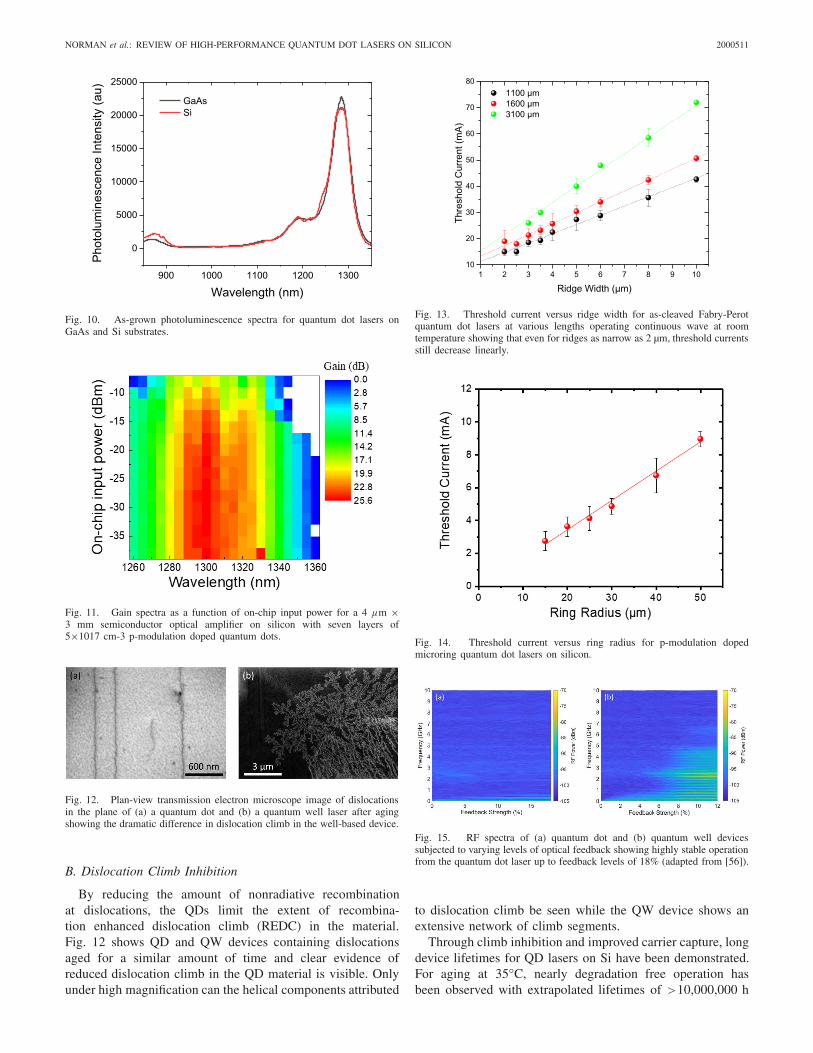
Fig. 14. Threshold current versus ring radius for p-modulation dopedmicroring quantum dot lasers on silicon.
Fig. 15. RF spectra of (a) quantum dot and (b) quantum well devicessubjected to varying levels of optical feedback showing highly stable operationfrom the quantum dot laser up to feedback levels of 18% (adapted from [56]).
to dislocation climb be seen while the QW device shows anextensive network of climb segments.
Through climb inhibition and improved carrier capture, longdevice lifetimes for QD lasers on Si have been demonstrated.For aging at 35◦C, nearly degradation free operation hasbeen observed with extrapolated lifetimes of >10,000,000 h

2000511 IEEE JOURNAL OF QUANTUM ELECTRONICS, VOL. 55, NO. 2, APRIL 2019
Fig. 16. (a) Optical spectrum from a quantum dot mode-locked laser grown on silicon with (inset) RF electrical spectrum. (b) Single sideband phase noiseplot showing record low timing jitter. (c) Relative intensity noise (RIN) spectrum for the entire mode-locked laser spectrum and for an individual comb lineafter amplification. Adapted from [58].
reported [53]. At 60◦C, further improvements are still neededto achieve commercial viability, but recent results utilizingpMD active regions have shown promising extrapolated life-times of ∼100,000 h in some devices.
C. Device Miniaturization
For integrated applications, device miniaturization is desir-able to increase integration density, but as devices shrink theeffects of surfaces, which act as extended planar defects, beginto limit performance. In QD devices, the same properties thatreduce sensitivity to dislocations, also reduce their sensitivityto recombination at device sidewalls and other surfaces. In QWlasers the minimum device size is limited by their effectivein-plane diffusion length of several microns which causesincreasing threshold currents as the laser cavity shrinks inwidth, but in QD layers, the in-plane diffusion length is∼1 μm. Due to limited in-plane diffusion, QD lasers showlinearly decreasing thresholds for ridge widths down to 2 μmas depicted in Fig. 13.
Further emphasis of the scalability of QD devices can beseen in the high performance of micron-scale ring resonatorcavities. In devices with uid active regions, ultralow thresholdsunder 1 mA have been demonstrated on Si substrates by scal-ing to rings with radii of 4 μm [55]. Devices with pMD in theactive region analogous to the Fabry-Perot results in Fig. 13 areshown in Fig. 14. The smallest devices, with a radiusof 15 μm m, show threshold currents approaching 2 mA.
VI. HIGH LASER STABILITY
A. Stability Against Optical Feedback
As mentioned above, the ultralow values of the linewidthenhancement factor lead to highly stable operation underoptical feedback. In a direct comparison of QD lasers onSi with 2×108 cm−2 dislocation density and >35 meVPL FWHM showed similar relative intensity noise (RIN) at10 dB higher feedback levels relative to heterogeneous QWdevices [7]. After improving the material quality of the QDlasers to 7×106 cm−2 dislocation density and PL FWHM to∼30 meV, the stability against feedback became much morepronounced with stable operation being observed even with90% of the light reflected back to the cavity (estimated to be18% feedback after coupling losses) [56].
B. Stable Mode-Locking
The independence of each QD results in low noisemode-locked lasers. Since each inhomogeneously broadenedQD acts as an independent emitter, the multiple modes lasingsimultaneously with locked phase in a MLL will not competefor gain as they correspond to different subsets of the overalldot distribution. On silicon, heterogeneous devices have beendemonstrated with simultaneous error free transmission from15 channels [57], and epitaxial devices on silicon have shown4.1 Tb/s transmission using a single MLL grown on Si witha 3dB bandwidth including 58 comb lines (Fig. 16a) thatwere independently modulated [58]. The latter device showeda record low timing jitter of 286 fs from 100 kHz to 100 MHz(Fig. 16(b)) and low average RIN of −133 dB/Hz for individ-ual comb lines from 10 MHz to 10 GHz (Fig. 16(c). Theseperformance levels provide further evidence that epitaxial QDlasers on silicon can rival the performance of native substratedevices.
VII. CONCLUSION
In summary, quantum dot lasers enable substantial perfor-mance improvements over quantum well devices due to theirunique atom-like energy level structure properties that can befinely tuned by changing growth conditions. Their discretedensity of states and inhomogeneously broadened gain leadto lasers with low threshold, high continuous wave operatingtemperature, ultrahigh stability against optical feedback, andultrafast gain recovery. Each of these concepts has been exper-imentally demonstrated, and due to the reduced sensitivityof quantum dots to crystalline defects, their advantageousproperties are also starting to be shown for epitaxially inte-grated lasers on silicon, enabling significant improvements inmanufacturing scalability.
ACKNOWLEDGMENT
The authors acknowledge valuable discussions with KunalMukherjee, Jennifer Selvidge, and Frederic Grillot.
REFERENCES
[1] Y. Arakawa and H. Sakaki, “Multidimensional quantum well laser andtemperature dependence of its threshold current,” Appl. Phys. Lett.,vol. 40, no. 11, pp. 939–941, 1982.
[2] N. Kirstaedter et al., “Low threshold, large To injection laser emis-sion from (InGa)As quantum dots,” Electron. Lett., vol. 30, no. 17,pp. 1416–1417, Aug. 1994.

NORMAN et al.: REVIEW OF HIGH-PERFORMANCE QUANTUM DOT LASERS ON SILICON 2000511
[3] R. Mirin, A. Gossard, and J. Bowers, “Room temperature lasing fromInGaAs quantum dots,” Electron. Lett., vol. 32, no. 18, p. 1732,Aug. 1996.
[4] D. Bimberg and U. W. Pohl, “Quantum dots: Promises and accomplish-ments,” Mater. Today, vol. 14, no. 9, pp. 388–397, 2011.
[5] T. Kageyama et al., “Extremely high temperature (220 °C) continuous-wave operation of 1300-nm-range quantum-dot lasers,” in Proc. Conf.Lasers Electro-Opt. Eur. 12th Eur. Quantum Electron. Conf. (CLEOEUROPE/EQEC), May 2011, p. 1.
[6] A. Y. Liu, S. Srinivasan, J. Norman, A. C. Gossard, and J. E. Bowers,“Quantum dot lasers for silicon photonics,” Photon. Res., vol. 3, no. 5,pp. B1–B9, 2015.
[7] A. Y. Liu, T. Komljenovic, M. L. Davenport, A. C. Gossard, andJ. E. Bowers, “Reflection sensitivity of 1.3 μm quantum dotlasers epitaxially grown on silicon,” Opt. Express, vol. 25, no. 9,pp. 9535–9543, 2017.
[8] H. Schmeckebier and D. Bimberg, “Quantum-dot semiconductor opticalamplifiers for energy-efficient optical communication,” in Proc. GreenPhoton. Electron., Nov. 2017, pp. 37–74.
[9] D. Arsenijevic and D. Bimberg, “Quantum-dot mode-locked lasers:Sources for tunable optical and electrical pulse combs,” in Proc. GreenPhoton. Electron., Nov. 2017, pp. 75–106.
[10] J. C. Norman, D. Jung, Y. Wan, and J. E. Bowers, “Perspective:The future of quantum dot photonic integrated circuits,” APL Photon.,vol. 3, no. 3, Mar. 2018, Art. no. 030901.
[11] A. Y. Liu and J. Bowers, “Photonic integration with epitaxial III–Von silicon,” IEEE J. Sel. Topics Quantum Electron., vol. 24, no. 6,Nov./Dec. 2018.
[12] R. P. Mirin, J. P. Ibbetson, K. Nishi, A. C. Gossard, and J. E. Bowers,“1.3 μm photoluminescence from InGaAs quantum dots on GaAs,”Appl. Phys. Lett., vol. 67, no. 25, pp. 3795–3797, 1995.
[13] A. J. Zilkie et al., “Carrier dynamics of quantum-dot, quantum-dash, andquantum-well semiconductor optical amplifiers operating at 1.55 μm,”IEEE J. Quantum Electron., vol. 43, no. 11, pp. 982–991, Nov. 2007.
[14] V. Shchukin, N. N. Ledentsov, and D. Bimberg, Epitaxy of Nanostruc-tures. New York, NY, USA: Springer, 2013.
[15] O. Stier, M. Grundmann, and D. Bimberg, “Electronic and opticalproperties of strained quantum dots modeled by 8-band k·p theory,”Phys. Rev. B, vol. 59, nos. 8–15, p. 5688, 1999.
[16] P. Jayavel et al., “Control of optical polarization anisotropy in edgeemitting luminescence of InAs/GaAs self-assembled quantum dots,”Appl. Phys. Lett., vol. 84, no. 11, pp. 1820–1822, 2004.
[17] K. Nishi, K. Takemasa, M. Sugawara, and Y. Arakawa, “Developmentof quantum dot lasers for data-com and silicon photonics applications,”IEEE J. Sel. Topics Quantum Electron., vol. 23, no. 6, Nov./Dec. 2017,Art. no. 1901007.
[18] A. O. Kosogov et al., “Structural and optical properties of InAs–GaAsquantum dots subjected to high temperature annealing ,” Appl. Phys.Lett., vol. 69, no. 20, pp. 3072–3074, 1996.
[19] Q. Li, K. W. Ng, and K. M. Lau, “Growing antiphase-domain-free GaAsthin films out of highly ordered planar nanowire arrays on exact (001)silicon,” Appl. Phys. Lett., vol. 106, no. 7, Feb. 2015, Art. no. 072105.
[20] J. Kwoen, B. Jang, J. Lee, T. Kageyama, K. Watanabe, and Y. Arakawa,“All MBE grown InAs/GaAs quantum dot lasers on on-axis Si (001),”Opt. Express, vol. 26, no. 9, pp. 11568–11576, 2018.
[21] R. Alcotte et al., “Epitaxial growth of antiphase boundary free GaAslayer on 300 mm Si(001) substrate by metalorganic chemical vapourdeposition with high mobility,” Apl Mater., vol. 4, no. 4, Apr. 2016,Art. no. 046101.
[22] W.-Q. Wei et al., “InAs QDs on (111)-faceted Si (001) hollow substrateswith strong emission at 1300?nm and 1550 nm,” Appl. Phys. Lett.,vol. 113, no. 5, 2018, Art. no. 053107.
[23] Y. Urino et al., “First demonstration of Athermal silicon optical inter-posers with quantum dot lasers operating up to 125 °C,” J. Lightw.Technol., vol. 33, no. 6, pp. 1223–1229, Mar. 2015.
[24] Z. Lu, J. R. Liu, S. Raymond, P. J. Poole, P. J. Barrios, and D. Poitras,“312-fs pulse generation from a passive C-band InAs/InP quantum dotmode-locked laser,” Opt. Express, vol. 16, no. 14, pp. 10835–10840,2008.
[25] A. Zeghuzi et al., “25 Gbit/s differential phase-shift-keying signalgeneration using directly modulated quantum-dot semiconductor opticalamplifiers,” Appl. Phys. Lett., vol. 106, no. 21, 2015, Art. no. 213501.
[26] O. B. Shchekin and D. G. Deppe, “Low-threshold high-T01.3-μm InAsquantum-dot lasers due to p-type modulation doping of the activeregion,” IEEE Photon. Technol. Lett., vol. 14, no. 9, pp. 1231–1233,Sep. 2002.
[27] O. B. Shchekin, J. Ahn, and D. G. Deppe, “High temperature perfor-mance of self-organised quantum dot laser with stacked p-doped activeregion,” Electron. Lett., vol. 38, no. 14, pp. 712–713, Jul. 2002.
[28] P. M. Smowton, I. C. Sandall, H. Liu, and M. Hopkinson, “Gain inp-doped quantum dot lasers,” J. Appl. Phys., vol. 101, no. 1, 2007,Art. no. 013107.
[29] Z. Zhang, D. Jung, J. C. Norman, P. Patel, W. W. Chow, andJ. E. Bowers, “Effects of modulation p-doping in InAs quantumdot lasers on silicon ” Appl. Phys. Lett., vol. 113, no. 6, 2018,Art. no. 061105.
[30] W. W. Chow and F. Jahnke, “On the physics of semiconductor quantumdots for applications in lasers and quantum optics,” Progr. QuantumElectron., vol. 37, no. 3, pp. 109–184, 2013.
[31] D. T. Cassidy, “Technique for measurement of the gain spectraof semiconductor diode lasers,” J. Appl. Phys., vol. 56, no. 11,pp. 3096–3099, 1984.
[32] S. Fathpour et al., “The role of Auger recombination in the temperature-dependent output characteristics (T∞) of p-doped 1.3 μm quantum dotlasers ,” Appl. Phys. Lett., vol. 85, no. 22, pp. 5164–5166, 2004.
[33] P. M. Smowton, A. George, I. C. Sandall, M. Hopkinson, andH.-Y. Liu, “Origin of temperature-dependent threshold current inp-doped and Undoped In(Ga)as quantum dot lasers,” IEEE J. Sel. TopicsQuantum Electron., vol. 14, no. 4, pp. 1162–1170, Jul./Aug. 2008.
[34] J. C. Norman et al., “High performance quantum dot lasers epitaxiallyintegrated on Si,” in Proc. 16th Quantum Commun. Quantum Imag.,vol. 10771, Art. no. 107710D.
[35] M. Sugawara, K. Mukai, and H. Shoji, “Effect of phonon bottleneckon quantum-dot laser performance,” Appl. Phys. Lett., vol. 71, no. 19,pp. 2791–2793, 1997.
[36] T. W. Berg, S. Bischoff, I. Magnusdottir, and J. Mork, “Ultrafastgain recovery and modulation limitations in self-assembled quantum-dot devices,” IEEE Photon. Technol. Lett., vol. 13, no. 6, pp. 541–543,Jun. 2001.
[37] K. Kim, J. Urayama, T. B. Norris, J. Singh, J. Phillips, andP. Bhattacharya, “Gain dynamics and ultrafast spectral hole burning inIn(Ga)As self-organized quantum dots,” Appl. Phys. Lett., vol. 81, no. 4,pp. 670–672, 2002.
[38] P. Bhattacharya et al., “Carrier dynamics and high-speed modulationproperties of tunnel injection InGaAs-GaAs quantum-dot lasers,” IEEEJ. Quantum Electron., vol. 39, no. 8, pp. 952–962, Aug. 2003.
[39] Z. Mi and P. Bhattacharya, “DC and dynamic characteristics of P-dopedand tunnel injection 1.65-μm InAs quantum-dash lasers grown on InP(001),” IEEE J. Quantum Electron., vol. 42, no. 12, pp. 1224–1232,Nov. 2006.
[40] Z. Mi, P. Bhattacharya, and S. Fathpour, “High-speed 1.3 μm tunnelinjection quantum-dot lasers,” Appl. Phys. Lett., vol. 86, no. 15, 2005,Art. no. 153109.
[41] J. Duan et al., “Semiconductor quantum dot lasers epitaxially grownon silicon with low linewidth enhancement factor,” Appl. Phys. Lett.,vol. 112, no. 25, 2018, Art. no. 251111.
[42] H. Huang et al., “Analysis of the optical feedback dynamics inInAs/GaAs quantum dot lasers directly grown on silicon,” J. Opt. Soc.Amer. B, vol. 35, no. 11, pp. 2780–2787, 2018.
[43] P. M. Smowton, E. J. Pearce, H. Schneider, W. W. Chow, andM. Hopkinson, “Filamentation and linewidth enhancement factor inInGaAs quantum dot lasers,” Appl. Phys. Lett., vol. 81, no. 17,pp. 3251–3253, 2002.
[44] Z. Zhang, D. Jung, J. C. Norman, P. Patel, W. W. Chow, andJ. E. Bowers, “Across zero continuously tunable linewidth enhancementfactor in 1.3 μm InAs quantum dot lasers on silicon,” in Proc. 26th Int.Semicond. Laser Conf., Santa Fe, NM, USA, 2018.
[45] T. Komljenovic, D. Huang, P. Pintus, M. A. Tran, M. L. Davenport,and J. E. Bowers, “Photonic integrated circuits using heterogeneousintegration on silicon,” Proc. IEEE, vol. 106, no. 12, pp. 2246–2257,Dec. 2018.
[46] S. Chen et al., “Electrically pumped continuous-wave 1.3 μmInAs/GaAs quantum dot lasers monolithically grown on on-axis Si (001)substrates,” Opt. Express, vol. 25, no. 5, pp. 4632–4639, 2017.
[47] B. Kunert, I. Németh, S. Reinhard, K. Volz, and W. Stolz, “Si (001)surface preparation for the antiphase domain free heteroepitaxial growthof GaP on Si substrate,” Thin Solid Films, vol. 517, no. 1, pp. 140–143,2008.
[48] M. Paladugu et al., “Site selective integration of III–V materials on Sifor nanoscale logic and photonic devices,” Crystal Growth Des., vol. 12,no. 10, pp. 4696–4702, 2012.

2000511 IEEE JOURNAL OF QUANTUM ELECTRONICS, VOL. 55, NO. 2, APRIL 2019
[49] H. Huang et al., “Crack-free GaAs epitaxy on Si by using midpatternedgrowth: Application to Si-based wavelength-selective photodetector,”J. Appl. Phys., vol. 104, no. 11, 2008, Art. no. 113114.
[50] M. Tang et al., “Optimizations of defect filter layers for 1.3-μmInAs/GaAs Quantum-Dot Lasers Monolithically grown on Si substrates,”IEEE J. Sel. Topics Quantum Electron., vol. 22, no. 6, Nov./Dec. 2016.
[51] D. Jung, P. G. Callahan, B. Shin, K. Mukherjee, A. C. Gossard, andJ. E. Bowers, “Low threading dislocation density GaAs growth on on-axis GaP/Si (001),” J. Appl. Phys., vol. 122, no. 22, p. 225703, 2017.
[52] E. Fitzgerald and N. Chand, “Epitaxial necking in GaAs grown on pre-pattemed Si substrates,” J. Electron. Mater., vol. 20, no. 7, pp. 839–853,1991.
[53] D. Jung et al., “Impact of threading dislocation density on the lifetimeof InAs quantum dot lasers on Si,” Appl. Phys. Lett., vol. 112, no. 15,2018, Art. no. 153507.
[54] M. Kuntz, G. Fiol, M. Laemmlin, C. Meuer, and D. Bimberg, “High-speed mode-locked quantum-dot lasers and optical amplifiers,” Proc.IEEE, vol. 95, no. 9, pp. 1767–1778, Sep. 2007.
[55] Y. Wan et al., “1.3 μm submilliamp threshold quantum dot micro-laserson Si,” Optica, vol. 4, no. 8, pp. 940–944, 2017.
[56] J. Duan et al., “1.3-μm reflection insensitive InAs/GaAs quantum dotlasers directly grown on silicon,” IEEE Photon. Technol. Lett., vol. 31,no. 5, pp. 345–348, Mar. 1, 2019.
[57] G. Kurczveil, C. Zhang, A. Descos, D. Liang, M. Fiorentino, andR. G. Beausoleil, “On-chip hybrid silicon quantum dot comb laserwith 14 error-free channels,” in Proc. IEEE Int. Semicond. Laser Conf.(ISLC), Santa Fe, NM, USA, Sep. 2018, pp. 1–2.
[58] S. Liu et al., “High-channel-count 20 GHz passively mode-lockedquantum dot laser directly grown on Si with 4.1 Tbit/s transmissioncapacity,” Optica, vol. 6, no. 2, pp. 128–134, 2018.
Justin C. Norman (S’14–M’18) received the B.S.degree in chemical engineering and physics from theUniversity of Arkansas at Fayetteville, Fayetteville,AR, USA, in 2013, and the Ph.D. degree in materialsfrom the University of California, Santa Barbara,with a focus on the epitaxial growth of quantum dotlasers for silicon photonics.
He is currently a Post-Doctoral Researcher withthe Institute for Energy Efficiency, University ofCalifornia. He focuses on the heteroepitaxy of III–Vmaterials on Si for photonic integration. His research
interests are in the growth of InAs quantum dots via molecular beam epitaxyfor applications in photonics and quantum electrodynamics. He was a recipientof the National Science Foundation Graduate Research Fellowship and theFrenkel Foundation Fellowship.
Daehwan Jung (M’16) received the Ph.D. degree inelectrical engineering from Yale University in 2016.He was a Post-Doctoral Researcher with the Uni-versity of California, Santa Barbara. He is currentlywith the Center for Opto-Electronic Materials andDevices, Korea Institute of Science and Technology,Seoul, South Korea. His current research project isto develop highly reliable, high-performance quan-tum dot lasers epitaxially grown on silicon forcommunication applications. His primary researchinterest is to study novel III–V materials growth for
high-performance optoelectronic and photonic devices.
Zeyu Zhang (S’17) received the B.S. degree inelectrical engineering from Clemson University, SC,USA, in 2015. He is currently pursuing the Ph.D.degree with the University of California, SantaBarbara, CA, USA.
His research interests include the characterizationand modeling of quantum dot laser epitaxially grownon silicon as well as passive–active integration ofphotonic devices with quantum dot active region onmonolithic III–V on silicon platform.
Yating Wan received the Ph.D. degree fromthe Department of Electrical and Computer Engi-neering, The Hong Kong University of Scienceand Technology, in2017. In2017, she joined Prof.J. E. Bowers’s Group, University of California, SantaBarbara, as a Post-Doctoral Research Associate. Herresearch interests include microcavity quantum dotoptoelectronics and silicon photonics. She was arecipient of the Ph.D. Research Excellence Awardduring 2016–2017.
Songtao Liu received the B.E. degree (Hons.) inelectronic information science and technology fromHenan University, Kaifeng, China, in 2012, and thePh.D. degree in microelectronics and solid stateelectronics from the University of Chinese Academyof Sciences, Beijing, China, 2017.
His Ph.D. dissertation was on the monolithicallyintegrated InP-based mode-locked lasers. He is cur-rently a Post-Doctoral Researcher with the Univer-sity of California, Santa Barbara, CA, USA. Hisresearch interests are in the field of photonic inte-
grated circuits, with an emphasis on monolithically integrated mode-lockedlasers and tunable lasers both on InP and silicon platforms.
Chen Shang received the B.S. degree in materialscience and engineering from Purdue University, IN,USA, in 2016. He is currently pursuing the Ph.D.degree in materials with the University of California,Santa Barbara, CA, USA.
His research interests are InAs quantum dots onInP lattice constant for telecom application and lowdefect density III–V buffer structure grown on Si viamolecular beam epitaxy. He was a recipient of thePeter J. Frenkel Foundation Fellowship.

NORMAN et al.: REVIEW OF HIGH-PERFORMANCE QUANTUM DOT LASERS ON SILICON 2000511
Robert W. Herrick (S’81–M’87–SM’05) receivedthe M.S.E.E. degree from the University of Illinoisin 1987. His career started at McDonnell Douglas,focusing on the early optoelectronic integrated cir-cuit and high-power laser research and development,where he involved in device modeling, mask design,and process development. After gaining an interestin reliability physics from the late Dr. R. G. Waters,he went to UCSB and did the first studies ofVCSEL degradation for his Ph.D. dissertation withProf. L. Coldren and Prof. P. Petroff. In the past
20 years, he has specialized in semiconductor laser reliability and failureanalysis. Since 2013, he has been with Intel, where he is currently responsiblefor laser reliability in the Silicon Photonic Product Division. He has been aLaser Reliability Engineer for many of the large fiber-optics companies inSilicon Valley, including HP/Agilent, Emcore, Finisar, and JDSU/Lumentum.He has authored or co-authored many of the most cited papers and invitedbook review chapters on the subject.
Weng W. Chow (F’09) received the Ph.D. degreein physics from The University of Arizona, with afocus on the research involving fluctuation phenom-ena in quantum optics.
He is currently a Member of the Technical Staffwith Sandia National Laboratories, where his pri-mary research involves applying microscopic the-ory to semiconductor laser development. Some ofthis work is described in two texts, Semiconductor-Laser Physics and Semiconductor-Laser Fundamen-tals: Physics of the Gain Materials. He is also an
Honorary Professor of physics with Cardiff University and a fellow withthe Institute for Quantum Science and Engineering, Texas A&M University.He is a fellow of OSA. He was a recipient of the Department of Energy,Basic Energy Science/Material Science Award, the J. J. Thompson Premium,the LEOS Distinguished Lecturer Award, the Alexander von HumboldtSenior Scientist Award, and the IEEE Photonics Society Quantum ElectronicsAward.
Arthur C. Gossard (SM’88–F’01–LF’12) was bornin Ottawa, IL, USA, in 1935. He received the B.A.degree (summa cum laude) in physics from HarvardUniversity, Cambridge, MA, USA, in 1956, andthe Ph.D. degree in physics from the University ofCalifornia at Berkeley, Berkeley, CA, USA, in 1960.
He was a Member of Technical Staff with AT&TBell Telephone Laboratories from 1960 to 1987.Since 1987, he has been with the University ofCalifornia at Santa Barbara, Santa Barbara, CA,USA, where he became a Professor in 1988. He dis-
covered the first nuclear magnetic resonance in ferromagnets. He also grewthe first alternate monolayer superlattices and created the first high mobilitymodulation doped semiconductors. He co-discovered fractional quantizationof the quantum Hall effect and the quantum confined Stark effect. His currentresearch interests center on molecular beam epitaxial crystal growth and onthe creation and application of artificially structured quantum materials.
Dr. Gossard is a member of the American Physical Society, the MaterialsResearch Society, the National Academy of Sciences, and the NationalAcademy of Engineering.
John E. Bowers (F’) received the M.S. and Ph.D.degrees from Stanford University. He was withAT&T Bell Laboratories. He is currently the Directorof the Institute for Energy Efficiency, Universityof California, Santa Barbara. He is also a Profes-sor with the Department of Electrical and Com-puter Engineering, University of California, and theDepartment of Materials, University of California.His research interests are primarily concerned withsilicon photonics, optoelectronic devices, opticalswitching and transparent optical networks, and
quantum dot lasers. He is a member of the National Academy of Engineeringand the National Academy of Inventors. He is a fellow of OSA and theAmerican Physical Society. He was a recipient of the IEEE Photonics Award,the OSA/IEEE Tyndall Award, the IEEE LEOS William Streifer Award, andthe South Coast Business and Technology Entrepreneur of the Year Award.