Embed Size (px)
Citation preview
Available online at www.sciencedirect.com
www.elsevier.com/locate/mee
Microelectronic Engineering 85 (2008) 161–167
A replication process of metallic micro-mold by usingparylene embossing and electroplating
Sung-Won Youn a,*, Hiroshi Goto a, Masaharu Takahashi a, Shoji Oyama b,1,Yasuhiko Oshinomi b,1, Kinya Matsutani b,1, Ryutaro Maeda a
a Advanced Manufacturing Research Institute, National Institute of Advanced Industrial Science and Technology (AIST),
1-2-1 Namiki, Tsukuba, Ibaraki 305-8564, Japanb Design Engineering Group, Engineering Department, Hirose Sensing Technology (HST) Co. Ltd., Kaneko No. 2 Building 8F,
2-6-23, Shinyokohama, Kohoku-ku, Yokohama-shi, Kanagawa 222-0033, Japan
Received 19 February 2007; accepted 7 May 2007Available online 16 May 2007
Abstract
This study demonstrated a replication process for metallic micro-mold that combines the parylene-C (poly-chloro-p-xylylene C) hot-embossing and electroplating techniques. A nickel original master was fabricated using the deep RIE silicon etching followed by the elec-troplating process. Then, the patterned fields composed of arrays of 25 lm-high, 10 lm-wide and 1 mm-long lines with 10 lm spacing innickel molds were successfully replicated on the 60 lm-thick parylene-C films by the hot-emboss process. Under complete filling condi-tions, the deviation of the replicated micropattern was less than 2.4%. The electroplated copper successfully filled parylene-C replica mas-ter patterns with the aspect ratio of 2.5 without the void formation by both adding organic addictives and controlling the seed layerthickness. After electroplating, the copper micro-mold could be successfully separated from the parylene-C replica master.� 2007 Elsevier B.V. All rights reserved.
Keywords: Metallic micro-mold; Hot-embossing; Lithography; Parylene-C (poly-chloro-p-xylylene C)
1. Introduction
For decades, hot-embossing (or thermal nanoimprintlithography) techniques have been utilized extensively forthe definition of nano/micro-features with a high through-put at a low cost [1–8]. Recently, hot-embossing techniqueshave been applied not only to the formation of micropat-tern but also to the high volume production of micro-devices such as micro-reactors [2], micro-fluidic systems[9] and micro-optical devices (e.g., diffraction gratings,waveguides, micro-ring resonators and Mach–Zehnderinterferometers) [10,11]. Furthermore, several kinds oflarge area processing methods such as the step-and-stamp[3], rolling [12] and flat-large mold [4,13] embossing tech-
0167-9317/$ - see front matter � 2007 Elsevier B.V. All rights reserved.doi:10.1016/j.mee.2007.05.005
* Corresponding author. Tel.: +81 29 861 7849; fax: +81 29 861 7167.E-mail address: [email protected] (S.-W. Youn).
1 Tel.: +81 45 472 4727; fax: +81 45 472 4962.
niques are being actively studied for the further progressof hot-embossing technologies. Nevertheless, there stillremain other critical issues that need to be more studiedfor the acceptance of hot-embossing technologies in indus-trial applications. One of them is the relatively high cost formold fabrication. Here, we were especially interested inlow-cost processes for the fabrication of metallic molds.Generally, fabrications of metallic micro-molds are per-formed by the well-developed silicon micromachining pro-cess (which allows for the fabrication of high-precisionmicrostructures by means of anisotropic etching, reactiveion etching and deposition) and a subsequent metal electro-plating. The cost for silicon micromachining is relativelyhigh and occupies a great portion of entire cost for metallicmold fabrication. Further, a silicon master cannot bereused as it is removed by a KOH etching after electroplat-ing. Our experiences have shown that generally used micro-molds (e.g, silicon, silicon oxide and metal molds) did not
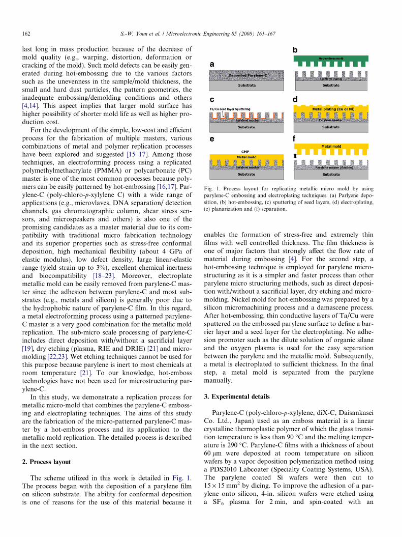
Fig. 1. Process layout for replicating metallic micro mold by usingparylene-C embossing and electroplating techniques. (a) Parlyene depo-sition, (b) hot-embossing, (c) sputtering of seed layers, (d) electroplating,(e) planarization and (f) separation.
162 S.-W. Youn et al. / Microelectronic Engineering 85 (2008) 161–167
last long in mass production because of the decrease ofmold quality (e.g., warping, distortion, deformation orcracking of the mold). Such mold defects can be easily gen-erated during hot-embossing due to the various factorssuch as the unevenness in the sample/mold thickness, thesmall and hard dust particles, the pattern geometries, theinadequate embossing/demolding conditions and others[4,14]. This aspect implies that larger mold surface hashigher possibility of shorter mold life as well as higher pro-duction cost.
For the development of the simple, low-cost and efficientprocess for the fabrication of multiple masters, variouscombinations of metal and polymer replication processeshave been explored and suggested [15–17]. Among thosetechniques, an electroforming process using a replicatedpolymethylmethacrylate (PMMA) or polycarbonate (PC)master is one of the most common processes because poly-mers can be easily patterned by hot-embossing [16,17]. Par-ylene-C (poly-chloro-p-xylylene C) with a wide range ofapplications (e.g., microvlaves, DNA separation/ detectionchannels, gas chromatographic column, shear stress sen-sors, and microspeakers and others) is also one of thepromising candidates as a master material due to its com-patibility with traditional micro fabrication technologyand its superior properties such as stress-free conformaldeposition, high mechanical flexibility (about 4 GPa ofelastic modulus), low defect density, large linear-elasticrange (yield strain up to 3%), excellent chemical inertnessand biocompatibility [18–23]. Moreover, electroplatemetallic mold can be easily removed from parylene-C mas-ter since the adhesion between parylene-C and most sub-strates (e.g., metals and silicon) is generally poor due tothe hydrophobic nature of parylene-C film. In this regard,a metal electroforming process using a patterned parylene-C master is a very good combination for the metallic moldreplication. The sub-micro scale processing of parylene-Cincludes direct deposition with/without a sacrificial layer[19], dry etching (plasma, RIE and DRIE) [21] and micro-molding [22,23]. Wet etching techniques cannot be used forthis purpose because parylene is inert to most chemicals atroom temperature [21]. To our knowledge, hot-embosstechnologies have not been used for microstructuring par-ylene-C.
In this study, we demonstrate a replication process formetallic micro-mold that combines the parylene-C emboss-ing and electroplating techniques. The aims of this studyare the fabrication of the micro-patterned parylene-C mas-ter by a hot-emboss process and its application to themetallic mold replication. The detailed process is describedin the next section.
2. Process layout
The scheme utilized in this work is detailed in Fig. 1.The process began with the deposition of a parylene filmon silicon substrate. The ability for conformal depositionis one of reasons for the use of this material because it
enables the formation of stress-free and extremely thinfilms with well controlled thickness. The film thickness isone of major factors that strongly affect the flow rate ofmaterial during embossing [4]. For the second step, ahot-embossing technique is employed for parylene micro-structuring as it is a simpler and faster process than otherparylene micro structuring methods, such as direct deposi-tion with/without a sacrificial layer, dry etching and micro-molding. Nickel mold for hot-embossing was prepared by asilicon micromachining process and a damascene process.After hot-embossing, thin conductive layers of Ta/Cu weresputtered on the embossed parylene surface to define a bar-rier layer and a seed layer for the electroplating. No adhe-sion promoter such as the dilute solution of organic silaneand the oxygen plasma is used for the easy separationbetween the parylene and the metallic mold. Subsequently,a metal is electroplated to sufficient thickness. In the finalstep, a metal mold is separated from the parylenemanually.
3. Experimental details
Parylene-C (poly-chloro-p-xylylene, diX-C, DaisankaseiCo. Ltd., Japan) used as an emboss material is a linearcrystalline thermoplastic polymer of which the glass transi-tion temperature is less than 90 �C and the melting temper-ature is 290 �C. Parylene-C films with a thickness of about60 lm were deposited at room temperature on siliconwafers by a vapor deposition polymerization method usinga PDS2010 Labcoater (Specialty Coating Systems, USA).The parylene coated Si wafers were then cut to15 · 15 mm2 by dicing. To improve the adhesion of a par-ylene onto silicon, 4-in. silicon wafers were etched usinga SF6 plasma for 2 min, and spin-coated with an
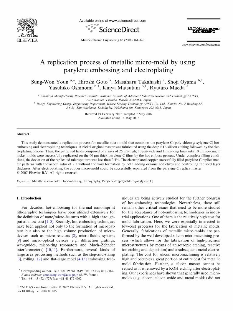
Fig. 2. Photograph and optical micrographs of nickel mold.
S.-W. Youn et al. / Microelectronic Engineering 85 (2008) 161–167 163
IPA:distilled H2O:KBM-503 100:100:1 solution before par-ylene deposition. Embossing tests were performed in a hot-emboss equipment, which is designed to emboss 3 · 3 cm2
samples. The maximum embossing temperature was700 �C, and the maximum press force was 2 kN. A pump-ing system allows embossing samples under vacuum, with apressure of 1 Pa inside the chamber. In the first step of hot-embossing process, the mold was pressed into a parylenefilm at a temperature well above the glass transition tem-perature (Tg) of the parylene, where the parylene has rela-tively low viscosity and can flow under applied pressure.The pressing pressure then held for a sufficient time toachieve complete filling. This hold time is a function ofboth material temperature and pressing force [8]. After nat-ural cooling to 80 �C (below Tg) the applied force wasreleased and the nickel mold was removed from the paryl-ene sample. Natural cooling was adapted since too fastcooling rate can cause cracking and delamination of paryl-ene film after cooling due to the large difference in the coef-ficient of thermal expansion between the silicon andparylene. Prior to hot-emboss tests, local flatness distor-tions in the mold and/or sample was evaluated using apressure-sensitive film (Prescale film, Fuji-Film Co.,Japan), and compensated by using spacers. A GC-1720(Sumitomo 3M, Japan) solution was used as a mold releaseagent. A chloronaphthalene solution (heated at >175 �C)and an oxygen plasma were used as mold cleaning agents.Thin metal layers of Ta/Cu were sputtered on theembossed parylene samples as conductive and conformalseed layers for electroplating copper. A profile meter (Tal-ysurf S4C, Taylor Hobson), an interferometric surface pro-filer (Zygo New View 5000) and a scanning electronmicroscopy (SEM) were used to obtain the morphologicaldata of the processed samples.
4. Results and discussion
The silicon master structure for mold was prepared by asilicon micromachining process such as deep reactive ionetching (DRIE). The channel width was fixed at 10 lmand the depth was fixed at 25 lm by the standard Boschetching cycles to achieve the aspect ratio of 2.5. The nickelmold with the size of 20 · 20 mm2 and the thickness of
Fig. 3. SEM images of arrays of 25 lm-high, 10 lm-wide and 1 mm-long limagnification image of (b).
0.3 mm was fabricated by the subsequent electroplatingprocess and by KOH etching of silicon master.
Figs. 2 and 3 show the photograph, optical micrographsand scanning electron microscopy (SEM) images of nickelmold that was fabricated using the deep RIE silicon etchingfollowed by the electroplating process. The nickel mold is20 · 20 mm2 in size and has arrays of 25 lm-high, 10 lm-wide and 1 mm-long lines with 10 lm spacing on its surfaceas known from the analysis results of optical interferome-try (Fig. 4). The mean height and surface roughness ofRa for the replicated micropatterns were 25.4 lm and131 nm, respectively. The thickness of the mold was0.3 mm that is thinner than generally used metallic molds.In general, a thinner mold provides better conformal con-tact with a sample surface and reduces the pressure neededfor the complete filling during the embossing step since it ismore flexible (or deformable) than thicker one [2].
For the hot-embossing tests, the pinhole-free parylene-Cfilm with thicknesses of about 60 lm was confirmly depos-ited on the silicon sample at room temperature. The thick-ness of a parylene film was set above twice of the masterstructure height (of mold) to achieve easy relaxation oflocalized strain for the fast material’s flow [24]. The filmthickness could be tuned by varying the quantity of a dim-mer and the deposition time.
nes with 10 lm spacing in nickel mold: (a) periphery; (b) middle; (c) a
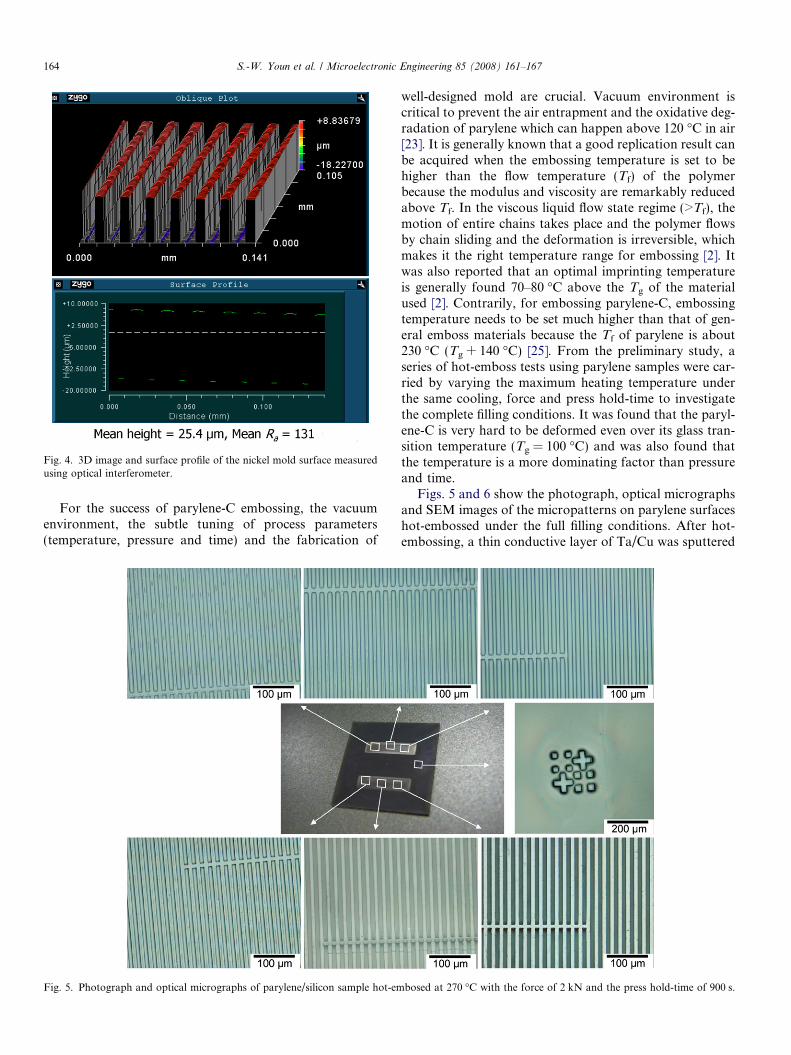
Fig. 4. 3D image and surface profile of the nickel mold surface measuredusing optical interferometer.
164 S.-W. Youn et al. / Microelectronic Engineering 85 (2008) 161–167
For the success of parylene-C embossing, the vacuumenvironment, the subtle tuning of process parameters(temperature, pressure and time) and the fabrication of
Fig. 5. Photograph and optical micrographs of parylene/silicon sample hot-em
well-designed mold are crucial. Vacuum environment iscritical to prevent the air entrapment and the oxidative deg-radation of parylene which can happen above 120 �C in air[23]. It is generally known that a good replication result canbe acquired when the embossing temperature is set to behigher than the flow temperature (Tf) of the polymerbecause the modulus and viscosity are remarkably reducedabove Tf. In the viscous liquid flow state regime (>Tf), themotion of entire chains takes place and the polymer flowsby chain sliding and the deformation is irreversible, whichmakes it the right temperature range for embossing [2]. Itwas also reported that an optimal imprinting temperatureis generally found 70–80 �C above the Tg of the materialused [2]. Contrarily, for embossing parylene-C, embossingtemperature needs to be set much higher than that of gen-eral emboss materials because the Tf of parylene is about230 �C (Tg + 140 �C) [25]. From the preliminary study, aseries of hot-emboss tests using parylene samples were car-ried by varying the maximum heating temperature underthe same cooling, force and press hold-time to investigatethe complete filling conditions. It was found that the paryl-ene-C is very hard to be deformed even over its glass tran-sition temperature (Tg = 100 �C) and was also found thatthe temperature is a more dominating factor than pressureand time.
Figs. 5 and 6 show the photograph, optical micrographsand SEM images of the micropatterns on parylene surfaceshot-embossed under the full filling conditions. After hot-embossing, a thin conductive layer of Ta/Cu was sputtered
bosed at 270 �C with the force of 2 kN and the press hold-time of 900 s.
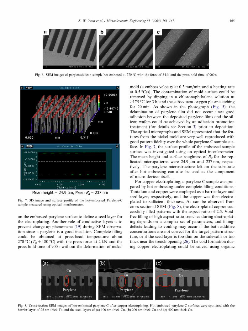
Fig. 6. SEM images of parylene/silicon sample hot-embosed at 270 �C with the force of 2 kN and the press hold-time of 900 s.
Fig. 7. 3D image and surface profile of the hot-embossed Parylene-Csample measured using optical interferometer.
S.-W. Youn et al. / Microelectronic Engineering 85 (2008) 161–167 165
on the embossed parylene surface to define a seed layer forthe electroplating. Another role of conductive layers is toprevent charge-up phenomena [19] during SEM observa-tion since a parylene is a good insulator. Complete fillingcould be obtained at press-head temperature about270 �C (Tg + 180 �C) with the press force at 2 kN and thepress hold-time of 900 s without the deformation of nickel
Fig. 8. Cross-section SEM images of hot-embossed parylene-C after copper ebarrier layer of 25 nm-thick Ta and the seed layers of (a) 100 nm-thick Cu, (b
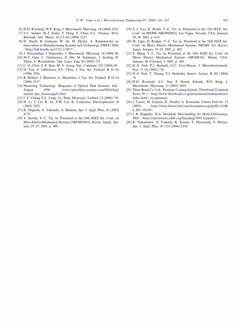
mold (a emboss velocity at 0.3 mm/min and a heating rateat 0.5 �C/s). The contamination of mold surface could beremoved by dipping in a chloronaphthalene solution at>175 �C for 3 h, and the subsequent oxygen plasma etchingfor 20 min. As shown in the photograph (Fig. 5), thedelamination of parylene film did not occur since goodadhesion between the deposited parylene films and the sil-icon wafers could be achieved by an adhesion promotiontreatment (for details see Section 3) prior to deposition.The optical micrographs and SEM represented that the fea-tures from the nickel mold are very well reproduced withgood pattern fidelity over the whole parylene-C sample sur-face. In Fig. 7, the surface profile of the embossed samplesurface was investigated using an optical interferometer.The mean height and surface roughness of Ra for the rep-licated micropatterns were 24.9 lm and 237 nm, respec-tively. The parylene microstructure left on the substrateafter hot-embossing can also be used as the componentof micro-devices itself.
For copper electroplating, a parylene-C sample was pre-pared by hot-embossing under complete filling conditions.Tantalum and copper were employed as a barrier layer andseed layer, respectively, and the copper was then electro-plated to sufficient thickness. As can be observed fromcross-sectional SEM (Fig. 8), the electroplated copper suc-cessfully filled patterns with the aspect ratio of 2.5. Void-free filling of high aspect ratio trenches during electroplat-ing depends on a complex set of parameters, and filling-defects leading to voiding may occur if the bath additiveconcentrations are not correct for the target pattern struc-ture, or if the seed layer is too thin on the sidewalls or toothick near the trench opening [26]. The void formation dur-ing copper electroplating could be solved using organic
lectroplating. Hot-embossed parylene-C surfaces were sputtered with the) 200 nm-thick Cu and (c) 400 nm-thick Cu.
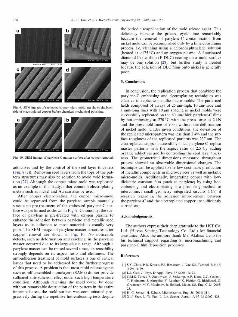
Fig. 10. SEM images of parylene-C master surface after copper removal.
Fig. 9. SEM images of replicated copper micro-mold; (a) shows the back-side of electroplated copper before chemical mechanical polishing.
166 S.-W. Youn et al. / Microelectronic Engineering 85 (2008) 161–167
addictives and by the control of the seed layer thickness(Fig. 8 (c)). Removing seed layers from the tops of the pat-tern structures may also be solution to avoid void forma-tion [27]. Although the copper micro-mold was replicatedas an example in this study, other common electroplatingmetals such as nickel and Au can also be used.
After copper electroplating, the copper micro-moldcould be separated from the parylene sample manuallysince a no pre-treatment of the embossed parylene-C sur-face was performed as shown in Fig. 9. Commonly, the sur-face of parylene is pre-treated with oxygen plasma toenhance the adhesion between parylene and metallic seedlayers as its adhesion to most materials is usually verypoor. The SEM images of parylene master structures aftercopper removal are shown in Fig. 10. No noticeabledefects, such as deformation and cracking, in the parylenemaster occurred due to its large-elastic range. Although aparylene master can be reused several times, its reusabilitystrongly depends on its aspect ratio and cleanness. Theanti-adhesion treatment of mold surfaces is one of criticalissues that need to be addressed for the further progressof this process. A problem is that most mold release agentssuch as self-assembled monolayers (SAMs) do not providesufficient anti-adhesion effect under such high temperaturecondition. Although releasing the mold could be donewithout remarkable destruction of the pattern in the entireimprinted area, the mold surface was contaminated pro-gressively during the repetitive hot-embossing tests despite
the periodic reapplication of the mold release agent. Thisdeficiency increase the process cycle time remarkablybecause the removal of parylene-C contamination fromnickel mold can be accomplished only by a time-consumingprocess, i.e, cleaning using a chloronaphthalene solution(heated at >175 �C) and an oxygen plasma. A fluorinateddiamond-like carbon (F-DLC) coating on a mold surfacemay be one solution [28], but further study is neededbecause the adhesion of DLC films onto nickel is generallypoor.
5. Conclusions
In conclusion, the replication process that combines theparylene-C embossing and electroplating techniques waseffective to replicate metallic micro-molds. The patternedfields composed of arrays of 25 lm-high, 10 lm-wide and1 mm-long lines with 10 lm spacing in nickel molds weresuccessfully replicated on the 60 lm-thick parylene-C filmsby hot-embossing at 270 �C with the press force at 2 kNand the press hold-time of 900 s without the deformationof nickel mold. Under given conditions, the deviation ofthe replicated micropattern was less than 2.4% and the sur-face roughness of the replicated patterns was 237 nm. Theelectroplated copper successfully filled parylene-C replicamaster patterns with the aspect ratio of 2.5 by addingorganic addictives and by controlling the seed layer thick-ness. The geometrical dimensions measured throughoutprocess showed no observable dimensional changes. Thetechnique can be applied to the low-cost mass productionof metallic components in micro-devices as well as metallicmicro-molds. Additionally, integrating copper with low-dielectric constant film (such as parylene) by using hot-embossing and electroplating is a promising method tointerconnect small geometry integrated circuits (ICs) ifresearch regarding the adhesion improvement betweenthe parylene-C and the electroplated copper are sufficientlycarried out.
Acknowledgements
The authors express their deep gratitude to the HST Co.Ltd. (Hirose Sensing Technology Co. Ltd.) for financialassistance. Also, the authors thank Mr. Akihisa Ueno forhis technical support regarding Si micromachining andparylene-C film deposition processes.
References
[1] S.Y. Chou, P.R. Krauss, P.J. Renstrom, J. Vac. Sci. Technol. B 14 (6)(1996) 4129.
[2] L.J. Guo, J. Phys. D Appl. Phys. 37 (2005) R123.[3] C.M.S. Torres, S. Zankovych, J. Seekamp, A.P. Kam, C.C. Cedeno,
T. Hoffmann, J. Ahopelto, F. Reuther, K. Pfeiffer, G. Bleidiessel, G.Gruetzner, M.V. Maximov, B. Heidari, Mater. Sci. Eng. C 23 (2003)23.
[4] H.-C. Scheer, H. Schulz, Microelectron. Eng. 56 (2001) 311.[5] X.-J. Shen, L.-W. Pan, L. Lin, Sensor. Actuat. A 97–98 (2002) 428.
S.-W. Youn et al. / Microelectronic Engineering 85 (2008) 161–167 167
[6] H.D. Rowland, W.P. King, J. Micromech. Microeng. 14 (2004) 1625.[7] V.C. Sunder, H.-J. Eisler, T. Deng, Y. Chan, E.L. Thomas, M.G.
Bawendi, Adv. Mater. 16 (23-24) (2004) 2137.[8] D. Hardt, B. Ganesan, W. Qi, M. Dirckx, A. Rzepniewski, in:
Innovation in Manufacturing Systems and Technology (IMST) 2004,<http://hdl.handle.net/1721.1/3917>.
[9] J. Narasimhan, I. Papautsky, J. Micromech. Microeng. 14 (2004) 96.[10] M.T. Gale, C. Gimkiewicz, S. Obi, M. Schnieper, J. Sochtig, H.
Thiele, S. Westenhofer, Opt. Laser. Eng. 43 (2005) 373.[11] C.-G. Choi, S.-P. Han, M.-Y. Jeong, Opt. Commun. 235 (2004) 69.[12] H. Tan, A. Gilbertson, S.Y. Chou, J. Vac. Sci. Technol. B 16 (6)
(1998) 3926.[13] B. Heidari, I. Maximov, L. Montelius, J. Vac. Sci. Technol. B 18 (6)
(2000) 3557.[14] Mastering Technology, Magazine of Optical Disk Systems, July–
August 1998. <www.opticaldisc-systems.com/98JulAug/optical_disc_featurespg51.htm>.
[15] C.Y. Chang, S.Y. Yang, J.L. Sheh, Microsyst. Technol. 12 (2006) 754.[16] H. Li, J. Lin, R. Su, Z.W. Cai, K. Uchiyama, Electrophoresis 26
(2005) 1825.[17] K. Deguchi, N. Takeuchi, A. Shimizu, Jpn. J. Appl. Phys. 41 (2002)
4178.[18] Y. Suzuki, Y.-C. Tai, in: Presented at the 16th IEEE Int. Conf. on
MicroElectroMechanical Systems (MEMS2003), Kyoto, Japan, Jan-uary 19–23, 2003, p. 486.
[19] T.-J. Yao, K. Walsh, Y.-C. Tai, in: Presented at the 15th IEEE. Int.Conf. on MEMS (MEMS2002), Las Vegas, Nevada, USA, January20–24, 2002, p. 614.
[20] M. Liger, D. Rodger, Y.-C. Tai, in: Presented at the 16th IEEE Int.Conf. on Micro Electro Mechanical Systems (MEMS ’03), Kyoto,Japan, January 19–23, 2003, p. 602.
[21] E. Meng, Y.-C. Tai, in: Presented at the 18th IEEE Int. Conf. onMicro Electro Mechanical Systems (MEMS‘05), Miami, USA,January 30–February 3, 2005, p. 568.
[22] H.-S. Noh, P.J. Hesketh, G.C. Frye-Mason, J. Microelectromech.Syst. 11 (6) (2002) 718.
[23] H.-S. Noh, Y. Huang, P.J. Hesketha, Sensor. Actuat. B 102 (2004)78.
[24] H.D. Rowland, A.C. Sun, P. Randy Schunk, W.P. King, J.Micromech. Microeng. 15 (2005) 2414.
[25] Three Bond Co. Ltd., Parylene Coating System, Threebond TechnicalNews. 39, 1. <http://www.threebond.co.jp/ja/technical/technicalnews/index.html> (in japanese).
[26] J. Tower, M. Gostein, K. Otsubo, A. Kawasaki, Future Fab Int. 15(2003). <http://www.future-fab.com/documents.asp?grID=216&d_ID=1912#>.
[27] C.R. Keppeler, D.A. Dornfeld, Micromilling for Mold Fabrication,2003, <http://repositories.cdlib.org/lma/pmg/2002 keppeler>.
[28] K. Nakamatsu, N. Yamada, K. Kanda, Y. Haruyama, S. Matsui,Jpn. J. Appl. Phys. 45 (35) (2006) L954.