Embed Size (px)
Citation preview
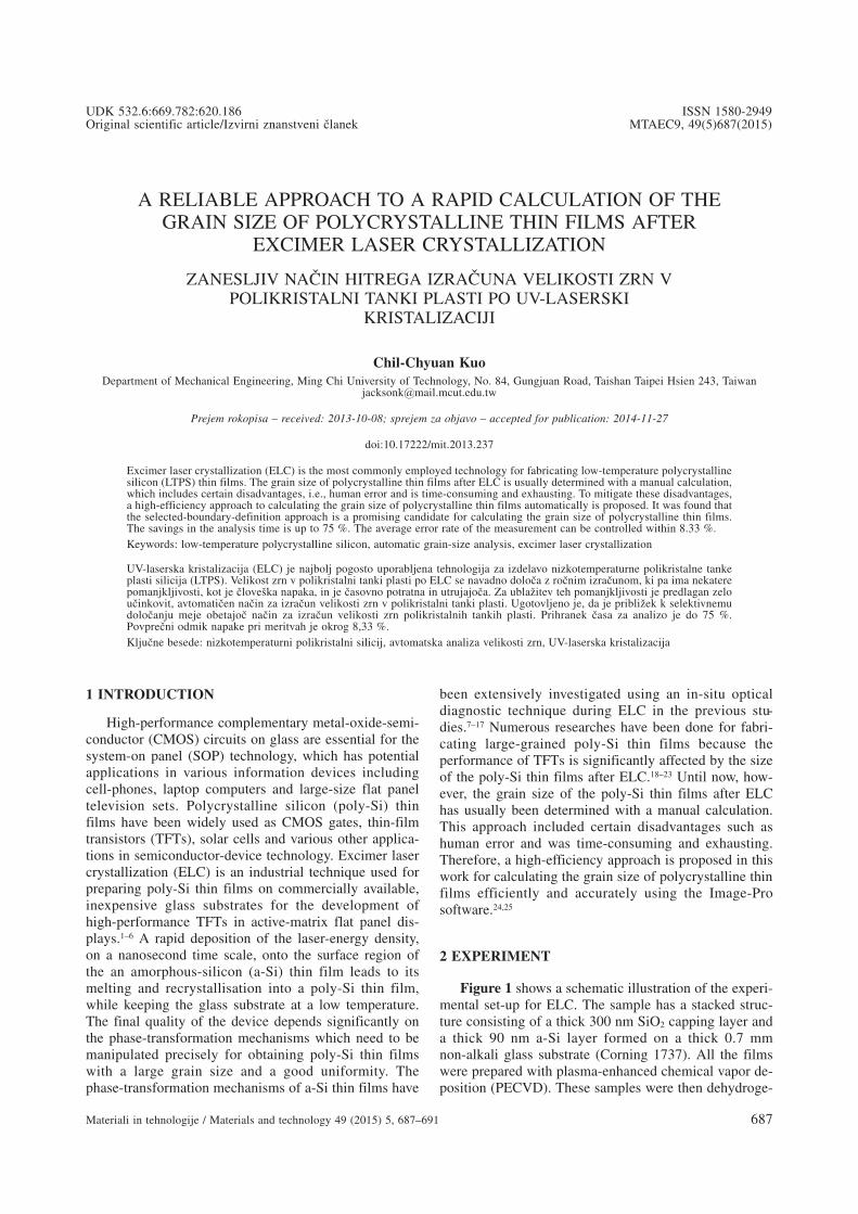
C. C. KUO: A RELIABLE APPROACH TO A RAPID CALCULATION OF THE GRAIN SIZE ...687–691
A RELIABLE APPROACH TO A RAPID CALCULATION OF THEGRAIN SIZE OF POLYCRYSTALLINE THIN FILMS AFTER
EXCIMER LASER CRYSTALLIZATION
ZANESLJIV NA^IN HITREGA IZRA^UNA VELIKOSTI ZRN VPOLIKRISTALNI TANKI PLASTI PO UV-LASERSKI
KRISTALIZACIJI
Chil-Chyuan KuoDepartment of Mechanical Engineering, Ming Chi University of Technology, No. 84, Gungjuan Road, Taishan Taipei Hsien 243, Taiwan
Prejem rokopisa – received: 2013-10-08; sprejem za objavo – accepted for publication: 2014-11-27
doi:10.17222/mit.2013.237
Excimer laser crystallization (ELC) is the most commonly employed technology for fabricating low-temperature polycrystallinesilicon (LTPS) thin films. The grain size of polycrystalline thin films after ELC is usually determined with a manual calculation,which includes certain disadvantages, i.e., human error and is time-consuming and exhausting. To mitigate these disadvantages,a high-efficiency approach to calculating the grain size of polycrystalline thin films automatically is proposed. It was found thatthe selected-boundary-definition approach is a promising candidate for calculating the grain size of polycrystalline thin films.The savings in the analysis time is up to 75 %. The average error rate of the measurement can be controlled within 8.33 %.Keywords: low-temperature polycrystalline silicon, automatic grain-size analysis, excimer laser crystallization
UV-laserska kristalizacija (ELC) je najbolj pogosto uporabljena tehnologija za izdelavo nizkotemperaturne polikristalne tankeplasti silicija (LTPS). Velikost zrn v polikristalni tanki plasti po ELC se navadno dolo~a z ro~nim izra~unom, ki pa ima nekaterepomanjkljivosti, kot je ~love{ka napaka, in je ~asovno potratna in utrujajo~a. Za ubla`itev teh pomanjkljivosti je predlagan zelou~inkovit, avtomati~en na~in za izra~un velikosti zrn v polikristalni tanki plasti. Ugotovljeno je, da je pribli`ek k selektivnemudolo~anju meje obetajo~ na~in za izra~un velikosti zrn polikristalnih tankih plasti. Prihranek ~asa za analizo je do 75 %.Povpre~ni odmik napake pri meritvah je okrog 8,33 %.Klju~ne besede: nizkotemperaturni polikristalni silicij, avtomatska analiza velikosti zrn, UV-laserska kristalizacija
1 INTRODUCTION
High-performance complementary metal-oxide-semi-conductor (CMOS) circuits on glass are essential for thesystem-on panel (SOP) technology, which has potentialapplications in various information devices includingcell-phones, laptop computers and large-size flat paneltelevision sets. Polycrystalline silicon (poly-Si) thinfilms have been widely used as CMOS gates, thin-filmtransistors (TFTs), solar cells and various other applica-tions in semiconductor-device technology. Excimer lasercrystallization (ELC) is an industrial technique used forpreparing poly-Si thin films on commercially available,inexpensive glass substrates for the development ofhigh-performance TFTs in active-matrix flat panel dis-plays.1–6 A rapid deposition of the laser-energy density,on a nanosecond time scale, onto the surface region ofthe an amorphous-silicon (a-Si) thin film leads to itsmelting and recrystallisation into a poly-Si thin film,while keeping the glass substrate at a low temperature.The final quality of the device depends significantly onthe phase-transformation mechanisms which need to bemanipulated precisely for obtaining poly-Si thin filmswith a large grain size and a good uniformity. Thephase-transformation mechanisms of a-Si thin films have
been extensively investigated using an in-situ opticaldiagnostic technique during ELC in the previous stu-dies.7–17 Numerous researches have been done for fabri-cating large-grained poly-Si thin films because theperformance of TFTs is significantly affected by the sizeof the poly-Si thin films after ELC.18–23 Until now, how-ever, the grain size of the poly-Si thin films after ELChas usually been determined with a manual calculation.This approach included certain disadvantages such ashuman error and was time-consuming and exhausting.Therefore, a high-efficiency approach is proposed in thiswork for calculating the grain size of polycrystalline thinfilms efficiently and accurately using the Image-Prosoftware.24,25
2 EXPERIMENT
Figure 1 shows a schematic illustration of the experi-mental set-up for ELC. The sample has a stacked struc-ture consisting of a thick 300 nm SiO2 capping layer anda thick 90 nm a-Si layer formed on a thick 0.7 mmnon-alkali glass substrate (Corning 1737). All the filmswere prepared with plasma-enhanced chemical vapor de-position (PECVD). These samples were then dehydroge-
Materiali in tehnologije / Materials and technology 49 (2015) 5, 687–691 687
UDK 532.6:669.782:620.186 ISSN 1580-2949Original scientific article/Izvirni znanstveni ~lanek MTAEC9, 49(5)687(2015)
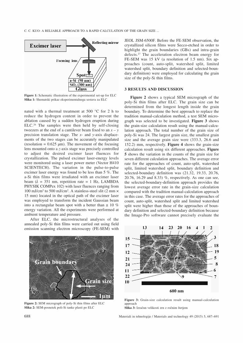
nated with a thermal treatment at 500 °C for 2 h toreduce the hydrogen content in order to prevent theablation caused by a sudden hydrogen eruption duringELC.26 The samples were then held by self-closingtweezers at the end of a cantilever beam fixed to an x – yprecision translation stage. The x- and y-axis displace-ments of the two stages can be accurately manipulated(resolution = 0.625 μm). The movement of the focusinglens mounted onto a z-axis stage was precisely controlledto adjust the desired excimer laser fluences forcrystallization. The pulsed excimer laser-energy levelswere monitored using a laser power meter (Vector H410SCIENTECH). The variation in the pulse-to-pulseexcimer laser energy was found to be less than 5 %. Thea-Si thin films were irradiated with an excimer laserbeam ( = 351 nm, repetition rate = 1 Hz, LAMBDAPHYSIK COMPex 102) with laser fluences ranging from100 mJ/cm2 to 500 mJ/cm2. A stainless-steel slit (2 mm ×15 mm) located in the optical path of the excimer laserwas employed to transform the incident Gaussian beaminto a rectangular beam spot with a better than ± 10 %energy variation. All the experiments were performed atambient temperature and pressure.
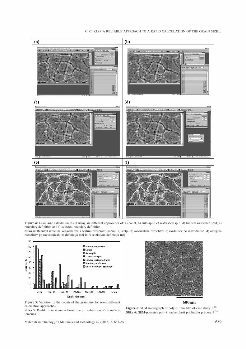
After ELC, the microstructural analyses of theannealed poly-Si thin films were carried out using fieldemission scanning electron microscopy (FE-SEM) with
JEOL JSM-6500F. Before the FE-SEM observation, thecrystallized silicon films were Secco-etched in order tohighlight the grain boundaries (GBs) and intra-graindefects.27 The acceleration electron beam energy forFE-SEM was 15 kV (a resolution of 1.5 nm). Six ap-proaches (count, auto-split, watershed split, limitedwatershed split, boundary definition and selected-boun-dary definition) were employed for calculating the grainsize of the poly-Si thin films.
3 RESULTS AND DISCUSSION
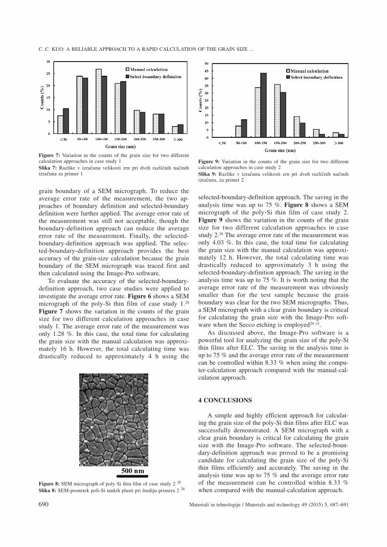
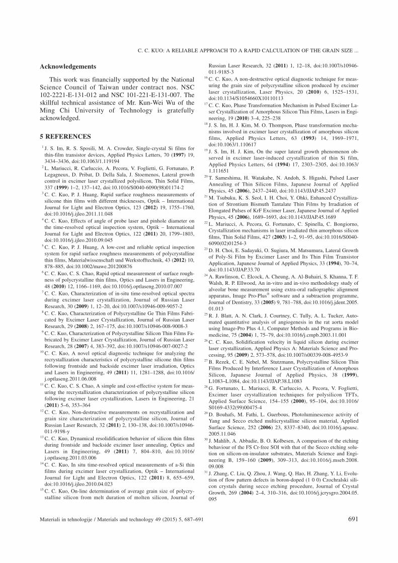
Figure 2 shows a typical SEM micrograph of thepoly-Si thin films after ELC. The grain size can bedetermined from the longest length inside the grainboundary. To determine the best approach to replace thetradition manual-calculation method, a test SEM micro-graph was selected to be investigated. Figure 3 showsthe grain-size calculation result using the manual-calcu-lation approach. The total number of the grain size ofpoly-Si was 24. The largest grain size, the smallest grainsize and the average grain size were (333.3, 26.6 and152.2) mm, respectively. Figure 4 shows the grain-sizecalculation result using six different approaches. Figure5 shows the variation in the counts of the grain size forseven different calculation approaches. The average errorrate for the approaches of count, auto-split, watershedsplit, limited watershed split, boundary definition andselected-boundary definition was (21.32, 19.33, 20.76,20.76, 16.29 and 8.33) %, respectively. As one can see,the selected-boundary-definition approach provides thelowest average error rate in the grain-size calculationcompared with the tradition manual-calculation approachin this case. The average error rates for the approaches ofcount, auto-split, watershed split and limited watershedsplit were higher than those of the approaches of boun-dary definition and selected-boundary definition becausethe Image-Pro software cannot precisely evaluate the
C. C. KUO: A RELIABLE APPROACH TO A RAPID CALCULATION OF THE GRAIN SIZE ...
688 Materiali in tehnologije / Materials and technology 49 (2015) 5, 687–691
Figure 3: Grain-size calculation result using manual-calculationapproachSlika 3: Izra~un velikosti zrn z ro~nim {tetjem
Figure 2: SEM micrograph of poly-Si thin films after ELCSlika 2: SEM-posnetek poli-Si tanke plasti po ELC
Figure 1: Schematic illustration of the experimental set-up for ELCSlika 1: Shematski prikaz eksperimentalnega sestava za ELC
C. C. KUO: A RELIABLE APPROACH TO A RAPID CALCULATION OF THE GRAIN SIZE ...
Materiali in tehnologije / Materials and technology 49 (2015) 5, 687–691 689
Figure 6: SEM micrograph of poly-Si thin film of case study 1 28
Slika 6: SEM-posnetek poli-Si tanke plasti pri {tudiju primera 1 28
Figure 5: Variation in the counts of the grain size for seven differentcalculation approachesSlika 5: Razlike v izra~unu velikosti zrn pri sedmih razli~nih na~inihizra~una
Figure 4: Grain-size calculation result using six different approaches of: a) count, b) auto-split, c) watershed split, d) limited watershed split, e)boundary definition and f) selected-boundary definitionSlika 4: Rezultat izra~una velikosti zrn s {estimi razli~nimi na~ini: a) {tetje, b) avtomatska razdelitev, c) razdelitev po razvodnicah, d) omejenarazdelitev po razvodnicah, e) definicija mej in f) selektivna definicija mej
grain boundary of a SEM micrograph. To reduce theaverage error rate of the measurement, the two ap-proaches of boundary definition and selected-boundarydefinition were further applied. The average error rate ofthe measurement was still not acceptable, though theboundary-definition approach can reduce the averageerror rate of the measurement. Finally, the selected-boundary-definition approach was applied. The selec-ted-boundary-definition approach provides the bestaccuracy of the grain-size calculation because the grainboundary of the SEM micrograph was traced first andthen calculated using the Image-Pro software.
To evaluate the accuracy of the selected-boundary-definition approach, two case studies were applied toinvestigate the average error rate. Figure 6 shows a SEMmicrograph of the poly-Si thin film of case study 1.28
Figure 7 shows the variation in the counts of the grainsize for two different calculation approaches in casestudy 1. The average error rate of the measurement wasonly 1.28 %. In this case, the total time for calculatingthe grain size with the manual calculation was approxi-mately 16 h. However, the total calculating time wasdrastically reduced to approximately 4 h using the
selected-boundary-definition approach. The saving in theanalysis time was up to 75 %. Figure 8 shows a SEMmicrograph of the poly-Si thin film of case study 2.Figure 9 shows the variation in the counts of the grainsize for two different calculation approaches in casestudy 2.28 The average error rate of the measurement wasonly 4.03 %. In this case, the total time for calculatingthe grain size with the manual calculation was approxi-mately 12 h. However, the total calculating time wasdrastically reduced to approximately 3 h using theselected-boundary-definition approach. The saving in theanalysis time was up to 75 %. It is worth noting that theaverage error rate of the measurement was obviouslysmaller than for the test sample because the grainboundary was clear for the two SEM micrographs. Thus,a SEM micrograph with a clear grain boundary is criticalfor calculating the grain size with the Image-Pro soft-ware when the Secco etching is employed29–31.
As discussed above, the Image-Pro software is apowerful tool for analyzing the grain size of the poly-Sithin films after ELC. The saving in the analysis time isup to 75 % and the average error rate of the measurementcan be controlled within 8.33 % when using the compu-ter-calculation approach compared with the manual-cal-culation approach.
4 CONCLUSIONS
A simple and highly efficient approach for calculat-ing the grain size of the poly-Si thin films after ELC wassuccessfully demonstrated. A SEM micrograph with aclear grain boundary is critical for calculating the grainsize with the Image-Pro software. The selected-boun-dary-definition approach was proved to be a promisingcandidate for calculating the grain size of the poly-Sithin films efficiently and accurately. The saving in theanalysis time was up to 75 % and the average error rateof the measurement can be controlled within 8.33 %when compared with the manual-calculation approach.
C. C. KUO: A RELIABLE APPROACH TO A RAPID CALCULATION OF THE GRAIN SIZE ...
690 Materiali in tehnologije / Materials and technology 49 (2015) 5, 687–691
Figure 9: Variation in the counts of the grain size for two differentcalculation approaches in case study 2Slika 9: Razlike v izra~unu velikosti zrn pri dveh razli~nih na~inihizra~una, za primer 2
Figure 7: Variation in the counts of the grain size for two differentcalculation approaches in case study 1Slika 7: Razlike v izra~unu velikosti zrn pri dveh razli~nih na~inihizra~una za primer 1
Figure 8: SEM micrograph of poly-Si thin film of case study 2 28
Slika 8: SEM-posnetek poli-Si tankih plasti pri {tudiju primera 2 28
Acknowledgements
This work was financially supported by the NationalScience Council of Taiwan under contract nos. NSC102-2221-E-131-012 and NSC 101-221-E-131-007. Theskillful technical assistance of Mr. Kun-Wei Wu of theMing Chi University of Technology is gratefullyacknowledged.
5 REFERENCES1 J. S. Im, R. S. Sposili, M. A. Crowder, Single-crystal Si films for
thin-film transistor devices, Applied Physics Letters, 70 (1997) 19,3434–3436, doi:10.1063/1.119194
2 L. Mariucci, R. Carluccio, A. Pecora, V. Foglietti, G. Fortunato, P.Legagneux, D. Pribat, D. Della Sala, J. Stoemenos, Lateral growthcontrol in excimer laser crystallized polysilicon, Thin Solid Films,337 (1999) 1–2, 137–142, doi:10.1016/S0040-6090(98)01174-2
3 C. C. Kuo, P. J. Huang, Rapid surface roughness measurements ofsilicone thin films with different thicknesses, Optik – InternationalJournal for Light and Electron Optics, 123 (2012) 19, 1755–1760,doi:10.1016/j.ijleo.2011.11.048
4 C. C. Kuo, Effects of angle of probe laser and pinhole diameter onthe time-resolved optical inspection system, Optik – InternationalJournal for Light and Electron Optics, 122 (2011) 20, 1799–1803,doi:10.1016/j.ijleo.2010.09.045
5 C. C. Kuo, P. J. Huang, A low-cost and reliable optical inspectionsystem for rapid surface roughness measurements of polycrystallinethin films, Materialwissenschaft und Werkstofftechnik, 43 (2012) 10,878–885, doi:10.1002/mawe.201200876
6 C. C. Kuo, C. S. Chao, Rapid optical measurement of surface rough-ness of polycrystalline thin films, Optics and Lasers in Engineering,48 (2010) 12, 1166–1169, doi:10.1016/j.optlaseng.2010.07.007
7 C. C. Kuo, Characterization of in-situ time-resolved optical spectraduring excimer laser crystallization, Journal of Russian LaserResearch, 30 (2009) 1, 12–20, doi:10.1007/s10946-009-9057-2
8 C. C. Kuo, Characterization of Polycrystalline Ge Thin Films Fabri-cated by Excimer Laser Crystallization, Journal of Russian LaserResearch, 29 (2008) 2, 167–175, doi:10.1007/s10946-008-9008-3
9 C. C. Kuo, Characterization of Polycrystalline Silicon Thin Films Fa-bricated by Excimer Laser Crystallization, Journal of Russian LaserResearch, 28 (2007) 4, 383–392, doi:10.1007/s10946-007-0027-2
10 C. C. Kuo, A novel optical diagnostic technique for analyzing therecrystallization characteristics of polycrystalline silicone thin filmsfollowing frontside and backside excimer laser irradiation, Opticsand Lasers in Engineering, 49 (2011) 11, 1281–1288, doi:10.1016/j.optlaseng.2011.06.008
11 C. C. Kuo, C. S. Chao, A simple and cost-effective system for meas-uring the recrystallization characterization of polycrystalline siliconfollowing excimer laser crystallization, Lasers in Engineering, 21(2011) 5–6, 353–364
12 C. C. Kuo, Non-destructive measurements on recrystallization andgrain size characterization of polycrystalline silicon, Journal ofRussian Laser Research, 32 (2011) 2, 130–138, doi:10.1007/s10946-011-9198-y
13 C. C. Kuo, Dynamical resolidification behavior of silicon thin filmsduring frontside and backside excimer laser annealing, Optics andLasers in Engineering, 49 (2011) 7, 804–810, doi:10.1016/j.optlaseng.2011.03.006
14 C. C. Kuo, In situ time-resolved optical measurements of a-Si thinfilms during excimer laser crystallization, Optik – InternationalJournal for Light and Electron Optics, 122 (2011) 8, 655–659,doi:10.1016/j.ijleo.2010.04.023
15 C. C. Kuo, On-line determination of average grain size of polycry-stalline silicon from melt duration of molten silicon, Journal of
Russian Laser Research, 32 (2011) 1, 12–18, doi:10.1007/s10946-011-9185-3
16 C. C. Kuo, A non-destructive optical diagnostic technique for meas-uring the grain size of polycrystalline silicon produced by excimerlaser crystallization, Laser Physics, 20 (2010) 6, 1525–1531,doi:10.1134/S1054660X10110113
17 C. C. Kuo, Phase Transformation Mechanism in Pulsed Excimer La-ser Crystallization of Amorphous Silicon Thin Films, Lasers in Engi-neering, 19 (2010) 3–4, 225–238
18 J. S. Im, H. J. Kim, M. O. Thompson, Phase transformation mecha-nisms involved in excimer laser crystallization of amorphous siliconfilms, Applied Physics Letters, 63 (1993) 14, 1969–1971,doi:10.1063/1.110617
19 J. S. Im, H. J. Kim, On the super lateral growth phenomenon ob-served in excimer laser-induced crystallization of thin Si film,Applied Physics Letters, 64 (1994) 17, 2303–2305, doi:10.1063/1.111651
20 T. Sameshima, H. Watakabe, N. Andoh, S. Higashi, Pulsed LaserAnnealing of Thin Silicon Films, Japanese Journal of AppliedPhysics, 45 (2006), 2437–2440, doi:10.1143/JJAP.45.2437
21 M. Tsubuku, K. S. Seol, I. H. Choi, Y. Ohki, Enhanced Crystalliza-tion of Strontium Bismuth Tantalate Thin Films by Irradiation ofElongated Pulses of KrF Excimer Laser, Japanese Journal of AppliedPhysics, 45 (2006), 1689–1693, doi:10.1143/JJAP.45.1689
22 L. Mariucci, A. Pecora, G. Fortunato, C. Spinella, C. Bongiorno,Crystallization mechanisms in laser irradiated thin amorphous siliconfilms, Thin Solid Films, 427 (2003) 1–2, 91–95, doi:10.1016/S0040-6090(02)01254-3
23 D. H. Choi, E. Sadayuki, O. Sugiura, M. Matsumura, Lateral Growthof Poly-Si Film by Excimer Laser and Its Thin Film TransistorApplication, Japanese Journal of Applied Physics, 33 (1994), 70–74,doi:10.1143/JJAP.33.70
24 A. Rawlinson, C. Elcock, A. Cheung, A. Al-Buhairi, S. Khanna, T. F.Walsh, R. P. Ellwood, An in-vitro and in-vivo methodology study ofalveolar bone measurement using extra-oral radiographic alignmentapparatus, Image Pro-Plus® software and a subtraction programme,Journal of Dentistry, 33 (2005) 9, 781–788, doi:10.1016/j.jdent.2005.01.013
25 R. J. Blatt, A. N. Clark, J. Courtney, C. Tully, A. L. Tucker, Auto-mated quantitative analysis of angiogenesis in the rat aorta modelusing Image-Pro Plus 4.1, Computer Methods and Programs in Bio-medicine, 75 (2004) 1, 75–79, doi:10.1016/j.cmpb.2003.11.001
26 C. C. Kuo, Solidification velocity in liquid silicon during excimerlaser crystallization, Applied Physics A: Materials Science and Pro-cessing, 95 (2009) 2, 573–578, doi:10.1007/s00339-008-4953-9
27 B. Rezek, C. E. Nebel, M. Stutzmann, Polycrystalline Silicon ThinFilms Produced by Interference Laser Crystallization of AmorphousSilicon, Japanese Journal of Applied Physics, 38 (1999),L1083–L1084, doi:10.1143/JJAP.38.L1083
28 G. Fortunato, L. Mariucci, R. Carluccio, A. Pecora, V. Foglietti,Excimer laser crystallization techniques for polysilicon TFTs,Applied Surface Science, 154–155 (2000), 95–104, doi:10.1016/S0169-4332(99)00475-4
29 D. Bouhafs, M. Fathi, L. Guerbous, Photoluminescence activity ofYang and Secco etched multicrystalline silicon material, AppliedSurface Science, 252 (2006) 23, 8337–8340, doi:10.1016/j.apsusc.2005.11.046
30 J. Mahlib, A. Abbadie, B. O. Kolbesen, A comparison of the etchingbehaviour of the FS Cr-free SOI with that of the Secco etching solu-tion on silicon-on-insulator substrates, Materials Science and Engi-neering B, 159–160 (2009), 309–313, doi:10.1016/j.mseb.2008.09.008
31 J. Zhang, C. Liu, Q. Zhou, J. Wang, Q. Hao, H. Zhang, Y. Li, Evolu-tion of flow pattern defects in boron-doped (1 0 0) Czochralski sili-con crystals during secco etching procedure, Journal of CrystalGrowth, 269 (2004) 2–4, 310–316, doi:10.1016/j.jcrysgro.2004.05.095
C. C. KUO: A RELIABLE APPROACH TO A RAPID CALCULATION OF THE GRAIN SIZE ...
Materiali in tehnologije / Materials and technology 49 (2015) 5, 687–691 691