Embed Size (px)
Citation preview
A platform for open innovation
English
TIA collaboration center2
Various R&D fields were grouped into three platforms.
Platforms and the fields of research and development Creating innovation using diverse technology seeds
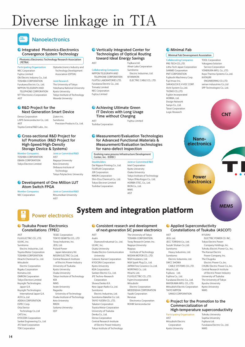
Nanoelectronics
Power electronics
MEMS
System and integration platform
Advanced material platform
Basic resource platform
1. Creation of global value2. Under one roof3. Independence/positive cycle4. Networking for “win-win”5. Education of next-generation scientists and engineers
Five principles
145 companies collaborated 12.2 billion yen spent for the projects62% of the spending was provided from public funding sources
602 external researchers participated 269 papers presented 167 patents published 888 graduate students collaborated
A cumulative total of 34 national projects were conducted at TIA 〔Figure of FY 2015〕
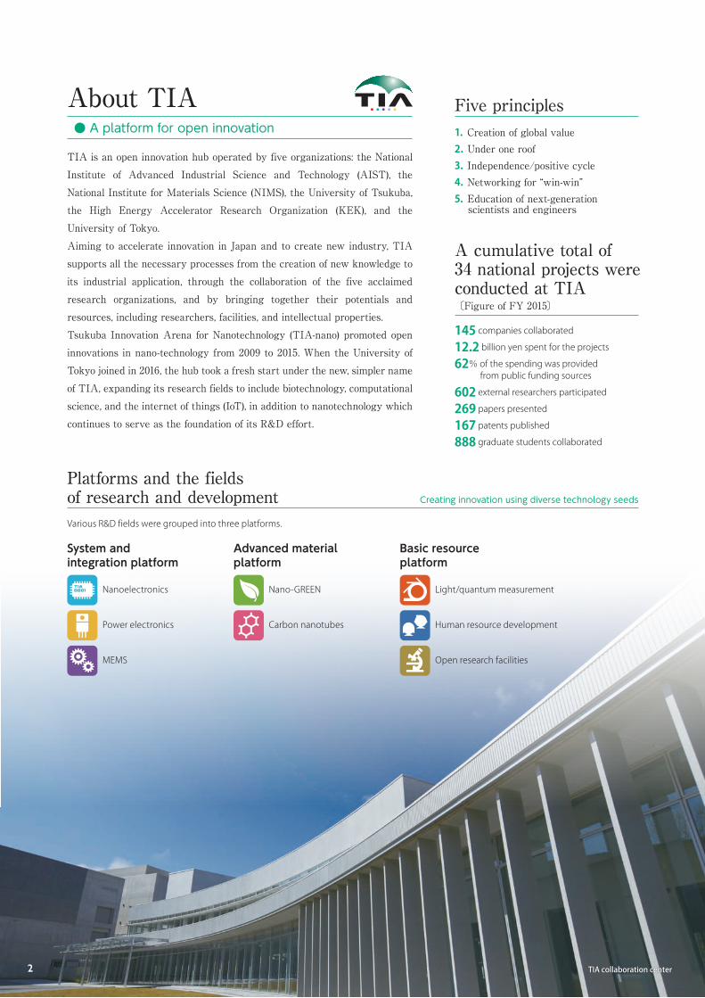
TIA is an open innovation hub operated by five organizations: the National Institute of Advanced Industrial Science and Technology (AIST), the National Institute for Materials Science (NIMS), the University of Tsukuba, the High Energy Accelerator Research Organization (KEK), and the University of Tokyo.Aiming to accelerate innovation in Japan and to create new industry, TIA supports all the necessary processes from the creation of new knowledge to its industrial application, through the collaboration of the five acclaimed research organizations, and by bringing together their potentials and resources, including researchers, facilities, and intellectual properties.Tsukuba Innovation Arena for Nanotechnology (TIA-nano) promoted open innovations in nano-technology from 2009 to 2015. When the University of Tokyo joined in 2016, the hub took a fresh start under the new, simpler name of TIA, expanding its research fields to include biotechnology, computational science, and the internet of things (IoT), in addition to nanotechnology which continues to serve as the foundation of its R&D effort.
About TIA● A platform for open innovation
Light/quantum measurement
Human resource development
Open research facilities
Nano-GREEN
Carbon nanotubes
3
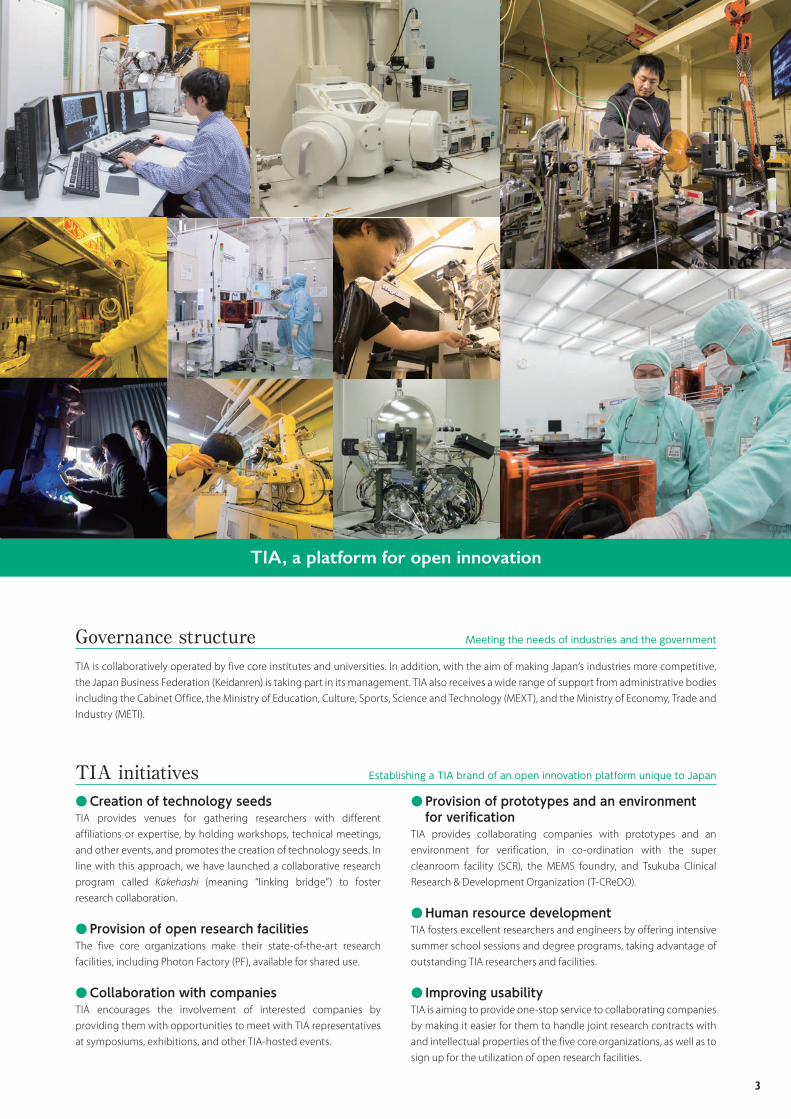
TIA, a platform for open innovation
●Creation of technology seedsTIA provides venues for gathering researchers with different affiliations or expertise, by holding workshops, technical meetings, and other events, and promotes the creation of technology seeds. In line with this approach, we have launched a collaborative research program called Kakehashi (meaning “linking bridge”) to foster research collaboration.
●Provision of open research facilitiesThe five core organizations make their state-of-the-art research facilities, including Photon Factory (PF), available for shared use.
●Collaboration with companiesTIA encourages the involvement of interested companies by providing them with opportunities to meet with TIA representatives at symposiums, exhibitions, and other TIA-hosted events.
●Provision of prototypes and an environment for verificationTIA provides collaborating companies with prototypes and an environment for verification, in co-ordination with the super cleanroom facility (SCR), the MEMS foundry, and Tsukuba Clinical Research & Development Organization (T-CReDO).
●Human resource developmentTIA fosters excellent researchers and engineers by offering intensive summer school sessions and degree programs, taking advantage of outstanding TIA researchers and facilities.
● Improving usabilityTIA is aiming to provide one-stop service to collaborating companies by making it easier for them to handle joint research contracts with and intellectual properties of the five core organizations, as well as to sign up for the utilization of open research facilities.
TIA initiatives Establishing a TIA brand of an open innovation platform unique to Japan
TIA is collaboratively operated by five core institutes and universities. In addition, with the aim of making Japan’s industries more competitive, the Japan Business Federation (Keidanren) is taking part in its management. TIA also receives a wide range of support from administrative bodies including the Cabinet Office, the Ministry of Education, Culture, Sports, Science and Technology (MEXT), and the Ministry of Economy, Trade and Industry (METI).
Governance structure Meeting the needs of industries and the government
4
TIA has been launching new projects since the University of Tokyo joined
TIA on April 1, 2016. These projects are not limited to the field of advanced
nanotechnology but include other research fields described in this and
the next pages. In addition, we have implemented a collaborative
research program called Kakehashi (meaning “linking bridge”).
New directions
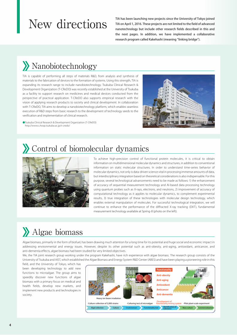
TIA is capable of performing all steps of materials R&D, from analysis and synthesis of materials to the fabrication of devices to the formation of systems. Using this strength, TIA is expanding its research range to include nanobiotechnology. Tsukuba Clinical Research & Development Organization (T-CReDO) was recently established at the University of Tsukuba as a facility to support research on medicines and medical devices conducted from the perspective of practical application. T-CReDO also supports empirical research with the vision of applying research products to society and clinical development. In collaboration with T-CReDO, TIA aims to develop a nanobiotechnology platform, which enables seamless execution of R&D steps from basic research to the development of technology seeds to the verification and implementation of clinical research. ●Tsukuba Clinical Research & Development Organization (T-CReDO) http://www.s.hosp.tsukuba.ac.jp/t-credo/
Nanobiotechnology
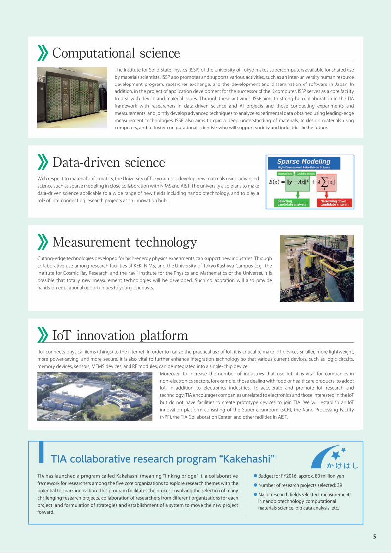
Algae biomass, primarily in the form of biofuel, has been drawing much attention for a long time for its potential and huge social and economic impact in addressing environmental and energy issues. However, despite its other potential such as anti-obesity, anti-aging, antioxidant, anticancer, and anti-dementia effects, algae biomass had been studied for very limited objectives.We, the TIA joint research group working under the program Kakehashi, have rich experience with algae biomass. The research group consists of the University of Tsukuba and AIST, which established the Algae Biomass and Energy System R&D Center (ABES) and have been playing a pioneering role in this field, and the University of Tokyo, which has been developing technology to add new functions to microalgae. The group aims to speedily discover new functions of algae biomass with a primary focus on medical and health fields, develop new markets, and implement new products and technologies in society.
Algae biomass
To achieve high-precision control of functional protein molecules, it is critical to obtain information on multidimensional molecular dynamics and structures, in addition to conventional information on static molecular structures. In order to understand time-series behavior of molecular dynamics, not only is data-driven science vital in processing immense amounts of data, but interdisciplinary integration based on theoretical considerations is also indispensable. For this purpose, several technological advancements need to be made as follows: 1) the enhancement of accuracy of sequential measurement technology and AI-based data processing technology using quantum probes such as X-rays, electrons, and neutrons, 2) improvement of accuracy of computational technology as it applies to molecular dynamics, to complement experimental results, 3) true integration of these technologies with molecular design technology, which enables external manipulation of molecules. For successful technological integration, we will continue to enhance the performance of the diffracted X-ray tracking (DXT), fundamental measurement technology available at Spring-8 (photo on the left).
Control of biomolecular dynamics
Heavy ion beam irradiation
-Culture collection of 3,000 strains
Algal collection Culture Crush/extract Functionality test Mass culture CommercializationIdentification of substance
Anti-obesity
Anti-aging
Antioxidant
Anticancer
Anti-dementia
-Culturing test of microalgae -Pilot plant-scale experiment-Development of functionality testing system
Functionality
5
TIA collaborative research program “Kakehashi”TIA has launched a program called Kakehashi (meaning “linking bridge” ), a collaborative framework for researchers among the five core organizations to explore research themes with the potential to spark innovation. This program facilitates the process involving the selection of many challenging research projects, collaboration of researchers from different organizations for each project, and formulation of strategies and establishment of a system to move the new project forward.
● Budget for FY2016: approx. 80 million yen
● Number of research projects selected: 39
● Major research fields selected: measurements in nanobiotechnology, computational materials science, big data analysis, etc.
Cutting-edge technologies developed for high-energy physics experiments can support new industries. Through collaborative use among research facilities of KEK, NIMS, and the University of Tokyo Kashiwa Campus (e.g., the Institute for Cosmic Ray Research, and the Kavli Institute for the Physics and Mathematics of the Universe), it is possible that totally new measurement technologies will be developed. Such collaboration will also provide hands-on educational opportunities to young scientists.
Measurement technology
The Institute for Solid State Physics (ISSP) of the University of Tokyo makes supercomputers available for shared use by materials scientists. ISSP also promotes and supports various activities, such as an inter-university human resource development program, researcher exchange, and the development and dissemination of software in Japan. In addition, in the project of application development for the successor of the K computer, ISSP serves as a core facility to deal with device and material issues. Through these activities, ISSP aims to strengthen collaboration in the TIA framework with researchers in data-driven science and AI projects and those conducting experiments and measurements, and jointly develop advanced techniques to analyze experimental data obtained using leading-edge measurement technologies. ISSP also aims to gain a deep understanding of materials, to design materials using computers, and to foster computational scientists who will support society and industries in the future.
Computational science
With respect to materials informatics, the University of Tokyo aims to develop new materials using advanced science such as sparse modeling in close collaboration with NIMS and AIST. The university also plans to make data-driven science applicable to a wide range of new fields including nanobiotechnology, and to play a role of interconnecting research projects as an innovation hub.
Data-driven science
IoT connects physical items (things) to the internet. In order to realize the practical use of IoT, it is critical to make IoT devices smaller, more lightweight, more power-saving, and more secure. It is also vital to further enhance integration technology so that various current devices, such as logic circuits, memory devices, sensors, MEMS devices, and RF modules, can be integrated into a single-chip device.
Moreover, to increase the number of industries that use IoT, it is vital for companies in non-electronics sectors, for example, those dealing with food or healthcare products, to adopt IoT, in addition to electronics industries. To accelerate and promote IoT research and technology, TIA encourages companies unrelated to electronics and those interested in the IoT but do not have facilities to create prototype devices to join TIA. We will establish an IoT innovation platform consisting of the Super cleanroom (SCR), the Nano-Processing Facility (NPF), the TIA Collaboration Center, and other facilities in AIST.
IoT innovation platform
Observed data
Selecting candidate answers
Narrowing down candidate answers
Candidate answers
6
System and integration platform
Nanoelectronics
We aim to apply IoT to society by creating smaller, power-saving, and high-performance IoT devices. To achieve this, we are developing three-dimensional packaging technology using through-silicon vias (TSVs) as a way to integrate semiconductor devices without relying on device miniaturization.
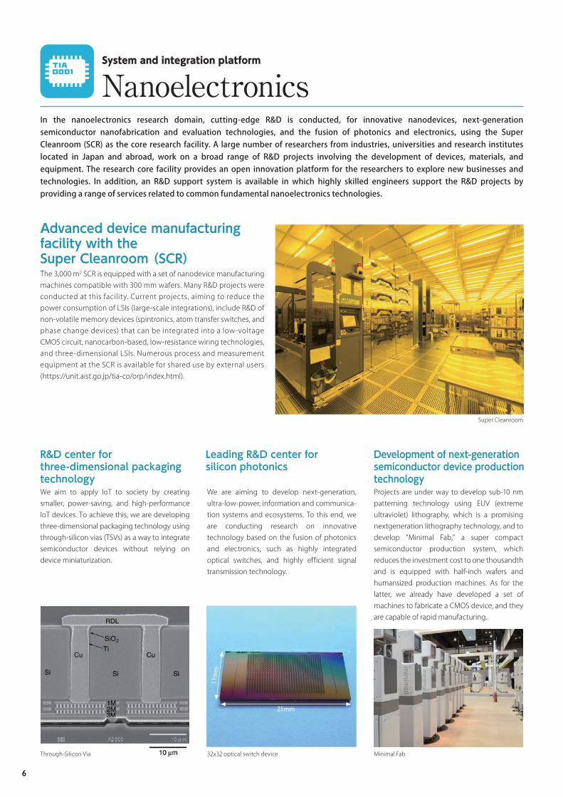
The 3,000 m2 SCR is equipped with a set of nanodevice manufacturing machines compatible with 300 mm wafers. Many R&D projects were conducted at this facility. Current projects, aiming to reduce the power consumption of LSIs (large-scale integrations), include R&D of non-volatile memory devices (spintronics, atom transfer switches, and phase change devices) that can be integrated into a low-voltage CMOS circuit, nanocarbon-based, low-resistance wiring technologies, and three-dimensional LSIs. Numerous process and measurement equipment at the SCR is available for shared use by external users (https://unit.aist.go.jp/tia-co/orp/index.html).
In the nanoelectronics research domain, cutting-edge R&D is conducted, for innovative nanodevices, next-generation semiconductor nanofabrication and evaluation technologies, and the fusion of photonics and electronics, using the Super Cleanroom (SCR) as the core research facility. A large number of researchers from industries, universities and research institutes located in Japan and abroad, work on a broad range of R&D projects involving the development of devices, materials, and equipment. The research core facility provides an open innovation platform for the researchers to explore new businesses and technologies. In addition, an R&D support system is available in which highly skilled engineers support the R&D projects by providing a range of services related to common fundamental nanoelectronics technologies.
R&D center for three-dimensional packaging technology
Advanced device manufacturing facility with the Super Cleanroom (SCR)
25mm
11mm
Through-Silicon Via
We are aiming to develop next-generation, ultra-low-power, information and communica-tion systems and ecosystems. To this end, we are conducting research on innovative technology based on the fusion of photonics and electronics, such as highly integrated optical switches, and highly efficient signal transmission technology.
Leading R&D center for silicon photonics
32x32 optical switch device
Projects are under way to develop sub-10 nm patterning technology using EUV (extreme ultraviolet) lithography, which is a promising nextgeneration lithography technology, and to develop "Minimal Fab," a super compact semiconductor production system, which reduces the investment cost to one thousandth and is equipped with half-inch wafers and humansized production machines. As for the latter, we already have developed a set of machines to fabricate a CMOS device, and they are capable of rapid manufacturing.
Development of next-generationsemiconductor device production technology
Minimal Fab
Super Cleanroom
7
Concept of "TPEC" Concept of "ASCOT"
System and integration platform
Power electronics
Under the initiative of AIST, the Tsukuba Power-Electronics Constellations (TPEC) has been operated as a new industry-funded consortium for promoting open innovation in power electronics since April 2012. TPEC is operated in a self-sustaining manner, with global companies related to power electronics and small and medium-sized enterprises possessing advanced technologies sharing the research costs and covering most of the R&D funds. In addition to promoting R&D for industrial applications, developing capable human resources who will lead the next generation in power electronics is also an important mission of TPEC.
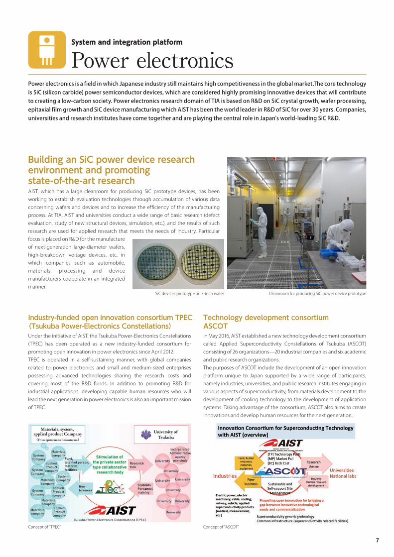
AIST, which has a large cleanroom for producing SiC prototype devices, has been working to establish evaluation technologies through accumulation of various data concerning wafers and devices and to increase the efficiency of the manufacturing process. At TIA, AIST and universities conduct a wide range of basic research (defect evaluation, study of new structural devices, simulation, etc.), and the results of such research are used for applied research that meets the needs of industry. Particular focus is placed on R&D for the manufacture of next-generation large-diameter wafers, high-breakdown voltage devices, etc. in which companies such as automobile, materials, processing and device manufacturers cooperate in an integrated manner.
Power electronics is a field in which Japanese industry still maintains high competitiveness in the global market.The core technology is SiC (silicon carbide) power semiconductor devices, which are considered highly promising innovative devices that will contribute to creating a low-carbon society. Power electronics research domain of TIA is based on R&D on SiC crystal growth, wafer processing, epitaxial film growth and SiC device manufacturing which AIST has been the world leader in R&D of SiC for over 30 years. Companies, universities and research institutes have come together and are playing the central role in Japan's world-leading SiC R&D.
Industry-funded open innovation consortium TPEC(Tsukuba Power-Electronics Constellations)
In May 2016, AIST established a new technology development consortium called Applied Superconductivity Constellations of Tsukuba (ASCOT) consisting of 26 organizations̶20 industrial companies and six academic and public research organizations.The purposes of ASCOT include the development of an open innovation platform unique to Japan supported by a wide range of participants, namely industries, universities, and public research institutes engaging in various aspects of superconductivity, from materials development to the development of cooling technology to the development of application systems. Taking advantage of the consortium, ASCOT also aims to create innovations and develop human resources for the next generation.
Technology development consortium ASCOT
Cleanroom for producing SiC power device prototypeSiC devices prototype on 3-inch wafer
Building an SiC power device research environment and promoting state-of-the-art research
8
System and integration platform
MEMS
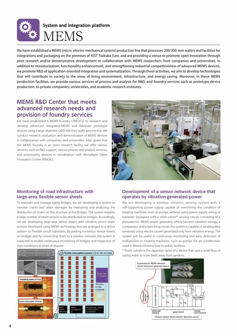
We have established a MEMS foundry (TKB-812) to research and develop advanced integrated-MEMS and fabricate prototype devices using a large-diameter (200/300 mm) wafer process line. We conduct research, evaluation and demonstration of MEMS devices in collaboration with companies and universities. Also, given that the MEMS foundry is an open research facility, we offer various services, such as R&D support, various process and analysis services, and prototyping devices in coordination with MicroNano Open Innovation Center (MNOIC).
A piezoelectric MEMS vibration sensor and power generator device
Ultralow-power ”shishi-odoshi” detection circuit
We have established a MEMS (micro-electro-mechanical system) production line that processes 200/300-mm wafers and facilities for integrations and packaging on the premises of AIST Tsukuba East, and are providing a venue to promote open innovation through joint research and/or demonstrative development in collaboration with MEMS researchers from companies and universities. In addition to miniaturization, functionality enhancement, and strengthening industrial competitiveness of advanced MEMS devices, we promote R&D of application-oriented integration and systematization. Through these activities, we aim to develop technologies that will contribute to society in the areas of living environment, infrastructure, and energy saving. Moreover, in these MEMS production facilities, we provide various services of process and analysis for R&D, and foundry services such as prototype device production, to private companies, universities, and academic research institutes.
MEMS R&D Center that meets advanced research needs and provision of foundry services
To maintain and manage aging bridges, we are developing a system to monitor cracks and other damages by measuring and analyzing the distribution of strains on the structure of the bridges. The system requires a large number of strain sensors to be distributed on bridges. Accordingly, we are developing large-area sensor sheets with ultrathin silicon strain sensors developed using MEMS technology that are arranged in a lattice pattern on flexible circuit substrates. By pasting numerous sensor sheets on bridges and by connecting them to a wireless network, the system is expected to enable continuous monitoring of bridges, and inspection of their conditions at times of disaster.
Monitoring of road infrastructure withlarge-area flexible sensor sheets
We are developing a wireless vibration sensing system with a self-supporting power supply capable of monitoring the condition of rotating machines, such as pumps, without using power supply wiring or batteries. Equipped with a shishi-odoshi* sensing circuit, consisting of a piezoelectric MEMS power generator, which harvests vibration energy, a comparator, and a switching circuit, the system is capable of sending data wirelessly using electric power generated only from vibration energy. The system will be useful in continuous monitoring and early detection of malfunction in rotating machines, such as pumps for air conditioners used in lifeline infrastructure in public facilities.* Shishi-odoshi is the Japanese name of a device that uses a small flow of spring water to scare birds away from gardens.
Development of a sensor network device thatoperates by vibration-generated power
9
In-situ observation of a solid-liquid interface using a synchrotron radiation X-ray
First-principles calculation of the interface structure
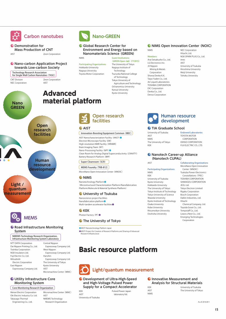
Advanced material platform
Nano-GREEN
We will identify the basic mechanisms of the surface/interface phenomena which will be the key for the function of the relevant materials by making the best use of environment controlling technology developed by NIMS.
Advanced measurement technology enabling in-situ surface/interface analysis in the operating environment
We aim to understand electron/atom dynamics at nanosurfaces/ nanointerfaces, which form the basic principle of energy conversion, using a sophisticated computational scientific method. Based on the knowledge gained from those studies, we are also drawing up guidelines for designing new materials and functions.
Computational science for dynamic analysis of electron/atom transfer, and ion diffusion, etc.
Device(Model Sample)
AdvancedCharacterizationIn-situ observation ofsurfaces and interfacesunder practicalenvironment
Computational Science
Dynamic analysisof atoms, electron migration and ion diffusion
FunctionalMaterials
Rechargeable batteries,Fuel Cells,
Photovoltaics, and Photocatalyst
Collaboration of Computation , Characterization and Materials
“Environment Cell”Small space simulating practical environments(gas, humidity, temperature, voltage etc.)
Research-framework to understand and to control materialinterfacial phenomena by coordinating and integratingmeasurements and experiments
Schematic and 10-cell stackof lithium-air battery
Schematic cross section of a low-temperaturesolution-processed perovskite solar cell and its elements
Electrontransport layer
Hole transportlayer
Transparentelectrode
Light
Perovskite layer
Electrode
LiCoO2/β-Li3PS4
4.0 2.9 1.4 3.0 eV
National Institute for Materials Science (NIMS) is playing a central role in coordination with academia, including TIA core institutes, in providing a venue for collaborative research with industries to create environmental and energy technologies using nanotechnology. We encourage a wide range of industrial partners both in Japan and abroad to participate in Nano-GREEN (Global Research Center for Environment and Energy based on Nanomaterials Science) to accelerate R&D in materials technologies. We arrange various forms of collaboration with companies according to their request. At Nano-GREEN, we aim to conduct efficient R&D through coordinated and integrated utilization of materials technologies developed by NIMS, advanced measurement technology, and computational science.
In order to develop a sustainable society, we are promoting basic R&D of materials and technologies in the areas of environment and energy. In particular, we are making major efforts for the studies on all solid-state rechargeable batteries, lithium-air rechargeable batteries, and on perovskite solar cells to address common technological issues with an all Japan formation of collaborations between industries, government and academia.
Research themes taking advantage ofNIMS-developed materials and technologies
10
Advanced material platform
Carbon nanotubes
Development of SWCNT mass production technology
O-rings fabricated from the CNT-rubber composite"Workplace environment measurement guide" and "Procedures for safety testing"http://www.aist-riss.jp/research/assessment/
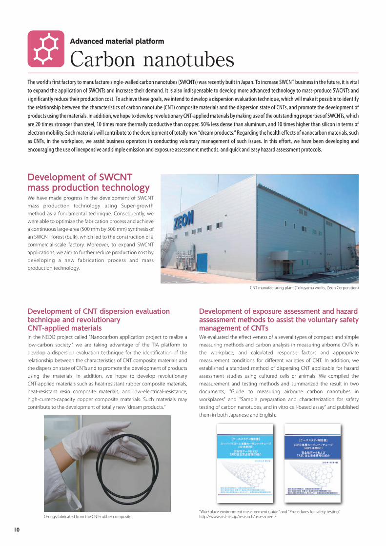
CNT manufacturing plant (Tokuyama works, Zeon Corporation)
The world’s first factory to manufacture single-walled carbon nanotubes (SWCNTs) was recently built in Japan. To increase SWCNT business in the future, it is vital to expand the application of SWCNTs and increase their demand. It is also indispensable to develop more advanced technology to mass-produce SWCNTs and significantly reduce their production cost. To achieve these goals, we intend to develop a dispersion evaluation technique, which will make it possible to identify the relationship between the characteristics of carbon nanotube (CNT) composite materials and the dispersion state of CNTs, and promote the development of products using the materials. In addition, we hope to develop revolutionary CNT-applied materials by making use of the outstanding properties of SWCNTs, which are 20 times stronger than steel, 10 times more thermally conductive than copper, 50% less dense than aluminum, and 10 times higher than silicon in terms of electron mobility. Such materials will contribute to the development of totally new “dream products.” Regarding the health effects of nanocarbon materials, such as CNTs, in the workplace, we assist business operators in conducting voluntary management of such issues. In this effort, we have been developing and encouraging the use of inexpensive and simple emission and exposure assessment methods, and quick and easy hazard assessment protocols.
We have made progress in the development of SWCNT mass production technology using Super-growth method as a fundamental technique. Consequently, we were able to optimize the fabrication process and achieve a continuous large-area (500 mm by 500 mm) synthesis of an SWCNT forest (bulk), which led to the construction of a commercial-scale factory. Moreover, to expand SWCNT applications, we aim to further reduce production cost by developing a new fabrication process and mass production technology.
In the NEDO project called "Nanocarbon application project to realize a low-carbon society," we are taking advantage of the TIA platform to develop a dispersion evaluation technique for the identification of the relationship between the characteristics of CNT composite materials and the dispersion state of CNTs and to promote the development of products using the materials. In addition, we hope to develop revolutionary CNT-applied materials such as heat-resistant rubber composite materials, heat-resistant resin composite materials, and low-electrical-resistance, high-current-capacity copper composite materials. Such materials may contribute to the development of totally new “dream products.”
Development of CNT dispersion evaluation technique and revolutionary CNT-applied materials
We evaluated the effectiveness of a several types of compact and simple measuring methods and carbon analysis in measuring airborne CNTs in the workplace, and calculated response factors and appropriate measurement conditions for different varieties of CNT. In addition, we established a standard method of dispersing CNT applicable for hazard assessment studies using cultured cells or animals. We compiled the measurement and testing methods and summarized the result in two documents, "Guide to measuring airborne carbon nanotubes in workplaces" and "Sample preparation and characterization for safety testing of carbon nanotubes, and in vitro cell-based assay" and published them in both Japanese and English.
Development of exposure assessment and hazardassessment methods to assist the voluntary safetymanagement of CNTs
11
Electrostatic ion storage ring Silicon-On-Insulator pixel detectorSuperconducting X-ray detector for X-ray absorptionfine structure spectroscopy (SC-XAFS)
Basic resource platform
Light/quantum measurement
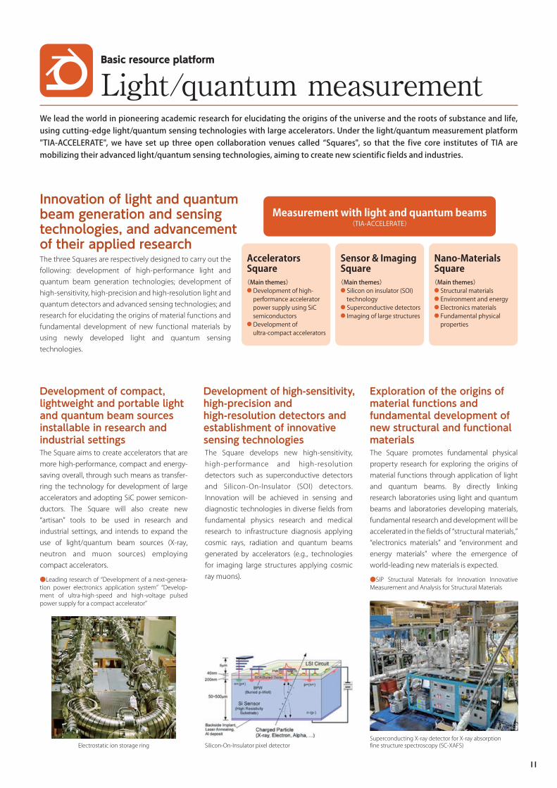
The three Squares are respectively designed to carry out the following: development of high-performance light and quantum beam generation technologies; development of high-sensitivity, high-precision and high-resolution light and quantum detectors and advanced sensing technologies; and research for elucidating the origins of material functions and fundamental development of new functional materials by using newly developed light and quantum sensing technologies.
Innovation of light and quantum beam generation and sensing technologies, and advancement of their applied research
Measurement with light and quantum beams(TIA-ACCELERATE)
Accelerators Square(Main themes)● Development of high- performance accelerator power supply using SiC semiconductors● Development of ultra-compact accelerators
Sensor & Imaging Square(Main themes)● Silicon on insulator (SOI) technology● Superconductive detectors● Imaging of large structures
Nano-Materials Square(Main themes)● Structural materials● Environment and energy● Electronics materials● Fundamental physical properties
We lead the world in pioneering academic research for elucidating the origins of the universe and the roots of substance and life, using cutting-edge light/quantum sensing technologies with large accelerators. Under the light/quantum measurement platform "TIA-ACCELERATE", we have set up three open collaboration venues called “Squares", so that the five core institutes of TIA are mobilizing their advanced light/quantum sensing technologies, aiming to create new scientific fields and industries.
The Square aims to create accelerators that are more high-performance, compact and energy- saving overall, through such means as transfer-ring the technology for development of large accelerators and adopting SiC power semicon-ductors. The Square will also create new “artisan” tools to be used in research and industrial settings, and intends to expand the use of light/quantum beam sources (X-ray, neutron and muon sources) employing compact accelerators.
●Leading research of “Development of a next-genera-tion power electronics application system” “Develop-ment of ultra-high-speed and high-voltage pulsed power supply for a compact accelerator”
Development of compact, lightweight and portable light and quantum beam sources installable in research and industrial settings
The Square develops new high-sensitivity, high-performance and high-resolution detectors such as superconductive detectors and Silicon-On-Insulator (SOI) detectors. Innovation will be achieved in sensing and diagnostic technologies in diverse fields from fundamental physics research and medical research to infrastructure diagnosis applying cosmic rays, radiation and quantum beams generated by accelerators (e.g., technologies for imaging large structures applying cosmic ray muons).
Development of high-sensitivity, high-precision and high-resolution detectors and establishment of innovative sensing technologies
The Square promotes fundamental physical property research for exploring the origins of material functions through application of light and quantum beams. By directly linking research laboratories using light and quantum beams and laboratories developing materials, fundamental research and development will be accelerated in the fields of “structural materials,” “electronics materials” and “environment and energy materials” where the emergence of world-leading new materials is expected.
●SIP Structural Materials for Innovation Innovative Measurement and Analysis for Structural Materials
Exploration of the origins of material functions and fundamental development of new structural and functional materials
12
Since graduate school education is provided through collaboration of industry, academia and government, a "TIA Graduate School power electronics course" was opened in April 2013, combining two endowed laboratories at the University of Tsukuba (the Toyota Motor-Denso power electronics endowed laboratory and the Fuji Electric power electronics endowed laboratory) and employing AIST researchers as instructors (Cooperative Graduate School System). Through systematically learning power electronics as an academic discipline and conducting collaborative research in close cooperation with company researchers, students of this course are expected to play in the future an active role in companies, and succeed and further develop Japan's advanced power electronics technologies. The human resource development undertaken in this course is implemented with the cooperation of an industry-funded consortium operated as a collaboration of industry, academia and government and based on the Tsukuba Power-Electronics Constellations (TPEC).
●Cooperative Graduate School SystemA system at the University of Tsukuba to provide education at its graduate school by employing researchers from research institutes as professors at the University of Tsukuba while keeping their status as institute researchers, and also using the research environments of those research institutes.
TIA Graduate School power electronics courseTIA̶AIST, NIMS, KEK, and University of Tsukuba̶and Kyoto University, which are centers of industry-academia-government resonance fields interaction in the area of nanotechnology, are taking charge of providing education/training to young scientists in Nanotech CUPAL. CUPAL can provide ideal research and practical training settings supplemented by cutting-edge expertise and equipment. With these resources available, CUPAL offers Nanotech Research Professional (NRP) courses, which form a joint research program aiming to foster professionals who will lead the creation of new understandings in nanotechnology. CUPAL also offers Nanotech Innovation Professional (NIP) courses, which provide basic/practical training sessions to foster professionals who will lead innovative research in nanotechnology. Furthermore researchers and students from a wide range of industries, universities, and research institutes are also able to join the NIP courses.
Nanotech Career-up Alliance: Nanotech CUPAL
Basic resource platform
Human resource development
TIA Graduate School Summer Open Festival provides students and young scientists with opportunities to gain up-to-date knowledge and skills in nanoscience/nanotechnology and to interact in an inter-organizational manner. During the event, lectures, practical training sessions, and facility tours are given by leading researchers and industrial technical experts from Japan and overseas. Students and company researchers around Japan can be qualified to participate in the event. In addition, participants can attend lectures provided in English by prestigious professors from overseas universities, and thus enjoy an international flavor in Tsukuba. Some of these educational activities are equivalent to first-term doctoral classes at the University of Tsukuba, therefore signifying the high educational quality of the event.
TIA Graduate School Summer Open Festival
https://tia-edu.jp
https://nanotechcupal.jp/nip/
We are establishing a TIA Graduate School system to develop human resources for the next generation. TIA Graduate School is educational infrastructure aiming to provide a higher level of education than any single university or research institute, taking advantage of outstanding TIA researchers and facilities. The system takes a variety of initiatives to develop skilled human resources.Nanotech Career-up Alliance (Nanotech CUPAL) is a project to foster young-generation researchers in the nanotechnology field. The project was launched in FY2014 with support from the grant-in-aid program for the development of human resources in science and technology, and is led by TIA and Kyoto University.
13
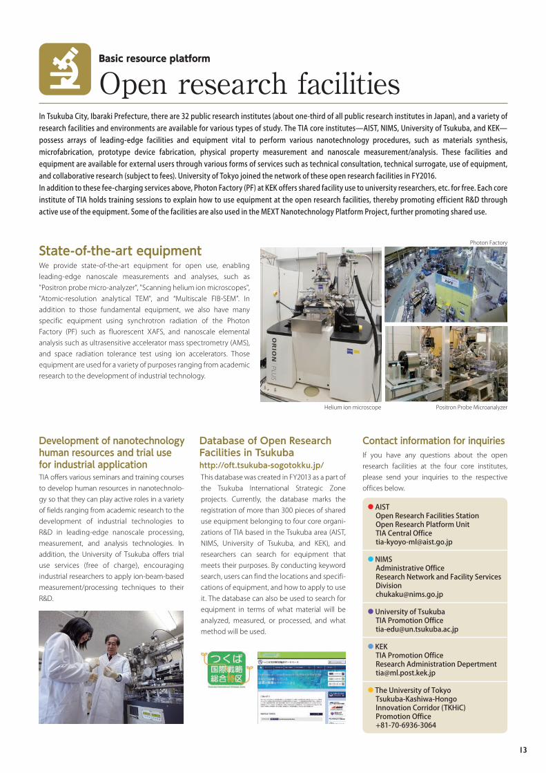
We provide state-of-the-art equipment for open use, enabling leading-edge nanoscale measurements and analyses, such as "Positron probe micro-analyzer", "Scanning helium ion microscopes", "Atomic-resolution analytical TEM", and “Multiscale FIB-SEM”. In addition to those fundamental equipment, we also have many specific equipment using synchrotron radiation of the Photon Factory (PF) such as fluorescent XAFS, and nanoscale elemental analysis such as ultrasensitive accelerator mass spectrometry (AMS), and space radiation tolerance test using ion accelerators. Those equipment are used for a variety of purposes ranging from academic research to the development of industrial technology.
State-of-the-art equipment
Basic resource platform
Open research facilities
Positron Probe Microanalyzer
Photon Factory
Helium ion microscope
● AIST Open Research Facilities Station Open Research Platform Unit TIA Central Office [email protected]
● NIMS Administrative Office Research Network and Facility Services Division [email protected]
● University of Tsukuba TIA Promotion Office [email protected]
● KEK TIA Promotion Office Research Administration Depertment [email protected]
● The University of Tokyo Tsukuba-Kashiwa-Hongo Innovation Corridor (TKHiC) Promotion Office +81-70-6936-3064
TIA offers various seminars and training courses to develop human resources in nanotechnolo-gy so that they can play active roles in a variety of fields ranging from academic research to the development of industrial technologies to R&D in leading-edge nanoscale processing, measurement, and analysis technologies. In addition, the University of Tsukuba offers trial use services (free of charge), encouraging industrial researchers to apply ion-beam-based measurement/processing techniques to their R&D.
Development of nanotechnology human resources and trial use for industrial application
This database was created in FY2013 as a part of the Tsukuba International Strategic Zone projects. Currently, the database marks the registration of more than 300 pieces of shared use equipment belonging to four core organi-zations of TIA based in the Tsukuba area (AIST, NIMS, University of Tsukuba, and KEK), and researchers can search for equipment that meets their purposes. By conducting keyword search, users can find the locations and specifi-cations of equipment, and how to apply to use it. The database can also be used to search for equipment in terms of what material will be analyzed, measured, or processed, and what method will be used.
Database of Open Research Facilities in Tsukubahttp://oft.tsukuba-sogotokku.jp/
If you have any questions about the open research facilities at the four core institutes, please send your inquiries to the respective offices below.
Contact information for inquiries
In Tsukuba City, Ibaraki Prefecture, there are 32 public research institutes (about one-third of all public research institutes in Japan), and a variety of research facilities and environments are available for various types of study. The TIA core institutes̶AIST, NIMS, University of Tsukuba, and KEK̶possess arrays of leading-edge facilities and equipment vital to perform various nanotechnology procedures, such as materials synthesis, microfabrication, prototype device fabrication, physical property measurement and nanoscale measurement/analysis. These facilities and equipment are available for external users through various forms of services such as technical consultation, technical surrogate, use of equipment, and collaborative research (subject to fees). University of Tokyo joined the network of these open research facilities in FY2016.In addition to these fee-charging services above, Photon Factory (PF) at KEK offers shared facility use to university researchers, etc. for free. Each core institute of TIA holds training sessions to explain how to use equipment at the open research facilities, thereby promoting efficient R&D through active use of the equipment. Some of the facilities are also used in the MEXT Nanotechnology Platform Project, further promoting shared use.
14
Diverse linkage in TIA
System and integration platform
Consistent research and development of next-generation SiC power electronics
AISTAsahi Diamond Industrial Co., Ltd.ULVAC, Inc.Osaka UniversityOsaka Electro-Communication UniversityCalsonic Kansei CorporationKYOCERA CorporationKyoto UniversityKOA CorporationSanken Electric Co., Ltd.JFE Techno-Research CorporationShowa Denko K.K.New Japan Radio Co.,Ltd.Sumitomo Electric Industries, Ltd.Sumitomo Bakelite Co. Ltd.TAIYO YUDEN CO., LTD.Takatori CorporationToyota Motor CorporationUniversity of TsukubaDenka Co., Ltd.Denso CorporationCentral Research Institute of Electric Power IndustryTokyo Institute of Technology
The University of TokyoTOSHIBA CORPORATIONToray Research Center, Inc.Nagoya UniversityNagoya Institute of TechnologyNISSAN MOTOR CO., LTD.NGK Insulators, Ltd.NGK Spark Plug Co., Ltd.JAPAN Fine Ceramics Co.,Ltd. NORITAKE Co., Ltd.Hitachi, Ltd.FUJI ELECTRIC CO., LTD.Fujimi IncorporatedMitsubishi Electric CorporationMEIDENSHA CORPORATIONYazaki CorporationRenesas Electronics CorporationROHM Semiconductor
Project for the Promotion to the Commercialization of High-temperature superconductivity
Participating OrganizationAISTMitsubishi Electric CorporationKyoto University
Tohoku UniversitySophia UniversityFujikura Ltd.Furukawa Electric Co., Ltd.NIMS
Applied Superconductivity Constellations of Tsukuba (ASCOT)
AISTJEOL Ltd.JECC TORISHA Co., Ltd.Suzuki Shokan Co.,Ltd.Sumitomo Heavy Industries, Ltd. Sumitomo Electric Industries, Ltd.SWCC SHOWA CABLE SYSTEMS CO.,LTD.Hitachi, Ltd.Fujikura Ltd.Fujihira Co., Ltd. Furukawa Electric Co., Ltd.MAYEKAWA MFG. CO., LTD.Mitsubishi Electric CorporationTAIYO NIPPON SANSO CORPORATION
KYUSHU ELECTRIC POWER CO. INC.Tokyo Electric Power Company Holdings, Inc.Tohoku Electric Power Co., Inc.The Kansai Electric Power Company, Inc.The Chugoku Electric Power Co.,Inc.CHUBU Electric Power Co.,Inc.Central Research Institute of Electric Power IndustryUniversity of TsukubaThe University of TokyoKyushu UniversityKyoto UniversityNIMS
Tsukuba Power Electronics Constellations (TPEC)
AISTFUJI ELECTRIC CO., LTD.ULVAC, Inc.Sumitomo Electric Industries, Ltd.Toyota Motor CorporationTOSHIBA CORPORATIONHitachi Chemical Co., Ltd.Mitsubishi Electric CorporationRigaku CorporationKomatsu Ltd.OMRON CorporationTokyo Electron LimitedKeysight Technologies Japan G.K.Keysight Technologies International Japan G.K.ACR Co.,LtdADEKA CORPORATIONESPEC Corp.Oita Device Technology Co.,LtdCATS Inc.KYOCERA CorporationSankei Engineering Co., LtdJFE Steel CorporationTDK Corporation
TESEC CorporationTOKYO SEIMITSU CO., LTDToray Industries, Inc.JEOL Ltd.Pulsed Power Japan laboratory ltd.NISSIN ELECTRIC Co.,Ltd.Central Research Institute of Electric Power IndustryUniversity of TsukubaKyoto UniversityOsaka UniversityTokyo Institute of TechnologyKEKNIMSIwate UniversityNagaoka University of TechnologyOsaka Institute of TechnologyKeio UniversityRIKENSaitama UniversityQST
Measurement/Evaluation Technologies for Advanced Functional Materials & Measurement/Evaluation technologies for nano-defect inspectionEvolving nano process Infrastructure Development Center, Inc. (EIDEC)
StockholdersDai Nippon Printing Co., Ltd.FUJIFILM CorporationJSR CorporationNIKON CorporationShin-Etsu Chemical Co., Ltd.Tokyo Electron LimitedToshiba Corporation
Joint or Committed R&DIntel CorporationKyoto UniversityOsaka UniversityTokyo Institute of TechnologyTokyo Ohka Kogyo Co., Ltd.HORIBA STEC, Co., Ltd.RION Co., Ltd.NIMSAIST
Vertically Integrated Center for Technologies of Optical Routing toward Ideal Energy Savings
AIST
Collaborating CompaniesNIPPON TELEGRAPH AND TELEPHONE CORPORATIONFUJITSU LABORATORIES LTD.Furukawa Electric Co., Ltd.Trimatiz LimitedNEC CorporationFujitsu Limited
Fujikura Ltd.Alnair Labs CorporationSumitomo Electric Industries, Ltd.KITANIHON ELECTRIC CABLE CO., LTD.
Minimal FabMinimal Fab Deveropment Assosiation
Collaborating CompaniesPRE-TECH CO.,LTD.Litho Tech Japan CorporationSANMEI CorporationPMT CORPORATIONFujikoshi Machinery Corp.Fuji Imvac Inc,SAKAGUCHI E.H VOC CORP.Aichi System Co.,Ltd.TAZMO CO.,LTD.Fujikin IncorporatedHORIBA, Ltd.Design NetworkSanyo Co., Ltd.Taisei CorporationLogic Research
TOOL CorporationYokogawa Solution Service CorporationYONEKURA MFG. Co., LTD.Koyo Thermo Systems Co.,Ltd.KATAGIRI ENGINIEERING CO.,LTD.seinan indusutries Co.,LtdSPP Technologies Co., Ltd.
R&D Project for the Next Generation Smart Device
Denso CorporationLAPIS Semiconductor Co., Ltd.AISTToyota Central R&D Labs., Inc.
Zuken Inc.Sumitomo Precision Products Co., Ltd.
Cross-sectional R&D Project for IoT Promotion (R&D Project for High-Speed/High-Density Storage Device & Systems)
Member CompaniesTOSHIBA CORPORATIONEBARA CORPORATIONTokyo Electron Limited
Joint or Committed R&DAISTNagoya UniversityKeio UniversityShibaura Institute of TechnologyTokyo Polytechnic University
Development of One Million LUT Atom Switch FPGA
Member CompaniesNEC Corporation
Joint or Committed R&DRitsumeikan UniversityAIST
Achieving Ultimate Green IT Devices with Long Usage Time without Charging
AISTToshiba Corporation
Fujitsu Limited
Integrated Photonics-Electronics Convergence System TechnologyPhotonics Electronics Technology Research Association (PETRA)
Participating OrganizationNEC CorporationFujitsu LimitedOki Electric Industry Co., Ltd.TOSHIBA CORPORATIONFurukawa Electric Co., Ltd.NIPPON TELEGRAPH AND TELEPHONE CORPORATIONNTT Electronics CorporationAIST
Optoelectronics Industry and Technology Development Association (OITDA)
Joint ResearchThe University of TokyoYokohama National UniversityKyoto UniversityTokyo Institute of TechnologyWaseda University
Nanoelectronics
Power electronics
CNT
Nano-electronics
Powerelectronics
MEMS
15
Basic resource platform
Advanced material platform
Road Infrastructure Monitoring SystemNMEMS Technology Research Organization, Infrastructure Monitoring System Laboratory
NTT DATA CorporationDai Nippon Printing Co., Ltd.Toshiba CorporationNGK Insulators Ltd.Fuji Electric Co. Ltd.Mitsubishi Electric CorporationEast Nippon Expressway Company Ltd.
Central Nippon Expressway Company Ltd.West Nippon Expressway Company Ltd.Hanshin Expressway Company Ltd.The University of TokyoKyoto UniversityAISTMicromachine Center (MMC)
Utility Infrastructure Core Monitoring SystemCore Monitoring Research Organization
Meisei Electric CorporationOki Electric Industry Co. Ltd.Takasago Thermal Engineering Co., Ltd.
Micromachine Center (MMC)AISTNMEMS Technology Research Organization
Innovative Measurement and Analysis for Structural Materials
KEKAISTNIMS
University of TsukubaThe University of Tokyo
Development of Ultra-High-Speed and High-Voltage Pulsed Power Supply for a Compact Accelerator
KEKAISTUniversity of Tsukuba
Pulsed Power Japan laboratory ltd.
Demonstration for Mass Production of CNT
AIST Zeon Corporation
Nano-carbon Application Project towards Low-carbon SocietyTechnology Research Associationfor Single Wall Carbon Nanotubes (TASC)
CNT DivisionNEC Corporation
Zeon CorporationAIST
Carbon nanotubes
Global Research Center for Environment and Energy based on Nanomaterials Science (GREEN)
NIMS
Participating OrganizationsHokkaido UniversityNagoya UniversityToyota Motor Corporation
Guest Institutions 〈GREEN Open-lab〉 (FY2015)The University of TokyoNagoya Institute of TechnologyTsuruoka National College of TechnologyTokyo University of Agriculture and TechnologyOchanomizu UniversityKansai UniversityKyoto University
NIMS Open Innovation Center (NOIC)NIMS
MembersArai Seisakusho Co., Ltd. LG Electronics Inc.JX Nippon Mining & Metals CorporationShowa Denko K.K.Taiyo Yuden Co., Ltd.Air Liquid LaboratoriesTOSHIBA CORPORATIONDIC CorporationDenka Co., Ltd.Denso Corporation
NEC CorporationHitachi, Ltd.NGK SPARK PLUG Co., Ltd.imecAISTUniversity of TsukubaHiroshima UniversityMeiji UniversityTohoku University
Nano-GREEN
AISTInnovation-Boosting Equipment Common (IBEC)
Super Cleanroom (SCR)
MEMS Foundry (TKB-812)
AIST Nanocharacterization Facility (ANCF)●Electron Microscope Facility (EM)High-resolution NMR Facility (HRNMR)Brain Imaging Team (BIT)Nano-Processing Facility (NPF)●Clean Room for Analog-Digital Superconductivity (CRAVITY) Battery Research Platform (BRP)
MicroNano Open Innovation Center (MNOIC)
NIMSNanotechnology Platform●(Microstructural Characterization Platform/Nanofabrication Platform/Molecule & Material Synthesis Platform)
University of TsukubaNanoscience project facilitiesNanofabrication platform●Multi-tandem accelerator facilities●
KEKPhoton Factory (PF)●
The University of Tokyo
●MEXT-Nanotechnology Platform Japan
●MEXT-Project for Creation of Research Platforms and Sharing of Advanced Research Infrastructure
Open research facilities
MEMS
Light/quantum measurement
TIA Graduate SchoolUniversity of TsukubaAISTNIMSThe University of TokyoKEK
Endowed LaboratoriesTOYOTA MOTOR CORPORATIONDENSO CORPORATIONFUJI ELECTRIC CO., LTD.
Nanotech Career-up Alliance(Nanotech CUPAL)
AIST
Participating OrganizationsNIMSKEKUniversity of TsukubaKyoto UniversityHokkaido UniversityThe University of TokyoTokyo Institute of TechnologyTokyo University of ScienceWaseda UniversityKyoto Institute of TechnologyOsaka UniversityKobe UniversityRitsumeikan UniversityDoshisha University
Collaborating OrganizationsMicroNano Open Innovation Center (MNOIC)Tsukuba Power-Electronics Constellations (TPEC)TOSHIBA CORPORATIONSHIMADZU CORPORATIONJEOL Ltd.Tokyo Electron LimitedRigaku CorporationBosch CorporationDaikin Industries, Ltd.Hitachi Chemical Company, Ltd.Toyoda Gosei Co., Ltd.Tempstaff Co., Ltd.Leave a Nest Co., Ltd.Emerging Technologies Corporation
Human resource development
NanoGREEN
Openresearchfacilities
Humanresource
development
Light /quantum
measurement
As of 2016/8/1
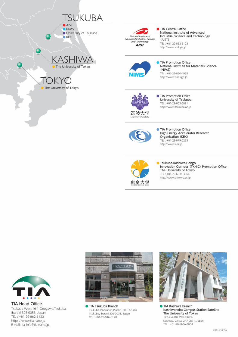
TOKYOThe University of Tokyo
KASHIWAThe University of Tokyo
TSUKUBAAISTNIMSUniversity of TsukubaKEK
TIA Head OfficeTsukuba West,16-1 Onogawa,TsukubaIbaraki 305-0053, JapanTEL : +81-29-862-6123https://www.tia-nano.jpE-mail: [email protected]
©2016.10 TIA
TIA Tsukuba BranchTsukuba Innovation Plaza,1-10-1 AzumaTsukuba, Ibaraki 305-0031, JapanTEL : +81-29-846-6120
TIA Kashiwa BranchKashiwanoha Campus Station SatelliteThe University of Tokyo178-4-4-207 Wakashiba, Kashiwa, Chiba, 277-0871, JapanTEL : +81-70-6936-3064
TIA Central OfficeNational Institute of AdvancedIndustrial Science and Technology(AIST)TEL : +81-29-862-6123http://www.aist.go.jp
TIA Promotion OfficeNational Institute for Materials Science (NIMS)TEL : +81-29-860-4955http://www.nims.go.jp
TIA Promotion OfficeUniversity of TsukubaTEL : +81-29-853-5891http://www.tsukuba.ac.jp
TIA Promotion OfficeHigh Energy Accelerator ResearchOrganization (KEK)TEL : +81-29-879-6253http://www.kek.jp
Tsukuba-Kashiwa-Hongo Innovation Corridor (TKHiC) Promotion Office The University of TokyoTEL : +81-70-6936-3064http://www.u-tokyo.ac.jp


![Policy innovation platform [draft!]](https://img.pdfslide.us/doc/110x75/587fe9f01a28ab46228b60c9/policy-innovation-platform-draft.jpg)