Embed Size (px)
Citation preview
International Research Journal of Engineering and Technology (IRJET) e-ISSN: 2395 -0056
Volume: 03 Issue: 03 | Mar-2016 www.irjet.net p-ISSN: 2395-0072
© 2016, IRJET | Impact Factor value: 4.45 | ISO 9001:2008 Certified Journal | Page 1256
A Novel Transformer-less Voltage Quadruple with Low Switch Voltage Stress Solar DC-DC Converter by Using Fuzzy Logic
Controller
JEBA ASAM1 TIKESHWAR GAJPAL2
([email protected]) ([email protected])
M.E. Scholar (Power electronics) 1
Assistant Proffesor2
Raipur institute of technology, Raipur (C.G.) ABSTRACT - In this paper, a novel transformer-less adjustable voltage quadruple solar dc–dc converter with high-
voltage transfer gain and reduced value of settling time & semiconductor voltage stress by using (FLC) fuzzy logic
controller is proposed. The proposed topology utilizes input-parallel output-series configuration for providing a
much higher voltage gain. The proposed converter cannot only achieve high step-up voltage gain with reduced
component count but also reduce the voltage stress of both active switches and diodes. This will allow one to
choose lower voltage rating MOSFETs and diodes to reduce both switching and conduction losses. In addition, due
to the charge balance of the blocking capacitor ,the features of converter provides automatic uniform current
sharing characteristic of the two interleaved phases without adding extra circuitry or complex control methods. By
using fuzzy logic controller the output voltage of the proposed converter can improve with reducing the settling
time. The output part is connected to the PMSM through which we can calculate stator current & rotor speed of the
machine & uses in many applications. The operation principle and steady analysis as well as a comparison with
other recent existing high step-up topologies are presented. Finally, some simulation and experimental results are
also presented to demonstrate the effectiveness of the proposed converter.
Keywords- dc-dc, MOSFET, FLC
INTRODUCTION
Power Electronics is the art of converting electrical energy from one form to another in an efficient, clean,
compact, and robust manner for convenient utilization. A passenger lift in a modern building equipped with a
Variable-Voltage-Variable-Speed induction-machine drive offers a comfortable ride and stops exactly at the floor
level. Behind the scene it consumes less power with reduced stresses on the motor and corruption of the utility
mains.
International Research Journal of Engineering and Technology (IRJET) e-ISSN: 2395 -0056
Volume: 03 Issue: 03 | Mar-2016 www.irjet.net p-ISSN: 2395-0072
© 2016, IRJET | Impact Factor value: 4.45 | ISO 9001:2008 Certified Journal | Page 1257
Power Electronics involves the study of
• Power semiconductor devices - their physics, characteristics, drive requirements and their protection for
optimum utilization of their capacities,
• Power converter topologies involving them,
• Control strategies of the converters,
• Digital, analogue and microelectronics involved,
• Capacitive and magnetic energy storage elements,
• Rotating and static electrical devices,
• Quality of waveforms generated,
• Electro Magnetic and Radio Frequency Interference
Power electronic converters - To modify the form of electrical energy (voltage, current or frequency).
Power range - from some mille watts (mobile phone) to hundreds of megawatts (HVDC transmission system). With
"classical" electronics, electrical currents and voltage are used to carry information, whereas with power
electronics, they carry power. Thus, the main metric of power electronics becomes the efficiency.
The first very high power electronic devices were mercury arc valves. In modern systems the conversion is
performed with semiconductor switching devices such as diodes, thyristors and transistors. In contrast to
electronic systems concerned with transmission and processing of signals and data, in power electronics
substantial amounts of electrical energy are processed.
An AC/DC converter (rectifier) is the most typical power electronics device found in many consumer electronic
devices, e.g., television sets, personal computers, battery chargers, etc. The power range is typically from tens
of watts to several hundred watts. In industry the most common application is the variable speed drive that is
used to control an induction motor. The power range of VSDs start from a few hundred watts and end at tens
of megawatts.
The power conversion systems can be classified according to the type of the input and output power
• AC to DC (rectification)
• DC to AC (inversion)
• DC to DC (chopping)
International Research Journal of Engineering and Technology (IRJET) e-ISSN: 2395 -0056
Volume: 03 Issue: 03 | Mar-2016 www.irjet.net p-ISSN: 2395-0072
© 2016, IRJET | Impact Factor value: 4.45 | ISO 9001:2008 Certified Journal | Page 1258
• AC to AC (transformation)
A dc–dc fly back converter is a very simple isolated structure with a high step-up voltage gain, but the active switch
of this converter will suffer a high voltage stress due to the leakage inductance of the transformer. So this type of
dc–dc converter with high-voltage transfer gain and reduced semiconductor voltage stress is proposed. The
proposed topology utilizes input-parallel output-series configuration for providing a much higher voltage gain
without adopting an extreme large duty cycle. This converter cannot only achieve high step-up voltage gain with
reduced component count but also reduce the voltage stress of both active switches and diodes. This will allow one
to choose lower voltage rating MOSFETs and diodes to reduce both switching and conduction losses .In addition,
due to the charge balance of the blocking capacitor, the converter features automatic uniform current sharing
characteristic of the two interleaved phases for voltage boosting mode without adding extra circuitry or complex
control methods.
CONVENTIONAL METHOD:
The conventional switched capacitor technique makes the switch suffer high transient current and large
conduction losses. Furthermore, many switched capacitor cells are required to obtain extremely high step-up
conversion, which increases the circuit complexity. The authors presented some design rules useful for developing
high-efficiency switched-capacitor converters, based on their analysis. several modular converter topologies were
presented based on a switched-capacitor cell concept in which a soft-switched scheme was used to reduce the
switching loss and electromagnetic interference. The coupled inductor-based converters are another solution to
implement high step-up gain because the turns ratio of the coupled inductor can be employed as another control
freedom to extend the voltage gain. However, the input current ripple is relatively larger by employing single stage
single-phase-coupled inductor-based converters, which may shorten the usage life of the input electrolytic
capacitor.
DRAWBACKS:
• High transient current and large conduction losses.
• Current ripple is high.
• Voltage stress is high.
• Low output voltage.
International Research Journal of Engineering and Technology (IRJET) e-ISSN: 2395 -0056
Volume: 03 Issue: 03 | Mar-2016 www.irjet.net p-ISSN: 2395-0072
© 2016, IRJET | Impact Factor value: 4.45 | ISO 9001:2008 Certified Journal | Page 1259
• High settling time.
PROPOSED METHOD:
A novel transformer-less adjustable voltage quadruple solar–dc converter with high voltage transfer gain and
reduced settling time & semiconductor voltage stress by using fuzzy logic controller is proposed. The proposed
topology utilizes input-parallel output-series configuration and is derived from a two-phase interleaved boost
converter for providing a much higher voltage gain with low settling time and without adopting an extreme large
duty cycle. The proposed converter cannot only achieve high step-up voltage gain but also reduce the voltage
stress of both active switches and diodes. This will allow one to choose lower voltage rating MOSFETs and diodes
to reduce both switching and conduction losses. In addition, due to the charge balance of the blocking capacitor,
the converter features automatic uniform current sharing characteristic of the two interleaved phases for voltage
boosting mode without adding any extra circuitry or complex control methods. In the output side an inverter is
connected which converts the dc output to the ac, this ac signal is provided to the PMSM (Permanent magnet
synchronous machine) for application purpose through which we can calculate stator current, torque etc. of the
motor.
OPERATING PRINCIPLE:
The instantaneous dissipated power of a device P = V.I
Thus, losses of a power device are at a minimum when the voltage across it is zero (the device is in the On-State) or
when no current flows through it (Off-State). Therefore, a power electronic converter is built around one (or more)
device operating in switching mode (either On or Off).
DC SUPPLY:
Dc supply-A power supply is an electronic device that supplies electric energy to an electrical load.
The primary function of a power supply is to convert one form of electrical energy to another and, as a
result, power supplies are sometimes referred to as electric power converters.
Some power supplies are discrete, stand-alone devices, whereas others are built into larger devices along
with their loads.
Examples of the latter include power supplies found in desktop computers and consumer
electronics devices.
International Research Journal of Engineering and Technology (IRJET) e-ISSN: 2395 -0056
Volume: 03 Issue: 03 | Mar-2016 www.irjet.net p-ISSN: 2395-0072
© 2016, IRJET | Impact Factor value: 4.45 | ISO 9001:2008 Certified Journal | Page 1260
High precision Programmable DC Power Supplies are commonly used in DC-DC converter, PV inverter,
telecom, battery chargers, With power ranges from 600W to 15kW and constant power operating envelope,
current range up to 160A.
VOLTAGE QUADRUPLE CONVERTER:
Voltage quadruple is nothing but a voltage multiplier it would produces output voltage four times of input.
A voltage multiplier is an electrical circuit that converts AC electrical power from a lower voltage to a
higher DC voltage, typically using a network of capacitors and diodes.
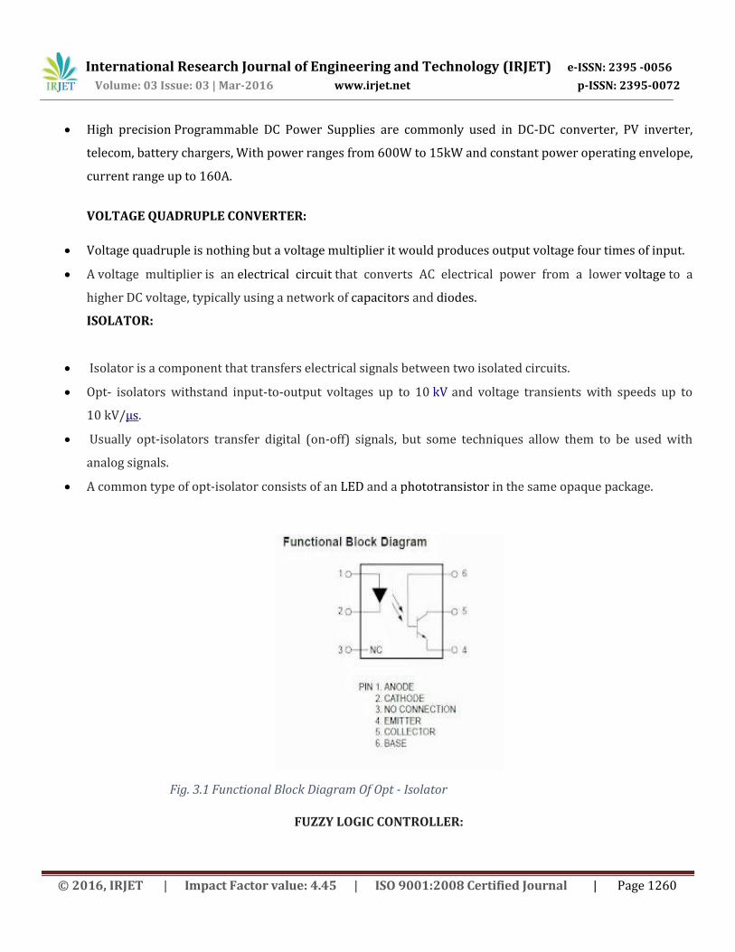
ISOLATOR:
Isolator is a component that transfers electrical signals between two isolated circuits.
Opt- isolators withstand input-to-output voltages up to 10 kV and voltage transients with speeds up to
10 kV/μs.
Usually opt-isolators transfer digital (on-off) signals, but some techniques allow them to be used with
analog signals.
A common type of opt-isolator consists of an LED and a phototransistor in the same opaque package.
Fig. 3.1 Functional Block Diagram Of Opt - Isolator
FUZZY LOGIC CONTROLLER:
International Research Journal of Engineering and Technology (IRJET) e-ISSN: 2395 -0056
Volume: 03 Issue: 03 | Mar-2016 www.irjet.net p-ISSN: 2395-0072
© 2016, IRJET | Impact Factor value: 4.45 | ISO 9001:2008 Certified Journal | Page 1261
Fuzzy logic was first proposed by Lotfi A. Zadeh of the University of California at Berkeley in a 1965 paper. Fuzzy systems were initially implemented in Japan.
Work on fuzzy systems is also proceeding in the United State and Europe, although on a less extensive
scale than in Japan.
Fuzzy logic is widely used in machine control. The term "fuzzy" refers to the fact that the logic involved can deal with concepts that cannot be expressed as the "true" or "false" but rather as "partially true"
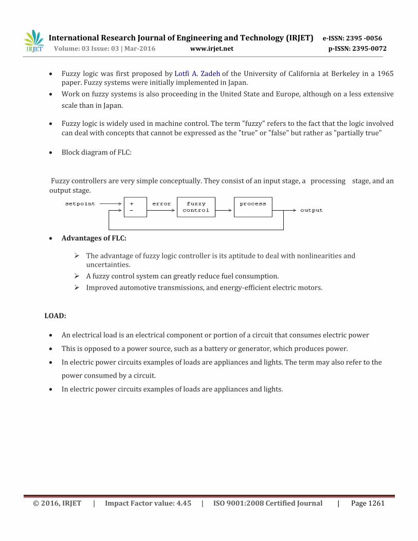
Block diagram of FLC:
Fuzzy controllers are very simple conceptually. They consist of an input stage, a processing stage, and an
output stage.
Advantages of FLC:
The advantage of fuzzy logic controller is its aptitude to deal with nonlinearities and
uncertainties.
A fuzzy control system can greatly reduce fuel consumption.
Improved automotive transmissions, and energy-efficient electric motors.
LOAD:
An electrical load is an electrical component or portion of a circuit that consumes electric power
This is opposed to a power source, such as a battery or generator, which produces power.
In electric power circuits examples of loads are appliances and lights. The term may also refer to the
power consumed by a circuit.
In electric power circuits examples of loads are appliances and lights.
International Research Journal of Engineering and Technology (IRJET) e-ISSN: 2395 -0056
Volume: 03 Issue: 03 | Mar-2016 www.irjet.net p-ISSN: 2395-0072
© 2016, IRJET | Impact Factor value: 4.45 | ISO 9001:2008 Certified Journal | Page 1262
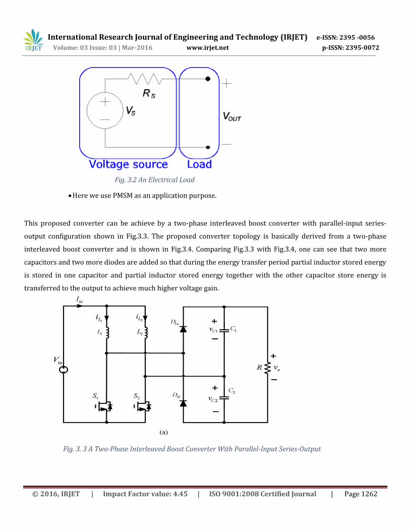
Fig. 3.2 An Electrical Load
Here we use PMSM as an application purpose.
This proposed converter can be achieve by a two-phase interleaved boost converter with parallel-input series-
output configuration shown in Fig.3.3. The proposed converter topology is basically derived from a two-phase
interleaved boost converter and is shown in Fig.3.4. Comparing Fig.3.3 with Fig.3.4, one can see that two more
capacitors and two more diodes are added so that during the energy transfer period partial inductor stored energy
is stored in one capacitor and partial inductor stored energy together with the other capacitor store energy is
transferred to the output to achieve much higher voltage gain.
Fig. 3. 3 A Two-Phase Interleaved Boost Converter With Parallel-Input Series-Output
International Research Journal of Engineering and Technology (IRJET) e-ISSN: 2395 -0056
Volume: 03 Issue: 03 | Mar-2016 www.irjet.net p-ISSN: 2395-0072
© 2016, IRJET | Impact Factor value: 4.45 | ISO 9001:2008 Certified Journal | Page 1263
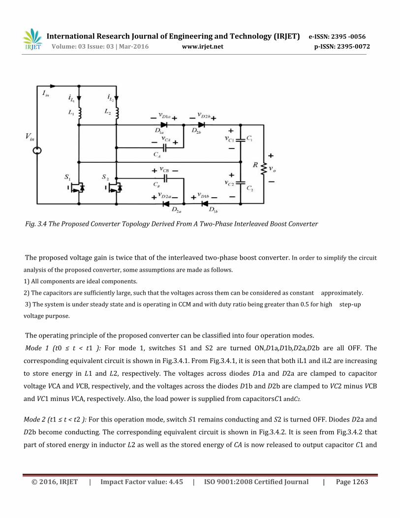
Fig. 3.4 The Proposed Converter Topology Derived From A Two-Phase Interleaved Boost Converter
The proposed voltage gain is twice that of the interleaved two-phase boost converter. In order to simplify the circuit
analysis of the proposed converter, some assumptions are made as follows.
1) All components are ideal components.
2) The capacitors are sufficiently large, such that the voltages across them can be considered as constant approximately.
3) The system is under steady state and is operating in CCM and with duty ratio being greater than 0.5 for high step-up
voltage purpose.
The operating principle of the proposed converter can be classified into four operation modes.
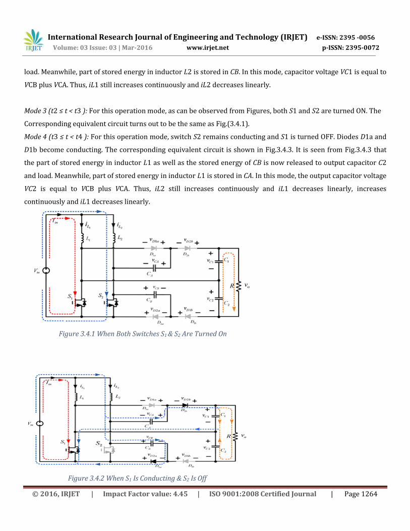
Mode 1 (t0 ≤ t < t1 ): For mode 1, switches S1 and S2 are turned ON,D1a,D1b,D2a,D2b are all OFF. The
corresponding equivalent circuit is shown in Fig.3.4.1. From Fig.3.4.1, it is seen that both iL1 and iL2 are increasing
to store energy in L1 and L2, respectively. The voltages across diodes D1a and D2a are clamped to capacitor
voltage VCA and VCB, respectively, and the voltages across the diodes D1b and D2b are clamped to VC2 minus VCB
and VC1 minus VCA, respectively. Also, the load power is supplied from capacitorsC1 andC2.
Mode 2 (t1 ≤ t < t2 ): For this operation mode, switch S1 remains conducting and S2 is turned OFF. Diodes D2a and
D2b become conducting. The corresponding equivalent circuit is shown in Fig.3.4.2. It is seen from Fig.3.4.2 that
part of stored energy in inductor L2 as well as the stored energy of CA is now released to output capacitor C1 and
International Research Journal of Engineering and Technology (IRJET) e-ISSN: 2395 -0056
Volume: 03 Issue: 03 | Mar-2016 www.irjet.net p-ISSN: 2395-0072
© 2016, IRJET | Impact Factor value: 4.45 | ISO 9001:2008 Certified Journal | Page 1264
load. Meanwhile, part of stored energy in inductor L2 is stored in CB. In this mode, capacitor voltage VC1 is equal to
VCB plus VCA. Thus, iL1 still increases continuously and iL2 decreases linearly.
Mode 3 (t2 ≤ t < t3 ): For this operation mode, as can be observed from Figures, both S1 and S2 are turned ON. The
Corresponding equivalent circuit turns out to be the same as Fig.(3.4.1).
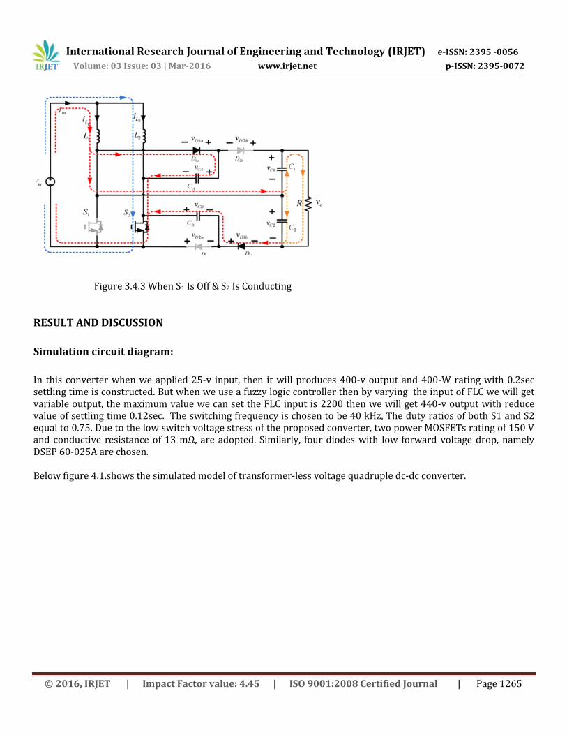
Mode 4 (t3 ≤ t < t4 ): For this operation mode, switch S2 remains conducting and S1 is turned OFF. Diodes D1a and
D1b become conducting. The corresponding equivalent circuit is shown in Fig.3.4.3. It is seen from Fig.3.4.3 that
the part of stored energy in inductor L1 as well as the stored energy of CB is now released to output capacitor C2
and load. Meanwhile, part of stored energy in inductor L1 is stored in CA. In this mode, the output capacitor voltage
VC2 is equal to VCB plus VCA. Thus, iL2 still increases continuously and iL1 decreases linearly, increases
continuously and iL1 decreases linearly.
Figure 3.4.1 When Both Switches S1 & S2 Are Turned On
Figure 3.4.2 When S1 Is Conducting & S2 Is Off
International Research Journal of Engineering and Technology (IRJET) e-ISSN: 2395 -0056
Volume: 03 Issue: 03 | Mar-2016 www.irjet.net p-ISSN: 2395-0072
© 2016, IRJET | Impact Factor value: 4.45 | ISO 9001:2008 Certified Journal | Page 1265
Figure 3.4.3 When S1 Is Off & S2 Is Conducting
RESULT AND DISCUSSION
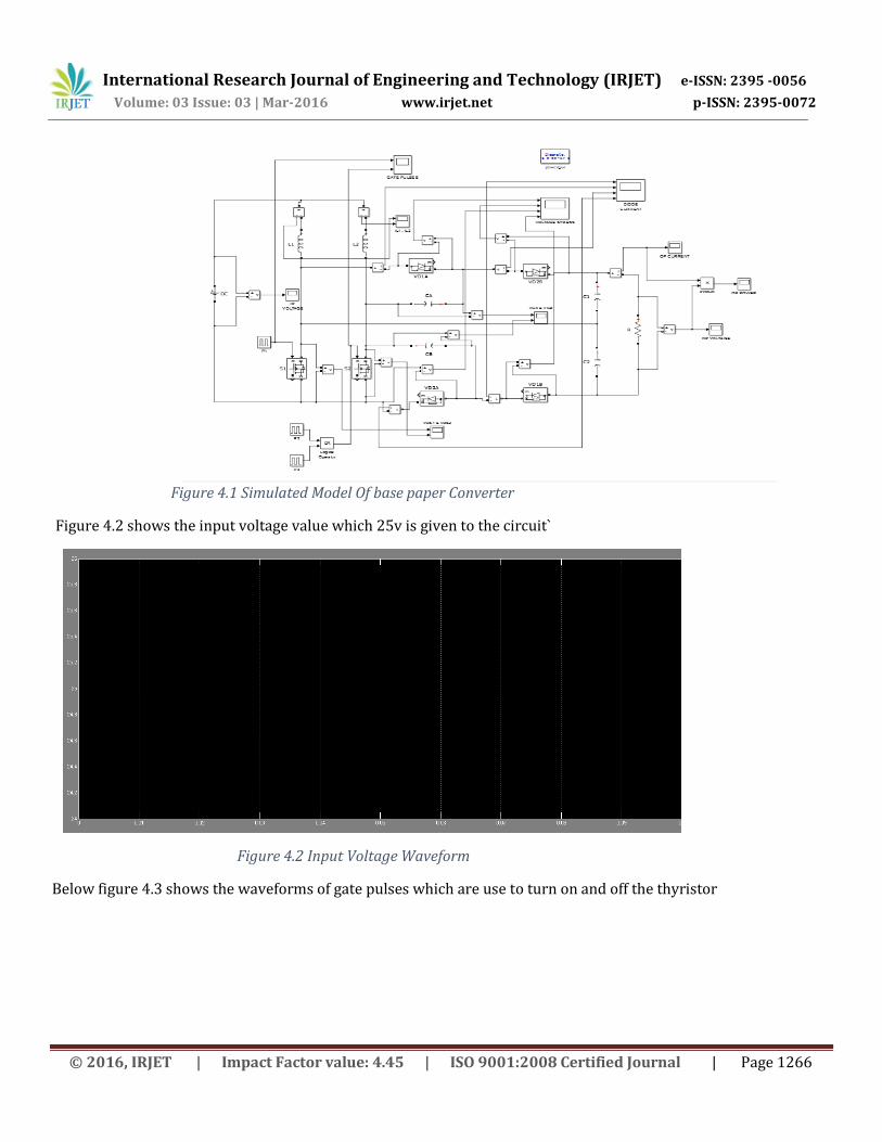
Simulation circuit diagram:
In this converter when we applied 25-v input, then it will produces 400-v output and 400-W rating with 0.2sec settling time is constructed. But when we use a fuzzy logic controller then by varying the input of FLC we will get variable output, the maximum value we can set the FLC input is 2200 then we will get 440-v output with reduce value of settling time 0.12sec. The switching frequency is chosen to be 40 kHz, The duty ratios of both S1 and S2 equal to 0.75. Due to the low switch voltage stress of the proposed converter, two power MOSFETs rating of 150 V and conductive resistance of 13 mΩ, are adopted. Similarly, four diodes with low forward voltage drop, namely DSEP 60-025A are chosen.
Below figure 4.1.shows the simulated model of transformer-less voltage quadruple dc-dc converter.
International Research Journal of Engineering and Technology (IRJET) e-ISSN: 2395 -0056
Volume: 03 Issue: 03 | Mar-2016 www.irjet.net p-ISSN: 2395-0072
© 2016, IRJET | Impact Factor value: 4.45 | ISO 9001:2008 Certified Journal | Page 1266
Figure 4.1 Simulated Model Of base paper Converter
Figure 4.2 shows the input voltage value which 25v is given to the circuit`
Figure 4.2 Input Voltage Waveform
Below figure 4.3 shows the waveforms of gate pulses which are use to turn on and off the thyristor
International Research Journal of Engineering and Technology (IRJET) e-ISSN: 2395 -0056
Volume: 03 Issue: 03 | Mar-2016 www.irjet.net p-ISSN: 2395-0072
© 2016, IRJET | Impact Factor value: 4.45 | ISO 9001:2008 Certified Journal | Page 1267
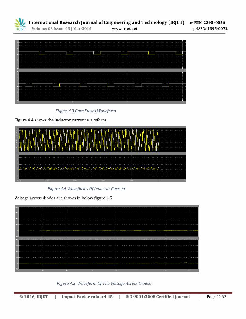
Figure 4.3 Gate Pulses Waveform
Figure 4.4 shows the inductor current waveform
Figure 4.4 Waveforms Of Inductor Current
Voltage across diodes are shown in below figure 4.5
Figure 4.5 Waveform Of The Voltage Across Diodes
International Research Journal of Engineering and Technology (IRJET) e-ISSN: 2395 -0056
Volume: 03 Issue: 03 | Mar-2016 www.irjet.net p-ISSN: 2395-0072
© 2016, IRJET | Impact Factor value: 4.45 | ISO 9001:2008 Certified Journal | Page 1268
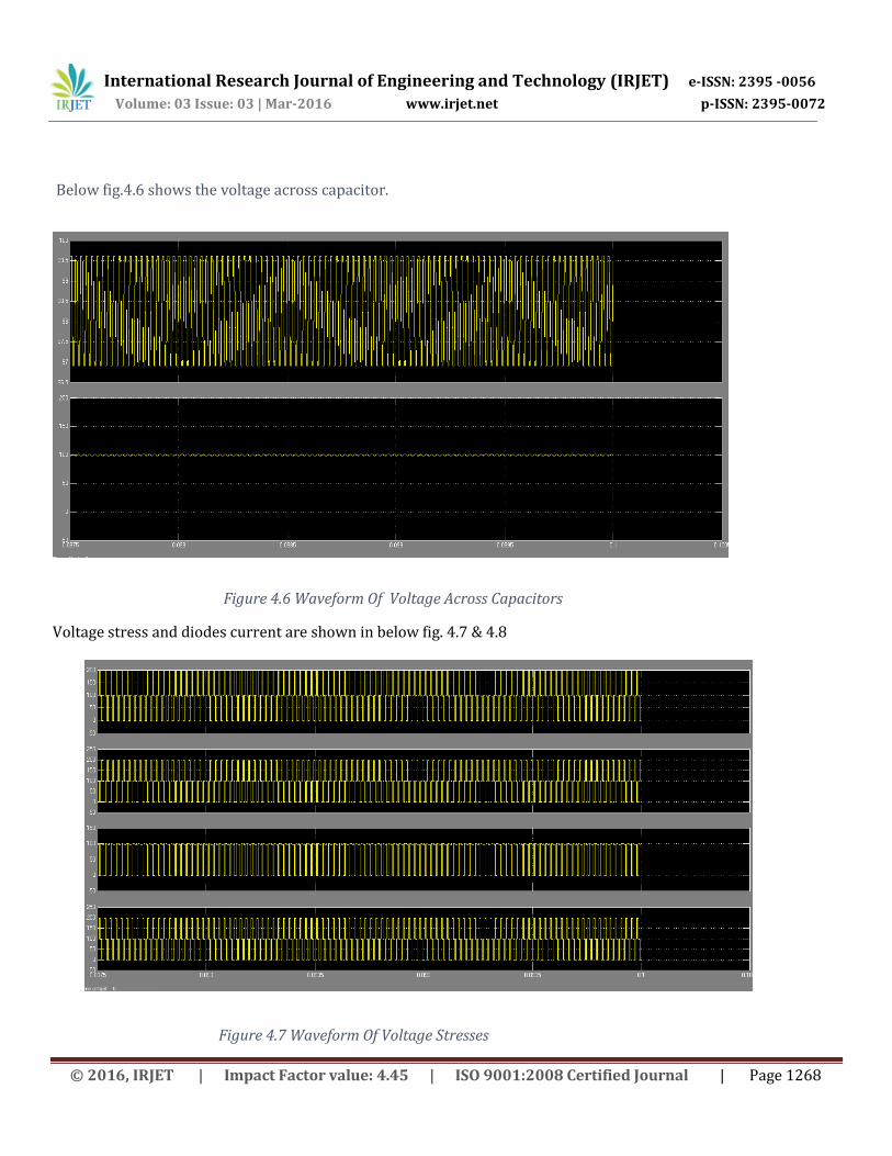
Below fig.4.6 shows the voltage across capacitor.
Figure 4.6 Waveform Of Voltage Across Capacitors
Voltage stress and diodes current are shown in below fig. 4.7 & 4.8
Figure 4.7 Waveform Of Voltage Stresses
International Research Journal of Engineering and Technology (IRJET) e-ISSN: 2395 -0056
Volume: 03 Issue: 03 | Mar-2016 www.irjet.net p-ISSN: 2395-0072
© 2016, IRJET | Impact Factor value: 4.45 | ISO 9001:2008 Certified Journal | Page 1269
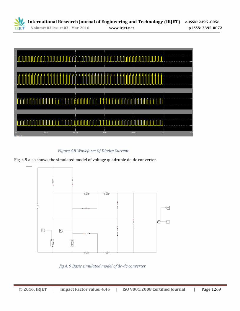
Figure 4.8 Waveform Of Diodes Current
Fig. 4.9 also shows the simulated model of voltage quadruple dc-dc converter.
fig.4. 9 Basic simulated model of dc-dc converter
International Research Journal of Engineering and Technology (IRJET) e-ISSN: 2395 -0056
Volume: 03 Issue: 03 | Mar-2016 www.irjet.net p-ISSN: 2395-0072
© 2016, IRJET | Impact Factor value: 4.45 | ISO 9001:2008 Certified Journal | Page 1270
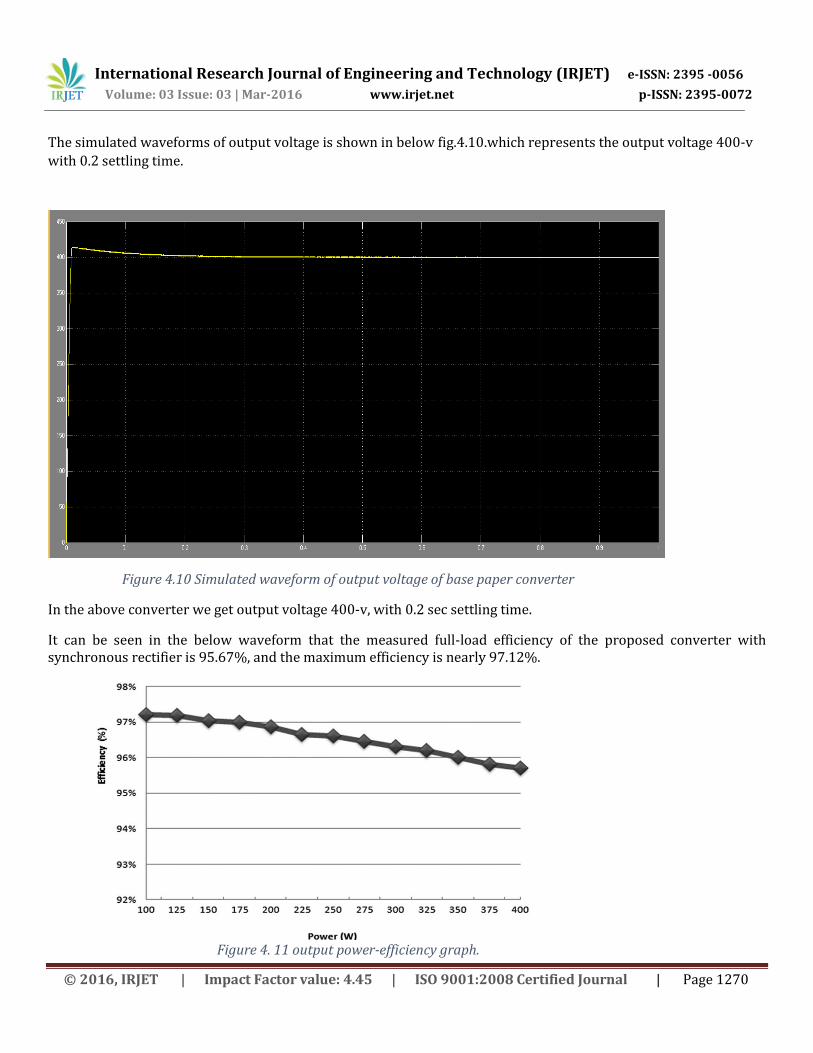
The simulated waveforms of output voltage is shown in below fig.4.10.which represents the output voltage 400-v
with 0.2 settling time.
Figure 4.10 Simulated waveform of output voltage of base paper converter
In the above converter we get output voltage 400-v, with 0.2 sec settling time.
It can be seen in the below waveform that the measured full-load efficiency of the proposed converter with synchronous rectifier is 95.67%, and the maximum efficiency is nearly 97.12%.
Figure 4. 11 output power-efficiency graph.
International Research Journal of Engineering and Technology (IRJET) e-ISSN: 2395 -0056
Volume: 03 Issue: 03 | Mar-2016 www.irjet.net p-ISSN: 2395-0072
© 2016, IRJET | Impact Factor value: 4.45 | ISO 9001:2008 Certified Journal | Page 1271
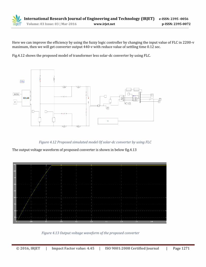
Here we can improve the efficiency by using the fuzzy logic controller by changing the input value of FLC in 2200-v maximum, then we will get converter output 440-v with reduce value of settling time 0.12 sec. Fig.4.12 shows the proposed model of transformer less solar-dc converter by using FLC.
Figure 4.12 Proposed simulated model Of solar-dc converter by using FLC
The output voltage waveform of proposed converter is shown in below fig.4.13
Figure 4.13 Output voltage waveform of the proposed converter
International Research Journal of Engineering and Technology (IRJET) e-ISSN: 2395 -0056
Volume: 03 Issue: 03 | Mar-2016 www.irjet.net p-ISSN: 2395-0072
© 2016, IRJET | Impact Factor value: 4.45 | ISO 9001:2008 Certified Journal | Page 1272
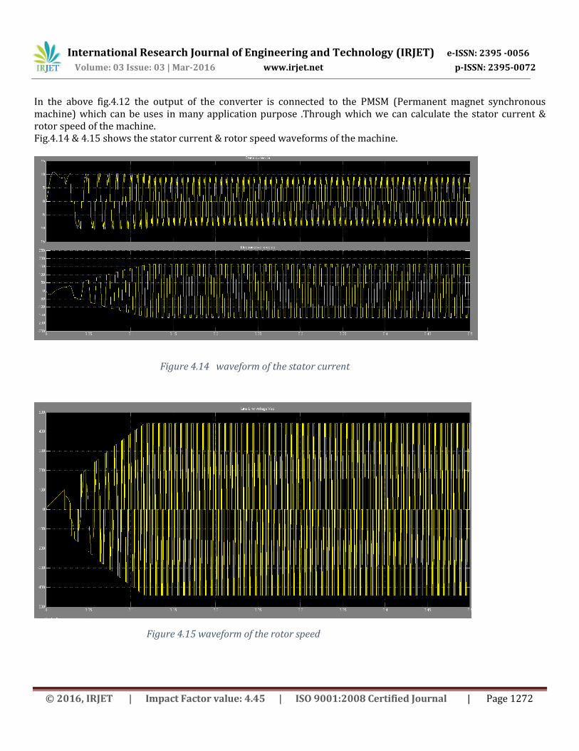
In the above fig.4.12 the output of the converter is connected to the PMSM (Permanent magnet synchronous machine) which can be uses in many application purpose .Through which we can calculate the stator current & rotor speed of the machine. Fig.4.14 & 4.15 shows the stator current & rotor speed waveforms of the machine.
Figure 4.14 waveform of the stator current
Figure 4.15 waveform of the rotor speed
International Research Journal of Engineering and Technology (IRJET) e-ISSN: 2395 -0056
Volume: 03 Issue: 03 | Mar-2016 www.irjet.net p-ISSN: 2395-0072
© 2016, IRJET | Impact Factor value: 4.45 | ISO 9001:2008 Certified Journal | Page 1273
CONCLUSION In this paper, a novel transformer-less adjustable voltage quadruple solar dc–dc converter with high voltage transfer gain with reduced value of settling time & semiconductor voltage stress by using FLC is proposed. The proposed topology utilizes input-parallel output-series configuration and is derived from a two-phase interleaved boost converter for providing a much higher voltage gain without adopting an extreme large duty cycle, This voltage can also be improve by using FLC which is connected at the output of the converter . This proposed converter cannot only achieve high step-up voltage gain but also reduce the settling time & voltage stress of both active switches and diodes. In addition, due to the charge balance of the blocking capacitor, the converter features automatic uniform current sharing characteristic of the two interleaved phases for voltage boosting mode without adding any extra circuitry or complex control methods. Finally this proposed converter provides 440-V output at 25-V input in 0.12 sec settling time. The proposed converter is very suitable for different applications requiring high step-up voltage gain.
REFERENCES 1.R. W. Erickson and D. Maksimovic, Fundamentals of Power Electronics, 2nd ed. Norwell, MA, USA: Kluwer, 2001. 2. Q. Zhao, F. Tao, F. C. Lee, P. Xu, and J.Wei, “A simple and effective to alleviate the rectifier reverse-recovery problem in continuous-current-mode boost converter,” IEEE Trans. Power Electron., vol. 16, no. 5, pp. 649–658, Sep. 2001. 3. Q. Zhao and Fred C. Lee, “High-Efficiency, High Step-Up DC–DC Converter,” IEEE Trans Power Electronic ,vol. 18, no. 1, jan. 2003.
4. N. P. Papanikolaou and E.C. Tatakis, “Active Voltage Clamp in Flyback Converters Operating in CCM Mode Under
Wide Load Variation,” IEEE Trans.on Ind. Electron. vol. 51, no. 3, june 2004.
5. Y. T. Jang and M. M. Jovanovic, “Interleaved boost converter with intrinsic voltage-doubler characteristic for universal-line PFC front end,” IEEE Trans. Power Electron., vol. 22, no. 4, pp. 1394–1401, Jul. 2007. 6. B.R. Lin, Senior Member, IEEE, and F.Y. Hsieh, “Soft-Switching Zeta–Flyback Converter With a Buck–Boost Type
of Active Clamp,” IEEE Trans.on Ind. Electron. vol. 54, no. 5, oct. 2007.
7. C. C. Ming Wang, “A Novel ZCS-PWM Flyback Converter With a Simple ZCS-PWM Commutation Cell,” IEEE
Trans.on Ind. Electron. vol. 55, no. 2, feb. 2008.
8. J. M. Kwon and B. H. Kwon, “High step-up active-clamp converter with input-current doubler and output-voltage doubler for fuel cell power systems,” IEEE Trans. Power Electron., vol. 24, no. 1, pp. 108–115, Jan. 2009. 9. L. S. Yang, T. J. Liang, and J. F. Chen, “Transformerless DC–DC converters with high step-up voltage gain,” IEEE Trans.on Ind. Electron., vol. 56, no. 8, pp. 3144–3152, Aug. 2009.
International Research Journal of Engineering and Technology (IRJET) e-ISSN: 2395 -0056
Volume: 03 Issue: 03 | Mar-2016 www.irjet.net p-ISSN: 2395-0072
© 2016, IRJET | Impact Factor value: 4.45 | ISO 9001:2008 Certified Journal | Page 1274
10. G. A. L. Henn, R. N. A. L. Silva, P. P. Praca, L. H. S. C. Barreto, and D. S. Oliveira, Jr., “Interleaved-boost converter with high voltage gain,” IEEE Trans. Power Electron., vol. 25, no. 11, pp. 2753–2761, Nov. 2010. 11. F.L.Tofoli ,D.D.C.Pereira, W.J.D. Paula, “survey on non isolated high-voltage step-up dc-dc topologies based on the boost converter,” IET Power Electronics, ISSN 1755-4535, 29th july 2014. 12. C.T.Pan, C.F. Chuang, and Chia-Chi Chu,“A Novel Transformer-less Adaptable Voltage Quadrupler DC Converter with Low Switch Voltage Stress,”IEEE Trans. Power electron., vol. 29, no. 9, Sep. 2014.