Embed Size (px)
Citation preview

Page 316
A Novel Realization and Synthesis of Ternary Content-Addressable
Memory (TCAM) Design Using Reversible Circuits
Vinjamuri C S Durga Prasad
M.Tech Student
Department of ECE
Sri Aditya Engineering College (JNTUK)
Surampalem, Andhra Pradesh - 533 437
M. Venkateswarlu, M.Tech
Sr. Assistant Professor
Department of ECE
Sri Aditya Engineering College (JNTUK)
Surampalem, Andhra Pradesh - 533 437
Abstract
Reversible computing is a model of computing where
the computational process to some extent is
reversible. A necessary condition for reversibility of a
computational model is that the relation of the
mapping states of transition functions to their
successors should at all times be one-to-one. Content
addressable memory is a special type of memory
which can do search operation in a single clock
cycle. CAM has disadvantages of high power
dissipation during the matching operation. Ternary
content addressable memory (TCAM) is a special type
of memory which is used to search for logic 0, logic
1, logic ’x’. These types of memory are used in
routers in order to perform the lookup table function
in a single clock cycle. As the use of networks,
typified by the Internet, has spread widely in recent
years, attention has focused on TCAMs as a key
device for increasing the speed of packet forwarding
(packet data transfers) by networking equipment by
enabling high-speed lookup of destinations, etc., for
large volumes of information during packet data
transfers. Reversible logic has gained its interest in
recent years due to its ultra low power characteristics.
Many works have been done to reduce the power
consumption in TCAM. This paper deals with a novel
design of TCAM cells using reversible logic. The
proposed design is optimized in terms of number of
garbage outputs and quantum cost. The proposed
TCAM cell does the function of the conventional
TCAM cell.
Keywords—TCAM, Garbage output, Quantum cost,
Reversible logic, Content addressable memory, Power
consumption
INTRODUCTION
Ternary content addressable memory compares input
data against stored data (logic ’0’, logic ’1’, don’t care)
in parallel and outputs the matched data. TCAM find
its applications in routers and some networking
equipment due to its deterministic and high speed
searches by using parallel operation to compare the
data stored with the search words. RAM needs an
address to fetch the data stored in the memory whereas
CAM needs the contents to be searched in the search
lines and the matched address is obtained at the output.
CAM is known for its high speed search operation.
However, the CAMs consume lot of power due to its
high speed operation and lot of heat is dissipated. High
power consumption in CAM devices increases the
junction temperatures of the chip which increases the
heat dissipation there by reducing the performance of
the chip. When there is computation in any logic
circuits, the loss in information will lead to heat
generation in the system. Landauer proposed that for
every single bit loss of information there will be KTln2
Joules of energy will be dissipated in the form of heat.
Bennett showed that heat dissipation will be zero
ideally if the circuit is designed using reversible
elements. According to the definition of reversible
elements, the circuit is said to be reversible if there is
no loss in information. Feynman has proposed the first
2×2 reversible gate which will do ex or operation.
Now-a-days, the research in designing the irreversible
circuits to reversible circuits is the great area of
concern due to its low power characteristics of the
design. In the conventional TCAM design, 16
transistors are used to do the search and match
operations. The change in state of the transistors due to
the changes in the bit of searchline and match-line will
Page 317
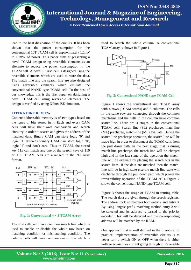
lead to the heat dissipation of the circuits. It has been
shown that the power consumption for the
conventional 16T TCAM cell is approximately 12mW
to 15mW of power. This paper aims at presenting a
novel TCAM design using reversible elements as an
alternate to reduce the power consumption in the
TCAM cell. A novel SRAM cell is designed using the
reversible elements which are used to store the data.
The match line and the search line are also designed
using reversible elements which emulate the
conventional NAND type TCAM cell. To the best of
our knowledge, this is the first paper on designing a
novel TCAM cell using reversible elements. The
design is verified by using Xilinx ISE simulator.
LITERATURE REVIEW
Content addressable memory is of two types based on
the types of bits stored in it. Each and every CAM
cells will have their own comparison and search
circuitry in order to search and gives the address of the
matched data. Binary CAM can store logic ’0’ and
logic ’1’ whereas ternary CAM can store logic ’0’,
logic ’1’ and don’t care. Thus in TCAM, the stored
key 11x can match any one of the search keys of 110
or 111. TCAM cells are arranged in the 2D array
format.
Fig. 1: Conventional 4 × 3 TCAM Array
The row cells will have common match line which is
used to enable or disable the whole row based on
matching condition or mismatching condition. The
column cells will have common search line which is
used to search the whole column. A conventional
TCAM array is shown in Figure 1.
Fig. 2: Conventional NAND type TCAM Cell
Figure 1 shows the conventional 4×3 TCAM array
with 4 rows (TCAM words) and 3 columns. The cells
in the same row are connected through the common
match-line and the cells in the column have common
search-line. There are 3 stages in the conventional
TCAM cell. Search line (SL) precharge, matchline
(ML) precharge, match-line (ML) evaluate. During the
search-line precharge operation, the search-line will be
made high in order to disconnect the TCAM cells from
the pull down path. In the next stage, that is during
match-line precharge, the match-line will be charged
high and in the last stage of the operation the match-
line will be evaluate by placing the search bits in the
search lines. If the data are matched then the match-
line will be in high state else the match line state will
discharge through the pull down path which proves the
irreversibility operation of the TCAM cells. Figure 2
shows the conventional NAND type TCAM cell.
Figure 3 shows the usage of TCAM in routing table.
The search data are given through the search registers.
The address look up matches both entry 2 and entry 3.
By using longest prefix matching method entry 2 will
be selected and its address is passed to the priority
encoder. This will be decoded and the corresponding
address will be matched by the RAM.
One approach that is well defined in the literature for
practical implementation of reversible circuits is to
never turn a switch ON or OFF when there is either
voltage across it or current going through it. Reversible

Page 318
energy recovery logic uses this approach in order to
avoid the non-adiabatic losses, which is essential for
an ultra low power energy system.
As a proof of concept for low power energy
consumption using reversible logic, an ultra low power
16-bit carry look ahead adder was proposed in using
reversible energy recovery logic.
Fig. 3: Application of TCAM in Routing Table
Fig. 4: Feynman Gate
REVERSIBLE ELEMENTS
This section discusses about the basics of reversible
elements. According to the definition of the reversible
circuit, there should not be any loss in the information.
The design constraints in the reversible circuit is that
the input and output vectors must map uniquely. There
should be equal number of inputs and outputs and fan
outs are not allowed in the design. Feedback from the
output to the input of the same gate is not allowed. The
design parameters in the reversible element design are
quantum cost, worst case delay and the garbage output.
Quantum cost is defined as the number of 1×1
reversible gate or 2 × 2 reversible gates. Worst case
delay is defined as the number of delay units to
produce the output for the given input. The worst case
delay of the 1×1 reversible gate is defined as 1 unit of
delay. Garbage output is the number of unused output
to ensure the reversibility property of the circuits
designed. Feynman has proposed the 2 × 2 Feynman
gate which performs the operation of the ex or gate.
Figure 4 shows the 2 × 2 Feynman gate with inputs
and outputs.
Figure 5 shows the 3 × 3 Fredkin gate with inputs and
outputs. As per the definition of quantum cost, the
quantum cost of 2 × 2 Feynman gate is 1 and 3 × 3
Fredkin gate is 5. Feynman gate can be used as the
fanout gate with one input as 0. Feynman gate can also
act as not gate with the B input as 1 which will invert
the value of A.
Fredkin gate can act as multiplexer with the input A as
the selection line. Peres has introduced 3 × 3 Peres
gate. Figure 6 shows the Peres gate. Peres gate can be
used as logical NAND or AND gate based on the
values of input C.
Fig. 5: Fredkin Gate
The quantum cost of the Peres gate is 4 and the worst
case delay is 4. Reversible element based SRAM cell
was designed in [9]. The main disadvantage in the
design [9] is that quantum cost of the proposed SRAM
cell can be further reduced and the reversible decoder
proposed does not contain enable signal which is
essential for chip select.

Page 319
Fig. 6: Peres Gate
SRAM CELL BASED ON REVERSIBLE
ELEMENTS
This section discusses about the novel SRAM cell
design based on reversible elements. Figure 7 shows
the proposed SRAM cell using reversible gates. In this
design, 3×3 Fredkin gate and the 2 × 2 Feynman gate
is used to form the SRAM cell which is used to store
the single bit of information. Each and every SRAM
cell will have word line (W L) in order to make the
SRAM cell to function in one of the modes that is
either in read/write or hold state. If the value of the W
L = 0 then the previous value has to be hold by the
SRAM cell. If the value of W L = 1, then the SRAM
will be in any one of the read/write state based on the
external write/sense circuits.
The WL output in the SRAM cell is used to enable the
row cells which emulate the functionality of the
conventional SRAM cell. Quantum cost for the
proposed SRAM cell is 6. Figure 8 shows the SRAM
cell with read/write enable with the row decoder. The
quantum cost of this design is 16 which is still less as
compared to the SRAM cell proposed in [9]. This
design is used to store the bit in the TCAM memory
cells.
The design proposed in Figure 8 emulates the
functionality of SRAM array with the reversible read
circuits, reversible write circuits. The row decoder in
[10] is used in the designing of SRAM array.
The quantum cost of the decoder proposed in [9] is 10
whereas the quantum cost of the decoder proposed in
[10] is 15. But the decoder proposed in [10] is with the
enable bit which is very essential in the design of
memories for the chip select.
Fig. 7: SRAM Cell using Reversible Gates
PROPOSED TCAM CELL USING REVERSIBLE
ELEMENTS
This section discusses about the proposed TCAM cell
using reversible elements. Figure 9 shows the
proposed TCAM cell. SRAM cell discussed in the
previous section is used to store the bits. The data will
be stored initially in the SRAM cell using the
reversible SRAM cell as discussed in the previous
section. The data stored will be passed to the 2 × 2
Feynman gate with the search line as one input. So, the
search line will be duplicated and ex-or operation of
data and the search-line data will be the other output. If
both search line data and the data stored are same, then
the output of the Feynman gate is search-line data and
zero. The search line data will be passed to the next
TCAM cell of the same column. The output of ex-or
operated value is passed to the next 2 × 2 Feynman
gate which will act like a not gate with one of the input
as constant input 1. So, if the ex-or operated value is 0,
then the output of second Feynman is logic ’1’. The
value obtained in the second 2 × 2 Feynman gate is
passed to the 3 × 3 Fredkin gate. Inputs to the 3 × 3
Fredkin gate are match bit (M), output from 2 × 2
Feynman gate and the constant value of logic ’1’.
Table I illustrates the functionality of the TCAM cell
using the match bit.
Page 320
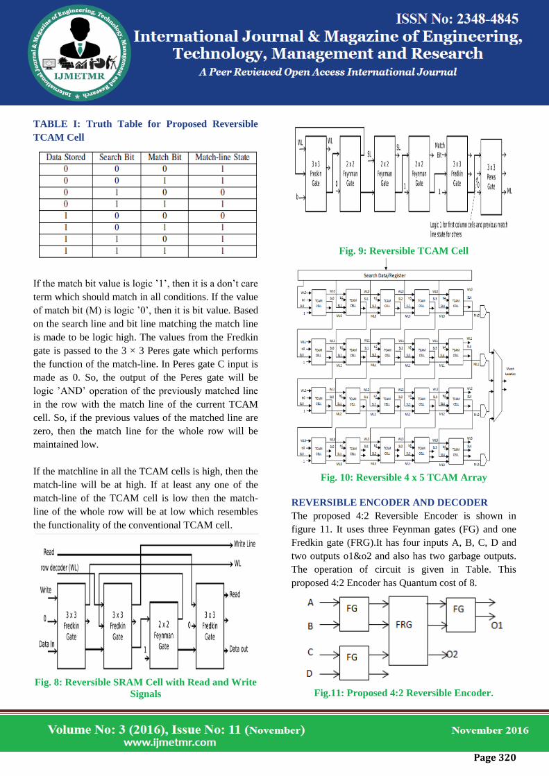
TABLE I: Truth Table for Proposed Reversible
TCAM Cell
If the match bit value is logic ’1’, then it is a don’t care
term which should match in all conditions. If the value
of match bit (M) is logic ’0’, then it is bit value. Based
on the search line and bit line matching the match line
is made to be logic high. The values from the Fredkin
gate is passed to the 3 × 3 Peres gate which performs
the function of the match-line. In Peres gate C input is
made as 0. So, the output of the Peres gate will be
logic ’AND’ operation of the previously matched line
in the row with the match line of the current TCAM
cell. So, if the previous values of the matched line are
zero, then the match line for the whole row will be
maintained low.
If the matchline in all the TCAM cells is high, then the
match-line will be at high. If at least any one of the
match-line of the TCAM cell is low then the match-
line of the whole row will be at low which resembles
the functionality of the conventional TCAM cell.
Fig. 8: Reversible SRAM Cell with Read and Write
Signals
Fig. 9: Reversible TCAM Cell
Fig. 10: Reversible 4 x 5 TCAM Array
REVERSIBLE ENCODER AND DECODER
The proposed 4:2 Reversible Encoder is shown in
figure 11. It uses three Feynman gates (FG) and one
Fredkin gate (FRG).It has four inputs A, B, C, D and
two outputs o1&o2 and also has two garbage outputs.
The operation of circuit is given in Table. This
proposed 4:2 Encoder has Quantum cost of 8.
Fig.11: Proposed 4:2 Reversible Encoder.

Page 321
A single Fredkin gate is capable of working like a 1:2
decoder if the first input is IN1, while the second and
third inputs are 0 and 1 respectively. A design of 2:4
decoder using 3 Fredkin gates has been proposed, as
shown in Figure 12. The quantum cost of this design is
15.
Fig: 12: Proposed reversible 2:4 decoder
SEARCH OPERATION IN TCAM ARRAY
This section discusses about the operation of TCAM
array and how the data are searched and matched.
Figure.10 proposes the 4 × 5 reversible TCAM array.
The data are stored in each TCAM cell using normal
SRAM operation. Once the data is stored in the TCAM
cell, match bit will be set either logic ’0’ or logic ’1’
based on whether the stored value is bit or don’t care.
Search data are passed to the corresponding TCAM
cell from search data registers.
Let us assume the data stored in the first row of the
TCAM array be0011X and the data in the search-line
be00101. SL1 data that is 1 is ex-ored with data value
that is 1. So the output of the ex-or operation is 0.
Whenever the data are matched the output of the ex-or
operation is 0 which is then inverted to get the output
1. This resembles the functionality of the conventional
binary CAM cell. The data stored in the TCAM is
either logic ’0’/logic ’1’ or don’t care bit based on the
value of the match bit.
TABL II: Design metrics of Reversible Ternary
Contents Address Memory inters of Garbage
Outputs (GO), Quantum Cost (QC), Gate Count
(GC) and Constant Inputs (CI).
If the value of the match bit is ’0’ then the data will be
either logic ’0’ or logic ’1’. If the match bit is ’1’ then
the data stored is don’t care. If M = 1, then the output
is logic ’1’ at all cases of input. If the value of M = 0
then the output will be logic ’0’ or logic ’1’ based on
the matching of search data and the data stored. The
output from the 3 × 3 Fredkin gate is passed to the 3 ×
3 Peres gate.
The inputs to the Peres gate are the output from the 3 ×
3 Fredkin gate, previous matchline values and the
constant input ’0’. The previous match-line value of
the first TCAM cell is set to be 1 which resembles the
match line precharge in the conventional TCAM cell.
The match-line output of the first TCAM cell is passed
to the 3×3 Peres gate of the second TCAM cell.
If the match-line of the first TCAM cell is zero then
the whole match-line has to be pull down to zero. So,
the match-line which is zero is ’and’ operated with the
second match-line which will result in the match line
low. This shows the operation of reversible TCAM
array which performs the same operation of the
conventional TCAM array. The match-line is passed
through the whole row of the cell and the search line is
passed to the whole column of the TCAM cell.
SIMULATION RESULTS
All the synthesis and simulation results are performed
using Verilog HDL. The synthesis and simulation are
performed on Xilinx ISE 14.4. The simulation results
are shown below figures.

Page 322
Fig. 13: RTL schematic of Reversible 4X5 TCAM
Array
Fig. 14: RTL sub schematic of Reversible 4X5
TCAM Array
Fig. 15: Technology schematic of Reversible 4X5
TCAM Array
Fig. 16: Design summary of Reversible 4X5 TCAM
Array
Fig. 17: Simulation of Reversible 4X5 TCAM Array
Page 323
CONCLUSION AND FUTURE WORK
This paper proposed a novel design of 4x5 TCAM
array design using reversible circuit design. Ternary
content addressable memory compares input data
against stored data (logic ’0’, logic ’1’, don’t care) in
parallel and outputs the matched data. In reversible
SRAM design, 3 × 3 Fredkin gate and the 2 × 2
Feynman gate is used to form the SRAM cell which is
used to store the single bit of information. Each and
every SRAM cell will have word line (WL) in order to
make the SRAM cell to function in one of the modes
that is either in read/write or hold state. 3×3 Fredkin
gate and Peres gate are used to perform the search line
and match line operation. The design is verified and
simulated by using Xilinx ISE simulator. The practical
realization of reversible TCAM based chip will
definitely reduce the power consumption of the
network switches. In future the proposed Ternary
Content Address Memory (TCAM) can be used in
networking and routers applications for high speed
data searching.
REFERENCES
[1] N. Mohan, W. Fung, D. Wright, and M. Sachdev,
“Design techniques and test methodology for low-
power tcams,” Very Large Scale Integration (VLSI)
Systems, IEEE Transactions on, vol. 14, no. 6, pp.
573–586, 2006.
[2] R. Landauer, “Irreversibility and heat generation in
the computing process,” IBM Journal of Research and
Development, vol. 5, no. 3, pp. 183–191, July 1961.
[3] C. Bennett, “Logical reversibility of computation,”
IBM Journal of Research and Development, vol. 17,
no. 6, pp. 525–532, Nov 1973.
[4] R. Feynman, “Quantum mechanical computers,”
Foundations of Physics, vol. 16, no. 6, pp. 507–531,
1986.
[5] F. Zane, G. Narlikar, and A. Basu, “Coolcams:
Power-efficient tcams for forwarding engines,” in
INFOCOM 2003. Twenty-Second Annual Joint
Conference of the IEEE Computer and
Communications. IEEE Societies, vol. 1. IEEE, 2003,
pp. 42–52.
[6] K. Pagiamtzis and A. Sheikholeslami, “Content-
addressable memory (cam) circuits and architectures: a
tutorial and survey,” Solid-State Circuits, IEEE
Journal of, vol. 41, no. 3, pp. 712–727, March 2006.
[7] J. Lim, D.-G.Kim, and S.-I.Chae, “A 16-bit carry-
lookahead adder using reversible energy recovery
logic for ultra-low-energy systems,” Solid-State
Circuits, IEEE Journal of, vol. 34, no. 6, pp. 898–903,
1999.
[8] A. Peres, “Reversible logic and quantum
computers,” Physical review A, vol. 32, no. 6, p. 3266,
1985.
[9] M. Morrison, M. Lewandowski, R. Meana, and N.
Ranganathan, “Design of static and dynamic ram
arrays using a novel reversible logic gate and
decoder,” in Nanotechnology (IEEE-NANO), 2011
11th IEEE Conference on, Aug 2011, pp. 417–420.
[10] S. Mahammad and K. Veezhinathan,
“Constructing online testable circuits using reversible
logic,” Instrumentation and Measurement, IEEE
Transactions on, vol. 59, no. 1, pp. 101–109, Jan 2010.