Embed Size (px)
Citation preview
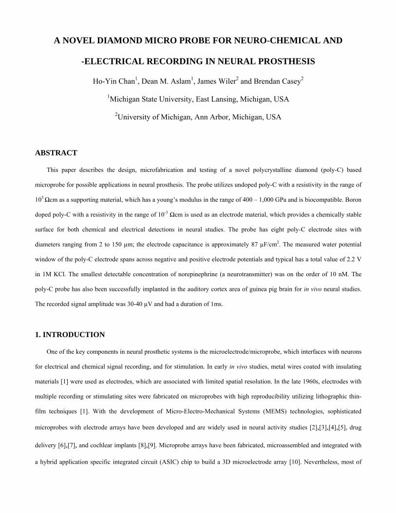
A NOVEL DIAMOND MICRO PROBE FOR NEURO-CHEMICAL AND
-ELECTRICAL RECORDING IN NEURAL PROSTHESIS
Ho-Yin Chan1, Dean M. Aslam1, James Wiler2 and Brendan Casey2
1Michigan State University, East Lansing, Michigan, USA
2University of Michigan, Ann Arbor, Michigan, USA
ABSTRACT
This paper describes the design, microfabrication and testing of a novel polycrystalline diamond (poly-C) based
microprobe for possible applications in neural prosthesis. The probe utilizes undoped poly-C with a resistivity in the range of
105 Ωcm as a supporting material, which has a young’s modulus in the range of 400 – 1,000 GPa and is biocompatible. Boron
doped poly-C with a resistivity in the range of 10-3 Ωcm is used as an electrode material, which provides a chemically stable
surface for both chemical and electrical detections in neural studies. The probe has eight poly-C electrode sites with
diameters ranging from 2 to 150 µm; the electrode capacitance is approximately 87 µF/cm2. The measured water potential
window of the poly-C electrode spans across negative and positive electrode potentials and typical has a total value of 2.2 V
in 1M KCl. The smallest detectable concentration of norepinephrine (a neurotransmitter) was on the order of 10 nM. The
poly-C probe has also been successfully implanted in the auditory cortex area of guinea pig brain for in vivo neural studies.
The recorded signal amplitude was 30-40 µV and had a duration of 1ms.
1. INTRODUCTION
One of the key components in neural prosthetic systems is the microelectrode/microprobe, which interfaces with neurons
for electrical and chemical signal recording, and for stimulation. In early in vivo studies, metal wires coated with insulating
materials [1] were used as electrodes, which are associated with limited spatial resolution. In the late 1960s, electrodes with
multiple recording or stimulating sites were fabricated on microprobes with high reproducibility utilizing lithographic thin-
film techniques [1]. With the development of Micro-Electro-Mechanical Systems (MEMS) technologies, sophisticated
microprobes with electrode arrays have been developed and are widely used in neural activity studies [2],[3],[4],[5], drug
delivery [6],[7], and cochlear implants [8],[9]. Microprobe arrays have been fabricated, microassembled and integrated with
a hybrid application specific integrated circuit (ASIC) chip to build a 3D microelectrode array [10]. Nevertheless, most of
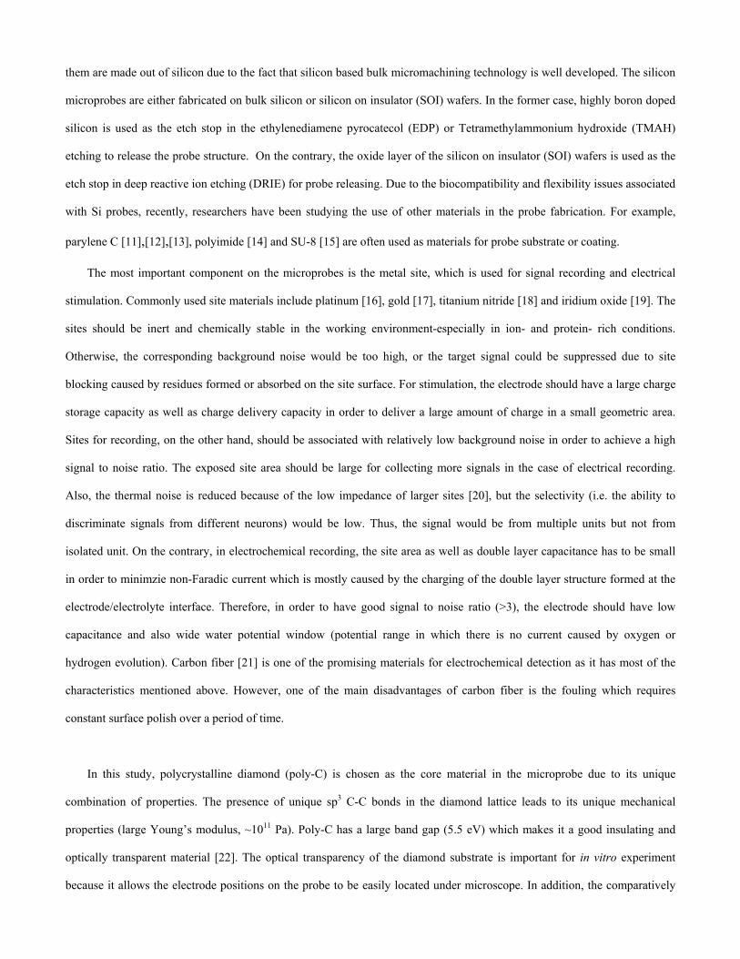
them are made out of silicon due to the fact that silicon based bulk micromachining technology is well developed. The silicon
microprobes are either fabricated on bulk silicon or silicon on insulator (SOI) wafers. In the former case, highly boron doped
silicon is used as the etch stop in the ethylenediamene pyrocatecol (EDP) or Tetramethylammonium hydroxide (TMAH)
etching to release the probe structure. On the contrary, the oxide layer of the silicon on insulator (SOI) wafers is used as the
etch stop in deep reactive ion etching (DRIE) for probe releasing. Due to the biocompatibility and flexibility issues associated
with Si probes, recently, researchers have been studying the use of other materials in the probe fabrication. For example,
parylene C [11],[12],[13], polyimide [14] and SU-8 [15] are often used as materials for probe substrate or coating.
The most important component on the microprobes is the metal site, which is used for signal recording and electrical
stimulation. Commonly used site materials include platinum [16], gold [17], titanium nitride [18] and iridium oxide [19]. The
sites should be inert and chemically stable in the working environment-especially in ion- and protein- rich conditions.
Otherwise, the corresponding background noise would be too high, or the target signal could be suppressed due to site
blocking caused by residues formed or absorbed on the site surface. For stimulation, the electrode should have a large charge
storage capacity as well as charge delivery capacity in order to deliver a large amount of charge in a small geometric area.
Sites for recording, on the other hand, should be associated with relatively low background noise in order to achieve a high
signal to noise ratio. The exposed site area should be large for collecting more signals in the case of electrical recording.
Also, the thermal noise is reduced because of the low impedance of larger sites [20], but the selectivity (i.e. the ability to
discriminate signals from different neurons) would be low. Thus, the signal would be from multiple units but not from
isolated unit. On the contrary, in electrochemical recording, the site area as well as double layer capacitance has to be small
in order to minimzie non-Faradic current which is mostly caused by the charging of the double layer structure formed at the
electrode/electrolyte interface. Therefore, in order to have good signal to noise ratio (>3), the electrode should have low
capacitance and also wide water potential window (potential range in which there is no current caused by oxygen or
hydrogen evolution). Carbon fiber [21] is one of the promising materials for electrochemical detection as it has most of the
characteristics mentioned above. However, one of the main disadvantages of carbon fiber is the fouling which requires
constant surface polish over a period of time.
In this study, polycrystalline diamond (poly-C) is chosen as the core material in the microprobe due to its unique
combination of properties. The presence of unique sp3 C-C bonds in the diamond lattice leads to its unique mechanical
properties (large Young’s modulus, ~1011 Pa). Poly-C has a large band gap (5.5 eV) which makes it a good insulating and
optically transparent material [22]. The optical transparency of the diamond substrate is important for in vitro experiment
because it allows the electrode positions on the probe to be easily located under microscope. In addition, the comparatively
wide total potential window (the reported values range from 1.4 to 4 V) in an aqueous environment [23],[24],[25],[26], low
double layer capacitance (ranging from 5 to 40 µF/cm2) [27], chemical inertness and stability, resistance to fouling of boron-
doped diamond make it an excellent site material for microprobes [23]. The biocompatibility of diamond surfaces has been
studied intensively based on the protein adsorption and cellular responses on chemical-vapor-deposited (CVD) diamond [28]
and diamond-liked carbon (DLC) [29]. It is found that CVD diamond absorbed and denatured relatively small amounts of
fibrinogen which is commonly used as a biocompatibility indicator, and there is no cytotoxicity, inflammatory reaction and
adverse effects on cells [30]. In electrochemistry, researchers have extensively studied boron-doped diamond as an electrode
material [31],[32]. The boron doped poly-C electrodes, used in neural studies [33],[34], were fabricated by depositing
diamond on the tip of a wire. These electrodes display limited spatial resolution for studying brain activities. Recently, poly-
C sensors and electrodes were integrated in Si cochlear microprobes for the first time [9].
In this paper, diamond based neural probes (poly-C neural probes) are designed, fabricated and tested for the first time.
The poly-C neural probes, each having a precisely positioned array of electrodes with micrometer or nanometer dimensions,
make it possible to detect multiple chemical and electrical signals with a single probe structure. A unique feature of such
probes is that they use undoped poly-C as a mechanical material and boron-doped poly-C as a site/lead material, making it
possible to fabricate all-diamond probes.
2. DIAMOND MICROMACHINING TECHNOLOGIES
Important processes in the micromachining of poly-C include diamond seeding, diamond growth and doping, and
diamond dry-etching. While the first two processes have been investigated extensively in past studies [35], the optimization
of dry etching of diamond has been accomplished for neural probe fabrication for the first time in the current study.
A. Diamond Seeding
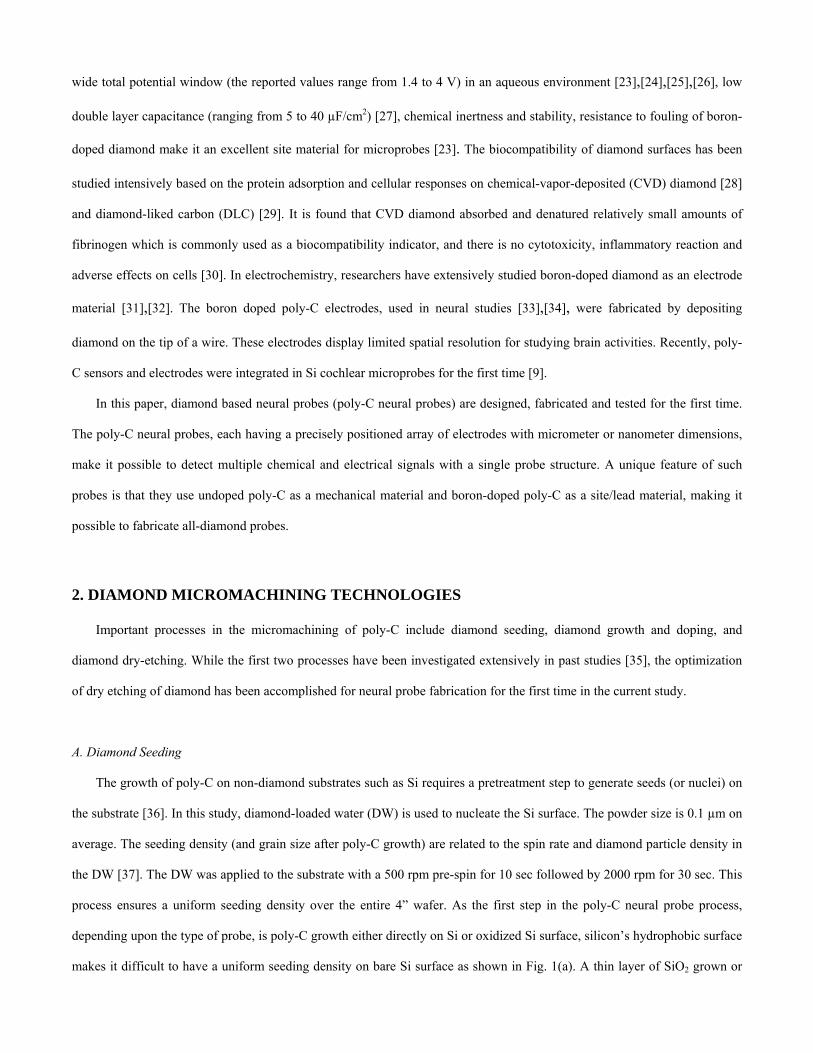
The growth of poly-C on non-diamond substrates such as Si requires a pretreatment step to generate seeds (or nuclei) on
the substrate [36]. In this study, diamond-loaded water (DW) is used to nucleate the Si surface. The powder size is 0.1 µm on
average. The seeding density (and grain size after poly-C growth) are related to the spin rate and diamond particle density in
the DW [37]. The DW was applied to the substrate with a 500 rpm pre-spin for 10 sec followed by 2000 rpm for 30 sec. This
process ensures a uniform seeding density over the entire 4” wafer. As the first step in the poly-C neural probe process,
depending upon the type of probe, is poly-C growth either directly on Si or oxidized Si surface, silicon’s hydrophobic surface
makes it difficult to have a uniform seeding density on bare Si surface as shown in Fig. 1(a). A thin layer of SiO2 grown or
d
H
c
F
s
B
T
h
p
a
R
u
d
f
F
w
deposited on S
HCL:H2O:H2O
cleaning of Si
Fig. 1(b). The r
surface the unif
B. Diamond Gr
Microwave
TABLE I [37].
hydrogen. The
phase); the res
approximately
Raman peak sh
As poly
until it is fully
different types
film, tc, is impo
Fig. 3. The resu
which leads an
Si can solve
O2) chemically
surface throug
resulting seedi
formity of DW
Fig. 1.
rowth and Dop
e Plasma Chem
. The diamond
boron doping
sistivity is in
2 µm. The fil
hown in Fig. 2.
y-C is grown a
covered by po
of commonly
ortant if SiO2 i
ulting seeding
increase in tc.
this problem.
oxidizes the S
gh first half of
ing density is i
W is not a proble
. Seed distribut
ping
mical Vapor D
d film was in-s
level, accordin
the range of
lm quality, as
at 750oC, hydro
oly-C. This can
used SiO2 lay
is used as an in
density is also
It has been
Si surface, whi
f the RCA clea
in the range of
em.
(a)
tion on (a) a no
Deposition (MP
itu boron dope
ng to data pres
10-1 - 10-3 Ωc
indicated by t
ogen plasma co
n cause problem
yers are listed
nsulator. This
o plotted. It is n
reported [38]
ch makes it hy
aning process i
f 109 – 1010 cm
on-treated and
PCVD) was us
ed by introduc
sented in [37],
cm. The avera
the sp3/sp2 C-C
ontinues to etc
ms if the SiO2
in TABLE II.
time, tc, is plo
noted that as th
that the first
ydrophilic. Thu
improves the u
m-2. If the fabri
(b)
(b) an RCA-tre
ed for the poly
cing trimethylb
is in the range
age grain size
C bond ratio, i
ch SiO2 through
2 layer is used
A knowledge
otted as a funct
he spin speed i
t half of RCA
us, prior to the
uniformity of D
ication process
eated Si surfac
y-C growth us
boron (TMB), (
e of 3000 - 700
on the surfac
is very good a
h the holes bet
as an insulatin
of time requir
tion of spin sp
increases, the s
A-clean (NH3:H
e application o
DW seeding as
s starts on an o
ce.
ing parameters
(B(CH3)3), gas
00 ppm (B/C r
ce of the poly
as indicated by
tween the diam
ng layer. The e
red to form a c
peed for DW as
seeding density
H2O:H2O2,
of DW, the
s shown in
oxidized Si
s shown in
s diluted in
ratio in gas
y-C film is
y the sharp
mond seeds
etch rate of
continuous
s shown in
y decreases
Fig.
SMethTherLPCPEC
Cond
Parameter(
Growth Temp
Growth PressGases Used f
Dopant Used Poly-C Microwave PGrowth Growth Rate
Poly-C Film TUndoped/Dop
(a)
. 2. (a) An SEM
Etch rat
SiO2 Growth/hod Temrmal VD VD
ditions for Diam
(s)
perature
sure for Growth
for B-doped
Power Used for
Thickness; ped
M image of a p
T
tes of un-annea
/Deposition mperature (oC
1100 450 380
TABLE I
mond Growth U
Value(s)
750 oC
40 Torr Methane: 1 sHydrogen: 10
Trimethylbor(0.1% of BH2): 5-10 scc2.3 kW, 2.4 G
0.10 - 0.15 µ
3 µm/ 0.5 µm
oly-C surface a
TABLE II
aled SiO2 durin
SiO2 EtchGrowthC)
Using MPCVD
sccm 00 sccm
ron diluted in HB(CH3)3 by vocm GHz
µm/h
m
(
and (b) its Ram
ng poly-C grow
h Rate (nm/mh Temperatur
1.0 - 3.01.4 - 3.12.8 - 4.4
D
H2 olume in
b)
man spectrum.
wth.
min) at Poly-C re of 750 oC
C
n
s
p
f
i
s
tw
p
T
F
C. Diamond Dr
Although t
neural probe fa
stages of dry et
poly-C film, ho
fluorine, the un
s well known
sputtering of A
wo step etchin
presence of onl
This process le
ig. 3. The relat
ry Etching
the reactive ion
abrication in th
tching of poly
oles appear in t
nderlying subst
that micro co
Al by O2 plasma
ng process was
ly CF4 until a v
ads to smooth
tionships betwe
n etching of dia
he current wo
y-C are shown
the poly-C film
trate (Si or SiO
olumns (due t
a. The showeri
s developed to
very thin poly-
Si or SiO2 surf
een the seeding
amond has bee
rk (see TABL
in Fig. 4. As t
m as seen in Fig
O2) is etched wh
o micromaskin
ing of sputtered
eliminate micr
-C film is left o
face with a rou
g density and t
en studied inten
LE III) has bee
the etching of
g. 4(c). At this
hich increases
ng) would be
d Al particles o
romasking and
on the surface.
ughness of appr
time tc as a fun
nsively [39],[4
en problematic
poly-C contin
s stage of etchi
its roughness.
formed in the
on the surface
d substrate etch
Then, the fina
roximately 3 n
ction of seedin
0],[41], poly-
c. SEM microg
nues to reach th
ng process, if t
However, in t
e etching gase
being etched l
hing [43]. First
al etching stage
nm.
ng spin rate.
C dry etching u
graphs taken a
he seeding por
the etching gas
the absence of
es [42], which
eads to microm
t, poly-C is etc
e is done in pu
used in the
at different
rtion of the
ses contain
fluorine, it
h is due to
masking. A
ched in the
ure oxygen.
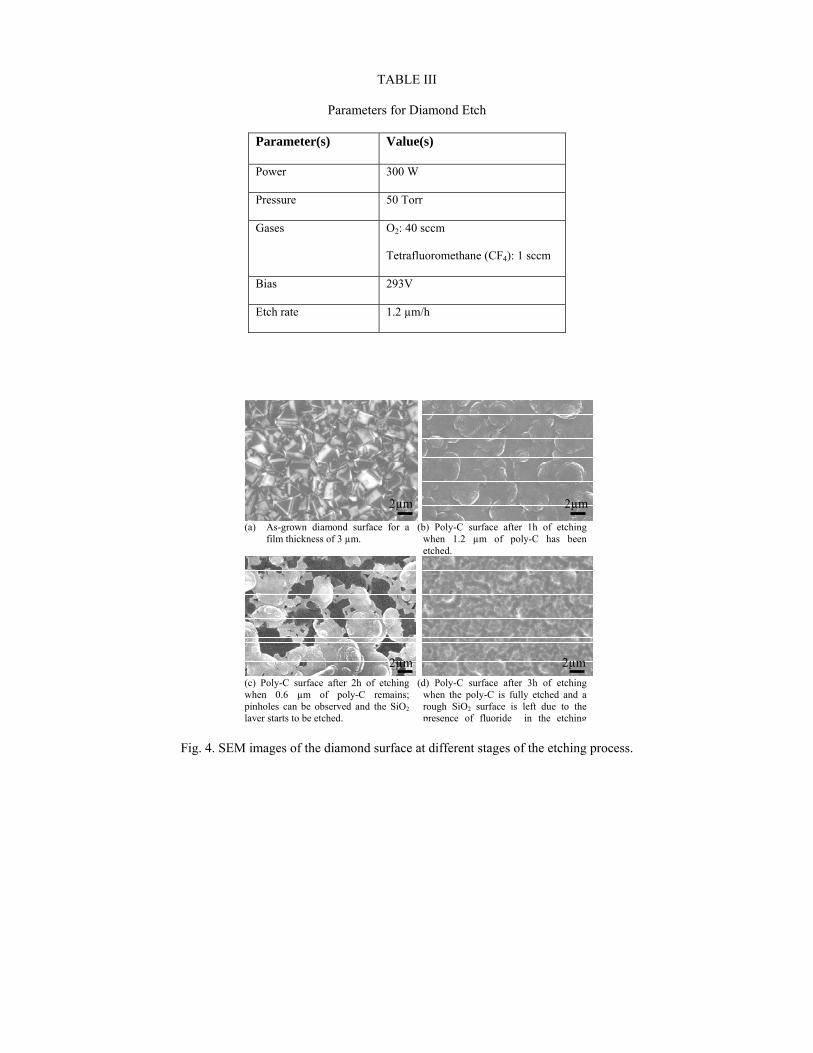
TABLE III
Parameters for Diamond Etch
Parameter(s) Value(s)
Power 300 W
Pressure 50 Torr
Gases O2: 40 sccm
Tetrafluoromethane (CF4): 1 sccm
Bias 293V
Etch rate 1.2 µm/h
(a) As-grown diamond surface for a film thickness of 3 µm.
(b) Poly-C surface after 1h of etching when 1.2 µm of poly-C has been etched.
(c) Poly-C surface after 2h of etching when 0.6 µm of poly-C remains; pinholes can be observed and the SiO2 layer starts to be etched.
(d) Poly-C surface after 3h of etching when the poly-C is fully etched and a rough SiO2 surface is left due to the presence of fluoride in the etching
2µm 2µm
2µm 2µm
Fig. 4. SEM images of the diamond surface at different stages of the etching process.
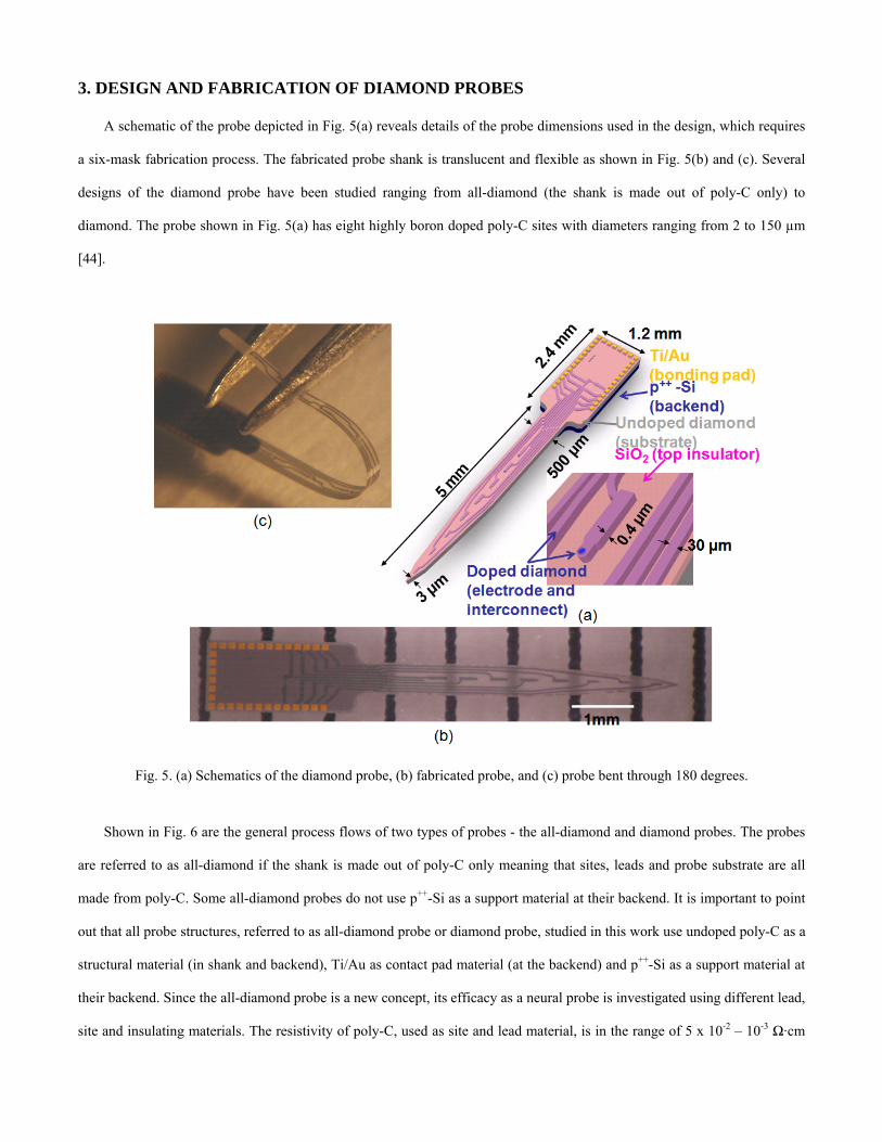
3. DESIGN AND FABRICATION OF DIAMOND PROBES
A schematic of the probe depicted in Fig. 5(a) reveals details of the probe dimensions used in the design, which requires
a six-mask fabrication process. The fabricated probe shank is translucent and flexible as shown in Fig. 5(b) and (c). Several
designs of the diamond probe have been studied ranging from all-diamond (the shank is made out of poly-C only) to
diamond. The probe shown in Fig. 5(a) has eight highly boron doped poly-C sites with diameters ranging from 2 to 150 µm
[44].
Fig. 5. (a) Schematics of the diamond probe, (b) fabricated probe, and (c) probe bent through 180 degrees.
Shown in Fig. 6 are the general process flows of two types of probes - the all-diamond and diamond probes. The probes
are referred to as all-diamond if the shank is made out of poly-C only meaning that sites, leads and probe substrate are all
made from poly-C. Some all-diamond probes do not use p++-Si as a support material at their backend. It is important to point
out that all probe structures, referred to as all-diamond probe or diamond probe, studied in this work use undoped poly-C as a
structural material (in shank and backend), Ti/Au as contact pad material (at the backend) and p++-Si as a support material at
their backend. Since the all-diamond probe is a new concept, its efficacy as a neural probe is investigated using different lead,
site and insulating materials. The resistivity of poly-C, used as site and lead material, is in the range of 5 x 10⁻² – 10-3 Ω·cm
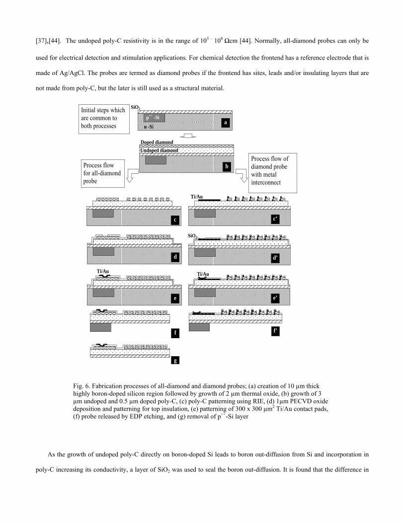
[37],[44]. The undoped poly-C resistivity is in the range of 105 – 108 Ωcm [44]. Normally, all-diamond probes can only be
used for electrical detection and stimulation applications. For chemical detection the frontend has a reference electrode that is
made of Ag/AgCl. The probes are termed as diamond probes if the frontend has sites, leads and/or insulating layers that are
not made from poly-C, but the later is still used as a structural material.
Fig. 6. Fabrication processes of all-diamond and diamond probes; (a) creation of 10 µm thick highly boron-doped silicon region followed by growth of 2 µm thermal oxide, (b) growth of 3 µm undoped and 0.5 µm doped poly-C, (c) poly-C patterning using RIE, (d) 1µm PECVD oxide deposition and patterning for top insulation, (e) patterning of 300 x 300 µm2 Ti/Au contact pads, (f) probe released by EDP etching, and (g) removal of p++-Si layer
As the growth of undoped poly-C directly on boron-doped Si leads to boron out-diffusion from Si and incorporation in
poly-C increasing its conductivity, a layer of SiO2 was used to seal the boron out-diffusion. It is found that the difference in
a
b
c
f
d
e
d’
c’
e’
f’
p++ -Si
n -Si
SiO2
Undoped diamond Doped diamond
Ti/Au
SiO2
Ti/Au Ti/Au
Initial steps which are common to both processes
Process flow for all-diamond probe
Process flow of diamond probe with metal interconnect
g
the resistivities of diamond films on Si substrate with and without SiO2 protection can be 2 orders in magnitude. Therefore,
SiO2 is an essential layer for diamond growth on a boron doped silicon substrate (Fig. 6(a)). A 1.5 µm thick thermal oxide is
needed to suppress the boron out-diffusion by taking into account the fact that SiO2 can be etched during the initial phase of
poly-C growth when the poly-C film is not continuous. Aluminum (700 nm) was used as the mask for dry etching (Fig. 6(c)).
The etching of the undoped/highly doped diamond stack was monitored by measuring the resistivity of the etched surface and
the step height of the patterns. As the resistivity exceeds 105 Ωcm, the doped poly-C has been fully etched. The undoped
poly-C serves as the substrate for the probe, while the highly doped poly-C is for the sites and leads. In the case of using
metals as the lead material, an additional step is added to pattern a Ti/Au (50nm/300nm) layer (Fig. 6(c’)). Then, a 1.4 µm
PECVD SiO2 layer was deposited. This layer was patterned and etched using a buffered oxide solution in order to expose the
contact pads (located on the backend) and the diamond sites (Fig. 6(d) & (d’)). A layer of titanium/gold (50 nm/300 nm) was
then deposited and patterned to form the contact pads (Fig. 6(e) & (e’)). Finally, the Si substrate was thinned by HF-nitric
(HNA) down to 200 µm and the probes were released using the ethylene-diamine-pyrocatechol (EDP) process (Fig. 6(f) &
(f’)) with boron etch stop. For some probes the p++-Si layer was removed (Fig. 6(g)).
4. EXPERIMENTAL RESULTS AND DISCUSSIONS
The testing of poly-C neural probes consisted of electrode modeling, electrode comparison, chemical detection and
in vivo electrical detection. A potentiostat (model # CH750C by CH Instruments) with a three electrode configuration
(working, counter and reference electrodes) was used for electrochemical measurements and a Faraday cage was used for
minimizing the surrounding noise. Electrical Impedance Spectroscopy (EIS) was used for electrode modeling and
characterizing the electrode behavior in a wide range of frequencies [45],[46]. Cyclic Voltammograms (CV) were used for
studying the electrode reactions, which give information not only on the thermodynamics at reactions but also on kinetic
parameters (e.g. heterogeneous electron-transfer rate constant). The working, counter and reference electrodes were
diamond, platinum and Ag/AgCl, respectively. The potential sweep rate is 100 mV/s.
The in vivo electrical detection was done in the Kresge Hearing Research Institute at the University of Michigan and
performed on pigmented guinea pigs using approved animal use and care procedures. The poly-C probe was placed in the
auditory cortex in the right hemisphere of the guinea pig’s brain, which was connected to a Plexon Neural Data Acquisition
System to record the stimulated neural signals.
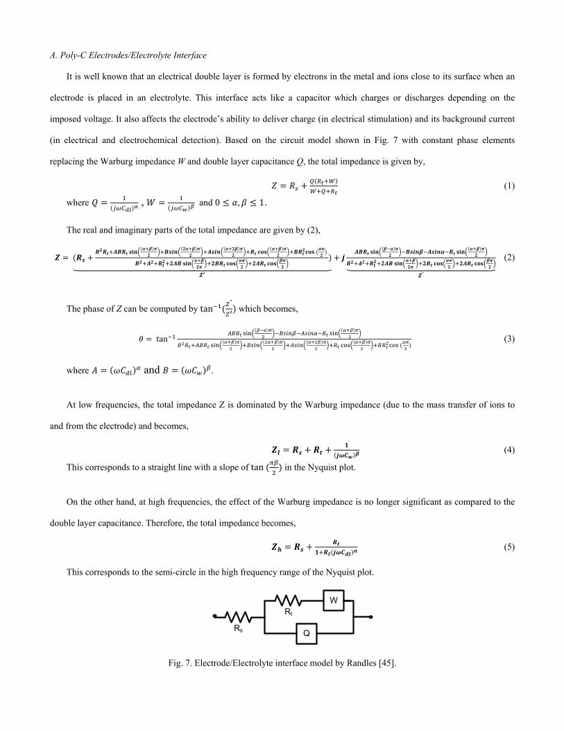
A. Poly-C Electrodes/Electrolyte Interface
It is well known that an electrical double layer is formed by electrons in the metal and ions close to its surface when an
electrode is placed in an electrolyte. This interface acts like a capacitor which charges or discharges depending on the
imposed voltage. It also affects the electrode’s ability to deliver charge (in electrical stimulation) and its background current
(in electrical and electrochemical detection). Based on the circuit model shown in Fig. 7 with constant phase elements
replacing the Warburg impedance W and double layer capacitance Q, the total impedance is given by,
(1) where , and 0 , 1.
The real and imaginary parts of the total impedance are given by (2),
"
(2)
The phase of Z can be computed by tan"
which becomes,
tan
(3)
where and .
At low frequencies, the total impedance Z is dominated by the Warburg impedance (due to the mass transfer of ions to
and from the electrode) and becomes,
(4)
This corresponds to a straight line with a slope of tan in the Nyquist plot.
On the other hand, at high frequencies, the effect of the Warburg impedance is no longer significant as compared to the
double layer capacitance. Therefore, the total impedance becomes,
(5)
This corresponds to the semi-circle in the high frequency range of the Nyquist plot.
Rs
Rt
W
Q
Fig. 7. Electrode/Electrolyte interface model by Randles [45].
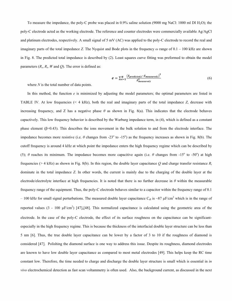
To measure the impedance, the poly-C probe was placed in 0.9% saline solution (9000 mg NaCl: 1000 ml DI H2O); the
poly-C electrode acted as the working electrode. The reference and counter electrodes were commercially available Ag/AgCl
and platinum electrodes, respectively. A small signal of 5 mV (AC) was applied to the poly-C electrode to record the real and
imaginary parts of the total impedance Z. The Nyquist and Bode plots in the frequency ω range of 0.1 – 100 kHz are shown
in Fig. 8. The predicted total impedance is described by (2). Least squares curve fitting was preformed to obtain the model
parameters (Rs, Rt, W and Q). The error is defined as:
∑ , ,
, (6)
where N is the total number of data points.
In this method, the function e is minimized by adjusting the model parameters; the optimal parameters are listed in
TABLE IV. At low frequencies (< 4 kHz), both the real and imaginary parts of the total impedance Z, decrease with
increasing frequency, and Z has a negative phase θ as shown in Fig. 8(a). This indicates that the electrode behaves
capactively. This low frequency behavior is described by the Warburg impedance term, in (4), which is defined as a constant
phase element (β=0.43). This describes the ions movement in the bulk solution to and from the electrode interface. The
impedance becomes more resistive (i.e. θ changes from -23o to -15o) as the frequency increases as shown in Fig. 8(b). The
cutoff frequency is around 4 kHz at which point the impedance enters the high frequency regime which can be described by
(5); θ reaches its minimum. The impedance becomes more capacitive again (i.e. θ changes from -15o to -50o) at high
frequencies (> 4 kHz) as shown in Fig. 8(b). In this region, the double layer capacitance Q and charge transfer resistance Rt
dominate in the total impedance Z. In other words, the current is mainly due to the charging of the double layer at the
electrode/electrolyte interface at high frequencies. It is noted that there is no further decrease in θ within the measurable
frequency range of the equipment. Thus, the poly-C electrode behaves similar to a capacitor within the frequency range of 0.1
– 100 kHz for small signal perturbations. The measured double layer capacitance Cdl is ~87 µF/cm2 which is in the range of
reported values (3 - 100 µF/cm2) [47],[48]. This normalized capacitance is calculated using the geometric area of the
electrode. In the case of the poly-C electrode, the effect of its surface roughness on the capacitance can be significant-
especially in the high frequency regime. This is because the thickness of the interfacial double layer structure can be less than
5 nm [6]. Thus, the true double layer capacitance can be lower by a factor of 3 to 10 if the roughness of diamond is
considered [47]. Polishing the diamond surface is one way to address this issue. Despite its roughness, diamond electrodes
are known to have low double layer capacitance as compared to most metal electrodes [49]. This helps keep the RC time
constant low. Therefore, the time needed to charge and discharge the double layer structure is small which is essential in in
vivo electrochemical detection as fast scan voltammetry is often used. Also, the background current, as discussed in the next
section, can be lower due to the small double layer capacitance.
Increase ω
Low ω High ω
ω =28kHz
ω <4kHz ω >4kHz
(a)
(b)
Fig. 8. Impedance spectrum for a diamond electrode with diameter 30 µm, (a) Nyquist plot of the real and imaginary part of the measured impedance, (b) Bode plot.
TABLE IV Fitted Parameters for Electrode/Electrolyte Model
Parameters Values
Spreading resistance Rs (Ω) 4953(=0.03 Ωcm2)
Charge transfer resistance Rt(Ω) 4.02x10⁴ (=0.284 Ωcm2)
Warburg impedance W (S secβ) 2.22x10⁻⁶ (β=0.43)
Constant phase impedance Q (S secα) 1.12x10⁻⁹ (α=0.95)
Double layer capacitance Cdl (µF/cm2) 87.45
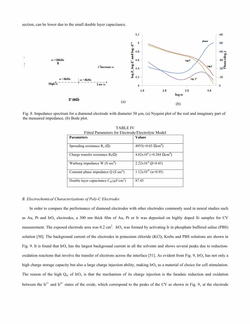
B. Electrochemical Characterizations of Poly-C Electrodes
In order to compare the performance of diamond electrodes with other electrodes commonly used in neural studies such
as Au, Pt and IrOx electrodes, a 300 nm thick film of Au, Pt or Ir was deposited on highly doped Si samples for CV
measurement. The exposed electrode area was 0.2 cm2. IrOx was formed by activating Ir in phosphate buffered saline (PBS)
solution [50]. The background current of the electrodes in potassium chloride (KCl), Krebs and PBS solutions are shown in
Fig. 9. It is found that IrOx has the largest background current in all the solvents and shows several peaks due to reduction-
oxidation reactions that involve the transfer of electrons across the interface [51]. As evident from Fig. 9, IrOx has not only a
high charge storage capacity but also a large charge injection ability, making IrOx as a material of choice for cell stimulation.
The reason of the high Qin of IrOx is that the mechanism of its charge injection is the faradaic reduction and oxidation
between the Ir3+ and Ir4+ states of the oxide, which correspond to the peaks of the CV as shown in Fig. 9, at the electrode
surface [25]. Poly-C, on the other hand, shows no peak and the lowest background current among the materials. This is an
advantage-especially for electrochemical detection because its surface is chemically inert and stable.
IrOx
Au
Pt
Diamond
Cur
rent
Den
sity
(µA
/cm
2 )
Voltage (V)
1 M KCl
(a)
IrOx
Au
Pt
Diamond
Cur
rent
Den
sity
(µA
/cm
2 )
Voltage (V)
Krebs
(b)
IrOx
Au
Pt
Diamond
Cur
rent
Den
sity
(µA
/cm
2 )
Voltage (V)
PBS: Phosphate Buffered Saline
(c)
Fig. 9. Voltammograms of Au, Pt, IrOx and diamond electrodes in (a) 1MKCl, (b) Krebs, and (c) PBS.
In addition to low background current, poly-C electrodes also exhibit a wide water potential window. As shown in Fig.
10(a), the diamond site on the probe reveals a potential window from -0.8 to 1.4 V in 1M KCl, which indicates a high over-
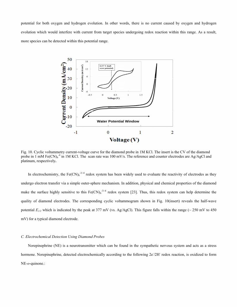
potential for both oxygen and hydrogen evolution. In other words, there is no current caused by oxygen and hydrogen
evolution which would interfere with current from target species undergoing redox reaction within this range. As a result,
more species can be detected within this potential range.
Water Potential Window
0.377 V (half-wave potential)
Fig. 10. Cyclic voltammetry current-voltage curve for the diamond probe in 1M KCl. The insert is the CV of the diamond probe in 1 mM Fe(CN)6
-4 in 1M KCl. The scan rate was 100 mV/s. The reference and counter electrodes are Ag/AgCl and platinum, respectively.
In electrochemistry, the Fe(CN)6-3/-4 redox system has been widely used to evaluate the reactivity of electrodes as they
undergo electron transfer via a simple outer-sphere mechanism. In addition, physical and chemical properties of the diamond
make the surface highly sensitive to this Fe(CN)6-3/-4 redox system [23]. Thus, this redox system can help determine the
quality of diamond electrodes. The corresponding cyclic voltammogram shown in Fig. 10(insert) reveals the half-wave
potential E1/2 which is indicated by the peak at 377 mV (vs. Ag/AgCl). This figure falls within the range (~ 250 mV to 450
mV) for a typical diamond electrode.
C. Electrochemical Detection Using Diamond Probes
Norepinephrine (NE) is a neurotransmitter which can be found in the sympathetic nervous system and acts as a stress
hormone. Norepinephrine, detected electrochemically according to the following 2e-/2H- redox reaction, is oxidized to form
NE-o-quinone.:
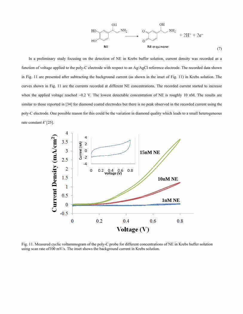
(7) In a preliminary study focusing on the detection of NE in Krebs buffer solution, current density was recorded as a
function of voltage applied to the poly-C electrode with respect to an Ag/AgCl reference electrode. The recorded data shown
in Fig. 11 are presented after subtracting the background current (as shown in the inset of Fig. 11) in Krebs solution. The
curves shown in Fig. 11 are the currents recorded at different NE concentrations. The recorded current started to increase
when the applied voltage reached ~0.2 V. The lowest detectable concentration of NE is roughly 10 nM. The results are
similar to those reported in [34] for diamond coated electrodes but there is no peak observed in the recorded current using the
poly-C electrode. One possible reason for this could be the variation in diamond quality which leads to a small heterogeneous
rate constant ko [25].
15nM NE
10nM NE
1nM NE
Fig. 11. Measured cyclic voltammogram of the poly-C probe for different concentrations of NE in Krebs buffer solution using scan rate of100 mV/s. The inset shows the background current in Krebs solution.
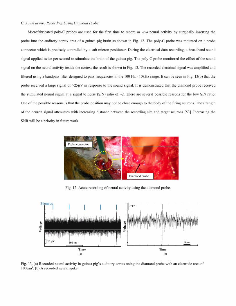
C. Acute in vivo Recording Using Diamond Probe
Microfabricated poly-C probes are used for the first time to record in vivo neural activity by surgically inserting the
probe into the auditory cortex area of a guinea pig brain as shown in Fig. 12. The poly-C probe was mounted on a probe
connector which is precisely controlled by a sub-micron positioner. During the electrical data recording, a broadband sound
signal applied twice per second to stimulate the brain of the guinea pig. The poly-C probe monitored the effect of the sound
signal on the neural activity inside the cortex; the result is shown in Fig. 13. The recorded electrical signal was amplified and
filtered using a bandpass filter designed to pass frequencies in the 100 Hz - 10kHz range. It can be seen in Fig. 13(b) that the
probe received a large signal of >25µV in response to the sound signal. It is demonstrated that the diamond probe received
the stimulated neural signal at a signal to noise (S/N) ratio of ~2. There are several possible reasons for the low S/N ratio.
One of the possible reasons is that the probe position may not be close enough to the body of the firing neurons. The strength
of the neuron signal attenuates with increasing distance between the recording site and target neurons [53]. Increasing the
SNR will be a priority in future work.
Diamond probe
Probe connector
Fig. 12. Acute recording of neural activity using the diamond probe.
10 ms
25 µV
Vol
tage
Time (a) (b)
10 µV 500 ms
Fig. 13. (a) Recorded neural activity in guinea pig’s auditory cortex using the diamond probe with an electrode area of 100µm2, (b) A recorded neural spike.
5. CONCLUSIONS
For the first time, the design, fabrication and testing of a novel polycrystalline diamond (poly-C) based microprobe is
reported for possible applications in neural prosthesis. The probe utilizes undoped poly-C with a resistivity in the range of 105
Ωcm as a mechanical material, which has a young’s modulus in the range of 400 – 1,000 GPa and is biocompatible. Boron
doped poly-C with a resistivity in the range of 10-3 Ωcm is used as an electrode material, which provides a chemically stable
surface for both chemical and electrical detections in neural studies. The probe has eight poly-C electrode sites with
diameters ranging from 2 to 150 µm; the electrode capacitance is approximately 87 µF/cm2. The measured water potential
window of the poly-C electrode spans across negative and positive electrode potentials and typical has a total value of 2.2 V
in 1M KCl; the lowest detectable concentration of norepinephrine was on the order of 10 nM. The poly-C probe has also been
successfully implanted in the auditory cortex area of guinea pig brain for in vivo neural studies. The recorded signal
amplitude was 30-40 µV and had a duration of 1ms.
ACKNOWLEDGEMENT
This work is supported by the Engineering Research Centers Program (ERC) of the National Science Foundation under
Award Number EEC-9986866. The authors are indebted to Ken Wise for his continue support and critical reading of the
manuscript. The authors are thankful to Mike Varney and Sean Hatch for helpful discussion related to work reported in this
paper.
REFERENCES
[1] K. D. Wise, J. B. Angell and A. Starr, “An integrated-circuit approach to extracellular microelectrodes,” IEEE Trans. Biomed. Eng.,
v.17, no. 3, pp. 238-247, 1970.
[2] P. Norlin, M. Kindlundh, A. Mouroux, K. Yoshida and U. G. Hofmann, “A 32-site neural recording probe fabricated by DRIE of SOI
substrates,” J. of Micromech.& Microeng., pp. 414-419, 2002.
[3] D. R. Kipke, “Implantable neural probe systems for cortical neuroprosthesis,” in Proc. of Int. Conf. of the IEEE Eng. in Med. and Bio.
Soc., pp. 5344-5347, 2004.
[4] Q. Bai and K. D. Wise, “Single-unit neural recording with active microelectrode arrays,” IEEE Trans. Biomed. Eng., v. 48, pp. 911-
920, 2001.
[5] C. Pang, J. G. Cham, Z. Nenadic, S. Musallam, Y. C. Tai, J. W. Burdick and R. A. Andersen, “ A new multi-site probe array with
monolithically integrated parylene flexible cable for neural prostheses,” in Proc. of Int. Conf. of the IEEE Eng. in Med. and Bio. Soc.,
pp. 7114- 7117, 2005.
[6] J. Chen and K. D. Wise, “A multichannel neural probe for selective chemical delivery at the cellular level,” IEEE Tans. Biomed Eng.,
v. 44, no. 8, pp. 760-769, 1997.
[7] L. Lin and A. Pisano, “Silicon processed microneedles,” IEEE J. Micromech. Syst., v. 8, no. 1, pp. 78-84, 1999.
[8] J. Wang, M. Gulari, P. T. Bhatti, B. Y. Arcand, K. Beach, C. R. Fredrich and K. D. Wise,, “A cochlear electrode array with built-in
position sensing,” in Proc. of Int. Conf. on MEMS, pp. 786-789, 2005.
[9] Y. Tang, D. M. Aslam, J. Wang and K. D. Wise, “Poly-Crystalline diamond piezoresistive position sensors for cochlear implant
probe,” in Proc. of Solid-State Sensors, Actuators and Microsystems, v.1, pp. 542-546, 2005.
[10] Y. Yao, M. N. Gulari, J. A. Wiler and K. D. Wise, “A microassembled low-profile three-dimensional microelectrode array for neural
prosthesis applications”, J. of Micro. Mech. Syst., v. 16, no. 4, pp. 977-988, 2007.
[11] C. Pang, J. G. Cham, Z. Nenadic, Y. C. Tai, J. W. Burdick and R. A. Andersen, “A new neural recording electrode array with parylene
insulating layer,” in Proc. of Int. Conf. on Miniaturized Syst. for Chemistry and Life Sciences, pp. 675-677, 2005.
[12] E. Patrick, M. Ordonez, N. Alba, J. C. Sanchez and T. Nishida, “Design and fabrication of a flexible substrate microelectrode array for
brain machine interfaces,” in Proc. of IEEE EMBS, pp. 2966-2969, 2006.
[13] Y. Kato, M. Nishino, I. Saito, T. Suzuki and K. Mabuchi, “Flexible intracortical neural probe with biodegradable polymer for
delivering bioactive components,” in Proc. of IEEE EMBS, pp. 143-146, 2006.
[14] S. Takeuchi, T. Suzuki, K. Mabuchi and H. Fujita, “3D flexible multichannel neural probe array,” J. Micomech. Microeng., v. 14, pp.
104-107, 2004.
[15] H. Lu, S. H. Cho, J. B. Lee, L. Cauller, M. R. Ortega and G. Hughes, “SU8-based micro neural probe for enhanced chronic in-vivo
recording of spike signals from regenerated axons,” in Proc. of IEEE Int. Conf. on Sensors, pp. 66-69, 2006.
[16] M. D. Johnson, R. K. Franklin, K. A. Scott, R. B. Brown and D. R. Kipke, “Neural probes for concurrent detection of neurochemical
and electrophysiological signals in vivo,” in Proc. of IEEE EMBS, pp. 7325-7328, 2005.
[17] K. L. Drake, K. D. Wise, J. Farraye, D. J. Anderson and S. P. Bement, “Performance of planar multisite microprobes in recording
extracelluar single-unit intracortical activity,” IEEE Trans. on biomedical eng., v. 35, no. 9, pp. 719-732, 1988.
[18] T. L. Rose, E. M. Kelliher and L. S. Robbless, “Assessment of capacitor electrodes: preliminary evaluation,” J. of Neurosci. Methods,
no. 12, pp. 181-193, 1985.
[19] D. J. Anderson, K. Najafi, S. J. Tanghe, D. A. Evans, K. L. Levy, J. F. Hetke, X. Xue, J. J. Zappia and K. D. Wise, “Batch-fabricated
thin-film electrodes for stimulation of the central auditory system,” IEEE Trans. of Bio. Eng., v. 36, no. 7, 1989.
[20] M. P. Hughes, K. Bustamante, D. J. Banks and D. J. Ewims, “Effects of electrode size on the performance of neural recording
microelectrodes,” in Proc. of IEEE Conf. on Microtech. in Med. And Bio., pp. 220-223, 2000.
[21] J. A. Stamford, P. Palij, C. Davidson, C. M. Jorm and J. Millar, “Simultaneous ‘real time’ electrochemical and electrophysiological
recording in brain slices with a single carbon-fibre microelectrode,” J. of Neuroscience Methods, v. 50, pp. 279-290, 1993.
[22] L. S. Pan, D. R. Kania, Diamond: electronic properties and applications, Springer, 1994.
[23] M. Hupert, A. Muck, J. Wang, J. Stotter, Z. Cvackova, S. Haymond, Y. Show and G. M. Swain, “Conductive diamond thin-films in
electrochemistry,” Dia. and Rel. Mat., v. 12, pp. 1940-1949, 2003.
[24] A.N. Ndao, F. Zenia, A. Deneuville, M. Bernard, C. L. le´ment, “Effect of boron concentration on the electrochemical reduction of
nitrates on polycrystalline diamond electrodes, “ Dia. and Rel. Mat., v. 9, pp. 1175-1180, 2000.
[25] A. Bennett, J. Wang, Y. Show and G. M. Swain, “Effect of sp2-bonded nondiamond carbon impurity on the response of boron-doped
polycrystalline diamond thin-film electrodes,” J. of Electrochem. Soc., v. 151, no. 9, pp. 306-313, 2004.
[26] C. E. Nebel, H. Kato, B. Rezek, D. Shin, D. Takeuchi, H. Watanabe and T. Yamamoto, “Electrochemical properties of undoped
hydrogen terminated CVD diamond,” Dia. and Rel. Mat., v. 15, pp. 264-268, 2006.
[27] G. M. Swain and R. Ramesham, “The electrochemical activity of boron-doped polycrystalline diamond thin film electrode,” Anal.
Chem., v. 65, pp. 345-351, 1993.
[28] L. Tang, C. Tsai, W. W. Gerberich, L. Kruckeberg and D. R. Kania, “Biocompatibility of chemical-vapour-deposited diamond,”
Biomaterials, v. 16, pp. 483-488, 1995.
[29] R. A Freitas, Nanomedicine, Vol. IIA: Biocompatibility, Landes Bioscience, 2003.
[30] E. W. Salzman, J. Linden, G. McManama and J. A. Ware, “Role of fibrinogen in activation of platelets by artificial surfaces,” Annals
N. Y. Acad. Sci, v. 516, pp. 184-195, 1987.
[31] A. Kraft, “Doped diamond: A compact review on a new, versatile, electro material,” Int. J. Electrochem. Sci., v. 2, pp. 355-385,
2007.
[32] J. Cvacka, V. Quaiserova, J. W. Park, Y. Show, A. Muck and G. M. Swain, “Boron-doped diamond microelectrodes for use in
capillary electrophoresis with electrochemical detection,” Anal. Chem., v.75, pp. 2678-2687, 2005.
[33] J. M. Halpern, S. Xie, G. P. Sutton, B. T. Higashikubo, C. A. Chestek, H. Liu H. J. Chiel, and H. B. Martin, “Diamond electrodes for
neurodynamic studies in Aplysia californica,” Dia. and Rel. Mat., v. 15, pp. 183-187, 2006.
[34] J. Park, V. Q. Mocko, K. Peckova, J. J. Galligan, G. D. Fink and G. M. Swain, “ Fabrication, characterization, and application of a
diamond microelectrode for electrochemical measurement of norepinephrine release from the sympathetic nervous system,” Dia. and
Rel. Mat., v. 15, pp. 761-772, 2006.
[35] L. S. Pan and D. R. Kania, Diamond: electronic properties and applications, Springer, 1994.
[36] H. Liu and D. S. Dandy, “Studies on nucleation process in diamond CVD: an overview of recent developments,” Dia. and Rel. Mat.,
v. 4, no. 10, pp. 1173-1188, 1995.
[37] Y. Tang and D. M. Aslam, “Technology of polycrystalline diamond thin films for microsystems applications,” J. Vac. Sci. Technol., v.
3, pp. 1088-1095, 2005.
[38] K. Hermansson, U. Kindberg, B. Hok, G. Palmskoq, “Wetting properties of silicon surfaces,” in Proc. of IEEE Int. Conf. on Solid-
State Sensors and Actuators, pp. 193-196, 1991.
[39] Y. Ando, Y. Niishibayashi, K. Kobashi, T. Hirao and K. Oura, “Smooth and high-rate reactive ion etching of diamond,” Dia. and Rel.
Mat., v. 11, pp. 824-827, 2002.
[40] I. Bell, M. K. Fung, W.J Zhang, K. H. Lai, Y. M. Wang, Z. F. Zhou, R. K. W. Yu, C. S. Lee and S. T. Lee, “Effects at reactive ion
etching of CVD diamond,” Thin Solid Films, v. 368, pp. 222-226, 2000.
[41] G. F. Ding, H. P. Mao, Y. L. Cao, Y. H. Zhang, X. Yao and X. L. Zhao, “Micromachining of CVD diamond by RIE for MEMS
applications,” Dia. and Rel. Mat., v. 14, pp. 1543-1548, 2005.
[42] O. Dorsch, M. Werner and E. Obermeier, “Dry etching of undoped and boron doped polycrystalline diamond films,” Dia. and Rel.
Mat., v. 4, pp. 456-459, 1995.
[43] Z. L. Cao, H. Y. Chan and D. M. Aslam, “Polycrystalline diamond technology in micropackaging,” in preparation.
[44] H. –Y. Chan, D. M. Aslam, S. Wang, G. M. Swain and K. D. Wise, “Fabrication and testing of a novel all-diamond neural probe for
chemical detection and electrical sensing applications,” in Proc. of Int. Conf. on MEMS, pp. 244-247, 2008.
[45] J. E. B. Randles, “Kinetics of rapid electrode reactions. Part 3. – electron exchange reactions,” KW Somerton Trans. of the Faraday
Society, v. 48, pp. 937-950, 1952.
[46] A. J. Bard and L. R. Faulkner, Electrochemical methods: fundamentals and applications, Wiley Publishers, 2000.
[47] J. Xu, Q. Chen and G. M. Swain, “Anthraquinonedisulfonate electrochemistry: A comparison of glassy carbon, hydrogenated glassy
carbon, highly oriented pyrolytic graphite, and diamond electrodes,” Anal. Chem., v. 70, pp. 3146-3154, 1998.
[48] R. Ramesham and M. F. Rose, “Cyclic voltammetric, a. c. and d. c. polarization behavior of boron-doped CVD diamond,” Thin Solids
Films, v. 300, pp. 144-153, 1997.
[49] A. Fujishma, Y. Einaga, T. N. Rao and D. A. Tryk, Diamond electrochemistry, Elsevier, 2005.
[50] J. D. Weiland, “Electrochemical properties of iridium oxide stimulating electrodes,” Ph.D. dissertation, University of Michigan, 1997.
[51] L. S. Robbless, J. L. Lefko and S. B. Brummer, “Activated Ir: An electrode suitable for reversible charge injection in saline solution,”
J. Electrochem. Soc., v. 130, no. 3, pp. 731-732, 1983.
[52] J. Mozota and B. E. Cnway, “Surface and bulk process at oxidized iridium electrodes – I. Monolayer stage and transition to reversible
multilayer oxide film behavior,” Electrochim. Acta, v. 28, pp. 1-8, 1983.
[53] V. S. Polikov, P. A. Tresco, W. M. Reichert, “Response of brain tissue to chronically implanted neural electrodes,” J. of Neuroscience
Method, v. 148, pp. 1-18, 2005.


![Neuro Assessment for Scalp the Non-Neuro Nurse … · Neuro Assessment for the Non-Neuro Nurse Terry M. Foster, RN, ... Microsoft PowerPoint - Neuro Grand Forks ND [Read-Only] Author:](https://img.pdfslide.us/doc/110x75/5b88746b7f8b9a301e8d8c76/neuro-assessment-for-scalp-the-non-neuro-nurse-neuro-assessment-for-the-non-neuro.jpg)