Embed Size (px)
Citation preview

A Novel Design of Reversible Logic based 1-Bit and
4-Bit ALU
Nayana D.K
Research Scholar
Jain University, Bangalore, India.
E-Mail: [email protected]
Sujatha B.K
Prof.: Dept. of Telecommunication Engg.
MSRIT, Bangalore, India
Abstract— in last few years, the concept called Reversible
logic (RL) has received more attention because of its several
abilities like minimizing the power dissipation. Generally, the
more power dissipation will take place in low powered digital
designs. The applicability of RL has extended in several areas like
design of low power CMOS, DNA computing, advanced
computing, quantum computing, processing of optical
information and in nanotechnology. In case of traditional digital
circuits designs the major amount of power loss take place during
the logic operation by which some information bits will be erased.
Thus, in order to protect this information bits from erasing; the
logic gates are needed to be designed. Generally, in reversible
computation the information bits will not be erased. This concept
of reversible computation gives the hint for design of RL gates.
The Central Processing Unit (or CPU) has got a fundamental
building block called as Arithmetic logic Unit (or ALU). The use
of reversible ALU in a computing system can offer higher power
optimization. The realization of arithmetic operations can be
done by adopting proper control logic over any one input
variable parallel to adder. In this paper, 1 bit reversible and 4bit
ALU is presented by using RL. The designed ALU's are analyzed
over the FPGA SPARTAN6 device. The performance of the
proposed mechanism is compared with other existing mechanism
by considering the parameters like garbage outputs, propagation
delay and quantum cost.
Keywords- Arithmetic Logic Unit, central processing unit
(CPU), Reversible logic, FPGA.
I. INTRODUCTION
In design of digital circuits, the energy dissipation is always
an biggest concern. One of the reasons connected to the power
dissipation in digital circuit is technical non-ideality of the
materials and switches. Generally, the logic operations which
performed over the traditional digital circuit designs lead
higher energy dissipation, information bits loss and heat loss.
Thus in order to overcome these issues related to the digital
designs, several fabrication, reverse computation and
integration mechanism are exist. The use of reversible
computation can provide the protection against the loss of
information bits and also minimize the power dissipation. The
logic of reversible computation has planted the development
of reversible logic (RL). Thus, since last decade the reversible
logic has given promise to resolve the power dissipation
issues. The RL has applicability in various application sectors
like design of low power CMOS, DNA computing, advanced
computing, quantum computing, processing of optical
information and in nanotechnology. The non use of RL
concept or use of irreversible hardware computation will lead
in loss of energy because of information bits loss/erase. The
researcher Launderer have suggested that the energy
dissipation in irreversible bit operation will be KT(ln
(2))Joules, where K is Boltzmann's constant and its value is
1.38065x10⁻²³K(joule/Kelvin-1) and T is the temperature
during the operation. Also its is says that the energy
dissipation can be controlled or eliminated by making use of
RL forward and backward operation, which means the
reversible computation will produce inputs through outputs
and at any point of computation it can stop and returns to
history [1].
The analyst Bennett demonstrated that the dissipated power
is straightly identified with the number of bits which were
erased during process., furthermore that the computers can be
reversible logically, lessened complexity and at helpful speed
create précised calculations and to keep away from kT(ln2)
joules of energy dissipation in a circuit it ought to be produced
using RLC. For this the circuit must be logically reversible.
Another approach of configuration comes in the field of digital
circuits outlining for restricting the power dispersal. The
device designed by new approach is known as a Reversible
Logic Device (RLD). An entryway designed utilizing RL is
called Reversible Logic Gate (RLG). Inputs are dictated by the
programmers for execution in a guideline set architecture. In
view of this input number of ALU to have the capacity to
produce assortment of logic outputs. Consequently in this sort
of environment RLC must have both settled select input lines
that get opcode signals controlled by programmed and output
lines where the logical output result is delivered [2].
RLG is an inputI - OutputO logic function. A
RLG is also defined as a bijective Boolean function from I to
O values. Let the input vector be vectorinputPv ,
vectoroutputQv and they are defined as follows,
),.....,( 11 Iiiv PPPP
),,.....,( 11 IIiiv QQQQQ
This will satisfy relation
)vv QP
International Journal of Scientific & Engineering Research, Volume 8, Issue 3, March-2017 ISSN 2229-5518
75
IJSER © 2017 http://www.ijser.org
IJSER

In the design of RLG the below points are necessary.
Low Garbage outputs
Low delay.
There should not be feedbacks or loops
There should not be Fan out
Low quantum cost.
Reversible
Logic
Circuit
P1
P2
Pn
P1
P2
Pn
Fig.1. Reversible Logic gate (RLG) with inputI
and
OutputO
The paper is organized as follows section II highlights prior
research work pertaining to Reversible ALU. Section III
describes problems explored after reviewing the literatures.
Discussion of the proposed system using novel approach is
given in section IV. The Section V will demonstrate the
outcomes of the proposed study followed by Conclusion of
paper in section VI.
II. RELATED WORK
Our earlier survey has as of now talked about different
existing framework to Design of Reversible Logic ALU
utilizing RLG [3] with an unmistakable depiction of the
exploration crevice.
This segment, we audit some more significant research
work towards RL ALU. In Zhijin Guan et al. [4] a plan
building the ALU in view of RLG as rationale segments is
proposed. The exhibited reversible ALU lessens the
information bits' utilization and misfortune by reusing the
rationale information bits logically and understands the
objective of bringing down power utilization.
In Gopal et al. [5] paper, two sorts of reversible ALU
outlines are proposed and checked utilizing Altera Quartus II
programming. In the proposed outlines, eight number juggling
and four logical operations are performed. In the proposed
plan 1, Peres Full Adder Gate (PFAG) is utilized as a part of
reversible ALU outline and HNG door is utilized as a viper
rationale circuit in the proposed ALU outline 2. Both proposed
plans are dissected and looked at as far as number of
entryways check, junk output, quantum cost and spread
postponement. The reproduction results demonstrate that the
proposed reversible ALU outline 2 out forms the proposed
reversible ALU plan 1 and ordinary ALU plan.
In this survey of Praveen Kumar [6] have explored that
the Programmable RL is developing as a forthcoming RL for
usage in quantum computing and cutting edge nanotechnology
with insignificant effect on circuit warm era.
Premanand and Ravindranath [7] portrayed the plan of
programmable RLG structures, focused for the ALU execution
using an effective reversible ALU. Utilizing reversible
rationale doors rather than customary rationale AND/OR
entryways, a reversible ALU whose capacity is the same as
conventional ALU is developed. Contrasting and the input bits
and the lost of bits of the conventional ALU, the reversible
ALU essentially decrease the utilization and loss of
information bits. Programmable RLG are acknowledged in
Verilog HDL, reproduced and orchestrated utilizing Cadence
NCSIM and RTL complier.
Hence, it can be observed that different techniques being
introduced in recent time for evolving up with new strategies
of reversible logic ALU. All the techniques discussed have
significant beneficial point of learn and adopt while associated
with limitations and constraints too. The problems pertaining
to existing studies are discussed briefly in next section.
III. PROBLEM DESCRIPTION
This section presents the problems that have been identified
after reviewing the existing techniques on RL in ALU. It has
been found that focuses of existing techniques on RL in ALU
are quite less. Design of a control unit for any figuring unit is
the hardest part and includes more basic limitations. Power
consumption is a critical issue in VLSI designs. The
progression in VLSI designs and especially compact gadget
advances and progressively high computation necessities,
prompt to the design of speedier, small and more perplexing
electronic Systems. The coming of multi-giga-hertz
processors, top of the line electronic devices carry with them
an expansion in framework complexity, packets with high
density and a issue on power consumption. Hence, the next
section discusses about proposed system to overcome this
issues.
IV. PROPOSED FRAMEWORK
The design of 1-bit ALU and 4-bit ALU utilizing reversible
logical gate is simulated using Verilog. The realized ALU is
examined on FPGA device. This work is compared in terms of
quantum cost, the propagation delay and the garbage outputs.
Here, we designed a 4-bit reversible logic ALU and also the
implementation on proposed 1-bit reversible ALU
architecture. The main part of the ALU is the parallel adder. It
is designed with a many number of full adders and also the
projected 1-bit as well as the 4-bit reversible ALU and it also
uses DKFG gate is used as a full adder by calculating the
inputs to the parallel adder. It is probably to obtain the
different type of ALU operations. The carry input Cin is
applied to the full adder circuit in the lower bit position and it
International Journal of Scientific & Engineering Research, Volume 8, Issue 3, March-2017 ISSN 2229-5518
76
IJSER © 2017 http://www.ijser.org
IJSER

exits the Cout as of the adder. The full adder is used to obtain
the sum of gets and carry output.
The functional expression of an ALU is given by
i
iii
iiiiii
iiiiiii
i
ii
CSZi
BSBSY
BSSSAXbygivenareZandYXWhere
ZXZYYXCandXF
2
10
102
1
,,
1-bit ALU
1
1
A
B
Ci
S0
S1
S2
1F
Count
4-bit ALU
4
4
A
B
Ci
S0
S1
S2
4F
Count
Fig.2. Top Module
Proposed
Control Unit 1
1
1
A0
B0
Ci
S0
S1
S2
DKFG 1
F0
0
C0
Fig.3. Top Module
Figure 2.Shows the block diagram of proposed 1-bit as well
as 4-bit ALU model. It contains the three select inputs such as
S1, S2 and S3. Where, the Ai, Bi and Ci are the 3 different
inputs. Zi, Yi and Xi are the output obtained from proposed
control unit. These signals are given to the DKFG full adder
circuit to perform the summing operations. Fi and Cout are the
two output obtained from full adder circuit. Table 1 shows the
truth table of the proposed 1-bit ALU model.
Form this section we can conclude that, the delay, garbage
value and the quantum cost obtained in 4-bit ALU is more
than 1-bit ALU. The projected ALUs has mainly two most
significant advantages. Firstly, it obtains less propagation
delay is compared with existing 1-bit architecture. As a result,
the novel and newly developed ALU has a best delay for n-bit
ALUs operations. Secondly, the work of ALU generates more
number of arithmetical as well as logical operations. The
projected ALU is well designed and it is flexible that, any type
of alterations actions required for simulation in instruction
data set architecture will be made easy.
Proposed
Control Unit 1
4
4
A0
B0
Ci
S0
S1
S2
DKFG 1
F0
Control Unit 2
A1
B1
C0
S0
S1
S2
DKFG 2
F1
Control Unit 3
4
4
A2
B2
C1
S0
S1
S2
DKFG 3
F2
Control Unit 4
A3
B3
C2
S0
S1
S2
DKFG 4
F3
0
C0
C1
0
0 Count
0
Fig.4. Internal Architecture of 4-bit reversible ALU
Fig.5. Proposed Control Unit for ALU
Table.1.The truth table of the proposed method
International Journal of Scientific & Engineering Research, Volume 8, Issue 3, March-2017 ISSN 2229-5518
77
IJSER © 2017 http://www.ijser.org
IJSER

V. RESULTS AND DISCUSSION
A. Results of 1-bit ALU
The simulated 1-bit as well as 4-bit ALU framework
illustrated and demonstrated in the previous part is
amalgamated and simulated on Xilinx. The 1-bit ALU top
module is shown in fig.6. It having three inputs such as a, b,
cin. Then the select line input is take as s1, s2 and s3
respectively. The output of this module is cout and function.
Fig.6. ALU_1-bit_top_module
The RTL diagram proposed 1-bit ALU as show in figure. 6.
It is the inbuilt architect ere of the 1-bit ALU module.
Similarly, the technological schematic 1 bit ALU diagram
shown in fig.7. This shows the design and development of the
1-bit ALU using Verilog software.
Fig.7. ALU_1-bit_rtl
Fig.8. ALU_1-bit_technology_schematic
The simulated results also shown in fig.9. This process uses
the following elements for the simulation purposes. This
proposed method uses the Artix-7 as a FPGA circuit, it also
uses a device like XC7A100T and Xc7a100t-3csf324 device,
the package is CSG324 and the speed of the device is -3. It
calculate the number of gate count, number of garbage and
number of constant input is given to this simulation work.
Fig.9. ALU_1-bit_Simualtion
The summery of the device utilization values are estimated
as shown in table. 1. It gives the usage of the devices for
simulation work. The number of slice of LUTs is used as 2
and the available is 63,400. Similarly, the number of fully
utilized LUT-FF pairs is zero and the available is 2. And
finally, the number of bonded IOBs is used 8 and the available
is 210. So, the utilization bonded IOBs are 3%, remaining are
International Journal of Scientific & Engineering Research, Volume 8, Issue 3, March-2017 ISSN 2229-5518
78
IJSER © 2017 http://www.ijser.org
IJSER
0%. The target device is xc7a100t-3csg324, the version of
product is ISE 14.7 and it uses the Xilinx by default tool.
Table.2. Device utilization summary
From this 1-bit ALU design we can observed that, the
maximum combination path delay is 1.075ns.
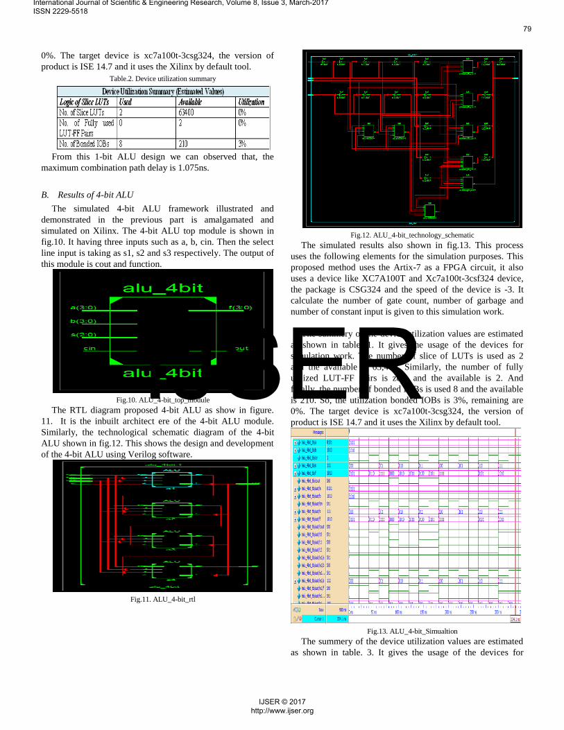
B. Results of 4-bit ALU
The simulated 4-bit ALU framework illustrated and
demonstrated in the previous part is amalgamated and
simulated on Xilinx. The 4-bit ALU top module is shown in
fig.10. It having three inputs such as a, b, cin. Then the select
line input is taking as s1, s2 and s3 respectively. The output of
this module is cout and function.
Fig.10. ALU_4-bit_top_module
The RTL diagram proposed 4-bit ALU as show in figure.
11. It is the inbuilt architect ere of the 4-bit ALU module.
Similarly, the technological schematic diagram of the 4-bit
ALU shown in fig.12. This shows the design and development
of the 4-bit ALU using Verilog software.
Fig.11. ALU_4-bit_rtl
Fig.12. ALU_4-bit_technology_schematic
The simulated results also shown in fig.13. This process
uses the following elements for the simulation purposes. This
proposed method uses the Artix-7 as a FPGA circuit, it also
uses a device like XC7A100T and Xc7a100t-3csf324 device,
the package is CSG324 and the speed of the device is -3. It
calculate the number of gate count, number of garbage and
number of constant input is given to this simulation work.
The summery of the device utilization values are estimated
as shown in table. 1. It gives the usage of the devices for
simulation work. The number of slice of LUTs is used as 2
and the available is 63,400. Similarly, the number of fully
utilized LUT-FF pairs is zero and the available is 2. And
finally, the number of bonded IOBs is used 8 and the available
is 210. So, the utilization bonded IOBs is 3%, remaining are
0%. The target device is xc7a100t-3csg324, the version of
product is ISE 14.7 and it uses the Xilinx by default tool.
Fig.13. ALU_4-bit_Simualtion
The summery of the device utilization values are estimated
as shown in table. 3. It gives the usage of the devices for
International Journal of Scientific & Engineering Research, Volume 8, Issue 3, March-2017 ISSN 2229-5518
79
IJSER © 2017 http://www.ijser.org
IJSER

simulation work. The number of slice of LUTs is used as 8
and the available is 63,400. Similarly, the number of fully
utilized LUT-FF pairs is zero and the available is 8. And
finally, the number of bonded IOBs is used 17 and the
available is 210. So, the utilization bonded IOBs are 8%,
remaining is 0%. The target device is xc7a100t-3csg324, the
version of product is ISE 14.7 and it uses the Xilinx by default
tool.
Table.3. Device utilization summary
From this 4-bit ALU design we can observed that, the
maximum combination path delay is 3.466 ns.
Table.4. Evaluation among the projected reversible 1-bit and 4-bit ALU
Schemes with the present 1- bit ALU proposal
Table 4 gives the comparison between the projected 1-bit
and 4-bit ALU using reversible logic circuit as well as the
existing ALU results.
VI. CONCLUSION
The programmable RLG have been examined in reversible
ALU. These new ALU designs are profitable to existing work
in usage that support low delay and high logical output, which
is attractive for acknowledgment of a reversible CPU. The
proposed plans can be incorporated in the outline of an n-bit
reversible ALU. In this paper examination and investigation
done on gates on FPGA SPARTAN6 device. With the above
investigation it can likewise be determined that proposed 1-Bit
ALU has less postponement than the current 1-Bit ALU. From
this we can observed that our proposed method gives better and
good performance results. The propagation delay, the quantum
cost and finally the garbage outputs are deliberated as the
performance parameters. For conventional RLC there exists
much research, even entire books, performed to the outline and
simulation of computer arithmetic. This is unquestionably not
the situation for RL. The requirement that the circuits must be
garbage-free is the thing that makes it a fascinating exploration
issue, however most proposed designs still actualize the
conventional algorithms with garbage. In this utilized the RLG,
however as their sole objective is to decrease logic size or
number of garbage-bits for a particular fixed size circuit; next
better results are obtained from this approach.
VII. REFERENCES
[1] M. Morrison, N. Ranganathan, “Design of a Reversible ALU
Based on Novel Programmable Reversible Logic Gate
Structures”, VLSI (ISVLSI), IEEE Computer Society Annual
Symposium, pp.126,131, 2013
[2] A. Roohi, H. Khademolhosseini, S. Sayedsalehi, K. Navi,
“Implementation of reversible logic design in nanoelectronics on
basis of majority gates”, Computer Architecture and Digital
Systems (CADS), 2012 16th CSI International Symposium,
pp.1,6, 2012
[3] S. Sharma, S.B. Singh, S. Akashe, “Optimized power
performance and simulation of reversible logic multiplexer”,
Emerging Research Areas and 2013 International Conference
on Microelectronics, Communications and Renewable Energy
(AICERA/ICMiCR), Annual International Conference, pp.1,6,
2013
[4] Z. Guan, “An arithmetic logic unit design based on reversible
logic gates”, Communications, Computers and Signal
Processing (PacRim), IEEE Pacific Rim Conference, 2011
[5] L. Gopal, “Design and synthesis of reversible arithmetic and
Logic Unit (ALU)”, Computer, Communications, and Control
Technology (I4CT), 2014 International Conference, 2014.
[6] P. Kumar, P. Gour, and B.B. Soni, “An Extensive Survey:
Designing of ALU Using Reversible Logic Gates”, International
Journal of Emerging Technology and Advanced Engineering,
Vol. 4 (6), 2014
[7] B. Premananda, and Y. M. Rravindhranath, “Design and
synthesis of 16 bit ALU using reversible logic gates”, Int. J.
Adv. Res. Commun. Eng, Vol.2.10, pp. 2278-1021, 2013
International Journal of Scientific & Engineering Research, Volume 8, Issue 3, March-2017 ISSN 2229-5518
80
IJSER © 2017 http://www.ijser.org
IJSER