Embed Size (px)
Citation preview
Abstract—A novel coupled-inductor switched-capacitor
inverter (CISCI) is proposed by combining a non-overlapping
circuit and sinusoidal pulse-width-modulation (SPWM)
controller for the high-gain boost DC-AC conversion and
closed-loop regulation. The power part is composed of two
cascaded sub-circuits, including: (i) a booster with coupled-
inductor and switched-capacitor (one coupled-inductor, 2
pumping capacitor, and one switch controlled by a non-
overlapping circuit), and (ii) a half-bridge DC-link inverter (2
capacitors and 2 switches controlled by SPWM), so as to obtain
an AC range: +((2+n+nD)/2(1-D))VS~ -((2+n+nD)/2(1-D))VS,
where D is the duty cycle and n is the turn ratio of
coupled-inductor. Practically, the maximum output voltage can
reach 12.5 times voltage of source VS while D=0.5, n=8. Here,
the SPWM is employed to enhance regulation capability for the
different output amplitude and frequency, as well as robustness
to source/loading variation. Finally, the closed-loop CISCI is
designed and simulated by OrCAD SPICE for some cases:
steady-state and dynamic responses. All results are illustrated
to show the efficacy of the proposed scheme.
Index Terms—coupled-inductor switched-capacitor inverter,
high-gain boost, DC-AC conversion, sinusoidal pulse-width-
modulation.
I. INTRODUCTION
ecently years, due to the popularity of mobile devices,
e.g. digital camera, e-book, smart phone, notebook, and
pad …etc., the power modules of these products always ask
for some good characteristics: small volume, light weight,
higher efficiency, and better regulation capability. Generally,
the traditional power converters have a large volume and a
heavy weight because of magnetic elements. Therefore, more
manufactures and researchers pay much attention to this topic,
and ultimately, requiring DC-DC/DC-AC step-up/down
converters realized on a compact chip by mixed-mode VLSI
technology.
The switched-capacitor (SC) power converter has
received more and more attention because it has only
semiconductor switches and capacitors. Thus, this kind of SC
converters is one of the good solutions for low-power and
high-gain DC-DC/DC-AC conversion. Up to now, the
various SC types have been suggested for power conversion.
Manuscript received December 5, 2015. This work is supported in part by
Ministry of Science and Technology of Taiwan, R.O.C., under Grant MOST
104-2221-E-324-015.
Yuen-Haw Chang and Jyun-Jia Liao are with the Department and
Graduate Institute of Computer Science and Information Engineering,
Chaoyang University of Technology, Taichung, Taiwan, R.O.C. Post code:
413. (e-mail: [email protected], [email protected]).
In 1976, Dickson charge pumping was proposed based on a
diode-chain structure via pumping capacitors [1]. In 1990s,
Ioinovici proposed a SC with two capacitor cells working
complementarily, as well as current-mode SC [2][3]. In 2007,
Chang proposed a CPLD-based implementation of SC
step-down DC-DC converter for multiple output choices [4].
In 2011-2013, Chang et al. proposed a series of multistage/
multiphase SC step-up/down DC-DC/DC-AC converter/
inverter [5-8]. In 2013, Chang et al. proposed a 2-stage
4-phase switched-capacitor boost DC-AC inverter with
sinusoidal PFM control [9]. In 2014, Chang et al. proposed a
closed-loop high-gain switched-capacitor-inductor-based
boost DC-AC Inverter [10].
In order to reach a higher voltage gain, it is one of the
feasible ways to adopt the device of coupled-inductor.
Nevertheless, the stress on transistors and the volume of
magnetic device could be considered. In 2014, Chen et al.
proposed a coupled-inductor boost integrated flyback
converter including high-voltage gain and ripple-free input
current [11]. Hamid Bahrami et al. suggested a modified
step-up boost converter with coupled-inductor and super-lift
techniques [12]. In 2015, Chen et al. proposed a novel
switched-coupled-inductor DC-DC step-up converter and its
derivatives [13]. Wu et al. proposed a non-isolated high
step-up DC-DC converter adopting switched-capacitor cell
[14]. Based on the above research, the authors make an
attempt on combining SC circuit with one coupled-inductor
to propose a closed-loop CISCI here for a higher gain under a
fewer element count.
II. CONFIGURATION OF CISCI
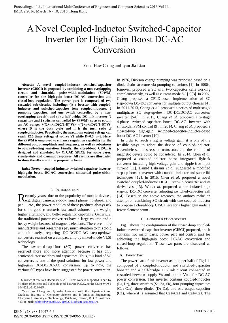
Fig.1 shows the configuration of the closed-loop coupled-
inductor switched-capacitor inverter (CISCI) proposed, and it
contains two major parts: power part and control part for
achieving the high-gain boost DC-AC conversion and
closed-loop regulation. These two parts are discussed as
follows.
A. Power Part
The power part of this inverter as in upper half of Fig.1 is
composed of a coupled-inductor and switched-capacitor
booster and a half-bridge DC-link circuit connected in
cascaded between supply Vs and output Vout for DC-AC
power conversion. This inverter contains coupled-inductor
(L1, L2), three switches (S1, Sa, Sb), four pumping capacitors
(Ca1-Ca4), three diodes (D1-D3), and one output capacitor
(CL), where it is assumed that Ca1=Ca2 and Ca3=Ca4. The
A Novel Coupled-Inductor Switched-Capacitor
Inverter for High-Gain Boost DC-AC
Conversion
Yuen-Haw Chang and Jyun-Jia Liao
R
Proceedings of the International MultiConference of Engineers and Computer Scientists 2016 Vol II, IMECS 2016, March 16 - 18, 2016, Hong Kong
ISBN: 978-988-14047-6-3 ISSN: 2078-0958 (Print); ISSN: 2078-0966 (Online)
IMECS 2016
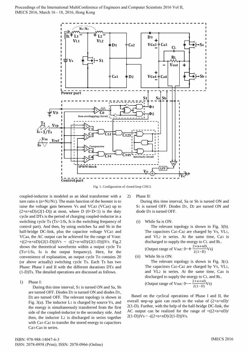
Fig. 1. Configuration of closed-loop CISCI.
coupled-inductor is modeled as an ideal transformer with a
turn ratio n (n=N2/N1). The main function of the booster is to
raise the voltage gain between Vs and VCa3 (VCa4) up to
(2+n+nD)/(2(1-D)) at most, where D (0<D<1) is the duty
cycle and DTs is the period of charging coupled-inductor in a
switching cycle Ts (Ts=1/fs, fs is the switching frequency of
control part). And then, by using switches Sa and Sb in the
half-bridge DC-link, plus the capacitor voltage VCa3 and
VCa4, the AC output can be achieved for the range of Vout:
+((2+n+nD)/(2(1-D)))VS ~ -((2+n+nD)/(2(1-D)))VS. Fig.2
shows the theoretical waveforms within a output cycle To
(To=1/fo, fo is the output frequency). Here, for the
convenience of explanation, an output cycle To contains 20
(or above actually) switching cycle Ts. Each Ts has two
Phase: Phase I and II with the different durations DTs and
(1-D)Ts. The detailed operations are discussed as follows.
1) Phase I:
During this time interval, S1 is turned ON and Sa, Sb
are turned OFF. Diodes D3 is turned ON and diodes D1,
D2 are turned OFF. The relevant topology is shown in
Fig. 3(a). The inductor L1 is charged by source Vs, and
the energy is simultaneously transferred from the first
side of the coupled-inductor to the secondary side. And
then, the inductor L2 is discharged in series together
with Ca1-Ca2 to transfer the stored energy to capacitors
Ca3-Ca4 in series.
2) Phase II:
During this time interval, Sa or Sb is turned ON and
S1 is turned OFF. Diodes D1, D2 are turned ON and
diode D3 is turned OFF.
(i) While Sa is ON:
The relevant topology is shown in Fig. 3(b).
The capacitors Ca1-Ca2 are charged by Vs, VL1,
and VL2 in series. At the same time, Ca3 is
discharged to supply the energy to CL and RL.
(Output range of Vout: 0~
Vs)
(ii) While Sb is ON:
The relevant topology is shown in Fig. 3(c).
The capacitors Ca1-Ca2 are charged by VS, VL1,
and VL2 in series. At the same time, Ca4 is
discharged to supply the energy to CL and RL.
(Output range of Vout: 0~
Vs)
Based on the cyclical operations of Phase I and II, the
overall step-up gain can reach to the value of (2+n+nD)/
2(1-D). Further, with the help of the half-bridge DC-link, the
AC output can be realized for the range of +((2+n+nD)/
2(1-D))Vs ~ -((2+n+nD)/2(1-D))Vs.
Proceedings of the International MultiConference of Engineers and Computer Scientists 2016 Vol II, IMECS 2016, March 16 - 18, 2016, Hong Kong
ISBN: 978-988-14047-6-3 ISSN: 2078-0958 (Print); ISSN: 2078-0966 (Online)
IMECS 2016
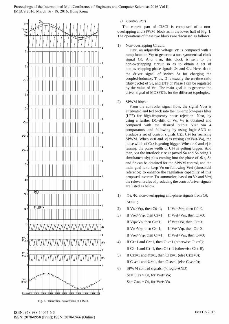
Fig. 2. Theoretical waveforms of CISCI.
B. Control Part
The control part of CISCI is composed of a non-
overlapping and SPWM block as in the lower half of Fig. 1.
The operations of these two blocks are discussed as follows.
1) Non-overlapping Circuit:
First, an adjustable voltage VD is compared with a
ramp function Vrp to generate a non-symmetrical clock
signal C0. And then, this clock is sent to the
non-overlapping circuit so as to obtain a set of
non-overlapping phase signals Φ1 and Φ2. Here, Φ1 is
the driver signal of switch S1 for charging the
coupled-inductor. Thus, D is exactly the on-time ratio
(duty cycle) of S1, and DTS of Phase I can be regulated
by the value of VD. The main goal is to generate the
driver signal of MOSFETs for the different topologies.
2) SPWM block:
From the controller signal flow, the signal Vout is
attenuated and fed back into the OP-amp low-pass filter
(LPF) for high-frequency noise rejection. Next, by
using a further DC-shift of Vc, Vo is obtained and
compared with the desired output Vref via 4
comparators, and following by using logic-AND to
produce a set of control signals C12, C34 for realizing
SPWM. When e>0 and |e| is raising (e=Vref-Vo), the
pulse width of C12 is getting bigger. When e<0 and |e| is
raising, the pulse width of C34 is getting bigger. And
then, via the interlock circuit (avoid Sa and Sb being 1
simultaneously) plus coming into the phase of Φ2, Sa
and Sb can be obtained for the SPWM control, and the
main goal is to keep Vo on following Vref (sinusoidal
reference) to enhance the regulation capability of this
proposed inverter. To summarize, based on Vo and Vref,
the relevant rules of producing the control/driver signals
are listed as below.
1) Φ1, Φ2: non-overlapping anti-phase signals from C0;
S1=Φ1;
2) If VD>Vrp, then C0=1; If VD<Vrp, then C0=0.
3) If Vref>Vrp, then C1=1; If Vref<Vrp, then C1=0;
If Vrp>Vo, then C2=1; If Vrp<Vo, then C2=0;
If Vo>Vrp, then C3=1; If Vo<Vrp, then C3=0;
If Vref>Vrp, then C4=1; If Vref<Vrp, then C4=0;
4) If C1=1 and C2=1, then C12=1 (otherwise C12=0);
If C3=1 and C4=1, then C 34=1 (otherwise C34=0);
5) If C12=1 and Φ2=1, then C12S=1 (else C12S=0);
If C34=1 and Φ2=1, then C34S=1 (else C34S=0);
6) SPWM control signals: (^: logic-AND)
Sa= C12S ^ C0, for Vref>Vo;
Sb= C34S ^ C0, for Vref<Vo.
Proceedings of the International MultiConference of Engineers and Computer Scientists 2016 Vol II, IMECS 2016, March 16 - 18, 2016, Hong Kong
ISBN: 978-988-14047-6-3 ISSN: 2078-0958 (Print); ISSN: 2078-0966 (Online)
IMECS 2016
(a)
(b)
(c)
Fig. 3. Topologies for Phase (a) I, (b) II (Sa:ON), and (b) II (Sb:ON).
III. EXAMPLES OF CISCI
In this paper, the proposed CISCI is simulated by OrCAD,
and all the parameters are listed in TABLE I. There are totally
3 cases for steady-state responses and 4 cases for dynamic
responses respectively. Then, these results are illustrated to
verify the efficacy of the proposed inverter.
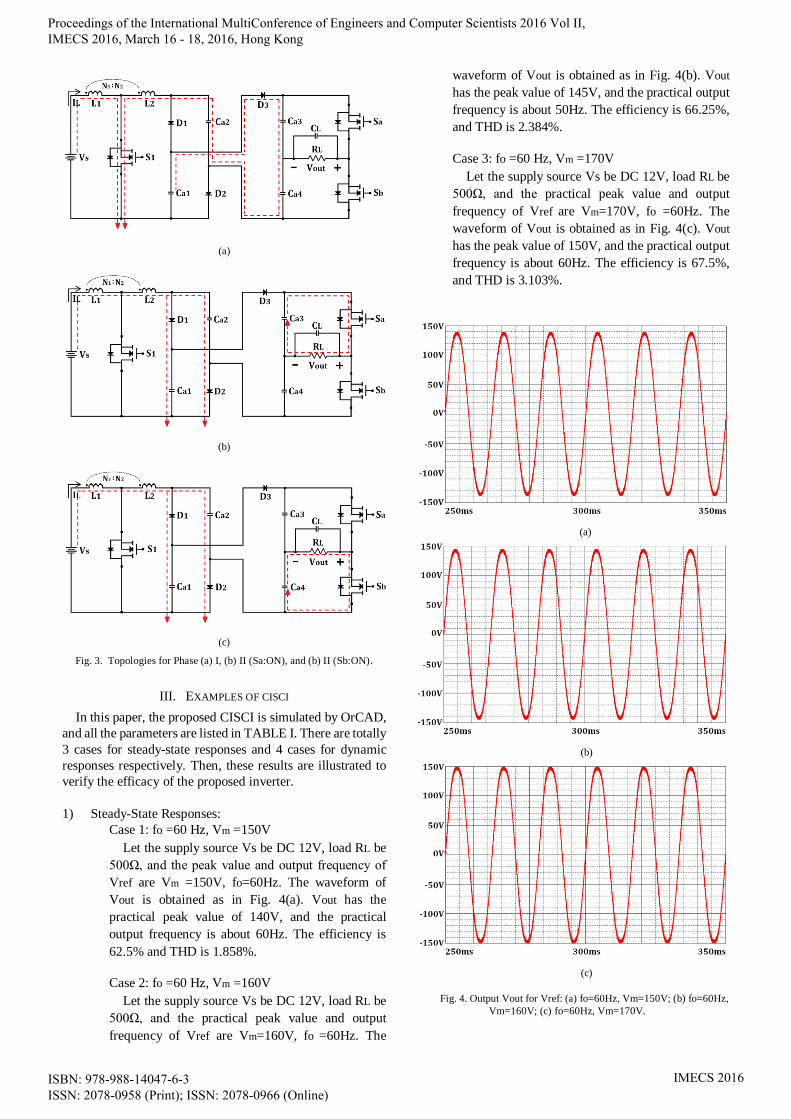
1) Steady-State Responses:
Case 1: fo =60 Hz, Vm =150V
Let the supply source Vs be DC 12V, load RL be
500Ω, and the peak value and output frequency of
Vref are Vm =150V, fo=60Hz. The waveform of
Vout is obtained as in Fig. 4(a). Vout has the
practical peak value of 140V, and the practical
output frequency is about 60Hz. The efficiency is
62.5% and THD is 1.858%.
Case 2: fo =60 Hz, Vm =160V
Let the supply source Vs be DC 12V, load RL be
500Ω, and the practical peak value and output
frequency of Vref are Vm=160V, fo =60Hz. The
waveform of Vout is obtained as in Fig. 4(b). Vout
has the peak value of 145V, and the practical output
frequency is about 50Hz. The efficiency is 66.25%,
and THD is 2.384%.
Case 3: fo =60 Hz, Vm =170V
Let the supply source Vs be DC 12V, load RL be
500Ω, and the practical peak value and output
frequency of Vref are Vm=170V, fo =60Hz. The
waveform of Vout is obtained as in Fig. 4(c). Vout
has the peak value of 150V, and the practical output
frequency is about 60Hz. The efficiency is 67.5%,
and THD is 3.103%.
(a)
(b)
(c)
Fig. 4. Output Vout for Vref: (a) fo=60Hz, Vm=150V; (b) fo=60Hz,
Vm=160V; (c) fo=60Hz, Vm=170V.
Proceedings of the International MultiConference of Engineers and Computer Scientists 2016 Vol II, IMECS 2016, March 16 - 18, 2016, Hong Kong
ISBN: 978-988-14047-6-3 ISSN: 2078-0958 (Print); ISSN: 2078-0966 (Online)
IMECS 2016
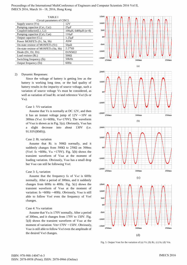
TABLE I Circuit parameters of CISCI.
Supply source (VS) 12V
Pumping capacitor (Ca1, Ca2) 25μF
Coupled-inductor(L1, L2) 100μH, 6400μH (n=8)
Pumping capacitor (Ca3, Ca4) 110μF
Output capacitor (CL) 1.25μF
Power MOSFETs (S1, Sa, Sb) ASW
On-state resistor of MOSFETs (S1) 50μΩ
On-state resistor of MOSFETs (Sa, Sb) 2.275Ω
Diode (D1, D2, D3) D1N5822
Load resistor (RL) 500Ω
Switching frequency (fs) 50kHz
Output frequency (fo) 60Hz
2) Dynamic Responses:
Since the voltage of battery is getting low as the
battery is working long time, or the bad quality of
battery results in the impurity of source voltage, such a
variation of source voltage Vs must be considered, as
well as variation of load RL or/and reference Vref (fo or
Vm).
Case 1: VS variation
Assume that Vs is normally at DC 12V, and then
it has an instant voltage jump of 12V→10V on
300ms (Vref: fO=60Hz, Vm=170V). The waveform
of Vout is shown as in Fig. 5(a). Obviously, Vout has
a slight decrease into about 130V (i.e.
91.93V(RMS)).
Case 2: RL variation
Assume that RL is 500Ω normally, and it
suddenly changes from 500Ω to 250Ω on 300ms
(Vref: fo =60Hz, Vm =170V). Fig. 5(b) shows the
transient waveform of Vout at the moment of
loading variation. Obviously, Vout has a small drop
but Vout can still be following Vref.
Case 3: fO variation
Assume that the frequency fo of Vref is 60Hz
normally, After a period of 300ms, and it suddenly
changes from 60Hz to 40Hz. Fig. 5(c) shows the
transient waveform of Vout at the moment of
variation: fo =60Hz→40Hz. Obviously, Vout is still
able to follow Vref even the frequency of Vref
changes.
Case 4: Vm variation
Assume that Vm is 170V normally, After a period
of 300ms, and it changes from 170V to 150V. Fig.
5(d) shows the transient waveform of Vout at the
moment of variation: Vm=170V→150V. Obviously,
Vout is still able to follow Vref even the amplitude of
the desired Vref changes.
(a)
(b)
(c)
(d)
Fig. 5. Output Vout for the variation of (a) VS; (b) RL; (c) fo; (d) Vm.
Proceedings of the International MultiConference of Engineers and Computer Scientists 2016 Vol II, IMECS 2016, March 16 - 18, 2016, Hong Kong
ISBN: 978-988-14047-6-3 ISSN: 2078-0958 (Print); ISSN: 2078-0966 (Online)
IMECS 2016
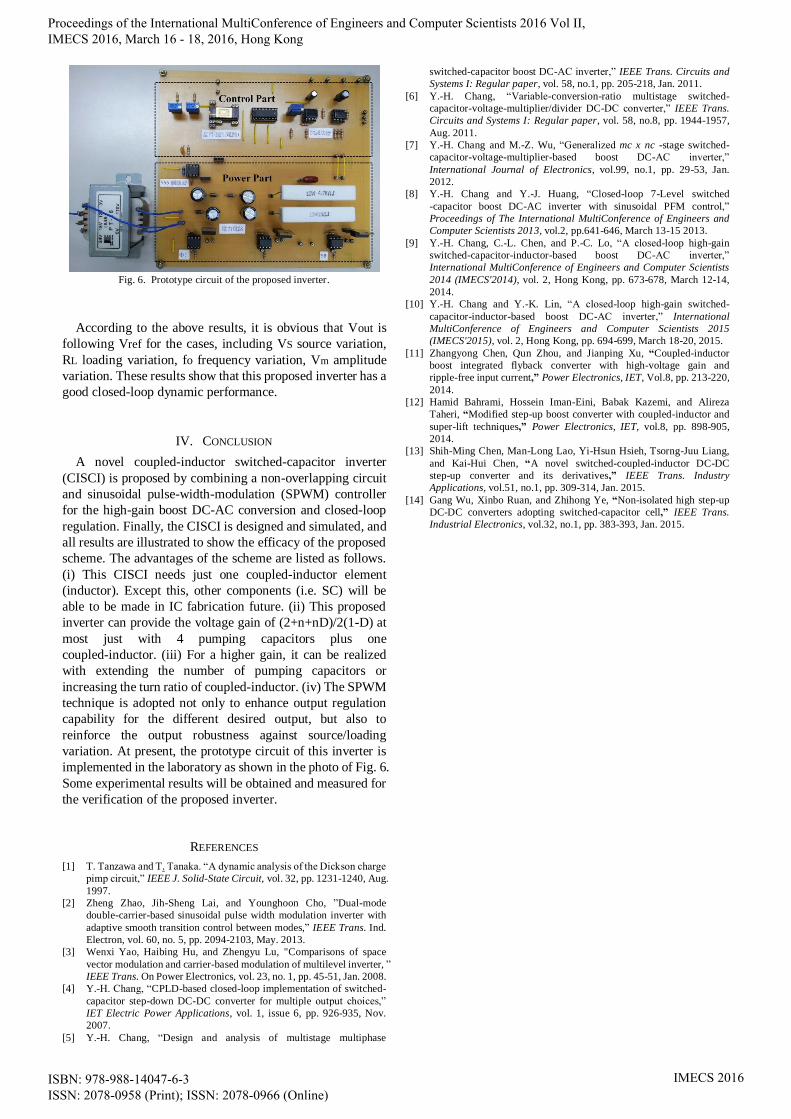
Fig. 6. Prototype circuit of the proposed inverter.
According to the above results, it is obvious that Vout is
following Vref for the cases, including VS source variation,
RL loading variation, fo frequency variation, Vm amplitude
variation. These results show that this proposed inverter has a
good closed-loop dynamic performance.
IV. CONCLUSION
A novel coupled-inductor switched-capacitor inverter
(CISCI) is proposed by combining a non-overlapping circuit
and sinusoidal pulse-width-modulation (SPWM) controller
for the high-gain boost DC-AC conversion and closed-loop
regulation. Finally, the CISCI is designed and simulated, and
all results are illustrated to show the efficacy of the proposed
scheme. The advantages of the scheme are listed as follows.
(i) This CISCI needs just one coupled-inductor element
(inductor). Except this, other components (i.e. SC) will be
able to be made in IC fabrication future. (ii) This proposed
inverter can provide the voltage gain of (2+n+nD)/2(1-D) at
most just with 4 pumping capacitors plus one
coupled-inductor. (iii) For a higher gain, it can be realized
with extending the number of pumping capacitors or
increasing the turn ratio of coupled-inductor. (iv) The SPWM
technique is adopted not only to enhance output regulation
capability for the different desired output, but also to
reinforce the output robustness against source/loading
variation. At present, the prototype circuit of this inverter is
implemented in the laboratory as shown in the photo of Fig. 6.
Some experimental results will be obtained and measured for
the verification of the proposed inverter.
REFERENCES
[1] T. Tanzawa and T. Tanaka. “A dynamic analysis of the Dickson charge
pimp circuit,” IEEE J. Solid-State Circuit, vol. 32, pp. 1231-1240, Aug.
1997.
[2] Zheng Zhao, Jih-Sheng Lai, and Younghoon Cho, ”Dual-mode
double-carrier-based sinusoidal pulse width modulation inverter with
adaptive smooth transition control between modes,” IEEE Trans. Ind.
Electron, vol. 60, no. 5, pp. 2094-2103, May. 2013.
[3] Wenxi Yao, Haibing Hu, and Zhengyu Lu, "Comparisons of space
vector modulation and carrier-based modulation of multilevel inverter, ”
IEEE Trans. On Power Electronics, vol. 23, no. 1, pp. 45-51, Jan. 2008.
[4] Y.-H. Chang, “CPLD-based closed-loop implementation of switched-
capacitor step-down DC-DC converter for multiple output choices,”
IET Electric Power Applications, vol. 1, issue 6, pp. 926-935, Nov.
2007.
[5] Y.-H. Chang, “Design and analysis of multistage multiphase
switched-capacitor boost DC-AC inverter,” IEEE Trans. Circuits and
Systems I: Regular paper, vol. 58, no.1, pp. 205-218, Jan. 2011.
[6] Y.-H. Chang, “Variable-conversion-ratio multistage switched-
capacitor-voltage-multiplier/divider DC-DC converter,” IEEE Trans.
Circuits and Systems I: Regular paper, vol. 58, no.8, pp. 1944-1957,
Aug. 2011.
[7] Y.-H. Chang and M.-Z. Wu, “Generalized mc x nc -stage switched-
capacitor-voltage-multiplier-based boost DC-AC inverter,”
International Journal of Electronics, vol.99, no.1, pp. 29-53, Jan.
2012.
[8] Y.-H. Chang and Y.-J. Huang, “Closed-loop 7-Level switched
-capacitor boost DC-AC inverter with sinusoidal PFM control,”
Proceedings of The International MultiConference of Engineers and
Computer Scientists 2013, vol.2, pp.641-646, March 13-15 2013.
[9] Y.-H. Chang, C.-L. Chen, and P.-C. Lo, “A closed-loop high-gain
switched-capacitor-inductor-based boost DC-AC inverter,”
International MultiConference of Engineers and Computer Scientists
2014 (IMECS'2014), vol. 2, Hong Kong, pp. 673-678, March 12-14,
2014.
[10] Y.-H. Chang and Y.-K. Lin, “A closed-loop high-gain switched-
capacitor-inductor-based boost DC-AC inverter,” International
MultiConference of Engineers and Computer Scientists 2015
(IMECS'2015), vol. 2, Hong Kong, pp. 694-699, March 18-20, 2015.
[11] Zhangyong Chen, Qun Zhou, and Jianping Xu, “Coupled-inductor
boost integrated flyback converter with high-voltage gain and
ripple-free input current,” Power Electronics, IET, Vol.8, pp. 213-220,
2014.
[12] Hamid Bahrami, Hossein Iman-Eini, Babak Kazemi, and Alireza
Taheri, “Modified step-up boost converter with coupled-inductor and
super-lift techniques,” Power Electronics, IET, vol.8, pp. 898-905,
2014.
[13] Shih-Ming Chen, Man-Long Lao, Yi-Hsun Hsieh, Tsorng-Juu Liang,
and Kai-Hui Chen, “A novel switched-coupled-inductor DC-DC
step-up converter and its derivatives,” IEEE Trans. Industry
Applications, vol.51, no.1, pp. 309-314, Jan. 2015.
[14] Gang Wu, Xinbo Ruan, and Zhihong Ye, “Non-isolated high step-up
DC-DC converters adopting switched-capacitor cell,” IEEE Trans.
Industrial Electronics, vol.32, no.1, pp. 383-393, Jan. 2015.
Proceedings of the International MultiConference of Engineers and Computer Scientists 2016 Vol II, IMECS 2016, March 16 - 18, 2016, Hong Kong
ISBN: 978-988-14047-6-3 ISSN: 2078-0958 (Print); ISSN: 2078-0966 (Online)
IMECS 2016