Embed Size (px)
Citation preview
A NOVEL CONCEPT FOR PHASE ERROR CORRECTION IN
SUPERCONDUCTIVE UNDULATORS:
THEORY AND EXPERIMENTAL VERIFICATION
Zur Erlangung des akademischen Grades eines
DOKTORS DER NATURWISSENSCHAFTEN
von der Fakultat Physik der Univeristat (TH)
Karlsruhe
genehmigte
DISSERTATION
von
Dipl.-Ing Daniel Wollmann
aus Dresden
Tag der mundlichen Prufung: 12.12.2008
Referent: Prof. Dr.rer.nat. T. Baumbach
Korreferent: Prof. Dr.rer.nat. G. Quast
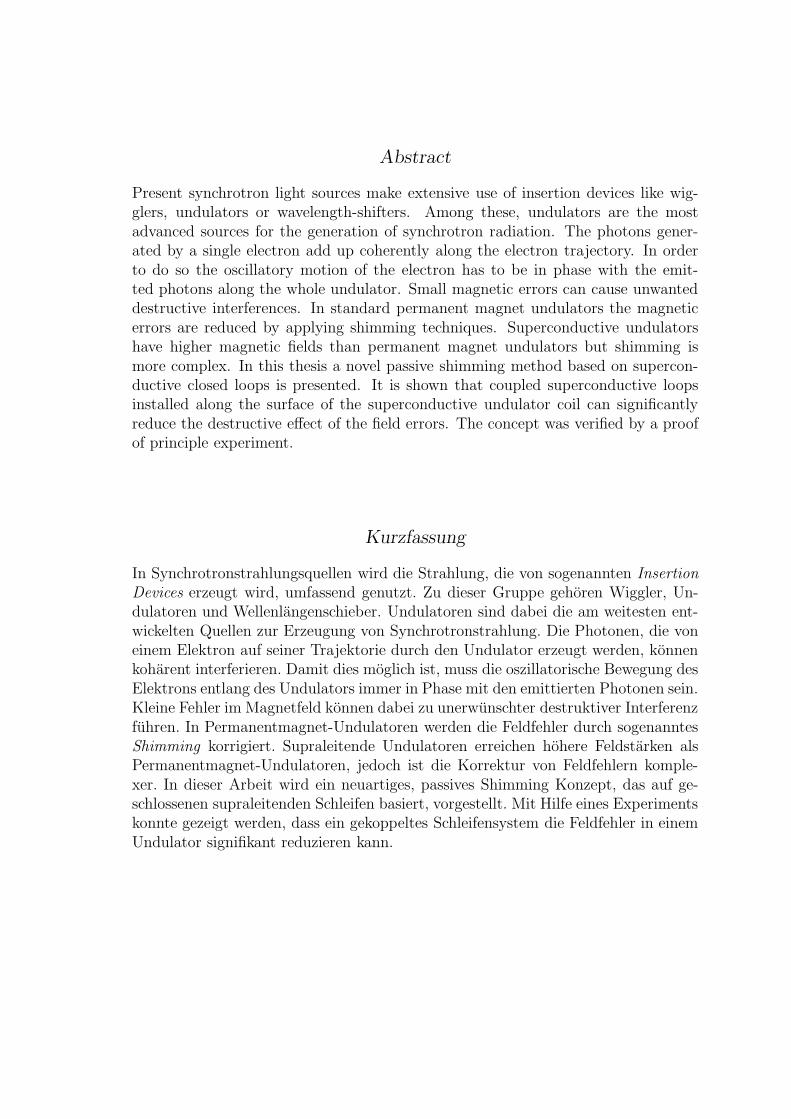
Abstract
Present synchrotron light sources make extensive use of insertion devices like wig-glers, undulators or wavelength-shifters. Among these, undulators are the mostadvanced sources for the generation of synchrotron radiation. The photons gener-ated by a single electron add up coherently along the electron trajectory. In orderto do so the oscillatory motion of the electron has to be in phase with the emit-ted photons along the whole undulator. Small magnetic errors can cause unwanteddestructive interferences. In standard permanent magnet undulators the magneticerrors are reduced by applying shimming techniques. Superconductive undulatorshave higher magnetic fields than permanent magnet undulators but shimming ismore complex. In this thesis a novel passive shimming method based on supercon-ductive closed loops is presented. It is shown that coupled superconductive loopsinstalled along the surface of the superconductive undulator coil can significantlyreduce the destructive effect of the field errors. The concept was verified by a proofof principle experiment.
Kurzfassung
In Synchrotronstrahlungsquellen wird die Strahlung, die von sogenannten Insertion
Devices erzeugt wird, umfassend genutzt. Zu dieser Gruppe gehoren Wiggler, Un-dulatoren und Wellenlangenschieber. Undulatoren sind dabei die am weitesten ent-wickelten Quellen zur Erzeugung von Synchrotronstrahlung. Die Photonen, die voneinem Elektron auf seiner Trajektorie durch den Undulator erzeugt werden, konnenkoharent interferieren. Damit dies moglich ist, muss die oszillatorische Bewegung desElektrons entlang des Undulators immer in Phase mit den emittierten Photonen sein.Kleine Fehler im Magnetfeld konnen dabei zu unerwunschter destruktiver Interferenzfuhren. In Permanentmagnet-Undulatoren werden die Feldfehler durch sogenanntesShimming korrigiert. Supraleitende Undulatoren erreichen hohere Feldstarken alsPermanentmagnet-Undulatoren, jedoch ist die Korrektur von Feldfehlern komple-xer. In dieser Arbeit wird ein neuartiges, passives Shimming Konzept, das auf ge-schlossenen supraleitenden Schleifen basiert, vorgestellt. Mit Hilfe eines Experimentskonnte gezeigt werden, dass ein gekoppeltes Schleifensystem die Feldfehler in einemUndulator signifikant reduzieren kann.
CONTENTS
1. Introduction . . . . . . . . . . . . . . . . . . . . . . . . . . . . . . . . . . . 5
2. Synchrotron Radiation and Insertion Devices . . . . . . . . . . . . . . . . . 72.1 Types of undulators . . . . . . . . . . . . . . . . . . . . . . . . . . . . 102.2 Equations of motion for an electron in an undulator field . . . . . . . 122.3 Synchrotron radiation from undulators . . . . . . . . . . . . . . . . . 142.4 The phase error . . . . . . . . . . . . . . . . . . . . . . . . . . . . . . 17
3. Magnetic field errors caused by finite mechanical tolerances . . . . . . . . . 193.1 Types of mechanical deviations . . . . . . . . . . . . . . . . . . . . . 19
3.1.1 Variation of the pole position . . . . . . . . . . . . . . . . . . 213.1.2 Variation of the wire bundle position . . . . . . . . . . . . . . 223.1.3 Period length variation . . . . . . . . . . . . . . . . . . . . . . 23
3.2 The influence of the undulator current on the different field errors . . 253.3 Decomposition of the measured SCU14 B-field . . . . . . . . . . . . . 26
4. Phase Error and Mechanical Tolerances . . . . . . . . . . . . . . . . . . . . 294.1 Sine wave model . . . . . . . . . . . . . . . . . . . . . . . . . . . . . 294.2 Statistically distributed deviations (Monte-Carlo) . . . . . . . . . . . 314.3 Systematic variations . . . . . . . . . . . . . . . . . . . . . . . . . . . 34
5. Classical shimming methods for superconductive undulators . . . . . . . . 365.1 Mechanical shimming methods . . . . . . . . . . . . . . . . . . . . . . 365.2 Shimming with integral correctors . . . . . . . . . . . . . . . . . . . . 375.3 Active shimming with local correction coils . . . . . . . . . . . . . . . 39
5.3.1 Active in gap shim coils . . . . . . . . . . . . . . . . . . . . . 415.3.2 Active in iron shim coils . . . . . . . . . . . . . . . . . . . . . 435.3.3 Active lateral shim coils . . . . . . . . . . . . . . . . . . . . . 435.3.4 Active lateral shim coils on a laminated undulator . . . . . . . 45
6. Superconductors in magnetic fields . . . . . . . . . . . . . . . . . . . . . . 496.1 Type-I superconductors . . . . . . . . . . . . . . . . . . . . . . . . . . 506.2 Type-II superconductors . . . . . . . . . . . . . . . . . . . . . . . . . 51
6.2.1 Shubnikov phase . . . . . . . . . . . . . . . . . . . . . . . . . 556.2.2 YBCO . . . . . . . . . . . . . . . . . . . . . . . . . . . . . . . 56
Contents 4
7. Induction Shimming: Concept . . . . . . . . . . . . . . . . . . . . . . . . . 587.1 Induction-shimming: Theory . . . . . . . . . . . . . . . . . . . . . . . 58
7.1.1 One period with closed-loop . . . . . . . . . . . . . . . . . . . 587.1.2 Two overlapping closed-loops . . . . . . . . . . . . . . . . . . 597.1.3 Generalization for n closed-loops . . . . . . . . . . . . . . . . 61
7.2 Generalization for Biot-Savart closed-loops . . . . . . . . . . . . . . . 627.2.1 Faraday’s law for overlapping closed-loops in a long undulator 637.2.2 Biot-Savart’s law for overlapping closed-loops in a long undulator 63
7.3 Simulations . . . . . . . . . . . . . . . . . . . . . . . . . . . . . . . . 667.3.1 Correction of a single field-error . . . . . . . . . . . . . . . . . 667.3.2 Monte-Carlo simulations . . . . . . . . . . . . . . . . . . . . . 66
8. Induction Shimming: Experiment . . . . . . . . . . . . . . . . . . . . . . . 718.1 Experimental Setup . . . . . . . . . . . . . . . . . . . . . . . . . . . . 718.2 Results and Interpretation . . . . . . . . . . . . . . . . . . . . . . . . 75
8.2.1 Field correction at 70A . . . . . . . . . . . . . . . . . . . . . . 778.2.2 Reduction of the correction efficiency at the critical current . . 818.2.3 Hysteretic behaviour of the closed loop system at high fields . 85
8.3 Induction-shimming: Outlook . . . . . . . . . . . . . . . . . . . . . . 88
9. Conclusion . . . . . . . . . . . . . . . . . . . . . . . . . . . . . . . . . . . . 90
Appendix 104
A. Phase error derivation . . . . . . . . . . . . . . . . . . . . . . . . . . . . . 105
B. Simulation with Opera-3D . . . . . . . . . . . . . . . . . . . . . . . . . . . 109
1. INTRODUCTION
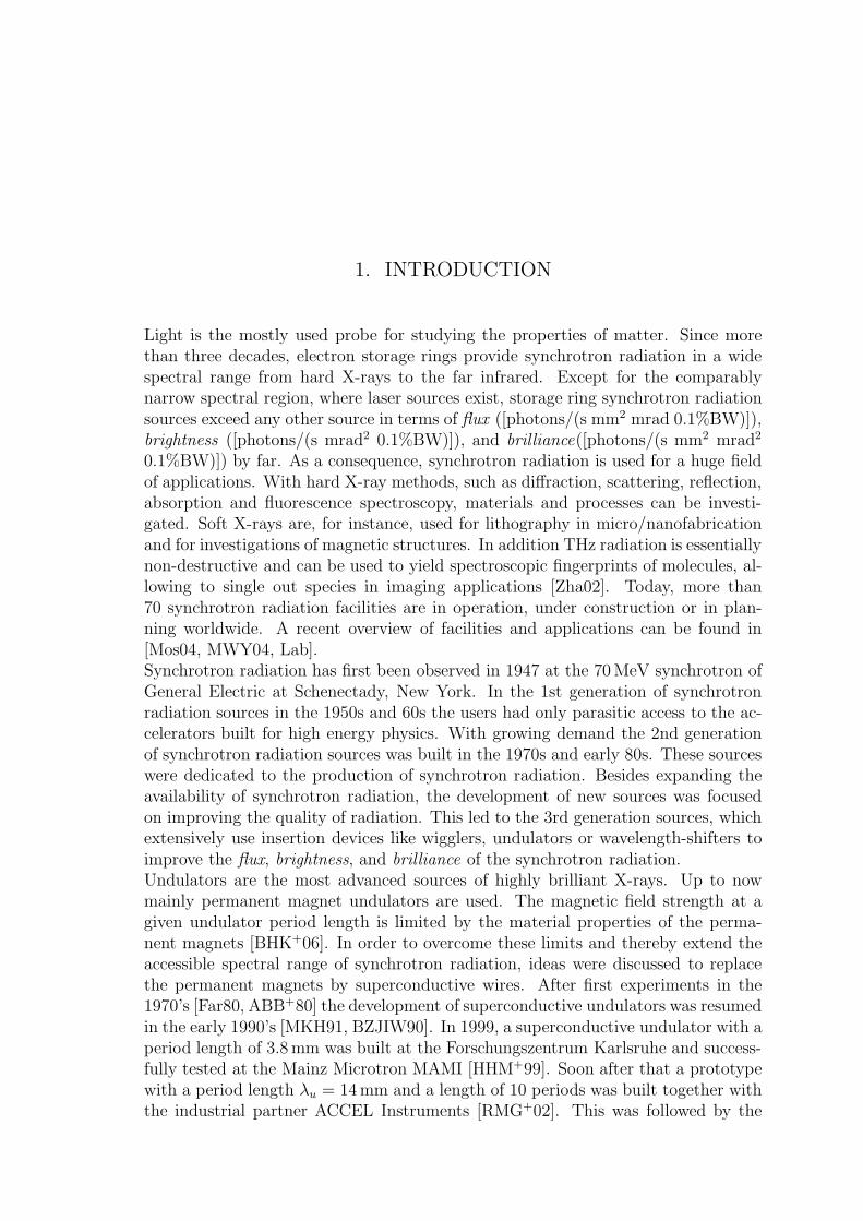
Light is the mostly used probe for studying the properties of matter. Since morethan three decades, electron storage rings provide synchrotron radiation in a widespectral range from hard X-rays to the far infrared. Except for the comparablynarrow spectral region, where laser sources exist, storage ring synchrotron radiationsources exceed any other source in terms of flux ([photons/(s mm2 mrad 0.1%BW)]),brightness ([photons/(s mrad2 0.1%BW)]), and brilliance([photons/(s mm2 mrad2
0.1%BW)]) by far. As a consequence, synchrotron radiation is used for a huge fieldof applications. With hard X-ray methods, such as diffraction, scattering, reflection,absorption and fluorescence spectroscopy, materials and processes can be investi-gated. Soft X-rays are, for instance, used for lithography in micro/nanofabricationand for investigations of magnetic structures. In addition THz radiation is essentiallynon-destructive and can be used to yield spectroscopic fingerprints of molecules, al-lowing to single out species in imaging applications [Zha02]. Today, more than70 synchrotron radiation facilities are in operation, under construction or in plan-ning worldwide. A recent overview of facilities and applications can be found in[Mos04, MWY04, Lab].Synchrotron radiation has first been observed in 1947 at the 70 MeV synchrotron ofGeneral Electric at Schenectady, New York. In the 1st generation of synchrotronradiation sources in the 1950s and 60s the users had only parasitic access to the ac-celerators built for high energy physics. With growing demand the 2nd generationof synchrotron radiation sources was built in the 1970s and early 80s. These sourceswere dedicated to the production of synchrotron radiation. Besides expanding theavailability of synchrotron radiation, the development of new sources was focusedon improving the quality of radiation. This led to the 3rd generation sources, whichextensively use insertion devices like wigglers, undulators or wavelength-shifters toimprove the flux, brightness, and brilliance of the synchrotron radiation.Undulators are the most advanced sources of highly brilliant X-rays. Up to nowmainly permanent magnet undulators are used. The magnetic field strength at agiven undulator period length is limited by the material properties of the perma-nent magnets [BHK+06]. In order to overcome these limits and thereby extend theaccessible spectral range of synchrotron radiation, ideas were discussed to replacethe permanent magnets by superconductive wires. After first experiments in the1970’s [Far80, ABB+80] the development of superconductive undulators was resumedin the early 1990’s [MKH91, BZJIW90]. In 1999, a superconductive undulator with aperiod length of 3.8 mm was built at the Forschungszentrum Karlsruhe and success-fully tested at the Mainz Microtron MAMI [HHM+99]. Soon after that a prototypewith a period length λu = 14 mm and a length of 10 periods was built together withthe industrial partner ACCEL Instruments [RMG+02]. This was followed by the
1. Introduction 6
construction of a 50 period undulator for single pass accelerators (FELs) and, later,by a 100 period undulator for the ANKA storage ring, both with a period length of14 mm. The latter was installed at ANKA in March 2005 [BHK+06, CHK+06]. Itwas shown that a narrow-gap superconductive undulator can be reliably operated ina storage ring under standard user operation conditions [KRH+05]. This so-calledSCU14 was the first superconductive undulator installed in a storage ring. Currentlyan improved superconductive undulator with a period length of 15 mm is under con-struction in collaboration with Babcock Noell GmbH, Wurzburg, Germany, and willbe installed at ANKA in 2009.
The spectral properties of the synchrotron radiation produced by an undulatordepend mainly on the quality of the undulator magnetic field: amplitude and phaseof the magnetic field must be within small tolerances over the complete length of theundulator. The field quality is quantified by the so-called phase error. Techniquesfor phase error correction, the so-called shimming, of permanent magnet undulatorswith magnetized metal strips are state of the art. For superconductive undulatorsshimming with additional superconductive correction coils was proposed and exper-imentally tested [CRS+03, PDB+05, Wol05, WBC+06].
In the first part of this thesis the influence of mechanical tolerances on the phaseerror of superconducting undulators is investigated. In the second part active shim-ming methods to compensate field errors using correction coils are studied. Withthese classical methods shimming is an iterative and time consuming process ofmeasuring, applying shim coils and verifying the improved field quality. In thethird part a novel shimming concept based on superconductive closed-loops is pre-sented [WBR08, WBP+08c, WBP+08b]. This novel concept automatically mini-mizes field errors. The system works in the following way: high temperature super-conductive closed-loops on top of the undulator coils enclose one or several undulatorperiods. In case each of the enclosed poles produces a perfect field (no phase error)the integral magnetic flux through the loops is zero and the induced current into theloop is zero. As soon as the field in one of the poles deviates from its ideal value acurrent is induced in the loop which compensates the field deviation.This concept was verified in a proof of principle experiment and the results of thisexperiment are explained and summarized at the end of this thesis.
2. SYNCHROTRON RADIATION AND INSERTION DEVICES
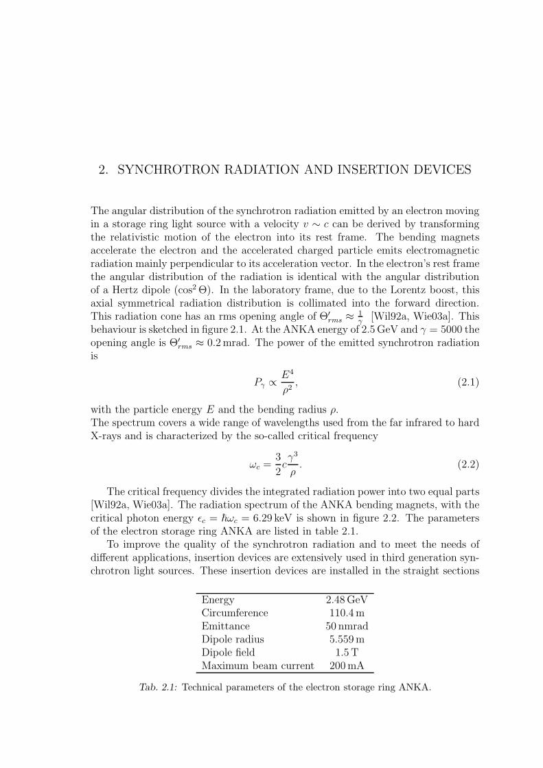
The angular distribution of the synchrotron radiation emitted by an electron movingin a storage ring light source with a velocity v ∼ c can be derived by transformingthe relativistic motion of the electron into its rest frame. The bending magnetsaccelerate the electron and the accelerated charged particle emits electromagneticradiation mainly perpendicular to its acceleration vector. In the electron’s rest framethe angular distribution of the radiation is identical with the angular distributionof a Hertz dipole (cos2 Θ). In the laboratory frame, due to the Lorentz boost, thisaxial symmetrical radiation distribution is collimated into the forward direction.This radiation cone has an rms opening angle of Θ′
rms ≈1γ
[Wil92a, Wie03a]. Thisbehaviour is sketched in figure 2.1. At the ANKA energy of 2.5 GeV and γ = 5000 theopening angle is Θ′
rms ≈ 0.2 mrad. The power of the emitted synchrotron radiationis
Pγ ∝E4
ρ2, (2.1)
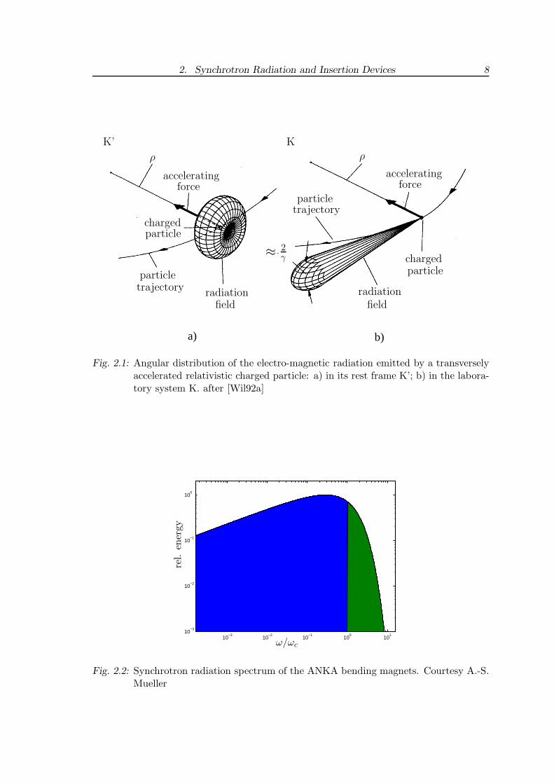
with the particle energy E and the bending radius ρ.The spectrum covers a wide range of wavelengths used from the far infrared to hardX-rays and is characterized by the so-called critical frequency
ωc =3
2cγ3
ρ. (2.2)
The critical frequency divides the integrated radiation power into two equal parts[Wil92a, Wie03a]. The radiation spectrum of the ANKA bending magnets, with thecritical photon energy ǫc = ~ωc = 6.29 keV is shown in figure 2.2. The parametersof the electron storage ring ANKA are listed in table 2.1.
To improve the quality of the synchrotron radiation and to meet the needs ofdifferent applications, insertion devices are extensively used in third generation syn-chrotron light sources. These insertion devices are installed in the straight sections
Energy 2.48 GeVCircumference 110.4 mEmittance 50 nmradDipole radius 5.559 mDipole field 1.5 TMaximum beam current 200 mA
Tab. 2.1: Technical parameters of the electron storage ring ANKA.
2. Synchrotron Radiation and Insertion Devices 8
b)a)
K’ K
ρ ρ
acceleratingacceleratingforce force
charged
charged
particle
particle
particle
particle
trajectory
trajectory
radiation radiationfield field
≈ 2γ
Fig. 2.1: Angular distribution of the electro-magnetic radiation emitted by a transverselyaccelerated relativistic charged particle: a) in its rest frame K’; b) in the labora-tory system K. after [Wil92a]
10−3
10−2
10−1
100
101
10−3
10−2
10−1
100
ω/ωc
rel.
ener
gy
Fig. 2.2: Synchrotron radiation spectrum of the ANKA bending magnets. Courtesy A.-S.Mueller
2. Synchrotron Radiation and Insertion Devices 9
synchrotronradiation
high energyelectrons
dipole magnet
wiggler
undulator
Fig. 2.3: The three main sources for synchrotron radiation: bending magnet (top), wiggler(center), undulator (bottom). Courtesy ESRF.
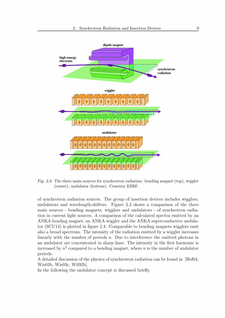
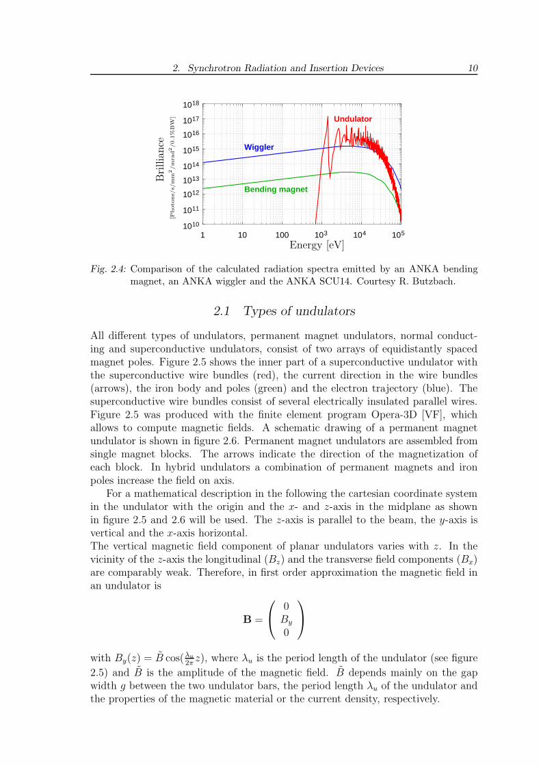
of synchrotron radiation sources. The group of insertion devices includes wigglers,undulators and wavelength-shifters. Figure 2.3 shows a comparison of the threemain sources - bending magnets, wigglers and undulators - of synchrotron radia-tion in current light sources. A comparison of the calculated spectra emitted by anANKA bending magnet, an ANKA wiggler and the ANKA superconductive undula-tor (SCU14) is plotted in figure 2.4. Comparable to bending magnets wigglers emitalso a broad spectrum. The intensity of the radiation emitted by a wiggler increaseslinearly with the number of periods n. Due to interference the emitted photons inan undulator are concentrated in sharp lines. The intensity in the first harmonic isincreased by n2 compared to a bending magnet, where n is the number of undulatorperiods.A detailed discussion of the physics of synchrotron radiation can be found in [Hof04,Wie03b, Wie03c, Wil92b].In the following the undulator concept is discussed briefly.
2. Synchrotron Radiation and Insertion Devices 10
1010
104 105103
1011
1012
1013
1014
1015
1016
1017
Bending magnet
Wiggler
Undulator
1018
1 10 100Energy [eV]
Bri
llia
nce
[Photo
ns/
s/m
m2/m
rad2/0.1
%B
W]
Fig. 2.4: Comparison of the calculated radiation spectra emitted by an ANKA bendingmagnet, an ANKA wiggler and the ANKA SCU14. Courtesy R. Butzbach.
2.1 Types of undulators
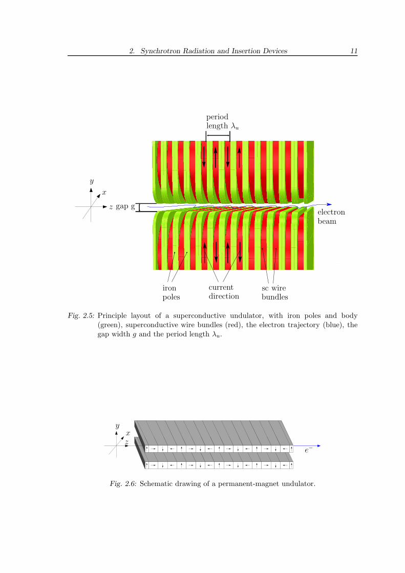
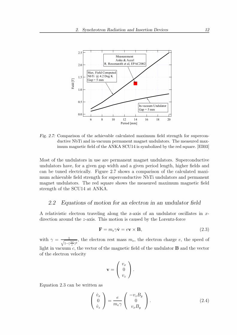
All different types of undulators, permanent magnet undulators, normal conduct-ing and superconductive undulators, consist of two arrays of equidistantly spacedmagnet poles. Figure 2.5 shows the inner part of a superconductive undulator withthe superconductive wire bundles (red), the current direction in the wire bundles(arrows), the iron body and poles (green) and the electron trajectory (blue). Thesuperconductive wire bundles consist of several electrically insulated parallel wires.Figure 2.5 was produced with the finite element program Opera-3D [VF], whichallows to compute magnetic fields. A schematic drawing of a permanent magnetundulator is shown in figure 2.6. Permanent magnet undulators are assembled fromsingle magnet blocks. The arrows indicate the direction of the magnetization ofeach block. In hybrid undulators a combination of permanent magnets and ironpoles increase the field on axis.
For a mathematical description in the following the cartesian coordinate systemin the undulator with the origin and the x- and z-axis in the midplane as shownin figure 2.5 and 2.6 will be used. The z-axis is parallel to the beam, the y-axis isvertical and the x-axis horizontal.The vertical magnetic field component of planar undulators varies with z. In thevicinity of the z-axis the longitudinal (Bz) and the transverse field components (Bx)are comparably weak. Therefore, in first order approximation the magnetic field inan undulator is
B =
0By
0
with By(z) = B cos(λu
2πz), where λu is the period length of the undulator (see figure
2.5) and B is the amplitude of the magnetic field. B depends mainly on the gapwidth g between the two undulator bars, the period length λu of the undulator andthe properties of the magnetic material or the current density, respectively.
2. Synchrotron Radiation and Insertion Devices 11
ironpoles
currentdirection
sc wirebundles
electronbeam
gap g
periodlength λu
x
y
z
Fig. 2.5: Principle layout of a superconductive undulator, with iron poles and body(green), superconductive wire bundles (red), the electron trajectory (blue), thegap width g and the period length λu.
e−
xy
z
Fig. 2.6: Schematic drawing of a permanent-magnet undulator.
2. Synchrotron Radiation and Insertion Devices 12
Superconductive 14 mm Period Undulators , EPAC 02,
R. Rossmanith, H. O. Moser, A. Geisler, A. Hobl, D. Krischel, M. Schillo,
2.5
2.0
1.5
1.0
0.5
0.0
Fie
ld [
T]
20181614121086
Period [mm]
Max. Field ComputedNbTi @ 4.2 Deg K
Gap = 5 mm
Measurement
Anka & AccelR. Rossmanith et al, EPAC2002
In-vacuum Undulator
Gap = 5 mm
1.0
0.5
0.0
-0.5
-1.0
Maxim
um
fir
ld [
T] a
t 1
00
0 A
300250200150100
Position [mm]
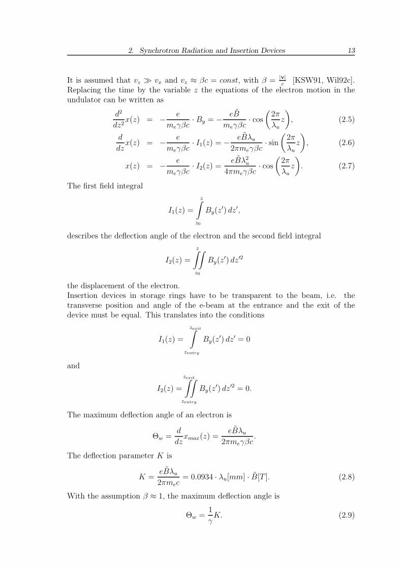
Fig. 2.7: Comparison of the achievable calculated maximum field strength for supercon-ductive NbTi and in-vacuum permanent magnet undulators. The measured max-imum magnetic field of the ANKA SCU14 is symbolized by the red square. [Ell03]
Most of the undulators in use are permanent magnet undulators. Superconductiveundulators have, for a given gap width and a given period length, higher fields andcan be tuned electrically. Figure 2.7 shows a comparison of the calculated maxi-mum achievable field strength for superconductive NbTi undulators and permanentmagnet undulators. The red square shows the measured maximum magnetic fieldstrength of the SCU14 at ANKA.
2.2 Equations of motion for an electron in an undulator field
A relativistic electron traveling along the z-axis of an undulator oscillates in x-direction around the z-axis. This motion is caused by the Lorentz-force
F = meγv = ev × B, (2.3)
with γ = 1q
1−(|v|c
)2, the electron rest mass me, the electron charge e, the speed of
light in vacuum c, the vector of the magnetic field of the undulator B and the vectorof the electron velocity
v =
vx
0vz
.
Equation 2.3 can be written as
vx
0vz
=e
meγ
−vzBy
0vxBy
. (2.4)
2. Synchrotron Radiation and Insertion Devices 13
It is assumed that vz ≫ vx and vz ≈ βc = const, with β = |v|c
[KSW91, Wil92c].Replacing the time by the variable z the equations of the electron motion in theundulator can be written as
d2
dz2x(z) = −
e
meγβc· By = −
eB
meγβc· cos
(
2π
λuz
)
, (2.5)
d
dzx(z) = −
e
meγβc· I1(z) = −
eBλu
2πmeγβc· sin
(
2π
λu
z
)
, (2.6)
x(z) = −e
meγβc· I2(z) =
eBλ2u
4πmeγβc· cos
(
2π
λuz
)
. (2.7)
The first field integral
I1(z) =
z∫
z0
By(z′) dz′,
describes the deflection angle of the electron and the second field integral
I2(z) =
z∫∫
z0
By(z′) dz′2
the displacement of the electron.Insertion devices in storage rings have to be transparent to the beam, i.e. thetransverse position and angle of the e-beam at the entrance and the exit of thedevice must be equal. This translates into the conditions
I1(z) =
zexit∫
zentry
By(z′) dz′ = 0
and
I2(z) =
zexit∫∫
zentry
By(z′) dz′2 = 0.
The maximum deflection angle of an electron is
Θw =d
dzxmax(z) =
eBλu
2πmeγβc.
The deflection parameter K is
K =eBλu
2πmec= 0.0934 · λu[mm] · B[T ]. (2.8)
With the assumption β ≈ 1, the maximum deflection angle is
Θw =1
γK. (2.9)
2. Synchrotron Radiation and Insertion Devices 14
Θ = Kγ
λu
A
2γ
particletrajectory
x
z
NN SS
Fig. 2.8: Trajectory of an electron passing through the magnetic field of an undulator andemitting light into the forward direction.Parameters are: the deflection parameter K, the maximum deflection angle Θw,the maximum electron displacement A and the relativistic factor γ.
By definition the maximum deflection angle of an electron in an undulator is rela-tively small compared to other insertion devices like wigglers [Mue05]. With K ≈ 1this yields
Θw ∼1
γ.
Therefore light is emitted into a narrow forward cone. Figure 2.8 illustrates theelectron trajectory, the deflection parameter K, the maximum deflection angle Θw
and the emitted light cone with an opening angle of 1/γ [KSW91, Wil92c, Mue05,OE03].
2.3 Synchrotron radiation from undulators
The radiation emitted along the trajectory of an electron overlaps and can interfere[Jac99a, Hof04]. As a result an undulator emits a line spectrum, which is given bythe undulator equation
λL =λu
2kγ2
(
1 +K2
2+ Θ2γ2
)
. (2.10)
k is the number of the harmonic and Θ the observation angle. It is important to note,that on axis, i.e. Θ = 0, only odd harmonics are observed (k = 1, 3, 5, ...). Outside
2. Synchrotron Radiation and Insertion Devices 15
0 2 4 6 8 10 120
1
2
3
4
5
6
7x 10
14
Energy [keV]
Flu
x [P
hoto
ns/s
/mm
2 /0.1
%B
W]
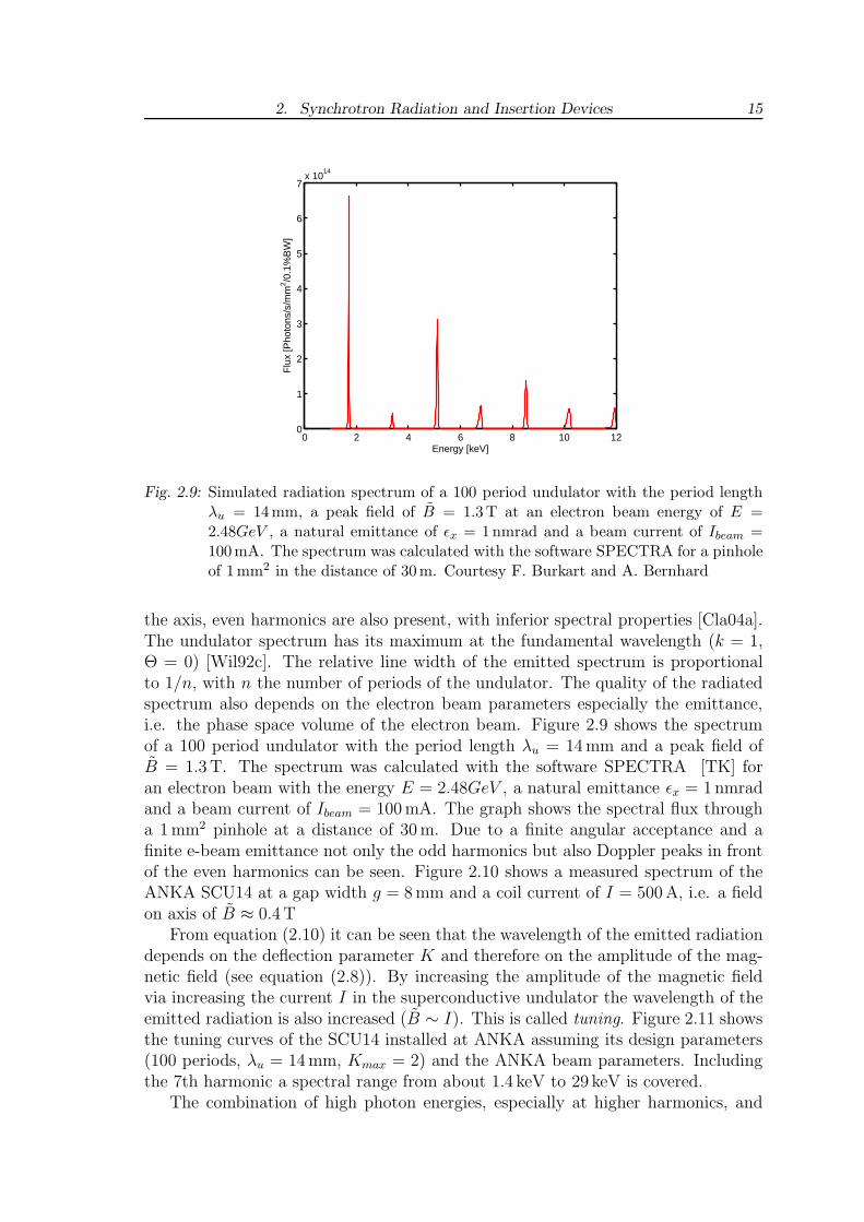
Fig. 2.9: Simulated radiation spectrum of a 100 period undulator with the period lengthλu = 14mm, a peak field of B = 1.3T at an electron beam energy of E =2.48GeV , a natural emittance of ǫx = 1nmrad and a beam current of Ibeam =100mA. The spectrum was calculated with the software SPECTRA for a pinholeof 1mm2 in the distance of 30m. Courtesy F. Burkart and A. Bernhard
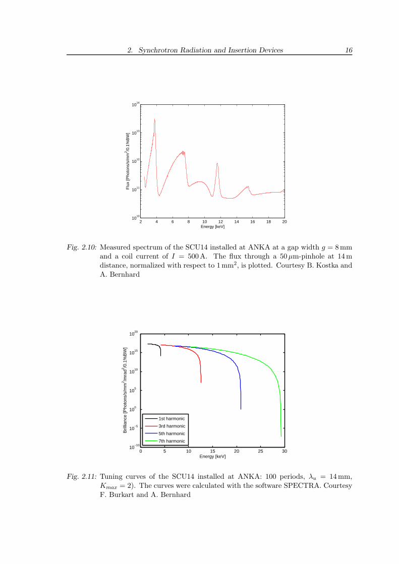
the axis, even harmonics are also present, with inferior spectral properties [Cla04a].The undulator spectrum has its maximum at the fundamental wavelength (k = 1,Θ = 0) [Wil92c]. The relative line width of the emitted spectrum is proportionalto 1/n, with n the number of periods of the undulator. The quality of the radiatedspectrum also depends on the electron beam parameters especially the emittance,i.e. the phase space volume of the electron beam. Figure 2.9 shows the spectrumof a 100 period undulator with the period length λu = 14 mm and a peak field ofB = 1.3 T. The spectrum was calculated with the software SPECTRA [TK] foran electron beam with the energy E = 2.48GeV , a natural emittance ǫx = 1 nmradand a beam current of Ibeam = 100 mA. The graph shows the spectral flux througha 1 mm2 pinhole at a distance of 30 m. Due to a finite angular acceptance and afinite e-beam emittance not only the odd harmonics but also Doppler peaks in frontof the even harmonics can be seen. Figure 2.10 shows a measured spectrum of theANKA SCU14 at a gap width g = 8 mm and a coil current of I = 500 A, i.e. a fieldon axis of B ≈ 0.4 T
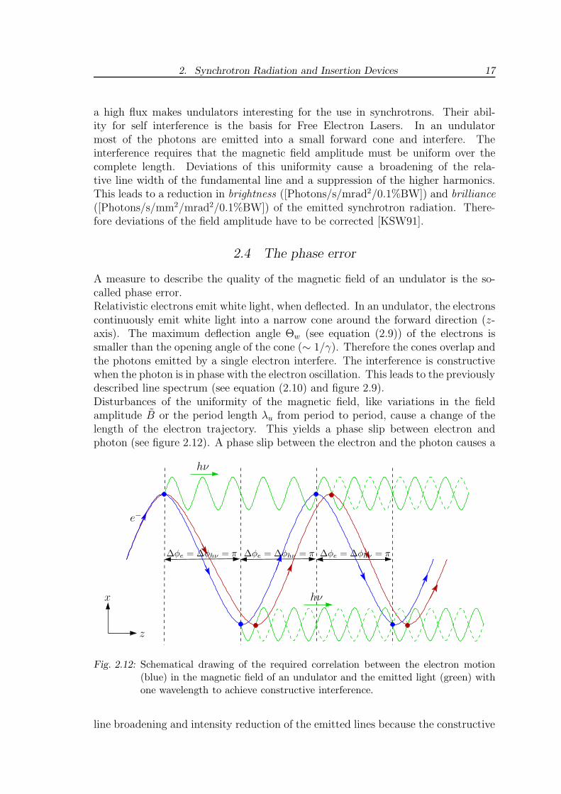
From equation (2.10) it can be seen that the wavelength of the emitted radiationdepends on the deflection parameter K and therefore on the amplitude of the mag-netic field (see equation (2.8)). By increasing the amplitude of the magnetic fieldvia increasing the current I in the superconductive undulator the wavelength of theemitted radiation is also increased (B ∼ I). This is called tuning. Figure 2.11 showsthe tuning curves of the SCU14 installed at ANKA assuming its design parameters(100 periods, λu = 14 mm, Kmax = 2) and the ANKA beam parameters. Includingthe 7th harmonic a spectral range from about 1.4 keV to 29 keV is covered.
The combination of high photon energies, especially at higher harmonics, and
2. Synchrotron Radiation and Insertion Devices 16
2 4 6 8 10 12 14 16 18 2010
10
1011
1012
1013
1014
Energy [keV]
Flu
x [P
hoto
ns/s
/mm
2 /0.1
%B
W]
Fig. 2.10: Measured spectrum of the SCU14 installed at ANKA at a gap width g = 8mmand a coil current of I = 500A. The flux through a 50µm-pinhole at 14mdistance, normalized with respect to 1mm2, is plotted. Courtesy B. Kostka andA. Bernhard
0 5 10 15 20 25 3010
−10
10−5
100
105
1010
1015
1020
Energy [keV]
Bril
lianc
e [P
hoto
ns/s
/mm
2 /mra
d2 /0.1
%B
W]
1st harmonic
3rd harmonic
5th harmonic
7th harmonic
Fig. 2.11: Tuning curves of the SCU14 installed at ANKA: 100 periods, λu = 14mm,Kmax = 2). The curves were calculated with the software SPECTRA. CourtesyF. Burkart and A. Bernhard
2. Synchrotron Radiation and Insertion Devices 17
a high flux makes undulators interesting for the use in synchrotrons. Their abil-ity for self interference is the basis for Free Electron Lasers. In an undulatormost of the photons are emitted into a small forward cone and interfere. Theinterference requires that the magnetic field amplitude must be uniform over thecomplete length. Deviations of this uniformity cause a broadening of the rela-tive line width of the fundamental line and a suppression of the higher harmonics.This leads to a reduction in brightness ([Photons/s/mrad2/0.1%BW]) and brilliance
([Photons/s/mm2/mrad2/0.1%BW]) of the emitted synchrotron radiation. There-fore deviations of the field amplitude have to be corrected [KSW91].
2.4 The phase error
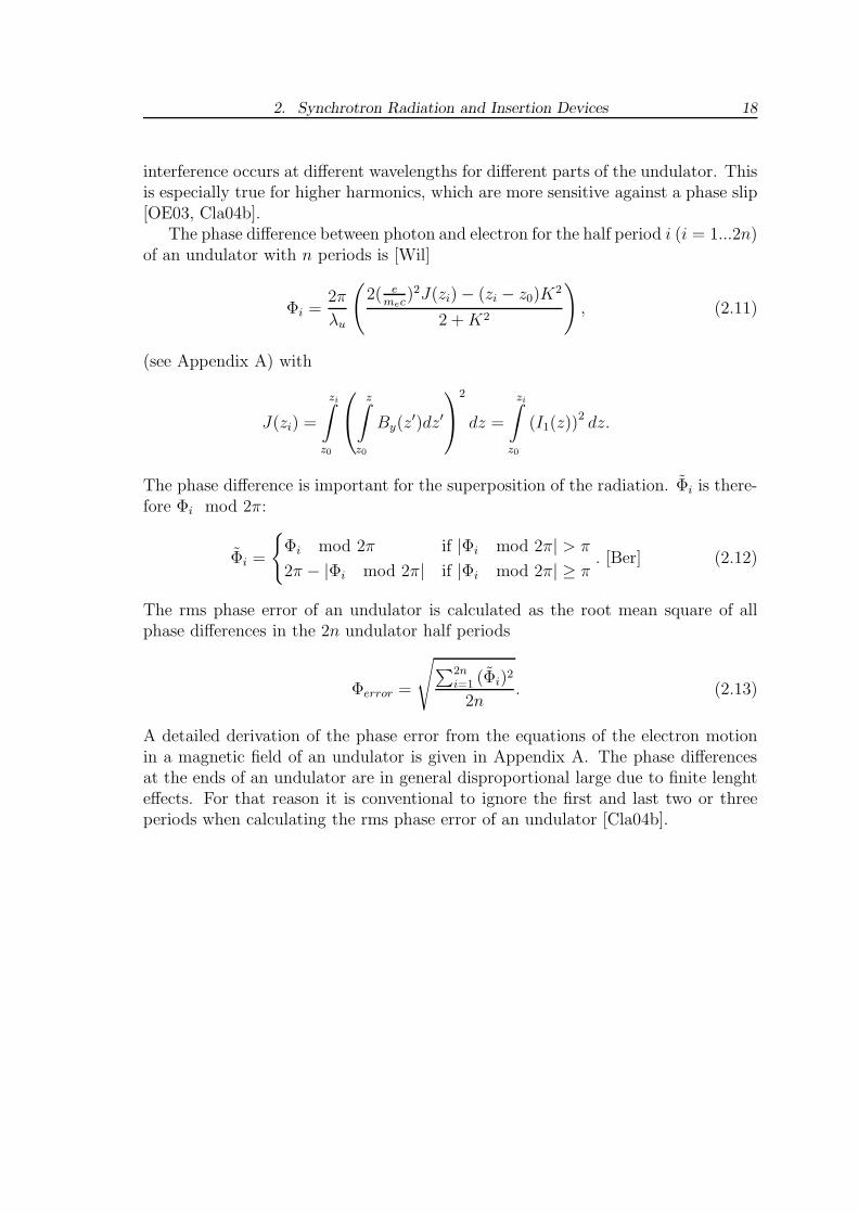
A measure to describe the quality of the magnetic field of an undulator is the so-called phase error.Relativistic electrons emit white light, when deflected. In an undulator, the electronscontinuously emit white light into a narrow cone around the forward direction (z-axis). The maximum deflection angle Θw (see equation (2.9)) of the electrons issmaller than the opening angle of the cone (∼ 1/γ). Therefore the cones overlap andthe photons emitted by a single electron interfere. The interference is constructivewhen the photon is in phase with the electron oscillation. This leads to the previouslydescribed line spectrum (see equation (2.10) and figure 2.9).Disturbances of the uniformity of the magnetic field, like variations in the fieldamplitude B or the period length λu from period to period, cause a change of thelength of the electron trajectory. This yields a phase slip between electron andphoton (see figure 2.12). A phase slip between the electron and the photon causes a
e−
hν
hν
x
z
∆φe = ∆φhν = π∆φe = ∆φhν = π∆φe = ∆φhν = π
Fig. 2.12: Schematical drawing of the required correlation between the electron motion(blue) in the magnetic field of an undulator and the emitted light (green) withone wavelength to achieve constructive interference.
line broadening and intensity reduction of the emitted lines because the constructive
2. Synchrotron Radiation and Insertion Devices 18
interference occurs at different wavelengths for different parts of the undulator. Thisis especially true for higher harmonics, which are more sensitive against a phase slip[OE03, Cla04b].
The phase difference between photon and electron for the half period i (i = 1...2n)of an undulator with n periods is [Wil]
Φi =2π
λu
(
2( emec
)2J(zi) − (zi − z0)K2
2 + K2
)
, (2.11)
(see Appendix A) with
J(zi) =
zi∫
z0
z∫
z0
By(z′)dz′
2
dz =
zi∫
z0
(I1(z))2 dz.
The phase difference is important for the superposition of the radiation. Φi is there-fore Φi mod 2π:
Φi =
{
Φi mod 2π if |Φi mod 2π| > π
2π − |Φi mod 2π| if |Φi mod 2π| ≥ π. [Ber] (2.12)
The rms phase error of an undulator is calculated as the root mean square of allphase differences in the 2n undulator half periods
Φerror =
√
∑2ni=1 (Φi)2
2n. (2.13)
A detailed derivation of the phase error from the equations of the electron motionin a magnetic field of an undulator is given in Appendix A. The phase differencesat the ends of an undulator are in general disproportional large due to finite lenghteffects. For that reason it is conventional to ignore the first and last two or threeperiods when calculating the rms phase error of an undulator [Cla04b].
3. MAGNETIC FIELD ERRORS CAUSED BY FINITEMECHANICAL TOLERANCES
In superconductive undulators field errors are mainly caused by finite mechanicaltolerances. In addition possible error sources are variations in the quality of the polematerial and persistent currents. Both are not considered in this thesis.In a first step the possible mechanical deviations appearing in superconductive coilsare described and their influence on the magnetic field is analyzed. In addition it isshown how deviations in the pole height and the wire bundle position act differentlyon the field and how they can be distinguished from each other.
3.1 Types of mechanical deviations
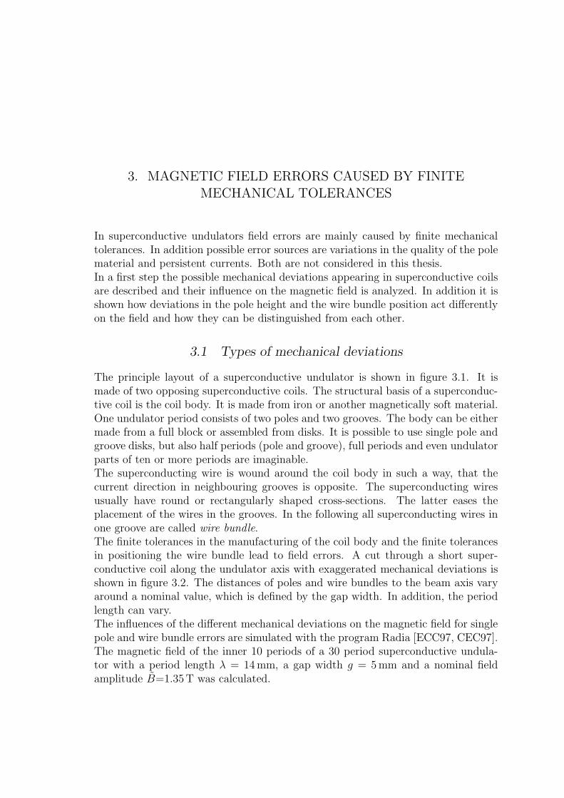
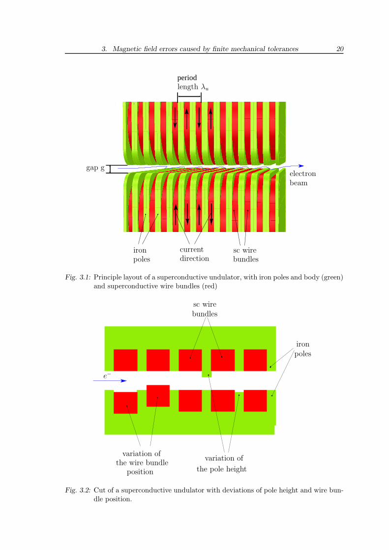
The principle layout of a superconductive undulator is shown in figure 3.1. It ismade of two opposing superconductive coils. The structural basis of a superconduc-tive coil is the coil body. It is made from iron or another magnetically soft material.One undulator period consists of two poles and two grooves. The body can be eithermade from a full block or assembled from disks. It is possible to use single pole andgroove disks, but also half periods (pole and groove), full periods and even undulatorparts of ten or more periods are imaginable.The superconducting wire is wound around the coil body in such a way, that thecurrent direction in neighbouring grooves is opposite. The superconducting wiresusually have round or rectangularly shaped cross-sections. The latter eases theplacement of the wires in the grooves. In the following all superconducting wires inone groove are called wire bundle.The finite tolerances in the manufacturing of the coil body and the finite tolerancesin positioning the wire bundle lead to field errors. A cut through a short super-conductive coil along the undulator axis with exaggerated mechanical deviations isshown in figure 3.2. The distances of poles and wire bundles to the beam axis varyaround a nominal value, which is defined by the gap width. In addition, the periodlength can vary.The influences of the different mechanical deviations on the magnetic field for singlepole and wire bundle errors are simulated with the program Radia [ECC97, CEC97].The magnetic field of the inner 10 periods of a 30 period superconductive undula-tor with a period length λ = 14 mm, a gap width g = 5 mm and a nominal fieldamplitude B=1.35T was calculated.
3. Magnetic field errors caused by finite mechanical tolerances 20
period
ironpoles
currentdirection
sc wirebundles
electronbeam
gap g
length λu
Fig. 3.1: Principle layout of a superconductive undulator, with iron poles and body (green)and superconductive wire bundles (red)
ironpoles
sc wirebundles
e−
variation ofvariation of
the wire bundleposition the pole height
Fig. 3.2: Cut of a superconductive undulator with deviations of pole height and wire bun-dle position.
3. Magnetic field errors caused by finite mechanical tolerances 21
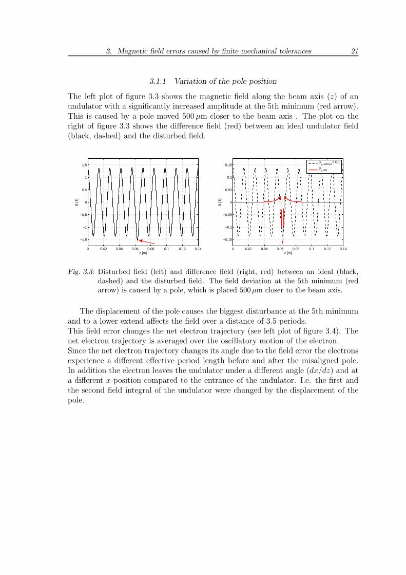
3.1.1 Variation of the pole position
The left plot of figure 3.3 shows the magnetic field along the beam axis (z) of anundulator with a significantly increased amplitude at the 5th minimum (red arrow).This is caused by a pole moved 500 µm closer to the beam axis . The plot on theright of figure 3.3 shows the difference field (red) between an ideal undulator field(black, dashed) and the disturbed field.
0 0.02 0.04 0.06 0.08 0.1 0.12 0.14
−1.5
−1
−0.5
0
0.5
1
1.5
z [m]
B [T
]
0 0.02 0.04 0.06 0.08 0.1 0.12 0.14
−0.15
−0.1
−0.05
0
0.05
0.1
0.15
z [m]
B [T
]
B
y, without × 0.1
By, diff
Fig. 3.3: Disturbed field (left) and difference field (right, red) between an ideal (black,dashed) and the disturbed field. The field deviation at the 5th minimum (redarrow) is caused by a pole, which is placed 500µm closer to the beam axis.
The displacement of the pole causes the biggest disturbance at the 5th minimumand to a lower extend affects the field over a distance of 3.5 periods.This field error changes the net electron trajectory (see left plot of figure 3.4). Thenet electron trajectory is averaged over the oscillatory motion of the electron.Since the net electron trajectory changes its angle due to the field error the electronsexperience a different effective period length before and after the misaligned pole.In addition the electron leaves the undulator under a different angle (dx/dz) and ata different x-position compared to the entrance of the undulator. I.e. the first andthe second field integral of the undulator were changed by the displacement of thepole.
3. Magnetic field errors caused by finite mechanical tolerances 22
0 0.02 0.04 0.06 0.08 0.1 0.12 0.14−4
−3
−2
−1
0
1
2x 10
−7
z [m]
x [m
]
electron trajectory
0 0.02 0.04 0.06 0.08 0.1 0.12 0.14−1
0
1
2
3
4
5
z [m]
Pha
se d
iffer
ence
[deg
ree]
Fig. 3.4: Disturbance of the electron trajectory (left) and phase difference between electronand photon (right). Both are caused by the pole at the 5th minimum, which ismoved 500µm closer to the beam axis. The electron beam energy is 2.5GeV.
The phase difference between electron and photon is shown in the right plotof figure 3.4. After passing the area with the disturbed field the phase differenceincreases linearly with z. Therefore, the undulator is divided into two parts andeach part is radiating with a different wave-length.
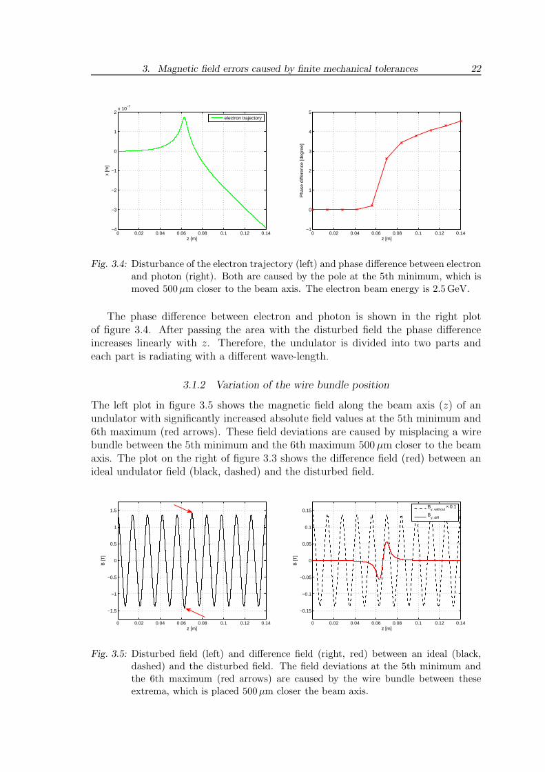
3.1.2 Variation of the wire bundle position
The left plot in figure 3.5 shows the magnetic field along the beam axis (z) of anundulator with significantly increased absolute field values at the 5th minimum and6th maximum (red arrows). These field deviations are caused by misplacing a wirebundle between the 5th minimum and the 6th maximum 500 µm closer to the beamaxis. The plot on the right of figure 3.3 shows the difference field (red) between anideal undulator field (black, dashed) and the disturbed field.
0 0.02 0.04 0.06 0.08 0.1 0.12 0.14
−1.5
−1
−0.5
0
0.5
1
1.5
z [m]
B [T
]
0 0.02 0.04 0.06 0.08 0.1 0.12 0.14
−0.15
−0.1
−0.05
0
0.05
0.1
0.15
z [m]
B [T
]
B
y, without × 0.1
By, diff
Fig. 3.5: Disturbed field (left) and difference field (right, red) between an ideal (black,dashed) and the disturbed field. The field deviations at the 5th minimum andthe 6th maximum (red arrows) are caused by the wire bundle between theseextrema, which is placed 500µm closer the beam axis.
3. Magnetic field errors caused by finite mechanical tolerances 23
0 0.02 0.04 0.06 0.08 0.1 0.12 0.14−8
−7
−6
−5
−4
−3
−2
−1
0x 10
−7
z [m]
x [m
]
electron trajectory
0 0.02 0.04 0.06 0.08 0.1 0.12 0.14−2
0
2
4
6
8
10
12
14
z [m]
Pha
se d
iffer
ence
[deg
ree]
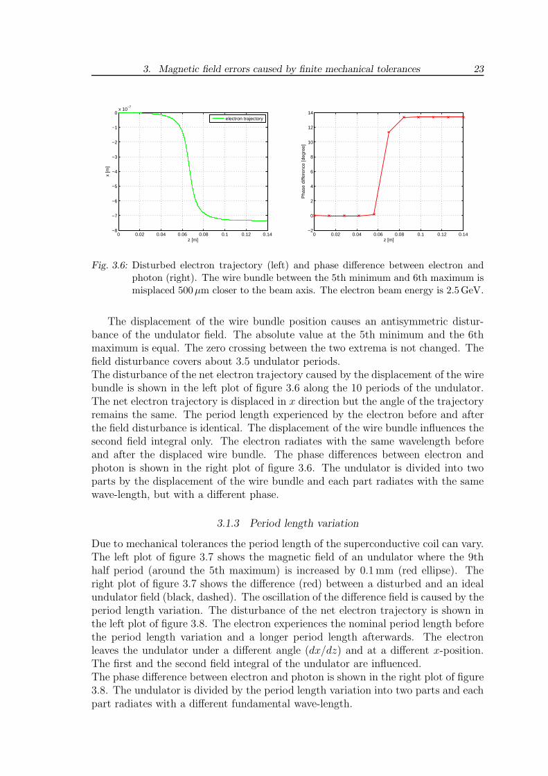
Fig. 3.6: Disturbed electron trajectory (left) and phase difference between electron andphoton (right). The wire bundle between the 5th minimum and 6th maximum ismisplaced 500µm closer to the beam axis. The electron beam energy is 2.5GeV.
The displacement of the wire bundle position causes an antisymmetric distur-bance of the undulator field. The absolute value at the 5th minimum and the 6thmaximum is equal. The zero crossing between the two extrema is not changed. Thefield disturbance covers about 3.5 undulator periods.The disturbance of the net electron trajectory caused by the displacement of the wirebundle is shown in the left plot of figure 3.6 along the 10 periods of the undulator.The net electron trajectory is displaced in x direction but the angle of the trajectoryremains the same. The period length experienced by the electron before and afterthe field disturbance is identical. The displacement of the wire bundle influences thesecond field integral only. The electron radiates with the same wavelength beforeand after the displaced wire bundle. The phase differences between electron andphoton is shown in the right plot of figure 3.6. The undulator is divided into twoparts by the displacement of the wire bundle and each part radiates with the samewave-length, but with a different phase.
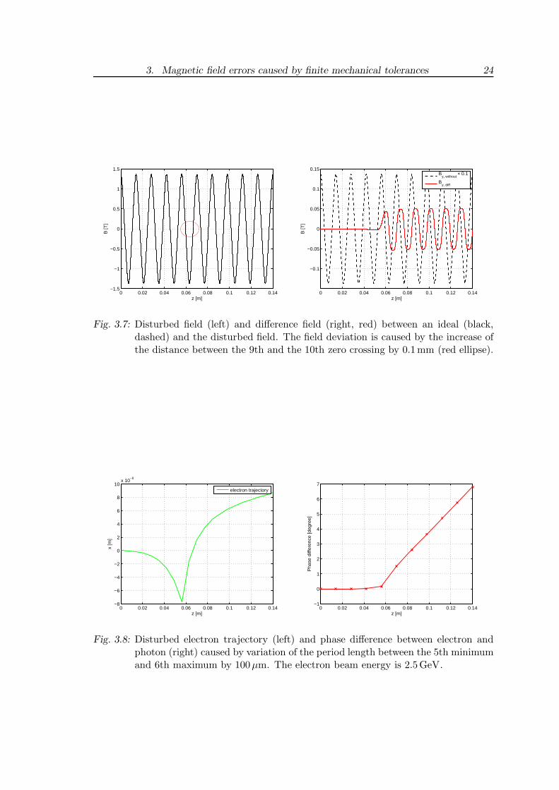
3.1.3 Period length variation
Due to mechanical tolerances the period length of the superconductive coil can vary.The left plot of figure 3.7 shows the magnetic field of an undulator where the 9thhalf period (around the 5th maximum) is increased by 0.1 mm (red ellipse). Theright plot of figure 3.7 shows the difference (red) between a disturbed and an idealundulator field (black, dashed). The oscillation of the difference field is caused by theperiod length variation. The disturbance of the net electron trajectory is shown inthe left plot of figure 3.8. The electron experiences the nominal period length beforethe period length variation and a longer period length afterwards. The electronleaves the undulator under a different angle (dx/dz) and at a different x-position.The first and the second field integral of the undulator are influenced.The phase difference between electron and photon is shown in the right plot of figure3.8. The undulator is divided by the period length variation into two parts and eachpart radiates with a different fundamental wave-length.
3. Magnetic field errors caused by finite mechanical tolerances 24
0 0.02 0.04 0.06 0.08 0.1 0.12 0.14−1.5
−1
−0.5
0
0.5
1
1.5
z [m]
B [T
]
0 0.02 0.04 0.06 0.08 0.1 0.12 0.14
−0.1
−0.05
0
0.05
0.1
0.15
z [m]B
[T]
B
y, without × 0.1
By, diff
Fig. 3.7: Disturbed field (left) and difference field (right, red) between an ideal (black,dashed) and the disturbed field. The field deviation is caused by the increase ofthe distance between the 9th and the 10th zero crossing by 0.1mm (red ellipse).
0 0.02 0.04 0.06 0.08 0.1 0.12 0.14−8
−6
−4
−2
0
2
4
6
8
10x 10
−8
z [m]
x [m
]
electron trajectory
0 0.02 0.04 0.06 0.08 0.1 0.12 0.14−1
0
1
2
3
4
5
6
7
z [m]
Pha
se d
iffer
ence
[deg
ree]
Fig. 3.8: Disturbed electron trajectory (left) and phase difference between electron andphoton (right) caused by variation of the period length between the 5th minimumand 6th maximum by 100µm. The electron beam energy is 2.5GeV.
3. Magnetic field errors caused by finite mechanical tolerances 25
0 200 400 600 800 10000
0.2
0.4
0.6
0.8
1
1.2
1.4
current density [A/mm2]
By,
max
[T]
without
pole deviation: 250 µm
wire bundle deviation: 250 µm
Fig. 3.9: Amplitude of the magnetic flux density versus current density for an ideal undu-lator (red), an undulator with a deviation of the pole position against the beamaxis by 250µm (blue) and an undulator with a deviation of the wire bundleposition against the beam axis by 250µm (green).
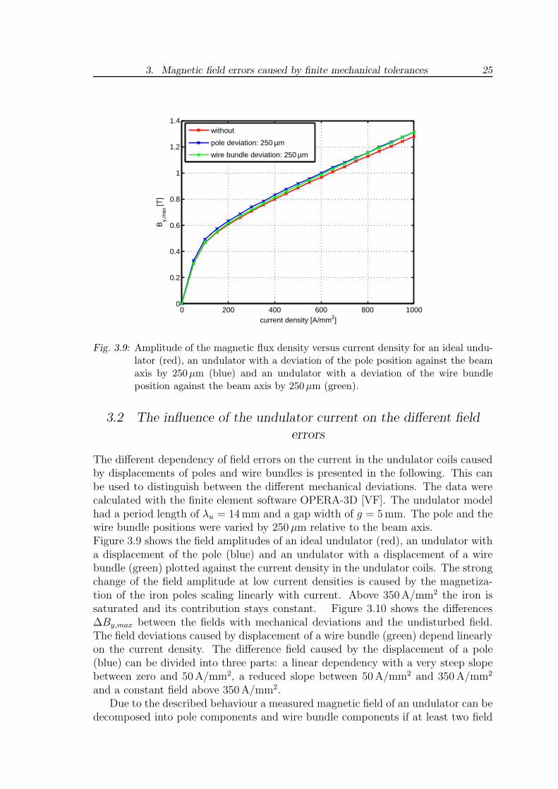
3.2 The influence of the undulator current on the different fielderrors
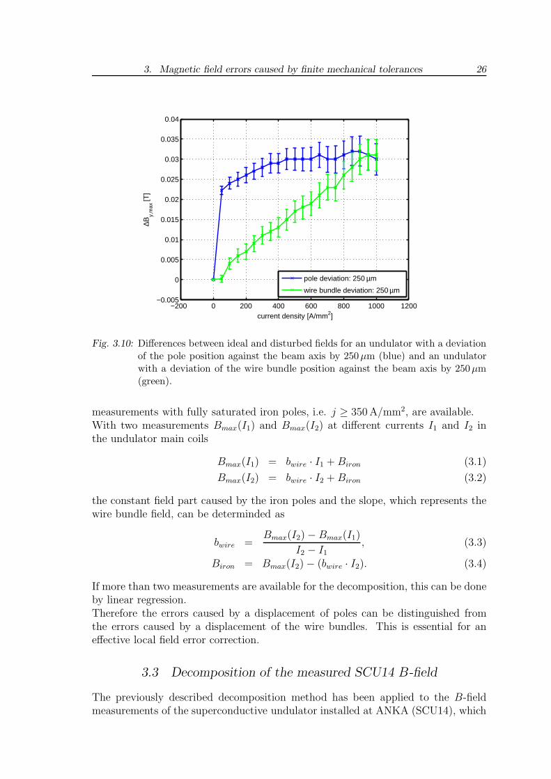
The different dependency of field errors on the current in the undulator coils causedby displacements of poles and wire bundles is presented in the following. This canbe used to distinguish between the different mechanical deviations. The data werecalculated with the finite element software OPERA-3D [VF]. The undulator modelhad a period length of λu = 14 mm and a gap width of g = 5 mm. The pole and thewire bundle positions were varied by 250 µm relative to the beam axis.Figure 3.9 shows the field amplitudes of an ideal undulator (red), an undulator witha displacement of the pole (blue) and an undulator with a displacement of a wirebundle (green) plotted against the current density in the undulator coils. The strongchange of the field amplitude at low current densities is caused by the magnetiza-tion of the iron poles scaling linearly with current. Above 350 A/mm2 the iron issaturated and its contribution stays constant. Figure 3.10 shows the differences∆By,max between the fields with mechanical deviations and the undisturbed field.The field deviations caused by displacement of a wire bundle (green) depend linearlyon the current density. The difference field caused by the displacement of a pole(blue) can be divided into three parts: a linear dependency with a very steep slopebetween zero and 50 A/mm2, a reduced slope between 50 A/mm2 and 350 A/mm2
and a constant field above 350 A/mm2.Due to the described behaviour a measured magnetic field of an undulator can be
decomposed into pole components and wire bundle components if at least two field
3. Magnetic field errors caused by finite mechanical tolerances 26
−200 0 200 400 600 800 1000 1200−0.005
0
0.005
0.01
0.015
0.02
0.025
0.03
0.035
0.04
current density [A/mm2]
∆By,
max
[T]
pole deviation: 250 µm
wire bundle deviation: 250 µm
Fig. 3.10: Differences between ideal and disturbed fields for an undulator with a deviationof the pole position against the beam axis by 250µm (blue) and an undulatorwith a deviation of the wire bundle position against the beam axis by 250µm(green).
measurements with fully saturated iron poles, i.e. j ≥ 350 A/mm2, are available.With two measurements Bmax(I1) and Bmax(I2) at different currents I1 and I2 inthe undulator main coils
Bmax(I1) = bwire · I1 + Biron (3.1)
Bmax(I2) = bwire · I2 + Biron (3.2)
the constant field part caused by the iron poles and the slope, which represents thewire bundle field, can be determinded as
bwire =Bmax(I2) − Bmax(I1)
I2 − I1, (3.3)
Biron = Bmax(I2) − (bwire · I2). (3.4)
If more than two measurements are available for the decomposition, this can be doneby linear regression.Therefore the errors caused by a displacement of poles can be distinguished fromthe errors caused by a displacement of the wire bundles. This is essential for aneffective local field error correction.
3.3 Decomposition of the measured SCU14 B-field
The previously described decomposition method has been applied to the B-fieldmeasurements of the superconductive undulator installed at ANKA (SCU14), which

3. Magnetic field errors caused by finite mechanical tolerances 27
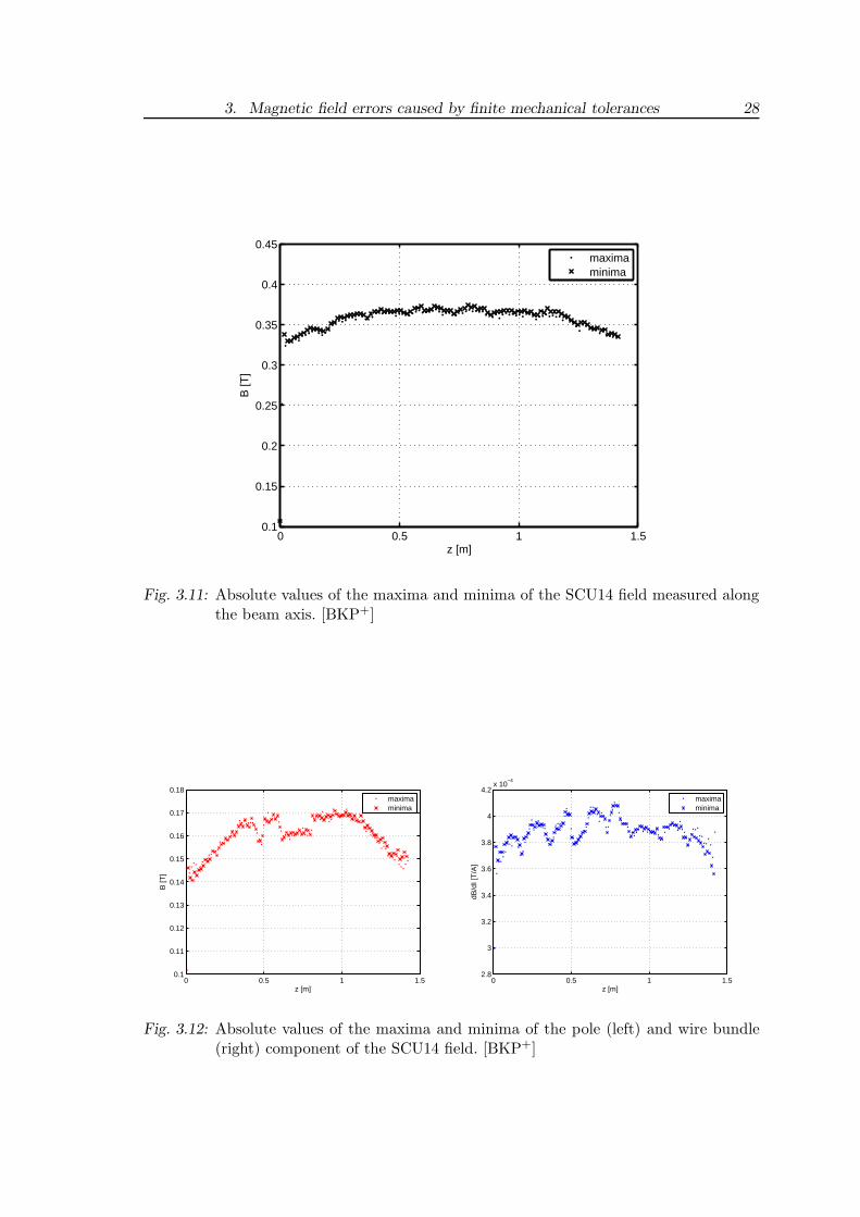
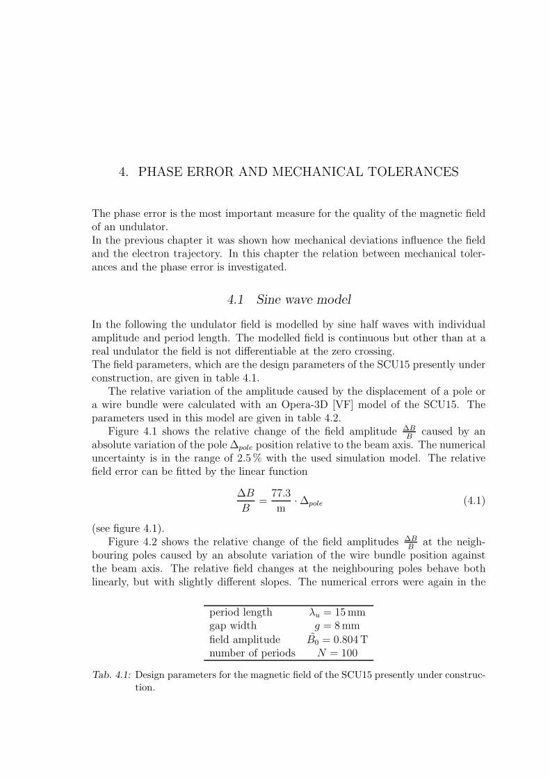
were performed by Accel Instruments GmbH, Bergisch Gladbach, Germany, beforemounting the coils into the cryostat.Figure 3.11 shows field amplitudes along the beam axis (z-axis) at a current densityof 500 A/mm2. The measurement shows that the field at the ends of the undulatoris lower and that the field strength oscillates with a period length of 12.5 undulatorperiods.From a previous detailed analyses it is know, that the first is caused by a bendingof the coils - i.e. wire bundles and poles - while the vacuum vessel surrounding thecoils was welded. The end of each coil is about 250 µm further away from the beamthan the center. The second field deviation was caused by a mechanically unevenstamp with a length of 12.5 undulator periods which pressed the wire bundles intothe grooves of the coil body [Wol05, WBC+06, BKP+].Figure 3.12 shows the decomposition of the SCU14 field into its pole (left) and coil(right) components. It can be clearly seen, that both field components show thebending of the coils. This proves, that the coils are bent as a whole. The oscillationcan be clearly identified in the wire bundle component, but cannot be found in thepole component of the field. Thus, the oscillations in the measured field are causedby mechanical displacements of the wire bundles but not by displacements of thepoles.Besides the bending the analysis shows two additional major mechanical deviationsin the position of the poles against the beam axis.
3. Magnetic field errors caused by finite mechanical tolerances 28
0 0.5 1 1.50.1
0.15
0.2
0.25
0.3
0.35
0.4
0.45
z [m]
B [T
]
maximaminima
Fig. 3.11: Absolute values of the maxima and minima of the SCU14 field measured alongthe beam axis. [BKP+]
0 0.5 1 1.50.1
0.11
0.12
0.13
0.14
0.15
0.16
0.17
0.18
z [m]
B [T
]
maximaminima
0 0.5 1 1.52.8
3
3.2
3.4
3.6
3.8
4
4.2x 10
−4
z [m]
dB/d
I [T
/A]
maximaminima
Fig. 3.12: Absolute values of the maxima and minima of the pole (left) and wire bundle(right) component of the SCU14 field. [BKP+]
4. PHASE ERROR AND MECHANICAL TOLERANCES
The phase error is the most important measure for the quality of the magnetic fieldof an undulator.In the previous chapter it was shown how mechanical deviations influence the fieldand the electron trajectory. In this chapter the relation between mechanical toler-ances and the phase error is investigated.
4.1 Sine wave model
In the following the undulator field is modelled by sine half waves with individualamplitude and period length. The modelled field is continuous but other than at areal undulator the field is not differentiable at the zero crossing.The field parameters, which are the design parameters of the SCU15 presently underconstruction, are given in table 4.1.
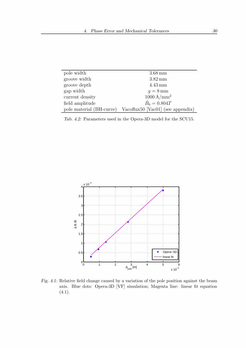
The relative variation of the amplitude caused by the displacement of a pole ora wire bundle were calculated with an Opera-3D [VF] model of the SCU15. Theparameters used in this model are given in table 4.2.
Figure 4.1 shows the relative change of the field amplitude ∆BB
caused by anabsolute variation of the pole ∆pole position relative to the beam axis. The numericaluncertainty is in the range of 2.5 % with the used simulation model. The relativefield error can be fitted by the linear function
∆B
B=
77.3
m· ∆pole (4.1)
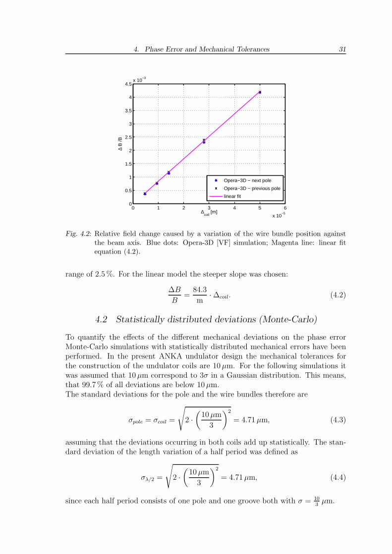
(see figure 4.1).Figure 4.2 shows the relative change of the field amplitudes ∆B
Bat the neigh-
bouring poles caused by an absolute variation of the wire bundle position againstthe beam axis. The relative field changes at the neighbouring poles behave bothlinearly, but with slightly different slopes. The numerical errors were again in the
period length λu = 15 mmgap width g = 8 mm
field amplitude B0 = 0.804 Tnumber of periods N = 100
Tab. 4.1: Design parameters for the magnetic field of the SCU15 presently under construc-tion.
4. Phase Error and Mechanical Tolerances 30
pole width 3.68 mmgroove width 3.82 mmgroove depth 4.43 mmgap width g = 8 mmcurrent density 1000 A/mm2
field amplitude B0 = 0.804Tpole material (BH-curve) Vacoflux50 [Vac01] (see appendix)
Tab. 4.2: Parameters used in the Opera-3D model for the SCU15.
0 1 2 3 4 5 6
x 10−5
0
0.5
1
1.5
2
2.5
3
3.5
4x 10
−3
∆pole
[m]
∆ B
/B
Opera−3D
linear fit
Fig. 4.1: Relative field change caused by a variation of the pole position against the beamaxis. Blue dots: Opera-3D [VF] simulation; Magenta line: linear fit equation(4.1).
4. Phase Error and Mechanical Tolerances 31
0 1 2 3 4 5 6
x 10−5
0
0.5
1
1.5
2
2.5
3
3.5
4
4.5x 10
−3
∆coil
[m]
∆ B
/B
Opera−3D − next pole
Opera−3D − previous pole
linear fit
Fig. 4.2: Relative field change caused by a variation of the wire bundle position againstthe beam axis. Blue dots: Opera-3D [VF] simulation; Magenta line: linear fitequation (4.2).
range of 2.5 %. For the linear model the steeper slope was chosen:
∆B
B=
84.3
m· ∆coil. (4.2)
4.2 Statistically distributed deviations (Monte-Carlo)
To quantify the effects of the different mechanical deviations on the phase errorMonte-Carlo simulations with statistically distributed mechanical errors have beenperformed. In the present ANKA undulator design the mechanical tolerances forthe construction of the undulator coils are 10 µm. For the following simulations itwas assumed that 10 µm correspond to 3σ in a Gaussian distribution. This means,that 99.7 % of all deviations are below 10 µm.The standard deviations for the pole and the wire bundles therefore are
σpole = σcoil =
√
2 ·
(
10 µm
3
)2
= 4.71 µm, (4.3)
assuming that the deviations occurring in both coils add up statistically. The stan-dard deviation of the length variation of a half period was defined as
σλ/2 =
√
2 ·
(
10 µm
3
)2
= 4.71 µm, (4.4)
since each half period consists of one pole and one groove both with σ = 103
µm.
4. Phase Error and Mechanical Tolerances 32
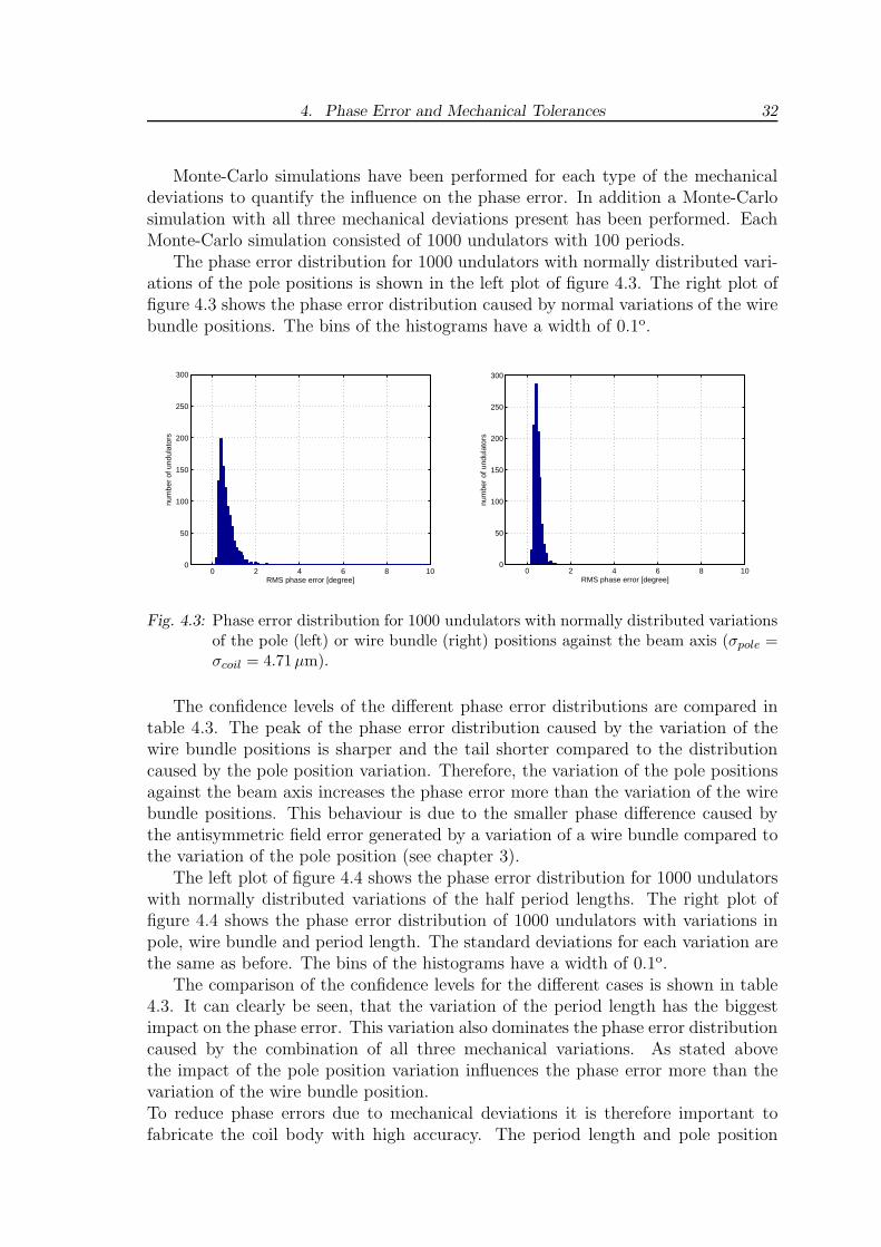
Monte-Carlo simulations have been performed for each type of the mechanicaldeviations to quantify the influence on the phase error. In addition a Monte-Carlosimulation with all three mechanical deviations present has been performed. EachMonte-Carlo simulation consisted of 1000 undulators with 100 periods.
The phase error distribution for 1000 undulators with normally distributed vari-ations of the pole positions is shown in the left plot of figure 4.3. The right plot offigure 4.3 shows the phase error distribution caused by normal variations of the wirebundle positions. The bins of the histograms have a width of 0.1o.
0 2 4 6 8 100
50
100
150
200
250
300
RMS phase error [degree]
num
ber
of u
ndul
ator
s
0 2 4 6 8 100
50
100
150
200
250
300
RMS phase error [degree]
num
ber
of u
ndul
ator
s
Fig. 4.3: Phase error distribution for 1000 undulators with normally distributed variationsof the pole (left) or wire bundle (right) positions against the beam axis (σpole =σcoil = 4.71µm).
The confidence levels of the different phase error distributions are compared intable 4.3. The peak of the phase error distribution caused by the variation of thewire bundle positions is sharper and the tail shorter compared to the distributioncaused by the pole position variation. Therefore, the variation of the pole positionsagainst the beam axis increases the phase error more than the variation of the wirebundle positions. This behaviour is due to the smaller phase difference caused bythe antisymmetric field error generated by a variation of a wire bundle compared tothe variation of the pole position (see chapter 3).
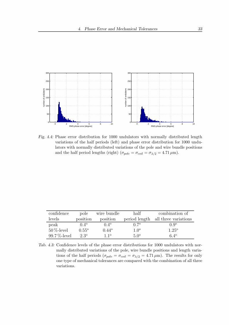
The left plot of figure 4.4 shows the phase error distribution for 1000 undulatorswith normally distributed variations of the half period lengths. The right plot offigure 4.4 shows the phase error distribution of 1000 undulators with variations inpole, wire bundle and period length. The standard deviations for each variation arethe same as before. The bins of the histograms have a width of 0.1o.
The comparison of the confidence levels for the different cases is shown in table4.3. It can clearly be seen, that the variation of the period length has the biggestimpact on the phase error. This variation also dominates the phase error distributioncaused by the combination of all three mechanical variations. As stated abovethe impact of the pole position variation influences the phase error more than thevariation of the wire bundle position.To reduce phase errors due to mechanical deviations it is therefore important tofabricate the coil body with high accuracy. The period length and pole position
4. Phase Error and Mechanical Tolerances 33
0 2 4 6 8 100
50
100
150
200
250
300
RMS phase error [degree]
num
ber
of u
ndul
ator
s
0 2 4 6 8 100
50
100
150
200
250
300
RMS phase error [degree]nu
mbe
r of
und
ulat
ors
Fig. 4.4: Phase error distribution for 1000 undulators with normally distributed lengthvariations of the half periods (left) and phase error distribution for 1000 undu-lators with normally distributed variations of the pole and wire bundle positionsand the half period lengths (right) (σpole = σcoil = σλ/2 = 4.71µm).
confidence pole wire bundle half combination oflevels position position period length all three variationspeak 0.4o 0.4o 0.7o 0.9o
50 %-level 0.55o 0.44o 1.0o 1.25o
99.7 %-level 2.3o 1.1o 5.0o 6.4o
Tab. 4.3: Confidence levels of the phase error distributions for 1000 undulators with nor-mally distributed variations of the pole, wire bundle positions and length varia-tions of the half periods (σpole = σcoil = σλ/2 = 4.71µm). The results for onlyone type of mechanical tolerances are compared with the combination of all threevariations.
4. Phase Error and Mechanical Tolerances 34
���������������������������������������������������
���������������������������������������������������
Fig. 4.5: Sketch of a linear (left) and a sawtooth deformation (right) of thepoles. [PWBF08]
������������������������������������������������������������������������������������������������������������������
������������������������������������������������������������������������������������������������������������������
Fig. 4.6: Sketch of two possible parabolic deformations of the pole positions - concave(left) and convex (right). [PWBF08]
variations of the body have to be measured and corrected if necessary before winding.
4.3 Systematic variations
The magnetic field of the SCU14 installed at ANKA suffers from systematic errors(see figure 3.11). As discussed in chapter 3.3 these are caused by the bending ofboth coils and by a sinusoidal displacement of the wire bundles.
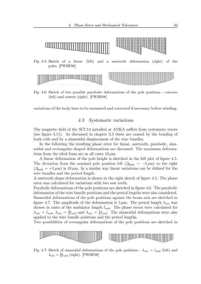
In the following the resulting phase error for linear, sawtooth, parabolic, sinu-soidal and rectangular shaped deformations are discussed. The maximum deforma-tions from the ideal form are in all cases 10 µm.
A linear deformation of the pole height is sketched in the left plot of figure 4.5.The deviation from the nominal pole position left (∆pole = −5 µm) to the right(∆pole = +5 µm) is 10 µm. In a similar way linear variations can be defined for thewire bundles and the period length.A sawtooth shape deformation is shown in the right sketch of figure 4.5. The phaseerror was calculated for variations with two saw teeth.Parabolic deformations of the pole positions are sketched in figure 4.6. The parabolicdeformation of the wire bundle positions and the period lengths were also considered.Sinusoidal deformations of the pole positions against the beam axis are sketched infigure 4.7. The amplitude of the deformation is 5 µm. The period length λsin waschosen in units of the undulator length lund. The phase errors were calculated forλsin = lund, λsin = 2
3lund and λsin = 1
2lund. The sinusoidal deformations were also
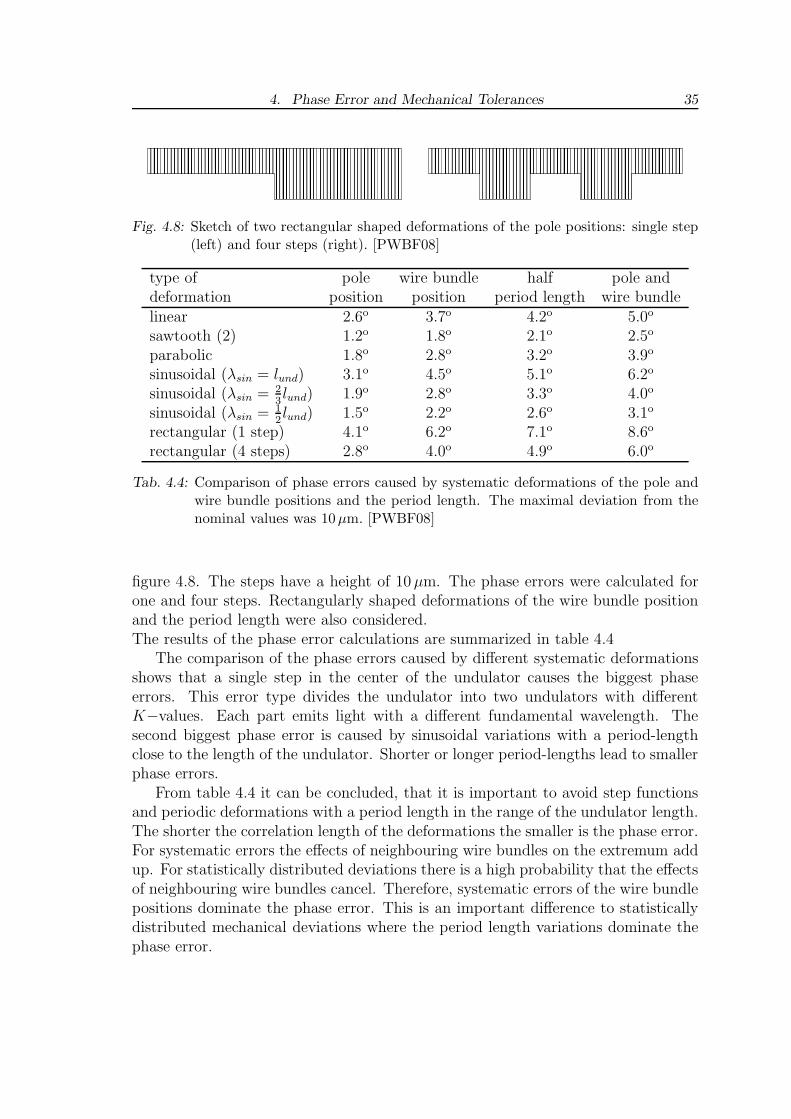
applied to the wire bundle positions and the period lengths.Two possibilities of rectangular deformations of the pole positions are sketched in
����������������������������������������������������������������������������������������������������������������������������
���������������������������������������������������������������������������������������������
��������������������������������������������������������������������������������������������� ����������������������������������������������
��������������������������������������������������������������������������������������������
������������������������������������������������������������������������������������������������������������������������������������������
������������������������������������������������������������������������������������������������������������������������������������������
������������������������������������������������������������������������������������������������������������������������������������������
Fig. 4.7: Sketch of sinusoidal deformations of the pole positions - λsin = lund (left) andλsin = 2
3 lund (right). [PWBF08]
4. Phase Error and Mechanical Tolerances 35
������������������������������������������������������������������������������������������������������������������������������������������������������������
������������������������������������������������������������������������������������������������������������������������������������������������������������
������������������������������������������������������������������������������������������������������������������������������������������������������������
������������������������������������������������������������������������������������������������������������������������������������������������������������
Fig. 4.8: Sketch of two rectangular shaped deformations of the pole positions: single step(left) and four steps (right). [PWBF08]
type of pole wire bundle half pole anddeformation position position period length wire bundlelinear 2.6o 3.7o 4.2o 5.0o
sawtooth (2) 1.2o 1.8o 2.1o 2.5o
parabolic 1.8o 2.8o 3.2o 3.9o
sinusoidal (λsin = lund) 3.1o 4.5o 5.1o 6.2o
sinusoidal (λsin = 23lund) 1.9o 2.8o 3.3o 4.0o
sinusoidal (λsin = 12lund) 1.5o 2.2o 2.6o 3.1o
rectangular (1 step) 4.1o 6.2o 7.1o 8.6o
rectangular (4 steps) 2.8o 4.0o 4.9o 6.0o
Tab. 4.4: Comparison of phase errors caused by systematic deformations of the pole andwire bundle positions and the period length. The maximal deviation from thenominal values was 10µm. [PWBF08]
figure 4.8. The steps have a height of 10 µm. The phase errors were calculated forone and four steps. Rectangularly shaped deformations of the wire bundle positionand the period length were also considered.The results of the phase error calculations are summarized in table 4.4
The comparison of the phase errors caused by different systematic deformationsshows that a single step in the center of the undulator causes the biggest phaseerrors. This error type divides the undulator into two undulators with differentK−values. Each part emits light with a different fundamental wavelength. Thesecond biggest phase error is caused by sinusoidal variations with a period-lengthclose to the length of the undulator. Shorter or longer period-lengths lead to smallerphase errors.
From table 4.4 it can be concluded, that it is important to avoid step functionsand periodic deformations with a period length in the range of the undulator length.The shorter the correlation length of the deformations the smaller is the phase error.For systematic errors the effects of neighbouring wire bundles on the extremum addup. For statistically distributed deviations there is a high probability that the effectsof neighbouring wire bundles cancel. Therefore, systematic errors of the wire bundlepositions dominate the phase error. This is an important difference to statisticallydistributed mechanical deviations where the period length variations dominate thephase error.
5. CLASSICAL SHIMMING METHODS FORSUPERCONDUCTIVE UNDULATORS
The field quality is a major issue for using superconductive undulators in current3rd and future 4th generation synchrotron light sources, like Free electron Lasers(FEL) or Energy Recovering Linacs (ERL). To obtain phase errors of ≈ 1o thefield errors have to be corrected or shimmed. The up to now known shimmingmethods for superconductive undulators are: mechanical shimming, shimming withintegral correctors and active shimming with separately powered local correctioncoils. Correction coils in superconductive undulators have to be also superconduc-tive. Otherwise they would warm up the cold mass of the undulator. Therefore inthe following all active correction coils for superconductive undulators are consid-ered to be superconductive wires or loops.In the following the different classical shimming methods are presented. Their ad-vantages, disadvantages and limitations are discussed.
5.1 Mechanical shimming methods
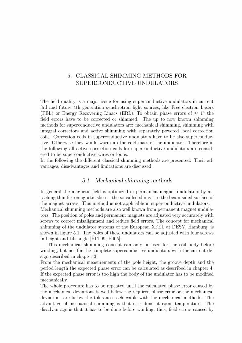
In general the magnetic field is optimized in permanent magnet undulators by at-taching thin ferromagnetic slices - the so-called shims - to the beam-sided surface ofthe magnet arrays. This method is not applicable in superconductive undulators.Mechanical shimming methods are also well known from permanent magnet undula-tors. The position of poles and permanent magnets are adjusted very accurately withscrews to correct misalignment and reduce field errors. The concept for mechanicalshimming of the undulator systems of the European XFEL at DESY, Hamburg, isshown in figure 5.1. The poles of these undulators can be adjusted with four screwsin height and tilt angle [PLT99, Pfl05].
This mechanical shimming concept can only be used for the coil body beforewinding, but not for the complete superconductive undulators with the current de-sign described in chapter 3.From the mechanical measurements of the pole height, the groove depth and theperiod length the expected phase error can be calculated as described in chapter 4.If the expected phase error is too high the body of the undulator has to be modifiedmechanically.The whole procedure has to be repeated until the calculated phase error caused bythe mechanical deviations is well below the required phase error or the mechanicaldeviations are below the tolerances achievable with the mechanical methods. Theadvantage of mechanical shimming is that it is done at room temperature. Thedisadvantage is that it has to be done before winding, thus, field errors caused by
5. Classical shimming methods for superconductive undulators 37
Fig. 5.1: The cross section of a permanent magnet undulator shows the mechanical shim-ming concept for the undulator systems of the European XFEL at DESY, Ham-burg. The pole (grey-blue) of the undulator can be adjusted with four screws(dark-gray-blue) in height (±0.3mm) and tilt angle (±0.1mrad) [PLT99, Pfl05].
misplacements of wire bundles cannot be corrected with this method.
5.2 Shimming with integral correctors
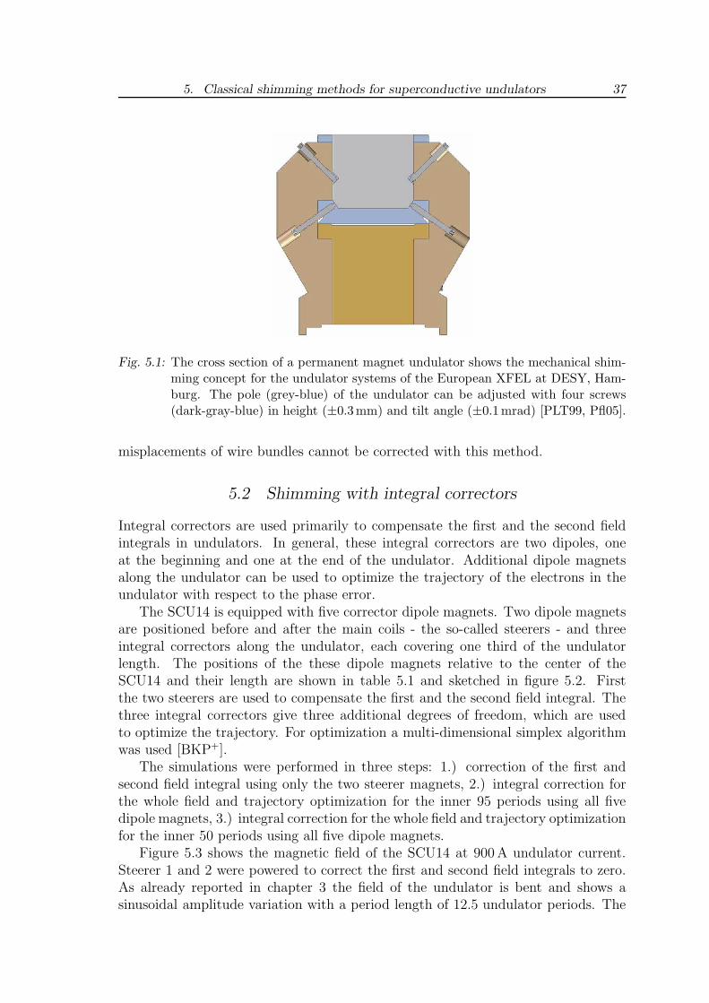
Integral correctors are used primarily to compensate the first and the second fieldintegrals in undulators. In general, these integral correctors are two dipoles, oneat the beginning and one at the end of the undulator. Additional dipole magnetsalong the undulator can be used to optimize the trajectory of the electrons in theundulator with respect to the phase error.
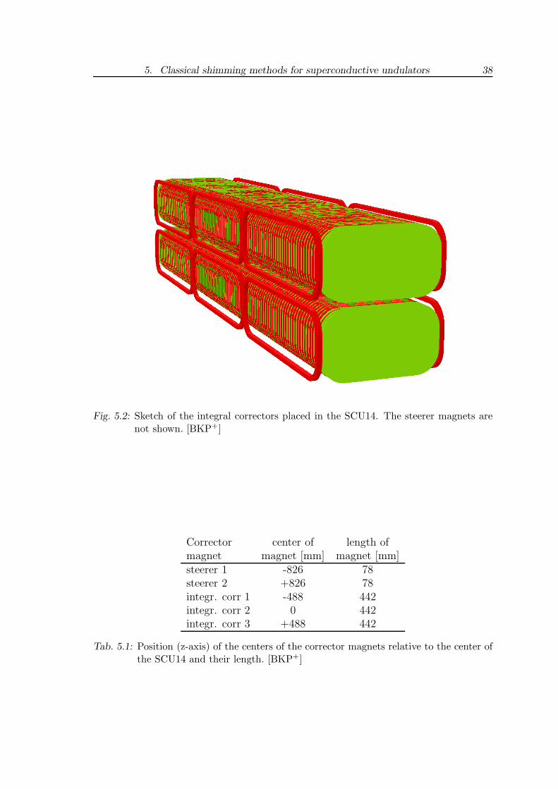
The SCU14 is equipped with five corrector dipole magnets. Two dipole magnetsare positioned before and after the main coils - the so-called steerers - and threeintegral correctors along the undulator, each covering one third of the undulatorlength. The positions of the these dipole magnets relative to the center of theSCU14 and their length are shown in table 5.1 and sketched in figure 5.2. Firstthe two steerers are used to compensate the first and the second field integral. Thethree integral correctors give three additional degrees of freedom, which are usedto optimize the trajectory. For optimization a multi-dimensional simplex algorithmwas used [BKP+].
The simulations were performed in three steps: 1.) correction of the first andsecond field integral using only the two steerer magnets, 2.) integral correction forthe whole field and trajectory optimization for the inner 95 periods using all fivedipole magnets, 3.) integral correction for the whole field and trajectory optimizationfor the inner 50 periods using all five dipole magnets.
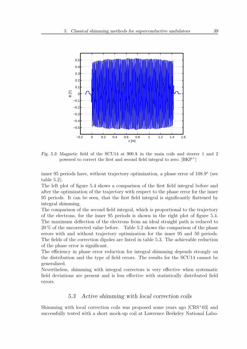
Figure 5.3 shows the magnetic field of the SCU14 at 900 A undulator current.Steerer 1 and 2 were powered to correct the first and second field integrals to zero.As already reported in chapter 3 the field of the undulator is bent and shows asinusoidal amplitude variation with a period length of 12.5 undulator periods. The
5. Classical shimming methods for superconductive undulators 38
Fig. 5.2: Sketch of the integral correctors placed in the SCU14. The steerer magnets arenot shown. [BKP+]
Corrector center of length ofmagnet magnet [mm] magnet [mm]steerer 1 -826 78steerer 2 +826 78integr. corr 1 -488 442integr. corr 2 0 442integr. corr 3 +488 442
Tab. 5.1: Position (z-axis) of the centers of the corrector magnets relative to the center ofthe SCU14 and their length. [BKP+]
5. Classical shimming methods for superconductive undulators 39
−0.2 0 0.2 0.4 0.6 0.8 1 1.2 1.4 1.6
−0.5
−0.4
−0.3
−0.2
−0.1
0
0.1
0.2
0.3
0.4
0.5
z [m]
B [T
]
Fig. 5.3: Magnetic field of the SCU14 at 900A in the main coils and steerer 1 and 2powered to correct the first and second field integral to zero. [BKP+]
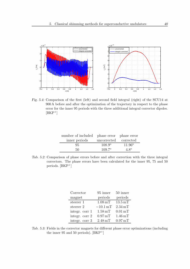
inner 95 periods have, without trajectory optimization, a phase error of 108.9o (seetable 5.2).The left plot of figure 5.4 shows a comparison of the first field integral before andafter the optimization of the trajectory with respect to the phase error for the inner95 periods. It can be seen, that the first field integral is significantly flattened byintegral shimming.The comparison of the second field integral, which is proportional to the trajectoryof the electrons, for the inner 95 periods is shown in the right plot of figure 5.4.The maximum deflection of the electrons from an ideal straight path is reduced to20 % of the uncorrected value before. Table 5.2 shows the comparison of the phaseerrors with and without trajectory optimization for the inner 95 and 50 periods.The fields of the correction dipoles are listed in table 5.3. The achievable reductionof the phase error is significant.The efficiency in phase error reduction for integral shimming depends strongly onthe distribution and the type of field errors. The results for the SCU14 cannot begeneralized.Nevertheless, shimming with integral correctors is very effective when systematicfield deviations are present and is less effective with statistically distributed fielderrors.
5.3 Active shimming with local correction coils
Shimming with local correction coils was proposed some years ago [CRS+03] andsuccessfully tested with a short mock-up coil at Lawrence Berkeley National Labo-
5. Classical shimming methods for superconductive undulators 40
−0.2 0 0.2 0.4 0.6 0.8 1 1.2 1.4 1.6−3
−2
−1
0
1
2
3x 10
−6
z [m]
I 1 [Tm
]
uncorrectedintegral corrected
−0.2 0 0.2 0.4 0.6 0.8 1 1.2 1.4 1.6−1
0
1
2
3
4
5
6
7
8x 10
−10
z [m]
I 2 [Tm
2 ]
uncorrected
integral corrected
Fig. 5.4: Comparison of the first (left) and second field integral (right) of the SCU14 at900A before and after the optimization of the trajectory in respect to the phaseerror for the inner 95 periods with the three additional integral corrector dipoles.[BKP+]
number of included phase error phase errorinner periods uncorrected corrected
95 108.9o 11.96o
50 109.7o 4.8o
Tab. 5.2: Comparison of phase errors before and after correction with the three integralcorrectors. The phase errors have been calculated for the inner 95, 75 and 50periods. [BKP+]
Corrector 95 inner 50 innermagnet periods periodssteerer 1 1.08 mT 13.5 mTsteerer 2 −10.1 mT 2.34 mTintegr. corr 1 1.58 mT 0.01 mTintegr. corr 2 0.97 mT 1.46 mTintegr. corr 3 2.48 mT 0.97 mT
Tab. 5.3: Fields in the corrector magnets for different phase error optimizations (includingthe inner 95 and 50 periods). [BKP+]
5. Classical shimming methods for superconductive undulators 41
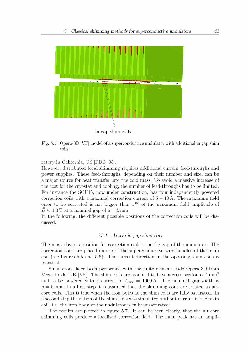
in gap shim coils
Fig. 5.5: Opera-3D [VF] model of a superconductive undulator with additional in gap shimcoils.
ratory in California, US [PDB+05].However, distributed local shimming requires additional current feed-throughs andpower supplies. These feed-throughs, depending on their number and size, can bea major source for heat transfer into the cold mass. To avoid a massive increase ofthe cost for the cryostat and cooling, the number of feed-throughs has to be limited.For instance the SCU15, now under construction, has four independently poweredcorrection coils with a maximal correction current of 5 − 10 A. The maximum fielderror to be corrected is not bigger than 1 % of the maximum field amplitude ofB ≈ 1.3 T at a nominal gap of g = 5 mm.In the following, the different possible positions of the correction coils will be dis-cussed.
5.3.1 Active in gap shim coils
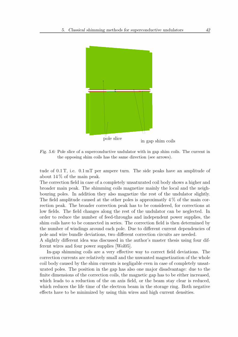
The most obvious position for correction coils is in the gap of the undulator. Thecorrection coils are placed on top of the superconductive wire bundles of the maincoil (see figures 5.5 and 5.6). The current direction in the opposing shim coils isidentical.
Simulations have been performed with the finite element code Opera-3D fromVectorfields, UK [VF]. The shim coils are assumed to have a cross-section of 1 mm2
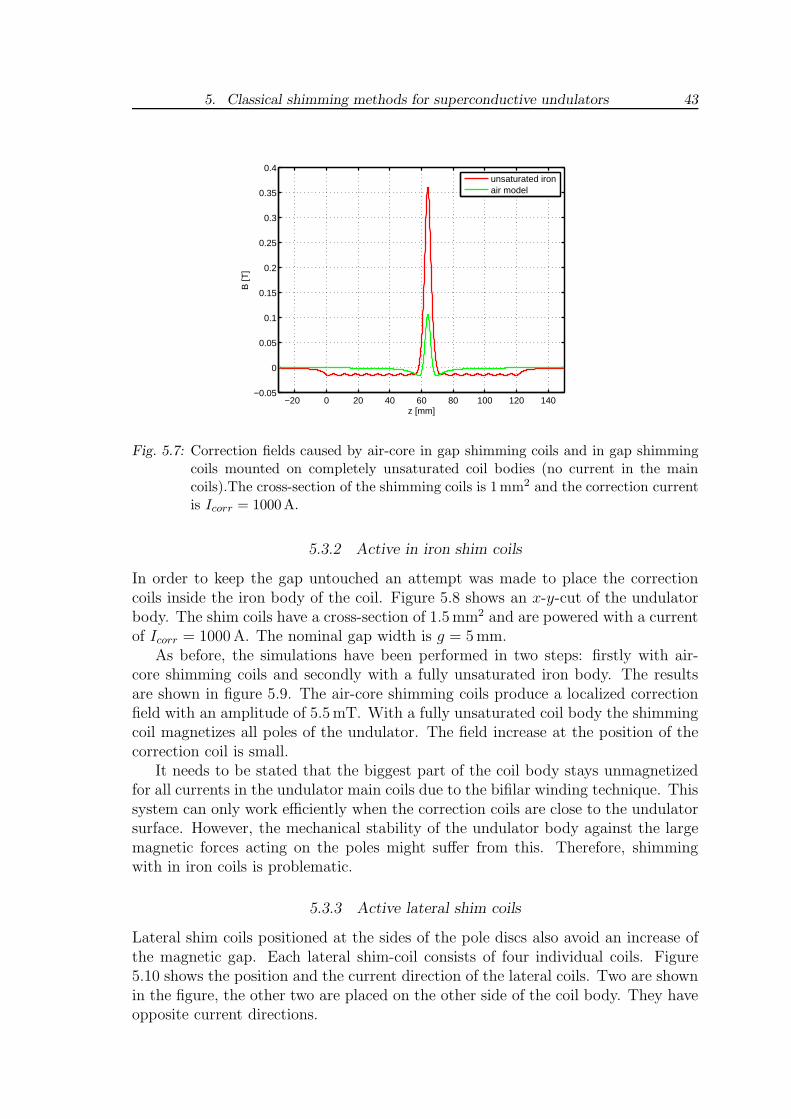
and to be powered with a current of Icorr = 1000 A. The nominal gap width isg = 5 mm. In a first step it is assumed that the shimming coils are treated as air-core coils. This is true when the iron poles at the shim coils are fully saturated. Ina second step the action of the shim coils was simulated without current in the maincoil, i.e. the iron body of the undulator is fully unsaturated.
The results are plotted in figure 5.7. It can be seen clearly, that the air-coreshimming coils produce a localized correction field. The main peak has an ampli-
5. Classical shimming methods for superconductive undulators 42
in gap shim coilspole slice
Fig. 5.6: Pole slice of a superconductive undulator with in gap shim coils. The current inthe opposing shim coils has the same direction (see arrows).
tude of 0.1 T, i.e. 0.1 mT per ampere turn. The side peaks have an amplitude ofabout 14 % of the main peak.The correction field in case of a completely unsaturated coil body shows a higher andbroader main peak. The shimming coils magnetize mainly the local and the neigh-bouring poles. In addition they also magnetize the rest of the undulator slightly.The field amplitude caused at the other poles is approximatly 4 % of the main cor-rection peak. The broader correction peak has to be considered, for corrections atlow fields. The field changes along the rest of the undulator can be neglected. Inorder to reduce the number of feed-throughs and independent power supplies, theshim coils have to be connected in series. The correction field is then determined bythe number of windings around each pole. Due to different current dependencies ofpole and wire bundle deviations, two different correction circuits are needed.A slightly different idea was discussed in the author’s master thesis using four dif-ferent wires and four power supplies [Wol05].
In-gap shimming coils are a very effective way to correct field deviations. Thecorrection currents are relatively small and the unwanted magnetization of the wholecoil body caused by the shim currents is negligable even in case of completely unsat-urated poles. The position in the gap has also one major disadvantage: due to thefinite dimensions of the correction coils, the magnetic gap has to be either increased,which leads to a reduction of the on axis field, or the beam stay clear is reduced,which reduces the life time of the electron beam in the storage ring. Both negativeeffects have to be minimized by using thin wires and high current densities.
5. Classical shimming methods for superconductive undulators 43
−20 0 20 40 60 80 100 120 140−0.05
0
0.05
0.1
0.15
0.2
0.25
0.3
0.35
0.4
z [mm]
B [T
]
unsaturated ironair model
Fig. 5.7: Correction fields caused by air-core in gap shimming coils and in gap shimmingcoils mounted on completely unsaturated coil bodies (no current in the maincoils).The cross-section of the shimming coils is 1mm2 and the correction currentis Icorr = 1000A.
5.3.2 Active in iron shim coils
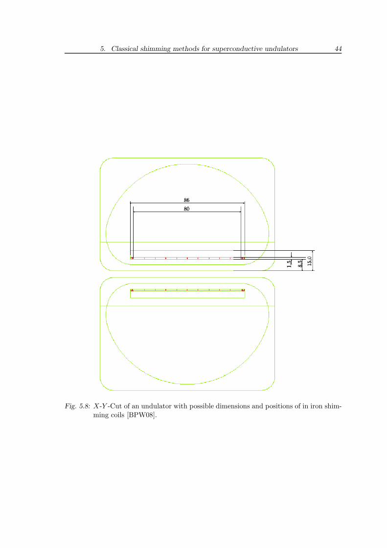
In order to keep the gap untouched an attempt was made to place the correctioncoils inside the iron body of the coil. Figure 5.8 shows an x-y-cut of the undulatorbody. The shim coils have a cross-section of 1.5 mm2 and are powered with a currentof Icorr = 1000 A. The nominal gap width is g = 5 mm.
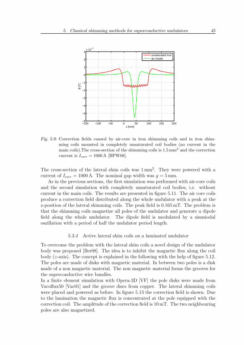
As before, the simulations have been performed in two steps: firstly with air-core shimming coils and secondly with a fully unsaturated iron body. The resultsare shown in figure 5.9. The air-core shimming coils produce a localized correctionfield with an amplitude of 5.5 mT. With a fully unsaturated coil body the shimmingcoil magnetizes all poles of the undulator. The field increase at the position of thecorrection coil is small.
It needs to be stated that the biggest part of the coil body stays unmagnetizedfor all currents in the undulator main coils due to the bifilar winding technique. Thissystem can only work efficiently when the correction coils are close to the undulatorsurface. However, the mechanical stability of the undulator body against the largemagnetic forces acting on the poles might suffer from this. Therefore, shimmingwith in iron coils is problematic.
5.3.3 Active lateral shim coils
Lateral shim coils positioned at the sides of the pole discs also avoid an increase ofthe magnetic gap. Each lateral shim-coil consists of four individual coils. Figure5.10 shows the position and the current direction of the lateral coils. Two are shownin the figure, the other two are placed on the other side of the coil body. They haveopposite current directions.
5. Classical shimming methods for superconductive undulators 44
Fig. 5.8: X-Y -Cut of an undulator with possible dimensions and positions of in iron shim-ming coils [BPW08].
5. Classical shimming methods for superconductive undulators 45
−150 −100 −50 0 50 100 150 200−6
−5
−4
−3
−2
−1
0
1
2
3x 10
−3
z [mm]
B [T
]
unsaturated ironair model
Fig. 5.9: Correction fields caused by air-core in iron shimming coils and in iron shim-ming coils mounted in completely unsaturated coil bodies (no current in themain coils).The cross-section of the shimming coils is 1.5mm2 and the correctioncurrent is Icorr = 1000A [BPW08].
The cross-section of the lateral shim coils was 1 mm2. They were powered with acurrent of Icorr = 1000 A. The nominal gap width was g = 5 mm.
As in the previous sections, the first simulation was performed with air-core coilsand the second simulation with completely unsaturated coil bodies, i.e. withoutcurrent in the main coils. The results are presented in figure 5.11. The air core coilsproduce a correction field distributed along the whole undulator with a peak at thez-position of the lateral shimming coils. The peak field is 0.165 mT. The problem isthat the shimming coils magnetize all poles of the undulator and generate a dipolefield along the whole undulator. The dipole field is modulated by a sinusiodaloszillation with a period of half the undulator period length.
5.3.4 Active lateral shim coils on a laminated undulator
To overcome the problem with the lateral shim coils a novel design of the undulatorbody was proposed [Ber08]. The idea is to inhibit the magnetic flux along the coilbody (z-axis). The concept is explained in the following with the help of figure 5.12.The poles are made of disks with magnetic material. In between two poles is a diskmade of a non magnetic material. The non magnetic material forms the grooves forthe superconductive wire bundles.In a finite element simulation with Opera-3D [VF] the pole disks were made fromVacoflux50 [Vac01] and the groove discs from copper. The lateral shimming coilswere placed and powered as before. In figure 5.13 the correction field is shown. Dueto the lamination the magnetic flux is concentrated at the pole equipped with thecorrection coil. The amplitude of the correction field is 10 mT. The two neighbouringpoles are also magnetized.
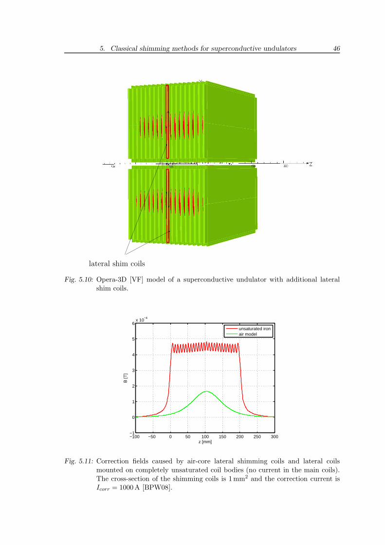
5. Classical shimming methods for superconductive undulators 46
lateral shim coils
Fig. 5.10: Opera-3D [VF] model of a superconductive undulator with additional lateralshim coils.
−100 −50 0 50 100 150 200 250 300−1
0
1
2
3
4
5
6x 10
−4
z [mm]
B [T
]
unsaturated ironair model
Fig. 5.11: Correction fields caused by air-core lateral shimming coils and lateral coilsmounted on completely unsaturated coil bodies (no current in the main coils).The cross-section of the shimming coils is 1mm2 and the correction current isIcorr = 1000A [BPW08].
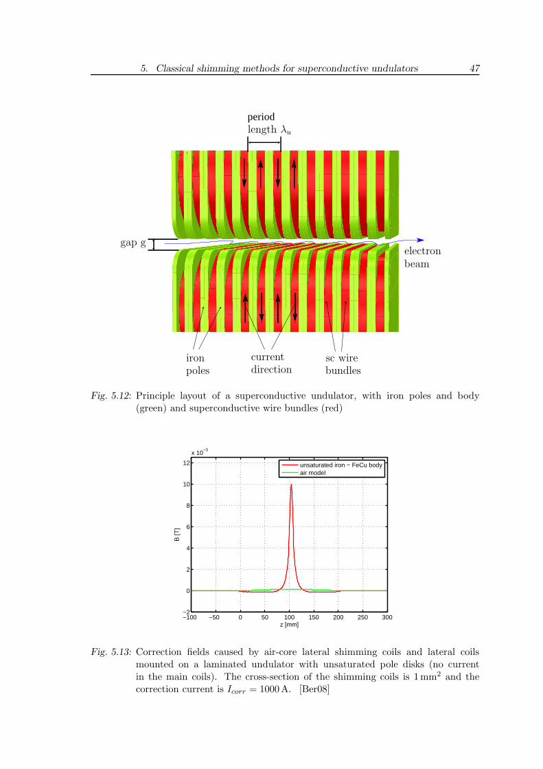
5. Classical shimming methods for superconductive undulators 47
period
ironpoles
currentdirection
sc wirebundles
electronbeam
gap g
length λu
Fig. 5.12: Principle layout of a superconductive undulator, with iron poles and body(green) and superconductive wire bundles (red)
−100 −50 0 50 100 150 200 250 300−2
0
2
4
6
8
10
12
x 10−3
z [mm]
B [T
]
unsaturated iron − FeCu bodyair model
Fig. 5.13: Correction fields caused by air-core lateral shimming coils and lateral coilsmounted on a laminated undulator with unsaturated pole disks (no currentin the main coils). The cross-section of the shimming coils is 1mm2 and thecorrection current is Icorr = 1000A. [Ber08]

5. Classical shimming methods for superconductive undulators 48
For a laminated undulator lateral shimming coils are an effective way to correctfield deviations since the shimming coils are outside the gap at the side of theundulator. The position outside the gap has the disadvantage, that the requiredcorrection currents or the number of windings in the lateral coils are higher. Theunwanted magnetization of the whole coil body is inhibited by the laminated design.
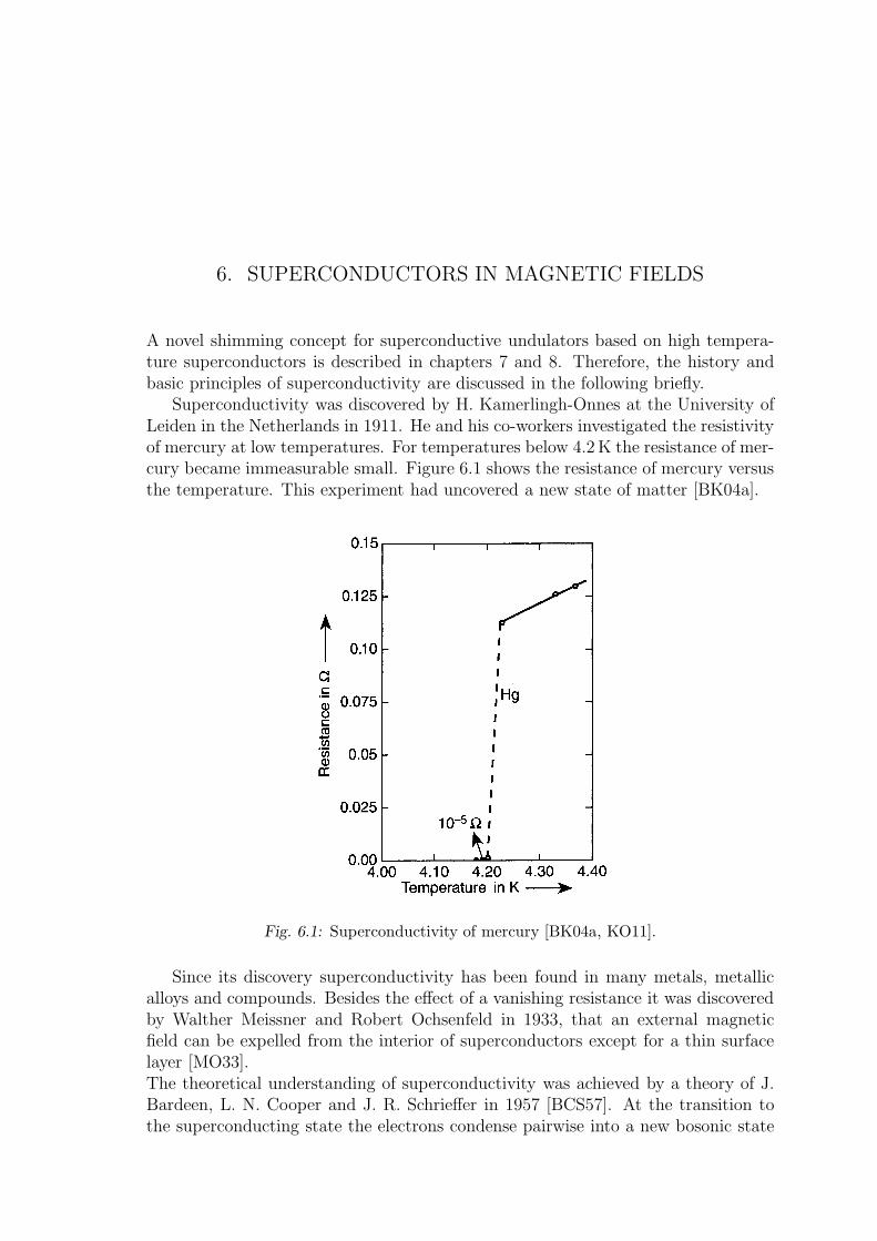
6. SUPERCONDUCTORS IN MAGNETIC FIELDS
A novel shimming concept for superconductive undulators based on high tempera-ture superconductors is described in chapters 7 and 8. Therefore, the history andbasic principles of superconductivity are discussed in the following briefly.
Superconductivity was discovered by H. Kamerlingh-Onnes at the University ofLeiden in the Netherlands in 1911. He and his co-workers investigated the resistivityof mercury at low temperatures. For temperatures below 4.2 K the resistance of mer-cury became immeasurable small. Figure 6.1 shows the resistance of mercury versusthe temperature. This experiment had uncovered a new state of matter [BK04a].
Fig. 6.1: Superconductivity of mercury [BK04a, KO11].
Since its discovery superconductivity has been found in many metals, metallicalloys and compounds. Besides the effect of a vanishing resistance it was discoveredby Walther Meissner and Robert Ochsenfeld in 1933, that an external magneticfield can be expelled from the interior of superconductors except for a thin surfacelayer [MO33].The theoretical understanding of superconductivity was achieved by a theory of J.Bardeen, L. N. Cooper and J. R. Schrieffer in 1957 [BCS57]. At the transition tothe superconducting state the electrons condense pairwise into a new bosonic state
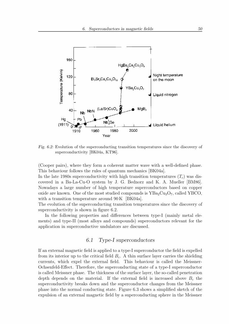
6. Superconductors in magnetic fields 50
Fig. 6.2: Evolution of the superconducting transition temperatures since the discovery ofsuperconductivity [BK04a, KT96].
(Cooper pairs), where they form a coherent matter wave with a well-defined phase.This behaviour follows the rules of quantum mechanics [BK04a].In the late 1980s superconductivity with high transition temperatures (Tc) was dis-covered in a Ba-La-Cu-O system by J. G. Bednorz and K. A. Mueller [BM86].Nowadays a large number of high temperature superconductors based on copperoxide are known. One of the most studied compounds is YBa2Cu3O7, called YBCO,with a transition temperature around 90 K [BK04a].The evolution of the superconducting transition temperatures since the discovery ofsuperconductivity is shown in figure 6.2.
In the following properties and differences between type-I (mainly metal ele-ments) and type-II (most alloys and compounds) superconductors relevant for theapplication in superconductive undulators are discussed.
6.1 Type-I superconductors
If an external magnetic field is applied to a type-I superconductor the field is expelledfrom its interior up to the critical field Bc. A thin surface layer carries the shieldingcurrents, which expel the external field. This behaviour is called the Meissner-Ochsenfeld-Effect. Therefore, the superconducting state of a type-I superconductoris called Meissner phase. The thickness of the surface layer, the so-called penetrationdepth depends on the material. If the external field is increased above Bc thesuperconductivity breaks down and the superconductor changes from the Meissnerphase into the normal conducting state. Figure 6.3 shows a simplified sketch of theexpulsion of an external magnetic field by a superconducting sphere in the Meissner
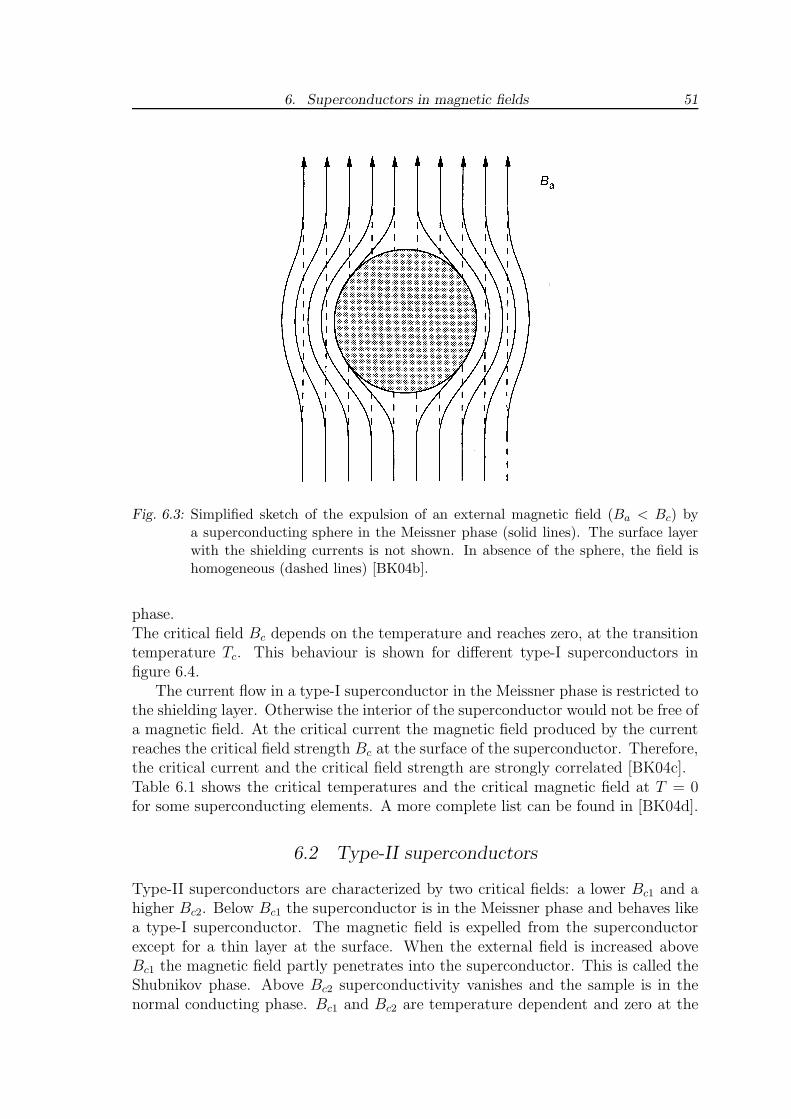
6. Superconductors in magnetic fields 51
Fig. 6.3: Simplified sketch of the expulsion of an external magnetic field (Ba < Bc) bya superconducting sphere in the Meissner phase (solid lines). The surface layerwith the shielding currents is not shown. In absence of the sphere, the field ishomogeneous (dashed lines) [BK04b].
phase.The critical field Bc depends on the temperature and reaches zero, at the transitiontemperature Tc. This behaviour is shown for different type-I superconductors infigure 6.4.
The current flow in a type-I superconductor in the Meissner phase is restricted tothe shielding layer. Otherwise the interior of the superconductor would not be free ofa magnetic field. At the critical current the magnetic field produced by the currentreaches the critical field strength Bc at the surface of the superconductor. Therefore,the critical current and the critical field strength are strongly correlated [BK04c].Table 6.1 shows the critical temperatures and the critical magnetic field at T = 0for some superconducting elements. A more complete list can be found in [BK04d].
6.2 Type-II superconductors
Type-II superconductors are characterized by two critical fields: a lower Bc1 and ahigher Bc2. Below Bc1 the superconductor is in the Meissner phase and behaves likea type-I superconductor. The magnetic field is expelled from the superconductorexcept for a thin layer at the surface. When the external field is increased aboveBc1 the magnetic field partly penetrates into the superconductor. This is called theShubnikov phase. Above Bc2 superconductivity vanishes and the sample is in thenormal conducting phase. Bc1 and Bc2 are temperature dependent and zero at the
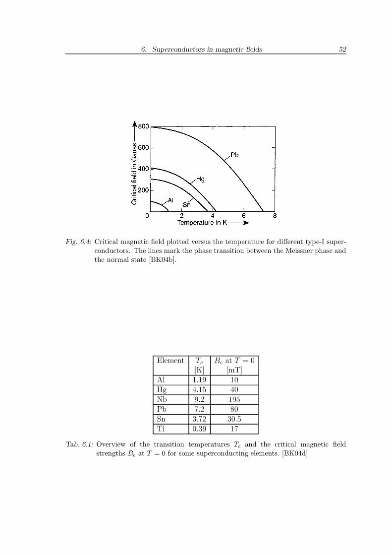
6. Superconductors in magnetic fields 52
Fig. 6.4: Critical magnetic field plotted versus the temperature for different type-I super-conductors. The lines mark the phase transition between the Meissner phase andthe normal state [BK04b].
Element Tc Bc at T = 0[K] [mT]
Al 1.19 10Hg 4.15 40Nb 9.2 195Pb 7.2 80Sn 3.72 30.5Ti 0.39 17
Tab. 6.1: Overview of the transition temperatures Tc and the critical magnetic fieldstrengths Bc at T = 0 for some superconducting elements. [BK04d]
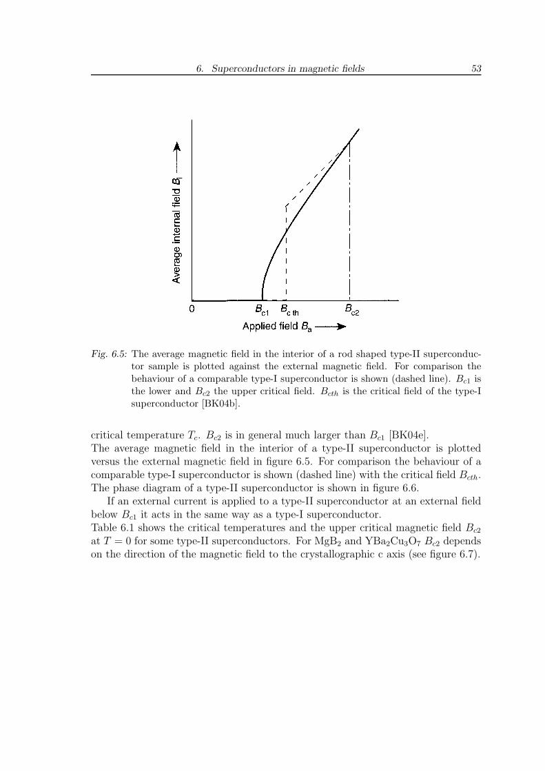
6. Superconductors in magnetic fields 53
Fig. 6.5: The average magnetic field in the interior of a rod shaped type-II superconduc-tor sample is plotted against the external magnetic field. For comparison thebehaviour of a comparable type-I superconductor is shown (dashed line). Bc1 isthe lower and Bc2 the upper critical field. Bcth is the critical field of the type-Isuperconductor [BK04b].
critical temperature Tc. Bc2 is in general much larger than Bc1 [BK04e].The average magnetic field in the interior of a type-II superconductor is plottedversus the external magnetic field in figure 6.5. For comparison the behaviour of acomparable type-I superconductor is shown (dashed line) with the critical field Bcth.The phase diagram of a type-II superconductor is shown in figure 6.6.
If an external current is applied to a type-II superconductor at an external fieldbelow Bc1 it acts in the same way as a type-I superconductor.Table 6.1 shows the critical temperatures and the upper critical magnetic field Bc2
at T = 0 for some type-II superconductors. For MgB2 and YBa2Cu3O7 Bc2 dependson the direction of the magnetic field to the crystallographic c axis (see figure 6.7).
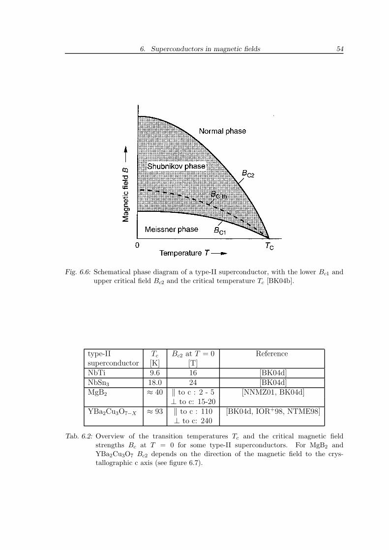
6. Superconductors in magnetic fields 54
Fig. 6.6: Schematical phase diagram of a type-II superconductor, with the lower Bc1 andupper critical field Bc2 and the critical temperature Tc [BK04b].
type-II Tc Bc2 at T = 0 Referencesuperconductor [K] [T]NbTi 9.6 16 [BK04d]NbSn3 18.0 24 [BK04d]MgB2 ≈ 40 ‖ to c : 2 - 5 [NNMZ01, BK04d]
⊥ to c: 15-20YBa2Cu3O7−X ≈ 93 ‖ to c : 110 [BK04d, IOR+98, NTME98]
⊥ to c: 240
Tab. 6.2: Overview of the transition temperatures Tc and the critical magnetic fieldstrengths Bc at T = 0 for some type-II superconductors. For MgB2 andYBa2Cu3O7 Bc2 depends on the direction of the magnetic field to the crys-tallographic c axis (see figure 6.7).
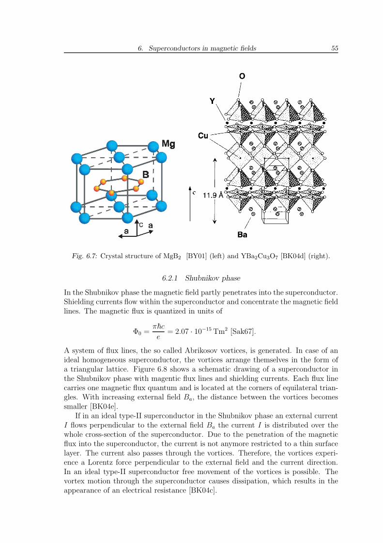
6. Superconductors in magnetic fields 55
Fig. 6.7: Crystal structure of MgB2 [BY01] (left) and YBa2Cu3O7 [BK04d] (right).
6.2.1 Shubnikov phase
In the Shubnikov phase the magnetic field partly penetrates into the superconductor.Shielding currents flow within the superconductor and concentrate the magnetic fieldlines. The magnetic flux is quantized in units of
Φ0 =π~c
e= 2.07 · 10−15 Tm2 [Sak67].
A system of flux lines, the so called Abrikosov vortices, is generated. In case of anideal homogeneous superconductor, the vortices arrange themselves in the form ofa triangular lattice. Figure 6.8 shows a schematic drawing of a superconductor inthe Shubnikov phase with magentic flux lines and shielding currents. Each flux linecarries one magnetic flux quantum and is located at the corners of equilateral trian-gles. With increasing external field Ba, the distance between the vortices becomessmaller [BK04e].
If in an ideal type-II superconductor in the Shubnikov phase an external currentI flows perpendicular to the external field Ba the current I is distributed over thewhole cross-section of the superconductor. Due to the penetration of the magneticflux into the superconductor, the current is not anymore restricted to a thin surfacelayer. The current also passes through the vortices. Therefore, the vortices experi-ence a Lorentz force perpendicular to the external field and the current direction.In an ideal type-II superconductor free movement of the vortices is possible. Thevortex motion through the superconductor causes dissipation, which results in theappearance of an electrical resistance [BK04c].
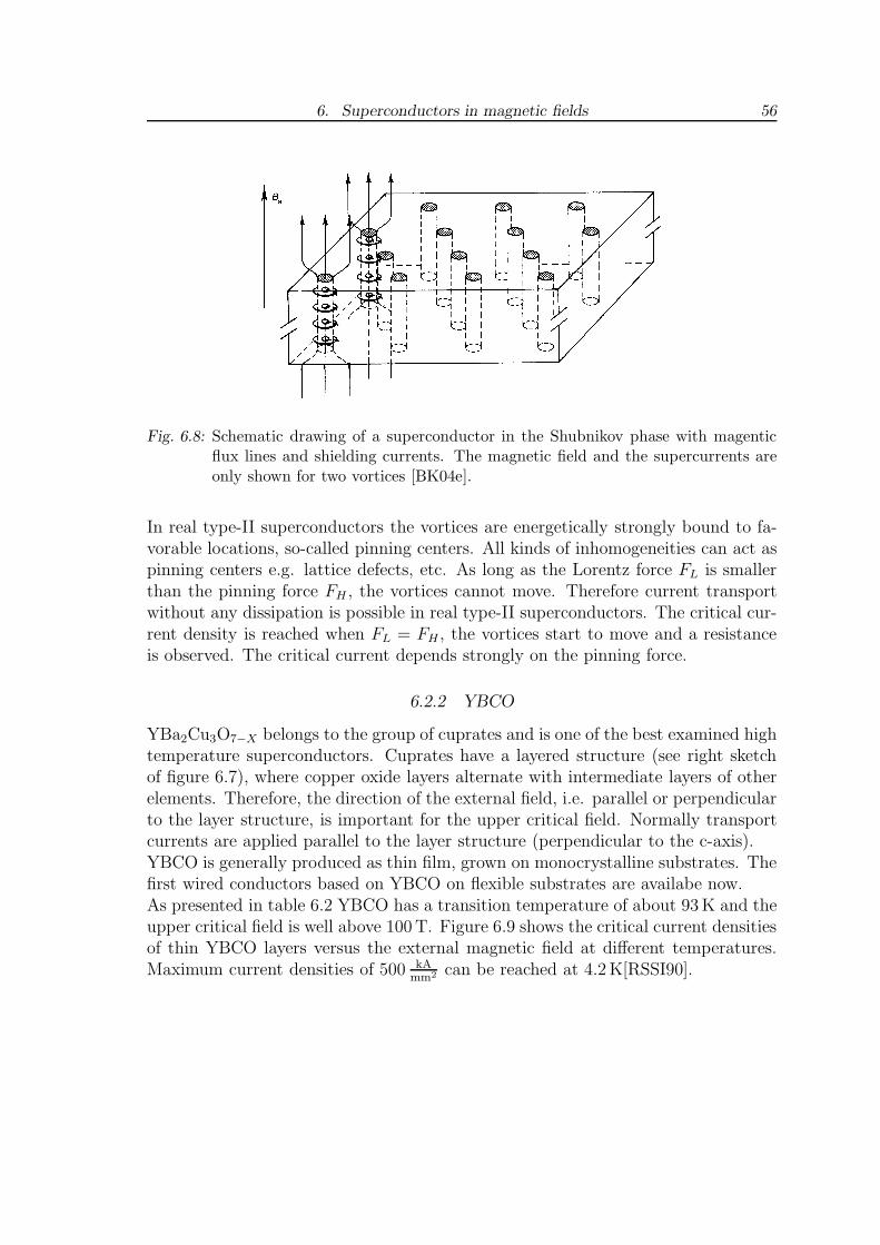
6. Superconductors in magnetic fields 56
Fig. 6.8: Schematic drawing of a superconductor in the Shubnikov phase with magenticflux lines and shielding currents. The magnetic field and the supercurrents areonly shown for two vortices [BK04e].
In real type-II superconductors the vortices are energetically strongly bound to fa-vorable locations, so-called pinning centers. All kinds of inhomogeneities can act aspinning centers e.g. lattice defects, etc. As long as the Lorentz force FL is smallerthan the pinning force FH , the vortices cannot move. Therefore current transportwithout any dissipation is possible in real type-II superconductors. The critical cur-rent density is reached when FL = FH , the vortices start to move and a resistanceis observed. The critical current depends strongly on the pinning force.
6.2.2 YBCO
YBa2Cu3O7−X belongs to the group of cuprates and is one of the best examined hightemperature superconductors. Cuprates have a layered structure (see right sketchof figure 6.7), where copper oxide layers alternate with intermediate layers of otherelements. Therefore, the direction of the external field, i.e. parallel or perpendicularto the layer structure, is important for the upper critical field. Normally transportcurrents are applied parallel to the layer structure (perpendicular to the c-axis).YBCO is generally produced as thin film, grown on monocrystalline substrates. Thefirst wired conductors based on YBCO on flexible substrates are availabe now.As presented in table 6.2 YBCO has a transition temperature of about 93 K and theupper critical field is well above 100 T. Figure 6.9 shows the critical current densitiesof thin YBCO layers versus the external magnetic field at different temperatures.Maximum current densities of 500 kA
mm2 can be reached at 4.2 K[RSSI90].
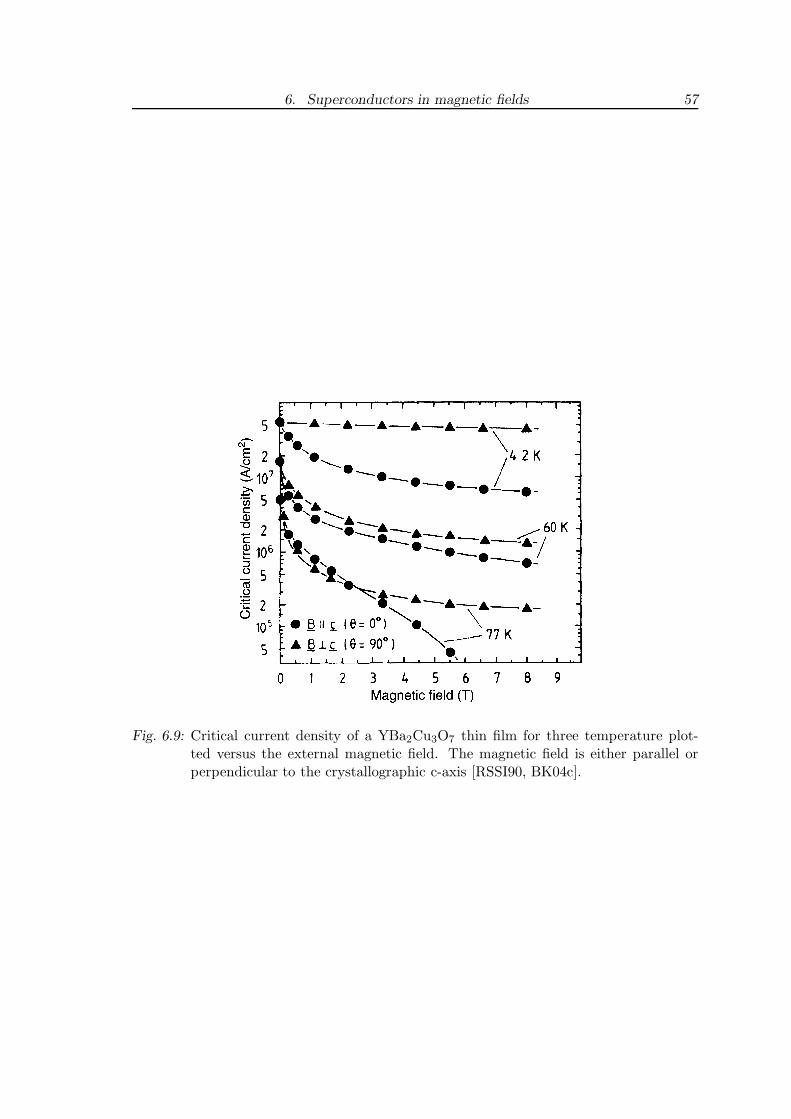
6. Superconductors in magnetic fields 57
Fig. 6.9: Critical current density of a YBa2Cu3O7 thin film for three temperature plot-ted versus the external magnetic field. The magnetic field is either parallel orperpendicular to the crystallographic c-axis [RSSI90, BK04c].
7. INDUCTION SHIMMING: CONCEPT
Shimming of undulators is a time consuming procedure for permanent magnet, cryo-genic or superconductive undulators. It has to be performed iteratively: field mea-surement, field correction and verification. This procedure means for superconduc-tive undulators that the coils have to be cooled down and warmed up several times.Active shimming concepts always require additional current feed-throughs, whichcomplicate the design of the cryostat and increase the heat transfer to the coldmass. Therefore only a small number of individually powered correction coils canbe used for active shimming.Active shimming becomes even more complex, due to the different current depen-dencies of the field errors caused by the different types of mechanical deviations.Moreover, the errors caused by the iron are subject to hysteresis and require com-plex correction algorithms.
Therefore, in the following a passive shimming concept is presented, which cancorrect field errors automatically [WBR08, WBP+08c].
7.1 Induction-shimming: Theory
The induction shimming concept is based on Faraday’s law of induction
∮
C
Ed~l = −d
dt
∫
S
Bd ~A, (7.1)
where B is the magnetic flux density over the area S enclosed by the contour C. E
is the electrical field strength. Using an ideal conductor along the contour, i.e. asuperconductive closed loop, equation (7.1) is reduced to
0 =d
dt
∫
S
Bd ~A. (7.2)
This means that the change in magnetic flux through the closed loop is inhibited bythe induced current [KSW00].To demonstrate the basic principle a uniform magnetic field is considered in a firststep.
7.1.1 One period with closed-loop
Assume a superconductive loop positioned on the beam-sided surface of an undulatorcoil. The width of the superconductive closed loop in the beam direction is one period
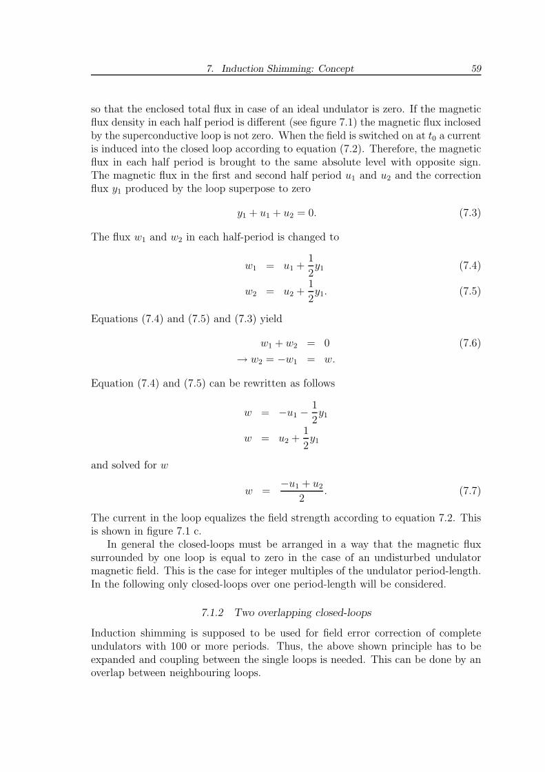
7. Induction Shimming: Concept 59
so that the enclosed total flux in case of an ideal undulator is zero. If the magneticflux density in each half period is different (see figure 7.1) the magnetic flux inclosedby the superconductive loop is not zero. When the field is switched on at t0 a currentis induced into the closed loop according to equation (7.2). Therefore, the magneticflux in each half period is brought to the same absolute level with opposite sign.The magnetic flux in the first and second half period u1 and u2 and the correctionflux y1 produced by the loop superpose to zero
y1 + u1 + u2 = 0. (7.3)
The flux w1 and w2 in each half-period is changed to
w1 = u1 +1
2y1 (7.4)
w2 = u2 +1
2y1. (7.5)
Equations (7.4) and (7.5) and (7.3) yield
w1 + w2 = 0 (7.6)
→ w2 = −w1 = w.
Equation (7.4) and (7.5) can be rewritten as follows
w = −u1 −1
2y1
w = u2 +1
2y1
and solved for w
w =−u1 + u2
2. (7.7)
The current in the loop equalizes the field strength according to equation 7.2. Thisis shown in figure 7.1 c.
In general the closed-loops must be arranged in a way that the magnetic fluxsurrounded by one loop is equal to zero in the case of an undisturbed undulatormagnetic field. This is the case for integer multiples of the undulator period-length.In the following only closed-loops over one period-length will be considered.
7.1.2 Two overlapping closed-loops
Induction shimming is supposed to be used for field error correction of completeundulators with 100 or more periods. Thus, the above shown principle has to beexpanded and coupling between the single loops is needed. This can be done by anoverlap between neighbouring loops.
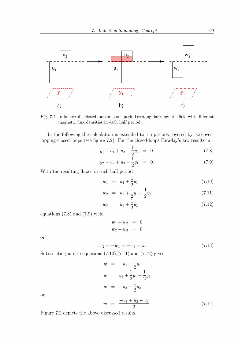
7. Induction Shimming: Concept 60
y1
u1
u2
y1
u1
u2
y1
1w
2w
a) b) c)
Fig. 7.1: Influence of a closed loop on a one period rectangular magnetic field with differentmagnetic flux densities in each half period.
In the following the calculation is extended to 1.5 periods covered by two over-lapping closed loops (see figure 7.2). For the closed-loops Faraday’s law results in
y1 + u1 + u2 +1
2y2 = 0 (7.8)
y2 + u2 + u3 +1
2y1 = 0. (7.9)
With the resulting fluxes in each half period
w1 = u1 +1
2y1 (7.10)
w2 = u2 +1
2y1 +
1
2y2 (7.11)
w3 = u3 +1
2y2 (7.12)
equations (7.8) and (7.9) yield
w1 + w2 = 0
w2 + w3 = 0
or
w2 = −w1 = −w3 = w. (7.13)
Substituting w into equations (7.10),(7.11) and (7.12) gives
w = −u1 −1
2y1
w = u2 +1
2y1 +
1
2y2
w = −u3 −1
2y2
or
w =−u1 + u2 − u3
3. (7.14)
Figure 7.2 depicts the above discussed results.
7. Induction Shimming: Concept 61
w
w w
y1y2
u1
u2
u3
y1y2
2
1 3
y1y2
u1
u2
u3
b) c)a)
Fig. 7.2: Behaviour of two overlapping closed-loops in a rectangular magnetic field withdifferent field amplitudes.
u1
u2
u3
u4
u5
un−3
un−2
un−1 un+1
un
yn−2yn−3 yn−1 yny4
y3y1 y2
Fig. 7.3: Rectangular field with n + 1 half periods and n overlapping closed loops
7.1.3 Generalization for n closed-loops
In the following the induction-shimming concept with superconductive closed-loopsis extended to n closed-loopsThe system is shown in figure 7.3, with the magnetic flux un in the n-th half-period (n = 1, 2, 3, ...), the correction flux ym produced by the closed-loop m (m =1, 2, 3, ..., n − 1) and the resulting fluxes wn.
The set of equations for Faraday’s law can than be written as
y1 + u1 + u2 +1
2y2 = 0
y2 + u2 + u3 +1
2y1 +
1
2y3 = 0
...
yn−1 + un−1 + un +1
2yn−2 +
1
2yn = 0
yn + un + un+1 +1
2yn−1 = 0. (7.15)
7. Induction Shimming: Concept 62
The magnetic flux in each half period is
w1 = u1 +1
2y1
w2 = u2 +1
2y1 +
1
2y2
...
wn = un +1
2yn−1 +
1
2yn
wn+1 = un+1 +1
2yn. (7.16)
Substituting these equations into the closed-loop equations (7.15) gives
w1 + w2 = 0
w2 + w3 = 0...
wn−1 + wn = 0
wn + wn+1 = 0,
which is equal to
w = ±w1 = ∓w2 = ... = ±wn = ∓wn+1. (7.17)
The magnetic flux in each half period becomes
w = ±u1 ±1
2y1
w = ∓u2 ∓1
2y1 ∓
1
2y2
...
w = ±un ±1
2yn−1 ±
1
2yn
w = ∓un+1 ∓1
2yn,
which can be solved for w:
w =±u1 ∓ u2 ± . . . ± un ∓ un+1
n + 1. (7.18)
As with the one and two loop systems described before, the system of n overlappingclosed-loops adjusts the absolute values of the magnetic flux in each half period tothe same level.
7.2 Generalization for Biot-Savart closed-loops
In the following the concept is extended to sinusoidal fields and the field producedby the current in the loops is described by the law of Biot-Savart.
7. Induction Shimming: Concept 63
For the sake of simplicity the closed-loops are considered to consist of ideally super-conducting long straight wires perpendicular to the beam direction (z-axis). Theloop parts parallel to the e-beam direction can be neglected due to their large dis-tance from the e-beam.
7.2.1 Faraday’s law for overlapping closed-loops in a long undulator
Faraday’s law of induction (see equation (7.1)) for one closed-loop can be written as
I = −1
LΦ. (7.19)
Where Φ is the time derivative of the magnetic flux through the closed-loop, L isthe self-inductance of the loop and I the time derivative of the induced current. Foran induction-shimming scheme with overlapping closed loops the coupling betweenthe loops also has to be considered. The coupling between loop i and loop j with amutual inductance Mij is defined by
Ii = Mij Ij . (7.20)
Combining equation (7.19) and (7.20) and solving for Φ gives
Φi = L
(
∑
j 6=i
Mij Ij − Ii
)
. (7.21)
When the current in the undulator main coil is turned on at the time t0 the fluxthrough the closed-loops is changed from zero to a certain value and a current I isinduced. Integration of equation (7.21) yields
Φi = L
(
∑
j 6=i
MijIj − Ii
)
. (7.22)
The self-inductance L and the mutual inductances Mij are defined by the geometricalarrangement and the design of the closed-loops.
7.2.2 Biot-Savart’s law for overlapping closed-loops in a long undulator
In a real superconductive undulator a set of overlapping closed-loops will be mountedin the way shown in figure 7.4. The undulator consists of N periods and the shim-ming system of 2N − 1 closed-loops. The loops are numbered from the entrance ofthe undulator (1,2,...,2N-1). Errors of the undulator magnetic field induce correc-tion currents in the closed-loops. The main field and the correction fields superposein the beam plane. For this arrangement of superconductive closed-loops the self-inductance and the mutual inductances will be determined in the following with thehelp of Biot-Savart’s law.
7. Induction Shimming: Concept 64
e−
z
y
closed loop correction coils
Fig. 7.4: Cross section of an undulator with the main coils (green: iron; red: superconduc-tive wire-bundles) and overlapping closed-loops for correction (magenta) placedclose to the main coils.
λu
I
wcc
hcc
Fig. 7.5: One closed-loop made out of two long straight wires .
The magnitude of the magnetic flux density B at a point P at the distanceR =
√
z2 + y2 caused by a current I in a long straight wire, running parallel to thex-axis, is given by [Jac99b]
|B| =µ0
4πIR
∫ ∞
−∞
dl
(R2 + l2)3/2=
µ0
2π
I
R. (7.23)
µ0 = 4π · 10−7 VsAm
is the magnetic permeability in vacuum. The coordinate systemis defined in figure 7.4.With cos α = z
Rand the above definition of R the y-component of the magnetic flux
density at a point P can be calculated as
By(y, z) = |B| cosα =µ0I
2π
z
z2 + y2. (7.24)
Where z and y are the distances from the center of the conductor to point P . Theconductor has the dimensions wcc × hcc.
Treating this as a two dimensional problem the magnetic flux produced by theloop shown in figure 7.5 is
Φ = 2 ·
∫ λu−32wcc
wcc/2
By(z′)dz′ = 2 ·
µ0I
2π
∫ λu−32wcc
wcc/2
1
z′dz′
= 2 ·µ0
4π· I
(
ln(λu −
32wcc)
2
(wcc
2)2
)
= −L · I. (7.25)
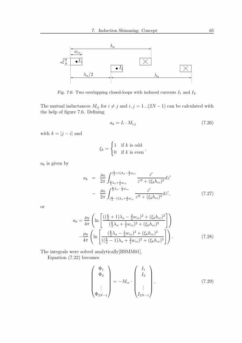
7. Induction Shimming: Concept 65
λu
λu
λu/2
I1
I2
wcc
hcc
Fig. 7.6: Two overlapping closed-loops with induced currents I1 and I2.
The mutual inductances Mij for i 6= j and i, j = 1...(2N − 1) can be calculated withthe help of figure 7.6. Defining
ak = L · Mi,j (7.26)
with k = |j − i| and
ξk =
{
1 if k is odd
0 if k is even,
ak is given by
ak =µ0
2π
∫ (k2+1)λu−
32wcc
k2λu+ 1
2wcc
z′
z′2 + (ξkhcc)2dz′
−µ0
2π
∫ k2λu−
12wcc
(k2−1)λu+ 3
2wcc
z′
z′2 + (ξkhcc)2dz′, (7.27)
or
ak =µ0
4π
(
ln
[
((k2
+ 1)λu −32wcc)
2 + (ξkhcc)2
(k2λu + 1
2wcc)2 + (ξkhcc)2
])
−µ0
4π
(
ln
[
(k2λu −
12wcc)
2 + (ξkhcc)2
((k2− 1)λu + 3
2wcc)2 + (ξkhcc)2
])
. (7.28)
The integrals were solved analytically[BSMM01].Equation (7.22) becomes
Φ1
Φ2
...Φ2N−1
= −Mcc ·
I1
I2
...I2N−1
, (7.29)
7. Induction Shimming: Concept 66
with the symmetrical matrix
Mcc =
L a1 a2 · · · a2N−1
a1. . .
...
a2. . . a2
.... . . a1
a2N−1 · · · a2 a1 L
, (7.30)
The resulting magnetic field along the beam axis can be written in the form
By(z) = By,main(z) +
2N−1∑
l=1
By,l(z), (7.31)
where By,main(z) is the magnetic field along the beam axis generated by the undu-lator main coils and By,l(z) is the field generated by the closed-loop l (see equation(7.24)).
7.3 Simulations
In the following it is assumed that the magnetic field is sinusoidal. Amplitude andperiod-length can be varied in each half period. The mid-plane of the supercon-ductive closed-loops is considered to be 1 mm away from the source (main coil) and2.5 mm from the beam plane. The undisturbed field amplitude on axis is 1 T.
7.3.1 Correction of a single field-error
For a first simulation a three period undulator has been modelled with a 10% toohigh second maximum. A single pole, which is closer to the beam than the oth-ers would cause this error. The field plot along the beam axis with and withoutinduction-shimming is shown in figure 7.7. The second maximum was reduced byabout 7% from 1.1 T to 1.03 T. The absolute values of the neighbouring minimawere increased to 1.025 T and the first maximum was increased to 1.015 T. Thechanges in the third maximum and minimum were negligible. The error previouslylocalized in one half period was reduced and distributed over two periods.The comparisons of the first and the second field integrals with and without induction-shimming are shown in figure 7.8. The final value of the first field integral was re-duced by a factor of two and the sign changed. The final value of the second fieldintegral was reduced by 15%.Considering an additional region of ten periods, i.e. 140 mm, at each side of theundulator, the final values of the first field integral converge. This is shown in figure7.9. The correction of the first field integral is only locally.
7.3.2 Monte-Carlo simulations
As discussed in chapter 3 mechanical deviations are the main reasons for phase errorsin superconductive undulators. Therefore it is important to examine the influence of
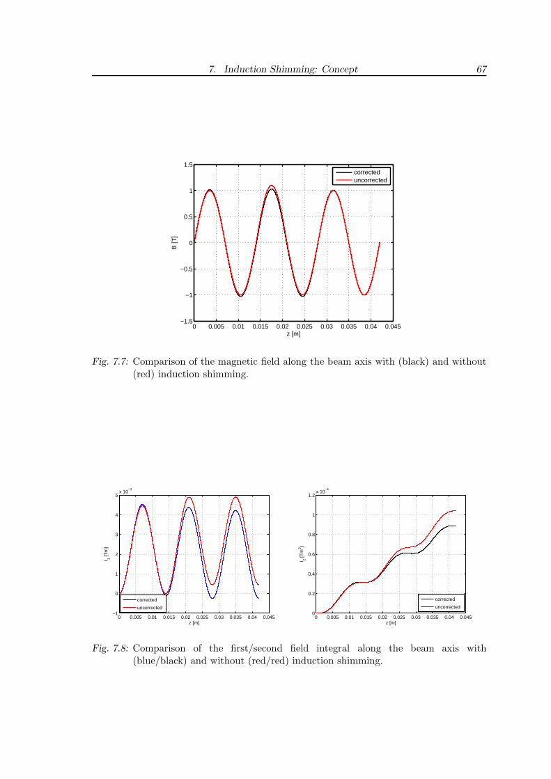
7. Induction Shimming: Concept 67
0 0.005 0.01 0.015 0.02 0.025 0.03 0.035 0.04 0.045−1.5
−1
−0.5
0
0.5
1
1.5
z [m]
B [T
]
correcteduncorrected
Fig. 7.7: Comparison of the magnetic field along the beam axis with (black) and without(red) induction shimming.
0 0.005 0.01 0.015 0.02 0.025 0.03 0.035 0.04 0.045−1
0
1
2
3
4
5x 10
−3
z [m]
I 1 [Tm
]
corrected
uncorrected
0 0.005 0.01 0.015 0.02 0.025 0.03 0.035 0.04 0.0450
0.2
0.4
0.6
0.8
1
1.2x 10
−4
z [m]
I 2 [Tm
2 ]
corrected
uncorrected
Fig. 7.8: Comparison of the first/second field integral along the beam axis with(blue/black) and without (red/red) induction shimming.
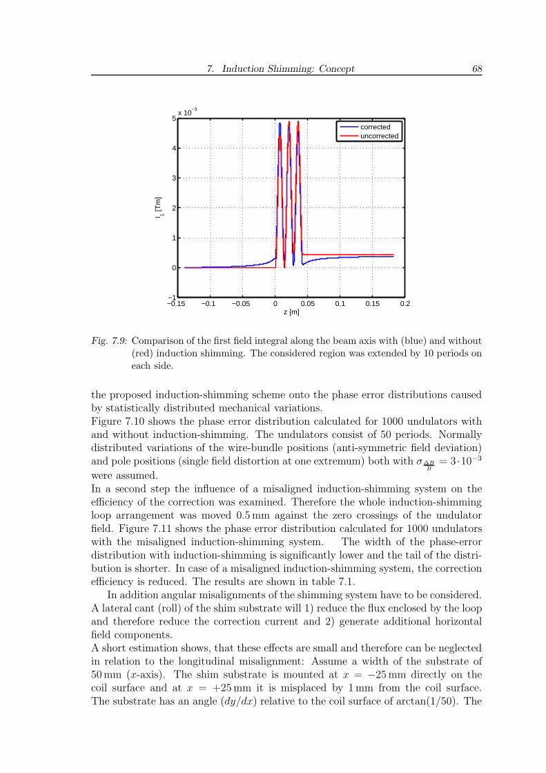
7. Induction Shimming: Concept 68
−0.15 −0.1 −0.05 0 0.05 0.1 0.15 0.2−1
0
1
2
3
4
5x 10
−3
z [m]
I 1 [Tm
]
correcteduncorrected
Fig. 7.9: Comparison of the first field integral along the beam axis with (blue) and without(red) induction shimming. The considered region was extended by 10 periods oneach side.
the proposed induction-shimming scheme onto the phase error distributions causedby statistically distributed mechanical variations.Figure 7.10 shows the phase error distribution calculated for 1000 undulators withand without induction-shimming. The undulators consist of 50 periods. Normallydistributed variations of the wire-bundle positions (anti-symmetric field deviation)and pole positions (single field distortion at one extremum) both with σ∆B
B= 3 ·10−3
were assumed.In a second step the influence of a misaligned induction-shimming system on theefficiency of the correction was examined. Therefore the whole induction-shimmingloop arrangement was moved 0.5 mm against the zero crossings of the undulatorfield. Figure 7.11 shows the phase error distribution calculated for 1000 undulatorswith the misaligned induction-shimming system. The width of the phase-errordistribution with induction-shimming is significantly lower and the tail of the distri-bution is shorter. In case of a misaligned induction-shimming system, the correctionefficiency is reduced. The results are shown in table 7.1.
In addition angular misalignments of the shimming system have to be considered.A lateral cant (roll) of the shim substrate will 1) reduce the flux enclosed by the loopand therefore reduce the correction current and 2) generate additional horizontalfield components.A short estimation shows, that these effects are small and therefore can be neglectedin relation to the longitudinal misalignment: Assume a width of the substrate of50 mm (x-axis). The shim substrate is mounted at x = −25 mm directly on thecoil surface and at x = +25 mm it is misplaced by 1 mm from the coil surface.The substrate has an angle (dy/dx) relative to the coil surface of arctan(1/50). The
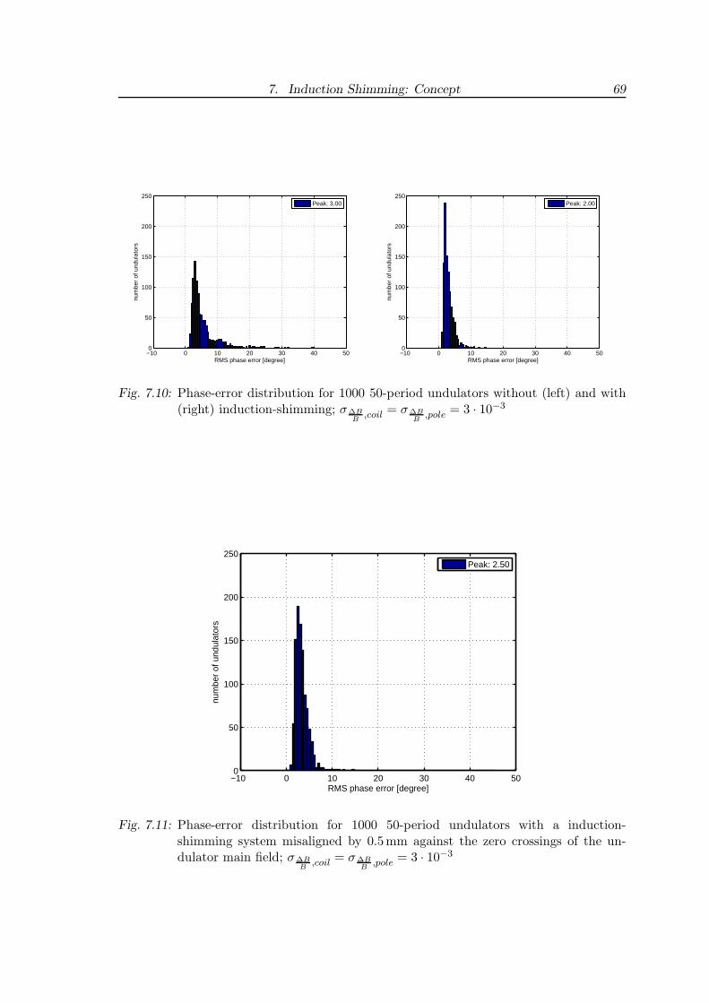
7. Induction Shimming: Concept 69
−10 0 10 20 30 40 500
50
100
150
200
250
RMS phase error [degree]
num
ber
of u
ndul
ator
s
Peak: 3.00
−10 0 10 20 30 40 500
50
100
150
200
250
RMS phase error [degree]
num
ber
of u
ndul
ator
s
Peak: 2.00
Fig. 7.10: Phase-error distribution for 1000 50-period undulators without (left) and with(right) induction-shimming; σ∆B
B,coil = σ∆B
B,pole = 3 · 10−3
−10 0 10 20 30 40 500
50
100
150
200
250
RMS phase error [degree]
num
ber
of u
ndul
ator
s
Peak: 2.50
Fig. 7.11: Phase-error distribution for 1000 50-period undulators with a induction-shimming system misaligned by 0.5mm against the zero crossings of the un-dulator main field; σ∆B
B,coil = σ∆B
B,pole = 3 · 10−3
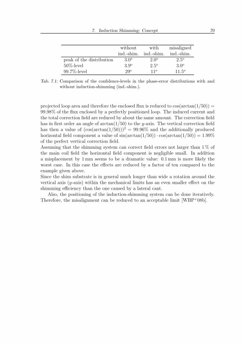
7. Induction Shimming: Concept 70
without with misalignedind.-shim. ind.-shim. ind.-shim.
peak of the distribution 3.0o 2.0o 2.5o
50%-level 3.9o 2.5o 3.0o
99.7%-level 29o 11o 11.5o
Tab. 7.1: Comparison of the confidence-levels in the phase-error distributions with andwithout induction-shimming (ind.-shim.).
projected loop area and therefore the enclosed flux is reduced to cos(arctan(1/50)) =99.98% of the flux enclosed by a perfectly positioned loop. The induced current andthe total correction field are reduced by about the same amount. The correction fieldhas in first order an angle of arctan(1/50) to the y-axis. The vertical correction fieldhas then a value of (cos(arctan(1/50)))2 = 99.96% and the additionally producedhorizontal field component a value of sin(arctan(1/50)) · cos(arctan(1/50)) = 1.99%of the perfect vertical correction field.Assuming that the shimming system can correct field errors not larger than 1 % ofthe main coil field the horizontal field component is negligible small. In additiona misplacement by 1 mm seems to be a dramatic value: 0.1 mm is more likely theworst case. In this case the effects are reduced by a factor of ten compared to theexample given above.Since the shim substrate is in general much longer than wide a rotation around thevertical axis (y-axis) within the mechanical limits has an even smaller effect on theshimming efficiency than the one caused by a lateral cant.
Also, the positioning of the induction-shimming system can be done iteratively.Therefore, the misalignment can be reduced to an acceptable limit [WBP+08b].
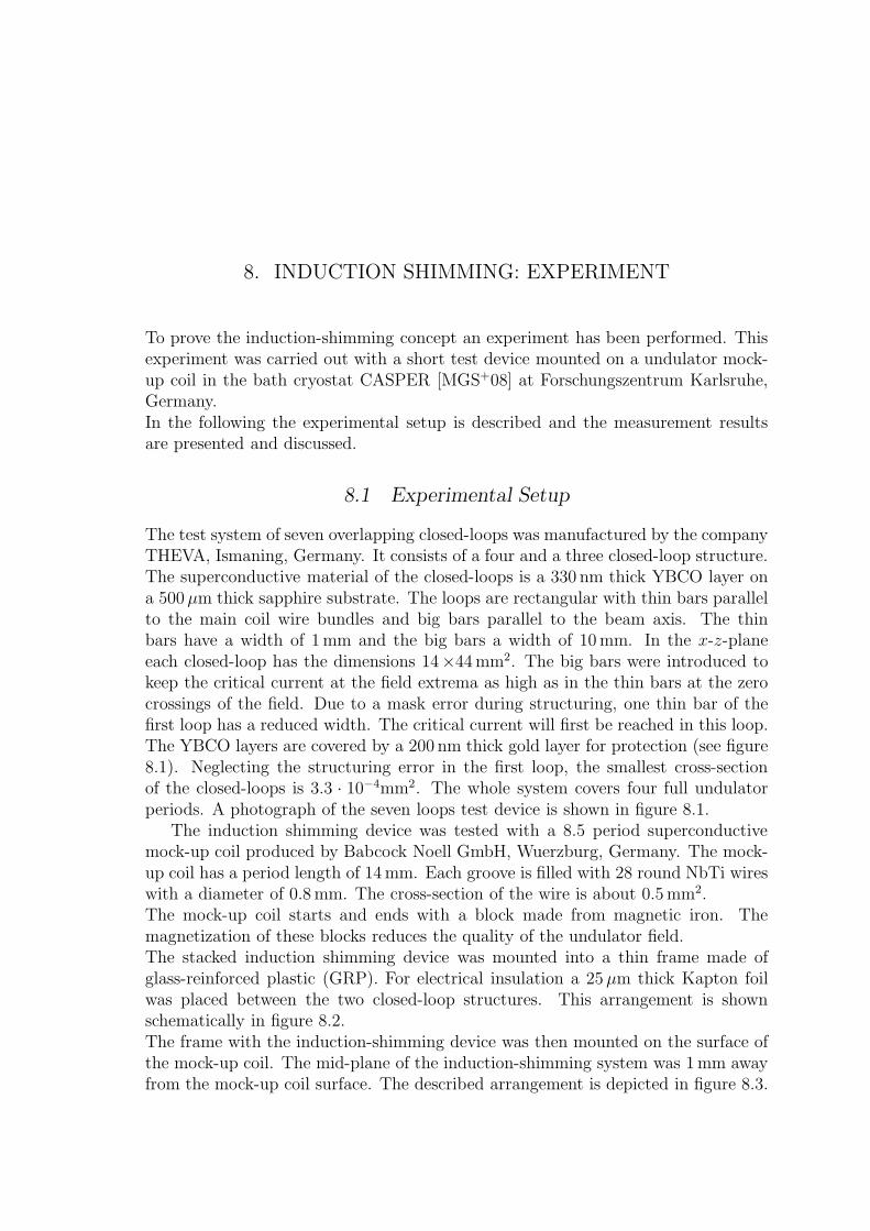
8. INDUCTION SHIMMING: EXPERIMENT
To prove the induction-shimming concept an experiment has been performed. Thisexperiment was carried out with a short test device mounted on a undulator mock-up coil in the bath cryostat CASPER [MGS+08] at Forschungszentrum Karlsruhe,Germany.In the following the experimental setup is described and the measurement resultsare presented and discussed.
8.1 Experimental Setup
The test system of seven overlapping closed-loops was manufactured by the companyTHEVA, Ismaning, Germany. It consists of a four and a three closed-loop structure.The superconductive material of the closed-loops is a 330 nm thick YBCO layer ona 500 µm thick sapphire substrate. The loops are rectangular with thin bars parallelto the main coil wire bundles and big bars parallel to the beam axis. The thinbars have a width of 1 mm and the big bars a width of 10 mm. In the x-z-planeeach closed-loop has the dimensions 14×44 mm2. The big bars were introduced tokeep the critical current at the field extrema as high as in the thin bars at the zerocrossings of the field. Due to a mask error during structuring, one thin bar of thefirst loop has a reduced width. The critical current will first be reached in this loop.The YBCO layers are covered by a 200 nm thick gold layer for protection (see figure8.1). Neglecting the structuring error in the first loop, the smallest cross-sectionof the closed-loops is 3.3 · 10−4mm2. The whole system covers four full undulatorperiods. A photograph of the seven loops test device is shown in figure 8.1.
The induction shimming device was tested with a 8.5 period superconductivemock-up coil produced by Babcock Noell GmbH, Wuerzburg, Germany. The mock-up coil has a period length of 14 mm. Each groove is filled with 28 round NbTi wireswith a diameter of 0.8 mm. The cross-section of the wire is about 0.5 mm2.The mock-up coil starts and ends with a block made from magnetic iron. Themagnetization of these blocks reduces the quality of the undulator field.The stacked induction shimming device was mounted into a thin frame made ofglass-reinforced plastic (GRP). For electrical insulation a 25 µm thick Kapton foilwas placed between the two closed-loop structures. This arrangement is shownschematically in figure 8.2.The frame with the induction-shimming device was then mounted on the surface ofthe mock-up coil. The mid-plane of the induction-shimming system was 1 mm awayfrom the mock-up coil surface. The described arrangement is depicted in figure 8.3.
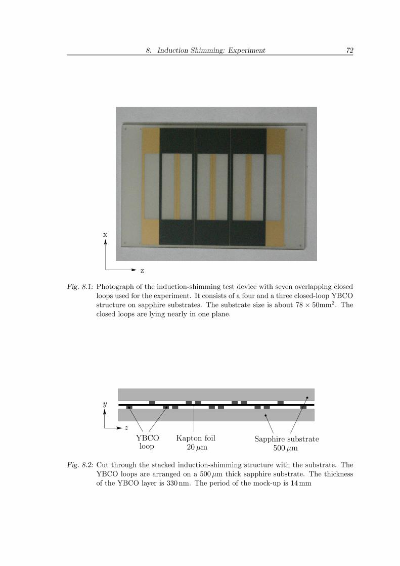
8. Induction Shimming: Experiment 72
z
x
Fig. 8.1: Photograph of the induction-shimming test device with seven overlapping closedloops used for the experiment. It consists of a four and a three closed-loop YBCOstructure on sapphire substrates. The substrate size is about 78 × 50mm2. Theclosed loops are lying nearly in one plane.
z
y
YBCOloop
Kapton foil20 µm
Sapphire substrate500 µm
Fig. 8.2: Cut through the stacked induction-shimming structure with the substrate. TheYBCO loops are arranged on a 500µm thick sapphire substrate. The thicknessof the YBCO layer is 330 nm. The period of the mock-up is 14mm
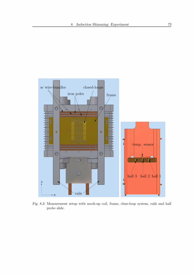
8. Induction Shimming: Experiment 73
z
x rails
closed-loops
frame
sc wire-bundles
iron poles
hall 1hall 2hall 3
temp. sensor
Fig. 8.3: Measurement setup with mock-up coil, frame, close-loop system, rails and hallprobe slide.
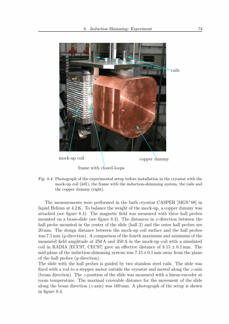
8. Induction Shimming: Experiment 74
rails
frame with closed-loops
mock-up coil copper dummy
Fig. 8.4: Photograph of the experimental setup before installation in the cryostat with themock-up coil (left), the frame with the induction-shimming system, the rails andthe copper dummy (right).
The measurements were performed in the bath cryostat CASPER [MGS+08] inliquid Helium at 4.2 K. To balance the weight of the mock-up, a copper dummy wasattached (see figure 8.4). The magnetic field was measured with three hall probesmounted on a brass-slide (see figure 8.3). The distances in x-direction between thehall probe mounted in the center of the slide (hall 2) and the outer hall probes are20 mm. The design distance between the mock-up coil surface and the hall probeswas 7.5 mm (y-direction). A comparison of the fourth maximum and minimum of themeasured field amplitude at 250 A and 350 A in the mock-up coil with a simulatedcoil in RADIA [ECC97, CEC97] gave an effective distance of 8.15 ± 0.1 mm. Themid-plane of the induction-shimming system was 7.15±0.1 mm away from the planeof the hall probes (y-direction).The slide with the hall probes is guided by two stainless steel rails. The slide wasfixed with a rod to a stepper motor outside the cryostat and moved along the z-axis(beam direction). The z-position of the slide was measured with a linear-encoder atroom temperature. The maximal coverable distance for the movement of the slidealong the beam direction (z-axis) was 169 mm. A photograph of the setup is shownin figure 8.4.
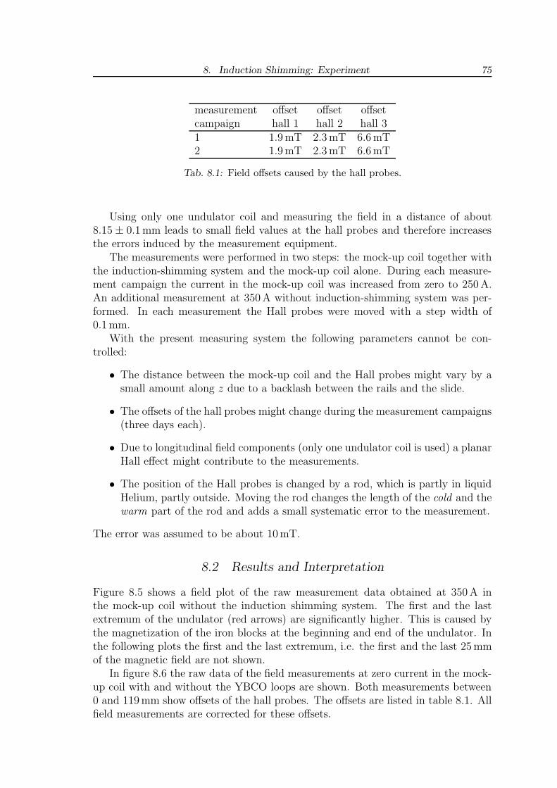
8. Induction Shimming: Experiment 75
measurement offset offset offsetcampaign hall 1 hall 2 hall 31 1.9 mT 2.3 mT 6.6 mT2 1.9 mT 2.3 mT 6.6 mT
Tab. 8.1: Field offsets caused by the hall probes.
Using only one undulator coil and measuring the field in a distance of about8.15 ± 0.1 mm leads to small field values at the hall probes and therefore increasesthe errors induced by the measurement equipment.
The measurements were performed in two steps: the mock-up coil together withthe induction-shimming system and the mock-up coil alone. During each measure-ment campaign the current in the mock-up coil was increased from zero to 250 A.An additional measurement at 350 A without induction-shimming system was per-formed. In each measurement the Hall probes were moved with a step width of0.1 mm.
With the present measuring system the following parameters cannot be con-trolled:
• The distance between the mock-up coil and the Hall probes might vary by asmall amount along z due to a backlash between the rails and the slide.
• The offsets of the hall probes might change during the measurement campaigns(three days each).
• Due to longitudinal field components (only one undulator coil is used) a planarHall effect might contribute to the measurements.
• The position of the Hall probes is changed by a rod, which is partly in liquidHelium, partly outside. Moving the rod changes the length of the cold and thewarm part of the rod and adds a small systematic error to the measurement.
The error was assumed to be about 10 mT.
8.2 Results and Interpretation
Figure 8.5 shows a field plot of the raw measurement data obtained at 350 A inthe mock-up coil without the induction shimming system. The first and the lastextremum of the undulator (red arrows) are significantly higher. This is caused bythe magnetization of the iron blocks at the beginning and end of the undulator. Inthe following plots the first and the last extremum, i.e. the first and the last 25 mmof the magnetic field are not shown.
In figure 8.6 the raw data of the field measurements at zero current in the mock-up coil with and without the YBCO loops are shown. Both measurements between0 and 119 mm show offsets of the hall probes. The offsets are listed in table 8.1. Allfield measurements are corrected for these offsets.
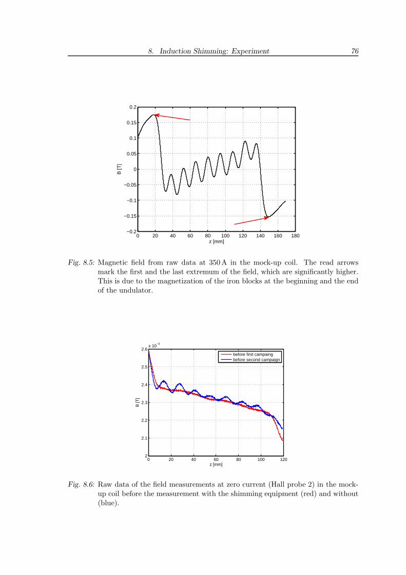
8. Induction Shimming: Experiment 76
0 20 40 60 80 100 120 140 160 180−0.2
−0.15
−0.1
−0.05
0
0.05
0.1
0.15
0.2
z [mm]
B [T
]
Fig. 8.5: Magnetic field from raw data at 350A in the mock-up coil. The read arrowsmark the first and the last extremum of the field, which are significantly higher.This is due to the magnetization of the iron blocks at the beginning and the endof the undulator.
0 20 40 60 80 100 1202
2.1
2.2
2.3
2.4
2.5
2.6x 10
−3
z [mm]
B [T
]
before first campaingbefore second campaign
Fig. 8.6: Raw data of the field measurements at zero current (Hall probe 2) in the mock-up coil before the measurement with the shimming equipment (red) and without(blue).
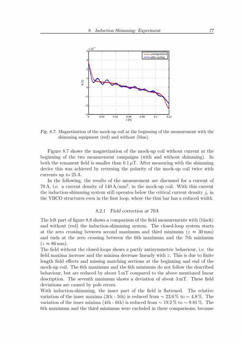
8. Induction Shimming: Experiment 77
0 0.02 0.04 0.06 0.08 0.1 0.12−3
−2
−1
0
1
2
3
4x 10
−4
z [m]
B [T
]
unmagnetizedafter cycling
Fig. 8.7: Magnetization of the mock-up coil at the beginning of the measurement with theshimming equipment (red) and without (blue).
Figure 8.7 shows the magnetization of the mock-up coil without current at thebeginning of the two measurement campaigns (with and without shimming). Inboth the remanent field is smaller than 0.1 µT. After measuring with the shimmingdevice this was achieved by reversing the polarity of the mock-up coil twice withcurrents up to 25 A.
In the following, the results of the measurement are discussed for a current of70 A, i.e. a current density of 140 A/mm2, in the mock-up coil. With this currentthe induction-shimming system still operates below the critical current density jc inthe YBCO structures even in the first loop, where the thin bar has a reduced width.
8.2.1 Field correction at 70A
The left part of figure 8.8 shows a comparison of the field measurements with (black)and without (red) the induction-shimming system. The closed-loop system startsat the zero crossing between second maximum and third minimum (z ≈ 30 mm)and ends at the zero crossing between the 6th maximum and the 7th minimum(z ≈ 86 mm).The field without the closed-loops shows a partly antisymmetric behaviour, i.e. thefield maxima increase and the minima decrease linearly with z. This is due to finitelength field effects and missing matching sections at the beginning and end of themock-up coil. The 6th maximum and the 6th minimum do not follow the describedbehaviour, but are reduced by about 5 mT compared to the above mentioned lineardescription. The seventh minimum shows a deviation of about 3 mT. These fielddeviations are caused by pole errors.With induction-shimming, the inner part of the field is flattened. The relativevariation of the inner maxima (3th - 5th) is reduced from ∼ 23.6 % to ∼ 4.8 %. Thevariation of the inner minima (4th - 6th) is reduced from ∼ 19.2 % to ∼ 9.81 %. The6th maximum and the third minimum were excluded in these comparisons, because
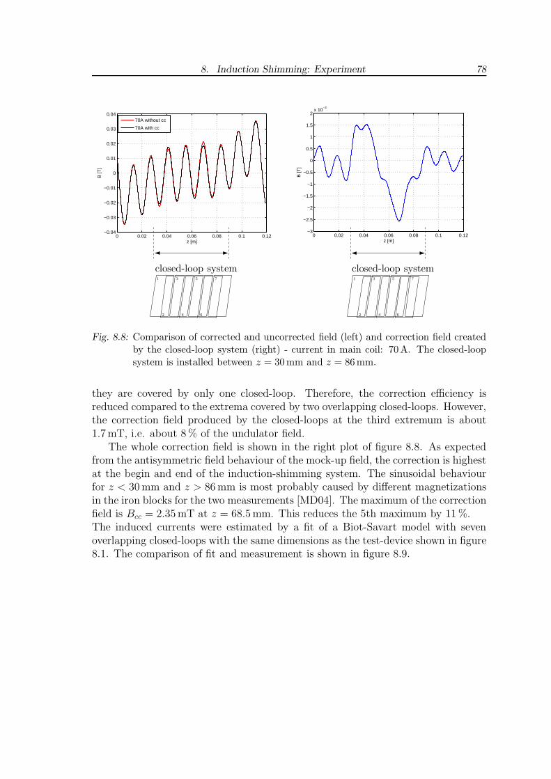
8. Induction Shimming: Experiment 78
0 0.02 0.04 0.06 0.08 0.1 0.12−0.04
−0.03
−0.02
−0.01
0
0.01
0.02
0.03
0.04
z [m]
B [T
]
70A without cc
70A with cc
2
31
4 6
5 7
closed-loop system3 5 7
642
1
0 0.02 0.04 0.06 0.08 0.1 0.12−3
−2.5
−2
−1.5
−1
−0.5
0
0.5
1
1.5
2x 10
−3
z [m]
B [T
]
closed-loop system
Fig. 8.8: Comparison of corrected and uncorrected field (left) and correction field createdby the closed-loop system (right) - current in main coil: 70A. The closed-loopsystem is installed between z = 30mm and z = 86mm.
they are covered by only one closed-loop. Therefore, the correction efficiency isreduced compared to the extrema covered by two overlapping closed-loops. However,the correction field produced by the closed-loops at the third extremum is about1.7 mT, i.e. about 8 % of the undulator field.
The whole correction field is shown in the right plot of figure 8.8. As expectedfrom the antisymmetric field behaviour of the mock-up field, the correction is highestat the begin and end of the induction-shimming system. The sinusoidal behaviourfor z < 30 mm and z > 86 mm is most probably caused by different magnetizationsin the iron blocks for the two measurements [MD04]. The maximum of the correctionfield is Bcc = 2.35 mT at z = 68.5 mm. This reduces the 5th maximum by 11 %.The induced currents were estimated by a fit of a Biot-Savart model with sevenoverlapping closed-loops with the same dimensions as the test-device shown in figure8.1. The comparison of fit and measurement is shown in figure 8.9.
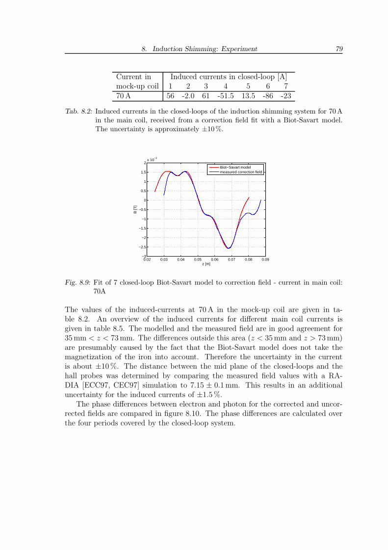
8. Induction Shimming: Experiment 79
Current in Induced currents in closed-loop [A]mock-up coil 1 2 3 4 5 6 770 A 56 -2.0 61 -51.5 13.5 -86 -23
Tab. 8.2: Induced currents in the closed-loops of the induction shimming system for 70Ain the main coil, received from a correction field fit with a Biot-Savart model.The uncertainty is approximately ±10%.
0.02 0.03 0.04 0.05 0.06 0.07 0.08 0.09−3
−2.5
−2
−1.5
−1
−0.5
0
0.5
1
1.5
2x 10
−3
z [m]
B [T
]
Biot−Savart modelmeasured correction field
Fig. 8.9: Fit of 7 closed-loop Biot-Savart model to correction field - current in main coil:70A
The values of the induced-currents at 70 A in the mock-up coil are given in ta-ble 8.2. An overview of the induced currents for different main coil currents isgiven in table 8.5. The modelled and the measured field are in good agreement for35 mm < z < 73 mm. The differences outside this area (z < 35 mm and z > 73 mm)are presumably caused by the fact that the Biot-Savart model does not take themagnetization of the iron into account. Therefore the uncertainty in the currentis about ±10 %. The distance between the mid plane of the closed-loops and thehall probes was determined by comparing the measured field values with a RA-DIA [ECC97, CEC97] simulation to 7.15 ± 0.1 mm. This results in an additionaluncertainty for the induced currents of ±1.5 %.
The phase differences between electron and photon for the corrected and uncor-rected fields are compared in figure 8.10. The phase differences are calculated overthe four periods covered by the closed-loop system.
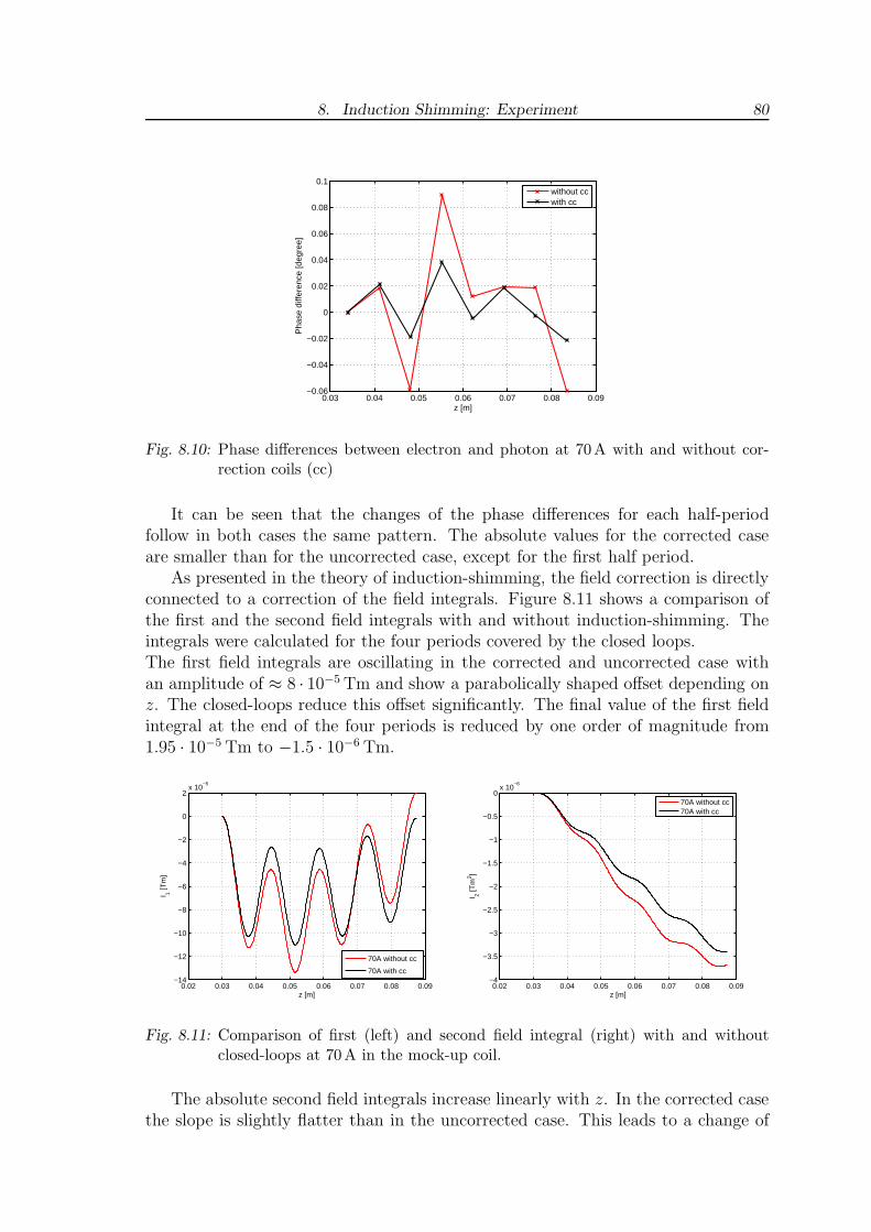
8. Induction Shimming: Experiment 80
0.03 0.04 0.05 0.06 0.07 0.08 0.09−0.06
−0.04
−0.02
0
0.02
0.04
0.06
0.08
0.1
z [m]
Pha
se d
iffer
ence
[deg
ree]
without ccwith cc
Fig. 8.10: Phase differences between electron and photon at 70A with and without cor-rection coils (cc)
It can be seen that the changes of the phase differences for each half-periodfollow in both cases the same pattern. The absolute values for the corrected caseare smaller than for the uncorrected case, except for the first half period.
As presented in the theory of induction-shimming, the field correction is directlyconnected to a correction of the field integrals. Figure 8.11 shows a comparison ofthe first and the second field integrals with and without induction-shimming. Theintegrals were calculated for the four periods covered by the closed loops.The first field integrals are oscillating in the corrected and uncorrected case withan amplitude of ≈ 8 · 10−5 Tm and show a parabolically shaped offset depending onz. The closed-loops reduce this offset significantly. The final value of the first fieldintegral at the end of the four periods is reduced by one order of magnitude from1.95 · 10−5 Tm to −1.5 · 10−6 Tm.
0.02 0.03 0.04 0.05 0.06 0.07 0.08 0.09−14
−12
−10
−8
−6
−4
−2
0
2x 10
−5
z [m]
I 1 [Tm
]
70A without cc
70A with cc
0.02 0.03 0.04 0.05 0.06 0.07 0.08 0.09−4
−3.5
−3
−2.5
−2
−1.5
−1
−0.5
0x 10
−6
z [m]
I 2 [Tm
2 ]
70A without cc70A with cc
Fig. 8.11: Comparison of first (left) and second field integral (right) with and withoutclosed-loops at 70A in the mock-up coil.
The absolute second field integrals increase linearly with z. In the corrected casethe slope is slightly flatter than in the uncorrected case. This leads to a change of
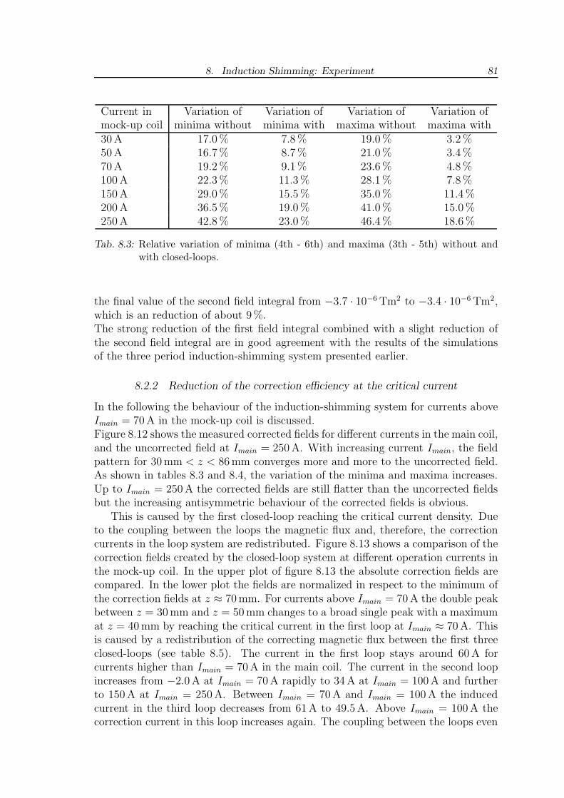
8. Induction Shimming: Experiment 81
Current in Variation of Variation of Variation of Variation ofmock-up coil minima without minima with maxima without maxima with30 A 17.0 % 7.8 % 19.0 % 3.2 %50 A 16.7 % 8.7 % 21.0 % 3.4 %70 A 19.2 % 9.1 % 23.6 % 4.8 %100 A 22.3 % 11.3 % 28.1 % 7.8 %150 A 29.0 % 15.5 % 35.0 % 11.4 %200 A 36.5 % 19.0 % 41.0 % 15.0 %250 A 42.8 % 23.0 % 46.4 % 18.6 %
Tab. 8.3: Relative variation of minima (4th - 6th) and maxima (3th - 5th) without andwith closed-loops.
the final value of the second field integral from −3.7 · 10−6 Tm2 to −3.4 · 10−6 Tm2,which is an reduction of about 9 %.The strong reduction of the first field integral combined with a slight reduction ofthe second field integral are in good agreement with the results of the simulationsof the three period induction-shimming system presented earlier.
8.2.2 Reduction of the correction efficiency at the critical current
In the following the behaviour of the induction-shimming system for currents aboveImain = 70 A in the mock-up coil is discussed.Figure 8.12 shows the measured corrected fields for different currents in the main coil,and the uncorrected field at Imain = 250 A. With increasing current Imain, the fieldpattern for 30 mm < z < 86 mm converges more and more to the uncorrected field.As shown in tables 8.3 and 8.4, the variation of the minima and maxima increases.Up to Imain = 250 A the corrected fields are still flatter than the uncorrected fieldsbut the increasing antisymmetric behaviour of the corrected fields is obvious.
This is caused by the first closed-loop reaching the critical current density. Dueto the coupling between the loops the magnetic flux and, therefore, the correctioncurrents in the loop system are redistributed. Figure 8.13 shows a comparison of thecorrection fields created by the closed-loop system at different operation currents inthe mock-up coil. In the upper plot of figure 8.13 the absolute correction fields arecompared. In the lower plot the fields are normalized in respect to the minimum ofthe correction fields at z ≈ 70 mm. For currents above Imain = 70 A the double peakbetween z = 30 mm and z = 50 mm changes to a broad single peak with a maximumat z = 40 mm by reaching the critical current in the first loop at Imain ≈ 70 A. Thisis caused by a redistribution of the correcting magnetic flux between the first threeclosed-loops (see table 8.5). The current in the first loop stays around 60 A forcurrents higher than Imain = 70 A in the main coil. The current in the second loopincreases from −2.0 A at Imain = 70 A rapidly to 34 A at Imain = 100 A and furtherto 150 A at Imain = 250 A. Between Imain = 70 A and Imain = 100 A the inducedcurrent in the third loop decreases from 61 A to 49.5 A. Above Imain = 100 A thecorrection current in this loop increases again. The coupling between the loops even
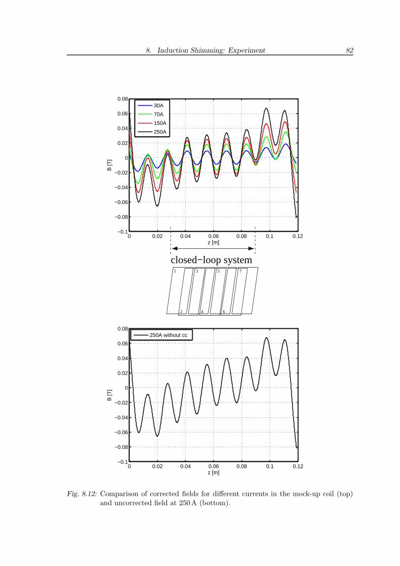
8. Induction Shimming: Experiment 82
0 0.02 0.04 0.06 0.08 0.1 0.12−0.1
−0.08
−0.06
−0.04
−0.02
0
0.02
0.04
0.06
0.08
z [m]
B [T
]
30A
70A
150A
250A
closed−loop system7
642
31 5
0 0.02 0.04 0.06 0.08 0.1 0.12−0.1
−0.08
−0.06
−0.04
−0.02
0
0.02
0.04
0.06
0.08
z [m]
B [T
]
250A without cc
Fig. 8.12: Comparison of corrected fields for different currents in the mock-up coil (top)and uncorrected field at 250A (bottom).
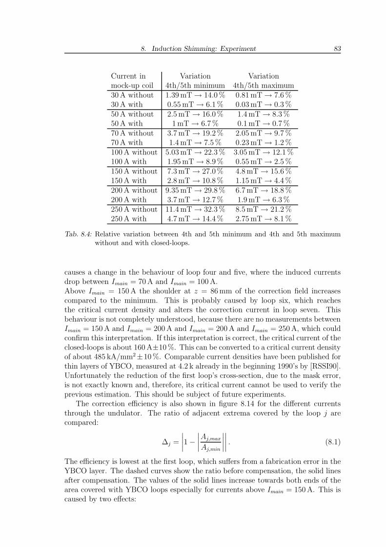
8. Induction Shimming: Experiment 83
Current in Variation Variationmock-up coil 4th/5th minimum 4th/5th maximum30 A without 1.39 mT → 14.0 % 0.81 mT → 7.6 %30 A with 0.55 mT → 6.1 % 0.03 mT → 0.3 %50 A without 2.5 mT → 16.0 % 1.4 mT → 8.3 %50 A with 1 mT → 6.7 % 0.1 mT → 0.7 %70 A without 3.7 mT → 19.2 % 2.05 mT → 9.7 %70 A with 1.4 mT → 7.5 % 0.23 mT → 1.2 %100 A without 5.03 mT → 22.3 % 3.05 mT → 12.1 %100 A with 1.95 mT → 8.9 % 0.55 mT → 2.5 %150 A without 7.3 mT → 27.0 % 4.8 mT → 15.6 %150 A with 2.8 mT → 10.8 % 1.15 mT → 4.4 %200 A without 9.35 mT → 29.8 % 6.7 mT → 18.8 %200 A with 3.7 mT → 12.7 % 1.9 mT → 6.3 %250 A without 11.4 mT → 32.3 % 8.5 mT → 21.2 %250 A with 4.7 mT → 14.4 % 2.75 mT → 8.1 %
Tab. 8.4: Relative variation between 4th and 5th minimum and 4th and 5th maximumwithout and with closed-loops.
causes a change in the behaviour of loop four and five, where the induced currentsdrop between Imain = 70 A and Imain = 100 A.Above Imain = 150 A the shoulder at z = 86 mm of the correction field increasescompared to the minimum. This is probably caused by loop six, which reachesthe critical current density and alters the correction current in loop seven. Thisbehaviour is not completely understood, because there are no measurements betweenImain = 150 A and Imain = 200 A and Imain = 200 A and Imain = 250 A, which couldconfirm this interpretation. If this interpretation is correct, the critical current of theclosed-loops is about 160 A±10 %. This can be converted to a critical current densityof about 485 kA/mm2±10 %. Comparable current densities have been published forthin layers of YBCO, measured at 4.2 k already in the beginning 1990’s by [RSSI90].Unfortunately the reduction of the first loop’s cross-section, due to the mask error,is not exactly known and, therefore, its critical current cannot be used to verify theprevious estimation. This should be subject of future experiments.
The correction efficiency is also shown in figure 8.14 for the different currentsthrough the undulator. The ratio of adjacent extrema covered by the loop j arecompared:
∆j =
∣
∣
∣
∣
1 −
∣
∣
∣
∣
Aj,max
Aj,min
∣
∣
∣
∣
∣
∣
∣
∣
. (8.1)
The efficiency is lowest at the first loop, which suffers from a fabrication error in theYBCO layer. The dashed curves show the ratio before compensation, the solid linesafter compensation. The values of the solid lines increase towards both ends of thearea covered with YBCO loops especially for currents above Imain = 150 A. This iscaused by two effects:
8. Induction Shimming: Experiment 84
0 0.02 0.04 0.06 0.08 0.1 0.12−8
−6
−4
−2
0
2
4
6
8x 10
−3
z [m]
B [T
]
30A70A150A250A
73 51
2 4 6
closed−loop system
0 0.02 0.04 0.06 0.08 0.1 0.12−1
−0.8
−0.6
−0.4
−0.2
0
0.2
0.4
0.6
0.8
1
z [m]
B/|B
min
|
30A70A150A250A
Fig. 8.13: Comparison of the correction fields for different currents in the mock-up coil.The absolute fields (top) and the correction fields, each normalized with respectto its minimum (bottom) are shown.
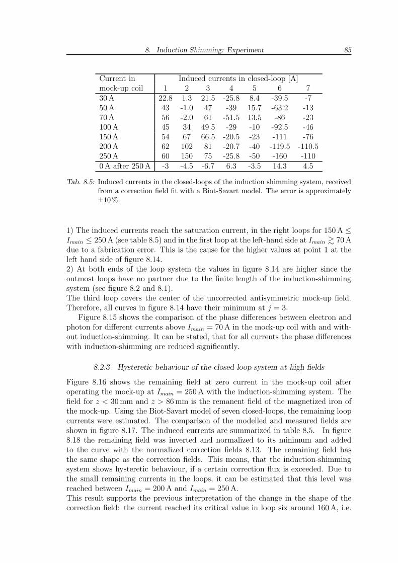
8. Induction Shimming: Experiment 85
Current in Induced currents in closed-loop [A]mock-up coil 1 2 3 4 5 6 730 A 22.8 1.3 21.5 -25.8 8.4 -39.5 -750 A 43 -1.0 47 -39 15.7 -63.2 -1370 A 56 -2.0 61 -51.5 13.5 -86 -23100 A 45 34 49.5 -29 -10 -92.5 -46150 A 54 67 66.5 -20.5 -23 -111 -76200 A 62 102 81 -20.7 -40 -119.5 -110.5250 A 60 150 75 -25.8 -50 -160 -1100 A after 250 A -3 -4.5 -6.7 6.3 -3.5 14.3 4.5
Tab. 8.5: Induced currents in the closed-loops of the induction shimming system, receivedfrom a correction field fit with a Biot-Savart model. The error is approximately±10%.
1) The induced currents reach the saturation current, in the right loops for 150 A ≤Imain ≤ 250 A (see table 8.5) and in the first loop at the left-hand side at Imain & 70 Adue to a fabrication error. This is the cause for the higher values at point 1 at theleft hand side of figure 8.14.2) At both ends of the loop system the values in figure 8.14 are higher since theoutmost loops have no partner due to the finite length of the induction-shimmingsystem (see figure 8.2 and 8.1).The third loop covers the center of the uncorrected antisymmetric mock-up field.Therefore, all curves in figure 8.14 have their minimum at j = 3.
Figure 8.15 shows the comparison of the phase differences between electron andphoton for different currents above Imain = 70 A in the mock-up coil with and with-out induction-shimming. It can be stated, that for all currents the phase differenceswith induction-shimming are reduced significantly.
8.2.3 Hysteretic behaviour of the closed loop system at high fields
Figure 8.16 shows the remaining field at zero current in the mock-up coil afteroperating the mock-up at Imain = 250 A with the induction-shimming system. Thefield for z < 30 mm and z > 86 mm is the remanent field of the magnetized iron ofthe mock-up. Using the Biot-Savart model of seven closed-loops, the remaining loopcurrents were estimated. The comparison of the modelled and measured fields areshown in figure 8.17. The induced currents are summarized in table 8.5. In figure8.18 the remaining field was inverted and normalized to its minimum and addedto the curve with the normalized correction fields 8.13. The remaining field hasthe same shape as the correction fields. This means, that the induction-shimmingsystem shows hysteretic behaviour, if a certain correction flux is exceeded. Due tothe small remaining currents in the loops, it can be estimated that this level wasreached between Imain = 200 A and Imain = 250 A.This result supports the previous interpretation of the change in the shape of thecorrection field: the current reached its critical value in loop six around 160 A, i.e.
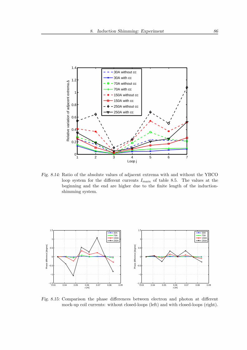
8. Induction Shimming: Experiment 86
1 2 3 4 5 6 70
0.2
0.4
0.6
0.8
1
1.2
1.4
Loop j
Rel
ativ
e va
riatio
n of
adj
acen
t ext
rem
a ∆
30A without cc
30A with cc
70A without cc
70A with cc
150A without cc
150A with cc
250A without cc
250A with cc
Fig. 8.14: Ratio of the absolute values of adjacent extrema with and without the YBCOloop system for the different currents Imain of table 8.5. The values at thebeginning and the end are higher due to the finite length of the induction-shimming system.
0.03 0.04 0.05 0.06 0.07 0.08 0.09−1.5
−1
−0.5
0
0.5
1
1.5
z [m]
Pha
se d
iffer
ence
[deg
ree]
30A70A150A250A
0.03 0.04 0.05 0.06 0.07 0.08 0.09−1.5
−1
−0.5
0
0.5
1
1.5
z [m]
Pha
se d
iffer
ence
[deg
ree]
30A70A150A250A
Fig. 8.15: Comparison the phase differences between electron and photon at differentmock-up coil currents: without closed-loops (left) and with closed-loops (right).
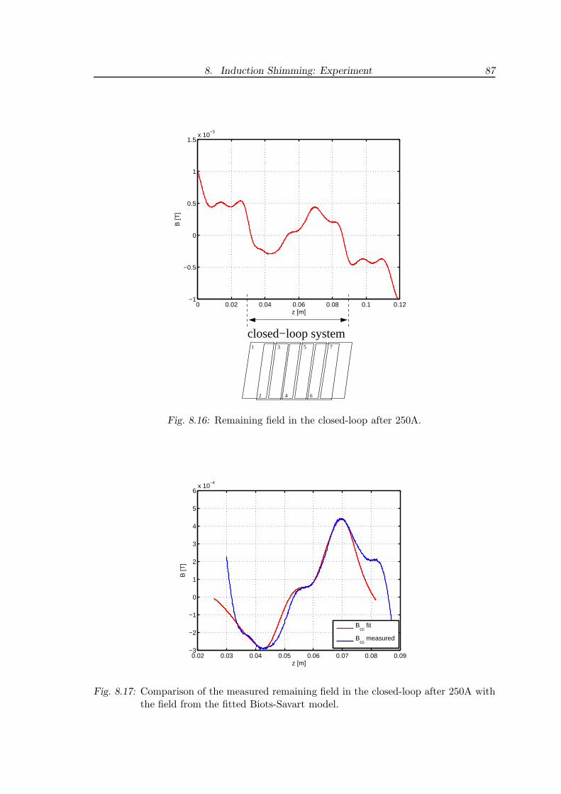
8. Induction Shimming: Experiment 87
1 3 5 7
2 64
0 0.02 0.04 0.06 0.08 0.1 0.12−1
−0.5
0
0.5
1
1.5x 10
−3
z [m]
B [T
]
closed−loop system
Fig. 8.16: Remaining field in the closed-loop after 250A.
0.02 0.03 0.04 0.05 0.06 0.07 0.08 0.09−3
−2
−1
0
1
2
3
4
5
6x 10
−4
z [m]
B [T
]
Bcc
fit
Bcc
measured
Fig. 8.17: Comparison of the measured remaining field in the closed-loop after 250A withthe field from the fitted Biots-Savart model.
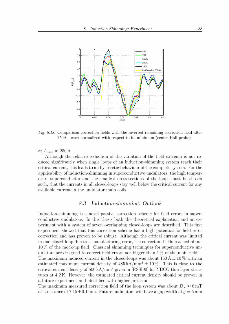
8. Induction Shimming: Experiment 88
0 0.02 0.04 0.06 0.08 0.1 0.12−1
−0.8
−0.6
−0.4
−0.2
0
0.2
0.4
0.6
0.8
1
z [m]
B/|B
min
|
30A
70A
150A
200A
250A
inv(0A after 250A)
Fig. 8.18: Comparison correction fields with the inverted remaining correction field after250A - each normalized with respect to its minimum (center Hall probe)
at Imain ≈ 250 A.Although the relative reduction of the variation of the field extrema is not re-
duced significantly when single loops of an induction-shimming system reach theircritical current, this leads to an hysteretic behaviour of the complete system. For theapplicability of induction-shimming in superconductive undulators, the high temper-ature superconductor and the smallest cross-sections of the loops must be chosensuch, that the currents in all closed-loops stay well below the critical current for anyavailable current in the undulator main coils.
8.3 Induction-shimming: Outlook
Induction-shimming is a novel passive correction scheme for field errors in super-conductive undulators. In this thesis both the theoretical explanation and an ex-periment with a system of seven overlapping closed-loops are described. This firstexperiment showed that this correction scheme has a high potential for field errorcorrection and has proven to be robust. Although the critical current was limitedin one closed-loop due to a manufacturing error, the correction fields reached about10 % of the mock-up field. Classical shimming techniques for superconductive un-dulators are designed to correct field errors not bigger than 1 % of the main field.The maximum induced current in the closed-loops was about 160 A± 10 % with anestimated maximum current density of 485 kA/mm2 ± 10 %. This is close to thecritical current density of 500 kA/mm2 given in [RSSI90] for YBCO thin layer struc-tures at 4.2 K. However, the estimated critical current density should be proven ina future experiment and identified with higher precision.The maximum measured correction field of the loop system was about Bcc ≈ 6 mTat a distance of 7.15±0.1 mm. Future undulators will have a gap width of g = 5 mm
8. Induction Shimming: Experiment 89
and roughly a field amplitude of B ≈ 1.5 T. Correction schemes are designed tocorrect at maximum field errors of 1 % of the main field, i.e. about ≈ 15 mT. Thedistance between the beam axis and the midplane of the induction-shimming systemwill be about g/2 = 2.5 mm. Due to Biot-Savart’s law the field behaves inverselyproportional to the distance: B ∼ 1
r. Therefore, the correction field at a distance
of 2.5 mm is Bcc,1 ≈ 17 mT. One induction-shimming system will be installed ateach undulator coil, the maximum correction field on the beam axis becomes thenBcc,2 ≈ 34 mT. This is already more than 2 % of the amplitude of the undulatorfield. Therefore, the induction-shimming test device fulfills the requirement.
A major issue for the applicability of induction-shimming is the reduction ofthe thickness of the substrate on which the YBCO layer is coated. The substrateused for this experiment had a thickness of 500 µm. Thus, the complete device hada thickness of 1 mm. Mounting such a system on both coils would either reducethe beam stay clear by about 2 mm or require an increase of the magnetic gap,which would reduce the magnetic field on axis. Therefore, the thickness of thestructure has to be reduced to an acceptable level. This can be achieved by usingthinner substrates and by structuring both sides of the substrate. With a substratethickness of 250 µm the gap would be increased only by 0.5 mm comparable withactive in-gap shimming concepts.Another possibility would be to create HTSC structures on the stainless steel liner,which will separate the superconductive coils from the beam in the future SCU15for ANKA, which is now under construction. This would totally avoid an additionalincrease of the magnetic gap.In the near future it is planned to integrate the loops in a 15 period SCU15 mock-upand to discuss afterwards the integration of an induction shimming concept in a fulllength 100 period undulator. There is no fundamental obstacle against scaling to fullundulator dimensions. If the system has to be assembled from shorter overlappingclosed-loop systems, their alignment is an important issue.
9. CONCLUSION
In this thesis a novel concept for reducing phase errors in superconductive undu-lators is described. Undulators in synchrotron light sources emit a line spectrumin the X-ray regime. The line width is determined mainly by the beam quality(emittance and energy spread of the electron beam) and the quality of the magneticfield. Small mechanical deviations from the design values and field distortions fromperiod to period can reduce the brilliance of the radiation and therefore have to becorrected.A measure for the global effect of distributed local field errors in the undulator isthe so-called phase error. A negligible small phase error means that the oscillatingelectron and the emitted light are always in phase along the trajectory in the un-dulator. Phase errors are caused by variations of the field strength and the periodlength from period to period.
These variations in superconductive undulators are basically due to mechanicaldeviations in the undulator coils. The effect of the different possible types of me-chanical inaccuracies - pole and wire bundle displacement with respect to the beamaxis and variation of the period length - was analyzed. It was shown that the dif-ferent field error contributions depend differently on the operation current of theundulator, due to the saturation behaviour of the iron poles. By an analyses of themeasured field of the SCU14 installed at ANKA it was shown that it is possible todistinguish field errors caused by a displacement of poles and wire bundles.The phase error of an undulator is determined not only by the amplitude of local fielderrors but also strongly depends on their distribution over the length of the device.In this work, the effect of statistically and systematically distributed mechanicalerrors on the phase error of superconductive undulators was examined using a sinewave model. For statistical error distributions the variation of the period lengthwas identified as the dominating contribution while the wire bundle variations havethe smallest effect on the phase error. In contrast, for systematic error distributionsthe phase error is dominated by displacements of the wire bundles. For systematicerrors the effects of neighbouring wire bundle on the extremum add up. In contrastto that for statistically distributed deviations there is a high probability that theeffects of neighbouring wire bundles cancel. It was shown that the phase error dueto systematic deviations is the smaller the shorter the correlation lengths of thedeformations are.
For the correction of field errors in superconductive undulators several schemesexist: mechanical shimming, shimming with integral correctors and active shimmingwith local correction coils. These classical concepts were discussed with respectto their advantages, disadvantages and limitations. A procedure for mechanicalshimming of superconductive undulators was described. Shimming with integral
9. Conclusion 91
correctors gives promissing results for the SCU14 installed at ANKA.The field of a single pole can in general only be changed by a current throughsuperconducting wires which are placed close to the pole. As the distance betweenwire and beam axis increase the field changes distribute over several poles when thematerial between the poles is magnetic. Using non-magnetic material between thepoles (the so-called laminated undulator), for instance copper, the correcting wirescan be further away, for instance at the side of the undulator (lateral shim coils).Nevertheless, shimming with actively powered coils is time consuming since theundulator has to be cooled down several times for measurements. In addition, theshim currents might be different for different undulator currents.
These complications stimulated the idea to think about a passive self-adaptiveshimming system which only depends on the field error and not on its source. Sucha novel passive shimming concept based on superconductive closed-loops - inductionshimming - was proposed in this thesis. In this method HTSC closed loops arepositioned on the surface of the undulator. The width of these loops is one or severalperiod lengths long in beam direction. In case of an ideal undulator the integral fluxis zero. With deviations from the ideal undulator (one pole has a different fieldthan the other) currents are induced in the loop which compensate automaticallythe error.The theory of induction shimming was derived from Faraday’s law of inductionand simulations with a Biot-Savart model showed that phase errors can be reducedsignificantly by this method. It was also shown, that the correction efficiency isquite robust against lateral and angular misalignment of the closed-loop system.The theoretical concept of induction-shimming was published in Physical ReviewSpecial Topics - Accelerators and Beams [WBP+08b] and a manuscript with theexperimental results was just submitted to the same journal [WBP+08a]. A patentfor this novel shimming method is pending [WBR08].In recently performed proof of principle experiments with a system of seven closedloops made from 330 nm thick YBCO layers the concept of induction shimming wassuccessfully demonstrated. The system reduced the variation of the field extrema,the first field integral, the second field integral and the phase difference betweenelectron and photon for the four periods covered by the closed-loops significantly.The critical current density reached in the test device was in good agreement withthe critical current densities published in literature for thin YBCO films at 4.2 K.The measured currents in the loops are high enough to shim a real undulator witha field error of up to 1 %. The next step is install a complete induction shimmingsystem in a SCU15 mock-up undulator with a length of 15 periods, now underconstruction.
Acknowledgements
The author thanks Prof. Dr.rer.nat. T. Baumbach from the Laboratory for Appli-cations of Synchrotron Radiation (LAS) and Prof. Dr.rer.nat G. Quast from theInstitute of Experimental Nuclear Physics at the University of Karlsruhe (TH) forsupport and advice.The author also wants to thank PD Dr. R. Rossmanith from the Institute for Syn-chrotron Radiation (ISS) at Forschungszentrum Karlsruhe and Dr. A. Bernhard(LAS) for the close collaboration, fruitful discussions, critical comments, opennessfor new ideas, scientific supervision and their friendship.The research work for this thesis was performed at LAS in close collaboration withthe Institute for Synchrotron Radiation (ISS), also headed by Prof. Dr.rer.nat. T.Baumbach, at the Forschungszentrum Karlsruhe. Therefore, the author wants tothank all colleagues from ISS for their hospitality and support.The author wants to thank especially the members of the three groups at LAS, ISSand the University of Erlangen-Nurnberg which closely collaborate i on the devel-opment of superconductive undulators: Dr. S. Casalbuoni (ISS), Dr. A. W. Grau(ISS), Dr. B. Kostka (University of Erlangen-Nurnberg), Dr. E. Mashkina (Univer-sity of Erlangen-Nurnberg), Dr. D. Saez de Jauregui (ISS), Dr. P. Peiffer (LAS)and N. Vassiljev (University of Erlangen-Nurnberg) for their support.The author also wants to thank the ANKA/ISS machine group for good collabora-tion and support, especially Dr. I. Birkel, Dr. E. Huttel and Dr. P. Wesolowski.Special thanks goes to Dr. A.-S. Muller (ISS/LAS) for advice, support, scientificdiscussions and especially her friendship.Over the past three years several students have contributed to the research work pre-sented in this thesis. Therefore, the author wants to thank the students F. Burkart,S. Ehlers, G. Fuchert, D. Schorling and M.J. Wolf for their participation in dataanalyses and experiments and the excellent team work.The author also wants to thank the colleagues from LAS: Dr. K. Eichhorn, M. Fis-cher, Dr. D. Grygoryev, Dr. I. Huber, M. Riotte, Dr. K. Sonnad, T. Ulyanenkovaand Prof. emerit. Dr. H. Wondratschek for their support.Special thanks goes to D. Erbe (ISS) and the workshop of the Institute for PhysicsII at the University of Erlangen (Prof. Dr.rer.nat. E. Steffens) for designing, fabri-cating and mounting the essential parts of the equipment for the performed proofof principal experiment on induction shimming.The mock-up coil used in the experiment was built by Babcock Noell GmbH (BNG),Wurzburg, Germany. The author wants to thank the colleagues Dr. C. Boffo, M.Borlein and Dr. W. Walter from BNG for their collaboration.The induction shimming test device was produced by the company THEVA, Isman-ing, Germany. The author wants to thank Dr. R. Semerad and Dr. W. Prusseitfrom THEVA for their openess, flexibility and the excellent collaboration.Finally the author wants to thank his family, the friends from the SMD Karlsruheand the Jesus-Bruderschaft Gnadenthal, the members of the music-team of the Lau-rentiuspfarrei Karlsruhe-Hagsfeld and of the Waldstadt Kammerorchester Karlsruhe,S. Rauh and M. Swoboda for their sustaining friendship, support, tolerance and pa-tience over the past years.
BIBLIOGRAPHY
[ABB+80] A. S. Artamonov, L. M. Barkov, V. B. Baryshev, N. S. Bashtonoy,N. A. Vinokurov, E. S. Gluskin, G. A. Korniukhin, V. A. Kochubei,G. N. Kulipanov, N. A. Mezentsev, V. F. Pindiurin, A. N. Skrinsky,and V. M. Khorev. First results of the work with a superconducting“snake” at the VEPP-3 storage ring. Nuclear Instruments and Methods,177:239–246, 1980.
[BCS57] J. Bardeen, L. N. Cooper, and J. R. Schrieffer. Theory of superconduc-tivity. Physical Review, 108(5):1175, December 1957.
[Ber] A. Bernhard. private communication.
[Ber08] Axel Bernhard. Laminierter supraleitender Undulator. Erfind-ungsmeldung, August 2008.
[BHK+06] A. Bernhard, M. Hagelstein, B. Kostka, R. Rossmanith, T. Schneider,M. Weisser, D. Wollmann, T. Baumbach, E. Steffens, and G. Gerlach.Superconductive in-vacuum undulators. IEEE Transactions on Applied
Superconductivity, 16(2):1228–1231, 2006.
[BK04a] Werner Buckel and Reinhold Kleiner. Superconductivity, chapter Intro-duction, pages 1–9. Wiley-VCH, 2004.
[BK04b] Werner Buckel and Reinhold Kleiner. Superconductivity, chapter Ther-modynamics and Thermal Properties of the Superconducting State,pages 189–267. Wiley-VCH, 2004.
[BK04c] Werner Buckel and Reinhold Kleiner. Superconductivity, chapter Crit-ical Currents in Type-I and Type-II Superconductors, pages 269–304.Wiley-VCH, 2004.
[BK04d] Werner Buckel and Reinhold Kleiner. Superconductivity, chapter Super-conducting Elements, Alloys, and Compounds, pages 73–109. Wiley-VCH, 2004.
[BK04e] Werner Buckel and Reinhold Kleiner. Superconductivity, chapter Fun-damental Properties of Superconductors, pages 11–71. Wiley-VCH,2004.
[BKP+] A. Bernhard, B. Kostka, P. Peiffer, R. Rossmanith, D. Schoerling, M.J.Wolf, D. Wollmann, and T. Baumbach. Magnetic Field Analysis for the
Bibliography 94
ANKA Superconductive Undulator. Nuclear Instruments and Methods
in Physics Research A. to be published.
[BM86] J. G. Bednorz and K. A. Mueller. Possible high Tc superconductivityin the Ba-La-Cu-O system. Zeitschrift fuer Physik B, 64:189, 1986.
[BPW08] Axel Bernhard, Peter Peiffer, and Daniel Wollmann. Shimming-Konzeptionen fuer die Projekte SCUW/SCU2. internal report, June2008.
[BSMM01] I.N. Bronstein, K.A. Semendjajew, G. Musiol, and H. Muehlig.Taschenbuch der Mathematik, chapter Unbestimmte Integrale, page1053. Verlag Harri Deutsch, 5th edition, 2001.
[BY01] C. Buzea and T. Yamashita. Review of the superconducting propertiesof MgB2. Superconductor Science and Technology, 14:R115, 2001.
[BZJIW90] I. Ben-Zvi, Z.Y. Jiang, G. Ingold, and L.H. Wu. The performance of asuperconductive micro-undulator prototype. Nuclear Instruments and
Methods in Physics Research A, 297:301, 1990.
[CEC97] O. Chubar, P. Elleaume, and J. Chavanne. A 3D Magnetostatics Com-puter Code for Insertion Devices. Proceedings of the SRI97 Conference,
SPring8, Japan, 1997.
[CHK+06] S. Casalbuoni, M. Hagelstein, B. Kostka, R. Rossmanith, M. Weisser,E. Steffens, A. Bernhard, D. Wollmann, and T. Baumbach. Generationof x-ray radiation in a storage ring by a superconductive cold-bore in-vacuum undulator. Physical Review Special Topics Accelerators and
Beams, 9:010702, 2006.
[Cla04a] J.A. Clarke. The Science and Technology of Undulators and Wigglers,chapter Synchrotron Radiation Output from Undulators, pages 52–83.Oxford Science Publication, 2004.
[Cla04b] J.A. Clarke. The Science and Technology of Undulators and Wigglers,chapter Measurement and Correction of Insertion Devices, pages 158–179. Oxford Science Publication, 2004.
[CRS+03] S. Chouhan, R. Rossmanith, S. Strohmer, D. Doelling, A. Geisler,A. Hobl, and S. Kubsky. Field error compensation and thermal beamload in a supercondictive undulator. Proceedings of the 2003 Partical
Accelerator Conference, pages 899–901, 2003.
[ECC97] P. Elleaume, O. Chubar, and J. Chavanne. Computing 3D MagneticFields from Insertion Devices. Proceedings of the 1997 Partical Accel-
erator Conference, Vancouver, 1997.
[Ell03] Pascal Elleaume, editor. Workshop on superconducting Wigglers and
Undulators. ESRF, 2003.
Bibliography 95
[Far80] Y. Farge. Emission of photons by undulators. Applied Optics, 19:4021,1980.
[HHM+99] T. Hezel, M. Homscheidt, H.O. Moser, R. Rossmanith, T. Schneider,H. Backe, S. Dambach, F. Hagenbuck, K.H. Kaiser, G. Kube, W. Lauth,A. Steinhof, and T. Walcher. Experimental results with a novel su-perconductive in-vacuum mini-undulator test device at the Mainz mi-crotron MAMI. Proceedings of the 1999 Particle Accelerator Confer-
ence, (165-167), 1999.
[Hof04] Albert Hofmann. The Physics of Synchrotron Radiation. CambridgeUniversity Press, first edition, 2004.
[IOR+98] T. Ishida, Kiichi Okuda, A. I. Rykov, S. Tajima, and I. Terasaki. In-plane anisotropy of vortex-lattice melting in large YBa2Cu3O7 singlecrystals. Physical Reviwe B, 58(9):5222, 1998.
[Jac99a] J. D. Jackson. Classical Electrodynamics. John Wiley & Sons, Inc.,third edition, 1999.
[Jac99b] J. D. Jackson. Classical Electrodynamics, chapter Magnetostatics, Fara-day’s Law, Quasi-Static Fields, pages 175–178. John Wiley & Sons,Inc., third edition, 1999.
[KO11] H. Kammerlingh-Onnes. Comm. Leiden, 1911.
[KRH+05] B. Kostka, R. Rossmanith, M. Hagelstein, T. Baumbach, A. Bernhard,M. Weisser, and E. Steffens. Generation of X-Ray radiation in a storagering by a superconductive cold-bore in-vacuum undulator. Physical
Review Letters, submitted, 2005.
[KSW91] Koch, Sasaki, and Winick. Handbook on Synchrotron Radiation, vol-ume 3, chapter Synchrotron-radiation spectra, section Radiation fromundulator magnets, pages 43–52. North-Holland, 1991.
[KSW00] Kories and Schmidt-Walter. Taschenbuch der Elektrotechnik, chapterElektrische Felder, pages 88–89. Verlag Harri Deutsch, 2000.
[KT96] J. R. Kirtley and C. C. Tsuei. Spektrum der Wissenschaft, page 58,October 1996. German edition of Scientific American.
[Lab] Stanford Synchrotron Radiation Laboratory. http://www-ssrl.slac.stanford.edu/sr sources.html.
[MD04] H.O. Moser and C.Z. Diao. Finite-Length field error and its compen-sation in superconducting miniundulators. Nuclear Instruments and
Methods, Section A, (535):606–613, June 2004.
Bibliography 96
[MGS+08] Elena Mashkina, Andreas Grau, Theo Schneider, Axel Bernhard, SaraCasalbuoni, Michael Hagelstein, Barbara Kostka, Robert Rossmanith,Erhard Steffens, Daniel Wollmann, and Tilo Baumbach. CASPER - amagnetic measurement facility for superconducting undulators. Journal
of Physics: Conference Series, 97, 2008.
[MKH91] H.O. Moser, B. Krevet, and H. Holzapfel. Mikroundulator. Germ patent
P 41 01 094.9-33, Jan. 16 1991.
[MO33] W. Meissner and R. Ochsenfeld. Ein neuer Effekt bei Eintritt derSupraleitfaehigkeit. Die Naturwissenschaften, 21:787, 1933.
[Mos04] H.O. Moser. Accelerator Physics, Technology, and Applications, chapterA Guided Survey of Synchrotron Radiation Sources. Singapore, WorldScientific Publishing, 2004.
[Mue05] A.-S. Mueller. Physik relativistischer Teilchenstrahlen. Lecture at theUniversity of Siegen, SS 2005.
[MWY04] H.O. Moser, O. Wilhelmi, and P. Yang. Accelerator Physics, Technol-
ogy, and Applications, chapter Introduction to Synchrotron RadiationApplications. Singapore, World Scientific Publishing, 2004.
[NNMZ01] J. Nagamatsu, N. Nakagawa, T. Muranaka, and Y. Zenitani. Nature,410:63, 2001.
[NTME98] H. Nakagawa, T. Takamasu, N. Miura, and Y. Enomoto. DC and ACmagneto-resistance measurement technique forYBa2Cu3O7−δ thin filmsin megagauss fields. Physica B, 246:429, 1998.
[OE03] H. Onuki and P. Elleaume, editors. Undulators, Wigglers and their
Applications, volume 1, chapter Technology of insertion devices, pages148–213. Taylor & Francis, 2003.
[PDB+05] S. Prestemon, D. Dietderich, S. Bartlett, M. Coleman, S. Gourlay,A. Lietzke, S. Marks, S. Mattafirri, R. Scanlan, R. Schlueter, B. Wahrer,and B. Wang. Design, Fabrication, and Test Results of Undulators Us-ing Nb3Sn Superconductor. IEEE Transactions on Applied Supercon-
ductivity, 15(2):1236–1239, June 2005.
[Pfl05] J. Pflueger. Undulator systems for the X-FEL. International Work-
shop on Undulator Systems for Free Electron Lasers, DESY, Hamburg,
Germany, 2005.
[PLT99] J. Pflueger, H. Lu, and T. Teichmann. Field fine tune by pole heightadjustment for undulator of the TTF-FEL. Nuclear Instruments &
Methods in Physic Research, A429:368–391, 1999.
Bibliography 97
[PWBF08] Peter Peiffer, Daniel Wollmann, Axel Bernhard, and Golo Fuchert.Phase errors from systematic distributions of mechanical errors. in-ternal report, Oktober 2008.
[RMG+02] R. Rossmanith, H.O. Moser, A. Geisler, A. Hobl, D. Krischel, andM. Schillo. Superconductive 14 mm period undulators for single passaccelerators (fels) and storage rings. Proceedings of EPAC 2002, (2628-2630), 2002.
[RSSI90] B. Roas, L. Schultz, and G. Saemann-Ischenko. Anisotropy of the crit-ical current density in epitaxial Y Ba2Cu3Ox films. Physical Review
Letters, 64(4):479–482, 1990.
[Sak67] J. J. Sakurai. Advanced Quantum Mechanics, chapter Classical Fields,pages 1–19. Addison-Wesley Publishing Company, 1967.
[TK] T. Tanaka and H. Kitamura. SPring-8/RIKEN.http://radiant.harima.riken.go.jp/spectra.
[Vac01] Vacuumschmelze. Weichmagnetische Kobalt-Eisen-Legierungen.http://www.vacuumschmelze.de//dynamic/docroot/medialib/documents/broschueren/htbrosch/Pht-004 d.pdf, 2001.
[VF] UK Vector Fields, Oxford. OPERA-3D.
[WBC+06] Daniel Wollmann, Axel Bernhard, Sara Casalbuoni, Michael Hagel-stein, Barbara Kostka, Robert Rossmanith, Matthias Weisser, ErhardSteffens, Gerald Gerlach, and Tilo Baumbach. A concept on electricfield error compensation for the ANKA superconducting undulator.In Proceedings of EPAC 2006, Edinburgh, Scotland, pages 3577–3579,2006.
[WBP+08a] D. Wollmann, A. Bernhard, P. Peiffer, T. Baumbach, E. Mashkina,A. Grau, and R. Rossmanith. Experimental Demonstration of theInduction-Shimming Concept in Superconductive Undulators. Phys-
ical Review Special Topics Accelerators and Beams, 2008. submitted.
[WBP+08b] D. Wollmann, A. Bernhard, P. Peiffer, T. Baumbach, and R. Ross-manith. Induction-Shimming: a new shimming-concept for supercon-ductive undulators. Physical Review Special Topics Accelerators and
Beams, 11:100702, 2008.
[WBP+08c] D. Wollmann, A. Bernhard, P. Peiffer, R. Rossmanith, and T. Baum-bach. A new concept for reducing phase errors in superconductiveundulators: induction-shimming. In Proceedings of EPAC08, Genoa,
Italy, pages 2323–2325, 2008.
[WBR08] D. Wollmann, A. Bernhard, and R. Rossmanith. Induction shimming.German patent, June 2008. pending.
Bibliography 98
[Wie03a] Helmut Wiedemann. Particle Accelerator Physics I, chapter Syn-chrotron Radiation, pages 300–336. Springer, second edition, 2003.
[Wie03b] Helmut Wiedemann. Particle Accelerator Physics I. Springer, secondedition, 2003.
[Wie03c] Helmut Wiedemann. Particle Accelerator Physics II. Springer, secondedition, 2003.
[Wil] Klaus Wille. Vorlesung zur Physik der Teilchenbeschleuniger. Lectureat the University of Dortmund.
[Wil92a] Klaus Wille. Physik der Teilchenbeschleuniger, chapter Synchrotron-strahlung, pages 36–49. B. G. Teubner Stuttgart, 1992.
[Wil92b] Klaus Wille. Physik der Teilchenbeschleuniger. B. G. TeubnerStuttgart, 1992.
[Wil92c] Klaus Wille. Physik der Teilchenbeschleuniger und Synchrotron-
strahlungsquellen, chapter Wiggler und Undulatoren, pages 249–266.Teubner Stuttgart, 1992.
[Wol05] Daniel Wollmann. Reduktion des Phasenfehlers eines SupraleitendenUndulators. Master’s thesis, Technische Universitaet Dresden, Ger-many, 2005.
[Zha02] X.-C. Zhang. Terahertz wave imaging: horizons and hurdles. Physics
in Medicine and Biology, 47:3667–3677, 2002.
LIST OF FIGURES
2.1 Angular distribution of the electro-magnetic radiation emitted by atransversely accelerated relativistic charged particle. . . . . . . . . . . 8
2.2 Synchrotron radiation spectrum of the ANKA bending magnets. . . . 82.3 The three main sources for synchrotron radiation: bending magnet
(top), wiggler (center), undulator (bottom). . . . . . . . . . . . . . . 92.4 Comparison of the calculated radiation spectra emitted by an ANKA
bending magnet, an ANKA wiggler and the ANKA SCU14. . . . . . 102.5 Principle layout of a superconductive undulator. . . . . . . . . . . . . 112.6 Schematic drawing of a permanent-magnet undulator. . . . . . . . . . 112.7 Maximum achievable field strength for different undulator types. . . . 122.8 Trajectory of an electron passing through the magnetic field of an
undulator. . . . . . . . . . . . . . . . . . . . . . . . . . . . . . . . . . 142.9 Simulated undulator spectrum for a 100 period undulator. . . . . . . 152.10 Measured spectrum of the SCU14 installed at ANKA. . . . . . . . . . 162.11 Tuning curves of the SCU14 installed at ANKA. . . . . . . . . . . . . 162.12 Correlation between the motion of the electron and the emitted light 17
3.1 Principle layout of a superconductive undulator. . . . . . . . . . . . . 203.2 Cut of a superconductive undulator with deviation of pole height and
wire bundle position. . . . . . . . . . . . . . . . . . . . . . . . . . . . 203.3 Field error caused by variation of a pole position. . . . . . . . . . . . 213.4 Disturbance of the net electron trajectory and phase difference - pole
position variation. . . . . . . . . . . . . . . . . . . . . . . . . . . . . . 223.5 Field error caused by variation of a wire bundle position. . . . . . . . 223.6 Disturbed net electron trajectory and phase difference - variation of
wire bundle position. . . . . . . . . . . . . . . . . . . . . . . . . . . . 233.7 Field error caused by variation of the period length. . . . . . . . . . . 243.8 Disturbed net electron trajectory and phase difference - variation the
period length. . . . . . . . . . . . . . . . . . . . . . . . . . . . . . . . 243.9 B versus current. . . . . . . . . . . . . . . . . . . . . . . . . . . . . . 253.10 Difference between ideal and disturbed fields versus current. . . . . . 263.11 SCU14 raw field. . . . . . . . . . . . . . . . . . . . . . . . . . . . . . 283.12 SCU14 field decomposition . . . . . . . . . . . . . . . . . . . . . . . . 28
4.1 Relative field change caused by a variation of the pole position againstthe beam axis. . . . . . . . . . . . . . . . . . . . . . . . . . . . . . . . 30
4.2 Relative field change caused by a variation of the wire bundle positionagainst the beam axis. . . . . . . . . . . . . . . . . . . . . . . . . . . 31
List of Figures 100
4.3 Monte-Carlo simulations: variation of the pole (left) and wire bundlepositions (right). . . . . . . . . . . . . . . . . . . . . . . . . . . . . . 32
4.4 Monte-Carlo simulation: variations of the half period lengths andcombination of all three types of mechanical deviations. . . . . . . . . 33
4.5 Linear and seesaw deformation of the poles. . . . . . . . . . . . . . . 344.6 Parabolic deformations of the pole positions. . . . . . . . . . . . . . . 344.7 Sinusoidal deformations of the pole positions. . . . . . . . . . . . . . 344.8 Rectangular deformations of the pole positions. . . . . . . . . . . . . 35
5.1 Mechanical shimming concept for the XFEL undulator systems. . . . 375.2 Sketch of the integral correctors placed in the SCU14. . . . . . . . . . 385.3 Magnetic field of the SCU14 at 900A. . . . . . . . . . . . . . . . . . . 395.4 Comparison of the first (left) and second field integral (right) of the
SCU14 with and without integral shimming. . . . . . . . . . . . . . . 405.5 Model of a superconductive undulator with additional in gap shim coils. 415.6 Pole slice of a superconductive undulator model with in gap shim coils. 425.7 Correction fields caused by air-core in gap shimming coils and in gap
shimming coils mounted on complete unsaturated coil bodys. . . . . . 435.8 Scetch with in iron shimming coils. . . . . . . . . . . . . . . . . . . . 445.9 Correction fields caused by air-core in iron shimming coils and in iron
shimming coils mounted in complete unsaturated coil bodys. . . . . . 455.10 Model of a superconductive undulator with lateral shimming coils. . . 465.11 Correction fields caused by air-core lateral shimming coils and lateral
shimming coils mounted on complete unsaturated coil bodys. . . . . . 465.12 Principle layout of a superconductive undulator. . . . . . . . . . . . . 475.13 Correction fields caused by air-core lateral shimming coils and lateral
shimming coils mounted on a laminated undulator with unsaturatedpole discs. . . . . . . . . . . . . . . . . . . . . . . . . . . . . . . . . . 47
6.1 Superconductivity of mercury. . . . . . . . . . . . . . . . . . . . . . . 496.2 Evolution of the superconducting transition temperatures. . . . . . . 506.3 Sketch of the expulsion of an external magnetic field by a supercon-
ducting sphere. . . . . . . . . . . . . . . . . . . . . . . . . . . . . . . 516.4 Critical magnetic field plotted versus the temperature for different
type-I superconductors. . . . . . . . . . . . . . . . . . . . . . . . . . . 526.5 Average magnetic field in the interior of a type-II superconductor
plotted against the external magnetic field. . . . . . . . . . . . . . . . 536.6 Schematical phase diagram of a type-II superconductor. . . . . . . . . 546.7 Crystal structure of MgB2 [BY01] (left) and YBa2Cu3O7 [BK04d]
(right). . . . . . . . . . . . . . . . . . . . . . . . . . . . . . . . . . . . 556.8 Schematic drawing of a superconductor in the Shubnikov phase with
magentic flux lines and shielding currents. . . . . . . . . . . . . . . . 566.9 Critical current density of a YBCO thin film for three temperatures
plotted versus the external magnetic field. . . . . . . . . . . . . . . . 57
List of Figures 101
7.1 Influence of a closed loop on a one period rectangular magnetic fieldwith different magnetic flux densities in each half period. . . . . . . . 60
7.2 Behaviour of two overlapping closed-loops in a rectangular magneticfield with different field amplitudes. . . . . . . . . . . . . . . . . . . . 61
7.3 Rectangular field with n+1 half periods and n overlapping closed loops 617.4 Cross section of an undulator with the main coils (green: iron; red:
superconductive wire-bundles) and overlapping closed-loops for cor-rection (magenta) placed close to the main coils. . . . . . . . . . . . . 64
7.5 One closed-loop made out of two long straight wires . . . . . . . . . . 647.6 Two overlapping closed-loops with induced currents I1 and I2. . . . . 657.7 Comparison of the magnetic field along the beam axis with (black)
and without (red) induction shimming. . . . . . . . . . . . . . . . . . 677.8 Comparison of the first/second field integral along the beam axis with
(blue/black) and without (red/red) induction shimming. . . . . . . . 677.9 Comparison of the first field integral along the beam axis with (blue)
and without (red) induction shimming extended by ten periods oneach side. . . . . . . . . . . . . . . . . . . . . . . . . . . . . . . . . . 68
7.10 Phase-error distribution for 1000 50-period undulators without (left)and with (right) induction-shimming; σ∆B
B,coil = σ∆B
B,pole = 3 · 10−3 . 69
7.11 Phase-error distribution for 1000 50-period undulators with a induction-shimming system misaligned by 0.5 mm against the zero crossings ofthe undulator main field; σ∆B
B,coil = σ∆B
B,pole = 3 · 10−3 . . . . . . . . 69
8.1 Photograph of the induction-shimming test device with seven over-lapping closed loops. . . . . . . . . . . . . . . . . . . . . . . . . . . . 72
8.2 Cut through the stacked induction-shimming structure with the sub-strate. . . . . . . . . . . . . . . . . . . . . . . . . . . . . . . . . . . . 72
8.3 Picture of the measurement setup. . . . . . . . . . . . . . . . . . . . . 738.4 Photograph of the experimental setup before installation in the cryostat. 748.5 Magnetic field from raw data at 350 A in the mock-up coil. The read
arrows mark the first and the last extremum of the field, which aresignificantly higher. This is due to the magnetization of the ironblocks at the beginning and the end of the undulator. . . . . . . . . . 76
8.6 Raw data of the field measurements at zero current (Hall probe 2) inthe mock-up coil before the measurement with the shimming equip-ment (red) and without (blue). . . . . . . . . . . . . . . . . . . . . . 76
8.7 Magnetization of the mock-up coil at the beginning of the measure-ment with the shimming equipment (red) and without (blue). . . . . 77
8.8 Comparison of corrected and uncorrected field and correction field -70A. . . . . . . . . . . . . . . . . . . . . . . . . . . . . . . . . . . . . 78
8.9 Fit of 7 closed-loop Biot-Savart model to correction field - current inmain coil: 70A . . . . . . . . . . . . . . . . . . . . . . . . . . . . . . 79
8.10 Phase differences between electron and photon at 70 A with and with-out correction coils (cc) . . . . . . . . . . . . . . . . . . . . . . . . . . 80
8.11 Comparison of first and second field integrals. . . . . . . . . . . . . . 808.12 Comparison of corrected field for different currents. . . . . . . . . . . 82

List of Figures 102
8.13 Comparison of the correction fields for different currents in the mock-up coil. The absolute fields (top) and the correction fields, each nor-malized with respect to its minimum (bottom) are shown. . . . . . . 84
8.14 Ratio of the absolute values of adjacent extrema with and withoutthe YBCO loop system for the different currents. . . . . . . . . . . . 86
8.15 Comparison of the phase differences at different mock-up coil currents. 868.16 Remaining field in the closed-loop after 250A. . . . . . . . . . . . . . 878.17 Comparison of the measured remaining field in the closed-loop after
250A with the field from the fitted Biots-Savart model. . . . . . . . . 878.18 Comparison correction fields with the inverted remaining correction
field after 250A - each normalized with respect to its minimum (centerHall probe) . . . . . . . . . . . . . . . . . . . . . . . . . . . . . . . . 88
B.1 Vacoflux BH curve. . . . . . . . . . . . . . . . . . . . . . . . . . . . . 109
LIST OF TABLES
2.1 Technical parameters of the electron storage ring ANKA. . . . . . . . 7
4.1 Design parameters for the magnetic field of the SCU15 presently un-der construction. . . . . . . . . . . . . . . . . . . . . . . . . . . . . . 29
4.2 Parameters used in the Opera-3D model for the SCU15. . . . . . . . 304.3 Comparison of the confidence levels of the phase error distributions
with normally distributed variations. . . . . . . . . . . . . . . . . . . 334.4 Comparison of phase errors caused by systematic deformations. . . . 35
5.1 Position of the centers of the corrector magnets relative to the centerof the SCU14 and their length. . . . . . . . . . . . . . . . . . . . . . 38
5.2 Comparison of phase errors before and after correction with the threeintegral correctors. . . . . . . . . . . . . . . . . . . . . . . . . . . . . 40
5.3 Fields in the corrector magnets for different phase error optimizations. 40
6.1 Overview of the transition temperatures and the critical magneticfield strengths for some superconducting elements. . . . . . . . . . . . 52
6.2 Overview of the transition temperatures and the critical magneticfield strengths for some type-II superconductors. . . . . . . . . . . . . 54
7.1 Comparison of the confidence-levels in the phase-error distributions. . 70
8.1 Offsets caused by Hall probes . . . . . . . . . . . . . . . . . . . . . . 758.2 Calculated induced currents for 70A . . . . . . . . . . . . . . . . . . . 798.3 Relative variation of minima and maxima. . . . . . . . . . . . . . . . 818.4 Relative variation between 4th and 5th minimum and 4th and 5th
maximum. . . . . . . . . . . . . . . . . . . . . . . . . . . . . . . . . . 838.5 Calculated induced currents . . . . . . . . . . . . . . . . . . . . . . . 85
B.1 Vacoflux50 BH data. . . . . . . . . . . . . . . . . . . . . . . . . . . . 109

APPENDIX
A. PHASE ERROR DERIVATION
The phase error can be derived from the equations of motion, as discussed in section2.2 [Wil].From the magnetic field of the undulator
B =
0By(z)
0
with By(z) = Bcos( 2πλu
z), and the Lorentz-force
F = meγv = −ev × B,
the equation of motion for the electron is
x0z
= −e
meγ
−z · By
0−x · By
.
Integration of
x =e
meγBy
dz
dt,
leads to
x =
t∫
t0
x · dt′ =e
meγ
z∫
z0
By(z′)dz′ =
e
meγI1(z), (A.1)
for x(t0) = 0. I1(z) is a periodic function in z.The relativistic factor γ is
γ =
√
√
√
√
1
1 −(
|v|c
)2 .
With |v|2 = x2 + z2 and 1γ2 ≪ 1
z =
√
c2
(
1 −1
γ2−
x2
c2
)
=
√
√
√
√c2
(
1 −1
γ2−
[
e
mecγI1(z)
]2)
≈ c
√
√
√
√
(
1 −
[
e
mecγI1(z)
]2)
. (A.2)
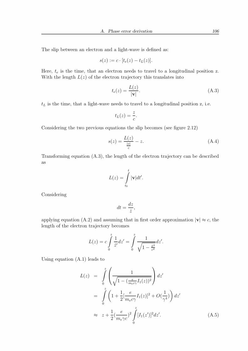
A. Phase error derivation 106
The slip between an electron and a light-wave is defined as:
s(z) := c · [te(z) − tL(z)].
Here, te is the time, that an electron needs to travel to a longitudinal position z.With the length L(z) of the electron trajectory this translates into
te(z) =L(z)
|v|. (A.3)
tL is the time, that a light-wave needs to travel to a longitudinal position z, i.e.
tL(z) =z
c.
Considering the two previous equations the slip becomes (see figure 2.12)
s(z) =L(z)|v|c
− z. (A.4)
Transforming equation (A.3), the length of the electron trajectory can be describedas
L(z) =
t∫
t0
|v|dt′.
Considering
dt =dz
z,
applying equation (A.2) and assuming that in first order approximation |v| ≈ c, thelength of the electron trajectory becomes
L(z) = c
z∫
0
1
z′dz′ =
z∫
0
1√
1 − x2
c2
dz′.
Using equation (A.1) leads to
L(z) =
z∫
0
1√
1 − ( emecγ
I1(z))2
dz′
=
z∫
0
(
1 +1
2[
e
mecγI1(z)]2 + O(
1
γ4)
)
dz′
≈ z +1
2(
e
meγc)2
z∫
0
[I1(z′)]2dz′. (A.5)
A. Phase error derivation 107
With J(z) =z∫
0
[I1(z′)]2dz′ and applying equation (A.5) to equation (A.4) the slip
between an electron and a light-wave becomes
s(z) =z + 1
2( e
mecγ)2J(z)
|v|c
− z
=z + 1
2( e
mecγ)2J(z)
|v|c
−z |v|
c|v|c
=z(1 − |v|
c) + 1
2( e
mecγ)2J(z)
|v|c
.
Assuming
γ2 =1
1 −(
|v|c
)2
→1
γ2= 1 −
(
|v|
c
)2
= (1 −|v|
c)(1 +
|v|
c)
the slip can be rewritten as
s(z) =
z(1−|v|c
)(1+|v|c
)
(1+|v|c
)+ 1
2( e
mecγ)2J(z)
|v|c
=
z
γ2(1+ |v|c
)+ 1
2( e
mecγ)2J(z)
|v|c
.
Applying |v| ≈ c yields
s(z) =z
2γ2+
1
2(
e
mecγ)2J(z)
=1
2γ2
(
z + (e
mec)2J(z)
)
(A.6)
The phase difference between photon and electron Φ(z), in radians is defined as thedifference between s(z) in units of the light wavelength λL and the z in units of theundulator period length λu:
Φ(z) := 2π
(
s(z)
λL
−z
λu
)
.
Applying equation (2.10) with k = 1 and Θ = 0:
λL =λu
2γ2(1 +
K2
2),
A. Phase error derivation 108
and equation (A.6) the phase difference between photon and electron becomes
Φ(z) = 2π
12γ2
(
z + ( emec
)2J(z))
λu
2γ2 (1 + K2
2)
−z
λu
=2π
λu
2(
z + ( emec
)2J(z))
− z(2 + K2)
2 + K2
=2π
λu
(
2( emec
)2J(z) − K2z)
2 + K2
)
.
Finally, to achieve equation (2.11), which is the phase difference between photonand electron for the half period i of an undulator with n periods, the substitutionz = zi − z0, with i = (1...2n) leads to
Φi =2π
λu
(
2( emec
)2J(zi − z0) − (zi − z0)K2
2 + K2
)
.
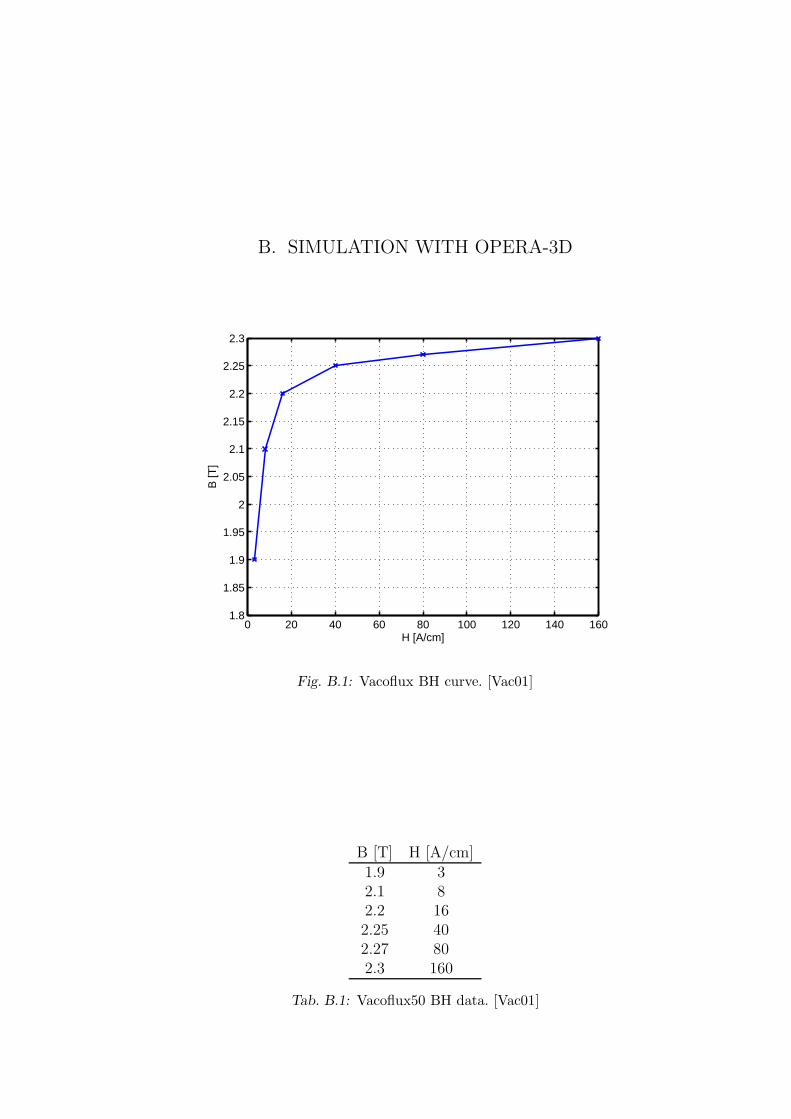
B. SIMULATION WITH OPERA-3D
0 20 40 60 80 100 120 140 1601.8
1.85
1.9
1.95
2
2.05
2.1
2.15
2.2
2.25
2.3
H [A/cm]
B [T
]
Fig. B.1: Vacoflux BH curve. [Vac01]
B [T] H [A/cm]1.9 32.1 82.2 162.25 402.27 802.3 160
Tab. B.1: Vacoflux50 BH data. [Vac01]