Embed Size (px)
Citation preview

International Journal of Emerging Engineering Research and Technology
Volume 3, Issue 8, August 2015, PP 96-109
ISSN 2349-4395 (Print) & ISSN 2349-4409 (Online)
*Address for correspondence:
International Journal of Emerging Engineering Research and Technology V3 ● I8 ● August 2015 96
A Novel Approach to Solve Deadlock Problem in On-Chip BUS
Communication
Vinola Purantra1, S.Subbanna
2, D.Subba Rao
3
1M.Tech, VLSI DESIGN SYSTEM, Siddhartha Institute of Engineering and Technology, Hyderabad,
TS, India 2Associate Professor, Dept of E.C.E, Siddhartha Institute of Engineering and Technology, Hyderabad, TS,India
3HOD, Dept of E.C.E, Siddhartha Institute of Engineering and Technology, Hyderabad, TS,India
ABSTRACT
AXI (Advanced Extensible Interface) is a on chip protocol which supports advanced speed transactions to
improve communication efficiency. Out of order transactions that allow responses to be returned in an order
different from their request order play an important role in this improvement. This kind of transactions faces the
dead lock problem. In order to overcome this dram back we are implemented different kind of techniques and
the techniques includes single slave methods and unique Id method and DALS (dead lock avoidance by least
stalling method). In this paper we are providing BSG (bus status graph) to indicate how dead lock is overcome
using different methods. Each transaction can be executed with tags is called tagged transaction. Experimental
results show that buses with the proposed technique faster than those with the currently available techniques.
Keywords: Advanced eXtensible interface (AXI), bus dead- lock, on-chip bus, out-of-order transaction, and
tagged transaction
INTRODUCTION
Modern electronic systems increase; more and more intellectual property (IP) cores (including
processor cores) are embedded in system-on-a-chip (SOC) designs. This brings about a substantial
increase in communication traffic for data exchange and synchronization among IP cores. Therefore,
the design of communication architecture has become a major factor that dominates the overall
system performance.
In the past decade, the advanced high-performance bus and advanced peripheral bus of advanced
microcontroller bus architecture [1] are the most popular communication architectures for SOC
designs. Both architectures are shared-link buses allowing only one master IP to access one slave IP at
a time. Recently, the communication efficiency of shared-link buses becomes insufficient because of
their lack of parallel access capability. Some more advanced communication protocols such as
advanced eXtensible interface (AXI) [1] and open core protocol (OCP) [2] that facilitate parallel
communication are thus proposed. Both AXI and OCP define communication interface protocols and
transaction types but leave communication architecture to interconnect designers. Interconnect
designers thus have the freedom to implement the communication protocols using multilayer,
crossbar, networks-on-chip [3], or a combination of these designs to increase the communication
parallelism.
The communication protocols defined in AXI and OCP support various advanced transactions,
including burst trans-actions, pipelined (outstanding) transactions, and out-of-order transactions [1],
[2]. Among these transactions, the out-of-order transactions serve as a major key to improve system
performance. Out-of-order transactions can be executed more efficiently when a master IP, such as a
processor, can handle out-of-order returns as it allows a slave core such as a dynamic random-access
memory controller to service requests in the order that is most convenient, rather than the order in
which requests are sent by the master [2]. In [4] and [5], the authors show that by employing out-of-
order mechanisms in memory controllers, the average execution time can be reduced by 21% to 41%
over the conventional in-order memory accessing.

Vinola Purantra et al. “A Novel Approach to Solve Deadlock Problem in On-Chip BUS Communication”
97 International Journal of Emerging Engineering Research and Technology V3 ● I8 ● August 2015
Bus deadlock is a problem that occurs when a set of IP cores communicating through a bus system are
involved in a circular wait-and-hold state that cannot be resolved. This problem may crash a bus
system as none of the IP cores involved in the deadlock can continue its functions. In [6], the authors
invest the bus deadlock problem of a system that allows a master to execute a process only if the
master is granted to access all required slaves of the process and each master will hold the slaves
granted to it until all its required slaves are granted to it. A bus deadlock happens when each master in
a set of masters is holding a slave and waiting for another slave held by another master in the set. In
this type of bus deadlocks, the relation between masters and slaves is similar to that between
processes and resources in an operating system (OS) where a deadlock occurs when there is a circular
wait-and-hold relation among a set of processes and resources [7]. A resource allocation graph (RAG)
is commonly utilized to represent the status of resource allocation in an OS [7]. A vertex in a RAG
represents a process or a resource. A directed edge from a process vertex to a resource vertex denotes
that the process is requesting the resource, and one from a resource vertex to a process vertex denotes
that the resource is being held by the process. In an OS, a deadlock may occur when a cycle exists in
the RAG [7]. In [6], the authors thus map the bus deadlock problem to the OS deadlock problem and
propose a hardware approach which requires two to four clock cycles to detect the occurrence of a bus
deadlock.
In advanced bus/interface protocols such as AXI and OCP, a slave must return responses after some
latency when it accepts a transaction request from a master. After the responses are returned and
accepted, the transaction is completed and the slave must be released. As a result, a slave will be
released from a master no matter whether the master is granted to access all its required slaves or not
and thus the bus deadlock problem described in [6] does not happen in these protocols. However,
another type of bus deadlock may occur because of the out-of-order transactions supported by these
protocols. This is because in general a bus system supporting out-of-order transactions also needs to
support transactions that do not allow out-of-order execution. For example, a read operation must wait
for a preceding write operation if they address to the same memory location. Such read-after-write
operations are commonly encountered in a bus system and they clearly do not allow out-of-order
execution. To distinguish the transactions allowing and not allowing out-of-order, both AXI and OCP
protocols define tagged transactions, in which a master tags an ID to each transaction in the way that
the transactions whose responses must be returned in order are tagged with the same ID. A bus that
fully supports the AXI or OCP protocol is responsible for assuring that the order of the responses
returned to each master is the same as their request order if they have the same ID. Thus, the response
returned by a slave may not be accepted by the bus and the slave has to wait until the order violation
condition disappears. As a tagged transaction must wait for the completion of an earlier issued
transaction with the same ID, it is possible that a set of slaves are waiting for one another in a circular
way and are all blocked by the bus, resulting in a bus deadlock. This type of bus deadlock is clearly
different from that in an OS or that described in [6].
In this paper, we focus on the deadlock problem of buses supporting out-of-order transactions such as
AXI and OCP buses. We first develop a graphical model, called the bus status graph (BSG) model, to
represent the relation among the transactions that the bus needs to process. We show that a cycle
exists in the BSG if and only if the bus supporting out-of-order transactions is in a state, called an
unsafe state that may lead to a bus deadlock. Based on this model, we then propose an efficient
technique to solve the bus deadlock problem. The proposed technique will avoid the deadlock
problem by stalling requests that will result in an unsafe state. Compared with previous paper, this
technique will stall as few requests as possible and thus can achieve much higher communication
efficiency.
The rest of this paper is organized as follows. Section II first describes how transactions are processed
in a bus system and how a bus deadlock problem occurs. A previous paper on the bus deadlock
problem is then examined. Section III describes an on-chip bus design that can support most advanced
bus transactions defined in AXI and OCP protocols. This design will be used throughout this paper.
Section IV details the developed graphic model and its relation to the deadlock problem. The
proposed technique to deal with the deadlock problem is presented in Section V. Experimental results
are provided and discussed in Section VI. Finally, Section VII concludes this paper.

Vinola Purantra et al. “A Novel Approach to Solve Deadlock Problem in On-Chip BUS Communication”
International Journal of Emerging Engineering Research and Technology V3 ● I8 ● August 2015 98
Figure1.Classification of bus transactions
BACKGROUND AND PREVIOUS WORK
Bus Transactions and Bus Models
Initially, the transactions that are commonly used in an advanced bus system are described. As shown
in Fig. 1, the basic bus transactions are single and burst transactions, where a single transaction is one
that requests only one response whereas a burst transaction is one that requests multiple responses.
These basic transactions can be either pipelined or nonpipelined. As commonly recognized, a
pipelined transaction is one that can be issued before its preceding transaction is completed. As an
out-of-order transaction is one that may be completed without waiting for its preceding transactions,
all out-of-order transactions can be considered as pipelined ones. In AXI or OCP, the pipelined
transactions can be further divided into tagged and untagged ones, where all untagged transactions
must be executed in order, whereas the execution orders of the tagged ones depend on the IDs they are
tagged. In this paper, we comply with the following order constraints [1], [2].
1. All untagged transactions must be executed in order.
2. All tagged transactions with the same tag ID must be executed in order.
3. Two transactions tagged with different IDs can be executed out of order.
4. There is no order restriction on the execution between one tagged transaction and an untagged
transaction.
In addition to the above order restrictions, both OCP and AXI require that a slave must return
responses of transactions with the same tag ID in order. In this paper, we assume that the design of
each slave complies with this protocol and do not consider it as one of our order restrictions.
To understand fully how a deadlock can occur in a bus, we need to know in general how a transaction
is processed in a bus system. Fig. 2(a) shows the basic bus model that is compliant with both AXI [1]
and OCP [2] protocols. In this model, a complete bus transaction contains a request phase and a
response phase. In a request phase, a master requests to read data from or write data to a slave,
whereas in a response phase the slave responds with the read data for the read transaction or the
completion status of the written data for the write transaction.
We show how the basic non pipelined transactions are executed in the bus model of Fig. 2(a). With a
single transaction, a master requests to access a slave by issuing a request (ReqA) to the bus. If the
bus arbiter determines that the master can access the slave, it will forward this request (ReqB) to the
slave. As soon as the slave is available to accept this request, it captures the request (ReqB) and
acknowledges (AckB) the bus. The bus then forwards the acknowledgment (AckA) to the master,
which completes the request phase. After some access latency, the slave responds with the
corresponding read data or the completion status of the written data (RespC) to the bus, which then
forwards the response (RespD) to the master and waits for the acknowledgment. As soon as the

Vinola Purantra et al. “A Novel Approach to Solve Deadlock Problem in On-Chip BUS Communication”
99 International Journal of Emerging Engineering Research and Technology V3 ● I8 ● August 2015
master is available, it captures the response (RespD) and acknowledges (AckD) the bus. The bus can
then acknowledge (AckC) the slave to complete the transaction. After the transaction is completed,
the master is forced to abdicate the right to access the slave, which implies that if the master wants to
access the slave again, it must issue another request and wait for the acknowledgment.
(a)
(b) (c)
Figure2. Bus models for (a) basic transactions, (b) pipelined transactions with buffers in the bus, and (c)
pipelined transactions with buffers in the slave.
A burst transaction requires multiple data transfers. In AXI, a burst transaction is a single-request
burst for which a master only specifies the request information (the access address, the burst length,
the burst type, and so on) for the initial transfer. As for OCP, a burst transaction is either a single-
request burst or a multirequest burst. A single-request burst transaction in OCP is the same as that in
AXI. For a multirequest burst transaction in OCP, a master needs to specify the request information
for each transfer in the transaction.
For a bus supporting pipelined transactions, successively issued and uncompleted transactions are
buffered in the bus or in the slave. Because of the finite buffer space, the maximum number of
transactions that a master can issue before previ-ously issued transactions are completed is limited and
known as the pipeline depth. Fig. 2(b) shows the case when the buffers are embedded in the bus,
which is also the bus model used in this paper. When the master requests (ReqA) the bus, the bus will
acknowledge (AckA) the master directly if there is available buffer space to buffer the transaction in
the bus, and will simultaneously forward the request to the target slave. As long as the master is
acknowledged, it can issue the next transaction. The remaining process, including the response phase,
is similar to that of a nonpipelined transaction. The process for the case where the buffers are in the
slave [see Fig. 2(c)] is similar to the above process except that the requests will be buffered in the
slave.
All transactions discussed so far are untagged and must be returned in the same order as their
requests. When a master issue tagged transactions, the order of the returned responses for transactions
with the same tag must be the same as their request order. Except for the order of the responses, the
requirement of buffers and the handshaking mechanism for tagged transactions are the same as non
tagged pipelined trans-actions. For example, Fig. 3 explains the concept of IDs and the order
constraints. The example is a system containing one master (M1) and two slaves (S1 and S2), and
supports out-of-order execution. Assume that each transaction requested by M1 is tagged with an ID
value of zero or one. In the example, M1 first issues a transaction request T1 to access S1 with ID = 0,
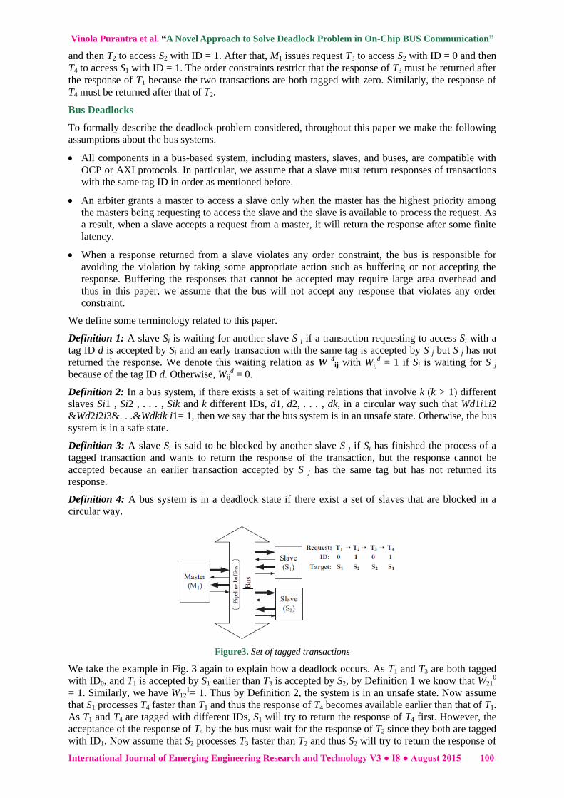
Vinola Purantra et al. “A Novel Approach to Solve Deadlock Problem in On-Chip BUS Communication”
International Journal of Emerging Engineering Research and Technology V3 ● I8 ● August 2015 100
and then T2 to access S2 with ID = 1. After that, M1 issues request T3 to access S2 with ID = 0 and then
T4 to access S1 with ID = 1. The order constraints restrict that the response of T3 must be returned after
the response of T1 because the two transactions are both tagged with zero. Similarly, the response of
T4 must be returned after that of T2.
Bus Deadlocks
To formally describe the deadlock problem considered, throughout this paper we make the following
assumptions about the bus systems.
All components in a bus-based system, including masters, slaves, and buses, are compatible with
OCP or AXI protocols. In particular, we assume that a slave must return responses of transactions
with the same tag ID in order as mentioned before.
An arbiter grants a master to access a slave only when the master has the highest priority among
the masters being requesting to access the slave and the slave is available to process the request. As
a result, when a slave accepts a request from a master, it will return the response after some finite
latency.
When a response returned from a slave violates any order constraint, the bus is responsible for
avoiding the violation by taking some appropriate action such as buffering or not accepting the
response. Buffering the responses that cannot be accepted may require large area overhead and
thus in this paper, we assume that the bus will not accept any response that violates any order
constraint.
We define some terminology related to this paper.
Definition 1: A slave Si is waiting for another slave S j if a transaction requesting to access Si with a
tag ID d is accepted by Si and an early transaction with the same tag is accepted by S j but S j has not
returned the response. We denote this waiting relation as W dij with Wij
d = 1 if Si is waiting for S j
because of the tag ID d. Otherwise, Wijd = 0.
Definition 2: In a bus system, if there exists a set of waiting relations that involve k (k > 1) different
slaves Si1 , Si2 , . . . , Sik and k different IDs, d1, d2, . . . , dk, in a circular way such that Wd1i1i2
&Wd2i2i3&. . .&Wdkik i1= 1, then we say that the bus system is in an unsafe state. Otherwise, the bus
system is in a safe state.
Definition 3: A slave Si is said to be blocked by another slave S j if Si has finished the process of a
tagged transaction and wants to return the response of the transaction, but the response cannot be
accepted because an earlier transaction accepted by S j has the same tag but has not returned its
response.
Definition 4: A bus system is in a deadlock state if there exist a set of slaves that are blocked in a
circular way.
Figure3. Set of tagged transactions
We take the example in Fig. 3 again to explain how a deadlock occurs. As T1 and T3 are both tagged
with ID0, and T1 is accepted by S1 earlier than T3 is accepted by S2, by Definition 1 we know that W210
= 1. Similarly, we have W121= 1. Thus by Definition 2, the system is in an unsafe state. Now assume
that S1 processes T4 faster than T1 and thus the response of T4 becomes available earlier than that of T1.
As T1 and T4 are tagged with different IDs, S1 will try to return the response of T4 first. However, the
acceptance of the response of T4 by the bus must wait for the response of T2 since they both are tagged
with ID1. Now assume that S2 processes T3 faster than T2 and thus S2 will try to return the response of

Vinola Purantra et al. “A Novel Approach to Solve Deadlock Problem in On-Chip BUS Communication”
101 International Journal of Emerging Engineering Research and Technology V3 ● I8 ● August 2015
T3 first. As T1 is not returned, T3 cannot be accepted because they both are tagged with ID0. Therefore,
the return of T3 from S2 cannot be accepted by the bus and thus S2 will keep trying to return T3, which
will then block the return of T2. Thus by Definition 3, S2 is blocked by S1. Unless S2 is able to switch
the return orders of T3 and T2, which is in general not supported by an IP core, S2 will continue
waiting for the bus. Similarly, the response of T4 cannot be accepted by the bus, which will also block
the return of T1 and thus S1 is blocked by S2. Therefore, a bus deadlock occurs. The above analysis
indicates that if a bus system is in an unsafe state, then the system will sink into a deadlock if the
return orders of the slaves results in a circular block situation.
The bus deadlock problem can be solved clearly by requesting masters not to issue tagged transactions
that may result in an unsafe state, or by constraining each slave to return all its responses of
transactions in their acceptances by the slave. However, a bus deadlock generally involves a set of IP
cores, and solving the deadlock problem at individual IP cores may over-solve the problem and thus
decrease the performance. We mentioned that both OCP and AXI require each slave to return
responses of transactions with the same tag ID in order. However, they also allow slaves to return
responses of transactions with different IDs out of order. As tagged transactions aim to improve
communication efficiency, solving the bus deadlock problem at the communication systems, i.e., the
buses should be more appropriate and efficient. In this paper, we deal with the bus deadlock problem
inside the on-chip buses. This enables legacy IPs with no deadlock consideration to be reusable
without the risk of falling into a deadlock, and the effort of designing new IPs is not increased because
of the consideration of a bus deadlock.
Previous Work for Bus Deadlock
Similar to an OS, one approach to detect a bus deadlock is to set a timer that will expire some clock
cycles later after a bus transaction is expected to be completed. However, to prevent the timer from
expiring when there is no bus deadlock, the timer must be set to accommodate any possible latency of
transactions. This will result in a long latency between the occurrence and the detection of a bus
deadlock and thus the communication efficiency may be drastically affected. The method in [8]
embeds a bus tracer in buses to monitors bus transactions. If the tracer detects a condition indicating
some transaction is waiting or retrying, a counter with a predetermined number starts to count down.
When the counter is decreased to zero, it is regarded as a deadlock occurs. With this method, a bus
deadlock can be detected with few clock cycles. However, the predetermined number is difficult to
determine appropriately. If the number is too small, designers may encounter the problem of over
detection, whereas if it is too large, the latency between the occurrence and the detection of deadlocks
is still long. Also, for both a timer and a bus tracer, after detecting the deadlock, some complicated
mechanism is required to resume the bus system to the state before the deadlock, which may require
large hardware overhead.
In [9], three methods are implemented to deal with the bus deadlock problem, namely the single-slave
scheme, the unique ID scheme, and the hybrid scheme. The main idea of these methods is to stall
some tagged transactions that may violate the order constraints. The single slave scheme stalls a
tagged transaction targeting a slave if another slave is being accessed by an uncompleted tagged
transaction. The unique ID scheme stalls requests whose IDs are already assigned to some
uncompleted transactions. These two schemes, respectively, restrict that at any time, at most one slave
can be accessed by tagged transactions, and each ID can be used by at most one tagged transaction.
The hybrid scheme combines the two schemes by allowing any tagged transaction that satisfies either
the single slave or the unique ID constraint. Though the communication efficiency can be improved,
this scheme still over-stalls many tagged transactions that will not cause any bus deadlock. We will
analyze this problem by using the proposed graph model later and show that our proposed technique
can result in much better performance than these schemes.
ON-CHIP BUS DESIGN
This section describes the architecture of the on-chip bus used in this paper. We will describe how a
transaction is processed inside the bus. Compared to previous bus designs [10]–[15], we emphasize
the supporting of various advanced transaction types in OCP and AXI. As shown in Fig. 4, our bus
supports single, burst, pipelined (outstanding), and tagged transactions. We divide the components of
the bus system into three parts: 1) the components for each master interface; 2) the components for
each slave interface; and 3) the components in the center that will be shared by all masters and slaves.
Fig. 4 shows a bus system with one master and one slave. If l masters (m slaves) are to be employed, l
(m) copies of the components in the master (slave) interface should be employed, whereas only one

Vinola Purantra et al. “A Novel Approach to Solve Deadlock Problem in On-Chip BUS Communication”
International Journal of Emerging Engineering Research and Technology V3 ● I8 ● August 2015 102
copy of the components in the center is needed.
A tagged transaction starts with a master issuing a request with an ID to the bus. In the request phase,
if the Request Buffer in the bus is not full, the bus acknowledges the master and the request is stored
in the Request Buffer. The Decoder then decodes the transaction address of the request, and the
Arbiter arbitrates whether the request can be granted to access the target slave. If it can be granted, the
Arbiter forwards the request to the slave by controlling the corresponding multiplexors, and the index
of the target slave is recorded in one of the Recorders, in the way that the transactions with the same
tag are recorded in the same Recorder. The number of Recorders is equal to the number of IDs that
the corresponding master can assign. Also the size of each Recorder is equal to the pipeline depth
such that it is just enough to record all transactions that are not completed.
The Request Busy Checker checks whether the request is completed or not to assist the arbitration.
For a write request, the corresponding write data are stored in the Write Data Buffer, and the Tagged
Transaction Access Controller controls the multiplexors to decide from which master the write data
are to be provided. After the slave accepts the request, it acknowledges the bus, and the
acknowledgment is forwarded to the Request Buffer under the control of the Arbiter.
In the response phase, the slave responds the bus with the read data for a read transaction or the
completion status of the written data for a write transaction. If the responses can be accepted, they are
stored in the Read Data and Write Status Buffer, which then acknowledges the slave. The tagged
trans-action access controller controls the multiplexors to decide from which slave the response is
provided and from which read data and write status buffer the acknowledgment comes. Finally, the
response is sent to the master when the master is able to receive it.
In the bus model, the masters and slaves are connected by the bus in a crossbar manner and thus
parallel transactions can be executed as long as no contention occurs. When more than one request
from different masters to access the same slave arrives simultaneously, the arbiter will determine
whether the request with the highest priority can be granted or not. If it cannot be granted, the arbiter
will start a new arbitration with possibly some priority updating (such as round robin). If it can be
granted, the request will be forwarded to the corresponding slave. Once a request is granted, it can be
processed in parallel with other granted requests. As a result, high communication parallelism can be
achieved by this bus design.
Figure4. Bus architecture supporting tagged transactions
Figure5. Prime edge and nonprime edge in BSG indicating Si is waiting for Sj because of IDd.

Vinola Purantra et al. “A Novel Approach to Solve Deadlock Problem in On-Chip BUS Communication”
103 International Journal of Emerging Engineering Research and Technology V3 ● I8 ● August 2015
BUS STATUS GRAPH
We now describe the proposed BSG model. A BSG contains two types of vertices, namely slave
vertices and ID vertices, and two types of edges, namely prime edges and nonprime edges. Each
vertex in a BSG represents a slave or a tag ID. Consider an SOC system containing m slaves and
employing totally n tag IDs. Without loss of generality, we denote the set of slave vertices as S = {S1,
S2….. Sm } and the set of ID vertices as ID = {ID0, ID1. . . IDn−1}. The same ID values tagged by
different masters are regarded as different IDs in the ID vertex set. A BSG representing this system
will contain m + n vertices. To distinguish the slave and ID vertices, we use a circle and a square to
represent a slave vertex and an ID vertex in a BSG. We do not model the masters in the graph. Later,
the rationale for this will become clear.
Each edge in the graph represents a transaction request that is accepted by a slave but is not
completed. A prime edge is one from an ID vertex to a slave vertex and a nonprime edge is one from
a slave to an ID. As shown in Fig. 5. A prime edge from vertex IDd to vertex Sj indicates that the
transaction corresponding to the edge is requesting to access Sj and is the first accepted transaction
among all currently accepted but not completed transactions with the tag IDd . A nonprime edge from
vertex Si to vertex IDd indicates that the corresponding transaction is targeting Si but is not the first
accepted transaction among the accepted but not completed transactions tagged with IDd . These
definitions implies that at any time there can be at most one prime edge associated with an ID vertex,
and each transaction corresponding to a nonprime edge must wait for the completion of the
transaction corresponding to the prime edge with the same ID.
(a) (b) (c) (d)
Figure6. Example of BSG indicating system is in unsafe state.
(a) (b) (c) (d)
Figure7. Example of BSG indicating system is in safe state.
For a BSG, when a transaction with tag IDd is accepted by a slave Sj, a prime edge from vertex IDd to
vertex Sj appears if there is no uncompleted transaction with the same IDd in the bus system.
Otherwise, a nonprime edge from vertex Sj to IDd appears which implies that the transaction must
wait for some other transaction to complete. Using our waiting relation notation, in Fig. 5 we have the
waiting relation Wd ij = 1. When one transaction corresponding to a prime edge is completed, the
prime edge will disappear, and one of the nonprime edges (if any) will become a prime edge, i.e., the
edge corresponding to the transaction that is accepted earliest among all the transactions that are
waiting for the just completed transaction will become a prime one. Based on the definition of a BSG,
we can see that a cycle in a BSG implies that a set of waiting relations exist in a circular way, which
indicates that the bus system is in an unsafe state. Take the transactions in the bus system in Fig. 3
again as an example.
Figure8. A cycle composed of multiple edges does not imply that the bus system is in an unsafe state.
Vinola Purantra et al. “A Novel Approach to Solve Deadlock Problem in On-Chip BUS Communication”
International Journal of Emerging Engineering Research and Technology V3 ● I8 ● August 2015 104
The SOC system contains two slaves, so there are two vertices in the slave vertex set, namely S1 and
S2. The IDs can be zero or one, so there are also two vertices in the ID vertex set, namely ID0 and
ID1 (respectively, refers to ID value zero and one). When the master in Fig. 3 first requests T1, a
prime edge from ID0 to S1 appears in the BSG as shown in Fig. 6(a). The master then requests T2
which accesses S2 with ID1. A prime edge from ID1 to S2 will appear after T2 is accepted by S2 as
shown in Fig. 6(b). When the master requests T3 which accesses S2 with ID0, there is one
uncompleted transaction (T1) tagged with ID0. Thus Fig. 6(c) shows a nonprime edge from S2 to ID0
appears after T3 is accepted by S2. Similarly, Fig. 6(d) shows that a nonprime edge from S1 to ID1
will appear after T4 is accepted by S1. In Fig. 6(d), a cycle exists in the BSG, and the bus system is in
an unsafe state that may lead to a bus deadlock.
Now consider the case when the request orders of the transactions in Fig. 3 are T1 → T4 → T2 → T3.
As Fig. 7(a) and (b) shows, there are no uncompleted transactions tagged with ID0 or ID 1 when T1
and T4 are accepted. Hence, two prime edges associated with S1 appear. Assume that when T2 and T3
are accepted, T4 and T1 are not completed yet. Then two nonprime edges will appear as shown in Fig.
7(c) and (d). In this case, no cycle exists in the BSG. Thus no matter how the responses from S1 and S2
are returned, no deadlock can occur.
From the definition of vertices and edges of a BSG and the examples given above, it appears that a
bus system is in an unsafe state when a cycle appears in the BSG. However, we have to consider that
multiple edges may exist between a slave vertex and an ID vertex of a BSG, and thus a cycle
composed of multiple edges between two vertices as shown in Fig. 8 may exist. As multiple edges can
appear between a pair of slaves and an ID only if the transactions corresponding to these edges are
issued by the same master because of the fact that IDs assigned by different masters are regarded as
different, and slaves must return responses of the transactions with the same ID in order, there cannot
be any deadlock among the transactions corresponding to these multiple edges. Thus, deadlock can
occur only when a cycle involving at least two slaves and two IDs. In this paper, we shall call a cycle
as a nontrivial cycle if it is a simple cycle involving multiple slave vertices and multiple ID vertices,
where a simple cycle is a cycle in which no vertex or edge appears more than once.
BUS DEADLOCK SOLUTION
In this paper, we propose a technique to solve the bus deadlock problem based on BSG. Because no
deadlock occurs if a bus system is always in a safe state, the proposed technique avoids deadlocks by
stalling requests that will result in nontrivial cycles in the BSG. A similar request stalling concept to
avoid deadlocks is also adopted in [9]. The main difference between our technique and those in [9] is
that under the help of BSG we can stall much less requests but can still guarantee that no deadlock
will occur.
(a) (b)
Figure9. Legal requests under single slave scheme.
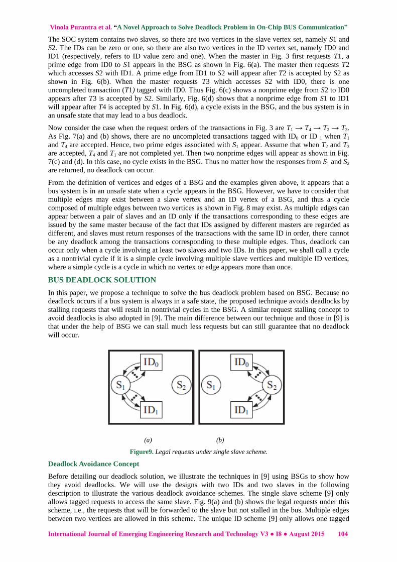
Deadlock Avoidance Concept
Before detailing our deadlock solution, we illustrate the techniques in [9] using BSGs to show how
they avoid deadlocks. We will use the designs with two IDs and two slaves in the following
description to illustrate the various deadlock avoidance schemes. The single slave scheme [9] only
allows tagged requests to access the same slave. Fig. 9(a) and (b) shows the legal requests under this
scheme, i.e., the requests that will be forwarded to the slave but not stalled in the bus. Multiple edges
between two vertices are allowed in this scheme. The unique ID scheme [9] only allows one tagged

Vinola Purantra et al. “A Novel Approach to Solve Deadlock Problem in On-Chip BUS Communication”
105 International Journal of Emerging Engineering Research and Technology V3 ● I8 ● August 2015
request for each ID. If there are k available IDs, at most k tagged requests can be accepted. Legal
requests under the unique ID scheme are shown in Fig. 10(a)–(d).
Figure10. Legal requests under unique ID scheme.
Figure11. Legal requests under hybrid scheme
The hybrid scheme [9] combines the above two schemes and allows multiple requests to the same
slave with the same ID in the unique ID basis, i.e., all requests tagged with the same ID must target
the same slave. Legal requests under the hybrid scheme are shown in Fig. 11(a)–(d). From these
graphs, we can see that many transactions that will not result in a deadlock cannot be forwarded to
slaves. For example, in Fig. 11(a), a request to access S2 with ID0 or ID1 can still be issued and
accepted by S2 without causing any deadlock. We next describe our deadlock solution. Our deadlock
avoidance approach, called the deadlock avoidance by least stalling (DALS), stalls a request only if
forwarding the request will form a nontrivial cycle in a BSG. Based on this idea, legal requests in a
design with two IDs and two slaves under our DALS are shown in Fig. 12, where we classify the
edges corresponding to requests targeting S1 and S2 with ID0 into edge sets A and B, respectively,
and classify those corresponding to requests targeting S2 and S1 with ID1 into edge sets C and D,
respectively. If any of the four request sets is empty, no nontrivial cycle exists in the BSG. Fig. 12(a)
and (b) shows the case of the edge set A being empty, where the first request tagged with ID1 targets
S2 in Fig. 12(a) and the first request tagged with ID1 targets S1 in Fig. 12(b). In both cases, the first
request tagged with ID0 target S2. These figures indicates that any new request belonging to sets B, C,
or D can be accepted with no risk of deadlock occurring. Fig. 12(c)–(h) shows the legal requests in the
cases that edge sets B, C, and D are empty, respectively.
In addition, in some cases the proposed DALS also forwards requests in the fourth edge set. Consider
Fig. 12(a) again. If a new request accessing S1 and tagged with ID0 is accepted by S1, an edge in edge
set A appears. This edge must be a nonprime edge from S1 to ID0 because a prime edge associated
with ID0 already exists. Thus no counter-clockwise nontrivial cycle can occur in Fig. 12(a). Now if all
the requests in C are accepted by S2 earlier than all the requests in D are accepted by S1, the edges in
D must be nonprime edges before all requests in C are completed. Therefore, no clockwise nontrivial
cycle can occur in Fig. 12(a) either. As a result, no deadlock can occur even if a new request in A is
accepted. We show the results of this analysis in Fig. 12(i) where all requests in C are marked in red
and all requests in D are marked in green with the order that all red edges are requested and accepted
before all green edges. The dashed edges in A indicate the new requests that can be issued in this case.
Similarly, as shown in Fig. 12(j)–(l), dashed requests in request sets B, C, and D can be, respectively,
issued and accepted by slaves if the requests marked with red are accepted earlier than those marked
with green. In our proposed DALS, we do not stall any dashed request in Fig. 12(i)–(l).

Vinola Purantra et al. “A Novel Approach to Solve Deadlock Problem in On-Chip BUS Communication”
International Journal of Emerging Engineering Research and Technology V3 ● I8 ● August 2015 106
Figure12. Legal requests under our DALS.
It can be verified that in Fig. 3, our DALS does not stall any request until the fourth transaction is
requested, whereas the single slave scheme will stall the second and both the unique ID and the hybrid
schemes will stall the third transactions. If the request T3 are accepted before T1 [in Fig. 12(l)], the
fourth request T4 could also be accepted by DALS.
Hardware Implementation
The hardware design of our DALS attempts to stall the least number of transactions. In addition, we
also target to complete the decision of whether to stall a transaction in one clock cycle. We propose a
hardware implementation that contains a number of waiting relation detectors and a number of unsafe
state predictors which altogether requires only one clock cycle for the stall decision. Each waiting
relation detector determines whether a pair of slaves has a waiting relation between them. According
to the results of these detectors, the unsafe state predictors predict whether forwarding a request will
result in an unsafe state. These designs are detailed next.
Waiting Relation Detectors
As mentioned in Section 3, we allocate a recorder for each ID in the bus system, and the index of a
target slave of a tagged transaction is recorded in a corresponding recorder when the transaction is
accepted by the slave. Responses from different slaves with the same ID must be returned in the order
that they are recorded in the recorder. The hardware implementation of the waiting relation detector
detecting Wd ij is shown in Fig. 13. The left side shows a recorder to record the transactions with tag
IDd . The recorder is implemented using a shift queue with the following features.
1. The indices of the slaves accepted are put in the recorder in a first-in-first-out manner.
2. The first entry (P0) always contains the index of the slave that accepts the earliest transaction
among all the accepted but not completed transactions with tag IDd , which is corresponding to the
prime edge associated with IDd in the corresponding BSG.
3. When the response from the slave recorded in P0 is returned, a shift operation is performed to
remove the index of the slave from the recorder and all the indices of the slaves in the remaining
entries of the buffer are shifted toward P0 by one position.

Vinola Purantra et al. “A Novel Approach to Solve Deadlock Problem in On-Chip BUS Communication”
107 International Journal of Emerging Engineering Research and Technology V3 ● I8 ● August 2015
Figure13. Recorder and waiting relation detector.
The P0 and P1 entries of the IDd recorder in Fig. 13 shows that a request to Sj with IDd is first
accepted by Sj and then a request to Si with IDd is accepted by Si. Now a new transaction also tagged
with IDd is requested. The proposed waiting relation detector will detect the waiting relations of
already accepted requests as well as the waiting relations if the new request is accepted as described
below. As shown in Fig. 13, the waiting relation detector for Wdij contains: 1) l-1 blocks of circuits,
where l is the size of the recorder; 2) a comparator feeding the l-1 blocks; and 3) an OR gate taking
the OR operation of the outputs of the l-1 blocks. The comparator outside the blocks determines
whether the new request is targeting Si or not. The first comparator in block 1 determines whether the
slave ID recorded in P0 is Sj or not, the remaining l-1 comparators determine whether Si is stored in
any location other than P0. This block determines whether Si is waiting or will wait for Sj in P0 if the
new request is accepted. Similarly, the circuits in block 2 detect whether Si is waiting or will wait for
Sj in P1 and so on. Thus all blocks together can detect whether the relation Wd ij already exists or will
exist if the new request is accepted.
Unsafe State Predictors
In a system containing m slaves and n IDs, a nontrivial circular waiting cycle may occur among
any k [2≤ k ≤ min (m, n)] slaves. We define a cycle group as a set of nontrivial circular waiting cycles
that occur among the same slaves with the same waiting order, regardless of which IDs they are
tagged. For, example both the waiting cycles W121& W23
2 & W313= 1 and W12
2& W233& W31
4= 1 occur
amongS1, S2, and S3 with the waiting orders of S1 waiting for S2, S2 waiting for S3, and S3 waiting
for S1, so they are in the same cycle group. In contrast, the waiting cycles W121& W23
2& W313= 1 and
W131& W32
1& W211= 1 are indifferent groups. In our DALS implementation, we allocate an unsafe
state predictor for each cycle group to predict whether any nontrivial circular waiting cycle in the
cycle group exists. We thus can predict the occurrence of any nontrivial circular waiting cycle in a
system using all unsafe state predictors together. The implementation of the unsafe state predictors is
based on monitoring the waiting relations from the waiting relation detectors. We take the unsafe state
predictor for the cycle group W12d1& W23
d2&. . .& Wkldk= 1 as an example for illustration, where d1,
d2, . . . , and dk are k different IDs. The occurrence of all nontrivial circular waiting cycles in other
cycle groups can be predicted with the similar concept.

Vinola Purantra et al. “A Novel Approach to Solve Deadlock Problem in On-Chip BUS Communication”
International Journal of Emerging Engineering Research and Technology V3 ● I8 ● August 2015 108
Simulation Results
CONCLUSION
Advanced communication protocols such as AXI and OCP can greatly improve the overall
performance of a large VLSI system. However, the whole system may sink into a deadlock if
designers do not carefully handle the advanced transactions. In this paper, we proposed a new graph
model called the BSG to model the behavior of a bus system that can describe the necessary and
sufficient condition for an unsafe state to occur. We then proposed a technique to solve the deadlock
problem.
REFERENCES
[1] Advanced Microcontroller Bus Architecture Specification.(1997) [Online]. Available:
http://www.arm.com
[2] Open Core Protocol Specification.(2006) [Online]. Available: http:// www.ocpip.org/ home
[3] A. T. Tran and B. M. Bass, “RoShaQ: High-performance on-chip router with shared queues,” in
Proc. IEEE 29th Int. Conf. Comput. Design, Oct. 2011, pp. 232–238.
[4] J. Shao and B. T. Davis, “A burst scheduling access reordering mechanism,” in Proc. IEEE 13th
Int. Symp. High Perform. Comput. Archit., Feb. 2007, pp. 285–294.
[5] J. Pang, L. Yang, L. Shi, T. Zhang, D. Wang, and C. Hou, “A priority- expression-based burst
scheduling of memory reordering access,” in Proc. Int. Conf. Embedded Comput. Syst.,
Archit., Model. Simul., Jul. 2008, pp. 203–209.
[6] X. Xiao and J. J. Lee, “A true O(1) parallel deadlock detection algorithm for single-unit resource
systems and its hardware implementation,” IEEE Trans. Parallel Distrib. Syst., vol. 21, no. 1, pp.
4–19, Jan. 2010.
[7] A. Silberschatz, P. B. Galvin, and G. Gagen, Operating System Concepts,7th ed. New York,
USA: Wiley, 1993.
[8] T. S. Cummins, “Method and apparatus for detecting a bus deadlock in an electronic system,”
U.S. Patent 6 292 910, Sep. 18, 2001.
[9] Technical Reference Manual of PrimeCell AXI Configurable Intercon- nect (PL300), ARM,
Cambridge, U.K., 2010.
[10] K. Lahiri, A. Raghunathan, and G. Lakshminarayana, “The LOTTERY- BUS on-chip
communication architecture,” IEEE Trans. Very Large Scale Integr. (VLSI) Syst., vol. 14, no.
6, pp. 596–608, Jun. 2006.
[11] K. Sekar, K. Lahiri, A. Raghunathan, and S. Dey, “Dynamically config- urable bus topologies
for high-performance on-chip communication,” IEEE Trans. Very Large Scale Integr. (VLSI)
Syst., vol. 16, no. 10, pp. 1413–1426, Oct. 2008.
[12] F.-M. Xiao, D.-S. Li. G.-M. Du, Y.-K. Song, D.-L. Zhang, and M.-L. Gao, “Design of
AXI bus based MPSoC on FPGA,” in Proc. 3rd Int. Conf. Anti-Counterfeit., Security,
Identificat. Commun., Aug. 2009, pp. 560–564.
[13] H.-W. Wang, C.-S. Lai, C.-F. Wu, S.-A. Hwang, and Y.-H. Lin, “On- chip Interconnection
Design and SoC Integration with OCP,” in Proc. IEEE Int. Symp. VLSI Design, Autom., Test,
Apr. 2008, pp. 25–28.
[14] N. Y.-C. Chang, Y.-Z. Liao, and T.-S. Chang, “Analysis of shared-link

Vinola Purantra et al. “A Novel Approach to Solve Deadlock Problem in On-Chip BUS Communication”
109 International Journal of Emerging Engineering Research and Technology V3 ● I8 ● August 2015
[15] AXI,” IET Comput. Digit. Tech., vol. 3, no. 4, pp. 373–383, Jul. 2009.
[16] O. Ogawa, S. Bayon de Noyer, P. Chauvet, K. Shinohara, Y. Watanabe, H. Niizuma, T. Sasaki,
and Y. Takai, “A practical approach for bus architecture optimization at transaction level,” in
Proc. Design, Autom., Test Europe Conf. Exhibit., 2003, pp. 176–181.
[17] Synopsys Design Compiler. (2010) [Online] Available: http:// www.synopsys.com/ Tools/
Implementation/RTLSynthesis/Pages/ default.aspx
AUTHORS’ BIOGRAPHY
Ms. VINOLA PURANTRA has completed her B.TECH. in Electronics &
Communication Engineering, from Siddhartha Institute of Engineering and
Technology, JNTU , Hyderabad. Presently she is pursuing her Masters in VLSI
DESIGN SYSTEM, from Siddhartha Institute of Engineering and Technology,
Hyderabad, TS, India. Her areas of interest are VLSI system design and digital design.
Email: [email protected]
Mr. D. SUBBA RAO has completed M.Tech (Embedded) from SRM University,
Chennai. Phd (Embedded) from VBS Purvanchal University, Jaunpur, UP. He is
having 13 years of experience in Academic, Currently working as Associate Professor
in Dept. of E.C.E and is being chaired as head of the department for E.C.E discipline
at Siddhartha Institute of Engineering and Technology, Hyderabad, TS, India. Email:
Mr. S.SUBBANNA has completed B.Tech (ECE) from VITS Institute of Technology
and science, J.N.T.U, Nellore. M.Tech (DECS) from Sri Indu Institute of Technology,
J.N.T.U, Hyderabad. He is having 7 years of experience in Academic, Currently
working as Associate Professor in Dept of E.C.E, at Siddhartha Institute of
Engineering and Technology, Hyderabad, TS, India.his areas of interest in
communication system. Email: [email protected]