Embed Size (px)
Citation preview
A Novel Approach to Reduce Delay and Power inVLSI Interconnects
Submitted in partial fulfillment of
the requirements for the degree of
Master of Science (by Research)in
Electronics and Communication Engineering
by
Sandeep Saini<saini [email protected]>
http://web.iiit.ac.in/∼saini sandeep
Under Guidance of
Dr M. B. Srinivas
Centre for VLSI and Embedded System Technologies
International Institute of Information Technology
Hyderabad, INDIA
May, 2010

© Copyright by Sandeep Saini, 2009

INTERNATIONAL INSTITUTE OF INFORMATION TECHNOLOGYHyderabad, India
CERTIFICATE
It is certified that the work contained in this thesis, titled “A Novel Approach to Reduce Delay andPower in VLSI Interconnects” by Sandeep Saini, has been carried out under my supervision and is notsubmitted elsewhere for a degree.
Date Advisor: M B Srinivas

To my Parents

Acknowledgement
I am greatly indebted to my advisor, Dr. M. B. Srinivas. Sir, I could not have realized mypotential without your invaluable guidance, consistent encouragement and emphasis on quality of theresearch contribution.Professor Srinivas is a wonderful teacher and person to work with. ProfessorSrinivas has shared his profound knowledge and professional manner of conducting research. I am verythankful to him for all the time he devoted to scientific discussions with me, as well as for his constantencouragement.
Special thanks to J.V.R.Ravindra and Srihari for the brain-storming sessions we had, and forguiding me in right direction right from the beginning of my research work.I appreciate very much theirinvaluable assistance.
To my lab mates through Bachelors and Masters, I owe big thanks for the fun-centered atmo-sphere in CVEST and OBH. I have been fortunate enough to meet Gaurav, Maneesh, Khosla, Bajaj,Rishi, Manan, Handa, Ramavtar, Sumit, Bhatt, Anshul, Bharat, Avinash, Kashi, Mohit, Abheet, Gopal.All CVEST lab mates were equally supportive.
Finally, and most importantly, this thesis is dedicated to my parents, whose unconditional loveand support I have enjoyed throughout my life.
v
Abstract
Interconnects play a major role in deep submicron (DSM) technologies such as 90nm and
below. While gate delay dominated interconnect delay in earlier technologies, it is no longer the case
and delays associated with interconnects are becoming increasingly important. This is because in DSM
technologies, interconnect can no longer be seen as a simple resistor but the associated parasitics such
as capacitance and inductance also need to be considered. Thus any signal propagating through such an
interconnect can be expected to be delayed.
Buffer insertion is one popular technique to reduce (eliminate) the delay. In this technique,
buffers are placed at regular intervals along an interconnect that seeks to restore the signal each time it
is affected by the parasitics. However, buffers themselves have certain switching time that contributes to
delay. A large number of such buffers along an interconnect can thus contribute to overall delay to signal
propagation. Also buffer switching contributes to power dissipation. Further in DSM technologies,
leakage power is a major problem and buffers may consume power even when they are not switching.
Thus there is an urgent need to evolve techniques that while reducing the overall delay, also consume
lesser power, dynamic as well as static.
In this thesis, Schmitt trigger as an alternate to buffer to reduce delay and power in intercon-
nects is examined. The most favorable feature of Schmitt trigger is it’s adjustable threshold voltage, and
since it can be controlled, the threshold voltage can be chosen to be above or below Vdd/2 a voltage at
which buffer normally operate. Thus a Schmitt trigger can be designed to switch faster than a buffer
leading to a reduction in delay. Further, the adjustable low-voltage threshold of the schmitt trigger han-
dles more noise and voltage glitches as compared to buffer. Proposed approach is first implemented for
linear interconnects of various lengths and then on buses which are groups of interconnects. It is shown
that the proposed approach is better in terms of delay, power and crosstalk noise reduction compared to
that of buffers.
vi

List of Publications
1 Sandeep Saini, A. Mahesh Kumar, Sreehari Veeramachaneni, M.B.Srinivas, ”Alternative ap-proach to Buffer Insertion for Delay and Power Reduction in VLSI Interconnects”, accepted in,Journal of Low Power Electronics, to be published by American Scientific Publishers.
2 Sandeep Saini, A. Mahesh Kumar, Sreehari Veeramachaneni, M.B.Srinivas, ”Schmitt trigger asan alternate to buffer for delay reduction in on chip buses”, Tencon 2009. 23rd to 26th Nov 2009,Singapore, pages 1-5.
3 Sandeep Saini, A. Mahesh Kumar, Sreehari Veeramachaneni, M.B.Srinivas, ”Alternative ap-proach to Buffer Insertion for Delay and Power Reduction in VLSI Interconnects”, VLSI design2010, 3rd to 7th January 2010, Banglore, pages 411-416.
vii

Contents
Chapter Page
1 Introduction . . . . . . . . . . . . . . . . . . . . . . . . . . . . . . . . . . . . . . . . . . 11.1 Objective . . . . . . . . . . . . . . . . . . . . . . . . . . . . . . . . . . . . . . . . . 11.2 Motivation . . . . . . . . . . . . . . . . . . . . . . . . . . . . . . . . . . . . . . . . . 11.3 Literature Survey . . . . . . . . . . . . . . . . . . . . . . . . . . . . . . . . . . . . . 3
1.3.1 Need for a better approach . . . . . . . . . . . . . . . . . . . . . . . . . . . . 51.4 Contribution of the Thesis . . . . . . . . . . . . . . . . . . . . . . . . . . . . . . . . 61.5 Organization of the Thesis . . . . . . . . . . . . . . . . . . . . . . . . . . . . . . . . 6
2 Introduction to Interconnects . . . . . . . . . . . . . . . . . . . . . . . . . . . . . . . . . . 82.1 Design Flows for DSM ASICs . . . . . . . . . . . . . . . . . . . . . . . . . . . . . . 82.2 Interconnect Design Criteria . . . . . . . . . . . . . . . . . . . . . . . . . . . . . . . 10
2.2.1 Delay . . . . . . . . . . . . . . . . . . . . . . . . . . . . . . . . . . . . . . . 102.2.2 Power Dissipation . . . . . . . . . . . . . . . . . . . . . . . . . . . . . . . . 112.2.3 Noise . . . . . . . . . . . . . . . . . . . . . . . . . . . . . . . . . . . . . . . 112.2.4 Physical Area . . . . . . . . . . . . . . . . . . . . . . . . . . . . . . . . . . 12
2.3 Interconnect Characteristics . . . . . . . . . . . . . . . . . . . . . . . . . . . . . . . . 122.3.1 Resistance . . . . . . . . . . . . . . . . . . . . . . . . . . . . . . . . . . . . 13
2.3.1.1 Diffusion barrier . . . . . . . . . . . . . . . . . . . . . . . . . . . . 132.3.1.2 Surface and grain boundary scattering . . . . . . . . . . . . . . . . 142.3.1.3 Temperature effect . . . . . . . . . . . . . . . . . . . . . . . . . . . 142.3.1.4 High frequency effects . . . . . . . . . . . . . . . . . . . . . . . . . 14
2.3.2 Capacitance . . . . . . . . . . . . . . . . . . . . . . . . . . . . . . . . . . . . 162.3.3 Inductance . . . . . . . . . . . . . . . . . . . . . . . . . . . . . . . . . . . . 16
2.3.3.1 Partial inductance . . . . . . . . . . . . . . . . . . . . . . . . . . . 172.3.3.2 Loop-based inductance . . . . . . . . . . . . . . . . . . . . . . . . 172.3.3.3 High frequency effects . . . . . . . . . . . . . . . . . . . . . . . . 17
2.4 Interconnect Models . . . . . . . . . . . . . . . . . . . . . . . . . . . . . . . . . . . 182.4.1 Single Interconnect . . . . . . . . . . . . . . . . . . . . . . . . . . . . . . . . 18
2.4.1.1 Lumped models . . . . . . . . . . . . . . . . . . . . . . . . . . . . 182.4.1.2 Distributed models . . . . . . . . . . . . . . . . . . . . . . . . . . 192.4.1.3 Lumped representation of distributed interconnects . . . . . . . . . 202.4.1.4 Modeling frequency dependent effects . . . . . . . . . . . . . . . . 21
2.4.2 Parallel Coupled Interconnects . . . . . . . . . . . . . . . . . . . . . . . . . 212.5 Design Methodologies for Interconnect . . . . . . . . . . . . . . . . . . . . . . . . . 23
2.5.1 Constructing an Interconnect Tree . . . . . . . . . . . . . . . . . . . . . . . . 23
viii

CONTENTS ix
2.5.2 Wire Sizing, Shaping, and Spacing . . . . . . . . . . . . . . . . . . . . . . . 242.5.3 Repeater Insertion . . . . . . . . . . . . . . . . . . . . . . . . . . . . . . . . 252.5.4 Shielding Techniques . . . . . . . . . . . . . . . . . . . . . . . . . . . . . . . 262.5.5 Net-Ordering and Wire Swizzling . . . . . . . . . . . . . . . . . . . . . . . . 27
3 Buffer Insertion . . . . . . . . . . . . . . . . . . . . . . . . . . . . . . . . . . . . . . . . 283.1 Background . . . . . . . . . . . . . . . . . . . . . . . . . . . . . . . . . . . . . . . . 293.2 Repeater / buffer insertion process: An overview . . . . . . . . . . . . . . . . . . . . 303.3 Propagation delay . . . . . . . . . . . . . . . . . . . . . . . . . . . . . . . . . . . . . 313.4 Power dissipation . . . . . . . . . . . . . . . . . . . . . . . . . . . . . . . . . . . . . 34
3.4.1 Short-circuit power dissipation . . . . . . . . . . . . . . . . . . . . . . . . . 353.4.2 Dynamic power dissipation . . . . . . . . . . . . . . . . . . . . . . . . . . . 363.4.3 Total power dissipation . . . . . . . . . . . . . . . . . . . . . . . . . . . . . . 37
3.5 Area of the repeater system . . . . . . . . . . . . . . . . . . . . . . . . . . . . . . . 383.6 Design criteria for interconnect within a repeater system . . . . . . . . . . . . . . . . 41
3.6.1 Constrained systems . . . . . . . . . . . . . . . . . . . . . . . . . . . . . . . 413.6.2 Unconstrained systems . . . . . . . . . . . . . . . . . . . . . . . . . . . . . . 41
3.6.2.1 Power-delay-product design criterion . . . . . . . . . . . . . . . . . 413.6.2.2 Power-delay-area-product design criterion . . . . . . . . . . . . . . 42
3.7 Application of interconnect design methodology . . . . . . . . . . . . . . . . . . . . . 423.8 Need for a better approach . . . . . . . . . . . . . . . . . . . . . . . . . . . . . . . . 44
4 Schmitt Trigger as an alternate to Buffer . . . . . . . . . . . . . . . . . . . . . . . . . . . . 454.1 Classical Schmitt Trigger . . . . . . . . . . . . . . . . . . . . . . . . . . . . . . . . . 454.2 Hysteresis in Schmitt Trigger . . . . . . . . . . . . . . . . . . . . . . . . . . . . . . . 464.3 CMOS Schmitt Trigger . . . . . . . . . . . . . . . . . . . . . . . . . . . . . . . . . . 464.4 Low Voltage Schmitt Trigger . . . . . . . . . . . . . . . . . . . . . . . . . . . . . . . 504.5 CMOS buffer . . . . . . . . . . . . . . . . . . . . . . . . . . . . . . . . . . . . . . . 504.6 Schmitt trigger as an alternate to buffer Insertion . . . . . . . . . . . . . . . . . . . . 534.7 Conclusions . . . . . . . . . . . . . . . . . . . . . . . . . . . . . . . . . . . . . . . . 54
5 Results and Discussion . . . . . . . . . . . . . . . . . . . . . . . . . . . . . . . . . . . . . 555.1 NTRS 1997 predictions. . . . . . . . . . . . . . . . . . . . . . . . . . . . . . . . . . 555.2 Signal Propagation on a Linear Interconnect . . . . . . . . . . . . . . . . . . . . . . . 56
5.2.1 Types of interconnects . . . . . . . . . . . . . . . . . . . . . . . . . . . . . . 565.3 Effect of Buffer Insertion on Delay, Noise and Power Reduction . . . . . . . . . . . . 60
5.3.1 Delay Reduction using Buffer Insertion . . . . . . . . . . . . . . . . . . . . . 625.3.2 Noise and Power reduction using Buffer Insertion . . . . . . . . . . . . . . . . 64
5.4 Effect of Schmitt trigger on delay, noise and power reduction in Linear Interconnects . 685.4.1 Delay reductions with Schmitt trigger . . . . . . . . . . . . . . . . . . . . . . 695.4.2 Noise and power reduction with Schmitt trigger approach . . . . . . . . . . . . 71
5.5 Replacement of Buffers in Buses . . . . . . . . . . . . . . . . . . . . . . . . . . . . . 745.5.1 Signal Propagation in Buses . . . . . . . . . . . . . . . . . . . . . . . . . . . 745.5.2 Definitions and Related Work . . . . . . . . . . . . . . . . . . . . . . . . . . 77
5.5.2.1 Low Power Coding . . . . . . . . . . . . . . . . . . . . . . . . . . 775.5.2.2 Crosstalk Avoidance Coding . . . . . . . . . . . . . . . . . . . . . 775.5.2.3 Error Control Coding . . . . . . . . . . . . . . . . . . . . . . . . . 78

x CONTENTS
5.5.2.4 CAC coding Schemes . . . . . . . . . . . . . . . . . . . . . . . . . 785.5.2.5 Relationship between delay and crosstalk . . . . . . . . . . . . . . . 785.5.2.6 Interconnect Power Model . . . . . . . . . . . . . . . . . . . . . . 80
5.5.3 Comparison with existing bus coding technique . . . . . . . . . . . . . . . . . 815.6 Conclusion . . . . . . . . . . . . . . . . . . . . . . . . . . . . . . . . . . . . . . . . 82
6 Conclusions and Future Work . . . . . . . . . . . . . . . . . . . . . . . . . . . . . . . . . 856.1 Scope of further work . . . . . . . . . . . . . . . . . . . . . . . . . . . . . . . . . . . 85
Bibliography . . . . . . . . . . . . . . . . . . . . . . . . . . . . . . . . . . . . . . . . . . . . 86

List of Figures
Figure Page
1.1 The waveform for an 8 bit wide 1 mm long bus at 65nm technology . . . . . . . . . . 21.2 Percentage of nets requiring buffers. M3 and M6 represent nets on third and sixth metal
layer in a six metal layer technology. . . . . . . . . . . . . . . . . . . . . . . . . . . . 41.3 Buffers as a percentage of the total cell count for the chip. . . . . . . . . . . . . . . . . 51.4 Hysteresis in Schmitt trigger. . . . . . . . . . . . . . . . . . . . . . . . . . . . . . . . 6
2.1 A conventional ASIC design flow. . . . . . . . . . . . . . . . . . . . . . . . . . . . . 92.2 A data path in a synchronous digital system . . . . . . . . . . . . . . . . . . . . . . . 102.3 Components of dynamic power dissipation due to different capacitance sources: gate
capacitance, diffusion capacitance, and interconnect capacitance. . . . . . . . . . . . . 112.4 Interconnect coupling noise. . . . . . . . . . . . . . . . . . . . . . . . . . . . . . . . 122.5 Cross section of an on-chip copper interconnect. . . . . . . . . . . . . . . . . . . . . . 132.6 Current distribution in the cross section of an interconnect at high frequencies. Darker
color indicates higher current density. . . . . . . . . . . . . . . . . . . . . . . . . . . 152.7 Skin depth of Cu as a function of frequency. . . . . . . . . . . . . . . . . . . . . . . . 152.8 Current distributions in the cross section of two parallel wires at high frequencies due
to the proximity effect. . . . . . . . . . . . . . . . . . . . . . . . . . . . . . . . . . . 182.9 Lumped interconnect models. . . . . . . . . . . . . . . . . . . . . . . . . . . . . . . . 192.10 Circuit models of transmission lines. . . . . . . . . . . . . . . . . . . . . . . . . . . . 202.11 Modeling frequency dependent impedance with lumped elements. . . . . . . . . . . . 212.12 Decoupling multiple parallel coupled interconnects. . . . . . . . . . . . . . . . . . . . 222.13 An example of an A-tree. . . . . . . . . . . . . . . . . . . . . . . . . . . . . . . . . . 242.14 Shaping interconnect to minimize delay. . . . . . . . . . . . . . . . . . . . . . . . . . 242.15 Staggering repeaters to reduce the worst case delay and crosstalk noise. . . . . . . . . 252.16 Buffered interconnect tree. . . . . . . . . . . . . . . . . . . . . . . . . . . . . . . . . 262.17 Examples of net-ordering and wire swizzling. . . . . . . . . . . . . . . . . . . . . . . 27
3.1 Comparisions of Interconnect delay to gate delay . . . . . . . . . . . . . . . . . . . . 283.2 Minimum signal propagation delay and transient power dissipation as a function of line
width for a repeater system. . . . . . . . . . . . . . . . . . . . . . . . . . . . . . . . . 303.3 Uniform repeater system driving a distributed RC interconnect. . . . . . . . . . . . . . 313.4 Wire sizing in a repeater insertion system . . . . . . . . . . . . . . . . . . . . . . . . 313.5 Optimum numbers of repeaters for minimum propagation delay for different line widths. 333.6 Optimum repeater size for minimum propagation delay for different line widths. . . . . 343.7 Minimum signal propagation delay as a function of interconnect width (l=5mm). . . . 35
xi

xii LIST OF FIGURES
3.8 Minimum signal delay as a function of interconnects width for different line lengths. . 363.9 Dynamic power dissipation as a function of interconnect width for l=20 mm. . . . . . 373.10 Total transient power dissipation as a function of interconnects width. . . . . . . . . . 383.11 Interconnect area as a function of interconnects width for different line lengths. . . . . 393.12 Total area of the repeaters as a function of the interconnect width for different line lengths. 403.13 Product of interconnect and transistor area as a function of the interconnect width for
different line lengths. . . . . . . . . . . . . . . . . . . . . . . . . . . . . . . . . . . . 40
4.1 Schmitt trigger implementation with comparator . . . . . . . . . . . . . . . . . . . . . 454.2 Hysteresis in conventional Schmitt trigger. . . . . . . . . . . . . . . . . . . . . . . . . 474.3 . . . . . . . . . . . . . . . . . . . . . . . . . . . . . . . . . . . . . . . . . . . . . . 474.4 N-subcircuit driven by a voltage source: (a) circuit; (b) current-voltage characteristic;
(c) superposition of N- and P-subcircuit characteristics. . . . . . . . . . . . . . . . . . 484.5 1 V CMOS Schmitt trigger circuit . . . . . . . . . . . . . . . . . . . . . . . . . . . . 514.6 0.4 V CMOS Schmitt trigger circuit derived from 1 V Schmitt trigger . . . . . . . . . 514.7 Measured hysterisis characteristics of 0.4 V CMOS Schmitt trigger circuit, and mea-
sured input-output waveform characteristics a Measured hysterisis characteristic of 0.4V CMOS Schmitt trigger circuit b Measured input-output (Vin-Vout2) waveform char-acteristics . . . . . . . . . . . . . . . . . . . . . . . . . . . . . . . . . . . . . . . . . 52
4.8 CMOS buffer. . . . . . . . . . . . . . . . . . . . . . . . . . . . . . . . . . . . . . . . 524.9 4 bit bus with buffers to restore signals. . . . . . . . . . . . . . . . . . . . . . . . . . 53
5.1 An RC interconnect . . . . . . . . . . . . . . . . . . . . . . . . . . . . . . . . . . . . 575.2 Interconnect structure used for simulations . . . . . . . . . . . . . . . . . . . . . . . . 575.3 Output end signals on a 2mm, 5mm and 10mm RC interconnect at 180nm technology. 605.4 Output end signals on a 2mm, 5mm and 10mm RLC interconnect at 180nm technology. 615.5 Output end signals on a 2mm, 5mm and 10mm RLC interconnect at 90nm technology. 615.6 Output end signals on a 2mm, 5mm and 10mm RLC interconnect at 65nm technology. 625.7 Buffers inserted in an RLC interconnect. . . . . . . . . . . . . . . . . . . . . . . . . . 635.8 Delay reduction in 2mm interconnect with triangular input. . . . . . . . . . . . . . . . 635.9 Delay reduction in 2mm interconnect with square wave input. . . . . . . . . . . . . . 645.10 Delay reduction in 5mm interconnect with square wave input. . . . . . . . . . . . . . 655.11 Delay reduction in 10mm interconnect with square wave input. . . . . . . . . . . . . . 655.12 . . . . . . . . . . . . . . . . . . . . . . . . . . . . . . . . . . . . . . . . . . . . . . 675.13 . . . . . . . . . . . . . . . . . . . . . . . . . . . . . . . . . . . . . . . . . . . . . . 675.14 Delay reduction using Schmitt trigger approach in 2mm interconnect with square wave
input. . . . . . . . . . . . . . . . . . . . . . . . . . . . . . . . . . . . . . . . . . . . 695.15 Delay reduction using Schmitt trigger approach in 5mm interconnect with square wave
input. . . . . . . . . . . . . . . . . . . . . . . . . . . . . . . . . . . . . . . . . . . . 705.16 Delay reduction using Schmitt trigger approach in 10mm interconnect with square wave
input. . . . . . . . . . . . . . . . . . . . . . . . . . . . . . . . . . . . . . . . . . . . 705.17 Noise reduction using schmitt trigger . . . . . . . . . . . . . . . . . . . . . . . . . . . 725.18 Behavior of buffer and Schmitt trigger towards a noisy signal. . . . . . . . . . . . . . 735.19 Data transfer on an 8 bit data bus. . . . . . . . . . . . . . . . . . . . . . . . . . . . . 755.20 Data transfer on an 8 bit data bus in 65nm technology. . . . . . . . . . . . . . . . . . . 765.21 A 3 Bit to 4 wire coder . . . . . . . . . . . . . . . . . . . . . . . . . . . . . . . . . . 79

LIST OF FIGURES xiii
5.22 Transition Probability Graph . . . . . . . . . . . . . . . . . . . . . . . . . . . . . . . 815.23 Example of Transition Probability Graph . . . . . . . . . . . . . . . . . . . . . . . . . 825.24 Data signals rectified using Schmitt trigger approach in an 8 bit data bus. . . . . . . . . 83

List of Tables
Table Page
3.1 Uniform repeater system for different optimization criteria . . . . . . . . . . . . . . . 43
5.1 Projected advances in CMOS chip performance . . . . . . . . . . . . . . . . . . . . . 565.2 Interconnect dimensions . . . . . . . . . . . . . . . . . . . . . . . . . . . . . . . . . 585.3 Interconnect Resistance, Inductance and Capacitance values . . . . . . . . . . . . . . 595.4 Propagation delay values for an interconnect of different length with and without buffer
insertion . . . . . . . . . . . . . . . . . . . . . . . . . . . . . . . . . . . . . . . . . . 665.5 Power consumption values for an interconnect of different length with and without
buffer insertion approach. . . . . . . . . . . . . . . . . . . . . . . . . . . . . . . . . . 685.6 Propagation delay values for an interconnect of different length with buffer insertion
and delay reduction using Schmitt trigger approach . . . . . . . . . . . . . . . . . . . 715.7 Power consumption values for an interconnect of different length with buffer insertion
and reduction using Schmitt trigger approach. . . . . . . . . . . . . . . . . . . . . . . 735.8 Delay and Crosstalk Classes for various 3-bit combinations (transitions) . . . . . . . . 805.9 Propagation delay values for 8 bit buses of different length with buffer insertion and
delay reduction using Schmitt trigger approach . . . . . . . . . . . . . . . . . . . . . 845.10 Power consumption values for 8 bit buses of different length with buffer insertion and
reduction using Schmitt trigger approach. . . . . . . . . . . . . . . . . . . . . . . . . 84
xiv

Abbreviations
VLSI : Very Large Scale IntegrationDSM : Deep Sub MicronASIC : Application-specific integrated circuitRTL : Register transfer levelVHDL : VHSIC hardware description languageCMOS: Complementary metaloxidesemiconductorPTM : Predictive Technology ModelPDP : Power-Delay-ProductMOSFET: metaloxidesemiconductor field-effect transistorSA : Switching ActivityTA : Transition ActivityMCF : Miller’s Coupling Factor
xv
Chapter 1
Introduction
1.1 Objective
In deep submicron (DSM) technologies, interconnects no longer behave as resistors but mayhave associated parasitics such as capacitance and inductance. With a linear increase in interconnectlength, both the interconnect capacitance (C) and interconnect resistance (R) increase linearly, makingthe RC delay increase quadratically. Although the RC delay is not a precise measure of the time nec-essary for a signal to propagate through a wire, the total RC delay of a section of a line may be usefulas a figure of merit. In order to increase the operating speed of an integrated circuit, it is necessary toreduce the RC delay. In addition to increased signal propagation delay, increased power dissipation isanother effect of large interconnect impedance.
The total RC delay of an interconnect line can be reduced drastically with the insertion of asignal amplifier known as a repeater. In CMOS technology, the simplest form of a repeater is producedfrom a two transistor inverter. But as is discussed in Chapter 3, buffer insertion is becoming a bulkytechnique for DSM technologies, requiring to find the solution with different approach. The objectiveof the thesis is to develop an alternative approach to buffer Insertion for the purpose of delay, power andnoise reduction in VLSI interconnect in DSM technology.
1.2 Motivation
With the continuous trend of Very Large Scale Integration (VLSI) technology scaling andfrequency increasing, interconnect delay becomes a significant bottleneck in system performance [1,2]. This trend is a result of increased resistance, capacitance and inductance of the interconnect whenfeature sizes enter the nanometer era. From International Technology Roadmap for Semiconductors(ITRS) projection, interconnect delay can contribute to more than 50% of the delay when the featuresize is beyond 180 nm [3, 4]. As a result, delay optimization techniques for interconnect are increasinglyimportant for achieving timing closure of high performance designs.
1
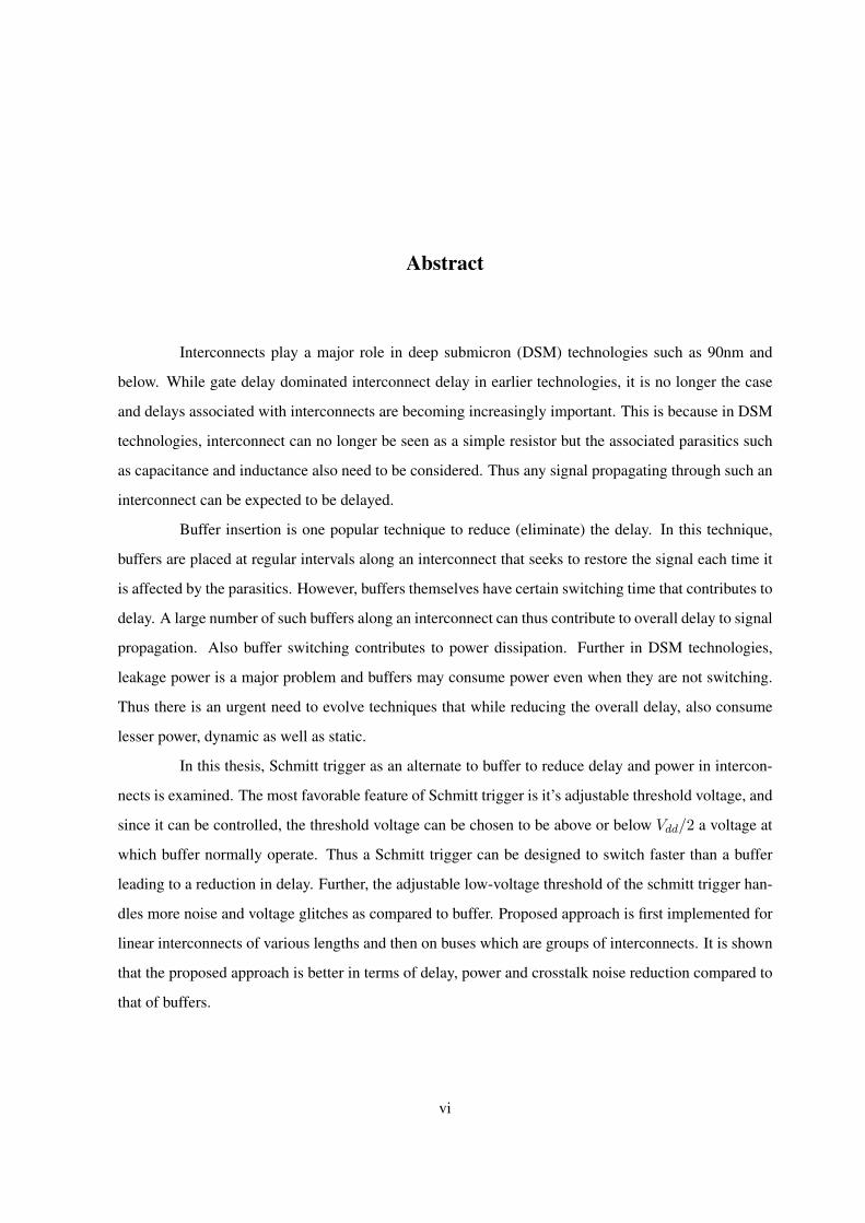
Figure 1.1 The waveform for an 8 bit wide 1 mm long bus at 65nm technology
2
Signals on an interconnect get highly distorted due to propagation delay and coupling effectsof adjacent lines. The effect of this is shown in figure 1.1 for a group of 8 interconnects laid side byside at 65nm technology. This figure depicts the delayed signals on interconnects of length equal to 1mm. There are not only visible propagation delays in each signal but also quite significant presenceof noise glitches due to switching signals on adjacent lines. Hence along with power and delay, noisecancellation is also an important point to be noted while developing the algorithm/technique for bettertransmission.
Reduction of delay and power consumption is the main motivation behind using repeater/bufferinsertion technique. In this technique a large interconnect is broken into smaller pieces and joined withCMOS buffers. For example, assume a long interconnect has 5 units of resistance and 10 units of capac-itance. The total RC delay would be 50 units. However, if five repeaters are inserted within this line tobreak the interconnect into five equal pieces, the RC delay would be 1 x 2 + 1 x 2+ 1 x 2+ 1 x 2 + 1 x 2= 10 units. If the delay of the five repeaters is less than 40 units, then there is a speed benefit to insertingCMOS repeaters. Hence the solution for this problem has been approached in the same manner.
1.3 Literature Survey
The objective of buffer insertion is to find where to insert buffers in the interconnect so thatthe timing requirements are met. Since the propagation (Elmore) delay has a square dependence onthe length of an RC interconnect line, subdividing the line into shorter sections is an effective strategyto reduce the total propagation delay [6]. The interconnect can be subdivided into shorter sections byinserting repeaters, which break the quadratic dependence of the delay on the interconnect length butadd additional parasitic impedances due to the inserted repeaters. Thus, an optimum number and size ofrepeaters exist that minimizes the total propagation delay of the line [6].
Buffer insertion for a single net or interconnect tree is a well-researched problem. Ginneken[9] proposed a time dynamic programming algorithm in 1991 to maximize the slack of the net that has atime complexity of O(n2). Since then, his algorithm has become a classic in this field and a substantialbody of research has developed on the basis of van Ginneken’s algorithm. The work in [14] suggesteda wire segmenting algorithm to be used as a precursor to van Ginneken’s algorithm resulting in fasterrun-time. Lillis et al. [13] extended the framework to minimize buffer cost while satisfying the timingrequirements. Li et al. [15] improved the time bound on van Ginneken’s algorithm to O(nlogn). Theauthors of [16] proved that optimizing the total cost given arbitrary buffer costs is a NP-hard problem,and also suggested techniques to improve the efficiency of Lillis’ algorithm. Previous researchers [10,11, 12] have taken other approaches to solve different variants of the buffer insertion problem like si-multaneous routing, simultaneous gate sizing, and inclusion of slew and signal integrity constraints.
3
In real applications however, the primary objective is to reduce the path delay in combinationalcircuits rather single net delay. Therefore, buffer insertion should be performed at the circuit level ratherthan at the net-level. This calls for efficient algorithms at the circuit level that capitalize on the progressmade by the faster net level buffer insertion algorithms cited above. The motivation of this researchwork is to develop such a circuit level algorithm that works efficiently at net-level.
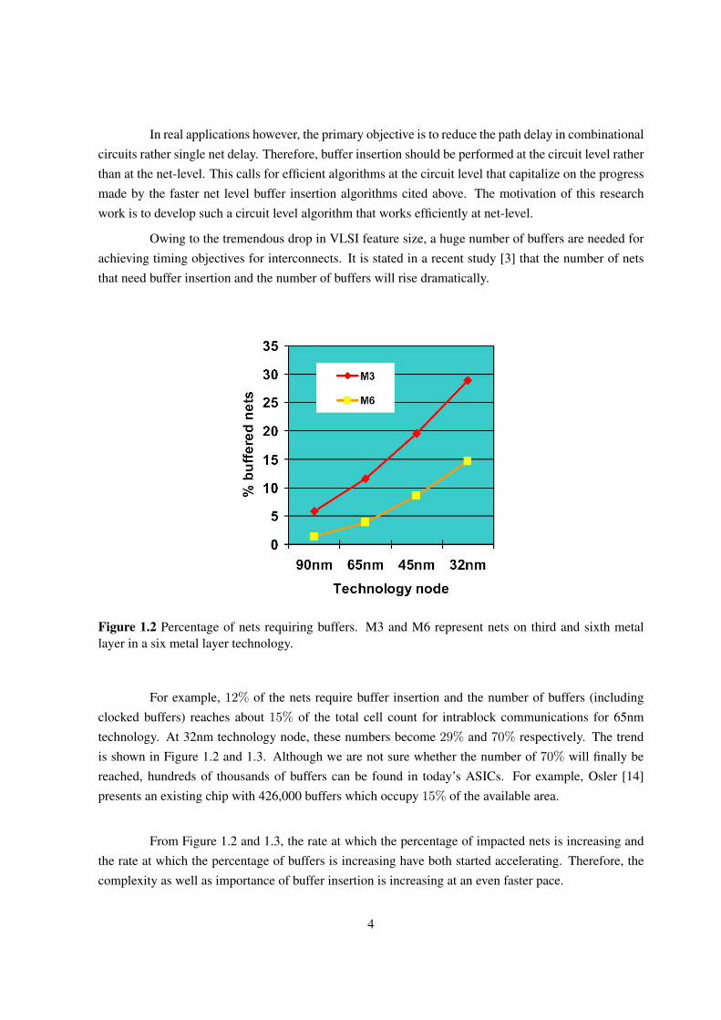
Owing to the tremendous drop in VLSI feature size, a huge number of buffers are needed forachieving timing objectives for interconnects. It is stated in a recent study [3] that the number of netsthat need buffer insertion and the number of buffers will rise dramatically.
Figure 1.2 Percentage of nets requiring buffers. M3 and M6 represent nets on third and sixth metallayer in a six metal layer technology.
For example, 12% of the nets require buffer insertion and the number of buffers (includingclocked buffers) reaches about 15% of the total cell count for intrablock communications for 65nmtechnology. At 32nm technology node, these numbers become 29% and 70% respectively. The trendis shown in Figure 1.2 and 1.3. Although we are not sure whether the number of 70% will finally bereached, hundreds of thousands of buffers can be found in today’s ASICs. For example, Osler [14]presents an existing chip with 426,000 buffers which occupy 15% of the available area.
From Figure 1.2 and 1.3, the rate at which the percentage of impacted nets is increasing andthe rate at which the percentage of buffers is increasing have both started accelerating. Therefore, thecomplexity as well as importance of buffer insertion is increasing at an even faster pace.
4
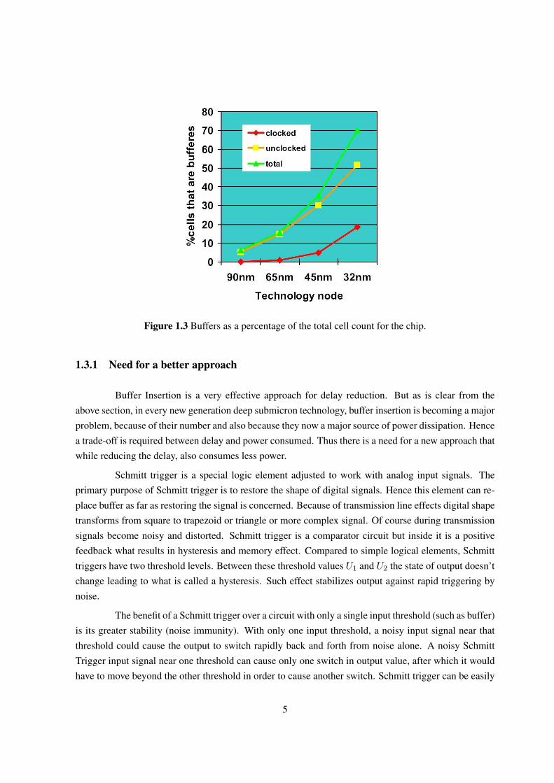
Figure 1.3 Buffers as a percentage of the total cell count for the chip.
1.3.1 Need for a better approach
Buffer Insertion is a very effective approach for delay reduction. But as is clear from theabove section, in every new generation deep submicron technology, buffer insertion is becoming a majorproblem, because of their number and also because they now a major source of power dissipation. Hencea trade-off is required between delay and power consumed. Thus there is a need for a new approach thatwhile reducing the delay, also consumes less power.
Schmitt trigger is a special logic element adjusted to work with analog input signals. Theprimary purpose of Schmitt trigger is to restore the shape of digital signals. Hence this element can re-place buffer as far as restoring the signal is concerned. Because of transmission line effects digital shapetransforms from square to trapezoid or triangle or more complex signal. Of course during transmissionsignals become noisy and distorted. Schmitt trigger is a comparator circuit but inside it is a positivefeedback what results in hysteresis and memory effect. Compared to simple logical elements, Schmitttriggers have two threshold levels. Between these threshold values U1 and U2 the state of output doesn’tchange leading to what is called a hysteresis. Such effect stabilizes output against rapid triggering bynoise.
The benefit of a Schmitt trigger over a circuit with only a single input threshold (such as buffer)is its greater stability (noise immunity). With only one input threshold, a noisy input signal near thatthreshold could cause the output to switch rapidly back and forth from noise alone. A noisy SchmittTrigger input signal near one threshold can cause only one switch in output value, after which it wouldhave to move beyond the other threshold in order to cause another switch. Schmitt trigger can be easily
5
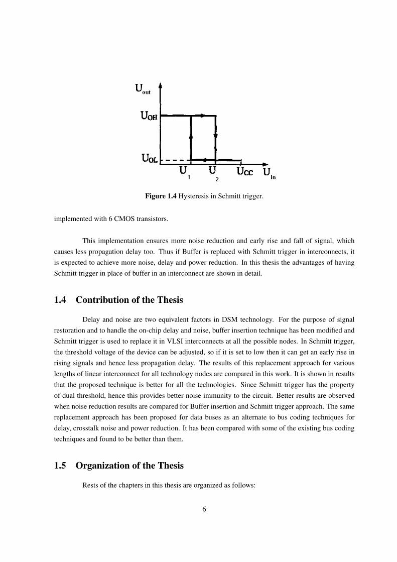
Figure 1.4 Hysteresis in Schmitt trigger.
implemented with 6 CMOS transistors.
This implementation ensures more noise reduction and early rise and fall of signal, whichcauses less propagation delay too. Thus if Buffer is replaced with Schmitt trigger in interconnects, itis expected to achieve more noise, delay and power reduction. In this thesis the advantages of havingSchmitt trigger in place of buffer in an interconnect are shown in detail.
1.4 Contribution of the Thesis
Delay and noise are two equivalent factors in DSM technology. For the purpose of signalrestoration and to handle the on-chip delay and noise, buffer insertion technique has been modified andSchmitt trigger is used to replace it in VLSI interconnects at all the possible nodes. In Schmitt trigger,the threshold voltage of the device can be adjusted, so if it is set to low then it can get an early rise inrising signals and hence less propagation delay. The results of this replacement approach for variouslengths of linear interconnect for all technology nodes are compared in this work. It is shown in resultsthat the proposed technique is better for all the technologies. Since Schmitt trigger has the propertyof dual threshold, hence this provides better noise immunity to the circuit. Better results are observedwhen noise reduction results are compared for Buffer insertion and Schmitt trigger approach. The samereplacement approach has been proposed for data buses as an alternate to bus coding techniques fordelay, crosstalk noise and power reduction. It has been compared with some of the existing bus codingtechniques and found to be better than them.
1.5 Organization of the Thesis
Rests of the chapters in this thesis are organized as follows:
6

• Chapter 2 provides a description of interconnects while explaining the interconnect design criteria,their basic properties and the models to represent them in circuits. Various existing models forinterconnect design are discussed in this chapter. Then it deals with the existing problems ininterconnects and their growing trends with next coming technologies, the possible solutions andeffectiveness of these solutions.
• Chapter 3 gives an introduction to conventional buffer insertion technique for the purpose of signalrestoration and delay reduction. Benefits of buffer insertion in linear interconnect and their use indelay and noise reduction are explained along with various buffer insertion existing in literature.This chapter provides the understanding of basics about propagation delay, power dissipation anddesign criteria. It is also shown how buffer insertion is becoming a bulky technique and goingto consume more and more resources in incoming technologies. Limitations of buffer insertiontechnology in terms of area and power consumption are discussed in the end.
• Chapter 4 introduces Schmitt trigger. History, invention and basic circuit implementation ofSchmitt trigger are discussed in early sections of the chapter. Implementation and working ofSchmitt trigger is discussed in detail. CMOS Schmitt triggers are mentioned in the later sectionsof the chapter. Benefits of Schmitt trigger over buffer for the purpose of signal restoration anddelay reduction is discussed in the end.
• Chapter 5 contains the simulation results for all types of interconnects, namely local, intermediateand global, with existing as well as proposed approaches. First of all the problems in Intercon-nects are simulated and then the conventional solution of buffer insertion. Simulations are donein for 180nm to 65nm nodes using PTM parameters with H-Spice tool. Simulations are based onthe following criteria:Propagation DelayNoise reductionPower reduction
• Chapter 6 draws conclusions of the thesis.
7
Chapter 2
Introduction to Interconnects
Due to the importance of interconnects in current and future ICs, significant research has beenpublished over the past several decades, covering different areas such as parasitic extraction, intercon-nect models, and interconnect design methodologies.
In this chapter, a brief review of the background of on-chip electrical interconnect is provided.In Section 2.1, a typical design flow for application-specific integrated circuits (ASIC) is described.Challenges in DSM technologies due to interconnect dominant behavior are discussed. In Section2.2, different design criteria that need to be considered during the interconnect design procedure aredescribed. The impedance characteristics of interconnect are presented in Section 2.3; specially, theresistance, capacitance, and inductance. Interconnect models and design methodologies are reviewed inSections 2.4 and 2.5, respectively. Finally, some conclusions are offered in Section 2.6.
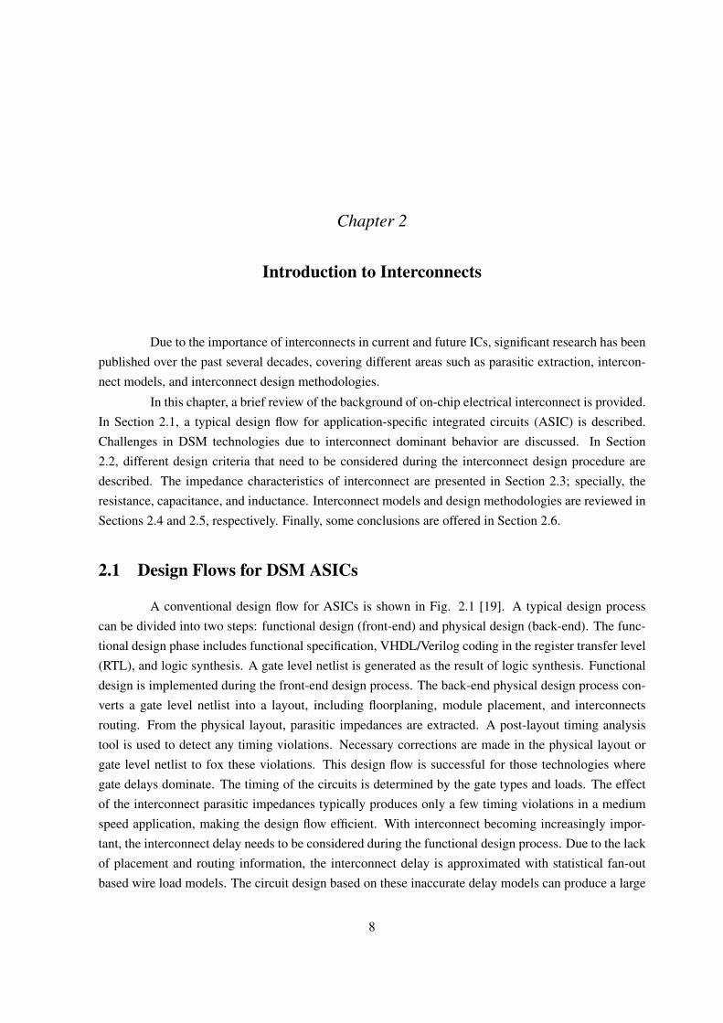
2.1 Design Flows for DSM ASICs
A conventional design flow for ASICs is shown in Fig. 2.1 [19]. A typical design processcan be divided into two steps: functional design (front-end) and physical design (back-end). The func-tional design phase includes functional specification, VHDL/Verilog coding in the register transfer level(RTL), and logic synthesis. A gate level netlist is generated as the result of logic synthesis. Functionaldesign is implemented during the front-end design process. The back-end physical design process con-verts a gate level netlist into a layout, including floorplaning, module placement, and interconnectsrouting. From the physical layout, parasitic impedances are extracted. A post-layout timing analysistool is used to detect any timing violations. Necessary corrections are made in the physical layout orgate level netlist to fox these violations. This design flow is successful for those technologies wheregate delays dominate. The timing of the circuits is determined by the gate types and loads. The effectof the interconnect parasitic impedances typically produces only a few timing violations in a mediumspeed application, making the design flow efficient. With interconnect becoming increasingly impor-tant, the interconnect delay needs to be considered during the functional design process. Due to the lackof placement and routing information, the interconnect delay is approximated with statistical fan-outbased wire load models. The circuit design based on these inaccurate delay models can produce a large
8
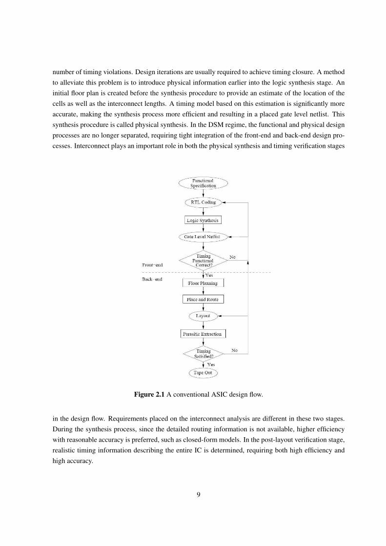
number of timing violations. Design iterations are usually required to achieve timing closure. A methodto alleviate this problem is to introduce physical information earlier into the logic synthesis stage. Aninitial floor plan is created before the synthesis procedure to provide an estimate of the location of thecells as well as the interconnect lengths. A timing model based on this estimation is significantly moreaccurate, making the synthesis process more efficient and resulting in a placed gate level netlist. Thissynthesis procedure is called physical synthesis. In the DSM regime, the functional and physical designprocesses are no longer separated, requiring tight integration of the front-end and back-end design pro-cesses. Interconnect plays an important role in both the physical synthesis and timing verification stages
Figure 2.1 A conventional ASIC design flow.
in the design flow. Requirements placed on the interconnect analysis are different in these two stages.During the synthesis process, since the detailed routing information is not available, higher efficiencywith reasonable accuracy is preferred, such as closed-form models. In the post-layout verification stage,realistic timing information describing the entire IC is determined, requiring both high efficiency andhigh accuracy.
9
2.2 Interconnect Design Criteria
Since interconnect has become a dominant issue in high performance ICs, the focus of thecircuit design process has shifted from logic optimization to interconnect optimization. Multiple criteriashould be considered during the interconnect design process, such as delay, power dissipation, noise,bandwidth, and physical area. These criteria are individually discussed in the following subsections.
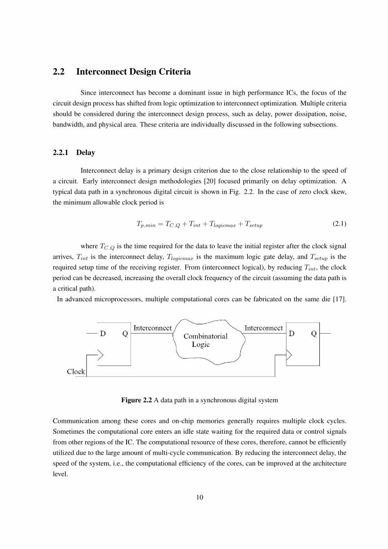
2.2.1 Delay
Interconnect delay is a primary design criterion due to the close relationship to the speed ofa circuit. Early interconnect design methodologies [20] focused primarily on delay optimization. Atypical data path in a synchronous digital circuit is shown in Fig. 2.2. In the case of zero clock skew,the minimum allowable clock period is
Tp min = TC Q + Tint + Tlogicmax + Tsetup (2.1)
where TC Q is the time required for the data to leave the initial register after the clock signalarrives, Tint is the interconnect delay, Tlogicmax is the maximum logic gate delay, and Tsetup is therequired setup time of the receiving register. From (interconnect logical), by reducing Tint, the clockperiod can be decreased, increasing the overall clock frequency of the circuit (assuming the data path isa critical path).
In advanced microprocessors, multiple computational cores can be fabricated on the same die [17].
Figure 2.2 A data path in a synchronous digital system
Communication among these cores and on-chip memories generally requires multiple clock cycles.Sometimes the computational core enters an idle state waiting for the required data or control signalsfrom other regions of the IC. The computational resource of these cores, therefore, cannot be efficientlyutilized due to the large amount of multi-cycle communication. By reducing the interconnect delay, thespeed of the system, i.e., the computational efficiency of the cores, can be improved at the architecturelevel.
10
2.2.2 Power Dissipation
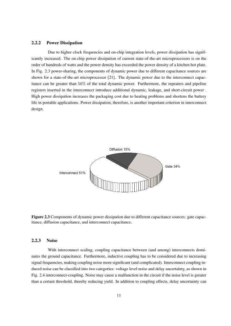
Due to higher clock frequencies and on-chip integration levels, power dissipation has signif-icantly increased. The on-chip power dissipation of current state-of-the-art microprocessors is on theorder of hundreds of watts and the power density has exceeded the power density of a kitchen hot plate.In Fig. 2.3 power-sharing, the components of dynamic power due to different capacitance sources areshown for a state-of-the-art microprocessor [21]. The dynamic power due to the interconnect capac-itance can be greater than 50% of the total dynamic power. Furthermore, the repeaters and pipelineregisters inserted in the interconnect introduce additional dynamic, leakage, and short-circuit power .High power dissipation increases the packaging cost due to heating problems and shortens the batterylife in portable applications. Power dissipation, therefore, is another important criterion in interconnectdesign.
Figure 2.3 Components of dynamic power dissipation due to different capacitance sources: gate capac-itance, diffusion capacitance, and interconnect capacitance.
2.2.3 Noise
With interconnect scaling, coupling capacitance between (and among) interconnects domi-nates the ground capacitance. Furthermore, inductive coupling has to be considered due to increasingsignal frequencies, making coupling noise more significant (and complicated). Interconnect coupling in-duced noise can be classified into two categories: voltage level noise and delay uncertainty, as shown inFig. 2.4 interconnect-coupling. Noise may cause a malfunction in the circuit if the noise level is greaterthan a certain threshold, thereby reducing yield. In addition to coupling effects, delay uncertainty can
11
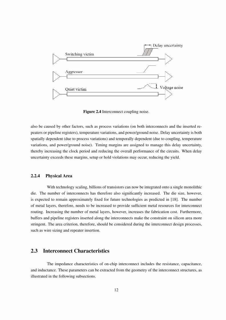
Figure 2.4 Interconnect coupling noise.
also be caused by other factors, such as process variations (on both interconnects and the inserted re-peaters or pipeline registers), temperature variations, and power/ground noise. Delay uncertainty is bothspatially dependent (due to process variations) and temporally dependent (due to coupling, temperaturevariations, and power/ground noise). Timing margins are assigned to manage this delay uncertainty,thereby increasing the clock period and reducing the overall performance of the circuits. When delayuncertainty exceeds these margins, setup or hold violations may occur, reducing the yield.
2.2.4 Physical Area
With technology scaling, billions of transistors can now be integrated onto a single monolithicdie. The number of interconnects has therefore also significantly increased. The die size, however,is expected to remain approximately fixed for future technologies as predicted in [18]. The numberof metal layers, therefore, needs to be increased to provide sufficient metal resources for interconnectrouting. Increasing the number of metal layers, however, increases the fabrication cost. Furthermore,buffers and pipeline registers inserted along the interconnects make the constraint on silicon area morestringent. The area criterion, therefore, should be considered during the interconnect design processes,such as wire sizing and repeater insertion.
2.3 Interconnect Characteristics
The impedance characteristics of on-chip interconnect includes the resistance, capacitance,and inductance. These parameters can be extracted from the geometry of the interconnect structures, asillustrated in the following subsections.
12
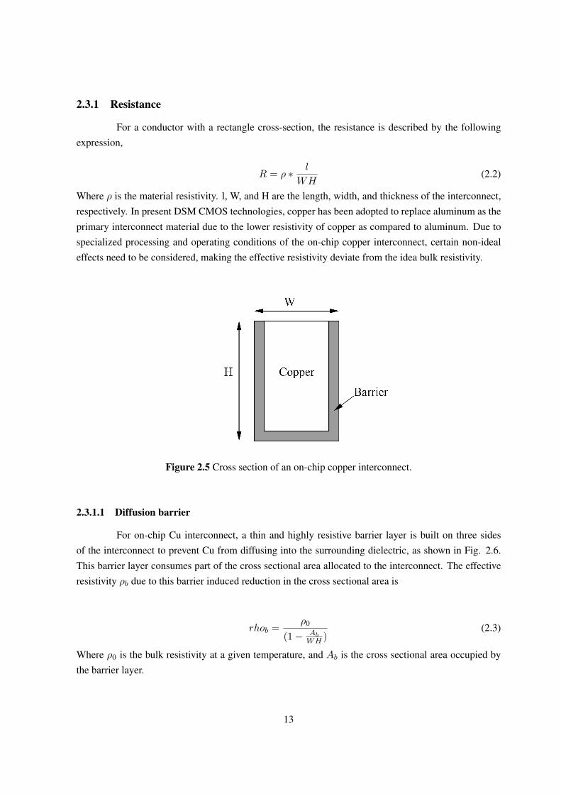
2.3.1 Resistance
For a conductor with a rectangle cross-section, the resistance is described by the followingexpression,
R = ρ ∗ l
WH(2.2)
Where ρ is the material resistivity. l, W, and H are the length, width, and thickness of the interconnect,respectively. In present DSM CMOS technologies, copper has been adopted to replace aluminum as theprimary interconnect material due to the lower resistivity of copper as compared to aluminum. Due tospecialized processing and operating conditions of the on-chip copper interconnect, certain non-idealeffects need to be considered, making the effective resistivity deviate from the idea bulk resistivity.
Figure 2.5 Cross section of an on-chip copper interconnect.
2.3.1.1 Diffusion barrier
For on-chip Cu interconnect, a thin and highly resistive barrier layer is built on three sidesof the interconnect to prevent Cu from diffusing into the surrounding dielectric, as shown in Fig. 2.6.This barrier layer consumes part of the cross sectional area allocated to the interconnect. The effectiveresistivity ρb due to this barrier induced reduction in the cross sectional area is
rhob =ρ0
(1− AbWH )
(2.3)
Where ρ0 is the bulk resistivity at a given temperature, and Ab is the cross sectional area occupied bythe barrier layer.
13
2.3.1.2 Surface and grain boundary scattering
When the dimensions of the interconnect are scaled deep into the DSM regime, the resistivityof the interconnect increases as the wire dimensions shrink. This behavior is due to surface and grainboundary scattering [22], as illustrated in Fig. 2.7.
The electron mean-free path λ of copper is 42.1 nm at 0 degree Celsius. [22]. When anydimension of the wire shrinks to the order of λ, the electrons will experience more collisions at thesurface, increasing the effective resistivity. A typical value of ρ for copper is 0.47 [22]. Note that in(2.6) and (2.7), only one dimension (thin film structure) surface scattering is considered. For thin wireswith two-dimensional surface scattering effect, the effective resistivity is larger. A reduced k is used in[24] to consider this two-dimensional surface scattering effect.
2.3.1.3 Temperature effect
The resistivity of copper increases approximately linearly with temperature and can be char-acterized as
ρt = ρ0(1 + βδt) (2.4)
where β is the temperature coefficient of resistivity (TCR) and δ T is the difference in temper-ature from a reference temperature. Since the electron mean-free path λ will decrease with increasingtemperature, the k will be resulting in a smaller ratio of ρs/ρ0. The TCR for thin-film interconnect,therefore, is smaller than that of bulk Cu [23].
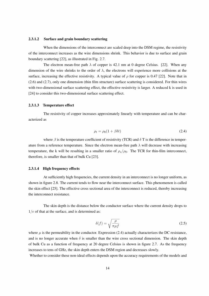
2.3.1.4 High frequency effects
At sufficiently high frequencies, the current density in an interconnect is no longer uniform, asshown in figure 2.8. The current tends to flow near the interconnect surface. This phenomenon is calledthe skin effect [25]. The effective cross sectional area of the interconnect is reduced, thereby increasingthe interconnect resistance.
The skin depth is the distance below the conductor surface where the current density drops to1/e of that at the surface, and is determined as:
δ(f) =√
ρ
πµf(2.5)
where µ is the permeability in the conductor. Expression (2.4) actually characterizes the DC resistance,and is no longer accurate when δ is smaller than the wire cross sectional dimension. The skin depthof bulk Cu as a function of frequency at 20 degree Celsius is shown in figure 2.7. As the frequencyincreases to tens of GHz, the skin depth enters the DSM region and decreases slowly.Whether to consider these non-ideal effects depends upon the accuracy requirements of the models and
14
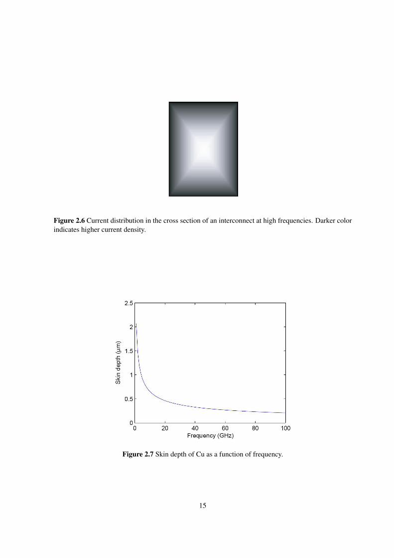
Figure 2.6 Current distribution in the cross section of an interconnect at high frequencies. Darker colorindicates higher current density.
Figure 2.7 Skin depth of Cu as a function of frequency.
15
the operating regime of the circuits. Often more than one effect needs to be simultaneously considered.For example, the skin effect and surface scattering effect when simultaneously considered is known asthe anomalous skin effect (ASE).
2.3.2 Capacitance
Since interconnect delay dominates gate delay in the DSM regime, the requirement on theaccuracy of parasitic extraction of the interconnect impedances increases. 2-D or 3-D extraction isgenerally required. A 3-D field solver, such as FastCap [26],can provide accurate capacitance results,however, with large timing and memory requirements. With increasing integration, the number andgeometric complexity of the on-chip interconnects drastically increases. It is, therefore, not practical toapply a field solver to an entire IC. Modern 3-D on-chip capacitance extraction can be divided into threesteps. Initially, test patterns are measured or simulated with a 2-D or 3-D field solver. The generateddata are used to derive closed-form formulae or to build look-up tables. The geometric parameters of theinterconnects are extracted next. Finally, the geometric parameters are matched to the test patterns, andthe capacitance values are obtained through formulae or look-up tables. Due to the short-range natureof electrostatic interaction, only the nearest neighbors are considered during the process of capacitanceextraction. The capacitance matrices, therefore, are fairly sparse. Interconnect capacitance is composedof two components, the capacitance between the interconnect and adjacent metal layers or substrate Cg,and the coupling capacitance between neighboring interconnects in the same layer Cc.Cc is expectedto dominate Cg in the DSM regime due to the increasing aspect ratio and decreasing wire spacing. Inearly stage interconnect design and analysis, adjacent layers are generally treated as a ground plane forcapacitance extraction. By numerical fitting, closed-form capacitance expressions have been derived forparallel lines above one ground plane or between two ground planes in [27, 28].
2.3.3 Inductance
As compared with resistance and capacitance, the interconnect inductance is significantlymore difficult to extract. One reason for this difficulty is due to the loop-based inductance definition,
Lij =ψij
Ij(2.6)
Where ψij is the magnetic flux in loop i induced by the current Ij in loop j. To form a loop,the current return paths need to be identified. The current distribution in a circuit, however, a prioridepends on the interconnect characteristics. The effect of inductance in wide global interconnects in topmetal layers is more significant than that of local interconnects in lower metal layers. Since the wiresin adjacent layers are generally orthogonal, adjacent layers can no longer be treated as a ground planeas in capacitance extraction. Another reason for the difficulty in inductance extraction is due to longrange inductive coupling effects. Artificially restricting the inductance extraction to nearby geometriesnot only introduces inaccuracy but may also result in unstable models. The pattern matching method
16

used for capacitance extraction, therefore, can not be used for inductance extraction due to the complexgeometries surrounding the wire.
2.3.3.1 Partial inductance
One way to avoid determining a priori the current return path is to use the concept of partialinductance [28]. In determining the partial inductance, the flux area extends from the conductor toinfinity. The loop inductance of a closed loop can be uniquely determined by the partial self-inductanceof each segment of the loop and the partial mutual inductance between any pair of those segments. Thepartial inductance is used in partial element equivalent circuit (PEEC) models, which can be used toaccurately simulate a circuit. Partial inductance nonlinearly depends upon the interconnect length. Thisbehavior is the result of inductive coupling among different segments of the same line [25]. For a loopformed by two closely placed parallel interconnects (where the length of the loop is more than ten timeslonger than the loop width), the loop inductance depends linearly on the length of the loop. Note that theinductance of a wire not forming a closed loop has no physical meaning [28]. When applying the conceptof partial inductance in circuit models, all of the wires that form the current loops should be included,e.g., the reference ground lines. The current return paths are determined from circuit simulation. ThePEEC model generally results in huge and dense inductance matrices, increasing the computationalcomplexity of the simulation. Various methods have been presented to sparsify the inductance matrices[29], such as the shell technique, the halo technique, and the K matrix technique.
2.3.3.2 Loop-based inductance
As an alternative to the PEEC model, a loop-based inductance model is preferred in well-designed interconnect structures, such as shielded buses and clock distribution networks. In early designstages, a good assumption regarding the current return path is the nearby power/ground networks, sincethese tracks are generally wide with low resistive impedance. ’FastHenry’ is a commonly used numer-ical tool for extracting the partial or loop inductance of simple interconnects structures. By estimatingthe distribution of the return current, more accurate loop-based inductance models have been developed[30, 31].
2.3.3.3 High frequency effects
Inductance is also a function of frequency due to the variation of the current distribution withfrequency. In addition to the skin effect mentioned in Subsection 2.3.1, the current distribution insidea conductor also changes with frequency due to the proximity effect [25]. The proximity effect in twoparallel interconnects is illustrated in figure 2.8. If the current in these two wires flows in oppositedirections, the currents concentrate towards each other, as shown in Fig. 2.10(a); otherwise, the twocurrents shift away from each other, as shown in Fig. 2.10(b). Both the skin effect and the proximityeffect are essentially due to the same mechanism. The current tends to concentrate closer to the current
17
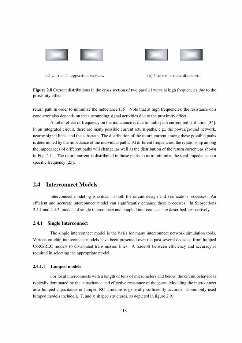
Figure 2.8 Current distributions in the cross section of two parallel wires at high frequencies due to theproximity effect.
return path in order to minimize the inductance [35]. Note that at high frequencies, the resistance of aconductor also depends on the surrounding signal activities due to the proximity effect.
Another effect of frequency on the inductance is due to multi-path current redistribution [34].In an integrated circuit, there are many possible current return paths, e.g., the power/ground network,nearby signal lines, and the substrate. The distribution of the return current among these possible pathsis determined by the impedance of the individual paths. At different frequencies, the relationship amongthe impedances of different paths will change, as well as the distribution of the return current, as shownin Fig. 2.11. The return current is distributed in those paths so as to minimize the total impedance at aspecific frequency [25].
2.4 Interconnect Models
Interconnect modeling is critical in both the circuit design and verification processes. Anefficient and accurate interconnect model can significantly enhance these processes. In Subsections2.4.1 and 2.4.2, models of single interconnect and coupled interconnects are described, respectively.
2.4.1 Single Interconnect
The single interconnect model is the basis for many interconnect network simulation tools.Various on-chip interconnect models have been presented over the past several decades, from lumpedC/RC/RLC models to distributed transmission lines. A tradeoff between efficiency and accuracy isrequired in selecting the appropriate model.
2.4.1.1 Lumped models
For local interconnects with a length of tens of micrometers and below, the circuit behavior istypically dominated by the capacitance and effective resistance of the gates. Modeling the interconnectas a lumped capacitance or lumped RC structure is generally sufficiently accurate. Commonly usedlumped models include L, T, and π shaped structures, as depicted in figure 2.9.
18
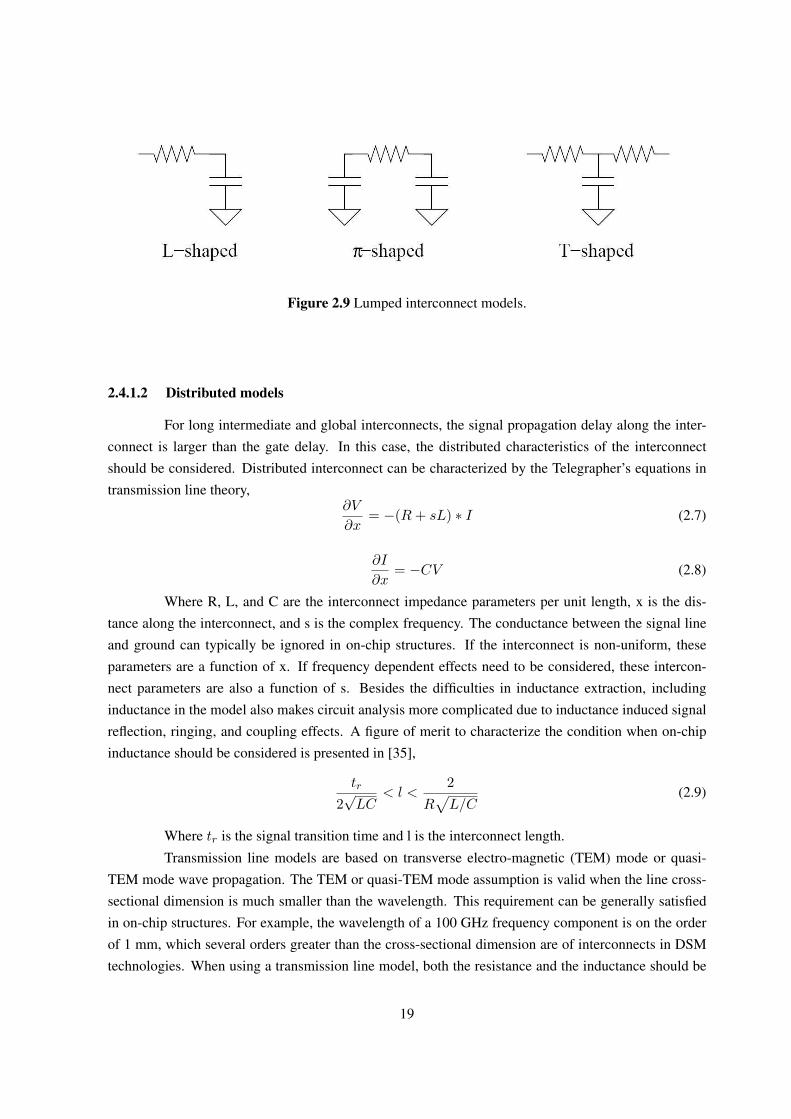
Figure 2.9 Lumped interconnect models.
2.4.1.2 Distributed models
For long intermediate and global interconnects, the signal propagation delay along the inter-connect is larger than the gate delay. In this case, the distributed characteristics of the interconnectshould be considered. Distributed interconnect can be characterized by the Telegrapher’s equations intransmission line theory,
∂V
∂x= −(R + sL) ∗ I (2.7)
∂I
∂x= −CV (2.8)
Where R, L, and C are the interconnect impedance parameters per unit length, x is the dis-tance along the interconnect, and s is the complex frequency. The conductance between the signal lineand ground can typically be ignored in on-chip structures. If the interconnect is non-uniform, theseparameters are a function of x. If frequency dependent effects need to be considered, these intercon-nect parameters are also a function of s. Besides the difficulties in inductance extraction, includinginductance in the model also makes circuit analysis more complicated due to inductance induced signalreflection, ringing, and coupling effects. A figure of merit to characterize the condition when on-chipinductance should be considered is presented in [35],
tr
2√
LC< l <
2R
√L/C
(2.9)
Where tr is the signal transition time and l is the interconnect length.
Transmission line models are based on transverse electro-magnetic (TEM) mode or quasi-TEM mode wave propagation. The TEM or quasi-TEM mode assumption is valid when the line cross-sectional dimension is much smaller than the wavelength. This requirement can be generally satisfiedin on-chip structures. For example, the wavelength of a 100 GHz frequency component is on the orderof 1 mm, which several orders greater than the cross-sectional dimension are of interconnects in DSMtechnologies. When using a transmission line model, both the resistance and the inductance should be
19
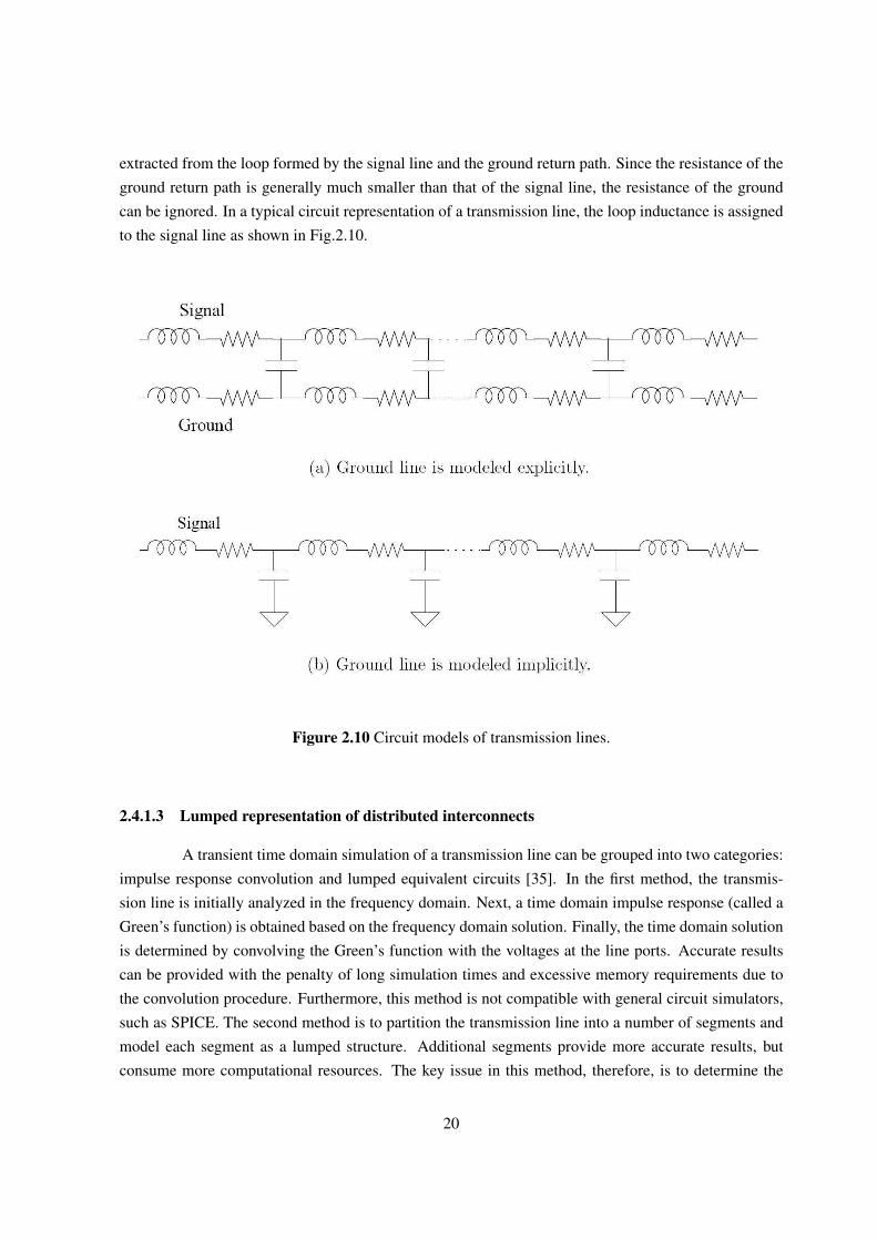
extracted from the loop formed by the signal line and the ground return path. Since the resistance of theground return path is generally much smaller than that of the signal line, the resistance of the groundcan be ignored. In a typical circuit representation of a transmission line, the loop inductance is assignedto the signal line as shown in Fig.2.10.
Figure 2.10 Circuit models of transmission lines.
2.4.1.3 Lumped representation of distributed interconnects
A transient time domain simulation of a transmission line can be grouped into two categories:impulse response convolution and lumped equivalent circuits [35]. In the first method, the transmis-sion line is initially analyzed in the frequency domain. Next, a time domain impulse response (called aGreen’s function) is obtained based on the frequency domain solution. Finally, the time domain solutionis determined by convolving the Green’s function with the voltages at the line ports. Accurate resultscan be provided with the penalty of long simulation times and excessive memory requirements due tothe convolution procedure. Furthermore, this method is not compatible with general circuit simulators,such as SPICE. The second method is to partition the transmission line into a number of segments andmodel each segment as a lumped structure. Additional segments provide more accurate results, butconsume more computational resources. The key issue in this method, therefore, is to determine the
20

appropriate number of segments.
Using lumped models to represent a distributed transmission line introduces inaccuracy whenevaluating circuits that operate at high frequencies. The highest frequency of interest, therefore, shouldbe determined in order to evaluate the maximum error induced by using lumped models. The frequencydomain representation of a normalized saturated ramp signal with rise time tr is
Vr(s) =(1− str)(tr ∗ s2)
(2.10)
2.4.1.4 Modeling frequency dependent effects
After partitioning a distributed line into lumped segments, frequency dependent effects can bemodeled in each segment by a ladder structure of frequency independent lumped RL elements, as shownin figure 2.11. Additional ladder stages provide higher accuracy when operating at high frequencies.Two stages are used in [30] and three stages are used in [31, 36]. The value of the circuit elements canbe obtained by matching the impedance of the model to the extracted impedance at different frequencies.
Figure 2.11 Modeling frequency dependent impedance with lumped elements.
2.4.2 Parallel Coupled Interconnects
Modeling parallel coupled interconnects draws special attention in the circuit design processdue to the commonly used bus structure [37]. A general solution for coupled multiconductor systemsis composed of two steps, decoupling the systems into independent interconnects, followed by applying
21
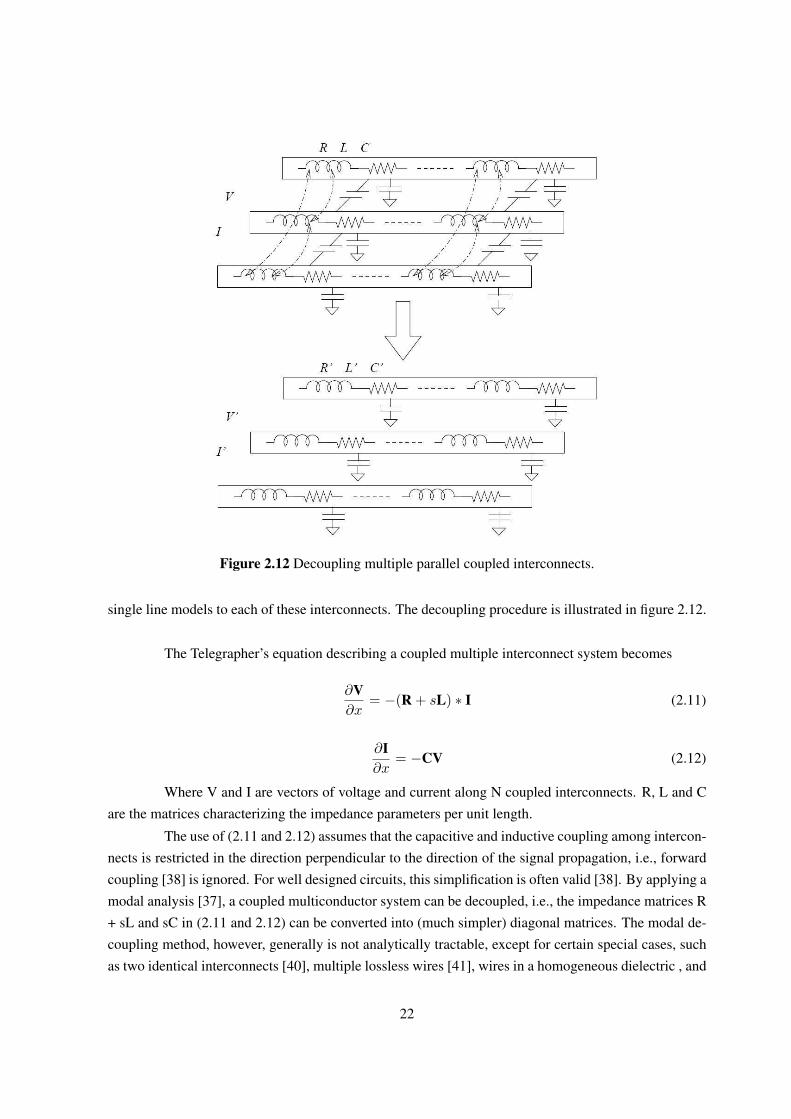
Figure 2.12 Decoupling multiple parallel coupled interconnects.
single line models to each of these interconnects. The decoupling procedure is illustrated in figure 2.12.
The Telegrapher’s equation describing a coupled multiple interconnect system becomes
∂V∂x
= −(R + sL) ∗ I (2.11)
∂I∂x
= −CV (2.12)
Where V and I are vectors of voltage and current along N coupled interconnects. R, L and Care the matrices characterizing the impedance parameters per unit length.
The use of (2.11 and 2.12) assumes that the capacitive and inductive coupling among intercon-nects is restricted in the direction perpendicular to the direction of the signal propagation, i.e., forwardcoupling [38] is ignored. For well designed circuits, this simplification is often valid [38]. By applying amodal analysis [37], a coupled multiconductor system can be decoupled, i.e., the impedance matrices R+ sL and sC in (2.11 and 2.12) can be converted into (much simpler) diagonal matrices. The modal de-coupling method, however, generally is not analytically tractable, except for certain special cases, suchas two identical interconnects [40], multiple lossless wires [41], wires in a homogeneous dielectric , and
22
wires only coupled to direct neighbors. In general, the computational complexity required to decouplea large number of coupled lossy interconnects with a modal analysis is high.
2.5 Design Methodologies for Interconnect
Since interconnect plays an important role in ICs, interconnect design methodologies havebeen developed at different levels to satisfy specific performance requirements. In Subsection 2.5.1,interconnect topology optimization methods are discussed, where interconnect trees are constructed.Wire geometry optimization methods are reviewed in Subsection 2.5.2. Circuit level interconnect designmethodologies are described in Subsections 2.5.3, 2.5.4, and 2.5.5, including buffer insertion, shieldingtechniques, and net-ordering/wire swizzling, respectively.
2.5.1 Constructing an Interconnect Tree
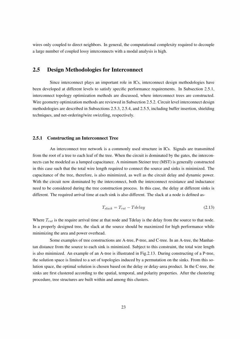
An interconnect tree network is a commonly used structure in ICs. Signals are transmittedfrom the root of a tree to each leaf of the tree. When the circuit is dominated by the gates, the intercon-nects can be modeled as a lumped capacitance. A minimum Steiner tree (MST) is generally constructedin this case such that the total wire length required to connect the source and sinks is minimized. Thecapacitance of the tree, therefore, is also minimized, as well as the circuit delay and dynamic power.With the circuit now dominated by the interconnect, both the interconnect resistance and inductanceneed to be considered during the tree construction process. In this case, the delay at different sinks isdifferent. The required arrival time at each sink is also different. The slack at a node is defined as-
Tslack = Trat − Tdelay (2.13)
Where Trat is the require arrival time at that node and Tdelay is the delay from the source to that node.In a properly designed tree, the slack at the source should be maximized for high performance whileminimizing the area and power overhead.
Some examples of tree constructions are A-tree, P-tree, and C-tree. In an A-tree, the Manhat-tan distance from the source to each sink is minimized. Subject to this constraint, the total wire lengthis also minimized. An example of an A-tree is illustrated in Fig.2.13. During constructing of a P-tree,the solution space is limited to a set of topologies induced by a permutation on the sinks. From this so-lution space, the optimal solution is chosen based on the delay or delay-area product. In the C-tree, thesinks are first clustered according to the spatial, temporal, and polarity properties. After the clusteringprocedure, tree structures are built within and among this clusters.
23
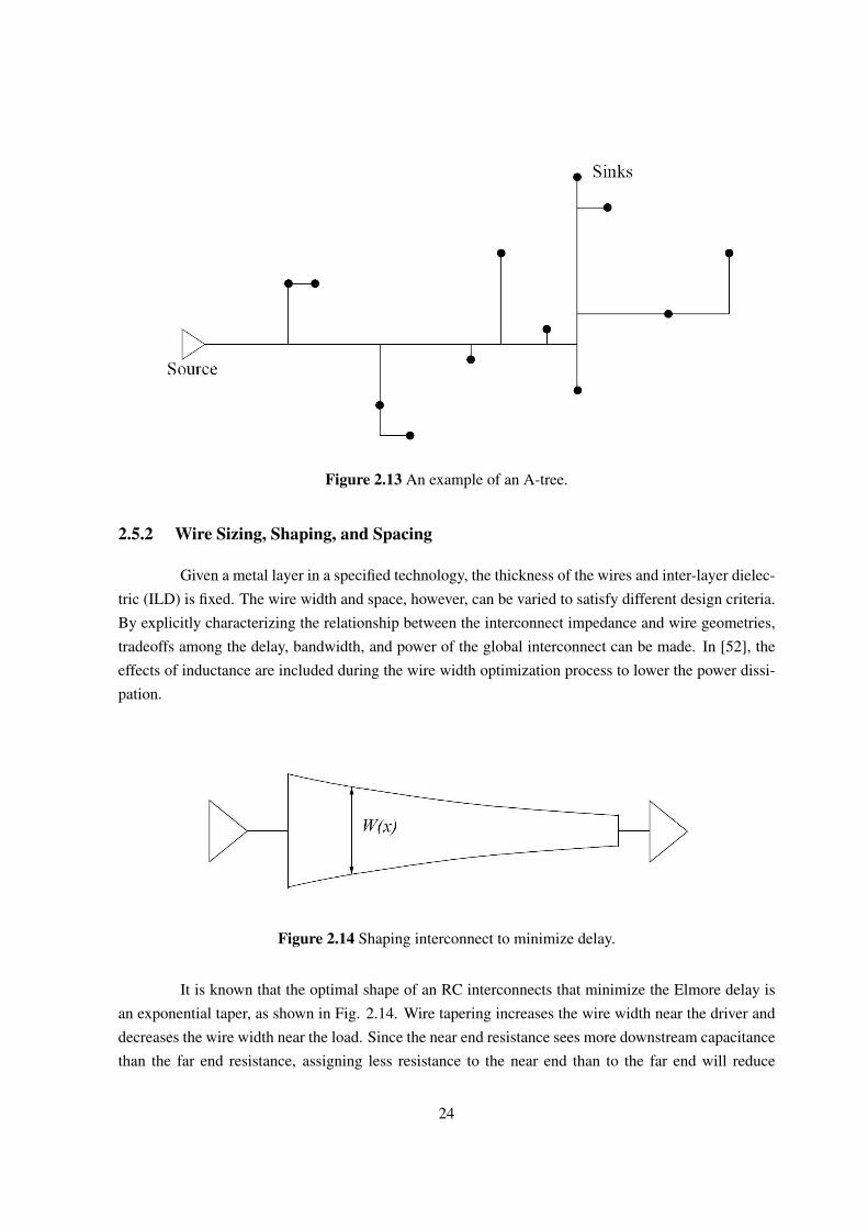
Figure 2.13 An example of an A-tree.
2.5.2 Wire Sizing, Shaping, and Spacing
Given a metal layer in a specified technology, the thickness of the wires and inter-layer dielec-tric (ILD) is fixed. The wire width and space, however, can be varied to satisfy different design criteria.By explicitly characterizing the relationship between the interconnect impedance and wire geometries,tradeoffs among the delay, bandwidth, and power of the global interconnect can be made. In [52], theeffects of inductance are included during the wire width optimization process to lower the power dissi-pation.
Figure 2.14 Shaping interconnect to minimize delay.
It is known that the optimal shape of an RC interconnects that minimize the Elmore delay isan exponential taper, as shown in Fig. 2.14. Wire tapering increases the wire width near the driver anddecreases the wire width near the load. Since the near end resistance sees more downstream capacitancethan the far end resistance, assigning less resistance to the near end than to the far end will reduce
24
the total RC delay. In [44], the optimal shape of an RC interconnect is also shown to be exponential.Exponential shaping, however, is more difficult to implement than uniformly sized wires.
2.5.3 Repeater Insertion
The delay of an RC interconnect is 0:377 RCl2 , which is proportional to the square of thewire length l. By splitting the interconnect into k segments with repeaters, the interconnect delay termis reduced to 0:377 RCl2/k. These repeaters, however, introduce additional gate delay. The optimalnumber and size of the repeaters can be determined to achieve the minimum delay [20]. As signalspropagate along the interconnect, sharper transition edges are regenerated by the repeaters, increasingthe bandwidth of the interconnect. By dividing the interconnect into segments, the coupling betweeninterconnects is also reduced due to the shorter length of coupling between neighboring lines. Insertingrepeaters in long interconnects, however, introduces an area and power penalty. A tradeoff among dif-ferent design criteria is, therefore, required for an effecient repeater insertion methodology.
Figure 2.15 Staggering repeaters to reduce the worst case delay and crosstalk noise.
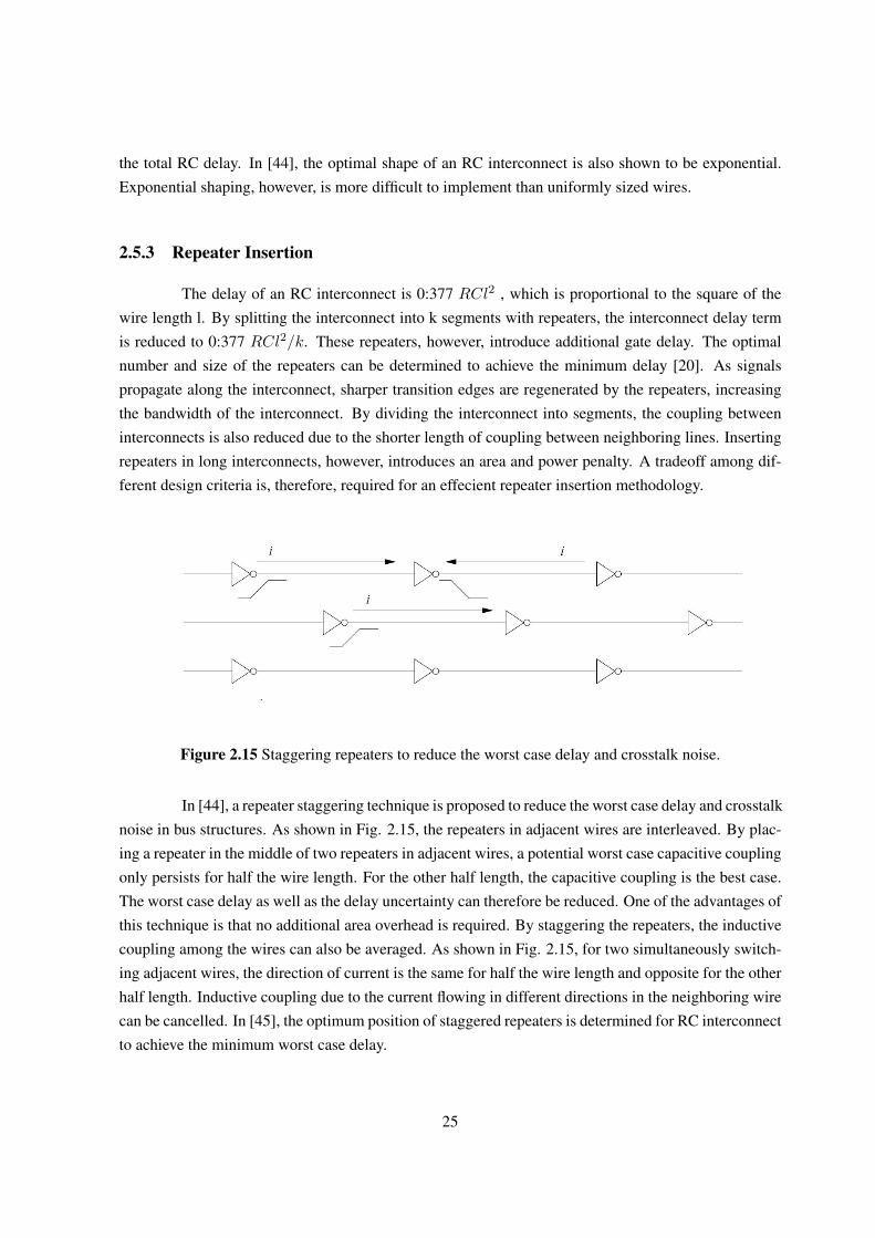
In [44], a repeater staggering technique is proposed to reduce the worst case delay and crosstalknoise in bus structures. As shown in Fig. 2.15, the repeaters in adjacent wires are interleaved. By plac-ing a repeater in the middle of two repeaters in adjacent wires, a potential worst case capacitive couplingonly persists for half the wire length. For the other half length, the capacitive coupling is the best case.The worst case delay as well as the delay uncertainty can therefore be reduced. One of the advantages ofthis technique is that no additional area overhead is required. By staggering the repeaters, the inductivecoupling among the wires can also be averaged. As shown in Fig. 2.15, for two simultaneously switch-ing adjacent wires, the direction of current is the same for half the wire length and opposite for the otherhalf length. Inductive coupling due to the current flowing in different directions in the neighboring wirecan be cancelled. In [45], the optimum position of staggered repeaters is determined for RC interconnectto achieve the minimum worst case delay.
25
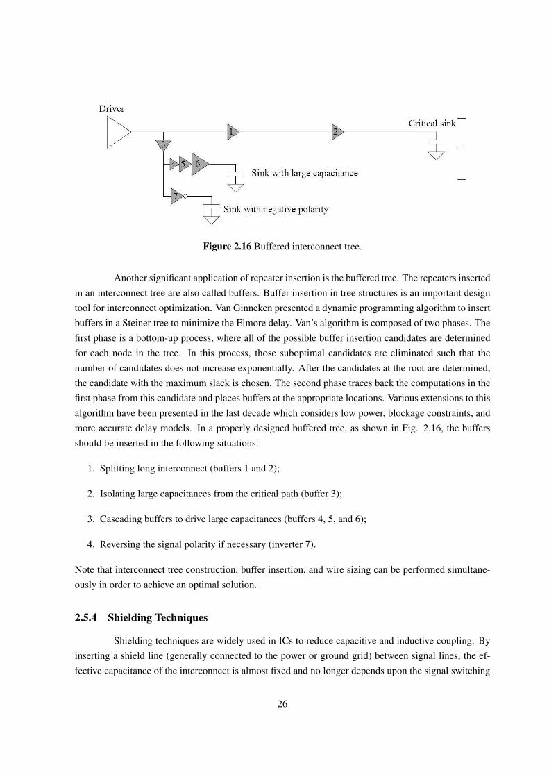
Figure 2.16 Buffered interconnect tree.
Another significant application of repeater insertion is the buffered tree. The repeaters insertedin an interconnect tree are also called buffers. Buffer insertion in tree structures is an important designtool for interconnect optimization. Van Ginneken presented a dynamic programming algorithm to insertbuffers in a Steiner tree to minimize the Elmore delay. Van’s algorithm is composed of two phases. Thefirst phase is a bottom-up process, where all of the possible buffer insertion candidates are determinedfor each node in the tree. In this process, those suboptimal candidates are eliminated such that thenumber of candidates does not increase exponentially. After the candidates at the root are determined,the candidate with the maximum slack is chosen. The second phase traces back the computations in thefirst phase from this candidate and places buffers at the appropriate locations. Various extensions to thisalgorithm have been presented in the last decade which considers low power, blockage constraints, andmore accurate delay models. In a properly designed buffered tree, as shown in Fig. 2.16, the buffersshould be inserted in the following situations:
1. Splitting long interconnect (buffers 1 and 2);
2. Isolating large capacitances from the critical path (buffer 3);
3. Cascading buffers to drive large capacitances (buffers 4, 5, and 6);
4. Reversing the signal polarity if necessary (inverter 7).
Note that interconnect tree construction, buffer insertion, and wire sizing can be performed simultane-ously in order to achieve an optimal solution.
2.5.4 Shielding Techniques
Shielding techniques are widely used in ICs to reduce capacitive and inductive coupling. Byinserting a shield line (generally connected to the power or ground grid) between signal lines, the ef-fective capacitance of the interconnect is almost fixed and no longer depends upon the signal switching
26

Figure 2.17 Examples of net-ordering and wire swizzling.
activity. With shielding, the normalized peak crosstalk noise can be reduced to less than 5% of Vdd forRC interconnect with lengths ranging up to 2 mm.
Inductive coupling can also be reduced by inserting a shield line, though not as efficientlyas reducing capacitive coupling due to the long range magnetic coupling property. The shield lineprovides a nearby current return path, reducing the self and mutual inductance of the signal lines. Dueto the importance of the on-chip clock signal, the clock distribution network in a high speed circuit isgenerally shielded on both sides in the same layer . Additional parallel shielding in the N-2 layer hasbeen reported in [46] to further prevent inductive coupling from the lower layers. The primary drawbackof the shielding technique is the overhead of the metal resources.
2.5.5 Net-Ordering and Wire Swizzling
Interconnect coupling is closely related to the signal switching activity. For example, simul-taneously opposite switching on two adjacent RC lines produces the worst case delay. By ordering thenets such that the sensitive nets are not placed adjacent to each other, the total capacitive coupling amongthe nets can be minimized. Examples of net-ordering and wire swizzling are shown in Fig. 2.17. Thenet-ordering technique, however, is less efficient in reducing long range inductive coupling. In [47], thenet-ordering and shield insertion techniques are simultaneously performed to minimize both capacitiveand inductive coupling.
In wire swizzling, the wires are split into several segments, and the wire sequences in eachsegment are changed, such that the capacitive coupling among the wires averages out for each wire,reducing both the worst case delay and the delay uncertainty. For a group of k wires, the number ofpermutations required to realize all possible adjacencies is k/2. For the example shown in Fig. 2.17, k =4 and two permutations are required: 1234 and 2413. In [48], it is also shown that the mutual inductancein a bus structure can be reduced by wire swizzling.
27
Chapter 3
Buffer Insertion
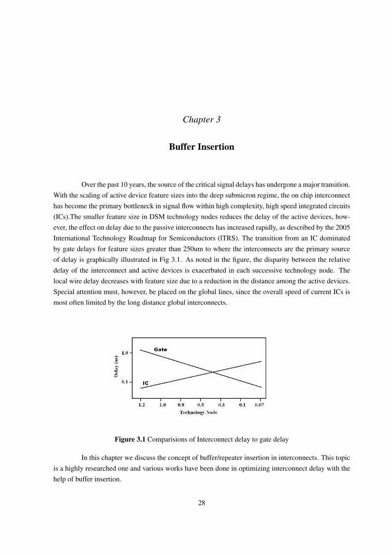
Over the past 10 years, the source of the critical signal delays has undergone a major transition.With the scaling of active device feature sizes into the deep submicron regime, the on chip interconnecthas become the primary bottleneck in signal flow within high complexity, high speed integrated circuits(ICs).The smaller feature size in DSM technology nodes reduces the delay of the active devices, how-ever, the effect on delay due to the passive interconnects has increased rapidly, as described by the 2005International Technology Roadmap for Semiconductors (lTRS). The transition from an IC dominatedby gate delays for feature sizes greater than 250um to where the interconnects are the primary sourceof delay is graphically illustrated in Fig 3.1. As noted in the figure, the disparity between the relativedelay of the interconnect and active devices is exacerbated in each successive technology node. Thelocal wire delay decreases with feature size due to a reduction in the distance among the active devices.Special attention must, however, be placed on the global lines, since the overall speed of current ICs ismost often limited by the long distance global interconnects.
Figure 3.1 Comparisions of Interconnect delay to gate delay
In this chapter we discuss the concept of buffer/repeater insertion in interconnects. This topicis a highly researched one and various works have been done in optimizing interconnect delay with thehelp of buffer insertion.
28
3.1 Background
As VLSI technology moves into the nanoscale regime, interconnect delay becomes a dominantconstraint in circuit design. A great amount of effort has been made to reduce interconnect delay andbuffer insertion appears tobe a very effective technique. It is witnessed in [13] that a large number ofbuffers are needed with current IC technology. In two recent IBM ASIC designs, 25% gates are buffers[14].
Interconnect design has become a dominant issue in high-speed integrated circuits (ICs). Withthe decreased feature size of CMOS circuits, on-chip interconnect now dominates both circuit delayand power dissipation. Many algorithms have been proposed to determine the optimum wire size thatminimizes a cost function such as the delay [49].
According to [2], the number of long interconnects doubles every three years thus increasingthe importance of on-chip interconnect further. The behavior of inductive interconnect can no longer beneglected, particularly in long, low-resistance interconnect lines [3]. As on-chip inductance becomesimportant, some wire optimization algorithms have been enhanced to consider RC impedances [4].
Uniform repeater insertion is an effective technique for driving long interconnects. Based on adistributed RC interconnect model, a repeater insertion technique to minimize signal propagation delaywas introduced in [5]. A uniform repeater structure decreases the total delay as compared to a taperedbuffer structure when driving long resistive interconnects while buffer tapering is more efficient for driv-ing large capacitive loads [6, 7]. Different techniques have been developed to enhance the model of arepeater system that considers a variety of design factors [8,14]. The drain/source capacitance of eachrepeater and multistage repeaters are considered in [15]. Noise-aware techniques for repeater insertionand wire sizing have been described in [16-19]. In [20,22], signal integrity, interconnect reliability, andmanufacturability issues have been discussed.
The work described in [23] assumes that increasing the interconnect width while maintain-ing the thickness, spacing, and height from the substrate does not reduce the signal delay since theresistance decreases and the capacitance increases. This assumption however is not accurate. Differentfactors affect the total delay such as the coupling capacitance, the driver size, and the load capacitance.Furthermore, with increasing inductive impedances, trends in the propagation delay with changing linewidth depend upon the number of repeaters and the size of the inserted repeaters.
For an RC line, repeater insertion outperforms wire sizing [24]. It is shown in this chapter thatthis behavior is not the case for an RC line. The minimum signal propagation delay always decreaseswith increasing line width for RC lines if an optimum repeater system is used. With increasing demandfor low-power ICs, different strategies have been developed to minimize power in the repeater insertion
29
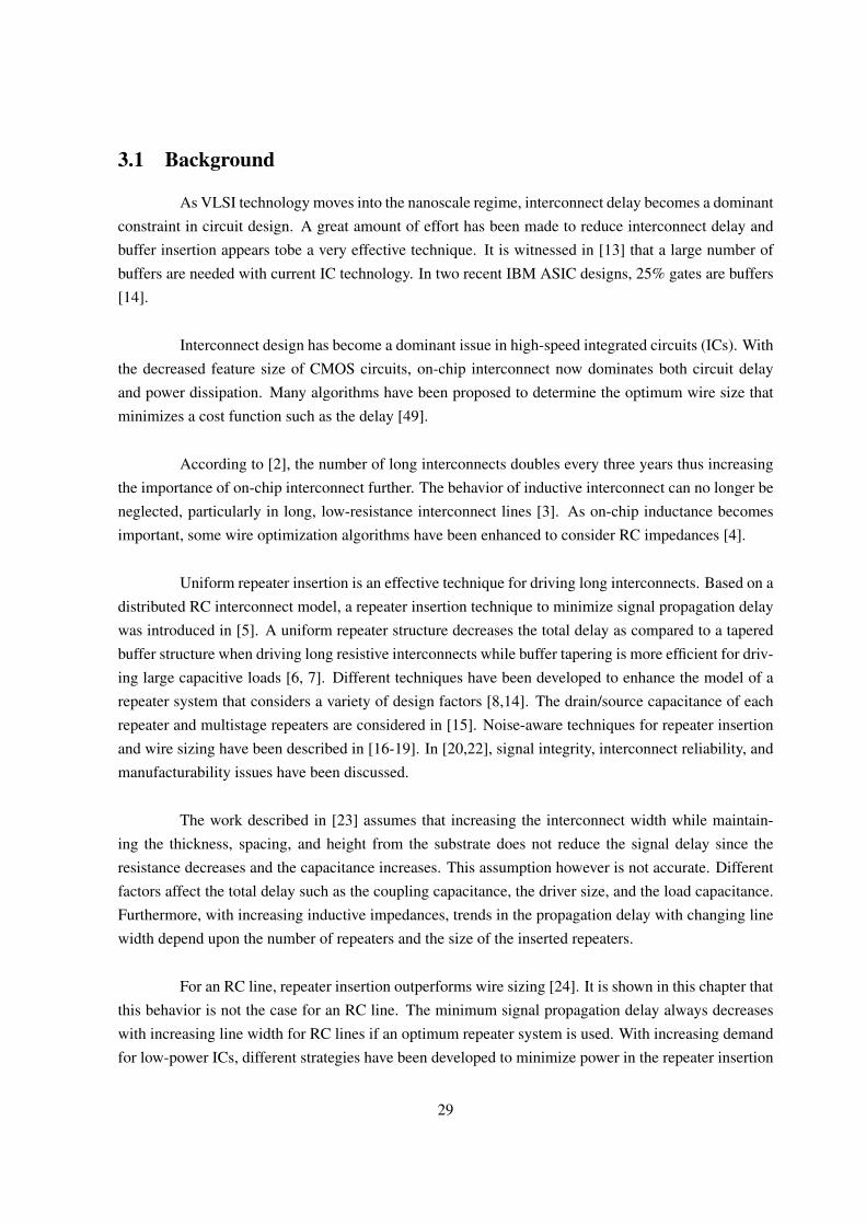
process. Power dissipation and area overhead have been considered in previous work [25-30]. The lineinductance, however, has yet to be considered in the optimization process of sizing a wire driven by arepeater system. As shown in Fig. 3.2, the minimum delay for a signal to propagate along an RC linedecreases while the power dissipation increases for wider interconnect [31].
Figure 3.2 Minimum signal propagation delay and transient power dissipation as a function of linewidth for a repeater system.
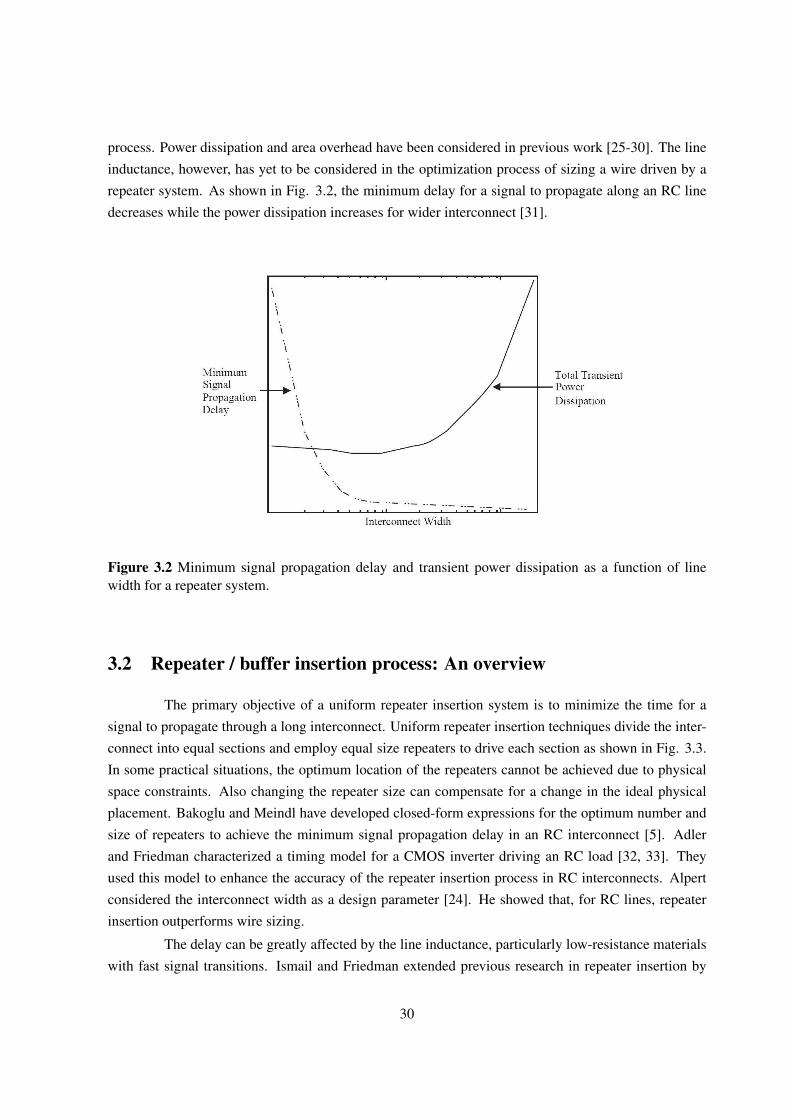
3.2 Repeater / buffer insertion process: An overview
The primary objective of a uniform repeater insertion system is to minimize the time for asignal to propagate through a long interconnect. Uniform repeater insertion techniques divide the inter-connect into equal sections and employ equal size repeaters to drive each section as shown in Fig. 3.3.In some practical situations, the optimum location of the repeaters cannot be achieved due to physicalspace constraints. Also changing the repeater size can compensate for a change in the ideal physicalplacement. Bakoglu and Meindl have developed closed-form expressions for the optimum number andsize of repeaters to achieve the minimum signal propagation delay in an RC interconnect [5]. Adlerand Friedman characterized a timing model for a CMOS inverter driving an RC load [32, 33]. Theyused this model to enhance the accuracy of the repeater insertion process in RC interconnects. Alpertconsidered the interconnect width as a design parameter [24]. He showed that, for RC lines, repeaterinsertion outperforms wire sizing.
The delay can be greatly affected by the line inductance, particularly low-resistance materialswith fast signal transitions. Ismail and Friedman extended previous research in repeater insertion by
30
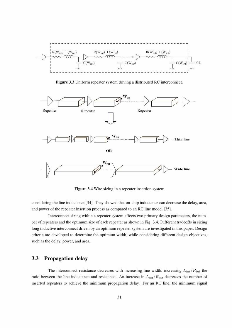
Figure 3.3 Uniform repeater system driving a distributed RC interconnect.
Figure 3.4 Wire sizing in a repeater insertion system
considering the line inductance [34]. They showed that on-chip inductance can decrease the delay, area,and power of the repeater insertion process as compared to an RC line model [35].
Interconnect sizing within a repeater system affects two primary design parameters, the num-ber of repeaters and the optimum size of each repeater as shown in Fig. 3.4. Different tradeoffs in sizinglong inductive interconnect driven by an optimum repeater system are investigated in this paper. Designcriteria are developed to determine the optimum width, while considering different design objectives,such as the delay, power, and area.
3.3 Propagation delay
The interconnect resistance decreases with increasing line width, increasing Lint/Rint theratio between the line inductance and resistance. An increase in Lint/Rint decreases the number ofinserted repeaters to achieve the minimum propagation delay. For an RC line, the minimum signal
31
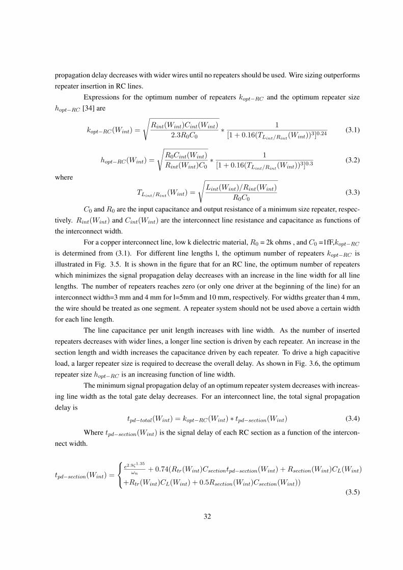
propagation delay decreases with wider wires until no repeaters should be used. Wire sizing outperformsrepeater insertion in RC lines.
Expressions for the optimum number of repeaters kopt−RC and the optimum repeater sizehopt−RC [34] are
kopt−RC(Wint) =
√Rint(Wint)Cint(Wint)
2.3R0C0∗ 1
[1 + 0.16(TLint/Rint(Wint))3]0.24
(3.1)
hopt−RC(Wint) =
√R0Cint(Wint)Rint(Wint)C0
∗ 1[1 + 0.16(TLint/Rint
(Wint))3]0.3(3.2)
where
TLint/Rint(Wint) =
√Lint(Wint)/Rint(Wint)
R0C0(3.3)
C0 and R0 are the input capacitance and output resistance of a minimum size repeater, respec-tively. Rint(Wint) and Cint(Wint) are the interconnect line resistance and capacitance as functions ofthe interconnect width.
For a copper interconnect line, low k dielectric material, R0 = 2k ohms , and C0 =1fF,kopt−RC
is determined from (3.1). For different line lengths l, the optimum number of repeaters kopt−RC isillustrated in Fig. 3.5. It is shown in the figure that for an RC line, the optimum number of repeaterswhich minimizes the signal propagation delay decreases with an increase in the line width for all linelengths. The number of repeaters reaches zero (or only one driver at the beginning of the line) for aninterconnect width=3 mm and 4 mm for l=5mm and 10 mm, respectively. For widths greater than 4 mm,the wire should be treated as one segment. A repeater system should not be used above a certain widthfor each line length.
The line capacitance per unit length increases with line width. As the number of insertedrepeaters decreases with wider lines, a longer line section is driven by each repeater. An increase in thesection length and width increases the capacitance driven by each repeater. To drive a high capacitiveload, a larger repeater size is required to decrease the overall delay. As shown in Fig. 3.6, the optimumrepeater size hopt−RC is an increasing function of line width.
The minimum signal propagation delay of an optimum repeater system decreases with increas-ing line width as the total gate delay decreases. For an interconnect line, the total signal propagationdelay is
tpd−total(Wint) = kopt−RC(Wint) ∗ tpd−section(Wint) (3.4)
Where tpd−section(Wint) is the signal delay of each RC section as a function of the intercon-nect width.
tpd−section(Wint) =
e2.9ζ1.35
ωn+ 0.74(Rtr(Wint)Csectiontpd−section(Wint) + Rsection(Wint)CL(Wint)
+Rtr(Wint)CL(Wint) + 0.5Rsection(Wint)Csection(Wint))(3.5)
32
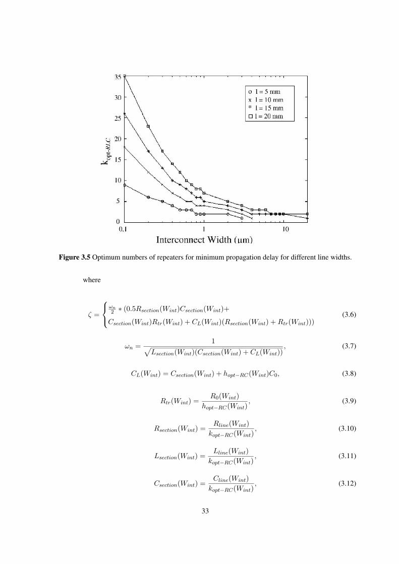
Figure 3.5 Optimum numbers of repeaters for minimum propagation delay for different line widths.
where
ζ =
ωn2 ∗ (0.5Rsection(Wint)Csection(Wint)+
Csection(Wint)Rtr(Wint) + CL(Wint)(Rsection(Wint) + Rtr(Wint)))(3.6)
ωn =1√
Lsection(Wint)(Csection(Wint) + CL(Wint)), (3.7)
CL(Wint) = Csection(Wint) + hopt−RC(Wint)C0, (3.8)
Rtr(Wint) =R0(Wint)
hopt−RC(Wint), (3.9)
Rsection(Wint) =Rline(Wint)
kopt−RC(Wint), (3.10)
Lsection(Wint) =Lline(Wint)
kopt−RC(Wint), (3.11)
Csection(Wint) =Cline(Wint)
kopt−RC(Wint), (3.12)
33
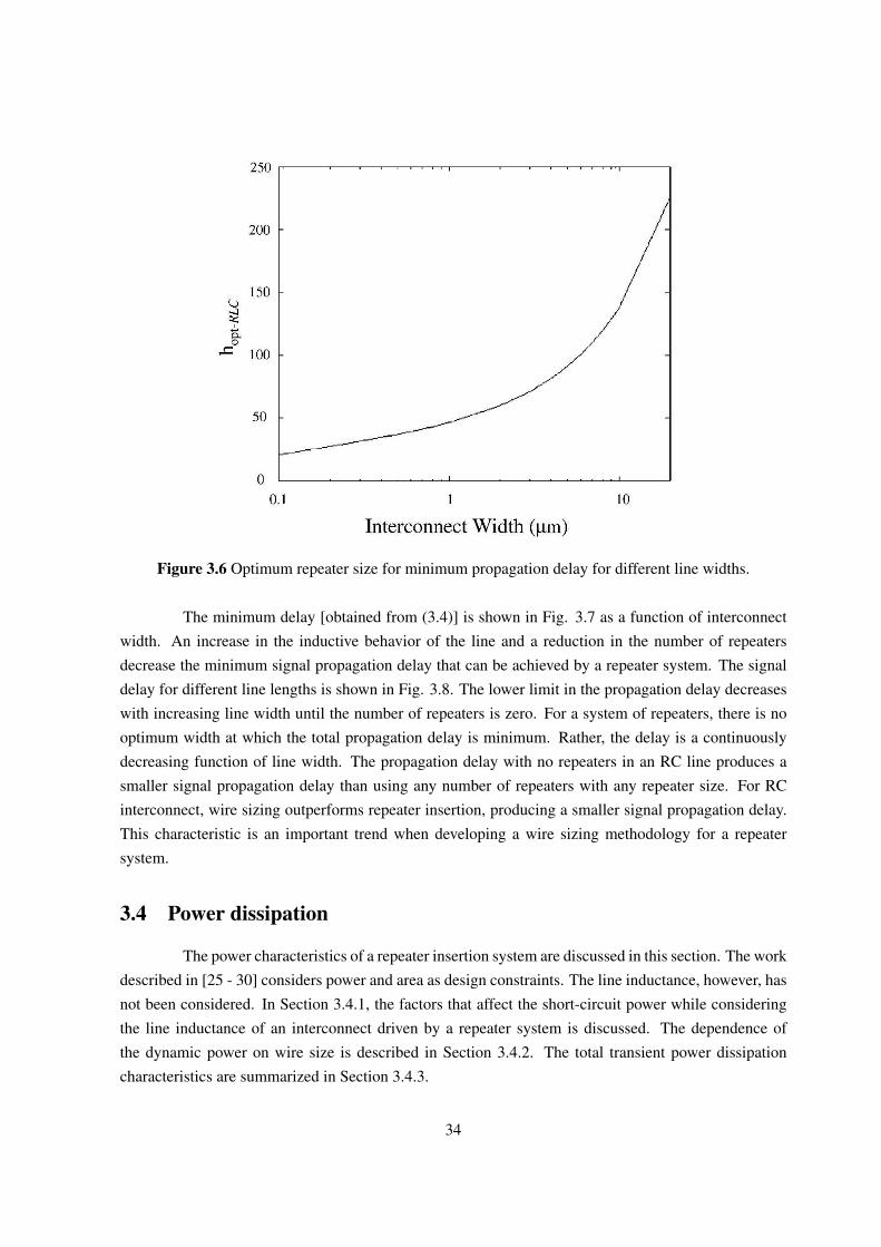
Figure 3.6 Optimum repeater size for minimum propagation delay for different line widths.
The minimum delay [obtained from (3.4)] is shown in Fig. 3.7 as a function of interconnectwidth. An increase in the inductive behavior of the line and a reduction in the number of repeatersdecrease the minimum signal propagation delay that can be achieved by a repeater system. The signaldelay for different line lengths is shown in Fig. 3.8. The lower limit in the propagation delay decreaseswith increasing line width until the number of repeaters is zero. For a system of repeaters, there is nooptimum width at which the total propagation delay is minimum. Rather, the delay is a continuouslydecreasing function of line width. The propagation delay with no repeaters in an RC line produces asmaller signal propagation delay than using any number of repeaters with any repeater size. For RCinterconnect, wire sizing outperforms repeater insertion, producing a smaller signal propagation delay.This characteristic is an important trend when developing a wire sizing methodology for a repeatersystem.
3.4 Power dissipation
The power characteristics of a repeater insertion system are discussed in this section. The workdescribed in [25 - 30] considers power and area as design constraints. The line inductance, however, hasnot been considered. In Section 3.4.1, the factors that affect the short-circuit power while consideringthe line inductance of an interconnect driven by a repeater system is discussed. The dependence ofthe dynamic power on wire size is described in Section 3.4.2. The total transient power dissipationcharacteristics are summarized in Section 3.4.3.
34
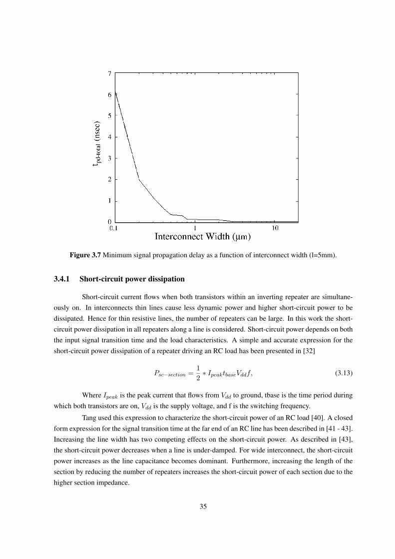
Figure 3.7 Minimum signal propagation delay as a function of interconnect width (l=5mm).
3.4.1 Short-circuit power dissipation
Short-circuit current flows when both transistors within an inverting repeater are simultane-ously on. In interconnects thin lines cause less dynamic power and higher short-circuit power to bedissipated. Hence for thin resistive lines, the number of repeaters can be large. In this work the short-circuit power dissipation in all repeaters along a line is considered. Short-circuit power depends on boththe input signal transition time and the load characteristics. A simple and accurate expression for theshort-circuit power dissipation of a repeater driving an RC load has been presented in [32]
Psc−section =12∗ IpeaktbaseVddf, (3.13)
Where Ipeak is the peak current that flows from Vdd to ground, tbase is the time period duringwhich both transistors are on, Vdd is the supply voltage, and f is the switching frequency.
Tang used this expression to characterize the short-circuit power of an RC load [40]. A closedform expression for the signal transition time at the far end of an RC line has been described in [41 - 43].Increasing the line width has two competing effects on the short-circuit power. As described in [43],the short-circuit power decreases when a line is under-damped. For wide interconnect, the short-circuitpower increases as the line capacitance becomes dominant. Furthermore, increasing the length of thesection by reducing the number of repeaters increases the short-circuit power of each section due to thehigher section impedance.
35
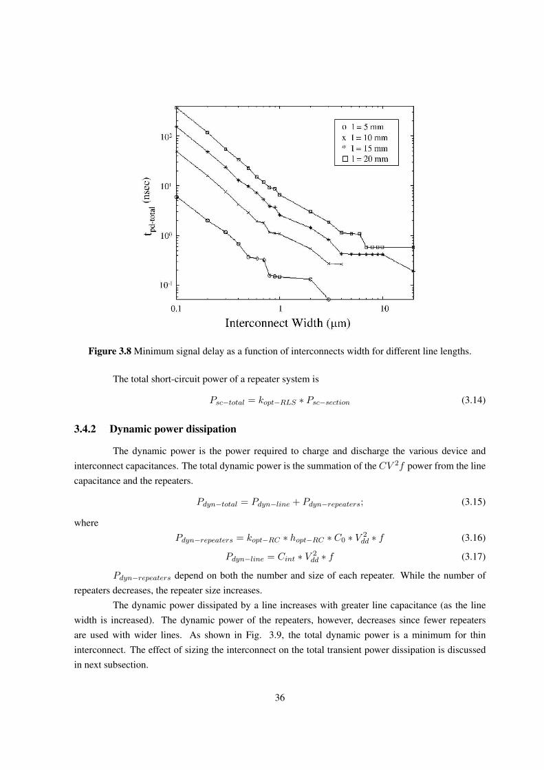
Figure 3.8 Minimum signal delay as a function of interconnects width for different line lengths.
The total short-circuit power of a repeater system is
Psc−total = kopt−RLS ∗ Psc−section (3.14)
3.4.2 Dynamic power dissipation
The dynamic power is the power required to charge and discharge the various device andinterconnect capacitances. The total dynamic power is the summation of the CV 2f power from the linecapacitance and the repeaters.
Pdyn−total = Pdyn−line + Pdyn−repeaters; (3.15)
wherePdyn−repeaters = kopt−RC ∗ hopt−RC ∗ C0 ∗ V 2
dd ∗ f (3.16)
Pdyn−line = Cint ∗ V 2dd ∗ f (3.17)
Pdyn−repeaters depend on both the number and size of each repeater. While the number ofrepeaters decreases, the repeater size increases.
The dynamic power dissipated by a line increases with greater line capacitance (as the linewidth is increased). The dynamic power of the repeaters, however, decreases since fewer repeatersare used with wider lines. As shown in Fig. 3.9, the total dynamic power is a minimum for thininterconnect. The effect of sizing the interconnect on the total transient power dissipation is discussedin next subsection.
36
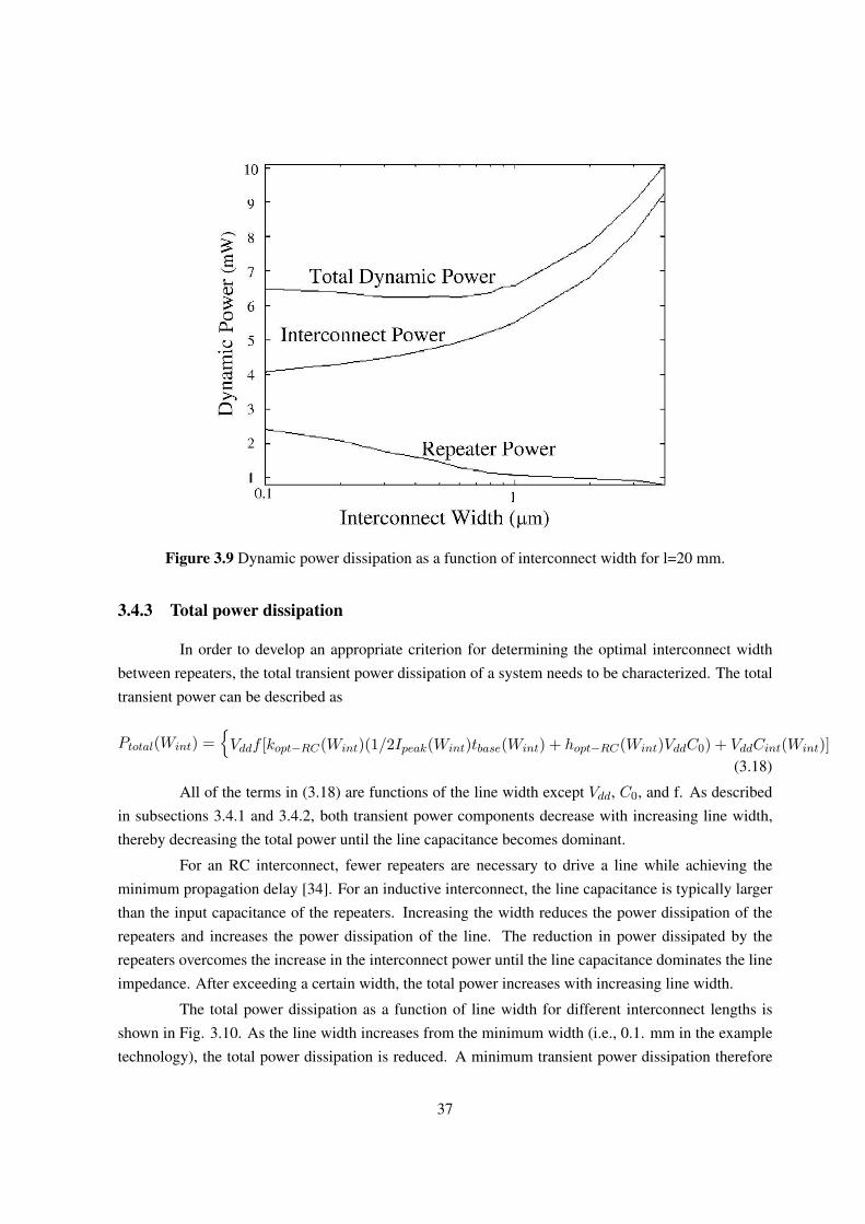
Figure 3.9 Dynamic power dissipation as a function of interconnect width for l=20 mm.
3.4.3 Total power dissipation
In order to develop an appropriate criterion for determining the optimal interconnect widthbetween repeaters, the total transient power dissipation of a system needs to be characterized. The totaltransient power can be described as
Ptotal(Wint) ={
Vddf [kopt−RC(Wint)(1/2Ipeak(Wint)tbase(Wint) + hopt−RC(Wint)VddC0) + VddCint(Wint)](3.18)
All of the terms in (3.18) are functions of the line width except Vdd, C0, and f. As describedin subsections 3.4.1 and 3.4.2, both transient power components decrease with increasing line width,thereby decreasing the total power until the line capacitance becomes dominant.
For an RC interconnect, fewer repeaters are necessary to drive a line while achieving theminimum propagation delay [34]. For an inductive interconnect, the line capacitance is typically largerthan the input capacitance of the repeaters. Increasing the width reduces the power dissipation of therepeaters and increases the power dissipation of the line. The reduction in power dissipated by therepeaters overcomes the increase in the interconnect power until the line capacitance dominates the lineimpedance. After exceeding a certain width, the total power increases with increasing line width.
The total power dissipation as a function of line width for different interconnect lengths isshown in Fig. 3.10. As the line width increases from the minimum width (i.e., 0.1. mm in the exampletechnology), the total power dissipation is reduced. A minimum transient power dissipation therefore
37
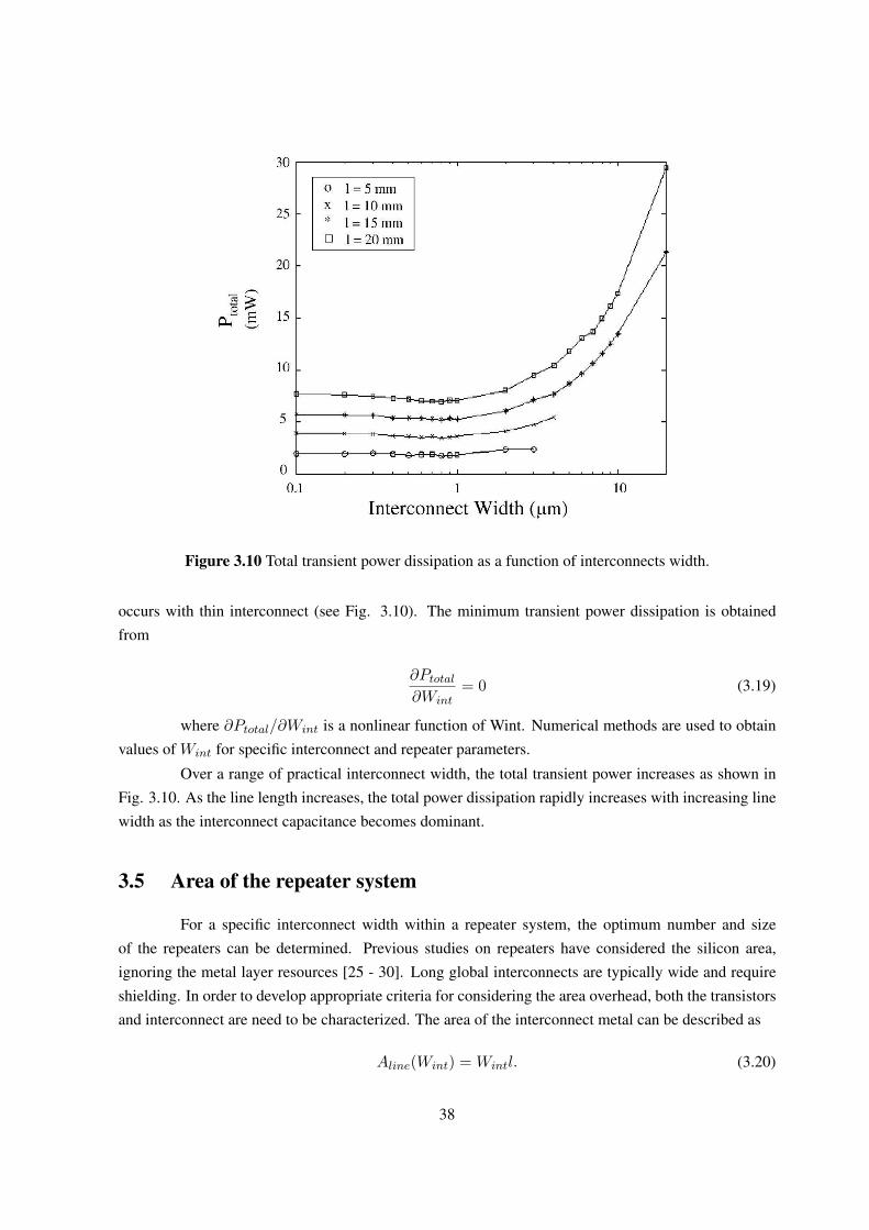
Figure 3.10 Total transient power dissipation as a function of interconnects width.
occurs with thin interconnect (see Fig. 3.10). The minimum transient power dissipation is obtainedfrom
∂Ptotal
∂Wint= 0 (3.19)
where ∂Ptotal/∂Wint is a nonlinear function of Wint. Numerical methods are used to obtainvalues of Wint for specific interconnect and repeater parameters.
Over a range of practical interconnect width, the total transient power increases as shown inFig. 3.10. As the line length increases, the total power dissipation rapidly increases with increasing linewidth as the interconnect capacitance becomes dominant.
3.5 Area of the repeater system
For a specific interconnect width within a repeater system, the optimum number and sizeof the repeaters can be determined. Previous studies on repeaters have considered the silicon area,ignoring the metal layer resources [25 - 30]. Long global interconnects are typically wide and requireshielding. In order to develop appropriate criteria for considering the area overhead, both the transistorsand interconnect are need to be characterized. The area of the interconnect metal can be described as
Aline(Wint) = Wintl. (3.20)
38
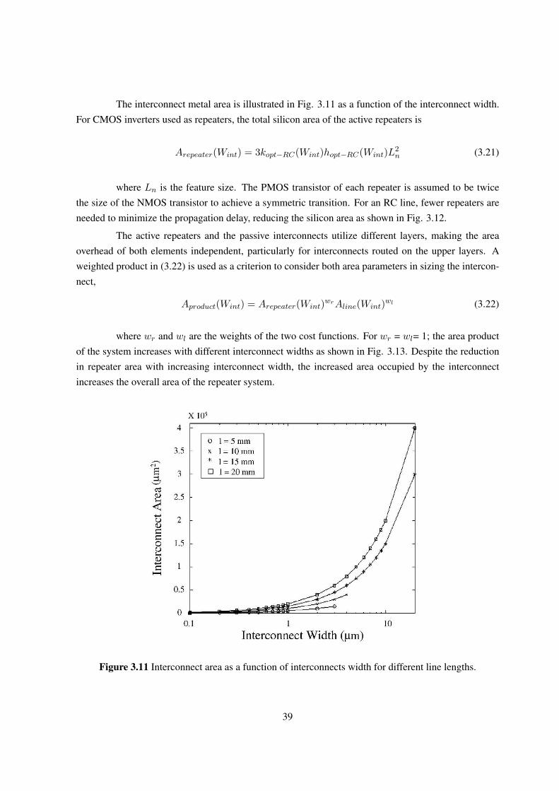
The interconnect metal area is illustrated in Fig. 3.11 as a function of the interconnect width.For CMOS inverters used as repeaters, the total silicon area of the active repeaters is
Arepeater(Wint) = 3kopt−RC(Wint)hopt−RC(Wint)L2n (3.21)
where Ln is the feature size. The PMOS transistor of each repeater is assumed to be twicethe size of the NMOS transistor to achieve a symmetric transition. For an RC line, fewer repeaters areneeded to minimize the propagation delay, reducing the silicon area as shown in Fig. 3.12.
The active repeaters and the passive interconnects utilize different layers, making the areaoverhead of both elements independent, particularly for interconnects routed on the upper layers. Aweighted product in (3.22) is used as a criterion to consider both area parameters in sizing the intercon-nect,
Aproduct(Wint) = Arepeater(Wint)wrAline(Wint)wl (3.22)
where wr and wl are the weights of the two cost functions. For wr = wl= 1; the area productof the system increases with different interconnect widths as shown in Fig. 3.13. Despite the reductionin repeater area with increasing interconnect width, the increased area occupied by the interconnectincreases the overall area of the repeater system.
Figure 3.11 Interconnect area as a function of interconnects width for different line lengths.
39
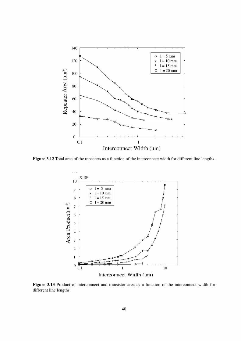
Figure 3.12 Total area of the repeaters as a function of the interconnect width for different line lengths.
Figure 3.13 Product of interconnect and transistor area as a function of the interconnect width fordifferent line lengths.
40

3.6 Design criteria for interconnect within a repeater system
In this section, different designs criteria to size interconnect within a repeater system are de-veloped. The optimization criteria can be applied to different repeater systems. In subsection 3.6.1, aconstrained system is considered. Application to an unconstrained system is discussed in subsection3.6.2.
3.6.1 Constrained systems
For a constrained system, there is a delay target (minimum speed or maximum delay) and/or alimit on the power dissipation. The minimum signal propagation delay determines a lower limit on theline width while the maximum power dissipation determines the upper limit.
If the minimum limit on the line width obtained from (3.4) is greater than the maximum widthobtained from (3.18), both limits cannot be simultaneously satisfied and one of the design constrainsneeds to be relaxed. If the minimum limit is lower than the maximum limit, both constraints can besatisfied.
For a constrained system, the transistor or metal area has an upper limit. The two factorschange differently with the width; therefore, there is a tradeoff between the two area components.
3.6.2 Unconstrained systems
For an RC line, there are four criteria to size interconnect in an unconstrained system. Thefirst criterion is for minimum power while sacrificing speed. The optimum solution for this criterion isobtained from (3.19).
The second criterion is for minimum delay. As no optimum interconnect width exists forminimum propagation delay, the practical limit is either the maximum repeater size or no repeaters, andwhichever produces a tighter constraint. The constraint in this case is either the maximum repeater sizeor the maximum line width. The optimum number of repeaters for a target line width is determinedfrom [34]. If not possible, no repeaters should be used and the design problem reduces to choosing thewidth of a single section of interconnect [31].
The third and fourth criteria are presented in the following subsections. In Section 3.6.2.1, thePower-Delay-Product (PDP) as a criterion to size an interconnect within a repeater system is described.The Power-Delay-Area-Product (PDAP) is introduced in Section 3.6.2.2 as an alternative design crite-rion.
3.6.2.1 Power-delay-product design criterion
The PDP criterion satisfies both the power dissipation and speed with no constraints on thearea. From the discussions in Sections 3.2 and 3.3, the minimum signal propagation delay of an RCinterconnect driven by a repeater system decreases with increasing line width. Alternatively, the total
41

transient power has a global minimum at a narrow width. Over the entire range of line width, thetotal transient power increases with increasing line width. At a line width smaller than the line widthfor minimum power, the power and delay both increase. An upper limit on the line width is reachedwhere the minimum propagation delay of a repeater system is attained. Beyond that limit, a singlesegment sizing criterion should be used to optimize the width according to a cost function (i.e., delay[1] or power [4143]). Between these two limits, a tradeoff exists between the power dissipation andsignal propagation delay. A single expression for the Power-Delay-Product (PDP) as a function of theinterconnect width is
PDP (Wint) = Ptotal(Wint)wp ∗ tpd−total(Wint)wd , (3.23)
where wp and wd are the weights of the cost functions. A local minimum for the PDP exists for each linelength. The minimum power delay product is obtained by numerically solving the nonlinear equation,
∂PDP
∂Wint= 0 (3.24)
The weights wp and wd describe which design objective is more highly valued.
3.6.2.2 Power-delay-area-product design criterion
The criterion described in Section 3.6.2.1 does not include the area of the system as a designparameter. In order to include the area of the system, the PDAP criterion is introduced. This criterionsatisfies both the power dissipation and speed while considering area. The Power-Delay-Area-Product(PDAP) can be used as a criterion to size the interconnect. A single expression for the PDAP as afunction of the interconnect width is
PDP (Wint) = Ptotal(Wint)wp ∗ tpd−total(Wint)wd ∗Arepeater(Wint)wr ∗Aline(Wint)wl (3.25)
A local minimum for the PDAP exists for each line length. The minimum PDAP is obtained by numer-ically solving the nonlinear equation,
∂PDP
∂Wint= 0 (3.26)
3.7 Application of interconnect design methodology
The four criteria are applied to a 65nm CMOS technology to determine the optimum solutionfor different line lengths. No limit on the maximum buffer size is assumed. In order to characterizethe line inductance in terms of the geometric dimensions, an interconnect line shielded by two groundlines is assumed. An interconnect line with resistance per square R¤ = 250mW/¤, capacitance perunit length for minimum width CWmin=66 fF/mm, and inductance per unit length for minimum widthLWmin=1nH/mm is used. For a repeater system with the following characteristics, C0 = 1fF and wp =wd 1; the optimum solution for each criterion is listed in Table 3.1. A clock signal with a 20 ps transition
42
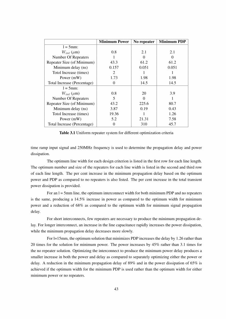
Minimum Power No repeater Minimum PDPl = 5mm:Wint (µm) 0.8 2.1 2.1
Number Of Repeaters 1 0 0Repeater Size (of Minimum) 43.3 61.2 61.2
Minimum delay (ns) 0.157 0.051 0.051Totol Increase (times) 2 1 1
Power (mW) 1.73 1.98 1.98Total Increase (Percentage) 0 14.5 14.5
l = 5mm:Wint (µm) 0.8 20 3.9
Number Of Repeaters 5 0 1Repeater Size (of Minimum) 43.2 225.6 80.7
Minimum delay (ns) 3.87 0.19 0.43Totol Increase (times) 19.36 1 1.26
Power (mW) 5.2 21.31 7.58Total Increase (Percentage) 0 310 45.7
Table 3.1 Uniform repeater system for different optimization criteria
time ramp input signal and 250MHz frequency is used to determine the propagation delay and powerdissipation.
The optimum line width for each design criterion is listed in the first row for each line length.The optimum number and size of the repeaters for each line width is listed in the second and third rowof each line length. The per cent increase in the minimum propagation delay based on the optimumpower and PDP as compared to no repeaters is also listed. The per cent increase in the total transientpower dissipation is provided.
For an l = 5mm line, the optimum interconnect width for both minimum PDP and no repeatersis the same, producing a 14.5% increase in power as compared to the optimum width for minimumpower and a reduction of 68% as compared to the optimum width for minimum signal propagationdelay.
For short interconnects, few repeaters are necessary to produce the minimum propagation de-lay. For longer interconnect, an increase in the line capacitance rapidly increases the power dissipation,while the minimum propagation delay decreases more slowly.
For l=15mm, the optimum solution that minimizes PDP increases the delay by 1.26 rather than20 times for the solution for minimum power. The power increases by 45% rather than 3.1 times forthe no repeater solution. Optimizing the interconnect to produce the minimum power delay produces asmaller increase in both the power and delay as compared to separately optimizing either the power ordelay. A reduction in the minimum propagation delay of 89% and in the power dissipation of 65% isachieved if the optimum width for the minimum PDP is used rather than the optimum width for eitherminimum power or no repeaters.
43

3.8 Need for a better approach
In this chapter various aspects of buffer insertion technique for interconnect modeling in-cluding delay reduction; power consumption and area consumed by repeaters in system are discussed.Figure 3.7 depicts the increase in propagation delay with decreasing technology size. Figure 3.5 showsthe exponential increase in the optimum number of buffer required for different interconnect length withdecreasing technology size. Hence even an optimum number of buffers are not enough to reduce theenormous increase in the propagation delay.
It is observed from graph in figure 3.9 that with decreasing interconnect width total dynamicpower and interconnect power is decreasing but the power consumed by repeaters is increasing. Thisproves to be a major factor in power optimization.
One of the major limitations of buffer insertion is the increasing number of repeaters in system.As it is shown in chapter 1, figure 1.2 shows the increasing percentage of total buffered nets in everytechnology node. Similarly figure 1.3 shows the increase in buffered cell with each next technology.Hence buffers are occupying a major portion of total area in the system. Similar results are shown infigure 3.12, which shows the exponential increase in area consumed by buffers for different interconnectlength.
All these factors are not in favor of buffer insertion for interconnect modeling. Thus a majorbreakthrough is needed to handle interconnects. Hence keeping in mind of all the problems beingfaced and to be coming with buffer insertion, in this thesis, an alternate to buffer is proposed and triedanalyzing the results. In the new approach buffer is replaced by Schmitt trigger and analyzed all theabove mentioned factors in next chapter.
44
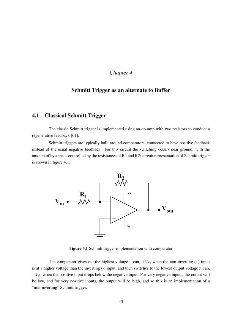
Chapter 4
Schmitt Trigger as an alternate to Buffer
4.1 Classical Schmitt Trigger
The classic Schmitt trigger is implemented using an op-amp with two resistors to conduct aregenerative feedback [61].
Schmitt triggers are typically built around comparators, connected to have positive feedbackinstead of the usual negative feedback. For this circuit the switching occurs near ground, with theamount of hysteresis controlled by the resistances of R1 and R2: circuit representation of Schmitt triggeris shown in figure 4.1.
Figure 4.1 Schmitt trigger implementation with comparator
The comparator gives out the highest voltage it can, +VS , when the non-inverting (+) inputis at a higher voltage than the inverting (-) input, and then switches to the lowest output voltage it can,−VS , when the positive input drops below the negative input. For very negative inputs, the output willbe low, and for very positive inputs, the output will be high, and so this is an implementation of a”non-inverting” Schmitt trigger.
45

For instance, if the Schmitt trigger is currently in the high state, the output will be at thepositive power supply rail (+VS). V+ is then a voltage divider between Vin and +VS . The comparatorwill switch when V+ = 0 (ground). Current conservation shows that this requires:
Vin
R1= − Vs
R2(4.1)
and so Vin must drop below - R1R2∗ Vs to get the output to switch. Once the comparator output
has switched to -VS , the threshold becomes + R1R2∗ Vs to switch back to high. So this circuit creates a
switching band centered around zero, with trigger levels ± R1R2∗ Vs. The input voltage must rise above
the top of the band, and then below the bottom of the band, for the output to switch on and then backoff. If R1 is zero or R2 is infinity (i.e., an open circuit), the band collapses to zero width, and it behavesas a standard comparator. The output characteristic is shown in the picture on the right. The value ofthe threshold T is given by R1
R2∗ Vs and the maximum value of the output M is the power supply rail.
4.2 Hysteresis in Schmitt Trigger
A phenomenon wherein two (or more) physical quantities bear a relationship which dependson prior history. More specifically, the response Y takes on different values for an increasing input Xthan for a decreasing X.
If one cycles X over an appropriate range, the plot of Y versus X gives a closed curve which isreferred to as the hysteresis loop. The response Y appears to be lagging the input X. Hysteresis occurs inmany fields of science. Schmitt trigger also have this property. Reason for hysteresis in Schmitt triggeris dual threshold voltage. Once the input voltage crosses one of the threshold voltages, output remainsabove that voltage untill it crosses the other threshold voltage. This delay results in the hysteresis curveof Schmitt trigger. figure 4.2 shows the hysteresis in classical schmitt trigger.
4.3 CMOS Schmitt Trigger
The CMOS Schmitt trigger, along with its transfer characteristics is shown in figure 4.3.
In bipolar technology, p-n-p transistors are much slower than their n-p-n counterparts [61],and the bipolar prototype for the whole circuit of Fig. 4.3 (a) is not known. A bipolar Schmitt triggerincludes an n-p-n differential pair loaded with a resistor. The circuit of Fig. 4.3(a) includes two similarsubcircuits (M1, M2, M3 and M4, M5, M6). Each of them is a highly nonlinear load for the other.However, as shown subsequently, at each transition point one subcircuit can be considered as a linearresistive load for the other. In the circuit of Fig. 4.3 (a), the bottom circuit MI, M2, M3 (which iscalled here the N-subcircuit), is loaded by the top circuit, M4, M5, M6 (P-subcircuit). As a result ofthe circuit symmetry, the inverse statement is also valid. To obtain the voltage-current characteristicsof these nonlinear loads, one can take, for example, the N-subcircuit, apply a voltage source VO, and
46
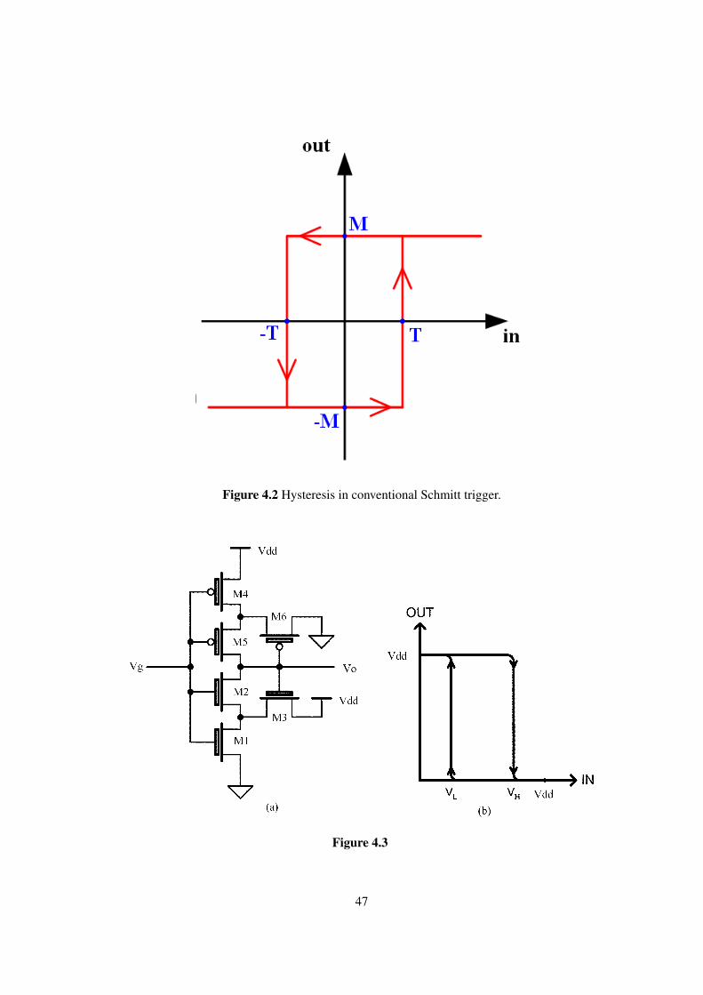
Figure 4.2 Hysteresis in conventional Schmitt trigger.
Figure 4.3
47
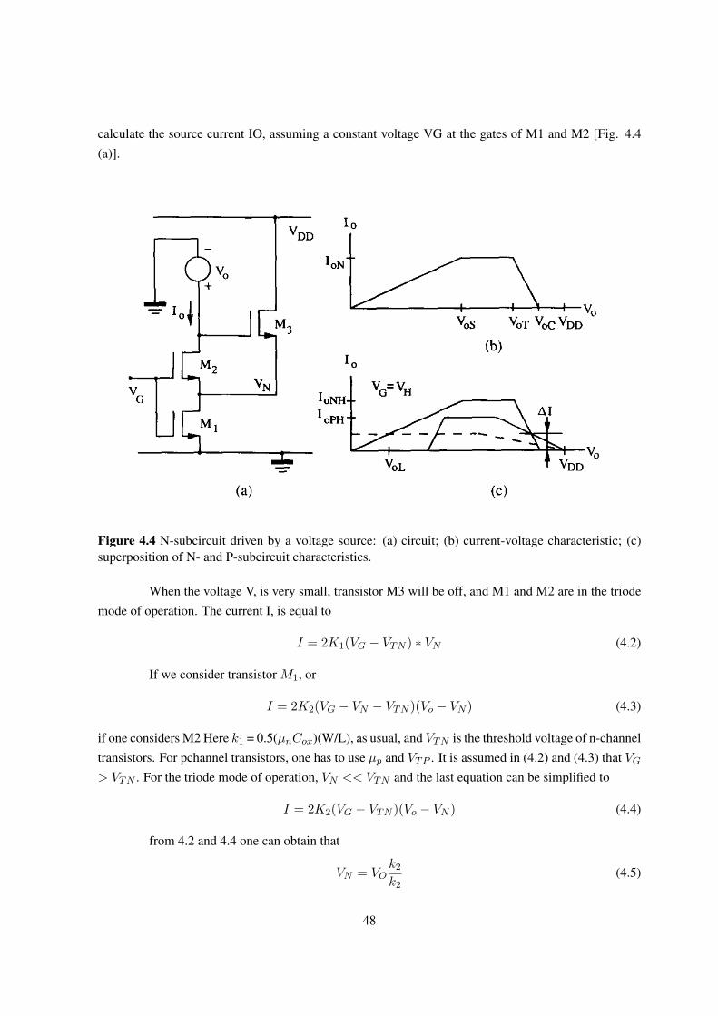
calculate the source current IO, assuming a constant voltage VG at the gates of M1 and M2 [Fig. 4.4(a)].
Figure 4.4 N-subcircuit driven by a voltage source: (a) circuit; (b) current-voltage characteristic; (c)superposition of N- and P-subcircuit characteristics.
When the voltage V, is very small, transistor M3 will be off, and M1 and M2 are in the triodemode of operation. The current I, is equal to
I = 2K1(VG − VTN ) ∗ VN (4.2)
If we consider transistor M1, or
I = 2K2(VG − VN − VTN )(Vo − VN ) (4.3)
if one considers M2 Here k1 = 0.5(µnCox)(W/L), as usual, and VTN is the threshold voltage of n-channeltransistors. For pchannel transistors, one has to use µp and VTP . It is assumed in (4.2) and (4.3) that VG
> VTN . For the triode mode of operation, VN << VTN and the last equation can be simplified to
I = 2K2(VG − VTN )(Vo − VN ) (4.4)
from 4.2 and 4.4 one can obtain that
VN = VOk2
k2(4.5)
48

andI =
2K1K2(VG − VTN )k2
Vo (4.6)
from (4.6) one can find that
RLN = [∂I
∂Vo]−1 =
k−11 + k−1
2
2(VG − VTN )(4.7)
It is seen from (4.5) and (4.7) that, in this part of the subcircuit operation, transistors M1 andM2 may be considered as a series connection of two resistors.
When Vo, increases, M2 enters into saturation (pinch-off). Then I,is determined, dependingon the considered transistor, or by
I = 2k1[VG − VTN − (VN/2)]VN (4.8)
orI = k2(VG − VN − VTN )2 (4.9)
from 4.8 and 4.9 one can find that
VN = (VG − VTN )(1−√
k1
k1 + k2) (4.10)
and does not depend on Vo. This means [Fig. 4.4(b)] that when the voltage V, achieves the value of
VoS = VG − VTN (4.11)
then current Ibecomes constant, equal to
IN =k1k2
k2(VG − VTN )2 (4.12)
Yet, an additional increase of Vo will gradually introduce some changes. When Vo achieves the value of
VoT = VG − (VG − VTN )√
k1
k1 + k2(4.13)
then transistor M3 will be turned on, V . starts to increase again, and the current I, is diminishing. WhenV, becomes equal to
VoC = VG + (VG − VTN )√
k1/k3 (4.14)
transistor M2 will be completely turned off and I, becomes equal to zero. At this instant, voltage VN
will be equal to VG - VTN and M1 is entering into saturation. Transistor M1 cames the current
IN = k1(VG − VTN )2 (4.15)
which is completely intercepted by M3. Additional increase of Vp up to VDD does not bring any changesand completes the current-voltage characteristic of the N-subcircuit.
49
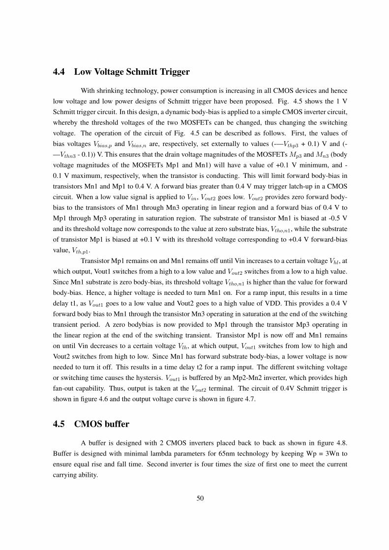
4.4 Low Voltage Schmitt Trigger
With shrinking technology, power consumption is increasing in all CMOS devices and hencelow voltage and low power designs of Schmitt trigger have been proposed. Fig. 4.5 shows the 1 VSchmitt trigger circuit. In this design, a dynamic body-bias is applied to a simple CMOS inverter circuit,whereby the threshold voltages of the two MOSFETs can be changed, thus changing the switchingvoltage. The operation of the circuit of Fig. 4.5 can be described as follows. First, the values ofbias voltages Vbias,p and Vbias,n are, respectively, set externally to values (-—Vthp3 + 0.1) V and (-—Vthn3 - 0.1)) V. This ensures that the drain voltage magnitudes of the MOSFETs Mp3 and Mn3 (bodyvoltage magnitudes of the MOSFETs Mp1 and Mn1) will have a value of +0.1 V minimum, and -0.1 V maximum, respectively, when the transistor is conducting. This will limit forward body-bias intransistors Mn1 and Mp1 to 0.4 V. A forward bias greater than 0.4 V may trigger latch-up in a CMOScircuit. When a low value signal is applied to Vin, Vout2 goes low. Vout2 provides zero forward body-bias to the transistors of Mn1 through Mn3 operating in linear region and a forward bias of 0.4 V toMp1 through Mp3 operating in saturation region. The substrate of transistor Mn1 is biased at -0.5 Vand its threshold voltage now corresponds to the value at zero substrate bias, Vtho,n1, while the substrateof transistor Mp1 is biased at +0.1 V with its threshold voltage corresponding to +0.4 V forward-biasvalue, Vth,p1.
Transistor Mp1 remains on and Mn1 remains off until Vin increases to a certain voltage Vhl, atwhich output, Vout1 switches from a high to a low value and Vout2 switches from a low to a high value.Since Mn1 substrate is zero body-bias, its threshold voltage Vtho,n1 is higher than the value for forwardbody-bias. Hence, a higher voltage is needed to turn Mn1 on. For a ramp input, this results in a timedelay t1, as Vout1 goes to a low value and Vout2 goes to a high value of VDD. This provides a 0.4 Vforward body bias to Mn1 through the transistor Mn3 operating in saturation at the end of the switchingtransient period. A zero bodybias is now provided to Mp1 through the transistor Mp3 operating inthe linear region at the end of the switching transient. Transistor Mp1 is now off and Mn1 remainson until Vin decreases to a certain voltage Vlh, at which output, Vout1 switches from low to high andVout2 switches from high to low. Since Mn1 has forward substrate body-bias, a lower voltage is nowneeded to turn it off. This results in a time delay t2 for a ramp input. The different switching voltageor switching time causes the hystersis. Vout1 is buffered by an Mp2-Mn2 inverter, which provides highfan-out capability. Thus, output is taken at the Vout2 terminal. The circuit of 0.4V Schmitt trigger isshown in figure 4.6 and the output voltage curve is shown in figure 4.7.
4.5 CMOS buffer
A buffer is designed with 2 CMOS inverters placed back to back as shown in figure 4.8.Buffer is designed with minimal lambda parameters for 65nm technology by keeping Wp = 3Wn toensure equal rise and fall time. Second inverter is four times the size of first one to meet the currentcarrying ability.
50
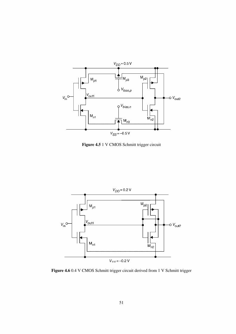
Figure 4.5 1 V CMOS Schmitt trigger circuit
Figure 4.6 0.4 V CMOS Schmitt trigger circuit derived from 1 V Schmitt trigger
51
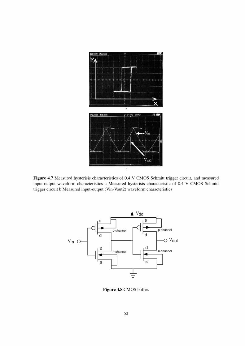
Figure 4.7 Measured hysterisis characteristics of 0.4 V CMOS Schmitt trigger circuit, and measuredinput-output waveform characteristics a Measured hysterisis characteristic of 0.4 V CMOS Schmitttrigger circuit b Measured input-output (Vin-Vout2) waveform characteristics
Figure 4.8 CMOS buffer.
52
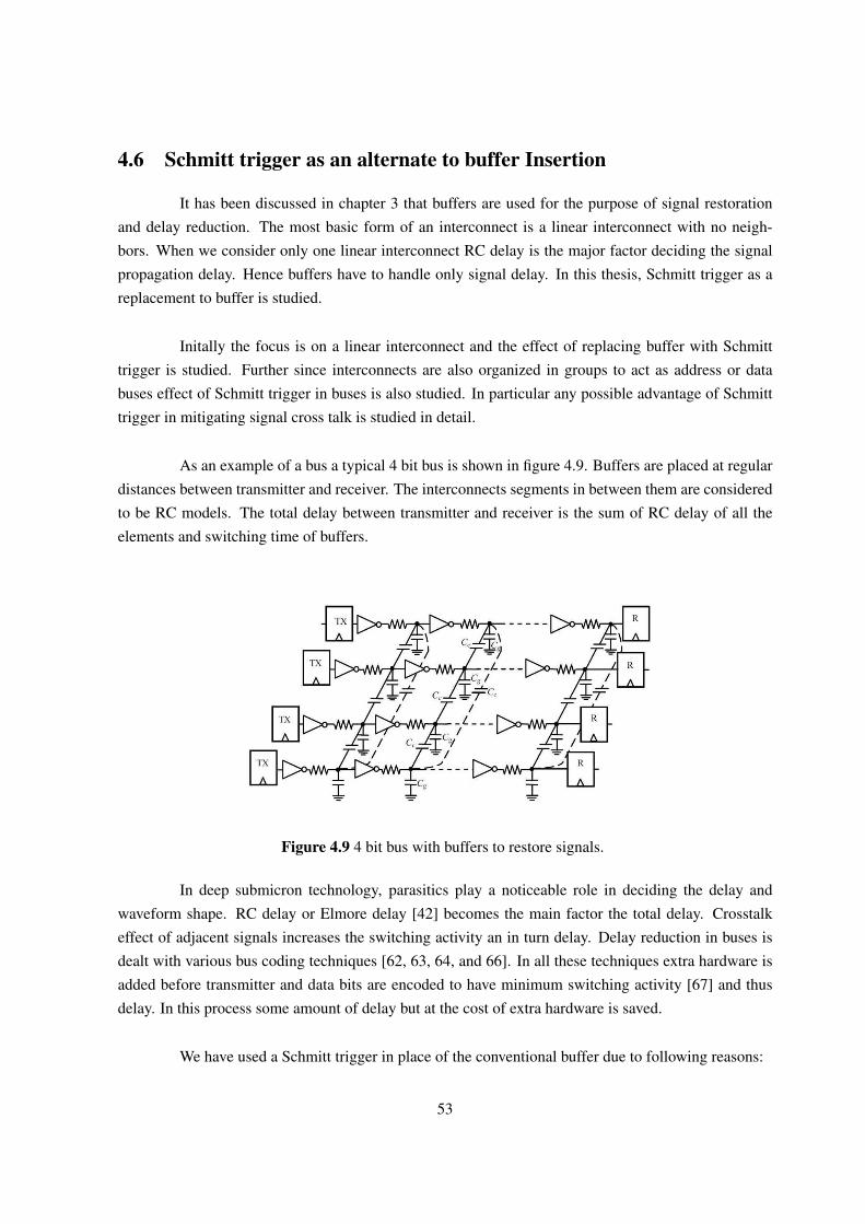
4.6 Schmitt trigger as an alternate to buffer Insertion
It has been discussed in chapter 3 that buffers are used for the purpose of signal restorationand delay reduction. The most basic form of an interconnect is a linear interconnect with no neigh-bors. When we consider only one linear interconnect RC delay is the major factor deciding the signalpropagation delay. Hence buffers have to handle only signal delay. In this thesis, Schmitt trigger as areplacement to buffer is studied.
Initally the focus is on a linear interconnect and the effect of replacing buffer with Schmitttrigger is studied. Further since interconnects are also organized in groups to act as address or databuses effect of Schmitt trigger in buses is also studied. In particular any possible advantage of Schmitttrigger in mitigating signal cross talk is studied in detail.
As an example of a bus a typical 4 bit bus is shown in figure 4.9. Buffers are placed at regulardistances between transmitter and receiver. The interconnects segments in between them are consideredto be RC models. The total delay between transmitter and receiver is the sum of RC delay of all theelements and switching time of buffers.
Figure 4.9 4 bit bus with buffers to restore signals.
In deep submicron technology, parasitics play a noticeable role in deciding the delay andwaveform shape. RC delay or Elmore delay [42] becomes the main factor the total delay. Crosstalkeffect of adjacent signals increases the switching activity an in turn delay. Delay reduction in buses isdealt with various bus coding techniques [62, 63, 64, and 66]. In all these techniques extra hardware isadded before transmitter and data bits are encoded to have minimum switching activity [67] and thusdelay. In this process some amount of delay but at the cost of extra hardware is saved.
We have used a Schmitt trigger in place of the conventional buffer due to following reasons:
53

• Schmitt trigger can act as a signal restoring circuit; this is the main reason why we have lookedinto the approach of using Schmitt trigger as an alternate of buffer in interconnects as a datarestoring element.
• Switching time of both the buffer as well as Schmitt trigger is same for a certain DSM technology,but lower threshold of the Schmitt trigger allows the reduction in rise time and hence saves interms of total delay. Although the savings in rise time delay are of few ps only, but when weconsider slowly rising signals this saving is very significant.
• With the introduction of Schmitt trigger, all sorts of bus coding techniques can be neglected andthus resulting in reduction of extra hardware and power consumption by those transistors.
• A low threshold buffer cannot be used just to lower the triggering voltage level, as it will resultin non uniform duty cycle, which is never desired in data transmission. While a low thresholdSchmitt trigger doesn’t hamper the duty cycle of the waveform due to presence of dual threshold.
• Higher noise margin of Schmitt trigger allows the circuit to handle the larger noise glitches. Thusmaking the proposed approach more efficient. With this noise margin all the 6 types of crosstalknoises are removed quite effectively.
• Reduced noise glitches result in lesser power consumption and hence help in reducing the totalpower consumed.
• Schmitt trigger has 15% more cell area, when fabricated. But major reduction in power and delayand better noise handling justifies the extra area consumed.
4.7 Conclusions
In this chapter a new circuit element called Schmitt trigger which has the property of hysteresisand dual threshold to switch between two logic levels have been studied. The element is studied as analternative to Buffers in conventional approaches. It has been observed that Schmitt trigger outplaysbuffer on the following points:
• Programmable dual threshold property of Schmitt trigger allows the designer to have lower thresh-olds for fast signal switching.
• Lower thresholds are beneficial at the time of switching too, as it would not allow all the transistorsto be in active or saturation mode.
• Noise immunity of Schmitt trigger is more than buffer due to larger bandgap.
In next chapter the simulation results with this replacement approach and then the resultsachieved would be discussed.
54
Chapter 5
Results and Discussion
5.1 NTRS 1997 predictions.
Interconnect design has become a dominant issue in high-speed integrated circuits (ICs). Withthe decreased feature size of CMOS circuits, on-chip interconnect now dominates both circuit delay andpower dissipation. The number of long interconnects doubles every three years [68], further increasingthe importance of on-chip interconnect.
The 1997 National Technology Roadmap for Semiconductors (NTRS ’97) [69] proposes ag-gressive goals for chip performance as CMOS devices approach 40 nm minimum feature sizes. Table5.1 indicates some pertinent factors which have been adapted from [69] to reflect technology shrinkageof 0.7 per generation and a corresponding doubling of clock frequency every two generations. Althoughthe clock frequency for the 250 nm technology generation in Table 5.1 is smaller than the NTRS ’97value of 750 MHz, it rises nearly to the 3000 MHz value predicted for across-chip clock frequency forhigh-performance processor chips in the 40 nm generation. CV/I data for nMOSFETs from [70] showsthat device scaling will be able to provide comparable decreases in gate delay of 0.7 per generation.
MOSFETs can meet these higher clock frequencies requirements but chip performance willbe limited by long, lossy lines to use Davidson’s terminology [71]. Since the RC time constants ofinterconnects remain the same when comparably scaled, interconnects increasingly dominate delay andcycle time as devices are scaled.
To raise clock frequencies the effects of long, lossy wires must be reduced. Only two ap-proaches are possible - reduce length or reduce loss. Interconnect length can be reduced by confininghigh-speed clocking to a limited area or by using repeaters to chop long wires into a series of shortwires. Interconnect loss can be reduced by changing materials to improve resistivity or interconnectcross sections. If the dimensions of interconnect cross sections are doubled, the interconnect’s resis-tance per unit length will drop by a factor of four while the interconnect’s capacitance per unit length(Cint) will remain the same.
55
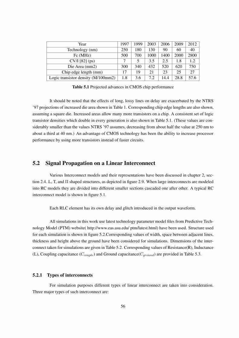
Year 1997 1999 2003 2006 2009 2012Technology (nm) 250 180 130 90 60 40
Fc (MHz) 500 700 1000 1400 2000 2800CV/I [82] (ps) 7 5 3.5 2.5 1.8 1.2
Die Area (mm2) 300 340 432 520 620 750Chip edge length (mm) 17 19 21 23 25 27
Logic transistor density (M/100mm2) 1.8 3.6 7.2 14.4 28.8 57.6
Table 5.1 Projected advances in CMOS chip performance
It should be noted that the effects of long, lossy lines on delay are exacerbated by the NTRS’97 projections of increased die area shown in Table 1. Corresponding chip edge lengths are also shown,assuming a square die. Increased areas allow many more transistors on a chip. A consistent set of logictransistor densities which double in every generation is also shown in Table 5.1. (These values are con-siderably smaller than the values NTRS ’97 assumes, decreasing from about half the value at 250 nm toabout a third at 40 nm.) An advantage of CMOS technology has been the ability to increase processorperformance by using more transistors instead of faster circuits.
5.2 Signal Propagation on a Linear Interconnect
Various Interconnect models and their representations have been discussed in chapter 2, sec-tion 2.4. L, T, and Π shaped structures, as depicted in figure 2.9. When large interconnects are modeledinto RC models they are divided into different smaller sections cascaded one after other. A typical RCinterconnect model is shown in figure 5.1.
Each RLC element has its own delay and glitch introduced in the output waveform.
All simulations in this work use latest technology parameter model files from Predictive Tech-nology Model (PTM) website( http://www.eas.asu.edu/ ptm/latest.html) have been used. Structure usedfor each simulation is shown in figure 5.2.Corresponding values of width, space between adjacent lines,thickness and height above the ground have been considered for simulations. Dimensions of the inter-connect taken for simulations are given in Table 5.2. Corresponding values of Resistance(R), Inductance(L), Coupling capacitance (Ccouple) and Ground capacitance(Cground) are provided in Table 5.3.
5.2.1 Types of interconnects
For simulation purposes different types of linear interconnect are taken into consideration.Three major types of such interconnect are:
56
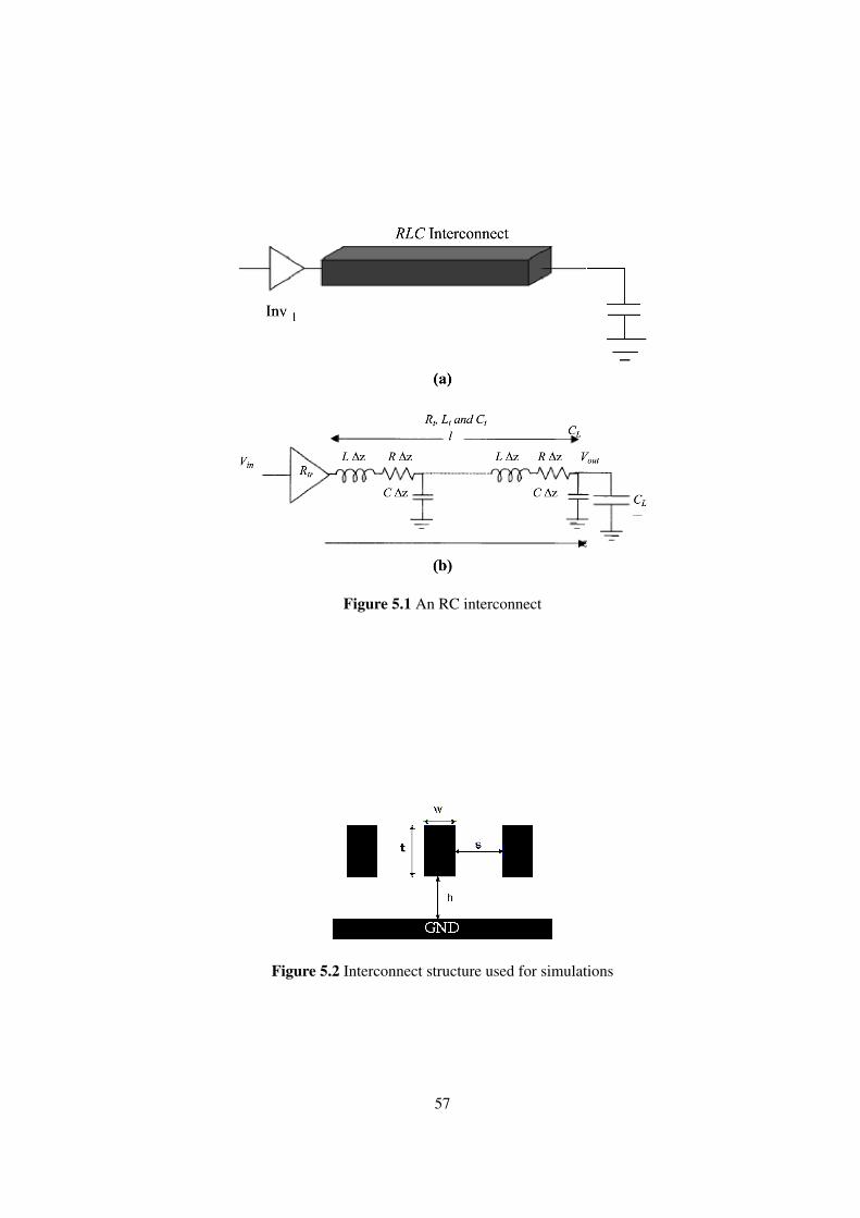
Figure 5.1 An RC interconnect
Figure 5.2 Interconnect structure used for simulations
57
Tech L t h K W S(mm) (um) (um) (um) (um)
2 0.45 0.65 3.5 0.28 0.28180 5 0.65 0.65 3.5 0.35 0.35nm 10 1.25 0.65 3.5 0.80 0.80
2 0.45 0.45 3.2 0.20 0.20130 5 0.45 0.45 3.2 0.28 0.28nm 10 1.20 0.45 3.2 0.60 0.60
2 0.30 0.30 2.8 0.15 0.1590 5 0.45 0.30 2.8 0.20 0.20nm 10 1.20 0.30 2.8 0.50 0.50
2 0.20 0.20 2.2 0.10 0.1065 5 0.35 0.2 2.2 0.14 0.14nm 10 1.2 0.2 2.2 0.45 0.45
Table 5.2 Interconnect dimensions
• Local interconnect
• Intermediate Interconnect
• Global Interconnect
Local interconnects are the smallest length interconnects typically used to connect the consec-utive logic blocks. While designing these interconnects the width is kept to be half of the height andthickness of the interconnect. Minimum spacing between two local interconnects is kept to be at leastequal to the width of line. Interconnects up to 2mm length are considered in this category. Intermediateinterconnects are the larger interconnects typically used to connect long distance placed logic blocks.These can have a length of around 5mm. While designing these interconnects the typical ratio in width,thickness and height is kept to be 4:9:6. Global interconnects are the longest interconnects possible onthe chip. These are mainly used to provide power supplies to different parts of the chip. Typical lengthof these interconnects can be as long as 10mm also. The ratio of width, thickness and height is kept tobe 4:8:3.
In the first test case different RC elements of length 2mm,5mm and 10mm for 180nm tech-nology are taken into consideration. A fast rising signal with operating frequency of 500MHz is fed atinput end. Output is observed at output end for each length and shown in figure 5.3.
In figure 5.3 waveform 1 is the input signal with operating voltage of 1.8V and frequency500MHz. interconnects are considered to be only RC elements in this simulation. Waveform 2 is theoutput wave appearing at the end of 2mm long RC interconnect. It can be observed that the output isdelayed and parabolic shaped due to Elmore delays. It is observed that though the output is maintaining
58
Tech L R L Ccouple Cground
(mm) (ohms) (nH) (fF) (fF)2 349 3.6 94.8 33.2
180 5 483 9.72 246 104nm 10 880 16.5 435 214
2 488 3.6 122 34130 5 1242 10.5 312.5 82.5nm 10 2444 21.2 612.5 173.4
2 977 3.8 107.2 38.290 5 2444 10.6 268 97nm 10 4888 22.4 536.3 194.2
2 2200 3.99 107.2 38.265 5 5500 10.9 268 97nm 10 11000 23.2 536.2 194.2
Table 5.3 Interconnect Resistance, Inductance and Capacitance values
the same frequency as of input signal its gets delayed in reaching the output.
When waveform 3 is observed, which corresponds to a 5mm long, interconnect at same tech-nology node with same input signal, it is found that due to larger R and C factors the signal is moredelayed and deformed. To reach 50 percent of Vdd it has taken almost 40% of the clock cycle and sameimplies in reaching to 10% of Vdd while switching back to zero level. Thus there is an alarming issuedue to such a high RC delay factors. The situation is worse in 10mm length. When waveform 4 isobserved, which corresponds to 10 mm long interconnect, it can be seen that the output is not delayedby such a large time amount that it’s not even reaching the 50% of Vdd during the complete clock cy-cle. Same pattern is observed while switching from high to low. This situation makes the use of largeinterconnects almost impossible for data transmission, frequency mismatch can result in a large amountof data loss.
When RLC models are to be considered, the situation becomes more complicated. Addedmutual inductance adds some more distortions to the output signal. Effect of inductance on the samesignal is shown in figure 5.4.
By observing the output waveforms in figure 5.4 it can be observed that interconnect induc-tance adds noise glitches to the output signal. Hence the signal is delayed and due to added noise glitchesit consumes more power.
Same trends have been observed for smaller feature sizes also. Output results for same in-terconnect length for 90nm and 65nm technologies are simulated. Figure 5.5 and 5.6 show the results
59
Figure 5.3 Output end signals on a 2mm, 5mm and 10mm RC interconnect at 180nm technology.
corresponding to 90nm and 65nm technology respectively.
Thus it is concluded that in DSM with each next generation technology linear interconnectsare facing the following problems
• RC delay in the output signal
• Noise induced due to interconnect inductance
• Extra power consumption.
In the incoming section, the conventional approach to handle these problem that is with bufferInsertion is discussed.
5.3 Effect of Buffer Insertion on Delay, Noise and Power Reduction
With the continuous trend of Very Large Scale Integration (VLSI) circuits technology scalingdown and frequency increasing, interconnect delay becomes a significant bottleneck in system perfor-mances. This trend is a result of increased resistance of the interconnect when feature sizes enter thenanometer era. From International Technology Roadmap for Semiconductors (ITRS) projection, inter-connect delay can contribute to more than 50% of the delay when the feature size is beyond 180 nm. As
60
Figure 5.4 Output end signals on a 2mm, 5mm and 10mm RLC interconnect at 180nm technology.
Figure 5.5 Output end signals on a 2mm, 5mm and 10mm RLC interconnect at 90nm technology.
61
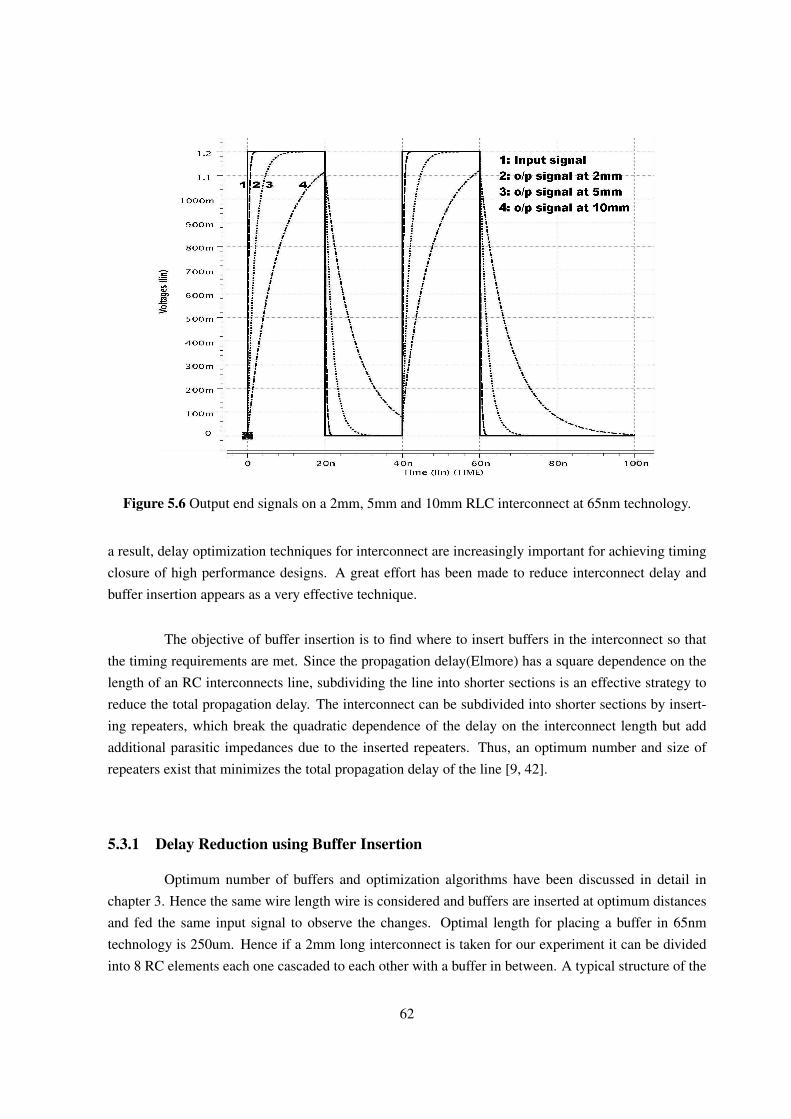
Figure 5.6 Output end signals on a 2mm, 5mm and 10mm RLC interconnect at 65nm technology.
a result, delay optimization techniques for interconnect are increasingly important for achieving timingclosure of high performance designs. A great effort has been made to reduce interconnect delay andbuffer insertion appears as a very effective technique.
The objective of buffer insertion is to find where to insert buffers in the interconnect so thatthe timing requirements are met. Since the propagation delay(Elmore) has a square dependence on thelength of an RC interconnects line, subdividing the line into shorter sections is an effective strategy toreduce the total propagation delay. The interconnect can be subdivided into shorter sections by insert-ing repeaters, which break the quadratic dependence of the delay on the interconnect length but addadditional parasitic impedances due to the inserted repeaters. Thus, an optimum number and size ofrepeaters exist that minimizes the total propagation delay of the line [9, 42].
5.3.1 Delay Reduction using Buffer Insertion
Optimum number of buffers and optimization algorithms have been discussed in detail inchapter 3. Hence the same wire length wire is considered and buffers are inserted at optimum distancesand fed the same input signal to observe the changes. Optimal length for placing a buffer in 65nmtechnology is 250um. Hence if a 2mm long interconnect is taken for our experiment it can be dividedinto 8 RC elements each one cascaded to each other with a buffer in between. A typical structure of the
62
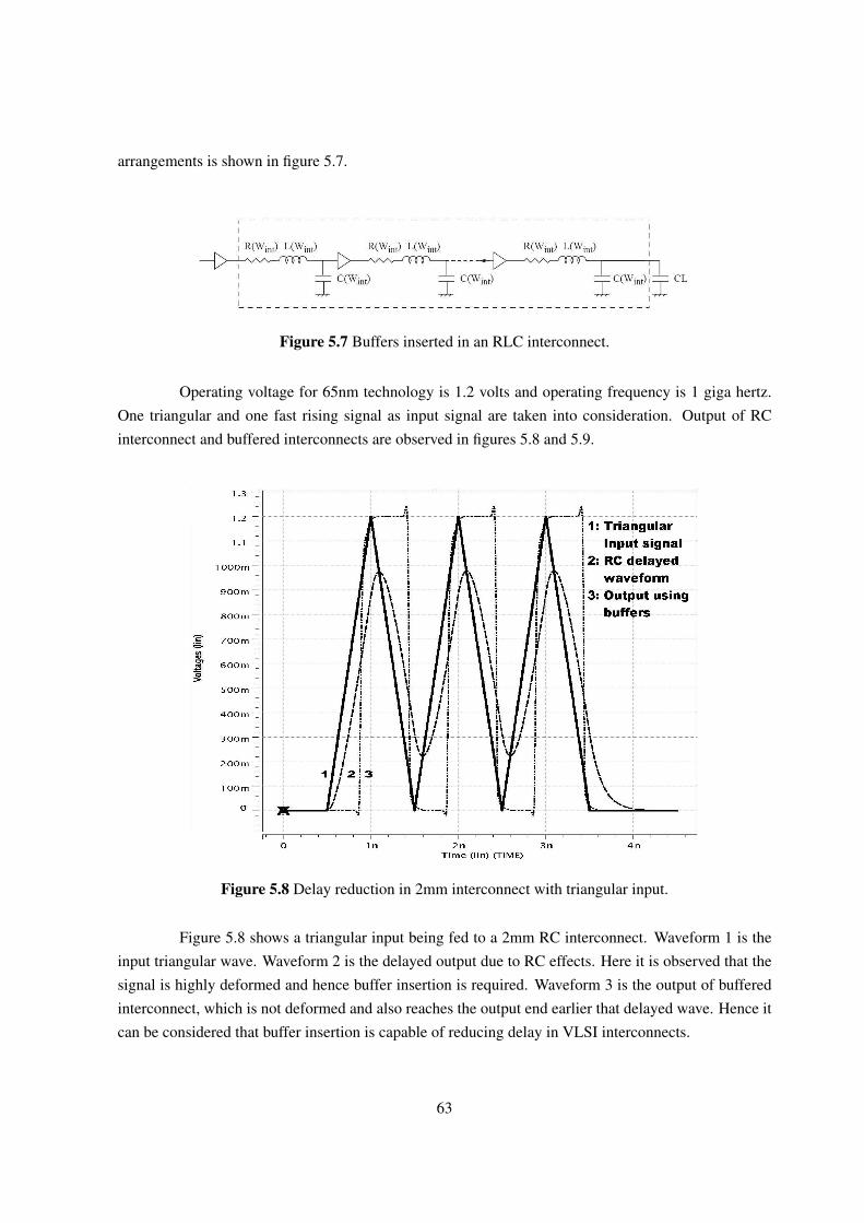
arrangements is shown in figure 5.7.
Figure 5.7 Buffers inserted in an RLC interconnect.
Operating voltage for 65nm technology is 1.2 volts and operating frequency is 1 giga hertz.One triangular and one fast rising signal as input signal are taken into consideration. Output of RCinterconnect and buffered interconnects are observed in figures 5.8 and 5.9.
Figure 5.8 Delay reduction in 2mm interconnect with triangular input.
Figure 5.8 shows a triangular input being fed to a 2mm RC interconnect. Waveform 1 is theinput triangular wave. Waveform 2 is the delayed output due to RC effects. Here it is observed that thesignal is highly deformed and hence buffer insertion is required. Waveform 3 is the output of bufferedinterconnect, which is not deformed and also reaches the output end earlier that delayed wave. Hence itcan be considered that buffer insertion is capable of reducing delay in VLSI interconnects.
63
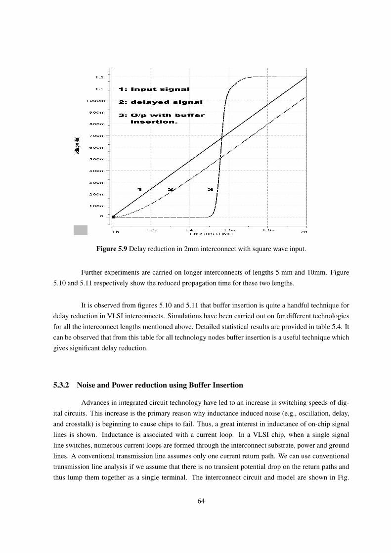
Figure 5.9 Delay reduction in 2mm interconnect with square wave input.
Further experiments are carried on longer interconnects of lengths 5 mm and 10mm. Figure5.10 and 5.11 respectively show the reduced propagation time for these two lengths.
It is observed from figures 5.10 and 5.11 that buffer insertion is quite a handful technique fordelay reduction in VLSI interconnects. Simulations have been carried out on for different technologiesfor all the interconnect lengths mentioned above. Detailed statistical results are provided in table 5.4. Itcan be observed that from this table for all technology nodes buffer insertion is a useful technique whichgives significant delay reduction.
5.3.2 Noise and Power reduction using Buffer Insertion
Advances in integrated circuit technology have led to an increase in switching speeds of dig-ital circuits. This increase is the primary reason why inductance induced noise (e.g., oscillation, delay,and crosstalk) is beginning to cause chips to fail. Thus, a great interest in inductance of on-chip signallines is shown. Inductance is associated with a current loop. In a VLSI chip, when a single signalline switches, numerous current loops are formed through the interconnect substrate, power and groundlines. A conventional transmission line assumes only one current return path. We can use conventionaltransmission line analysis if we assume that there is no transient potential drop on the return paths andthus lump them together as a single terminal. The interconnect circuit and model are shown in Fig.
64
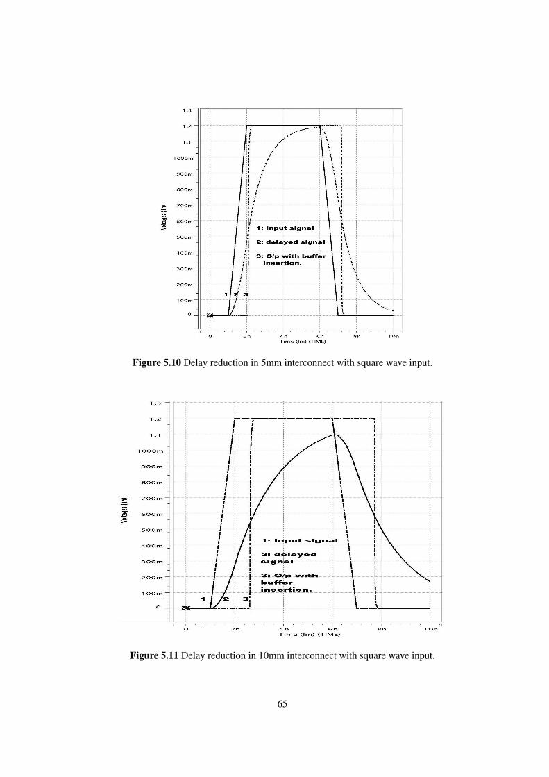
Figure 5.10 Delay reduction in 5mm interconnect with square wave input.
Figure 5.11 Delay reduction in 10mm interconnect with square wave input.
65
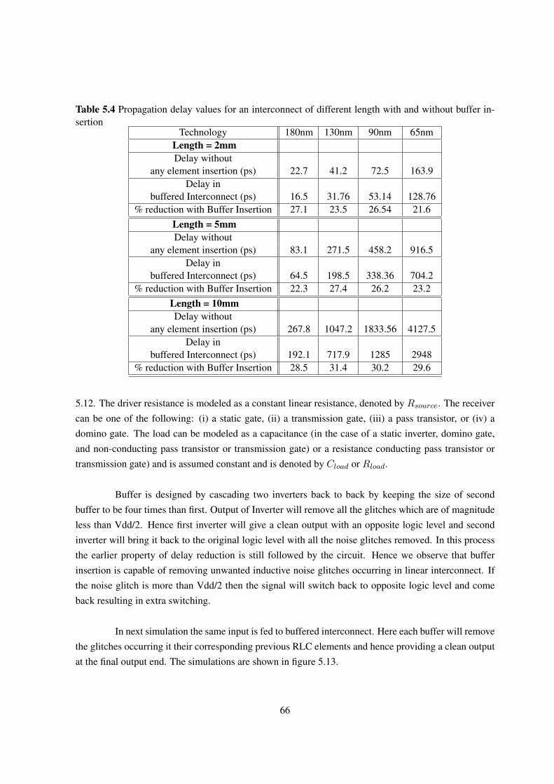
Table 5.4 Propagation delay values for an interconnect of different length with and without buffer in-sertion
Technology 180nm 130nm 90nm 65nmLength = 2mmDelay without
any element insertion (ps) 22.7 41.2 72.5 163.9Delay in
buffered Interconnect (ps) 16.5 31.76 53.14 128.76% reduction with Buffer Insertion 27.1 23.5 26.54 21.6
Length = 5mmDelay without
any element insertion (ps) 83.1 271.5 458.2 916.5Delay in
buffered Interconnect (ps) 64.5 198.5 338.36 704.2% reduction with Buffer Insertion 22.3 27.4 26.2 23.2
Length = 10mmDelay without
any element insertion (ps) 267.8 1047.2 1833.56 4127.5Delay in
buffered Interconnect (ps) 192.1 717.9 1285 2948% reduction with Buffer Insertion 28.5 31.4 30.2 29.6
5.12. The driver resistance is modeled as a constant linear resistance, denoted by Rsource. The receivercan be one of the following: (i) a static gate, (ii) a transmission gate, (iii) a pass transistor, or (iv) adomino gate. The load can be modeled as a capacitance (in the case of a static inverter, domino gate,and non-conducting pass transistor or transmission gate) or a resistance conducting pass transistor ortransmission gate) and is assumed constant and is denoted by Cload or Rload.
Buffer is designed by cascading two inverters back to back by keeping the size of secondbuffer to be four times than first. Output of Inverter will remove all the glitches which are of magnitudeless than Vdd/2. Hence first inverter will give a clean output with an opposite logic level and secondinverter will bring it back to the original logic level with all the noise glitches removed. In this processthe earlier property of delay reduction is still followed by the circuit. Hence we observe that bufferinsertion is capable of removing unwanted inductive noise glitches occurring in linear interconnect. Ifthe noise glitch is more than Vdd/2 then the signal will switch back to opposite logic level and comeback resulting in extra switching.
In next simulation the same input is fed to buffered interconnect. Here each buffer will removethe glitches occurring it their corresponding previous RLC elements and hence providing a clean outputat the final output end. The simulations are shown in figure 5.13.
66
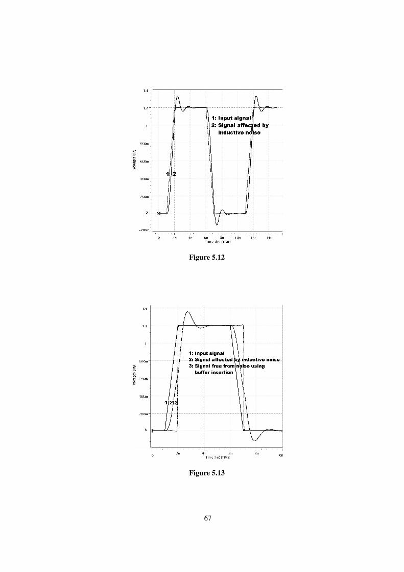
Figure 5.12
Figure 5.13
67

Reduced noise glitches result in less current in the circuit. This implies that for the samecircuit operation we would be operating with lower power consumption. Detailed analysis of reducedpower in the interconnect is shown in table 5.5.
Table 5.5 Power consumption values for an interconnect of different length with and without bufferinsertion approach.
Technology 180nm 130nm 90nm 65nmLength = 2mm
Power consumptionin the interconnect (µW) 111.2 151.5 198.5 245.2
Power consumptionin buffered Interconnect (µW) 89.6 121.6 153.6 177.6
% reduction with Buffer Insertion 19.5 19.9 22.8 27.7Length = 5mm
Power consumptionin the interconnect (µW) 301.2 410.2 504.6 614.5
Power consumptionin buffered Interconnect (µW) 231.1 340 417.5 497.28
% reduction with Buffer Insertion 23.3 18.1 17.3 19.1Length = 10mm
Power consumptionin the interconnect (µW) 620.1 921.4 1114.6 1340
Power consumptionin buffered Interconnect (µW) 531.6 715 907.6 1094.1
% reduction with buffer Insertion 14.4 22.4 19.1 18.4
While buffer insertion is a useful technique, as discussed in chapter 4, the limitations of bufferinsertion technique have forced us to think of new algorithms and approaches. In next section the effectof using Schmitt trigger in place of buffer in linear interconnects would be studied.
5.4 Effect of Schmitt trigger on delay, noise and power reduction in Lin-ear Interconnects
In chapter 4, it was suggested that replacing buffers with Schmitt trigger may have an advan-tage. In this section effect of Schmitt trigger in interconnect delay, noise and power reduction would beanalyzed and discussed.
68
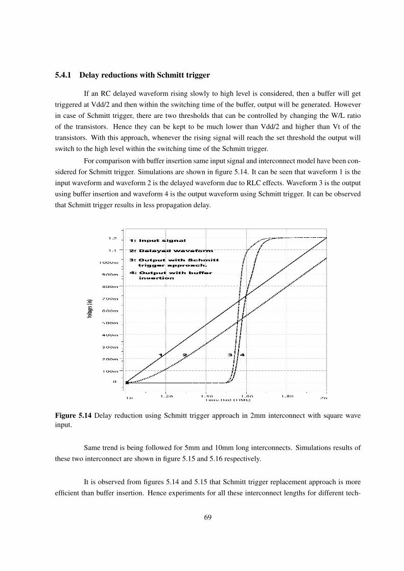
5.4.1 Delay reductions with Schmitt trigger
If an RC delayed waveform rising slowly to high level is considered, then a buffer will gettriggered at Vdd/2 and then within the switching time of the buffer, output will be generated. Howeverin case of Schmitt trigger, there are two thresholds that can be controlled by changing the W/L ratioof the transistors. Hence they can be kept to be much lower than Vdd/2 and higher than Vt of thetransistors. With this approach, whenever the rising signal will reach the set threshold the output willswitch to the high level within the switching time of the Schmitt trigger.
For comparison with buffer insertion same input signal and interconnect model have been con-sidered for Schmitt trigger. Simulations are shown in figure 5.14. It can be seen that waveform 1 is theinput waveform and waveform 2 is the delayed waveform due to RLC effects. Waveform 3 is the outputusing buffer insertion and waveform 4 is the output waveform using Schmitt trigger. It can be observedthat Schmitt trigger results in less propagation delay.
Figure 5.14 Delay reduction using Schmitt trigger approach in 2mm interconnect with square waveinput.
Same trend is being followed for 5mm and 10mm long interconnects. Simulations results ofthese two interconnect are shown in figure 5.15 and 5.16 respectively.
It is observed from figures 5.14 and 5.15 that Schmitt trigger replacement approach is moreefficient than buffer insertion. Hence experiments for all these interconnect lengths for different tech-
69
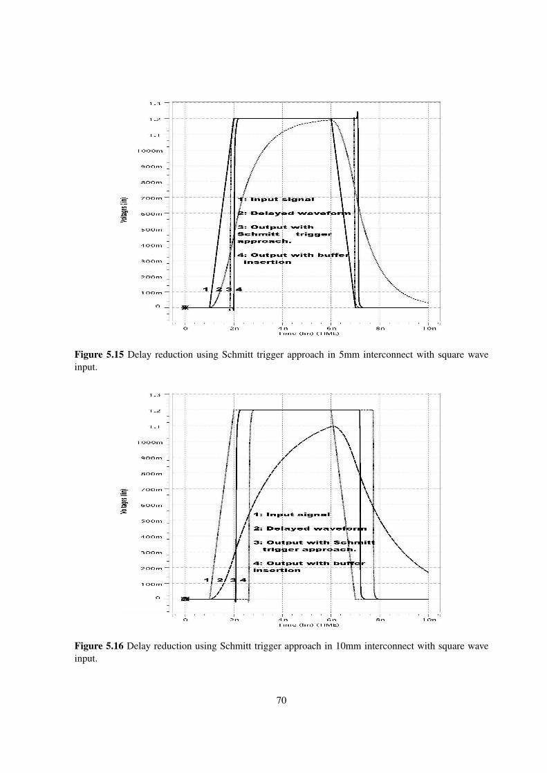
Figure 5.15 Delay reduction using Schmitt trigger approach in 5mm interconnect with square waveinput.
Figure 5.16 Delay reduction using Schmitt trigger approach in 10mm interconnect with square waveinput.
70

nology nodes have been conducted. Detailed results are provided in Table 5.6.
Table 5.6 Propagation delay values for an interconnect of different length with buffer insertion and delayreduction using Schmitt trigger approach
Technology 180nm 130nm 90nm 65nmLength = 2mm
Delay inbuffered Interconnect (ps) 16.5 31.76 53.14 128.76
Delay withSchmitt trigger approach (ps) 12.3 21.65 38.1 95.6
% reduction with Schmitt trigger 25.3 31.4 28.3 25.6Length = 5mm
Delay inbuffered Interconnect (ps) 64.5 198.5 338.36 704.2
Delay withSchmitt trigger approach (ps) 46.1 148.8 236.8 514
% reduction with Schmitt trigger 28.5 25 30 27Length = 10mm
Delay inbuffered Interconnect (ps) 192.1 717.9 1285 2948
Delay withSchmitt trigger approach (ps) 134.4 490.3 842.5 2098.2
% reduction with Schmitt trigger 29.8 31.7 34.5 28.2
5.4.2 Noise and power reduction with Schmitt trigger approach
As it has been discussed in section 5.3, interconnects do suffer from inductive noise. Bufferinsertion, along with reducing the signal propagation delay, is quite capable of handling inductive noisesand thus reducing the power consumption too (table 5.5). Buffers are quite useful until we have noiseglitches with magnitude less than Vdd/2. In these cases there won’t be any unwanted switch to theopposite logic level due to noisy signal. But when the glitches are of higher magnitude, unwantedswitching to opposite level can occur due to triggering of buffer at Vdd/2. These switches always addto extra power consumption too. Noise reduction using Schmitt trigger approach is shown in figure 5.17.
However, Schmitt trigger possesses dual threshold voltage. Hence to switch from on logiclevel to other the noisy signal has to cross both the thresholds. Thus more noise margin is obtained withSchmitt trigger. Extensive noise analysis has been carried out by introducing artificial noise at Vdd/2of the input signal. The noise is generated by coupling the signal with a high frequency waveform.Thus glitches are produced at Vdd/2. When this waveform is fed to buffered interconnect, buffer willmake unwanted switching from high to low due to instability at Vdd/2 and thus adding extra delay to
71
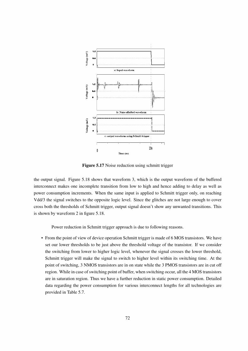
Figure 5.17 Noise reduction using schmitt trigger
the output signal. Figure 5.18 shows that waveform 3, which is the output waveform of the bufferedinterconnect makes one incomplete transition from low to high and hence adding to delay as well aspower consumption increments. When the same input is applied to Schmitt trigger only, on reachingVdd/3 the signal switches to the opposite logic level. Since the glitches are not large enough to covercross both the thresholds of Schmitt trigger, output signal doesn’t show any unwanted transitions. Thisis shown by waveform 2 in figure 5.18.
Power reduction in Schmitt trigger approach is due to following reasons.
• From the point of view of device operation Schmitt trigger is made of 6 MOS transistors. We haveset our lower thresholds to be just above the threshold voltage of the transistor. If we considerthe switching from lower to higher logic level, whenever the signal crosses the lower threshold,Schmitt trigger will make the signal to switch to higher level within its switching time. At thepoint of switching, 3 NMOS transistors are in on state while the 3 PMOS transistors are in cut offregion. While in case of switching point of buffer, when switching occur, all the 4 MOS transistorsare in saturation region. Thus we have a further reduction in static power consumption. Detaileddata regarding the power consumption for various interconnect lengths for all technologies areprovided in Table 5.7.
72
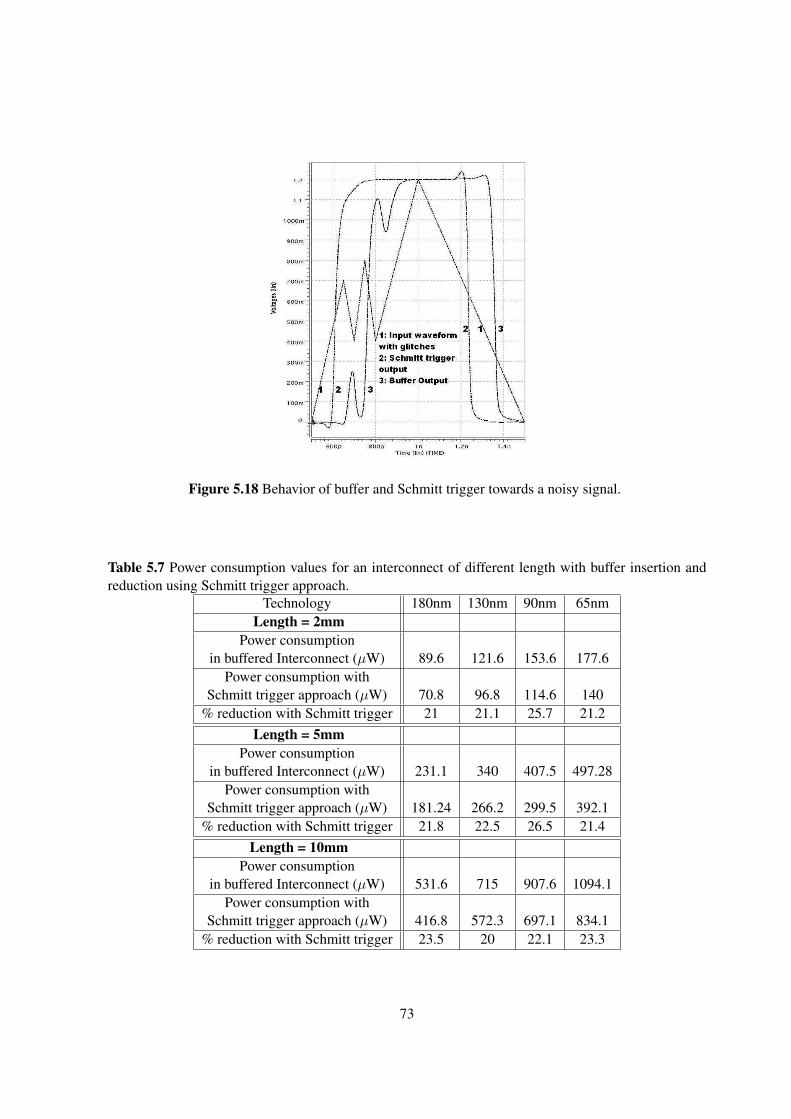
Figure 5.18 Behavior of buffer and Schmitt trigger towards a noisy signal.
Table 5.7 Power consumption values for an interconnect of different length with buffer insertion andreduction using Schmitt trigger approach.
Technology 180nm 130nm 90nm 65nmLength = 2mm
Power consumptionin buffered Interconnect (µW) 89.6 121.6 153.6 177.6
Power consumption withSchmitt trigger approach (µW) 70.8 96.8 114.6 140
% reduction with Schmitt trigger 21 21.1 25.7 21.2Length = 5mm
Power consumptionin buffered Interconnect (µW) 231.1 340 407.5 497.28
Power consumption withSchmitt trigger approach (µW) 181.24 266.2 299.5 392.1
% reduction with Schmitt trigger 21.8 22.5 26.5 21.4Length = 10mm
Power consumptionin buffered Interconnect (µW) 531.6 715 907.6 1094.1
Power consumption withSchmitt trigger approach (µW) 416.8 572.3 697.1 834.1
% reduction with Schmitt trigger 23.5 20 22.1 23.3
73
5.5 Replacement of Buffers in Buses
In deep-submicron technology, minimizing the propagation delay and power consumptionon buses is the most important design objective in system-on-chip design. In particular, the couplingeffects between wires on the bus that can cause serious problems such as crosstalk delay, noise andpower consumption. One of the fastest growing areas in computing industry is the provision of highthroughput low power digital signal processing (DSP) and communication systems. The recent trendsshow that the systems-on-chip (SOC) used for such systems are becoming increasingly more complexas they add more functionality, while having size, performance, and power consumption constraints.The basic problems affecting the issue are:
• Minimizing the crosstalk delay.
• Minimizing the power consumption on bus,
Bus coding techniques are often used to reduce delay and power in interconnect buses. It is knownthat lowering transition-switching activity on the bit lines of bus leads to a significant reduction in the(dynamic) bus power consumption.
5.5.1 Signal Propagation in Buses
In a data bus interconnects are laid side by side very close to each other. Parallel data bits aretransmitted on them simultaneously. The values on adjacent interconnects always keep changing withnew data values. Every rise or fall in the data value in one line always affects the adjacent lines due tothe existence of coupling capacitance in between them. At 180nm technology this affect was very lowbecause the interconnects were laid very far from each other. Thus the coupling capacitance value wasvery low or close to negligible. This implied that the crosstalk noise glitches were not so prominent inthe transmitted signal. Also lower values of interconnect resistance and capacitances result in lower RCdelay in 180nm technology. Thus we get the transmitted signal on buses to be only slightly delayed withnegligible noise glitches. Figure 5.19 shows the data bits transmitted on all the bits of a 2mm long 8bitbus.
However the case is not the same in case of current technologies. When we come to DSMtechnologies, feature size reduces a lot, which results in increased coupling capacitance and higher re-sistance values. These factors results in a tremendous increase in R and C values and hence a largerElmore Delay and due to very less distance between adjacent interconnects the coupling capacitancevalue is very high. Hence crosstalk noise has a much larger magnitude. Figure 5.20 shows the databeing transmitted on an 8 bit bus.
74
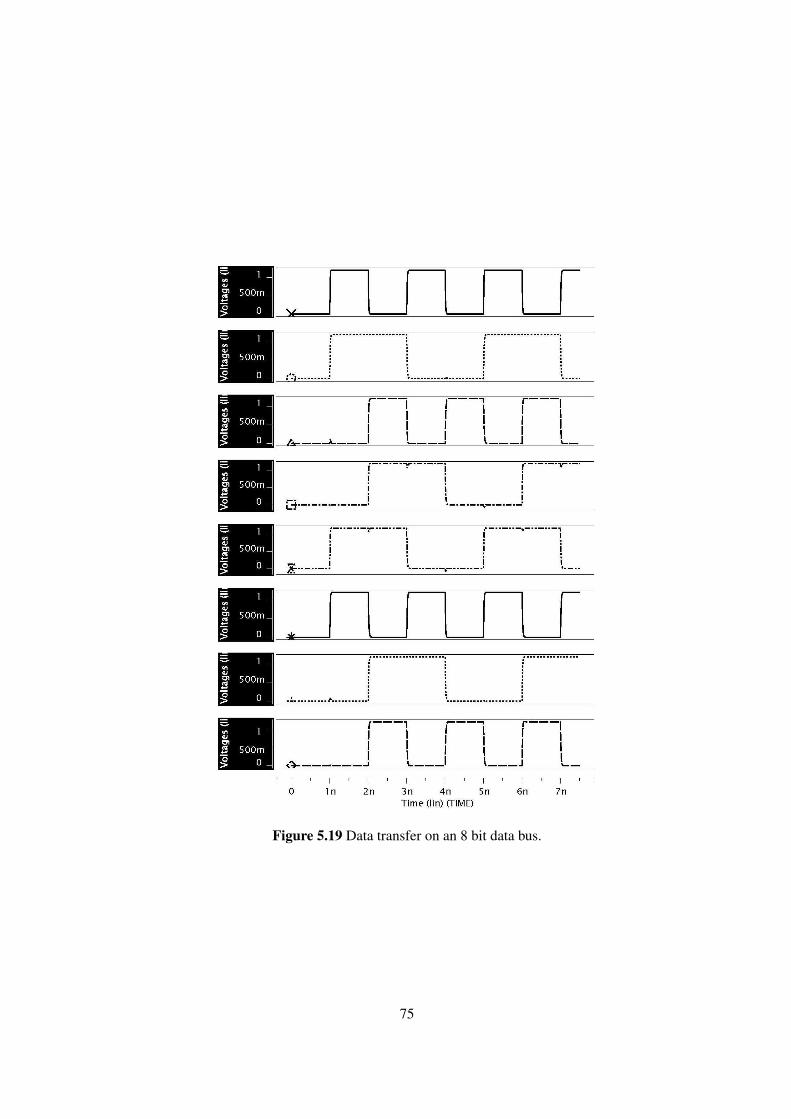
Figure 5.19 Data transfer on an 8 bit data bus.
75
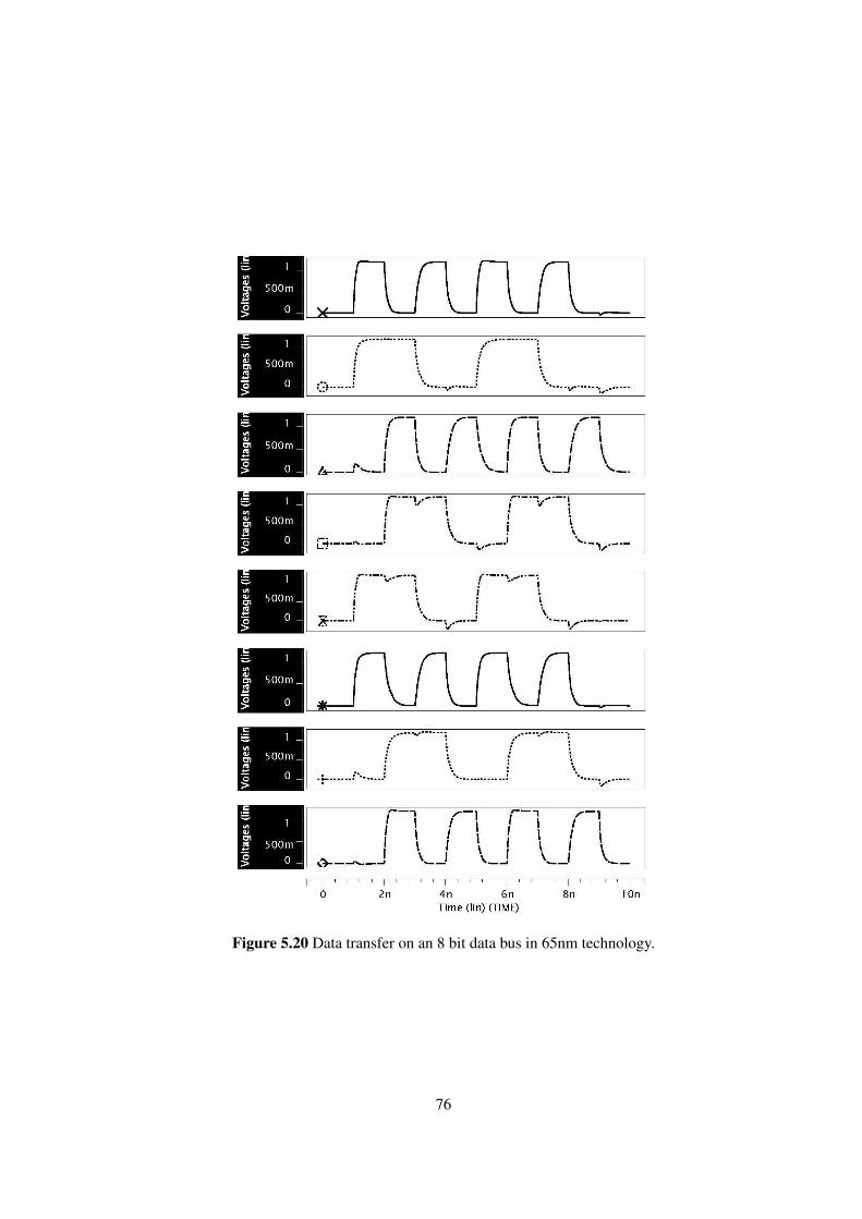
Figure 5.20 Data transfer on an 8 bit data bus in 65nm technology.
76
Thus we observe that data signal on data buses in DSM technologies get distorted due to delayas well as crosstalk noises. Various bus coding techniques have earlier been proposed to recover thesignal from these effects. These are discussed in next subsection.
5.5.2 Definitions and Related Work
5.5.2.1 Low Power Coding
The power dissipation in the bus depends on data transition activity. We refer to codes thatreduce the average transition activity as low-power codes (LPCs). A simple but effective LPC is thebus-invert code in which the data is inverted and an invert bit is sent to the decoder if the current dataword differs from the previous data word in more than half the number of bits. The effectiveness of bus-invert coding decreases with increase in the bus width .Therefore, for wide buses, the bus is partitionedinto several sub-buses each with its own invert bit. It should be noted that bus-invert coding is nonlinear.It has been shown that linear codes do not reduce transition activity.
5.5.2.2 Crosstalk Avoidance Coding
The delay of a wire in the bus depends on the transitions on the wire and wires adjacent toit. The worst-case delay of a wire is . The purpose of the crosstalk avoidance coding is to limit theworst-case delay to . Crosstalk avoidance codes (CACs) are proposed to reduce the worst-case delayby ensuring that a transition from one codeword to another codeword does not cause adjacent wiresto transition in opposite directions. We refer to this condition as Forbidden transition (FT) condition.Shielding the wires of a bus by inserting grounded wires between adjacent wires is the simplest way tosatisfy this condition. A forbidden transition code (FTC) that requires fewer wires that shielding hasbeen proposed. There is no linear code that satisfies the FT condition while requiring fewer wires thanshielding. The number of valid n-bit code words, MFT (n) satisfying the forbidden transition conditionis, MFT (n) = Fn+2; where Fn is the Fibonacci sequence satisfying Fn = Fn−1+ Fn−2 with initialconditions F1 = F2 = 1.
The worst-case delay can also be reduced to by avoiding bit patterns ”010” and ”101” fromevery codeword. We refer to this condition as Forbidden pattern (FP) condition. The simplest methodto satisfy the FP condition is to duplicate every data wire whereby each data bit is transmitted usingtwo adjacent wires. There is no linear forbidden pattern code (FPC) that satisfies the FP condition whilerequiring fewer wires than duplication. The number of codewords is given by, MFP (n) = 2 Fn+1; whereFn is the Fibonacci sequence. However, this increase in the number of codewords translates into at mostone additional data bit that can be encoded for the same n.
77
5.5.2.3 Error Control Coding
Error control is possible if the Hamming distance between any two codewords in the codebookis greater than one. If the minimum Hamming distance between any two codewords is two, then allsingle errors appearing on the bus can be detected.
If the minimum Hamming distance is three, then all single errors can be corrected. Errordetection is simpler to implement than error correction but requires retransmission of the data when anerror occurs. In systematic codes, a few redundant bits are appended to the input bits to generate thecodeword. Hamming code is an example of a linear systematic error correcting code.
5.5.2.4 CAC coding Schemes
Coding involves mapping k data/information bits to n code bits resulting in an (n, k) codehaving a code rate of k/n. This mapping can be done either by involving memory or without memory(memory less). However, codes with memory, in general, suffer from error propagation at the decoder.Complex techniques, such as those employed in communication systems, are needed to ensure that errorpropagation is not catastrophic. Such techniques are prohibitively complex to be used for on-chip busesin the foreseeable future .Further, even when error propagation is not a concern; codes with memorytend to have significantly more complex encoders and decoders as compared to memoryless codes. Somemory less codes are preferred over codes with memory. The design of memoryless codes boils downto determining a subset C of size/cardinality 2k consisting of n-bit vectors derived from the set S ofall possible 2n n-bit vectors. The code words in C, referred to as the codebook, provide delay, power,or reliability benefits by satisfying specific constraints. For example, a (n, k, p) CAC achieves delayreduction by reducing the worst-case delay of a bus from (1+4 ) 0 to (1+p ) 0, where 0 is the delay of acrosstalk-free bus line, 0 is the ratio of the coupling capacitance to the bulk capacitance, and p = 1,2 or3 is the maximum coupling. For large buses, it is impractical to encode all k bits at once due to the largecomplexity in the design and the implementation of the codec. Therefore, partial coding is employedwherein the bus is broken into sub-buses of smaller width which are encoded into sub-channels. Thisis because the hardware complexity grows exponentially with k. For example: a 32 bit bus broken intosub buses of size 3 and encoded into buses of size 4(3-4 encoding).
The mapping between data words and codewords is shown as well. This coding scheme re-moves the FT condition present in the data. Using the partial coding technique described above, an arrayof ten of these simple coders could be used to implement a crosstalk immune 32-bit bus with 53 wires.When compared to a 63-wire shielded channel, this amounts to cutting ten wires from the channel forthe cost of a handful of gates.
5.5.2.5 Relationship between delay and crosstalk
The equations for computing the delay between two data tuples dt (data already available onthe bus lines), dt+1 (data that have to be transmitted on the bus lines) at time instances ’t’ and ’t+1’ is
78
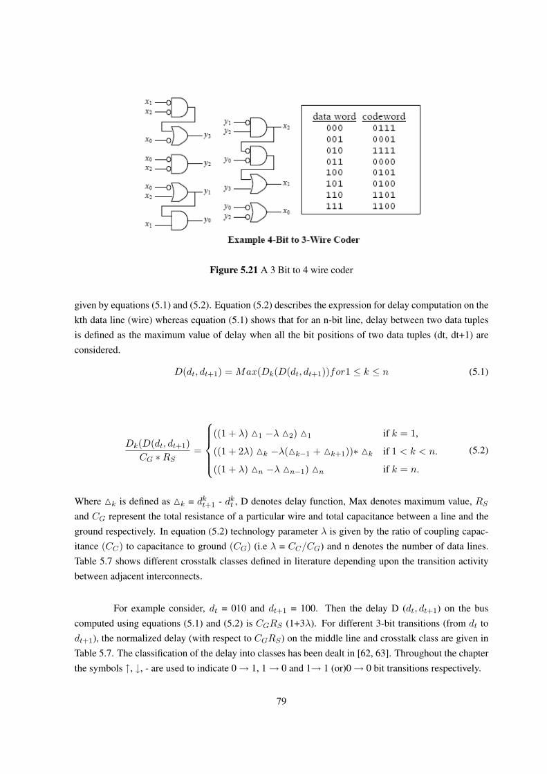
Figure 5.21 A 3 Bit to 4 wire coder
given by equations (5.1) and (5.2). Equation (5.2) describes the expression for delay computation on thekth data line (wire) whereas equation (5.1) shows that for an n-bit line, delay between two data tuplesis defined as the maximum value of delay when all the bit positions of two data tuples (dt, dt+1) areconsidered.
D(dt, dt+1) = Max(Dk(D(dt, dt+1))for1 ≤ k ≤ n (5.1)
Dk(D(dt, dt+1)CG ∗RS
=
((1 + λ) M1 −λ M2) M1 if k = 1,
((1 + 2λ) Mk −λ(Mk−1 + Mk+1))∗ Mk if 1 < k < n.
((1 + λ) Mn −λ Mn−1) Mn if k = n.
(5.2)
Where Mk is defined as Mk = dkt+1 - dk
t , D denotes delay function, Max denotes maximum value, RS
and CG represent the total resistance of a particular wire and total capacitance between a line and theground respectively. In equation (5.2) technology parameter λ is given by the ratio of coupling capac-itance (CC) to capacitance to ground (CG) (i.e λ = CC/CG) and n denotes the number of data lines.Table 5.7 shows different crosstalk classes defined in literature depending upon the transition activitybetween adjacent interconnects.
For example consider, dt = 010 and dt+1 = 100. Then the delay D (dt, dt+1) on the buscomputed using equations (5.1) and (5.2) is CGRS (1+3λ). For different 3-bit transitions (from dt todt+1), the normalized delay (with respect to CGRS) on the middle line and crosstalk class are given inTable 5.7. The classification of the delay into classes has been dealt in [62, 63]. Throughout the chapterthe symbols ↑, ↓, - are used to indicate 0 → 1, 1 → 0 and 1→ 1 (or)0 → 0 bit transitions respectively.
79
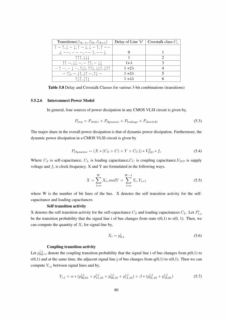
Transitions(4k−1,4k,4k+1) Delay of Line ′k′ Crosstalk class Cc
↑ − ↑, ↓ − ↓, ↑ − ↓, ↓ − ↑, ↑ −−,↓ −−,−−−,−− ↑,−− ↓ 0 1
↑↑↑, ↓↓↓ 1 2↑↑ −, ↓↓ −,− ↑↑,− ↓↓ 1+λ 3
− ↑ −,− ↓ −, ↑↓↓, ↑↑↓, ↓↓↑, ↓↑↑ 1 +2λ 4− ↑↓,− ↓↑, ↓↑ −, ↑↓ − 1 +3λ 5
↑↓↑, ↓↑↓ 1 +4λ 6
Table 5.8 Delay and Crosstalk Classes for various 3-bit combinations (transitions)
5.5.2.6 Interconnect Power Model
In general, four sources of power dissipation in any CMOS VLSI circuit is given by,
Pavg = Pstatic + Pdynamic + Pleakage + Pshortckt (5.3)
The major share in the overall power dissipation is that of dynamic power dissipation. Furthermore, thedynamic power dissipation in a CMOS VLSI circuit is given by
PDynamic = (X ∗ (CS + C) + Y + CC)) ∗ V 2DD ∗ fc (5.4)
Where CS is self-capacitance, CL is loading capacitance,CC is coupling capacitance,VDD is supplyvoltage and fc is clock frequency. X and Y are formulated in the following ways.
X =W∑
i=o
Xi, andY =W−1∑
i=o
Yi, Yi+1 (5.5)
where W is the number of bit lines of the bus. X denotes the self transition activity for the self-capacitance and loading capacitances
Self transition activityX denotes the self transition activity for the self-capacitance CS and loading capacitances CL. Let P i
r,s
be the transition probability that the signal line i of bus changes from state r(0,1) to s(0, 1). Then, wecan compute the quantity of Xi for signal line by,
Xi = pi0,1 (5.6)
Coupling transition activityLet pi,j
pq,rs denote the coupling transition probability that the signal line i of bus changes from p(0,1) tor(0,1) and at the same time, the adjacent signal line j of bus changes from q(0,1) to s(0,1). Then we cancompute Yi,j between signal lines and by,
Yi,j = α ∗ (pi,j00,01 + pi,j
11,10 + pi,j00,10 + pi,j
11,10) + β ∗ (pi,j01,10 + pi,j
10,01) (5.7)
80
The capacitance ratio γ is defined as, γ = Cs/(Cs + Cl). The value of gamma will increase as theaspect ratio of the interconnect increases. It is easily shown that the dynamic power consumption isproportional to the value of,
Z = X + γ ∗ Y (5.8)
The total power consumption for an encoding graph Gen with mapping function f by the quantity of Z
Z =∑
p(ci, cj) ∗ w(f(ci), f(cj)) (5.9)
where p(ci, cj) is the transition probability from ci to cj in the transition probability graph. Note thatp(ci, cj) is the percentage of the transition occurrences over the entire transitions obtained from thetransition profile.
Transition from one state to other is a random process. So a probablity distribution statediagram is drawn from the average number of transitions for every specific transition. The graph isshown in figure 5.20:
Figure 5.22 Transition Probability Graph
One such example of this graph is shown in figure 5.21, for which Z = 3.45Our main aim is to reduce the value of Z.
5.5.3 Comparison with existing bus coding technique
As it has been shown in section 5.5, the main aim of bus coding techniques is to reduce orremove crosstalk noise by various methods. At the input stage encoder is placed to reduce crosstalk andthus coded signal is transmitted on the data bus which will not suffer from crosstalk noise. Thus totaldelay and power consumption are reduced by using bus coding techniques.
In this thesis, it is proposed to replace the signal restoring buffers in data buses with Schmitttriggers. Since Schmitt trigger is able to handle very large noise glitches too, hence it will not sufferfrom unwanted glitches due to crosstalk noises. It is shown that if both encoder and decoder are removedfrom input and output ends and Schmitt triggers are used as signal restoring elements in the place of
81

Figure 5.23 Example of Transition Probability Graph
buffers, then it can result in over all delay reduction. Due to large bandgap, Schmitt trigger is able toremove all the crosstalk noise classes from input signal and thus provide a clean output. Moreover theextra hardware in form of encoder and decoder is not required in the proposed approach. Thus alongwith area savings more power savings are also achieved by proposed approach.
Output signal on an 8 bit data bus is shown in figure 5.24.Statistical gains in terms of delay and power savings are shown in table 5.9 and 5.10 respec-
tively.
5.6 Conclusion
In this chapter, the utility of Schmitt trigger in a voiding cross talk noise has been discussed.It has been shown that the existence of dual threshold of Schmitt trigger helps in avoiding cross talkin buses providing the noise falls in threshold interval. Where the noise is below the threshold level,Schmitt trigger can be adjusted to prevent the noise from coupling to adjacent lines.
82
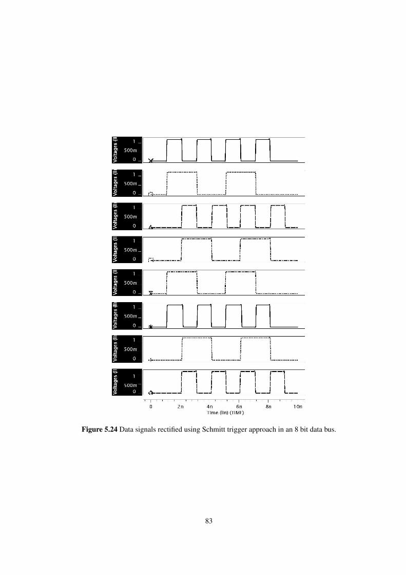
Figure 5.24 Data signals rectified using Schmitt trigger approach in an 8 bit data bus.
83
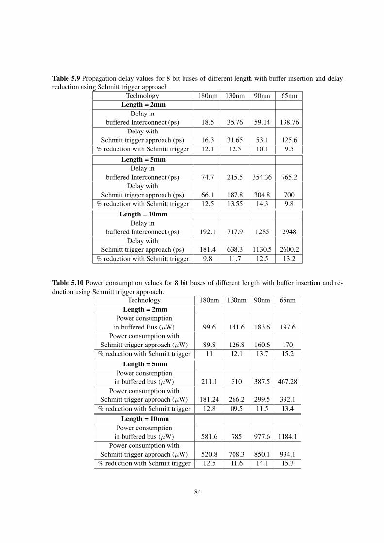
Table 5.9 Propagation delay values for 8 bit buses of different length with buffer insertion and delayreduction using Schmitt trigger approach
Technology 180nm 130nm 90nm 65nmLength = 2mm
Delay inbuffered Interconnect (ps) 18.5 35.76 59.14 138.76
Delay withSchmitt trigger approach (ps) 16.3 31.65 53.1 125.6
% reduction with Schmitt trigger 12.1 12.5 10.1 9.5Length = 5mm
Delay inbuffered Interconnect (ps) 74.7 215.5 354.36 765.2
Delay withSchmitt trigger approach (ps) 66.1 187.8 304.8 700
% reduction with Schmitt trigger 12.5 13.55 14.3 9.8Length = 10mm
Delay inbuffered Interconnect (ps) 192.1 717.9 1285 2948
Delay withSchmitt trigger approach (ps) 181.4 638.3 1130.5 2600.2
% reduction with Schmitt trigger 9.8 11.7 12.5 13.2
Table 5.10 Power consumption values for 8 bit buses of different length with buffer insertion and re-duction using Schmitt trigger approach.
Technology 180nm 130nm 90nm 65nmLength = 2mm
Power consumptionin buffered Bus (µW) 99.6 141.6 183.6 197.6
Power consumption withSchmitt trigger approach (µW) 89.8 126.8 160.6 170
% reduction with Schmitt trigger 11 12.1 13.7 15.2Length = 5mm
Power consumptionin buffered bus (µW) 211.1 310 387.5 467.28
Power consumption withSchmitt trigger approach (µW) 181.24 266.2 299.5 392.1
% reduction with Schmitt trigger 12.8 09.5 11.5 13.4Length = 10mm
Power consumptionin buffered bus (µW) 581.6 785 977.6 1184.1
Power consumption withSchmitt trigger approach (µW) 520.8 708.3 850.1 934.1
% reduction with Schmitt trigger 12.5 11.6 14.1 15.3
84
Chapter 6
Conclusions and Future Work
In this thesis, Schmitt trigger has proposed as an alternate to existing buffer insertion tech-
nique for linear VLSI interconnects for delay, power and noise reduction.
It has been shown that the replacement of buffer with Schmitt trigger helps in reducing delay and power
consumption. Schmitt trigger possesses the property of dual threshold as compared to single threshold
buffer. This property enables the desirable settings of both the voltage thresholds. Thus the signal can
be made to rise/fall faster by keeping the voltage threshold to be lower. Lesser number of transistors
in active mode at the time of switching also results in lesser power consumption thus resulting in more
savings in power consumptions due to the Schmitt trigger as compared to buffer.
It has also been shown that Schmitt trigger helps in reducing cross talk noise in the circuit.
Crosstalk noise is a problem in data buses where close proximity of interconnects results in induced
noise in neighboring lines, which contributes to glitches. It is that there may not be a need for bus
coding techniques for the purpose of crosstalk noise reduction if Schmitt trigger is used for. The extra
hardware which is required in the form of encoder and decoder for bus coding techniques is also not
required. Hence area savings may also be achieved.
6.1 Scope of further work
This thesis focused mainly on linear VLSI interconnects and analyze local, inter- mediate and
global interconnects only. However, since practical interconnects also have tree and mesh structures,
utility of Schmitt trigger in such interconnect structures may be also be explored.
85

Bibliography
[1] Chandrakasan, A. P., S. Sheng, and R. W. Brodersen, “Low-power Digital CMOS Design,” IEEEJournal of Solid State Circuits, pp. 473-484, April 1992.
[2] Proakis and Manolakis, “Digital Signal Processing, Principles, Algorithms, and Applications, 3/e”Prentice Hall of India 2003
[3] P. Saxena and N. Menezes and P. Cocchini and D.A. Kirkpatrick, Repeater scaling and its impacton CAD, IEEE Transactions on Computer-Aided Design, vol. 23, no. 4, pp. 451463, 2004.
[4] P.J. Osler, Placement driven synthesis case studies on two sets of two chips: hierarchical and flat,in Proceedings of International Symposium on Physical Design, San Diego, California, 2004, pp.190197.
[5] Maged M. Ghoneima, Muhammad M. Khellah,“Skewed Repeater Bus: A Low-Power Schemefor On-Chip Buses”, IEEE TRANSACTIONS ON CIRCUITS AND SYSTEMSI: REGULAR PA-PERS, VOL. 55, NO. 7, AUGUST 2008.
[6] Y.I. Ismail and E.G. Friedman, Effects of inductance on the propagation delay and repeater insertionin VLSI circuits, in Proceedings of the Conference on Design Automation, New Orleans, Louisiana,1999, pp. 721724.
[7] Y.I. Ismail, E.G. Friedman, and J.L. Neves, Repeater insertion in tree structured inductive intercon-nect, in Proceedings of the International Conference on Computer-Aided Design, San Jose, Califor-nia, 2001, pp. 420424.
[8] Z. Jiang, S. Hu, J. Hu, Z. Li, and W. Shi, A new RLC buffer insertion algorithm, in Proceedings ofthe International Conference on Computer-Aided Design, San Jose, California, 2006, pp. 553557.
[9] L. P. P. P. van Ginneken, Buffer placement in distributed RC-tree network for minimal Elmore delay,in Proc. Int. Symp. on Circuits and Systems, 1990, pp. 865868.
[10] S. Lin and M. Marek-Sadowska, A fast and efficient algorithm for determining fanout tree in largenetworks, in Proc. of EDAC, Feb 1991, pp. 539544.
86

[11] H. Zhou, D. F. Wong, I. M. Liu, and A. Aziz, Simultaneous routing and buffer insertion withrestrictions on buffer locations, IEEE Trans. on Computer Aided Design of Integrated Circuits andSystems , vol. 19, no. 7, pp. 819824, July 2000.
[12] C. C. N. Chu and D. F. Wong. A quadratic programming approach to simultaneous buffer in-sertion/sizing and wire sizing, IEEE Trans. on Computer Aided Design of Integrated Circuits andSystems, vol. 18, no. 6, pp. 787798, Sept. 1999.
[13] J. Lillis, C. K. Cheng and T.-T. Y. Lin, Optimal wire sizing and buffer insertion for low powerand a generalized delay model, IEEE Trans. Solid-State Circuits, vol. 31, no. 3, pp. 437447, March1996.
[14] C. J. Alpert and A. Devgan. Wire segmenting for improved buffer insertion, in Proc. ACM/IEEEDesign Automation Conf., 1997, pp. 588593.
[15] W. Shi and Z. Li, An O(n log n) time algorithm for optimal buffer insertion, in Proc. ACM/IEEEDesign Aut
[16] W. Shi, Z. Li and C.J. Alpert, Complexity analysis and speedup techniques for optimal bufferinsertion with minimum cost, in Proc. Asia and South Pacific Design Automation Conf., 2004, pp.609614.
[17] S. D. Naffziger et al., “The Implementation of a 2-Core, Multi-Threaded Itanium Family Proces-sor,” IEEE Journal of Solid-State Circuits, Vol. 41, No. 1, pp. 197-209, January 2006.
[18] International Technology Roadmap for Semiconductors. Semiconductor Industry Association,2003.
[19] H. Veendrick, Deep Submicron CMOS ICs - From Basics to ASICs. Deventer, Netherlands:Kluwer, 1998.
[20] H. B. Bakoglu and J. D. Meindl, “Optimal Interconnection Circuits for VLSI,” IEEE Transactionson Electron Devices, Vol. ED-32, No. 5, pp. 903-909, May 1985.
[21] N. Magen et al., “Interconnect-Power Dissipation in a Microprocessor,” Proceedings of the ACMInternational Workshop on System Level Interconnect Prediction, pp. 7-13, February 2004.
[22] F. Chen and D. Gardner, “Influence of Line Dimensions on the Resistance of Cu Interconnections,”IEEE Electron Device Letters, Vol. 19, No. 12, pp. 508-510, December 1998.
[23] A. H. Ajami et al., “Analysis of IR-Drop Scaling with Implications for Deep Submicron P/G Net-work Designs,” Proceedings of the IEEE International Symposium on Quality Electronic Design,pp. 35-40, March 2003.
87
[24] W. Wu and K. Maex, “Studies on Size Effect of Copper Interconnect lines,” Proceedings of Inter-national Conference on Solid-State and Integrated-Circuit Technology, pp. 416-418, October 2001.
[25] A. V. Mezhiba and E. G. Friedman, Power Distribution Networks in High Speed Integrated Cir-cuits. MA: Kluwer Academic Publishers, 2004.
[26] K. Nabors and J. White, “FastCap: A Multipole Accelerated 3-D Capacitance Extraction Pro-gram,” IEEE Transactions on Computer-Aided Design of Integrated Circuits and Systems, Vol. 10,No. 11, pp. 1447-1459, November 1991.
[27] J. H. Chern et al., “Multilevel Metal Capacitance Models for CAD Design Synthesis Systems,”IEEE Electron Device Letters, Vol. 13, No. 1, pp. 32-34, January 1992.
[28] S. Wong, G. Lee, and D. Ma, “Modeling of Interconnect Capacitance, Delay, and Crosstalk inVLSI,” IEEE Transactions on Semiconductor Manufacturing, Vol. 13, No. 1, pp. 108-111, February2000.
[29] K. Gala et al., “Inductance 101: Analysis and Design Issues,” Proceedings of the IEEE/ACMDesign Automation Conference, pp. 329-334, June 2001.
[30] B. Krauter and S. Mehrotra, “Layout Based Frequency Dependent Inductance and Resistance Ex-traction for On-Chip Interconnect Timing Analysis,” Proceedings of the IEEE/ACM Design Au-tomation Conference, pp. 303-308, June 1998.
[31] S. Sim et al., “A Unified RLC Model for High-Speed On-Chip Interconnects,” IEEE Transactionson Electron Devices, Vol. 50, No. 6, pp. 1501-1510, June 2003.
[32] X. Huang et al., “Loop-Based Interconnect Modeling and Optimization Approach for Multigiga-hertz Clock Network Design,” IEEE Journal of Solid-State Circuits, Vol. 38, No. 3, pp. 457-463,March 2003.
[33] S. Yu et al., “Loop-Based Inductance Extraction and Modeling for Multiconductor On-Chip Inter-connects,” IEEE Transactions on Electron Devices, Vol. 53, No. 1, pp. 135-145, January 2006.
[34] A. Mezhiba and E. G. Friedman, “Frequency Characteristics of High Speed Power Distribu-tion Networks,” Analog Integrated Circuits and Signal Processing, Vol. 35, No. 2/3, pp. 207-214,May/June 2003.
[35] T. Dhaene and D. D. Zutter, “Selection of Lumped Element Models for Coupled Lossy Transmis-sion Lines,” IEEE Transactions on Computer-Aided Design of Integrated Circuits and Systems, Vol.11, No. 7, pp. 805-815, July 1992.
[36] S. Sim, K. Lee, and C. Y. Yang, “High-Frequency On-Chip Inductance Model,” IEEE ElectronDevice Letters, Vol. 23, No. 12, pp. 740-742, December 2002.
88
[37] S. Lin and E. Kuh, “Transient Simulation of Lossy Interconnects Based on the Recursive Con-volution Formulation,” IEEE Transactions on Circuits and Systems, Vol. 39, No. 11, pp. 879-892,November 1992.
[38] T. Lin, M. W. Beattie, and L. T. Pileggi, “On the Efficacy of Simplified 2D On-Chip InductanceModels,” Proceedings of the IEEE/ACM Design Automation Conference, pp. 757-762, June 2002.
[39] G. Lei, G. Pan, and B. K. Gilbert, “Examination, Clarification, and Simplification of Modal Decou-pling Method for Multiconductor Transmission Lines,” IEEE Transactions on Microwave Theoryand Techniques, Vol. 43, No. 9, pp. 2090-2100, September 1995.
[40] L. Yin and L. He, “An Efficient Analytical Model of Coupled On-Chip RLC Interconnects,” Pro-ceedings of the IEEE Design Automation Conference Asia and South Pacific, pp. 385-390, January2001.
[41] F. Chang, “Transient Analysis of Lossless Coupled Transmission Lines in a NonhomogeneousDielectric Medium,” IEEE Transactions on Microwave Theory and Techniques, Vol. 18, No. 9, pp.616-626, September 1970.
[42] W. C. Elmore, “The Transient Response of Damped Linear Networks,” Journal of Applied Physics,Vol. 19, pp. 55-63, January 1948.
[43] L. T. Pillage and R. A. Rohrer, “Asymptotic Waveform Evaluation for Timing Analysis,” IEEETransactions on Computer-Aided Design of Integrated Circuits and Systems, Vol. 9, No. 4, pp.352-366, April 1990.
[44] M. A. El-Moursy and E. G. Friedman, “Optimum Wire Shaping of an RLC Interconnect,” Pro-ceedings of the IEEE Midwest Symposium on Circuits and Systems, December 2003.
[45] M. Ghoneima and Y. Ismail, “Optimum Positioning of Interleaved Repeaters in BidirectionalBuses,” IEEE Transactions on Computer-Aided Design of Integrated Circuits and Systems, Vol.24, No. 3, pp. 461-469, March 2005.
[46] F. Anderson, J. S. Wells, and E. Z. Berta, “The Core Clock System on the Next Generation ItaniumMicroprocessor,” Proceedings of the IEEE International Solid-State Circuits Conference, pp. 110-111, February 2002.
[47] L. He and K. M. Lepak, “Simultaneous Shield Insertion and Net ordering for Capacitive andInductive Coupling Minimization,” Proceedings of the ACM International Symposium on PhysicalDesign, pp. 56-61, 2000.
[48] B. Soudan, “The Effects of Swizzling on Inductive and Capacitive Coupling for Wide SignalBusses,” Proceedings of the International Conference on Microelectronics, pp. 300-303, Decem-ber 2003
89
[49] J.J. Cong, K.-S. Leung, “Optimal wiresizing under Elmore delay model”, IEEE Trans. Comput.Aided Design Integrated Circuits Systems 14 (3) (1995) 321336.
[50] P.Sotiriadis and A.Chandrakasan, “Reducing bus delay in sub-micron technology using coding, InProc. of IEEE Asia and South Pacific Design Automation Conf (ASPDAC01),pp 109-114, 2000.
[51] P.Sotiriadis, “Interconnect Modeling and Optimization in Deep Submicron Technologies Disserta-tion Thesis, MIT, May 2002.
[52] Lin Li, Narayanan Vijaykrishnan, Mahmut T. Kandemir, Mary Jane Irwin, “A Crosstalk AwareInterconnect with Variable Cycle Transmission, In Design Automation and Test in Europe (DATE),2004, pp. 102-107.
[53] F.J. Taylor, Digital Filter Design Handbook, Marcel Dekker, Inc., NYC, 1984.
[54] G.K. Ma, and F.J. Taylor, “Multiplier Policies For Digital Signal Processing”, IEEE ASSP Mag.,pp.6- 20, January, 1990.
[55] A.G.Dempster, and M.D.Macleod, “Use of Minimum-Adder Multiplier Blocks in FIR Digital Fil-ters”, IEEE Trans. Circuits Syst. 11, vol. 42, no. 9, pp. 569-577, Sept, 1995.
[56] Reza Hashemian “A New Method for conversion of a 2s complement to Canonic Sign Digit Num-ber System and its Representation, in Proceedings of Asilomar Conference on Signals, Systems andComputers, pp. 904-907., 1997.
[57] Dejhan, K., Tooprakai, P., Rerkmaneewan, T. Soonyeekan, C., “A high-speed direct bootstrappedCMOS Schmitt trigger circuit” ,Semiconductor Electronics, 2004. ICSE 2004. IEEE InternationalConference, 7-9 December 2004.
[58] O.H. Schmitt to H.R. Lang, Nov. 25, 1937, O.H. Schmitt Papers, University Archives, Universityof Minnesota, Minneapolis, MN, Box SF114.
[59] O.H. Schmitt, A thermionic trigger, J. Sci. Instrum., vol. 15, no. 1, pp. 2426.
[60] B. Hart, Picturing Schmitts trigger, Electron. World, vol. 105, no. 1764, pp. 10401046, 1999.
[61] P. R. Gray and R. G. Meyer, “Analysis and Design of Analog Integrated circuits”, 2nd edition,New York: Wiley, 1984.
[62] P. Sotiriadis and A. Chandrakasan “Low power Coding Techniques Considering Inter wire ca-pacitances, In Proc. Of IEEE Conferences on Custom Integrated Circuits (CICC00), pp 507-510,2000.
[63] M.R Stan and W.P Burleson, “Bus Invert Coding for Low Power I/O, IEEE Transactions VLSIsystems, pp 49-58, March 1995.
90
[64] P. Sotiriadis, “Interconnect Modeling and Optimization in Deep Submicron Technologies, Disser-tation Thesis, Massachusetts Institute of Technology, May 2002.
[65] Yan Zhang et al, “Odd/Even bus invert with two phase transfer for buses with coupling, Proceed-ings of ISPLED 02, pp 80-83, August 12-14, Monterey, CA, USA.
[66] Jayapreetha Natesan and Damu Radhakrishnan, “Shift Invert coding (SINV) for low power VLSI,Proceedings of EUROMICRO Systems on Digital System Design (DSD04), pp 190-194, 2004.
[67] J.V.R Ravindra, K.S. Sainarayanan, M.B. Srinivas, “A novel bus coding technique for low powerdata transmission, IEEE symposium on VLSI design and test conference (VDAT-2005), pp 263-266,August 2005.
[68] P. Ghosh, R. Mangaser, K. Rose, “Interconnect-dominated VLSI design”, Proceedings of the Con-ference on Advanced Research, March 1999, pp. 114122.
[69] Semiconductor Industry Association, The National Technology Roadmap for Semiconductors -1997 Edition.
[70] M. T. Bohr, Proc. IEEE International Electron Devices Meeting, p. 241, 1995.
[71] E. E. Davidson, IEEE Micro, 18/4, p. 33, 1998.
91