Embed Size (px)
Citation preview

HAL Id: hal-01388299https://hal.archives-ouvertes.fr/hal-01388299
Submitted on 18 Nov 2019
HAL is a multi-disciplinary open accessarchive for the deposit and dissemination of sci-entific research documents, whether they are pub-lished or not. The documents may come fromteaching and research institutions in France orabroad, or from public or private research centers.
L’archive ouverte pluridisciplinaire HAL, estdestinée au dépôt et à la diffusion de documentsscientifiques de niveau recherche, publiés ou non,émanant des établissements d’enseignement et derecherche français ou étrangers, des laboratoirespublics ou privés.
A Novel approach to Extract the Thyristor DesignParameters for Designing of Power Electronic Systems
Atef Jedidi, Hatem Garrab, Hervé Morel, Kamel Besbes
To cite this version:Atef Jedidi, Hatem Garrab, Hervé Morel, Kamel Besbes. A Novel approach to Extract the ThyristorDesign Parameters for Designing of Power Electronic Systems. IEEE Transactions on Industrial Elec-tronics, Institute of Electrical and Electronics Engineers, 2015, 62 (4), �10.1109/TIE.2014.2356440�.�hal-01388299�
1
Abstract—Accurate simulation is an essential task in designing of integrated power systems to predict their electrical behavior. Thus, a very good description of their wiring circuits is required, and the availability of accurate models of power semiconductor devices and associated design parameters is crucial. This paper focuses on a novel extraction approach of design parameters for a 1-D finite-element-method model of the thyristor. These design parameters are also essential for physics-based analytical models. This paper presents an extraction procedure of the main design parameters of an ultrafast thyristor: the effective area of the device, the ambipolar lifetime, the doping concentration and width of the low-doped base region, and the doping concentration and width of the gate region. The extraction procedure of the thyristor design parameter is based on a comparative computation between simulation and experimental results, taking into account the physics of the component. Measurements are carried out on a sophisticated test circuit, which must be modeled with a sufficient accuracy. This paper details the parame- ter extraction procedure. Various electrothermal simulation results about the thyristor under test, using the extracted values of design parameters, show good agreement with experiment and confirm the validity of the presented extrac- tion procedure.
Index Terms— Modeling, Finite Element Method (FEM),
Thyristors, Simulation.
I. INTRODUCTION
Hyristors and gate turn-off thyristors (GTOs) continue to
be used in power electronic applications particularly for
high power application [1]–[6]. Thyristors are also available
as new silicon carbide devices with strong capabilities [7]–
[9]. However, silicon devices are further available at lower
cost. Therefore, the availability of thyristor models is highly
recommended for the analysis and design of power electronic
systems, including thyristors and even GTO. Modeling and
Manuscript received February 21, 2014; revised May 10, 2014;
accepted July 29, 2014. Copyright (c) 2014 IEEE. Personal use of this material is permitted.
However, permission to use this material for any other purposes must be obtained from the IEEE by sending a request to [email protected].
A. Jedidi, H. Garrab, and K. Besbes are with the Microelectronics and Instrumentation Laboratory (LR13ES12), Department of Physics, Science Faculty of Monastir, University of Monastir, 5000 Monastir, Tunisia (e-mail: [email protected]; [email protected]; kamel.besbes@ fsm.rnu.tn).
H. Morel is with the Ampere Laboratory, University of Lyon [Insti- tut National des Sciences Appliquées (INSA)], Centre National de la Recherche Scientifique (CNRS), 69621 Villeurbanne, France (e-mail: [email protected]).
.
simulation are an essential part of the design flow of power
electronic systems. The modeling is used to consider
nonmeasurable amounts of real devices, to optimize the
realization cost and to increase the reliability of designed
circuits. A precise description of power system behavior
requires the availability of accurate component models. The
validity of the semiconductor device models depends not only
on semiconductor equations but also on device design
parameters, i.e., the structure definition. Since it is difficult to
obtain these parameters directly from the manufacturers, the
extraction of these parameters may be based on reverse
engineering techniques, but it remains a sensitive and a
destructive task. There is therefore great interest in the
development of nondestructive extraction and appropriate
methods to obtain accurate models of power devices [10]–
[15]. This paper describes a step-by-step extraction procedure
to identify the main design parameters of a thyristor. This is a
first step toward the design and optimization of power
electronic systems using thyristors and GTO based on silicon
or silicon carbide materials dedicated to transportation systems
and power distribution and transmission of electricity.
Section II presents a state-of-the-art of the thyristor
modeling and the selected modeling approach. Section III
presents the model of the circuit used for the comparison
between simulation and experiments. Section IV presents the
extraction procedure. Section V presents some preliminary
results and the analysis of the validity domain of the obtained
parameters. This paper finishes by some conclusions.
II. THYRISTOR MODELING
Given the complexity of physical phenomena that governs
thyristor operation, published model accuracy for such device
is usually weak [16]–[20]. The SPICE model in [16] is not
accurate since it does not consider the high-level injection
phenomena in the thyristor epitaxial layer. Literature reports
also models using lumped-charge techniques [18]–[20]. These
models use localized charge method to get a pretty accurate
description of the charge behavior in the component base
region. These models as those based on finite-element
methods (FEMs) depend on device design parameters.
The FEM is one of the most accurate approaches in power
devices modeling. In this paper, the FEM is selected for
thyristor modeling. The 2-D basic structure of a vertical power
thyristor is presented in Fig. 1. It is based on a lightly doped
N-type
A Novel Approach to Extract the Thyristor Design Parameters for Designing of Power
Electronic Systems Atef Jedidi, Hatem Garrab, Member, IEEE, Hervé Morel, Senior Member, IEEE, and Kamel
Besbes, Member, IEEE
T
2
(a)
Base
l o g
Depth,xPN+
gate
Cat
hod
e
An
ode
N-P+XJA
XJK
Ng
Wg
NB
WB
(b)
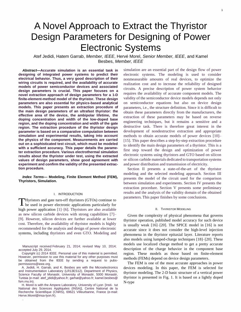
Fig. 1. Simplified 2-D architecture for the thyristor. (a) 2-D structure of
a meshed thyristor. (b) Thyristor doping profile according a vertical
section from cathode to anode as mentioned in (a)
TABLE I.
THYRISTOR DESIGN PARAMETERS
Symbol Definition
WB (µm) Width of the lightly doped base region of thyristor
NB (cm-3) Doping of the lightly doped base region of thyristor
Wg (µm) Width of the thyristor gate region
Ng (cm-3) Doping concentration of the thyristor gate region
A (mm2) Thyristor effective area
τ (µs) Thyristor ambipolar lifetime
XJA(µm) Depth of the anode-base junction
XJK(µm) Depth of the cathode-gate junction
N+ (cm-3) Doping concentration of the thyristor cathode region
P+ (cm-3) Doping concentration of the thyristor anode region
layer (epitaxy or substrate), whose optimized for the blocking
voltage of the device. The cathode region, the P-gate area and
the anode region contacts, are respectively established on the
front side and the back side of the wafer. Table I gives the list
of the thyristor design parameters.
The main design parameters that characterize the arbitrary 1-D
technological architecture of thyristor are shown in Fig. 1(b).
Identification of the N+ and P
+ regions is behind the scope of
this paper since their impacts are of second order on the
thyristor transient behavior except at very high current level
where the lateral regions control the carrier injection [21].
The secondary design parameters of thyristor XJA, XJK, N+
and P+ are set arbitrarily as follows XJA= 40 µm, XJK= 2 µm,
P+= 10
20cm
-3 and N
+= 10
20cm
-3. These values are of the same
order as those of commercial device technologies.
Using the graphical tool, MDRAW-ISE TCAD [22], the
thyristor 2-D architecture presented in Fig. 1(a) is
implemented in FEM simulator DESSIS-ISE TCAD [23]. A
meshing tool is after used to produce the necessary data such
as: geometric data structure and doping profile of the
component which will be used by the simulator, DESSIS-ISE
TCAD. A fine meshing is performed in gate-base, cathode-
gate and base-anode junctions and electrode contacts.
III. CIRCUIT MODEL
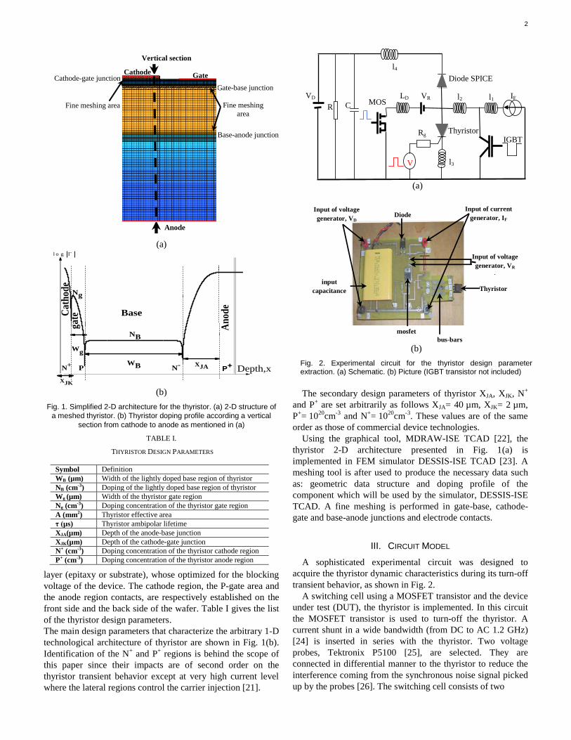
A sophisticated experimental circuit was designed to
acquire the thyristor dynamic characteristics during its turn-off
transient behavior, as shown in Fig. 2.
A switching cell using a MOSFET transistor and the device
under test (DUT), the thyristor is implemented. In this circuit
the MOSFET transistor is used to turn-off the thyristor. A
current shunt in a wide bandwidth (from DC to AC 1.2 GHz)
[24] is inserted in series with the thyristor. Two voltage
probes, Tektronix P5100 [25], are selected. They are
connected in differential manner to the thyristor to reduce the
interference coming from the synchronous noise signal picked
up by the probes [26]. The switching cell consists of two
(a)
(b)
Fig. 2. Experimental circuit for the thyristor design parameter extraction. (a) Schematic. (b) Picture (IGBT transistor not included)
IGBT
VD
Thyristor
MOS
Diode SPICE
LD
V
VR
Rg
l3
l4
C R
l2 l1 IF
Input of voltage
generator, VD
Thyristor
Input of voltage
generator, VR
Diode Input of current
generator, IF
bus-bars
mosfet
input
capacitance
Anode
Fine meshing
area
Base-anode junction
Gate-base junction
Cathode Gate Cathode-gate junction
Fine meshing area
Vertical section

3
-90,0µ 0,0 90,0µ
0
5
10
15
IGBT gate pulse
IGBT gate pulse
MOSFET gate pulseThyristor gate pulse
Vo
lta
ge[V
]
Time[s]
Fig. 3. Experimental control signal for IGBT, MOSFET and the thyristor gate.
voltage generators, a current generator, a MOSFET transistor,
an insulated-gate bipolar transistor (IGBT), a p-i-n diode and a
drive circuit, including a microcontroller delivering three
synchronized pulses. These pulses are after amplified. These
three obtained pulses are applied to the MOSFET transistor,
the IGBT transistor and the DUT. The control timing diagram
is shown in Fig. 3.
The IGBT transistor (MUP304) is turned-off only several
tens of microsecond every hundreds of milliseconds and it is
turned-on most of the time hence shorting the current source.
The IGBT transistor enables to ensure the most part of power
dissipation. Therefore, the self-heating of thyristor and
MOSFET is avoided.
The experimental circuit is designed to give the best
comparison condition between the measurements and the
simulation obtained with the circuit model in Fig. 2. Hence,
the experimental circuit includes two inductors (I1, air-
inductor) and (I2, core-inductor) in series with the current
source, whose purpose to stabilize its current IF during
switching. Polypropylene and ceramic capacitance is added in
parallel with the voltage source to stabilize the applied
voltage, VD. The voltage source is not reversible in current, so
resistance is added in parallel to the voltage generator VD to
dissipate the average energy returned to the source and allows
proper regulation of the voltage source. The IGBT transistor
shorts the current source when a pulse is applied to its gate
and the IF current is flowing through the IGBT. However,
when the IGBT transistor is turned-off, the current flow in the
PiN diode and the DUT is blocked and forward biased by the
VD voltage. Once the thyristor gate is activated, the conduction
process of component is triggered. Then, a pulse is applied to
the MOSFET gate that turns-on and enforces the thyristor to
turn-off in a recovery process. The duration of the pulse that
switches the MOSFET should be long enough to avoid
immediate turn-on of the thyristor under test at reapplication
of the forward voltage. This is related to the TQ of the
thyristor. Once the MOSFET is turned-on, the thyristor is
reverse biased by the voltage generator (VR). Thereby, the
stored charge in the thyristor base during its conduction phase
will be evacuated and the reverse recovery phenomenon of
thyristor starts. Experimental current and voltage waveforms
0,0 1,0µ 2,0µ 3,0µ 4,0µ
-30
-20
-10
0
600,0n 1,2µ 1,8µ
-30
-20
-10
0
Current slope during
the second recovery phase
diR/dt
diF/dt
t3t2t1
IRM
I th
yri
sto
r[A
]
Time[s]
zoom
t4t3t2t1
tr2
1% of IRM
I F=
0 A
IRM
trr
tr1
I th
yri
sto
r[A
]
Time[s]
0,0 1,0µ 2,0µ 3,0µ 4,0µ
-100
-50
0
600,0n 1,2µ 1,8µ
-100
-50
0
t1 t2 t3
VRM
Vth
yri
sto
r[V
]
Time[s]
zoom
t1 t2 t3t4
VRM
Vth
yris
tor[V
]
Time[s] Fig. 4. Experimental current and voltage waveform across the Thyristor
during its turn-off phase (IF = 2A and VR = 100V)
TABLE II.
MAIN SWITCHING PARAMETERS OF THYRISTOR
Symbol Definition
IRM(A) Maximum reverse current of thyristor
VRM(V) Maximum reverse voltage of thyristor
tr1 (µs) The first recovery time associated to the stored charge
recovery in the thyristor base
tr2 (µs) the second reverse recovery time associated to recovery
of the stored charge amount remaining in the thyristor
gate and base region
trr (µs) = tr1+ tr2 Total reverse recovery time of thyristor
across the thyristor during its turn-off phase are shown in Fig.
4. On these transient behavior characteristics, main switching
parameters of thyristor are defined and they are illustrated in
Table II.
Main switching parameters will be useful for the extraction
procedure since they characterize the simulated and
experimental waveforms of current and voltage across the
component during its turn-off phase.
During the thyristor conduction phase, a high-level injection
regime is established in the central region of the device. As for
the p-i-n diode, the integration of continuity equations for
holes and electrons gives the amount of the stored charge, i.e.,
4
Q0 = τ· I. To turn off the thyristor, all the stored charge should
be evacuated. However, during the device turn-off phase, one
part of this stored charge is recombined inside the component.
The remaining amount called recovery charge is evacuated due
to the reverse current. The evacuation process of this recovery
charge is decomposed into two parts. Initially, a portion of this
charge Q1 that has been already stored in the thyristor base
region is recovered from instant t1 to t3. From t1 to t2, the
anode current decreases according to a constant slope dIF /dt.
This slope is essentially determined by values of circuit
inductors crossed by the current and value of the reverse applied
voltage VR across the thyristor. Meanwhile, from t2 to t3, the
anode current increases according to a constant slope dIR/dt.
For instant t3, as mentioned on the current waveform in Fig. 4,
the current slope dIR/dt changes suddenly in terms of value,
and the current magnitude is about 10% of the maximum
reverse current, IRM, and the space charge region is extended
on the maximal position. The remaining amount of charge
Q2 that includes charges stored in the component gate region
is evacuated from instant t3 to t4. At instant t4, the current
magnitude through the thyristor is about 1% of IRM.
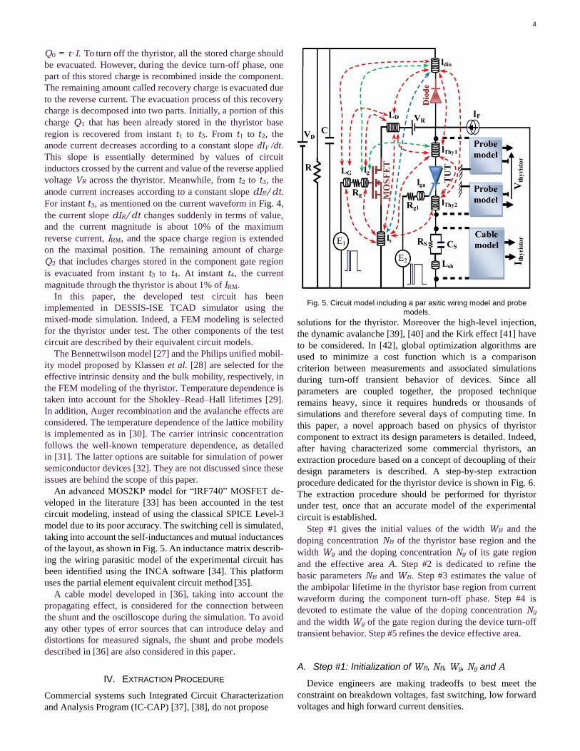
In this paper, the developed test circuit has been
implemented in DESSIS-ISE TCAD simulator using the
mixed-mode simulation. Indeed, a FEM modeling is selected
for the thyristor under test. The other components of the test
circuit are described by their equivalent circuit models.
The Bennettwilson model [27] and the Philips unified mobil-
ity model proposed by Klassen et al. [28] are selected for the
effective intrinsic density and the bulk mobility, respectively, in
the FEM modeling of the thyristor. Temperature dependence is
taken into account for the Shokley–Read–Hall lifetimes [29].
In addition, Auger recombination and the avalanche effects are
considered. The temperature dependence of the lattice mobility
is implemented as in [30]. The carrier intrinsic concentration
follows the well-known temperature dependence, as detailed
in [31]. The latter options are suitable for simulation of power
semiconductor devices [32]. They are not discussed since these
issues are behind the scope of this paper.
An advanced MOS2KP model for “IRF740” MOSFET de-
veloped in the literature [33] has been accounted in the test
circuit modeling, instead of using the classical SPICE Level-3
model due to its poor accuracy. The switching cell is simulated,
taking into account the self-inductances and mutual inductances
of the layout, as shown in Fig. 5. An inductance matrix describ-
ing the wiring parasitic model of the experimental circuit has
been identified using the INCA software [34]. This platform
uses the partial element equivalent circuit method [35].
A cable model developed in [36], taking into account the
propagating effect, is considered for the connection between
the shunt and the oscilloscope during the simulation. To avoid
any other types of error sources that can introduce delay and
distortions for measured signals, the shunt and probe models
described in [36] are also considered in this paper.
IV. EXTRACTION PROCEDURE
Commercial systems such Integrated Circuit Characterization
and Analysis Program (IC-CAP) [37], [38], do not propose
Fig. 5. Circuit model including a par asitic wiring model and probe
models.
solutions for the thyristor. Moreover the high-level injection,
the dynamic avalanche [39], [40] and the Kirk effect [41] have
to be considered. In [42], global optimization algorithms are
used to minimize a cost function which is a comparison
criterion between measurements and associated simulations
during turn-off transient behavior of devices. Since all
parameters are coupled together, the proposed technique
remains heavy, since it requires hundreds or thousands of
simulations and therefore several days of computing time. In
this paper, a novel approach based on physics of thyristor
component to extract its design parameters is detailed. Indeed,
after having characterized some commercial thyristors, an
extraction procedure based on a concept of decoupling of their
design parameters is described. A step-by-step extraction
procedure dedicated for the thyristor device is shown in Fig. 6.
The extraction procedure should be performed for thyristor
under test, once that an accurate model of the experimental
circuit is established.
Step #1 gives the initial values of the width WB and the
doping concentration NB of the thyristor base region and the
width Wg and the doping concentration Ng of its gate region
and the effective area A. Step #2 is dedicated to refine the
basic parameters NB and WB. Step #3 estimates the value of
the ambipolar lifetime in the thyristor base region from current
waveform during the component turn-off phase. Step #4 is
devoted to estimate the value of the doping concentration Ng
and the width Wg of the gate region during the device turn-off
transient behavior. Step #5 refines the device effective area.
A. Step #1: Initialization of WB, NB, Wg, Ng and A
Device engineers are making tradeoffs to best meet the
constraint on breakdown voltages, fast switching, low forward
voltages and high forward current densities.

5
Fig. 6. Extraction procedure algorithm.
The breakdown voltage is related to NB and WB of the
lightly doped region of the device [37] where the electric field
and the space charge region will extend when the component
is reverse biased. The study of edge terminations of thyristors
is outside the scope of this paper, and the breakdown voltage
is assumed to be mainly determined by the device volume
properties. The thyristor model shown in Fig.1 is simulated in
the circuit of Fig. 7 (a), for various values of NB and WB.
In Fig. 7 (b), it is noted that the device breakdown voltage
increases as the doping level of the lightly doped layer
decreases and when its thickness increases. To optimize the
resistance of the lightly doped layer, a good tradeoff between a
low forward voltage drop and a high breakdown voltage
should be found. This tradeoff corresponds to a parameter
couple (WB and NB) located just in the knee region [31], [43],
as mentioned in Fig. 7 (b).
(a)
1E12 1E13 1E14 1E15 1E1610
2
103
104
The Knee region
NB[cm-3]
WB = 20 µm
WB = 10 µm
WB = 30 µm
WB = 50 µm
WB = 70 µm
WB = 100 µm
WB = 140 µm
WB = 200 µm
WB = 300 µm
Brea
kd
ow
n V
olt
ag
e:V
BR
[V]
(b)
Fig.7. (a) Simulation circuit for breakdown voltage estimation. (b)
Estimation breakdown voltage using simplified 2-D model in Fig.1
For setting the WB and NB parameters, the smallest
thickness and the highest doping of the thyristor base region in
the knee region are selected. From a visual inspection, initial
values of WB and NB are selected. The estimation of the initial
value of the effective area of the component can be deduced
from the current density usually given by the manufacturer
according to the law given by Aop = IF / JN, where JN is the
typical density of current (from 100 to 300 A/cm2) and Aop is
the optimal effective area of the device.
For initialization of parameter values of the thyristor gate
layer, Wg is set to a smaller value than WB and Ng is set to a
higher value than NB.
B. Step #2: First Refinement of WB and NB
The refinement of these two parameters is performed by
matching experimental and simulated reverse static
characteristics. Using a Tektronix 371A high-power curve
tracer, experimental I-V curves of thyristors under test are
acquired. The simulation results are obtained through
numerical simulation using DESSIS-ISE TCAD simulator in
quasi-stationary mode. After having initiated a series of
simulation by varying the WB and NB parameter values, a
good agreement is obtained between the experimental and
simulated waveforms of the breakdown voltages of three
commercial thyristors 2N6508G, 2N6397G and BT153 as
illustrated in Fig. 8(b). The estimated parameters for each
component are given in Fig. 8(a).
Delivery of design parameter set
and validity domain.
No
Step #4: Estimation of Ng and Wg from the experimental current
waveform during the reverse recovery times, tr1 and tr2 of thyristor
No
Creation of validity maps for switching parameters.
Step#1: Initialization of WB, NB, Wg, Ng and A.
Step #2: Estimation of WB and NB from the
experimental breakdown voltage of thyristor
Yes
Step #3: Estimation of the ambipolar lifetime, τ from the
experimental current waveform during the thyristor turn-off
transient behavior
Yes
A good agreement between the
experimental and simulated breakdown
voltage?
No
Step #5: Estimation of the effective area from the experimental
maximum reverse voltage, VRM of thyristor
A good agreement between experimental and simulated current waveforms during
its turn-off transient behavior?
Satisfying accuracy of validity maps?
Yes
Yes
No
A good agreement between the
experimental and simulated breakdown
voltage?
0V
-10-4
V
Thyristor E VR

6
1E14 1E15
400
600
800
1000
1200
1400
NB[cm-3]
2N6508G
(NB=2,4X10
14cm
-3,W
B=40µm)
BT153
(NB=4,2X10
14cm
-3,W
B=33µm)
2N6397G
(NB=6,2X10
14cm
-3,W
B=24µm)
50µm
30µm
20µm
Bre
ak
do
wn
Vo
lta
ge:
VB
R[V
]
(a)
0 100 200 300 400 500 6000,0
0,5
1,0
1,5
2,0
2,5
3,0
3,5
4,0
4,5 Experiment
Simulation
BT
15
3
2N
65
08
G
2N
63
97
G
I th
yri
sto
r[A
]
VBR[V] (b)
Fig.8 . Refinement of WB and NB based on reverse-bias I-V curve. (a) Refined values of WB and NB. (b) Simulated and experimental breakdown voltage for three commercial devices.
C. Step #3: Estimation of τ and refinement of WB and
NB
First, the ambipolar lifetime is a fundamental parameter for
industry of power semiconductor devices. This parameter
significantly affects the direct and transient behavior of power
devices and, in particular, their switching speed. Device design
engineering creates deep recombination centers by instance by
diffusion of heavy metals (Au or Pt) in the lightly doped region,
to optimize and to control the ambipolar lifetime [44]. During
turn-off transient behavior of the thyristor, stored charge in the
lightly doped region, while the component is turned on, is
evacuated. This amount of stored charge in the base and gate
regions is related to the ambipolar lifetime. Several simulations
are performed to predict the influence of the ambipolar lifetime
variation on current and voltage waveforms during the thyristor
turn-off switching. It is noted that the switching parameters
IRM and the reverse recovery time trr and, in particular, the
first reverse recovery time tr1 are very sensitive to change of
the ambipolar lifetime. Hence, by varying the ambipolar
lifetime value, its estimation is obtained by matching simulated
and experimental current waveforms, during turn-off transient
behavior of the thyristor, and using the DESSIS-ISE TCAD
simulator. For this estimated parameter, practically the same
value of reverse current, IRM and reverse recovery time, tr1 is
obtained for simulated and experimental current waveforms.
Since they are also related to the stored charge during the
component turn-on state, NB and WB should be adjusted again.
Step#2 is repeated for the sake of coherence with the latest
parameter estimated of τ and the breakdown voltage of the
component is respected.
D. Step #4: Estimation of Wg and Ng of the gate region
Several simulations using the DESSIS-ISE TCAD simulator
are performed to observe the influence of width of the gate
region Wg and its doping concentration Ng on current and
voltage waveforms during the thyristor turn-off phase. Influ-
ence of these two parameters occurs during the second phase
of evacuation of the remaining amount of stored charge in the
thyristor gate region. A change of Ng value has a remarkable
influence first on the second recovery time tr2 and second on
the current magnitude through the thyristor at instant t3, as
mentioned in Fig. 4. However, a variation of Wg affects the
reverse recovery time tr2, while keeping practically the same
current amplitude for the instant t3. The estimation of the
value of doping concentration Ng is obtained by matching the
simulated and experimental value of the anode current
magnitude at instant t3. Afterward, Wg is varied until
matching the experimental and simulated value of tr2. For these
later estimated parameters Wg and Ng, a good agreement is
found between experimental and simulated current waveforms
during the thyristor turn-off transient behavior. For this later
estimated doping concentration Ng, the anode current
magnitude for instant t3 corresponds practically to 10% of
IRM. The NB and WB settings must be adjusted again, since they
are related to the stored charge. Step #2 should be started again
to have a good agreement between the simulated and
experimental current waveforms and the same breakdown
voltage of the thyristor under test in simulation and
experiment. Step #3 should be also repeated by the way since
the ambipolar lifetime is also related to the stored charge.
E. Step #5: Estimation of the effective area, A
At the end of the thyristor reverse recovery, the turn-off
experimental voltage waveform presents oscillations due to
interactions between the silicon-controlled rectifier extended
across anode–base and cathode–gate junctions and the external
circuit. During the recovery process, the variation of the device
effective area has, therefore, a great effect, particularly on the
magnitude of the first oscillation of the voltage waveform,
corresponding to the maximum reverse voltage VRM. Thus,
estimation of the thyristor effective area A is obtained by
matching the simulated and experimental value of VRM. This
latter estimated value of A corresponds to a good agreement
between simulated and experimental voltage waveforms across
the component during its turn-off switching. Since the stored
charge inside the lightly doped region of the thyristor, when it is
turned on, is also related to its effective area, the optimization of
the ambipolar lifetime procedure must be restarted again with
the estimated value of the effective area. Therefore, the opti-
mization step of NB and WB values must be performed again to

7
TABLE III.
COMPARISON OF SWITCHING PARAMETER VALUES
FOR A 2N6508G THYRISTOR
Simulation Experiment Error
IRM(A) -33 -32,6 1,2%
VRM(V) -108 -111,5 3,1%
trr (µs) 5,4 5,32 1,3%
0,0 1,0µ 2,0µ 3,0µ
-30
-20
-10
0
Experiment
Simulation
Thyristor: 2N6508G
I th
yris
tor[A
]
Time[s] (a)
0,0 1,0µ 2,0µ 3,0µ
-105
-70
-35
0
Experiment
Simulation
Thyristor: 2N6508G
Vth
yri
sto
r[V
]
Time[s] (b)
Fig. 9. Comparison of experimental and simulation results. (a) Current
waveforms. (b) Voltage waveforms.
respect the measured breakdown voltage of the thyristor under
test. Steps #2 and #3 are also repeated.
The step-by-step extraction procedure is adopted and per-
formed for three commercial thyristors under test. Table III
reports the experimental and simulated values of the main
switching parameters IRM, VRM, and trr of the 2N6508G
thyristor for the following operation conditions: IF = 2 A and
VR = 100 V.
A good agreement is observed between experimental and
simulated waveforms, as shown in Fig. 9. This agreement is
slightly degraded after the high dv/dt and before steady state.
Indeed, some oscillations appear in the experimental voltage
waveform during this slot time. This disagreement may be due
to inaccuracy in the representation of inductive and capacitive
parasitic elements and inaccuracy of the component geometry.
The 3-D effect not supported in our work for the FEM modeling
of the thyristor could be also a cause of this disagreement. This
TABLE IV.
OPTIMAL DESIGN PARAMETER SET
FOR THREE COMMERCIAL THYRISTORS
Thyristor 2N6508G 2N6397G BT153
NB (cm-3) 2,3.1014 6.1014 4.1014
WB (µm) 41 23 32
Ng (cm-3) 1,95.1017 1,15.1017 1,4.1017
Wg (µm) 4,2 6 5
A (mm2) 35 28 33,6
τ (µs) 9 5 8
disagreement has no important effects on the extracted design
parameters.
Extracted design parameters for three commercial thyristors
under test are shown in Table IV.
To additionally validate the extracted effective area of the
thyristor under test, its current density J = IN /A is com-
puted, where IN is its nominal current, and A is its ef-
fective area. For example, for the 2N6397G thyristor, J =
5 A/28 mm2 = 178.6 A/cm2. This value is in good agreement
with the typical value mentioned previously (100 A/cm2 <
JN < 300 A/cm2). Therefore, the effective area of the com-
ponent fits well with its physical size.
V. VALIDITY DOMAIN
The validity of extracted design parameters of the thyristor
under test is examined by an electrothermal simulation study.
Indeed, a comparative study is performed between experimen-
tal and simulated waveforms of current and voltage across the
device 2N6397G for high operating temperatures. Inside the
switching cell circuit, the thyristor operating temperature is
controlled by an air flow using a thermal stream system model
TP041AH, where the temperature is monitored by a
thermocouple and controlled by a microprocessor that regulates
the air stream temperature with high stability and accuracy. Fig.
10 pictures experimental current and voltage waveforms for
various operating temperatures. From this figure, it is noted that
the switching parameters IRM and trr increase with the thyristor
operating temperature, while VRM decreases with To. To
compare these experimental data to simulation results, the
electrothermal simulation mode is selected for thyristor
modeling using the DESSIS-ISE TCAD simulator, taking into
account their extracted design parameters. An excellent agree-
ment is obtained between experimental and simulated current
and voltage waveforms for various operating temperatures
during the thyristor turn-off transient behavior, as shown in Fig.
10.
The extracted design parameters of 2N6397G, 2N6508G,
and BT153 devices shown in Table II are used in the
electrothermal simulation. To compare the experimental data
to simulation results for these three commercial thyristors, the
simulated and experimental values of the main switching
parameters are selected to be compared since they characterize
the turn-off waveforms. Fig. 11 compares several simulation
and experimental results about the main switching parameters
for the three commercial thyristors. A good agreement is found
between simulated and experimental results since error
between them is less than 2%.

8
500,0n 1,0µ 1,5µ 2,0µ 2,5µ 3,0µ
-30
-20
-10
0
Experiment
Simulation
2N6397G
200,0n 300,0n 400,0n 500,0n 600,0n 700,0n
-30
-20
-10
0 T0=300K
T0=380K
T0=420K
Experiment
Simulation
2N6397GI t
hyri
sto
r[A
]
Time[s]
Zoom
T0=380K
T0=300K
T0=420K
I th
yri
sto
r[A
]
Time[s] (a)
500,0n 1,0µ 1,5µ 2,0µ 2,5µ 3,0µ
-100
-50
0
200,0n 300,0n 400,0n 500,0n 600,0n 700,0n
-100
-50
0 Experiment
Simulation
2N6397G
T0=380KT0=300K
T0=420K
Vth
yri
sto
r [V
]
Time[s]
Experiment
Simulation
2N6397G
Zoom
T0=380KT0=300K
T0=420K
Vth
yri
sto
r[V
]
Time[s] (b)
Fig. 10. Comparison of experimental and simulation results at various operating temperatures. (a) Current waveforms. (b) Voltage waveforms.
All extracted design parameters of various thyristors under
test are mainly deduced from current and voltage waveforms
across components during their turn-off transient behavior for
operating conditions (IF = 2 A and VR = 100 V). To further
highlight validity of extracted design parameters, a
comparative study between experimental and simulated
switching parameter values versus IF current and VR voltage
should be established. The error evolution between simulated
and experimental value of trr, VRM and IRM parameters versus
IF current and VR voltage are dressed in maps on Fig. 12.
Thereby the validity maps of thyristor model including
extracted parameters could be discussed. An error less than
6.8 % is observed in the VRM validity map. However trr and
IRM validity maps indicate an error less than 4.8%.
Validity maps of VRM, IRM and trr demonstrates the validity
of the extraction procedure and the extracted design
parameters of thyristor under test since the error rate between
simulated and experimental values of switching parameters
remain acceptable. Some perturbations of measurement are
found for high current, IF and for high voltage VR. These
perturbations constitutes the technical limitations of the work
bench which explain why the IF current and the VR voltage did
not exceed respectively 5A and 200V in the validity maps.
These technical limitations do not prevent the extraction of the
thyristor design parameters.
280 300 320 340 360 380 400 420
-36
-34
-32
-30
-28
-26
BT153
2N6397G
2N6508G
I RM
[A]
Operating temperature[K]
Experiment
Simulation
(a)
280 300 320 340 360 380 400 420-140
-130
-120
-110
-100
Experiment
Simulation
2N6508G
2N6397G
BT153
VR
M[V
]
Operating temperature[K] (b)
300 320 340 360 380 400 420
4
5
6
7
8
9
2N6397G
BT153
2N6508G Experiment
Simulation
t rr[µ
s]
Operating temperature[K] (c)
Fig. 11. Experimental and simulated of main switching parameters
versus the operating temperature for three commercial thyristors: (a)
IRM, (b) VRM and (c) trr.
VI. CONCLUSION
We have shown that it is possible to accurately extract the
main design parameters of thyristor, using a novel approach
based on concept of decoupling of their design parameters,
taking into account the physics of the component. On the one

9
6,1%
5,6%
5,1%4,6%
4,1%
3,6%
4,1%
1 2 3 4 5
60
80
100
120
140
160
180
200
IF[A]
VR
[V] 3,1%
3,6%
4,1%
4,6%
5,1%
5,6%
6,1%
6,6%
6,8%
(a)
4,5%4,1%
3,8%
3,4%3,1%
2,7%2,4%
1 2 3 4 5
60
80
100
120
140
160
180
200
IF[A]
VR
[V
]
2,0%
2,4%
2,7%
3,1%
3,4%
3,8%
4,1%
4,5%
4,8%
(b)
4,2%3,9%
3,6%3,3%
2,9%
2,6%
2,9%
1 2 3 4 5
60
80
100
120
140
160
180
200
IF[A]
VR
[V] 2,3%
2,6%
2,9%
3,3%
3,6%
3,9%
4,2%
4,6%
4,7%
(c)
Fig. 12. Validity maps of switching parameters for the device 2N6508G. (a) VRM, (b) trr and (c) IRM.
a sophisticated switching cell circuit is required to acquire
measurements. One the other hand, the simulation requires an
accurate model of the switching cell wiring and models for the
current and voltage probes. A step-by-step extraction
procedure of thyristor design parameters is developed and
appears as a 5-step procedure repeated until satisfying
accuracy. The design parameters of three commercial
thyristors are extracted. To evaluate the efficiency of the
extraction procedure, an electro-thermal study of these
thyristors is performed and excellent agreements between
experimental and simulated results are obtained.
Although a simplified 2-D thyristor design model has been
considered, excellent results have been detected in the validity
range of the estimated parameters. This extraction procedure
of thyristor design parameters appears also very fast since it is
not expensive from the CPU-cost point-of-view. It only
requires few loops. Finally, such results show that it is
possible to perform very accurate simulations of a complete
circuit using FEM simulations. This is a starting point for
developing accurate analytical models of thyristor, which will
be useful in CAD of power electronic systems including
thyristors even GTO. Moreover the paper should serve as a
reference for the extraction procedure even for future
analytical models. The methodology of the developed
extraction procedure is dedicated to silicon and silicon carbide
thyristor. The next step will be to apply the extraction
procedure to SiC-thyristors.
REFERENCES
[1] B. Bose, “Power electronics and motor drives: Recent progress and perspective,” IEEE Trans. Ind. Electron., vol. 56, no. 2, pp. 581–588,
Feb. 2009.
[2] E. C. Nho, B. M. Han, Y. H. Chung, S. T. Baek and J. H. Jung, “Synthetic Test Circuit for Thyristor Valve in HVDC Converter with
New High-Current Source, ” IEEE Trans. Power Electron., vol. 29, no.
7, pp. 3290– 3296, Jul. 2014. [3] V. Guerrero, J. Pontt, J. Dixon and J. Rebolledo, “A Novel Noninvasive
Failure-Detection System for High-Power Converters Based on SCRs,”
IEEE Trans. Ind. Electron., vol. 60, no. 2, pp. 450–458, Feb. 2013.
[4] A. Tessarolo, C. Bassi, G. Ferrari, D. Giulivo, R. Macuglia, and R. Menis, “Investigation Into the High-Frequency Limits and Performance of Load Commutated Inverters for High-Speed Synchronous Motor Drives,” IEEE Trans. Ind. Electron., vol. 60, no. 6, pp. 2147–2157, Jun. 2013.
[5] S. Srdic, and M. Nedeljkovic, “Predictive Fast DSP-Based Current
Controller for Thyristor Converters,” IEEE Trans. Ind. Electron., vol.
58, no. 8, pp. 3349–3358, Aug. 2011. [6] B. Wu, J. Pontt, J. Rodríguez, S. Bernet and S. Kouro, “Current-Source
Converter and Cycloconverter Topologies for Industrial Medium-
Voltage Drives,” IEEE Trans. Ind. Electron., vol. 55, no. 7, pp. 2786–2797, Jul. 2008.
[7] S. L. Rumyantsev, M. E. Levinshtein, M. S. Shur, L. Cheng, A. K.
Agarwal, 4 and J. W. Palmour, “Optical Triggering of High-Voltage (18 kV-class) 4H-SiC Thyristors,” Semicond. Sci. Technol., vol 28, no.
12, (4p), Nov. 2013.
[8] S. Bayne, S. Lacouture, K. Lawson, M. Giesselmann, C. J. Scozzie, H. O’Brien and A. Ogunniyi, “An evaluation system for experimental
silicon and silicon carbide super gate turn off thyristors,” Rev. Sci.
Instrum., vol. 85, no. 7, pp. 075107- 075107-5, 2014.
[9] K. Lawson, S. Bayne, S. Lacouture, L. Cheng, H. O’Brien, A. Ogunniyi, and C. Scozzie, “Safe Operating Area and Long-Term
Reliability of 9-kV Silicon Carbide PNPN Super Gate Turn-Off
Thyristors,” IEEE Electron Device Lett., vol.35, no. 8, pp. 862–864, Aug. 2014.
[10] H. Garrab, B. Allard, H. Morel, K. Ammous, S. Ghedira, A. Ammimi,
K. Besbes and J.M Guichon, “On the extraction of PIN diode design parameters for validation of integrated power converter design,” IEEE
Trans. Power Electron., vol. 20, no. 3, pp. 660–670, May. 2005.
[11] T. Ben salah, S. Ghedira, H. Garrab, H. Morel, D. Risaletto, K. Besbes. “A novel approach to extract accurate design parameters of PiN diode,”
Inter. Jour. Num. Model. Electron. Netw. Dev. And Fields., vol. 20, no.
6, pp. 283–297, Apr. 2007. [12] R. Fu, A. Grekov, K. Peng and E. Santi, “Parameter Extraction
Procedure for a Physics-based Power SiC Schottky Diode Model,” IEEE
Trans. Ind. Appl., vol. PP, no. 99, pp. 862–864, Feb. 2014. [13] R.Chibante, A Araujo, A Carvalho, “Finite-Element Modeling and
Optimization-Based Parameter Extraction Algorithme for NPT-IGBT,”
IEEE Trans. Power Electron., vol. 24, no. 5, pp. 1417–1427, May. 2009. [14] A.E. Grekov, Zhiyang Chen , Ruiyun Fu , J.L.Hudgins, H.A.Mantooth,
D.C.Sheridan, J.Casady, E. Santi, “Parameter Extraction Procedure for
10
Vertical SiC Power JFET,” IEEE Trans. Ind. Appl., vol. 47, no. 4, pp.
1862 – 1871, Jul./Aug. 2011.
[15] S. Fregonese, S. Lehmann, T. Zimmer, M. Schroter, D. Celi, B. Ardouin, H. Beckrich, P. Brenner, W. Kraus, “A computationally efficient
physics-based compact bipolar transistor model for circuit Design-part
II: parameter extraction and experimental results,” IEEE Trans. Electron Devices., vol. 53, no. 2, pp. 287–295, Feb. 2006.
[16] A. A. Zekry, G. T. Sayah, F. A. Soliman, “SPICE model of thyristors
with amplifying gate and emitter-shorts,” IET. Power Electron., vol. 7, no. 3, pp. 724 –735, Mar. 2014.
[17] B. Chen, X. Zhou and A. Q. Huang, “Physics-based Model for Emitter
Turn-Off Thyristor (ETO),” in Proc. IEEE Power Electronics Specialists Conf., 2007, pp. 1930 – 1934.
[18] C. L. Ma, P. O. Lauritzen, and J. Sigg, “Modeling of High Power
Thyristors Using the Lumped-charge Modeling Technique,” in Proc. EPE Conf., vol. 2, Sept. 1995. pp. 2015–2020.
[19] C. L. Ma, P. O. Lauritzen, and J. Sigg, “A Physics-based GTO Model
for Circuit Simulation,” in Proc. IEEE Power Electronics Specialists
Conf., vol. 2, 1995, pp. 872 – 878.
[20] O. S. Saadeh, H. A. Mantooth, J. C. Balda, A. K. Agarwal, A. S. Kashyap, “The Modeling and Characterization of Silicon Carbide
Thyristors,” in Proc. IEEE Power Electronics Specialists Conf., 2008,
pp. 1092 – 1097. [21] S. Bellone, G. Persiano, and A. Strollo, “A measurment method of the
injection dependence of the conductivity mobility in silicon,” IEEE
Electron Device Lett., vol. 16, no. 3, pp. 91–93, Mar. 1995. [22] MDRAW-ISE TCAD Release 10.0: User’s Guide Manual, Integrated
Systems Engineering, Zurich, Switzerland. (2004).
[23] DESSIS-ISE TCAD Release 10.0: User’s Guide Manual, Integrated Systems Engineering, Zurich, Switzerland. (2004).
[24] Products Series SDN-414, T&M Research. (2013). [Online]. Available:
http://www.tandmresearch.com [25] P5100 Voltage Probe: Data Sheet, Tektronics. (2013). [Online].
Available : http ://www.tek.com.
[26] E.I. Carroll, R.S. Chokawali, Rj. Huard, “Accurate measurement of Energy Loss in Power Semi-conductors,” in Proc. Eur. Inter. Intelligent
Motion Conf. (PCIM’90), May. 1990.
[27] M.A. Green, “Intrinsic concentration, effective density of state and effective mass in silicon,” Jour. Appl. physics., vol. 67, no. 6, pp. 2944–
2954, Mar. 1990.
[28] D.B.M Klassen, J.W Slotboom, H.C. Graaf, “Unified apparent band gap narrowing in n and p type silicon,” Solid-state Electronics., vol. 35, no.
2, pp. 125–129, 1992.
[29] M.S. Tyagi, R. van Overstraeten, “Minority carrier recombination in heavily-doped silicon,” Solid-state Electronics., vol. 26, no. 6, pp. 577–
597, 1983.
[30] C. Lombardi, S. Manzini, S. Saporito, M. Vanzi, “A physically based mobility model for numerical simulation of non planar devices,” IEEE
Trans. CAD., vol. 7, no. 11, pp. 1164–1171, Nov. 1988.
[31] S. Sze, Physics of Semiconductor Devices, 3rd ed. New York: Wiley,
2001.
[32] G. Wachutka, “An extended thermodynamic model for the simultaneous
simulation of the thermal and electrical behavior of semiconductor devices,” in Proc. Int. NASECODE Conf., 1989, pp. 409 – 414.
[33] Hatem Garrab, " Contribution à la modélisation électro-thermique de la
cellule de commutation MOSFET-Diode", Ph.D. dissertation, INSA de Lyon, France, 2003. [online]. Available : http://theses.insa-
lyon.fr/publication/2003ISAL0009/these.pdf
[34] O. Muhlfeld, F. W. Fuchs, “Comprehensive Optimization Method for Thermal Properties and Parasitics in Power Modules,” in Proc. IEEE
Energy Conversion Congress and Exposition., 2010. pp. 2266 – 2271.
[35] O. Muhlfeld, F.W. Fuchs, “Optimization of the Stray Inductance in Three-Phase MOSFET Power Modules Aided by means of PEEC
Simulation,” in Proc. EPE Conf., 2009, pp. 1-7.
[36] K. Ammous, H. Morel, A. Ammous, “Analysis Of Power Switching Losses Accounting Probe Modeling,” IEEE Trans. Instrumentation and
Measurement., vol. 59, no. 12, pp. 3218 – 3226, Dec. 2010.
[37] Agilent technologies, IC-CAP Device modeling software, Complete and Accurate Parameter Extraction for semiconductor Device modeling,
Technical overview (2012). [Online].Available:
http://www.Keysight.com [38] G. Darbandy, T. Gneiting, H. Alius, J. Alvarado, A. Cerdeira and B.
Iñiguez, “Automatic Parameter Extraction Techniques in IC-CAP for a Compact Double Gate MOSFET Model,” Semicond. Sci. Technol., vol.
28, no. 5, (8p), May. 2013.
[39] M. Domeij, J. Lutz, D. Silber, “On the destruction limit of Si power
diodes during reverse recovery with dynamic avalanche,” IEEE Trans. Electron Devices., vol. 50, no. 2, pp. 486 – 493, Feb. 2003.
[40] J. Lutz, “Fast recovery diodes-Reverse recovery behavior and dynamic
avalanche,” in Proc. Int. Microelectronics Conf., vol. 1, 2004, pp. 11–16.
[41] J. Karamarkovic, T. Pesic, and N. Jankovic, “An analytical approach to
kirk effect modeling,” in Proc. Int. Semiconducteur Conf., vol. 1, 2000, pp. 311 – 314.
[42] L.C. Chieh, "Contribution à l’identification des paramètres
technologiques de la diode PIN de puissance à partir des caractéristiques de commutations à l’ouverture" Ph.D. Dissertation, INSA de Lyon,
France, 1994.
[43] B.J.Baliga, Modern power Devices, 2nd ed. Malabar, FL: Krieger, 1995. [44] H. Banda and E. Spenke, “Reverse recovery processes in silicon power
rectifiers,” in Proc. IEEE., vol. 55, no. 8, 1967, pp. 1331 – 1354.
Atef Jedidi was born in Mulhouse,
France, on juillet 11, 1980. He received
the M.S. and the Master degrees from the
Faculty of Sciences of Monastir,
Monastir, Tunisia, in 2006 and 2008,
respectively. His current research
interests are characterization and
modeling of power semiconductor
devices and the electrothermal modelization.
Hatem Garrab (M’13) was born in
Jemmel, Tunisia, on Avril 05, 1973. He
received the M.S. and the Diplome des
Etudes Approfondies (DEA) degrees
from the Faculty of Sciences of
Monastir, Monastir, Tunisia, in 1995 and
1997, respectively, and the Ph.D. degree
from the Institut National des Sciences
Appliquées (INSA), Lyon, France, in 2003.
In 2003, he joined the University of Sousse as an assistant
Professor in Electronics and microelectronics in the Institut
Supérieur des Sciences Appliquées et de technologies de
Sousse, Sousse, Tunisia. His research interests include power
semiconductor device modeling and characterization and
multi-physics modeling based on bond graphs.
Hervé Morel (M’00–SM’07) was born
in Reims, France in 1959. He received the
Engineer and PhD degrees from Ecole
Centrale de Lyon in 1982 and 1984
respectively.
In 1985, he joined the CNRS as
Associated Scientist. He is currently a
CNRS Senior Scientist at the INSA Lyon,
Ampere Lab. From 2012 to 2014, he was a program officer at
the ANR, the French research founding agency (Renewable
generation and management of electricity). He published more
than 90 articles in referred journals.
His research area includes power semiconductor device
characterization and modeling, CAE of Power Electronic
System Integration, multi-physics modeling based on bond
graphs. He is particularly involves in the design of high
temperature power electronics for the More Electric Aircraft,
and high voltage power electronics for the electric grids.
11
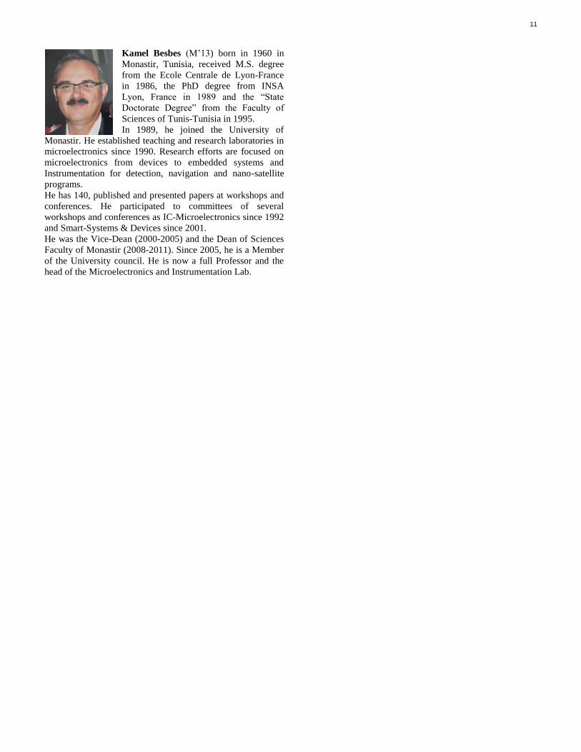
Kamel Besbes (M’13) born in 1960 in
Monastir, Tunisia, received M.S. degree
from the Ecole Centrale de Lyon-France
in 1986, the PhD degree from INSA
Lyon, France in 1989 and the “State
Doctorate Degree” from the Faculty of
Sciences of Tunis-Tunisia in 1995.
In 1989, he joined the University of
Monastir. He established teaching and research laboratories in
microelectronics since 1990. Research efforts are focused on
microelectronics from devices to embedded systems and
Instrumentation for detection, navigation and nano-satellite
programs.
He has 140, published and presented papers at workshops and
conferences. He participated to committees of several
workshops and conferences as IC-Microelectronics since 1992
and Smart-Systems & Devices since 2001.
He was the Vice-Dean (2000-2005) and the Dean of Sciences
Faculty of Monastir (2008-2011). Since 2005, he is a Member
of the University council. He is now a full Professor and the
head of the Microelectronics and Instrumentation Lab.