Embed Size (px)
Citation preview
A Novel Active-Current-Sharing Method for Interleaved Resonant Converters
Yungtaek Jang, Milan M. Jovanović, Juan M. Ruiz, Misha Kumar, and Gang Liu1, 2
Power Electronics Laboratory, Delta Products Corporation, 5101 Davis Drive, Research Triangle Park, NC, USA 1 Electrical Engineering, Fudan University, Shanghai 200433, People’s Republic of China
2 Delta Power Electronics (Shanghai) Co. Ltd, 201209, People’s Republic of China
Abstract— This paper presents a novel active load-current-sharing control of paralleled or interleaved isolated series-resonant converters. In the proposed control method, the output voltage is regulated by variable-frequency control of the converters’ primary switches, while a delay-time control is used to control secondary-side switches provided in place of diode rectifiers to correct load-current imbalance between the converters that is caused by their mismatched components. By independently controlling the turn-off delay time of the secondary switches of each individual converter with respect to the zero-crossing instants of the corresponding resonant-tank current, excellent current balancing can be achieved. The evaluation of the proposed control method was performed on a 1.8-kW prototype that was implemented by two interleaved 900-W series-resonant LLC converters operating from a 240-450-V input-voltage range and providing a 13.8-V output.
I. INTRODUCTION In series-resonant converters (SRCs), including LLC-
resonant converters, the output voltage ripple is determined by the ac-component of the secondary-side rectified resonant current flowing through the output-filter capacitor. As a result, to achieve a low output-voltage ripple in high-current applications, a large output-filter capacitance is required. The output capacitor is typically implemented by paralleling electrolytic capacitors and/or ceramic capacitors. For converter applications that require a relatively long life time such as for example automotive on-board chargers and DC/DC converters, as well as solar inverters and LED drivers, it is not desirable to use electrolytic capacitors because of their relatively short life time [1], [2].
As well known, the output filter capacitance of a converter can be significantly reduced by interleaving, i.e., by paralleling converters and providing a phase shift between their gate-drive signals so that their current ripples at the input and output are greatly reduced. By employing interleaving, resonant converters with a C-type output filter can be designed for high-output-current applications with a reasonable small output filter capacitance. However, interleaving of these variable-frequency controlled resonant converters requires that their switching frequencies are synchronized, i.e., that the converters operate at the same (variable) frequency. However, even with identical input and output voltage and switching frequency, the interleaved resonant converters will not equally share the load current (power) because of inevitable mismatching of their resonant-
tank components. Therefore to achieve acceptable current sharing between the interleaved resonant converters with mismatched components, an additional control means independent of switching-frequency control is required.
So far, a number of approaches for interleaved resonant converters have been introduced, [3]-[7]. Specifically, in [3] and [4], the input of each interleaved converter is connected to a separate dc power source (typically the output of the front-end PFC) and the power source voltages, which are the input voltages of the LLC converters, are controlled to achieve and maintain current balance between the interleaved converters. However, this method cannot be applied in applications where only one dc power source is available. The major drawback of the current-balancing methods based on multiphase resonant-converter approaches introduced in [5] and [6] is that they cannot implement phase shedding to maximize light-load conversion efficiency. The current sharing method in [7] employs additional switches to implement a variable resonant capacitor or inductor that can be controlled to compensate for mismatching of components and equalize the resonant frequencies of the interleaved modules. While the current-sharing performance of this approach has been verified, its major drawback is increased complexity and additional cost.
Recently, a new control method of SRCs that regulates the output voltage with a combination of variable-frequency and delay-time control has been introduced [8]. In this method, the variable-frequency control is used to control the primary switches, while delay-time control is employed to control secondary-side switches provided in place of diode rectifiers. Generally, the major feature of the delay-time control is that it alters the dc-conversion ratio of the SRC by giving it boost characteristics. In this paper, the ability of the delay-time control to modify the converter’s characteristic’s is employed to provide active-current-sharing control of interleaved SRCs that allows phase shedding, does not require any additional power-stage components, and is also applicable to a single DC power source input. In the proposed active current-sharing control, the output voltage is regulated by variable-frequency control of the primary switches of paralleled or interleaved converters, while the delay-time control is used to control secondary-side rectifier switches to correct current imbalance between the two resonant converters. By independently controlling the turn-off delay time of the secondary switches of each individual converter with respect to the zero-crossing instants of the
978-1-4799-6735-3/15/$31.00 ©2015 IEEE 1461
corresponding resonant-tank current, an excellent current balancing can be achieved. The performance evaluation of the proposed active-current-sharing method was done on a 1.8-kW prototype that was implemented by two interleaved 900-W LLC converters operating from the 240-450-V input-voltage range and providing a 13.8-V output.
II. PROPOSED ACTIVE-CURRENT-SHARING METHOD
Figure 1(a) shows two interleaved SRCs with the block diagram of the proposed active-current-sharing control. As shown in Fig. 1(a), the interleaved converters operate with the same switching frequency fS, which is set by the output-voltage controller that includes the output-voltage error amplifier with the compensation circuit and the voltage controlled oscillator (VCO). Frequency fS at VCO is determined by the output-voltage error amplifier based on the voltage difference between scaled sensed output voltage VO(scld) and reference voltage VREF. Interleaving is implemented by phase shifting of the control signals of the corresponding primary switches of the two converters by 900, i.e., by one-quarter of the switching period TS/4, as shown in Figure 1(b).
In the implementation example in Fig. 1(a), the output currents of the paralleled converters are not sensed directly. Instead, the output currents are obtained indirectly from sensed secondary currents iS1 and iS2. In Fig. 1(a), secondary currents iS1 and iS2 are rectified and filtered to provide currents <|iS1|> and <|iS2|> which are proportional to corresponding output currents. The differences between currents <|iS1|> and <|iS2|> are processed by the respective current-sharing error amplifier that sets the delay time of the corresponding secondary switches relative to the secondary current zero crossings. Since a typical current mismatch between parallel converters is relatively small, the delay times required for current balancing are also relatively short.
As shown in Fig. 1(b), switches in the same leg of the primary sides of the converters operate in a complementary fashion with a small dead time between their commutations to achieve ZVS. The delay-time control is implemented by delaying the turn-off of switches SS11 and SS21 of CONVERTER 1 with respect to the corresponding zero crossings of secondary-side resonant current iS1 so that both switches SS11 and SS21 are turned on during delay-time interval [T0-T1] shorting the secondary of transformer TR1. Similarly, the turn-off of switches SS12 and SS22 of CONVERTER 2 is delayed with respect to the corresponding zero crossings of secondary-side resonant current iS2 so that both switches SS12 and SS22 are turned on during delay-time interval [T2-T3]. Because the secondary of the transformers is shorted during delay-time intervals [T0-T1] and [T2-T3], the voltage across resonant tank LR-CR during delay-time intervals is VIN instead of VIN –nVO which is the case with no delay-time control. Therefore, with the delay-time control, a higher voltage is applied across the resonant tank and, consequently, a higher amount of energy is stored in resonant inductor LR. Therefore, for the same input voltage and switching frequency, secondary-side delay-
(a)
(b) Fig. 1. Interleaved series-resonant converters with active current-sharing
control implemented with secondary-switch delay-time control: (a) block diagram; (b) switch control and resonant inductor waveforms.
VINVO
+
-S S11
TR1LOAD
i S1
SS21
D D1121
LR1
VoltageControlledOscillator
(VCO)
TR2
iS2
D22
VEA
LR2
CURRENT-SHAREERROR AMPLIFIERw/ COMPENSATION
VCS1
DRIVER
fS
fS
I O
D12
SS12SS22
SP11
SP21
CR11
CR21
CO
DELAY-TIMECONTROL
DRIVER
ZCD
output voltagesensing &
scaling
CURRENT-SHAREERROR AMPLIFIERw/ COMPENSATION
VCS2DELAY-TIMECONTROL
DRIVER
OUTPUT-VOLTAGE ERROR AMPLIFIERw/ COMPENSATION
SP12
SP22
CR21
CR22
DRIVER
CONVERTER 2
CONVERTER 1
<|i |>S1
<|i |>S2
ZCD
VREF
VO(scld)
RECTIFIERAND FILTER
<|i |>S2
<|i |>S1
RECTIFIERAND FILTER
90 DEGREEPHASE SHIFT
i P1
i P2
N2N1N1
N2n=
N2N1
OFF ON
t
t
ONOFF
OFFON
t
T0 T4T1 T5
Ts
t
ON OFF
t
SS11
SS21
SP11
SP21
i S1
T6
t
t
t
t
SS12
SS22
SP12
SP22 OFF ON
ON OFF
OFFON
Ts/4
ONOFF
i S2 i S1
i S2
Delay Time 1
Delay Time 2
T2 T3
TD1
TD2
1462
time control provides a higher output voltage compared to the conventional frequency control.
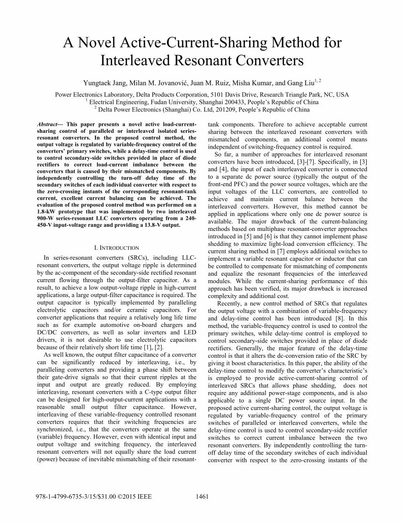
Figure 2 shows the calculated dc conversion ratio M= nVO/VIN of the SRC with delay-time control as a function of normalized switching frequency fN=fS/fO and with Q-factor ⁄ / and normalized delay time TD_N=TD/TS as parameters. It should be noted that control characteristics with delay time TD=0 are those of the conventional SRC. Derivations of the dc-conversion ratio characteristics shown in Fig. 2 are given in [8].
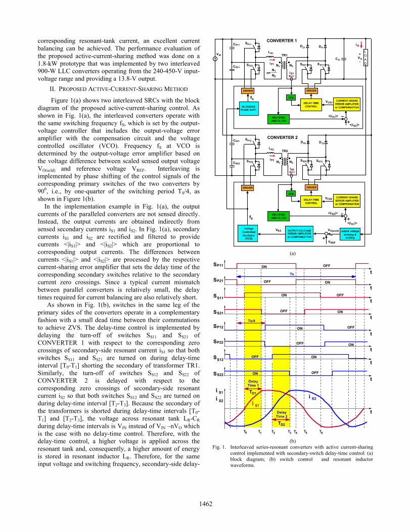
To illustrate how the proposed delay-time control achieves active balancing of the output currents of two interleaved converters, Fig. 3 shows the dc characteristics of two converters with mismatched components. The characteristics of the reference converter, CONVERTER 1, without delay-time control (TD=0) for Q=1 is shown with the solid red line. The corresponding characteristics of the
mismatched converter, CONVERTER 2, is shown with the solid blue line. Because of the mismatching, the converters have different resonant frequencies, i.e., the resonant frequency of CONVERTER 1 is fO while that of CONVERTER 2 is assumed to be 1.1×fO. Because the characteristics are shifted from each other, to regulate the same output voltage they require different frequencies, as illustrated in Fig. 3 by operating points A and B on the constant-gain line (M=0.92). As also can be seen in Fig. 3, for the same input voltage and switching frequency the output voltage of CONVERTER 2 is higher than that of CONVERTER 1, as illustrated with operating points B and C on the constant-frequency line (fN=1.24) in Fig. 3. Therefore, if the two interleaved converters were driven by the same switching frequency, CONVERTER 2 would process the entire output power, while CONVERTER 1 would be practically off. However, because of the boost characteristics of the delay-time control, the output voltage (gain) of CONVERTER 1 can be increased, as shown in Fig. 3 with dashed red lines that correspond to normalized delay time TD_N=TD/TS=0.05 and TD_N=0.1. As can be seen from Fig. 3, for D=0.05 the gain of CONVERTER 1 at normalized frequency fN=1.24 is increased to the level of CONVERTER 2 gain, i.e., both converter can control the specified output voltage at the same frequency enabling interleaved operation with current (power) sharing.
The proposed control can be implemented by either
(a)
(b) Fig. 2. Calculated dc-voltage conversion ratio M of SRC with the delay-
time control for Q-factor: (a) Q=1; (b) Q=0.5. It should be notedthat control characteristics with TD_N=0 is equal to that ofconventional SRC.
1 1.1 1.2 1.3 1.4 1.50.6
0.7
0.8
0.9
1
1.1
1.2
1.3
=0
1.16 1.41
M=0.9
Q = = 1
0.1
0.05
= 0.125
0.025
0.075BOOST MODE OPERATION
M =
fN =
1 1.2 1.4 1.6 1.8 20.6
0.7
0.8
0.9
1
1.1
1.2
1.3
0.1
0.05
0.025
0.075
M=0.9
BOOST MODE OPERATION
=0
Q = = 0.5= 0.125
M =
fN =
1.29 1.88
Fig. 3. Calculated dc-voltage conversion ratio M of two mismatched converters for Q=1 without delay-time control (solid lines) and with delay-time control for TD_N=0.05 and TD_N=0.1 (dashed lines). Without delay-time control, two converters cannot regulate output voltage at M=0.92 with the same switching frequency fN=1.24. By actively increasing delay-time of CONVERTER 1, two converters can eventually operate at the same frequency and with balanced output currents.
=0.05
=0
=0.1
1.13 1.24
M=0.92
fO1 = fO
CONVERTER 1
Q=1
CONVERTER 2
A
C
B=0
M =
fN =
Q =
fO2 = 1.1 × fO
Q=1
Q=1
Q=1
0.9
1
0.7
0.8
1.1
1.2
1.2 1.31.11 1.4
1463
analog, digital technique, or their combination. A microcontroller- or DSP-based implementation is preferred, because of excellent performance of today’s DSPs.
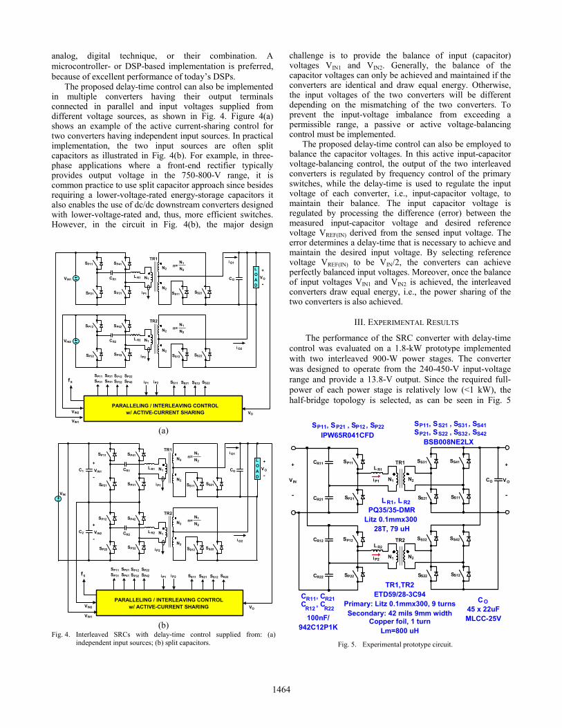
The proposed delay-time control can also be implemented in multiple converters having their output terminals connected in parallel and input voltages supplied from different voltage sources, as shown in Fig. 4. Figure 4(a) shows an example of the active current-sharing control for two converters having independent input sources. In practical implementation, the two input sources are often split capacitors as illustrated in Fig. 4(b). For example, in three-phase applications where a front-end rectifier typically provides output voltage in the 750-800-V range, it is common practice to use split capacitor approach since besides requiring a lower-voltage-rated energy-storage capacitors it also enables the use of dc/dc downstream converters designed with lower-voltage-rated and, thus, more efficient switches. However, in the circuit in Fig. 4(b), the major design
challenge is to provide the balance of input (capacitor) voltages VIN1 and VIN2. Generally, the balance of the capacitor voltages can only be achieved and maintained if the converters are identical and draw equal energy. Otherwise, the input voltages of the two converters will be different depending on the mismatching of the two converters. To prevent the input-voltage imbalance from exceeding a permissible range, a passive or active voltage-balancing control must be implemented.
The proposed delay-time control can also be employed to balance the capacitor voltages. In this active input-capacitor voltage-balancing control, the output of the two interleaved converters is regulated by frequency control of the primary switches, while the delay-time is used to regulate the input voltage of each converter, i.e., input-capacitor voltage, to maintain their balance. The input capacitor voltage is regulated by processing the difference (error) between the measured input-capacitor voltage and desired reference voltage VREF(IN) derived from the sensed input voltage. The error determines a delay-time that is necessary to achieve and maintain the desired input voltage. By selecting reference voltage VREF(IN) to be VIN/2, the converters can achieve perfectly balanced input voltages. Moreover, once the balance of input voltages VIN1 and VIN2 is achieved, the interleaved converters draw equal energy, i.e., the power sharing of the two converters is also achieved.
III. EXPERIMENTAL RESULTS
The performance of the SRC converter with delay-time control was evaluated on a 1.8-kW prototype implemented with two interleaved 900-W power stages. The converter was designed to operate from the 240-450-V input-voltage range and provide a 13.8-V output. Since the required full-power of each power stage is relatively low (<1 kW), the half-bridge topology is selected, as can be seen in Fig. 5
(a)
(b) Fig. 4. Interleaved SRCs with delay-time control supplied from: (a)
independent input sources; (b) split capacitors.
SP21
VIN1 VO
+
-
LOAD
SP11
L R1 CO
SS21SS11
TR1
N1
N2
N2
N1
N2n=SP41
SP31
CR1
SP22
VIN2
SP12
L R2
SS22SS12
TR2
N1
N2
N2
N1
N2n=SP42
SP32
CR2
PARALLELING / INTERLEAVING CONTROLw/ ACTIVE-CURRENT SHARING VO
SP41SP31
VIN2
SS12SS21SS11 SS22
VIN1
SP42SP32
i O1
i O2
iP1
iP1 iP2
iP2
SP21SP11 SP22SP12fS
SP21
VIN1VO
+
-
LOAD
SP11
LR1 CO
SS21SS11
TR1
N1
N2
N2
N1
N2n=SP41
SP31
CR1
SP22
SP12
LR2
SS22SS12
TR2
N1
N2
N2
N1
N2n=SP42
SP32
CR2
PARALLELING / INTERLEAVING CONTROLw/ ACTIVE-CURRENT SHARING VO
SP41SP31
VIN2
SS12SS21SS11 SS22
VIN1
SP42SP32
i O1
i O2
iP1
iP1 iP2
iP2
SP21SP11 SP22SP12fS
VIN
C1
+
-
VIN2C2
+
-
Fig. 5. Experimental prototype circuit.
TR1,TR2ETD59/28-3C94
Primary: Litz 0.1mmx300, 9 turnsSecondary: 42 mils 9mm width
Copper foil, 1 turnLm=800 uH
IPW65R041CFD
TR1
VO
+
-
CO
SS41
SS11
N2
SS31
SS21
CR11
CR21
SP11
SP21
L R1
N1VIN
+
-
TR2 SS42
SS12
N2
SS32
SS22
CR12
CR22
SP12
SP22
L R2
N1
S , S , S , SP11 P21 P12 P22
L , LPQ35/35-DMR
Litz 0.1mmx300 28T, 79 uH
R1 R2
BSB008NE2LXS , S , S , SP21 S22 S32 S42
S , S , S , SP11 S21 S31 S41
CO45 x 22uFMLCC-25V
iP1
iP2
C , CR11 R21
R12 R22
100nF/942C12P1K
C , C
1464
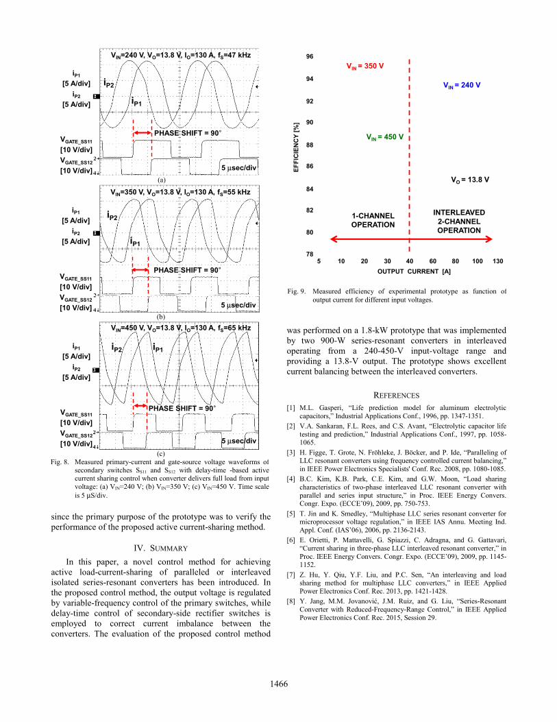
which shows the circuit diagram of the experimental circuit. The list of semiconductor and passive components used in the experimental prototype circuit are given in Table I and Table II, respectively. Figure 6 shows a photo of the prototype.
It should be noted that because the secondary circuit layout is designed to cancel the output current ripples of the interleaved converters, the output rectifier switches of the two power stages and output capacitors (forty five 22-μF multi-layer ceramic capacitors in parallel) are tightly interconnected. As a result, measuring the output current of the individual power stage is not physically possible in this prototype since no single trace is available that carries the
total current of the individual converters. However, since the magnetizing current of the proposed converter is much smaller than the resonant current due to a relative large magnetizing inductance, the measured primary current waveform of each power stage is proportional to its secondary current waveform whose rectified average represents the output current.
Figure 7 shows measured primary-current and gate-voltage waveforms of secondary switches SS11 and SS12 when the converter operates without current sharing control and delivers 40-A load from the 240-V input. As seen in Fig. 7, because of resonant-component mismatching, primary currents iP1 and iP2 are significantly imbalanced, i.e., the interleaved power stages do not share the load current (power) well.
Figures 8(a), (b), and (c) show the measured waveforms of primary currents iP1 and iP2 along with the gate-drive waveforms of secondary switches SS11 and SS12 when the circuit operates with proposed current sharing control and delivers full power from the 240-V, 350-V, and 450-V input, respectively. The measured waveforms show a very good current balance of the two interleaved converters. To avoid control loop interactions, the bandwidth of the delay-time control loop is set to approximately 100 Hz which is about ten times lower than that of the variable-frequency output-voltage regulation loop.
Finally, Fig. 9 shows measured efficiency of the prototype as a function of the load current for different input voltages. The two power stages operate in interleaved mode from full load down to 30 % of the full load. When the output power decreases below 30% of the full load, i.e., at approximately 40 A, one power stage is turned off to improve the light load efficiency. The converter exhibits the highest full-load efficiency of 94.8% for the nominal voltage of 350 V. The peak efficiency occurs of 95.4% occurs at the 40% of the full load and nominal input voltage. It should be noted that the full-load efficiency of the prototype could have been increased for 1.5-2.5% by further optimization. However, this additional optimization has not been done
TABLE I Semiconductor component list
TABLE II Passive component list
Name Parameters
Primary Switches:SP11 , SP21, SP12, SP22
IPW65R041CFD (TO-247)650 V, 0.41 mΩ
Secondary SR Switches:SS11, SS21, SS22, SS12, D11, D21, D22, D12
BSB008NE2LX (CanPAK)25 V, 0.08 mΩ
DSP Controller TMS320F28027 (TI)
Driver SI8235 (Silicon Lab)
Name Parameters
CR11, CR21, CR21, CR22 100nF-942C12P1K – CDE (9.2 ARMS)
CO 22μF-MLCC-25 V, 45 in parallel
LR1, LR2 79uH (PQ35/35 — DMR)
LR Winding 0.1mm×300 strands 28Ts
TR1, TR2 : Lm 800uHTR1, TR2 :Turn Ratio 9:1 (ETD59/28 — 3C94)
TR1, TR2 : Primary Winding 0.1mm×300 strands 9Ts
TR1, TR2 : Secondary Winding 42 mils (1.067 mm), 9mm Width, copper foil 1Turn
Resonant Frequency 40kHz
(c)
Fig. 7. Measured primary-current and gate-source voltage waveforms of secondary switches SS11 and SS12 when converter operates without current sharing control and delivers 40-A load from 240-V input. Time scale is 5 μS/div.
VIN=240 V, VO=13.8 V, IO=40 A, fS=70 kHz
iP1
[2 A/div]iP2
[2 A/div]
VGATE_SS11
[5 V/div]VGATE_SS12
[5 V/div]
5 μsec/diviP2 iP1
Fig. 6. Experimental prototype circuit.
1465
since the primary purpose of the prototype was to verify the performance of the proposed active current-sharing method.
IV. SUMMARY In this paper, a novel control method for achieving
active load-current-sharing of paralleled or interleaved isolated series-resonant converters has been introduced. In the proposed control method, the output voltage is regulated by variable-frequency control of the primary switches, while delay-time control of secondary-side rectifier switches is employed to correct current imbalance between the converters. The evaluation of the proposed control method
was performed on a 1.8-kW prototype that was implemented by two 900-W series-resonant converters in interleaved operating from a 240-450-V input-voltage range and providing a 13.8-V output. The prototype shows excellent current balancing between the interleaved converters.
REFERENCES
[1] M.L. Gasperi, “Life prediction model for aluminum electrolytic capacitors,” Industrial Applications Conf., 1996, pp. 1347-1351.
[2] V.A. Sankaran, F.L. Rees, and C.S. Avant, “Electrolytic capacitor life testing and prediction,” Industrial Applications Conf., 1997, pp. 1058-1065.
[3] H. Figge, T. Grote, N. Fröhleke, J. Böcker, and P. Ide, “Paralleling of LLC resonant converters using frequency controlled current balancing,” in IEEE Power Electronics Specialists' Conf. Rec. 2008, pp. 1080-1085.
[4] B.C. Kim, K.B. Park, C.E. Kim, and G.W. Moon, “Load sharing characteristics of two-phase interleaved LLC resonant converter with parallel and series input structure,” in Proc. IEEE Energy Convers. Congr. Expo. (ECCE’09), 2009, pp. 750-753.
[5] T. Jin and K. Smedley, “Multiphase LLC series resonant converter for microprocessor voltage regulation,” in IEEE IAS Annu. Meeting Ind. Appl. Conf. (IAS’06), 2006, pp. 2136-2143.
[6] E. Orietti, P. Mattavelli, G. Spiazzi, C. Adragna, and G. Gattavari, “Current sharing in three-phase LLC interleaved resonant converter,” in Proc. IEEE Energy Convers. Congr. Expo. (ECCE’09), 2009, pp. 1145-1152.
[7] Z. Hu, Y. Qiu, Y.F. Liu, and P.C. Sen, “An interleaving and load sharing method for multiphase LLC converters,” in IEEE Applied Power Electronics Conf. Rec. 2013, pp. 1421-1428.
[8] Y. Jang, M.M. Jovanović, J.M. Ruiz, and G. Liu, “Series-Resonant Converter with Reduced-Frequency-Range Control,” in IEEE Applied Power Electronics Conf. Rec. 2015, Session 29.
(a)
(b)
(c)
Fig. 8. Measured primary-current and gate-source voltage waveforms ofsecondary switches SS11 and SS12 with delay-time -based active current sharing control when converter delivers full load from inputvoltage: (a) VIN=240 V; (b) VIN=350 V; (c) VIN=450 V. Time scale is 5 μS/div.
VIN=240 V, VO=13.8 V, IO=130 A, fS=47 kHz
iP1
[5 A/div]iP2
[5 A/div]
VGATE_SS11
[10 V/div]VGATE_SS12
[10 V/div] 5 μsec/div
PHASE SHIFT = 90°
iP2
iP1
VIN=350 V, VO=13.8 V, IO=130 A, fS=55 kHz
iP1
[5 A/div]iP2
[5 A/div]
VGATE_SS11
[10 V/div]VGATE_SS12
[10 V/div] 5 μsec/div
PHASE SHIFT = 90°
iP2
iP1
VIN=450 V, VO=13.8 V, IO=130 A, fS=65 kHz
iP1
[5 A/div]iP2
[5 A/div]
VGATE_SS11
[10 V/div]VGATE_SS12
[10 V/div] 5 μsec/div
PHASE SHIFT = 90°
iP2 iP1
Fig. 9. Measured efficiency of experimental prototype as function of
output current for different input voltages.
OUTPUT CURRENT [A]
EFFI
CIE
NC
Y [%
]
VO = 13.8 V
INTERLEAVED 2-CHANNEL OPERATION
1-CHANNEL OPERATION
VIN = 350 V
VIN = 240 V
VIN = 450 V
96
94
92
90
88
86
84
82
80
785 10 20 30 40 60 80 100 130
1466


![Simulation of a Novel Phase-Shift Operated Interleaved ... · A novel snubberless CFHB front-end isolated dc/dc converter-based inverter for PV applications is introduced in [12]](https://img.pdfslide.us/doc/110x75/5e689d1944caa440c84a49e7/simulation-of-a-novel-phase-shift-operated-interleaved-a-novel-snubberless-cfhb.jpg)