Embed Size (px)
Citation preview

A NEW SIMPLIFIED SVPWM ALGORITHM BASED ON MODIFIEDCARRIER SIGNAL
Raymundo Cordero García∗
[email protected]ão Onofre Pereira Pinto∗
∗UFMS – Federal University of Mato Grosso do Sul,Department of Electric Engineering,
CEP 79074-460 – Campo Grande, Mato Grosso do Sul, Brazil.
RESUMO
Um novo algoritmo SVPWM simplificado baseado em si-nal portador modificadaEste artigo apresenta um algoritmo simplificado da modu-lação por largura de pulso por vetores espaciais (SVPWM)para um inversor trifásico de dois níveis, o qual pode ope-rar em submodulação e sobremodulação. Em outras simpli-ficações achadas na literatura, as tensões de referência sãomodificadas e comparadas com um portador triangular paraestimar os estados de comutação do inversor. Não obstante,este artigo propõe a modificação do portador, em lugar dasreferências. Este procedimento reduz o número de opera-ções matemáticas e aumenta a velocidade de execução doalgoritmo SVPWM em DSPs ou FPGAs. As ondas de re-ferência são senoidais, ainda no modo de sobremodulação.Resultados de simulação e experimentais demonstram que asimplificação proposta produz o mesmo padrão de chavea-mento que o SVPWM convencional, é mais simples e rápidaque outras simplificações.
PALAVRAS-CHAVE: Inversor trifásico de dois níveis, modu-lação por largura de pulso por vetores espaciais, sinal porta-dor triangular, submodulação, sobremodulação.
ABSTRACT
This paper presents a simplified algorithm of space vectorpulse width modulation (SVPWM) for a two-level three-
Artigo submetido em 23/06/2010 (Id.: 01163)Revisado em 21/09/2010, 24/03/2011Aceito sob recomendação do Editor Associado Prof. José Antenor Pomilio
phase inverter, which can operate in undermodulation andovermodulation modes. In other simplifications founded inliterature, the reference voltages are modified and comparedwith a triangular carrier to estimate the switching states ofthe inverter. However, this paper proposes the modificationof the carrier signal instead of the references. This proce-dure reduces the number of mathematical operations and in-creases the execution speed of SVPWM algorithm in DSPsor FPGAs. The reference voltages are sinusoidal, even forovermodulation mode. Simulation and experimental resultsproves that the proposed simplification produces the sameswitching patterns than conventional SVPWM, is simplerand is faster than other simplifications.
KEYWORDS: Two-level three-phase inverter, space vectorpulse width modulation, triangular carrier signal, undermod-ulation, overmodulation.
1 INTRODUCTION
Space Vector PWM (SVPWM) is widely used in variable fre-quency drive applications, by its superior harmonic quality,less switching losses and extended linear range of operation(Holtz, 1994; Van der Broeck et al., 1988; Yu et al., 2008).However, its conventional implementation requires a highnumber of mathematical operations, reducing the maximumspeed that SVPWM can be executed in DSPs or FPGAs.
Different researches were made to simplify SVPWM: Thereal and imaginary components of space vectors are usedto calculate the switching times without using trigonomet-ric functions (Shu et al., 2007; Yu, 1999; Zhai and Li, 2008).
Revista Controle & Automação/Vol.22 no.5/Setembro e Outubro 2011 545

In Lamich et al. (2002), Zhang et al. (2009), the switch-ing times are defined in terms of the phase references in-stead of using space vectors. According to Blasko (1997),Holmes (1996), SVPWM is equivalent to sinusoidal modu-lation when a zero-sequence component is added to the ref-erence signals. In Pinheiro et al. (2005) SVPWM is easilyimplemented when the neutral points of the inverter and theload are connected, establishing the concepts of decomposi-tion matrices.
On the other hand, the SVPWM algorithm must operate inovermodulation mode to generate as high AC voltages aspossible for a given DC energy source. Different techniquesin literature (Bakhshai et al., 2000; Filho et al., 2004; Pintoet al., 2000; Yang et al., 2009) modify the references sig-nals, adapting the formulas for undermodulation mode toovermodulation mode. Those values are compared with atriangular carrier to establish the switching sequence.
In this paper, the number of mathematical operations to im-plement SVPWM algorithm, even for overmodulation mode,is reduced by the modification of the carrier signal instead ofthe references voltages.
The modified carrier depends on the zero-sequence compo-nent described in Blasko (1997) and the modulation index.On the other hand, the reference voltages are sinusoidal, evenfor overmodulation mode. This fact simplifies the implemen-tation of SVPWM.
The proposed technique based on modified carrier is com-pared with conventional SVPWM, Hybrid PWM and the al-gorithm described in Filho et.al. (2004). Simulation and ex-perimental results demonstrate that the proposed simplifica-tion based on modified carrier generates the same switchingpatterns than conventional SVPWM, requires a less numberof arithmetic operations and its execution is faster than othersimplifications.
2 SPACE VECTOR PWM
2.1 Two-Level Three-Phase Inverter
The structure of a two-level three-phase voltage source in-verter is shown in Figure 1. It is composed by six powertransistors (MOSFTET, IGBT, GTO) Qa, Qan, Qb, Qbn, Qc
and Qcn, which are controlled by the digital signals sa, san,sb, sbn, sc and scn, respectively. To avoid short circuit in theenergy source and indeterminate output voltages, the switch-ing states of the upper transistors (Qa, Qb or Qc) and thelower transistor (Qan, Qbn or Qcn respectively) in the sameleg are opposite.
Pole voltages vaN , vbN and vcN are the terminal voltages ofeach leg respect to the neutral point N (reference point of theDC supply). These voltages depend of the switching statesof the transistors (Yu, 1999), according to equation (1) :
vpN =
{
0, 5vdc; ifsp = 1(switchedon)−0, 5vdc; ifsp = 0(switchedoff)
(1)
Where p denotes the phase of the inverter (p = a, b, c). Equa-tion 1 indicates that each output of the inverter has two possi-ble values. Therefore, there are 23 = 8 switching states, withtheir respective output voltages.
In general, the phase voltages (vaO, vbO, vcO) of a balancedstar-connected load fed by a three phase voltage source, as atwo-level inverter, depend on the pole voltages (Bose, 2002):
vaO
vbO
vcO
=1
3
2 −1 −1−1 2 −1−1 −1 2
vaN
vbN
vcN
(2)
2.2 Space Vector Representation
A set of balanced three-phase voltages [vavbvc]T can be rep-
resented through a space vector, a complex number with areal (vα) and an imaginary (vβ) components defined in thecomplex plane, according to equation (3) (Rashid, 2001):
V =
[
vα
vβ
]
=2
3
[
2va − (vb + vc)√3 (vb − vc)
]
(3)
Table 1 shows the space vectors that represents the eightswitching states of the two-level inverter. Six non-zero vec-tors (from V1 to V6) divide the complex plane in six sectorsof a hexagon, as illustrated in Figure 2. On the other hand,two zero vectors (V0 and V7) are located at the center of thehexagon.
Table 1: Output Voltages of the Two-Level Inverter
Vector sa sb sc vα vβ
v0 0 0 0 0 0v1 1 0 0 − 2
3vdc 0v2 1 1 0 1
3vdc13vdc
v3 0 1 0 − 13vdc
1√3vdc
v4 0 1 1 − 23vdc 0
v5 0 0 1 − 13vdc − 1√
3vdc
v6 1 0 1 13vdc − 1√
3vdc
v7 1 1 1 0 0
546 Revista Controle & Automação/Vol.22 no.5/Setembro e Outubro 2011

The desired pole voltages [vravrbvrc]T are represented by
the vector Vr, using equation (3) . According to equation(2) , if the pole references belong to a balanced system, thenthey are equal to the load phase references. This vector isapproximated with a combination of the space vectors V0 toV7, during the modulation period tm, according to equations(4) and (5) :
Vrtm = Vxtx + Vyty (4)
tz = tm − (tx + ty) (5)
Where tx, ty and tz are the switching times that Vx, Vy andthe zero vector Vz are used, respectively. If Vr is located insector s: Vx = Vs and Vy = Vs+1 (except in sector 6, whereVy = V1).
Conventionally, the switching times are calculated usingtrigonometric functions, according to equations (6) and (7)(Bose, 2002):
tx =√
3tm‖Vr‖vdc
sin(π
3− g
)
(6)
Figure 1: Two-level three-phase inverter.
Figure 2: Zero and non-zero vectors of the inverter.
ty =√
3tm‖Vr‖vdc
sin (g) (7)
Where || Vr || is the magnitude of the reference vector, andg is the angle between Vr and Vx, as shown in Figure 2.Trigonometric functions demand many mathematical opera-tions in DSPs or FPGAs. In order to resolve this problem,the switching times can also be calculated using the real andimaginary components of the space vectors. Applying sub-matrix algebra (Cheng, 1999) to equation (4) :
Vrtm =[
Vx Vy
] [
tx ty]T
(8)
Figure 2 proves that the vectors Vx and Vy are not collinear.Therefore, the matrix [Vx Vy] is invertible (Cheng, 1999).Considering Vr = [vrα vrβ ]T , Vx= [vxαvxβ ]T and Vy =[vyαvyβ ]T , the switching times can be calculated as follows:
[
txty
]
=[
Vx Vy
]−1Vrtm
[
txty
]
=
[
vxα vyα
vxβ vyβ
]−1 [
vrα
vrβ
]
tm
(9)
Table 2 shows the values of tx and ty for each sector, ac-cording to equation (8) . The value of tz is obtained us-ing equation (5) . After those operations, the sequence ofthe switching states of the upper transistors must be defined.This arrangement can be done in different ways (Hariramand Marimuthu, 2005). This paper considers the software-determined switching pattern described in Yu (1999) and il-lustrated in Figure 3.
Table 2: Switching Times in Function of vrα and vrβ
Sector tx ty1 tm
2vdc
(
3vrα −√
3vrβ
)
tm
vdc
(√3vrβ
)
2 tm
2vdc
(
3vrα +√
3vrβ
)
tm
2vdc
(
−3vrα +√
3vrβ
)
3 tm
vdc
(√3vrβ
)
tm
2vdc
(
−3vrα −√
3vrβ
)
4 tm
2vdc
(
−3vrα +√
3vrβ
)
tm
vdc
(
−√
3vrβ
)
5 tm
2vdc
(
−3vrα −√
3vrβ
)
tm
2vdc
(
3vrα −√
3vrβ
)
6 tm
vdc
(
−√
3vrβ
)
tm
2vdc
(
3vrα +√
3vrβ
)
2.3 Operation Modes of SVPWM
The modulation index m is defined as follows (Holtz, 1994):
m =‖Vr‖(
2πvdc
) (10)
Where 2vdc/π is the fundamental peak value of the squarevoltage wave. The modulation index varies from 0 to 1,defining three operation modes (Bose, 2002):
Revista Controle & Automação/Vol.22 no.5/Setembro e Outubro 2011 547

• Undermodulation mode (0 ≤ m < 0,907): The refer-ence vector always reminds within the hexagon, whilethe reference voltages are perfectly sinusoidal.
• Overmodulation mode 1 (0,907 ≤ m < 0,952): Thereference vector crosses the hexagon at two points ineach sector. When SVPWM operates in overmodula-tion mode, there is a loss in the magnitude of the funda-mental voltage. To compensate this effect, the referencevoltages must be modified. In overmodulation mode 1,those references are composed by linear and sinusoidalsegments.
• Overmodulation mode 2 (0,952 ≤ m ≤ 1): The refer-ence vector increases even further compared with over-modulation mode 1. The reference voltages are com-posed only by linear segments.
Figures 4, 5 and 6 show the operation region in sector 1and the reference voltages for the three operation modes ofSVPWM.
Figure 3: Software-determined switching sequence.
Figure 4: Operation region in sector 1 and reference voltagefor undermodulation mode.
2.4 Turn-on Times
In order to simplify SVPWM algorithm, the turn-on timesta−on, tb−on and tc−on are defined in Filho et al. (2004) toestimate the state of the upper transistors, to avoid working
Figure 5: Operation region in sector 1 and reference voltagefor overmodulation mode 1.
Figure 6: Operation region in sector 1 and reference voltagefor overmodulation mode 2.
with the switching times tx, ty and tz . The formulas of theturn-on times for the sector s (from 1 to 6) are presented inequations (11) , (12) and (13) :
ta−on =
tm
2
[
1 + 3fc
2vdc
(
−vrα − vrβ√3
)]
; s = 1, 4
tm
2
[
1 + 3fc
2vdc(−2vrα)
]
; s = 2, 5
tm
2
[
1 + 3fc
2vdc
(
−vrα +vrβ√
3
)]
; s = 3, 6
(11)
tb−on =
tm
2
[
1 + 3fc
2vdc
(
vrα −√
3vrβ
)
]
; s = 1, 4
tm
2
[
1 + 3fc
2vdc
(
−2vrβ√
3
)]
; s = 2, 5
tm
2
[
1 + 3fc
2vdc
(
vrα − vrβ√3
)]
; s = 3, 6
(12)
tc−on =
tm
2
[
1 + 3fc
2vdc
(
vrα +vrβ√
3
)]
; s = 1, 4
tm
2
[
1 + 3fc
2vdc
(
2vrβ√
3
)]
; s = 2, 5
tm
2
[
1 + 3fc
2vdc
(
vrα +√
3vrβ
)
]
; s = 3, 6
(13)
The factor fc compensates the attenuation of the fundamen-tal voltage in overmodulation mode. This compensation fac-tor can be implemented in a look-up table, and depends onthe modulation index: fc is unity in undermodulation mode,and it tends to infinite in overmodulation mode (Filho et al.,2004).
548 Revista Controle & Automação/Vol.22 no.5/Setembro e Outubro 2011

The advantages of working with turn-on times is that theswitching states can be easily determined by a simple com-parison with a triangular carrier c(t), as illustrated in Figure7 (Pinto et al., 2000). However, the formulas of the turn-ontimes require many mathematical operations for each sectorand phase. This problem is solved using the concept of mod-ified carrier signal, which is explained in sequence below.
3 PROPOSED ALGORITHM
3.1 Simplified Formulas about Turn-onTimes
In Zhang et al. (2009), the switching times tx and ty areexpressed in terms of the reference voltages. In this paper,the same strategy is used, but to express the turn-on timesta−on, tb−on and tc−on. For example, according to equation(11) , the turn-on time for the phase a in sector 1 is:
ta−on =tm2
[
1 +3fc
2vdc
(
−vrα − vrβ√3
)]
; s = 1, 4 (14)
On the other hand, based on equation (3) :
−vrα − vrβ√3
= − 2vra−(vrb+vrc)3 − 1√
3
(vrb−vrc)√3
−vrα − vrβ√3
= −2(vra−vrc)3
(15)
As the sum of the three reference voltages is zero in a bal-anced three-phase system (vra + vrb + vrc = 0):
−vrc = vra + vrb (16)
Figure 7: Comparison between tp−on and the carrier c(t).
Replacing equations (15) and (16) in equation (14) :
ta−on = tm
2
[
1 − fc(vra−vrc)
vdc
]
; s = 1, 4
ta−on = tm
2
[
1 − fc(2vra+vrb)
vdc
]
; s = 1, 4(17)
Using the similar procedure to obtain equation (17) , the turn-on times are defined in function of the reference voltages:
ta−on =
tm
2
[
1 − fc(2vra+vrb)
vdc
]
; s = 1, 4
tm
2
[
1 − fc(2vra+vra)
vdc
]
; s = 2, 5
tm
2
[
1 − fc(2vra+vrc)
vdc
]
; s = 3, 6
(18)
tb−on =
tm
2
[
1 − fc(2vrb+vrb)
vdc
]
; s = 1, 4
tm
2
[
1 − fc(2vrb+vra)
vdc
]
; s = 2, 5
tm
2
[
1 − fc(2vrb+vrc)
vdc
]
; s = 3, 6
(19)
tc−on =
tm
2
[
1 − fc(2vrc+vrb)
vdc
]
; s = 1, 4
tm
2
[
1 − fc(2vrc+vra)
vdc
]
; s = 2, 5
tm
2
[
1 − fc(2vrc+vrc)
vdc
]
; s = 3, 6
(20)
Equations (18) , (19) and (20) have the following structure:
tp−on =tm2
[
1 − fc
(2vrp + vzs)
vdc
]
(21)
Where vrp is the reference voltage in phase p, while vzs isbased on the zero-sequence component described in Blasko(1997), and depends on the sector s where the reference vec-tor is located:
vzs =
vrb; s = 1, 4vra; s = 2, 5vrc; s = 3, 6
(22)
3.2 Modified Carrier Signal
Equation (21) can be expressed as follows:
tp−on =tm2
− fc
(
tm2vdc
)
(2vrp + vzs) (23)
If the terms tm/2 and tm/(2vdc) are considered as constants,then six multiplications are needed to calculate the turn-ontimes using equation (23) , without considering the estima-tion of the compensation factor fc.
However, it is possible to reduce even more the number ofmathematical operations using the concept of modified car-rier proposed in this paper.
Revista Controle & Automação/Vol.22 no.5/Setembro e Outubro 2011 549

Figure 7 indicates that the upper transistor Qp is switched on(sp = 1) when the carrier c(t) is greater than the turn-on time:
c (t) ≥ tp−on (24)
From equations (23) and (24) :
c (t) ≥ tm
2
[
1 − fc(2vrp+vzs)
vdc
]
2c(t)tm
≥[
1 − fc(2vrp+vzs)
vdc
]
2vrp + vzs ≥ vdc
fc
[
1 − 2c(t)tm
]
2vrp ≥ vdc
fc
[
1 − 2c(t)tm
]
− vzs
(25)
Dividing equation (25) by the amplitude of the reference vec-tor ||Vr||:
2vrp
‖Vr‖ ≥ vdc
‖Vr‖fc
[
1 − 2c(t)tm
]
− vzs
‖Vr‖2vrp
‖Vr‖ ≥(
2vdc
‖Vr‖π
) (
π2fc
) [
1 − 2c(t)tm
]
− vzs
‖Vr‖(26)
By the definition of modulating index:
1
m=
2vdc
‖Vr‖π(27)
Replacing equation (27) in equation (26) :
2vrp
‖Vr‖≥ π
2mfc
[
1 − 2c (t)
tm
]
− vzs
‖Vr‖(28)
Four variables vrpn = vrp/||Vr||, vzsn = vzs/||Vr||, k(t) =1− [2c(t)/tm] and g(m) = π/(2mfc) are defined as the nor-malized (from -1 to 1) reference voltage in phase p, the nor-malized zero-sequence component, a triangular carrier and anew correction factor, respectively. The waveforms of g(m)and k(t) are shown in Figures 8 and 9. Equation (28) can beexpressed in function of these new four variables:
2vrpn ≥ g (m) k (t) − vzsn (29)
The modified carrier signal q(t) is defined as follows:
q (t) = g (m) k (t) − vzsn (30)
The value of sp (p denotes the phase a, b or c in the inverter)can be expressed in terms of the modified carrier q(t):
sp =
{
1(switchon), if2vrpn ≥ q (t)0(switchoff), otherwise
(31)
�
Figure 8: Correction factor g(m).
�
Figure 9: Normalized triangular wave k(t).
Sector identification is required to calculate vzsn and q(t).This problem is treated in the next section.
3.3 Sector Identification
In order to identify the sector and estimate the value of vzpn,variables b1, b2, b3, b4 and b5 are defined as follow:
b1 =
{
1; ifvran ≥ vrbn
0; otherwise(32)
b2 =
{
1; ifvrbn ≥ vrcn
0; otherwise(33)
b3 =
{
1; ifvrcn ≥ vran
0; otherwise(34)
b4 = xor (b1, b2) (35)
b5 = xor (b2, b3) (36)
550 Revista Controle & Automação/Vol.22 no.5/Setembro e Outubro 2011

Table 3: Sector Identification and Selection of vzsn
Sector Relation b1 b2 b3 b4 b5 vzsn
1 vrcn < vrbn <vran
1 1 0 0 1 vrbn
2 vrcn < vran <vrbn
0 1 0 1 1 vran
3 vran < vrcn <vrbn
0 1 1 1 0 vrcn
4 vran < vrbn <vrcn
0 0 1 0 1 vrbn
5 vrbn < vran <vrcn
1 0 1 1 1 vran
6 vrbn < vrcn <vran
1 0 0 1 0 vrcn
Table 3 shows the values of these variables for the six sectors,calculated using the relations between the reference signalsin each sector described in Zhang et al. (2009). Equation(39) determines the value of vzsn, based on Table 3 and thevariables b4 and b5.
vzsn =
vrbn; ifb4 = 0andb5 = 1;vran; ifb4 = 1andb5 = 1;vrcn; otherwise.
(37)
3.4 Complexity of the Proposed Simplifi-cation
Sector identification requires three comparisons (b1, b2, b3),two XOR functions (b4, b5), two AND functions and two IF-THEN sentences. When vzsn is known, the modified carrierq(t) is calculated using only one multiplication, one subtrac-tion and a look-up table. The terms 2vran, 2vrbn and 2vrcn
can be obtained by three additions, to avoid real-number mul-tiplications.
As a result, the proposed simplification of SVPWM requires:
• Three additions;
• One subtraction;
• One multiplication;
• Two IF-THEN sentences;
• Three comparisons;
• Two XOR functions;
• Two AND functions;
• One look-up table for g(m), with its respective opera-tions.
One advantage of the proposed algorithm is that vran, vrbn
and vrcn have unitary amplitude, independently of the modu-lation index. Only their frequencies change according to thedesired electric frequency of the output voltages. Those sig-nals are perfectly sinusoidal, even for overmodulation mode.
3.5 Comparison with other ModulationTechniques
The proposed technique is compared with the hybrid PWM(HPWM) and the simplification of SVPWM based on turn-on times, respect to their computational complexities (num-ber of mathematical operations), to prove the advantagesof the concept of modified carrier in the implementation ofSVPWM.
Real-number arithmetic operations complicate the designand increase the execution time of the algorithms imple-mented in DSPs or FPGAs (Tzou and Hsu, 1997). Therefore,an algorithm with a less number of mathematical operationscan be executed faster.
It is considered that the generation of the triangular waves,sinusoidal functions and look-up tables have the same com-putational complexity in all cases, while comparisons andBoolean operations are executed in a negligible time.
3.5.1 Comparison with HPWM
HPWM generates the same switching pattern of conventionalSVPWM, using a triangle-comparison method (Blasko,1997). In first place, the reference voltages with amplitude||Vr|| and phase ϕp are produced through equation (40) :
vrp = ‖Vr‖ sin (ϕp) (38)
After that, the zero-sequence voltagevzh is calculated:
vzh = 0, 5 [min (vra, vrb, vrc) + max (vra, vrb, vrc)] (39)
From Table 3 and equation (41) :
vzh = 0, 5vzs (40)
The switching state in the phase p of the inverter is deter-mined by the comparison established in equation (43) .
sp =
{
1(switchedon), ifvrp + vzh ≥ vt (t)0(switchedoff), otherwise
(41)
Revista Controle & Automação/Vol.22 no.5/Setembro e Outubro 2011 551

According to Figure 9 and Blasko (1997):
vt (t) = 0, 5vdck (t) (42)
As HPWM does not operate in overmodulation mode, thecomparison between this modulation technique and the pro-posed simplification of SVPWM will be made only for un-dermodulation mode, where fc is unity (Filho et al., 2004)and g(m) is calculated easily:
g(m) =π
2m(43)
Replacing equations (42) , (44) and (45) in equation (30) ,the upper transistors of the inverter are switched on (sp = 1)in the proposed technique when the following inequality issatisfied:
2vrpn ≥ π2m
k (t) − vzsn
2vrpn ≥ vdc
‖Vr‖k (t) − vzsn
‖Vr‖ vrpn ≥ 0, 5vdck (t) − 0, 5 ‖Vr‖ vzsn
vrp ≥ vt (t) − 0, 5vzs
vrp + vzs ≥ vt (t)
(44)
As a result, the switching states in the proposed simplifica-tion of SVPWM based on modified carrier signal are deter-mined by equation (47) :
sp =
{
1(switchedon), ifvrp + vzh ≥ vt (t)0(switchedoff), otherwise
(45)
Equations (43) and (47) are equal. Therefore, the proposedtechnique and HPWM produce the same switching pattern,both have a gain of 15% in the use of the DC-link volt-age, their output voltages have the same harmonic distortion(THD) and dead times affect them in the same way.
The use of a look-up table requires many comparisons andmathematical operations. However, if the proposed tech-nique will operate only in undermodulation mode, as HPWMdoes, the modified carrier is calculated from equations (32)and (45) :
q (t) =1
m
[π
2k (t)
]
− vzsn (46)
Considering r(t) = 0, 5πk(t) as a new triangular carrier withthe same computational complexity of vt(t) or k(t), the pro-posed simplification can be implemented using three addi-tions, one subtraction and one division. On the other hand,
Table 4: Number of Arithmetic Operations for HPWM
Procedure Additions MultiplicationsReference voltages 0 3Estimation of vzh 0 1Addition of vzh tothe reference volt-ages
3 0
Total 3 4
Table 4 indicates that HPWM requires three additions andfour multiplications. Equation (15) could be used in both al-gorithms to generate the third reference signal (for balancedthree-phase systems). In that case, HPWM requires threemultiplications. As a result, the proposed technique has lesscomputational complexity than HPWM in undermodulationmode. It is only necessary a small one-dimensional look-uptable to estimate g(m) when overmodulation operation modeis needed.
3.5.2 Comparison with Other Simplifications ofSVPWM
The proposed simplification based on modified carrier sig-nal was deduced from the algorithm explained in Filho et al.(2004): Firstly, the turn-on times were expressed in terms ofthe reference voltages. In second place, the inequality thatcontrols the switching states was expressed in terms of themodulation index and the zero-sequence voltage vzsn. Fi-nally, the modified carrier q(t) was defined.
The main advantage of the proposed algorithm based onmodified carrier signal, respect to other simplifications ofSVPWM as the described in Filho et al. (2004), is that itrequires a less number of mathematical operations because itworks directly with pole references instead of space vectors.Equations (11) , (12) and (13) can be expressed as follows:
tp−on = k0 + fc (k1vrα + k2vrβ) (47)
Where k0 = 0,5tm, whilek1 andk2 depend of the sector andthe phase. According to equation (??) , the calculus of thethree turn-on times requires nine multiplications, six addi-tions and two sinusoidal functions (to represent vrα and vrβ).
On the other hand, equation (30) indicates the proposed sim-plification demands one multiplication, one subtraction andthree additions. It is only necessary two sinusoidal wavesfor vran and vrbn, because vrcn can be obtained from equa-tion (16) As a result, the proposed technique has less compu-tational than the implementation of SVPWM using turn-ontimes.
552 Revista Controle & Automação/Vol.22 no.5/Setembro e Outubro 2011
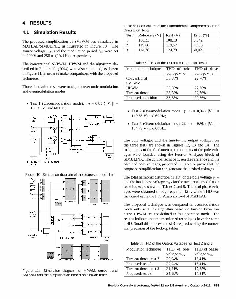
4 RESULTS
4.1 Simulation Results
The proposed simplification of SVPWM was simulated inMATLAB/SIMULINK, as illustrated in Figure 10. Thesource voltage vdc and the modulation period tm were setin 200 V and 250 us (1/4 kHz), respectively.
The conventional SVPWM, HPWM and the algorithm de-scribed in Filho et.al. (2004) were also simulated, as shownin Figure 11, in order to make comparisons with the proposedtechnique.
Three simulation tests were made, to cover undermodulationand overmodulation modes:
• Test 1 (Undermodulation mode): m = 0,85 (||Vr|| =108,23 V) and 60 Hz.;
�
Figure 10: Simulation diagram of the proposed algorithm.
�
Figure 11: Simulation diagram for HPWM, conventionalSVPWM and the simplification based on turn-on times.
Table 5: Peak Values of the Fundamental Components for theSimulation Tests.
Test Reference (V) Real (V) Error (%)1 108,23 108,18 0,0422 119,68 119,57 0,0953 124,78 124,78 -0,021
Table 6: THD of the Output Voltages for Test 1
Modulation technique THD of polevoltage vaN
THD of phasevoltage vaO
ConventionalSVPWM
38,58% 22,76%
HPWM 38,58% 22,76%Turn-on times 38,58% 22,76%Proposed algorithm 38,58% 22,76%
• Test 2 (Overmodulation mode 1): m = 0,94 (||Vr|| =119,68 V) and 60 Hz;
• Test 3 (Overmodulation mode 2): m = 0,98 (||Vr|| =124,78 V) and 60 Hz.
The pole voltages and the line-to-line output voltages forthe three tests are shown in Figures 12, 13 and 14. Themagnitudes of the fundamental components of the pole volt-ages were founded using the Fourier Analyzer block ofSIMULINK. The comparisons between the reference and theobtained pole voltages, presented in Table 6, prove that theproposed simplification can generate the desired voltages.
The total harmonic distortion (THD) of the pole voltage vaN
and the load phase voltage vaO for the mentioned modulationtechniques are shown in Tables 7 and 8. The load phase volt-ages were obtained through equation (2) , while THD wasmeasured using the FFT Analysis Tool of MATLAB.
The proposed technique was compared in overmodulationmode only with the algorithm based on turn-on times be-cause HPWM are not defined in this operation mode. Theresults indicate that the mentioned techniques have the sameTHD. Small differences in test 3 are produced by the numer-ical precision of the look-up tables.
Table 7: THD of the Output Voltages for Test 2 and 3
Modulation technique THD of polevoltage vaN
THD of phasevoltage vaO
Turn-on times: test 2 29,94% 16,41%Proposed: test 2 29,94% 16,41%Turn-on times: test 3 34,21% 17,35%Proposed: test 3 34,19% 17,31%
Revista Controle & Automação/Vol.22 no.5/Setembro e Outubro 2011 553

�
Figure 12: Test 1 (m = 0,85): Output voltages.
�
Figure 13: Test 2 (m = 0,94): Output voltages.
�
Figure 14: Test 3 (m = 0,98): Output voltages.
4.2 Experimental Results
The simplification of SVPWM based on the modified car-rier signal was implemented in the DSP DSPACE DS1104,which is programmable using SIMULINK block diagrams.
The proposed simplification was applied in the open-loopspeed control of an induction motor (3410 RPM, 60 Hz, 220Vrms, 0,5 HP). The driver IRAMX16UP60A was used as thetwo-level three-phase inverter.
Three experimental tests were done using the same character-istics of the simulation tests. The line-to-line voltages shownin Figures 15, 16 and 17 are similar to the respective wave-forms obtained in the simulation tests.
�
Figure 15: Test 1 (m = 0,85): Line-to-line voltage vab. Verticalscale: 100V/division.
�
Figure 16: Test 2 (m = 0,94): Line-to-line voltage vab. Verticalscale: 100V/division.
Figures 18, 19 and 20 show the stator currents of the motor.An evident distortion in the waveform of the stator currentappears in test 3, because the phase voltages which give en-
554 Revista Controle & Automação/Vol.22 no.5/Setembro e Outubro 2011
�
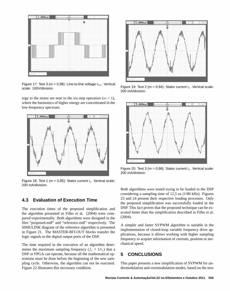
Figure 17: Test 3 (m = 0,98): Line-to-line voltage vab. Verticalscale: 100V/division.
ergy to the motor are near to the six-step operation (m = 1),where the harmonics of higher energy are concentrated in thelow-frequency spectrum.
�
Figure 18: Test 1 (m = 0,85): Stator current ia. Vertical scale:200 mA/division.
4.3 Evaluation of Execution Time
The execution times of the proposed simplification andthe algorithm presented in Filho et al. (2004) were com-pared experimentally. Both algorithms were designed in thefiles “proposed.mdl” and “reference.mdl” respectively. TheSIMULINK diagram of the reference algorithm is presentedin Figure 21. The MASTER-BIT-OUT blocks transfer thelogic signals to the digital output ports of the DSP.
The time required in the execution of an algorithm deter-mines the maximum sampling frequency (fs = 1/ts) that aDSP or FPGA can operate, because all the mathematical op-erations must be done before the beginning of the new sam-pling cycle. Otherwise, the algorithm can not be executed.Figure 22 illustrates this necessary condition.
�
Figure 19: Test 2 (m = 0,94): Stator current ia. Vertical scale:200 mA/division.
�
Figure 20: Test 3 (m = 0,98): Stator current ia. Vertical scale:200 mA/division.
Both algorithms were tested trying to be loaded in the DSPconsidering a sampling time of 12,5 us (1/80 kHz). Figures23 and 24 present their respective loading processes. Onlythe proposed simplification was successfully loaded in theDSP. This fact proves that the proposed technique can be ex-ecuted faster than the simplification described in Filho et al.(2004).
A simpler and faster SVPWM algorithm is suitable in theimplementation of closed-loop variable frequency drive ap-plications, because it allows working with higher samplingfrequency to acquire information of currents, position or me-chanical speed.
5 CONCLUSIONS
This paper presents a new simplification of SVPWM for un-dermodulation and overmodulation modes, based on the new
Revista Controle & Automação/Vol.22 no.5/Setembro e Outubro 2011 555

�
Figure 21: SIMULINK diagram of the SVPWM algorithm usedas reference.
��
Figure 22: Requirement to execute successfully an algorithmin a DSP.
�
Figure 23: Loading process of the reference SVPWM simpli-fication.
�
Figure 24: Loading process of the proposed SVPWM simpli-fication.
concept of the modified carrier signal. This technique uses asmall set of mathematical operations, while the sector iden-tification is made using reference pole voltages and only re-quires a small one-dimensional look-up table to operate inovermodulation mode. The proposed simplification has afaster execution time in DSPs than other simplifications inliterature, making possible the implementation of SVPWMalgorithm in DSPs or FPGAs using higher sampling frequen-cies, which is suitable in variable frequency drive applica-tions.
On the other hand, the proposed technique produces the sameswitching pattern that conventional SVPWM and HPWM.As a result, all these modulation technique produce the sameharmonic distortion and are affected for dead times in thesame way.
A future work consists in the use of the proposed simplifica-tion in a closed-loop speed control of three-phase motors.
REFERENCES
Bakhshai, A. R., Joos, G., Jain, P. K. and Jin, H. (2000).Incorporation the Overmodulation Range in Space Vec-tor Pattern Generators Using a Classification Algorithm,IEEE Transactions on Power Electronics, Vol. 15, No.1, pp. 83-91.
Blasko, V. (1997). A Hybrid PWM Strategy CombiningModified Space Vector and Triangle Comparison Meth-ods”, IEEE Transactions on Industry Applications, Vol.33, No. 3, pp. 756-764.
Bose, B. K., 2002, Modern Power Electronics and ACDrives, Prentice Hall PTR, New Jersey.
Cheng, C. 1999, Linear System Theory and Design, OxfordUniversity Press, third edition.
556 Revista Controle & Automação/Vol.22 no.5/Setembro e Outubro 2011

Filho, N. P., Pinto, J. O. P., Borges da Silva, L. E. andBose, B. K. (2004). A Simple and Ultra-Fast DSP-Based Space Vector PWM Algorithm and its Implemen-tation on a Two-Level Inverter Covering Undermodula-tion and Overmodulation, 30th Annual Conference ofIEEE Industrial Electronics Society, Vol. 2, pp. 1224-1229.
Hariram B. and Marimuthu, N. S. (2005). Space VectorSwitching Patterns for Different Applications - A Com-parative Analysis, IEEE International Conference on In-dustrial Technology, pp. 1444-1449.
Holmes, D. G. (1996). The Significance of Zero Space Vec-tor Placement for Carrier-Based PWM Schemes, IEEETransactions on Industry Applications, Vol. 32, No. 5,pp. 1122-1129.
Holtz, J. (1994). Pulsewidth Modulation for ElectronicPower Conversion, Proceedings of the IEEE, Vol. 82,No. 8, pp. 1194-1214.
Lamich, M., Balcells, J. and Gonzales, D. (2002). NewMethod for Obtaining SV-PWM Patterns Following anArbitrary Reference, 28th Annual Conference of the In-dustrial Electronics Society, Vol. 1, pp. 18-22.
Pinheiro. H, Botterón, F., Rech, C., Schuch, L., Camargo,R. F., Hey, H. L., Grundling, H. A. and Pinheiro, J. R.(2005). Modulação Space Vector para Inversores Ali-mentados em Tensão: Uma Abordagem Unificada, SBAControle e Automação, Vol. 16, No. 1, pp. 13-24.
Pinto, J. O. P., Bose B. K., Borges da Silva, L. E. andKazmierkowski, M. P. (2000). A Neural-NetworkBased Space-Vector PWM Controller for Voltage FedInverter Induction Motor Drive, IEEE Transactions onIndustry Applications, Vol. 36, No. 6, pp. 1628-1636.
Rashid, M. H., 2001, Power Electronics Handbook, Aca-demic Press.
Shu, Z., Tang, J., Guo, Y. and Lian, J. (2007). An Ef-ficient SVPWM Algorithm With Low ComputationalOverhead for Three-Phase Inverters, IEEE Transactionson Power Electronics, Vol. 22, No. 5, pp. 1997-1805.
Tzou, Y., and Hsu, H. (1997). FPGA Realization of Space-Vector PWM Control IC for Three-Phase PWM Invert-ers, IEEE Transactions on Power Electronics, Vol. 12,No. 6, pp. 953-963.
Van der Broek, H. W., Skudelny, H. C. and Stanke, G. V.(1988). Analysis and Realization of a Pulsewidth Mod-ulator Based on Voltage Space Vectors, IEEE Transac-tions on Industry Applications, Vol. 24, No. 1, pp. 142-150.
Yang, R., Wang, G., Yu, Y., Xu, D. and Chan, C. C. (2009).A Novel Space Vector Area Calculation Based Over-modulation Method,IEEE Vehicle Power and Propul-sion Conference, pp. 1399–1402.
Yu, Y., Chai, F. and Cheng, S. (2008). Analysis of Modula-tion Pattern and Losses in Inverter for PMSM Drives,IEEE Vehicle Power and Propulsion Conference, pp.1–4.
Yu, Z., 1999, Space-Vector PWM with TMS320C24x/F24xUsing Hardware and Software Determined SwitchingPatters. Application Report SPRA524, Texas Instru-ments.
Zhai, L. and Li, H. (2008) Modeling and Simulation ofSVPWM Control System of Induction Motor in ElectricVehicle, IEEE International Conference on Automationand Logistics, pp. 2026–2030.
Zhang, Y., Wang, S., Xia, H. and Ge, J. (2009). A NovelSVPWM Modulation Scheme, 24th Annual IEEE Ap-plied Power Electronics Conference and ExpositionAPEC 2009, pp. 128-131.
Revista Controle & Automação/Vol.22 no.5/Setembro e Outubro 2011 557


![A Comparative Study and Experimental Investigation of ...SVPWM, who contributed a lot in PWM methods [4-9]. In comparison between SPWM and SVPWM, SVPWM results excellent dc bus utilization](https://img.pdfslide.us/doc/110x75/61264de56b3f754d585eb80a/a-comparative-study-and-experimental-investigation-of-svpwm-who-contributed.jpg)