Embed Size (px)
Citation preview

HAL Id: lirmm-00838389https://hal-lirmm.ccsd.cnrs.fr/lirmm-00838389
Submitted on 25 Jun 2013
HAL is a multi-disciplinary open accessarchive for the deposit and dissemination of sci-entific research documents, whether they are pub-lished or not. The documents may come fromteaching and research institutions in France orabroad, or from public or private research centers.
L’archive ouverte pluridisciplinaire HAL, estdestinée au dépôt et à la diffusion de documentsscientifiques de niveau recherche, publiés ou non,émanant des établissements d’enseignement et derecherche français ou étrangers, des laboratoirespublics ou privés.
A New Recovery Scheme Against Short-to-LongDuration Transient Faults in Combinational Logic
Rodrigo Possamai Bastos, Giorgio Di Natale, Marie-Lise Flottes, Feng Lu,Bruno Rouzeyre
To cite this version:Rodrigo Possamai Bastos, Giorgio Di Natale, Marie-Lise Flottes, Feng Lu, Bruno Rouzeyre. A NewRecovery Scheme Against Short-to-Long Duration Transient Faults in Combinational Logic. Journal ofElectronic Testing, Springer Verlag, 2013, pp.001-010. �10.1007/s10836-013-5359-y�. �lirmm-00838389�
A New Recovery Scheme against Short-to-Long Duration Transient Faults in Combinational Logic
Rodrigo Possamai Bastos, Giorgio Di Natale, Marie-Lise Flottes, Feng Lu, and Bruno Rouzeyre LIRMM (Université Montpellier II / CNRS UMR 5506)
Montpellier, France {bastos, dinatale, flottes, lu, rouzeyre}@lirmm.fr
Abstract – This paper presents a new recovery scheme for dealing with short-to-long duration transient faults in combinational logic. The new scheme takes earlier into account results of concurrent error detection (CED) mechanisms, and then it is able to perform shorter recovery latencies than existing similar strategy. The proposed scheme also requires less memory resources to save input contexts of combinational logic blocks. In addition, this work also proposes a taxonomy of CED techniques. It allows pointing out which are the necessary recovery resources as well as identifying which are the types of CED mechanisms that can be used with the new recovery scheme of this paper. The effectiveness of the proposed scheme was evaluated through electrical-level simulations. For all short-to-long duration transient-fault injections, it was never slower than state-of-art similar strategy, and indeed its recovery latency was faster for 34% of the simulated faulty scenarios.
Keywords – transient faults; soft errors; concurrent error detection; and recovery schemes
I. INTRODUCTION
Higher resilience is expected from an increasing number of integrated systems while, in the same time, ultra-deep submicron technologies make these systems prone to misbehaviors induced by the natural aging processes or the environment (radiations from cosmic origin or every day material). In addition to these natural phenomena, malicious fault-based attacks can be used for leading secure systems to misbehavior, bypassing security mechanisms or providing information on confidential data [1][2]. For both these environmental or malicious phenomena many applications require fast recovery.
Until the early 2000’s, researches on transient faults and soft errors focused essentially on memory elements, which were considered the system’s most vulnerable circuits. Many concurrent error detection and/or correction mechanisms were proposed to mitigate soft errors induced by transient faults in memory cells. In the last decade, however, more sensitive deep-submicron technologies as well as the increasing demand in terms of digital security have also pushed for the development of countermeasures against transient faults in combinational parts of the circuits. These faults indeed can propagate up to storage elements and thus cause soft errors as well. On the other hand, if the transient fault does not induce any error due to an electrical, logical or latching-window masking effect, its detection is crucial all the same in secure applications since the fault itself reveals an attempt of attack.
In addition, some transient fault phenomena considered as short in the past (much less than one clock cycle) can be now considered as long duration transient faults (reaching the clock period) due to the possibility of higher operating frequencies in recent ultra-deep-submicron technology-based circuits [3][4]. In fact, the effects of long-duration transient faults have clearly a much higher probability of not being masked, and so they also stand a greater chance of producing system failures. In addition, we may expect that maliciously induced transients could be better monitored whether they last several clock cycles. This emerging issue on long-duration transients introduces therefore supplementary difficulties to design optimized protections for the circuits.
The current trend in solutions to cope with transient-fault effects is applying protection techniques at different abstraction levels of the design [3][4][5][6]. The idea is thus to prevent the use of costly fault-tolerance mechanisms like the tripe modular redundancy, taking advantage of cheaper mitigation techniques that ensure satisfactory soft-error coverage for the system’s most recurrent operations. This modern strategy is exemplified through recovery schemes based on concurrent error detection (CED).
CED mechanisms designed at transistor or gate level guarantee an early detection, as soon as the faults happens, preventing more critical failure scenarios such as the induction and propagation of multiple errors to other clock cycles, stages, or parts of the system. In case of misbehavior, an error flag is generated and the scheme can activate recovery mechanisms already implemented in modern systems for dealing with branch misprediction [4][6]. After the transient fault disappearing, earlier faulty operation is thus repeated and the system returns to perform its normal computational sequence.
This work proposes a new recovery scheme based on CED that can be also used to improve already existing solutions. More precisely, the contributions of this paper are:
• Section II presents a new taxonomy of CED techniques that allows understanding the requirements for implementing their associated recovery schemes against short-to-long duration transient faults as well as evaluating qualitatively their costs and efficiencies;
• Section III discusses recovery schemes at micro-architectural level in function of the CED types defined in section II. Furthermore, we show a transient-fault scenario that proves for existing recovery schemes the exigency of saving two input contexts of logic blocks;

• Section IV presents the new recovery scheme and, unlike our work in [7], its generic applicability for any CED technique classified in II as asynchronous due to its transient result in function of the fault behavior;
• Section V evaluates the effectiveness of our scheme and compares it with another existing similar strategy. We show the benefits of the new recovery scheme based on experimental results issued from transient-fault injection simulations.
II. TYPES OF CED TECHNIQUES
In the following, CED (Concurrent Error Detection) is a misuse of language because we consider error detection and fault detection schemes as well. As mentioned before, transient faults do not necessarily produce a soft error; however detection of masked transient faults is also of importance for secure applications.
Classic CED solutions to face transient-fault effects are adding spatial, information, or time redundancy to the circuit. These three approaches can be implemented at different abstraction levels of the design. Fig. 1 presents basic example of such techniques at micro-architectural level. They essentially compare two redundant results of which at least one must be safe to permit the detection of errors. If for instance one result fails, the comparison provides an error flag. Furthermore, Fig. 1 also illustrates another type of CED that is based on built-in current sensors (BICS). BICS are connected either to Vdd and Gnd (VGBICS in [8]) or to Bulks of transistors (BBICS in [9]) in order to detect anomalous transient currents that can become (or not) soft errors. BICS-based schemes therefore are able to generate an error flag in case of occurrence of transient faults within a range defined by the calibration of the BICS.
Fig.2 generalizes the components of a CED with recovery to protect a target circuit. The CED circuitry is responsible to deliver an error flag if a transient misbehaviour is detected (i.e. a transient fault in the combinational logic of the target circuit or a soft error in a storage element). However, as such an error flag can have behaviours as transient and asynchronous as the transient fault that induces it, mechanisms for sampling this CED’s result have to be implemented. These sampling mechanisms ensure the error flags in a steady state enough time to activate correctly the recovery procedure.
If we come back to the columns of Fig. 1, we can even classify the CED techniques into two types according to the features of their error flags:
• Synchronous CED schemes: classic CED approaches that compare their redundant parts after the data register (e.g. [10][11][12][13][14]). Hence, they inherently guarantee their results in steady conditions during the cycle following the cycle on which the transient fault appears. The error flag is generated already in synchronization with the system since the mechanisms for sampling such a CED’s result are indeed parts of the CED scheme. Therefore, there is no need for registering this result if its value is directly used for starting the recovery procedure during the cycle following the first faulty cycle. On the other
hand, only transient faults that reach data registers (causing soft errors) are detected in this case. As discussed before, it is correct for applications in which the recovery must be launch only in case of soft errors, but this is not sufficient when transient faults must be detected even if they do not induce any error. Synchronous CED schemes can be very expensive since they require the storage of all redundant data bits (N or C additional redundant registers in Fig. 1’s examples) [15];
• Asynchronous CED schemes: CED techniques that
generate asynchronously their error flags in function of the transient-fault features (e.g. [4][6][8][9][16][17] [18][19][20]). Hence, asynchronous CED schemes must include another extra 1-bit register dedicated only to sample their error flags, and so ensuring results at steady state during the necessary time for starting the recovery procedures. Conversely to synchronous CED schemes, there is no need to register the redundant data bits but only the flag, and thus these solutions are less expensive [15].
Figure 1. Examples of synchronous and asynchronous CED schemes
Figure 2. A target circuit protected by using CED with recovery
III. RECOVERY SCHEMES FOR DEALING WITH SHORT AND
LONG-DURATION TRANSIENT FAULTS IN LOGIC
CED techniques dedicated to identify transient-fault effects require recovery schemes in order to correct soft errors. The recovery machine acts in function of the CED’s result to thus in fault-free conditions repeat the affected cycles whether an error flag is generated.
The recovery scheme, therefore, initially works to save fault-free input status of the target circuit, such as input values of logic blocks. Then, in case of an error flag, the system is able to later reload such good input values (after the transient fault vanishing), and so recomputing the first cycle at which the fault has affected the logic block’s operations.
We highlight that there is a latency of extra clock cycles only if a transient fault is detected, and thus the target circuit normally operates without penalty in fault-free scenarios. About the area overheads added by recovery schemes we remind that they can be minimal whether the target circuit’s architecture has already a machine to repeat operations in branch-misprediction situations. In addition, microprocessor-based systems can take advantage of their instruction/data memory resources in order to save the input context of logic blocks.
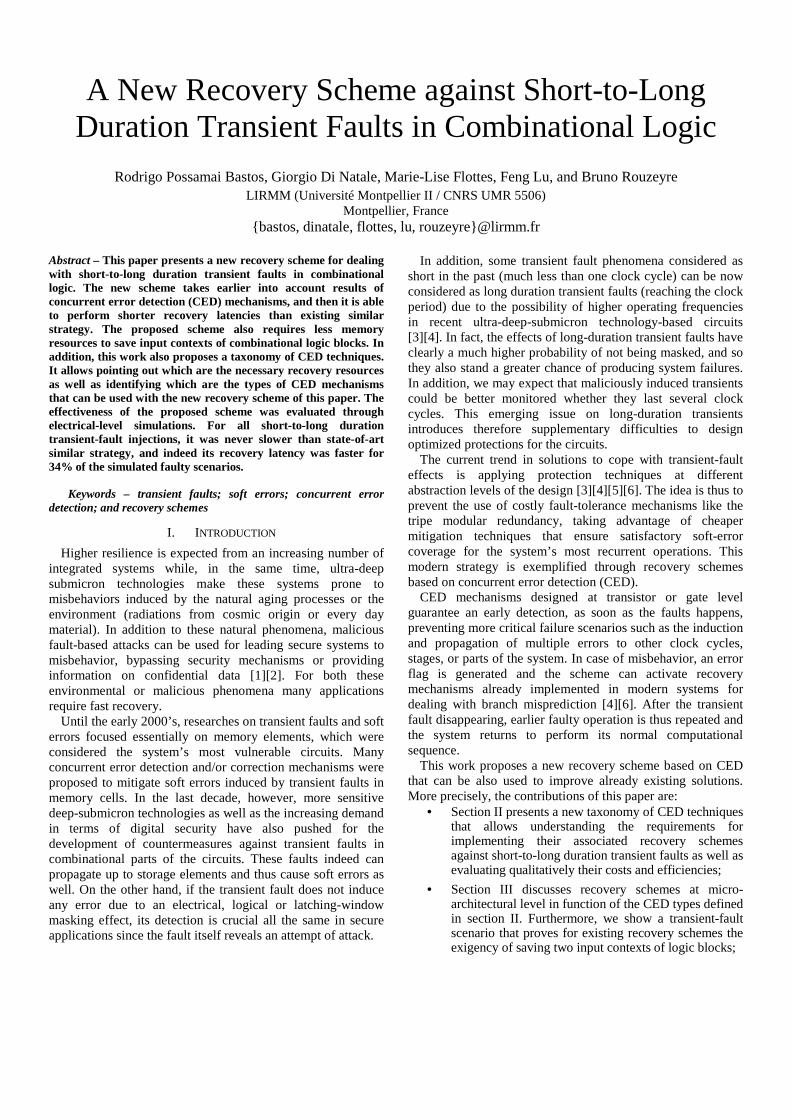
Fig. 3, 4, and 5 illustrate a system compounded of a register IN, a register OUT, and a logic block that is protected by three different recovery schemes for dealing with short and long duration transient faults. The other grey blocks (i.e. except CED schemes, Redundant, Fault and Recovery Registers, and Reset multiplexer) are resources that might be already present in certain modern architectures to recompute previous operations, and so they can be reused in conjunction with CED schemes to mitigate transient faults. Note in Fig. 3, 4, and 5 that the communications between the CED blocks and the recovery circuits are slightly different. More precisely, the type of CED scheme (Synchronous or Asynchronous, as section II defines) and the strategy for sampling its results (e.g. by using a Flip-Flop or a Latch) determine the recovery efficiency and which minimum memory resources are necessary to properly save input contexts of logic blocks during the fault-free cycles that precede the first faulty cycle “First_Faulty_Cycle”.
The costly synchronous CED techniques discussed in II require at least a recovery scheme similar to Fig. 3’s illustration. This classic machine saves the logic block’s inputs during each clock’s low phase by using a memory that, in this example, is represented by K latches, and we call it in this paper as a backup file. Then, when the CED scheme indicates an error flag in the cycle posterior to “First_Faulty_Cycle”, the machine is able to restore the saved logic block’s inputs (Fig. 3’s “saved_logic_inputs”) of one cycle ago the instant at which the error flag is set (i.e. the logic block’s inputs of “First_Faulty_Cycle”). This process of restoring and recomputing is done in the first following fault-free cycle “Repeated_Cycle” on which the transient fault has already vanished.
Asynchronous CED techniques that use a flip-flop for sampling its results demand a recovery scheme like the schematic in Fig. 4 (e.g. [6]’s Checksum-based scheme). This simple strategy is not so efficient to sample the CED’s results [15][21], and then its recovery efficiency is moderate.
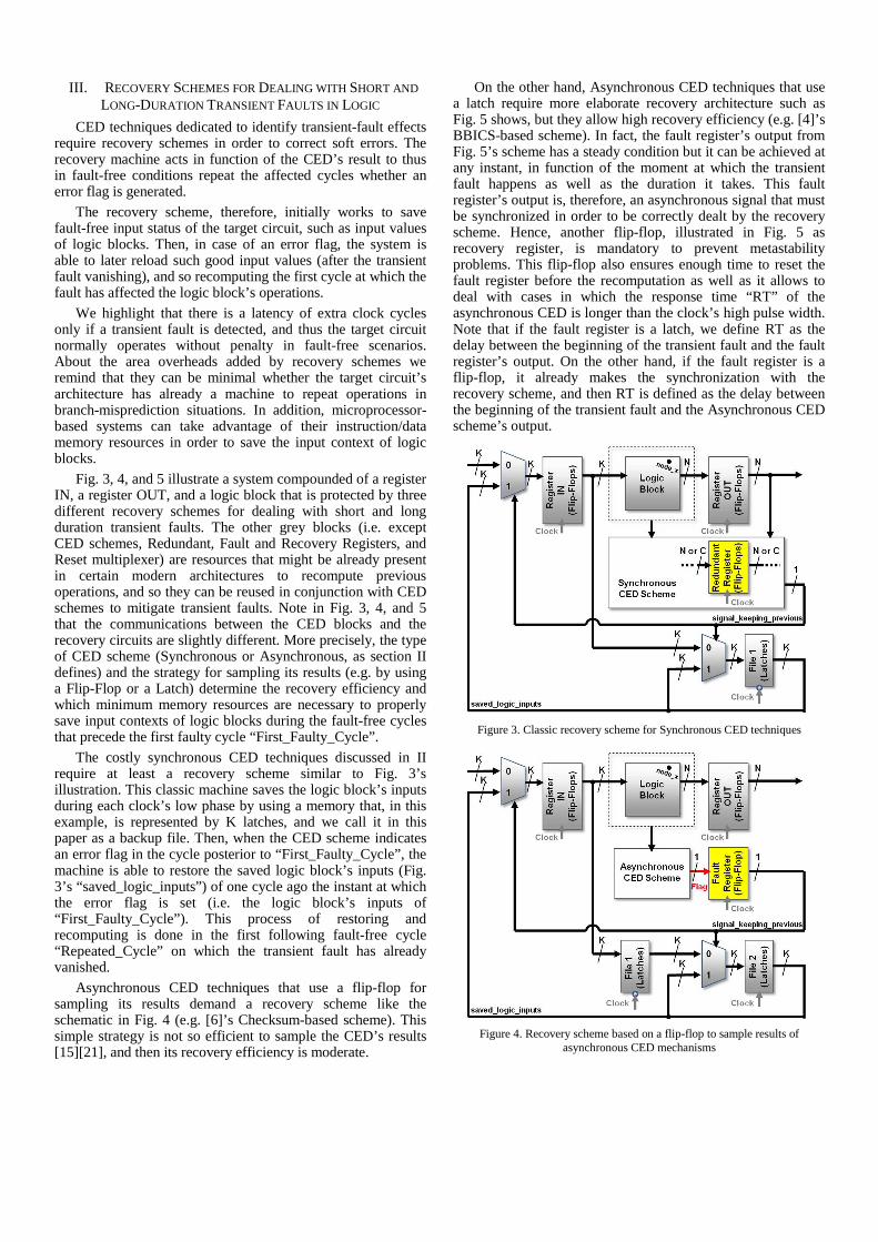
On the other hand, Asynchronous CED techniques that use a latch require more elaborate recovery architecture such as Fig. 5 shows, but they allow high recovery efficiency (e.g. [4]’s BBICS-based scheme). In fact, the fault register’s output from Fig. 5’s scheme has a steady condition but it can be achieved at any instant, in function of the moment at which the transient fault happens as well as the duration it takes. This fault register’s output is, therefore, an asynchronous signal that must be synchronized in order to be correctly dealt by the recovery scheme. Hence, another flip-flop, illustrated in Fig. 5 as recovery register, is mandatory to prevent metastability problems. This flip-flop also ensures enough time to reset the fault register before the recomputation as well as it allows to deal with cases in which the response time “RT” of the asynchronous CED is longer than the clock’s high pulse width. Note that if the fault register is a latch, we define RT as the delay between the beginning of the transient fault and the fault register’s output. On the other hand, if the fault register is a flip-flop, it already makes the synchronization with the recovery scheme, and then RT is defined as the delay between the beginning of the transient fault and the Asynchronous CED scheme’s output.
Figure 3. Classic recovery scheme for Synchronous CED techniques
Figure 4. Recovery scheme based on a flip-flop to sample results of asynchronous CED mechanisms
Both types of machine in Fig. 4 and 5 save logic block’s
inputs of two clock cycles by using two backup files with K latches each one. Thereby, if CED scheme indicates an error flag, the recovery circuit is able to restore in “Repeated_Cycle” the saved logic block’s inputs (Fig. 4 and Fig 5.’s “saved_logic_inputs”) of two cycles ago the instant at which the error flag is identified and registered at “signal_keeping_previous”. Observe in Fig. 4 and 5 that this signal is used to keep in the backup files the logic block’s inputs of the previous cycles.
We notice in this paper that recovery strategies such as Fig. 4 and Fig. 5’s schemes necessarily need at least two backup files with K latches to save logic block’s inputs of two clock cycles. In fact, as Fig. 6 highlights, there are chances of transient faults “TF” starting in cycle 1 not to raise “signal_keeping_previous” in cycle 2, and then the logic block’s inputs saved in file 1 during cycle 1 must be transferred to file 2 during cycle 2 in order to be available in cycle 3. Furthermore, if the response time “RT” is greater than the clock period “T” (e.g. [4]’s BBICS calibrated with slower RT), more than two files are required. Therefore, the slower the RT the greater can be the number of required files.
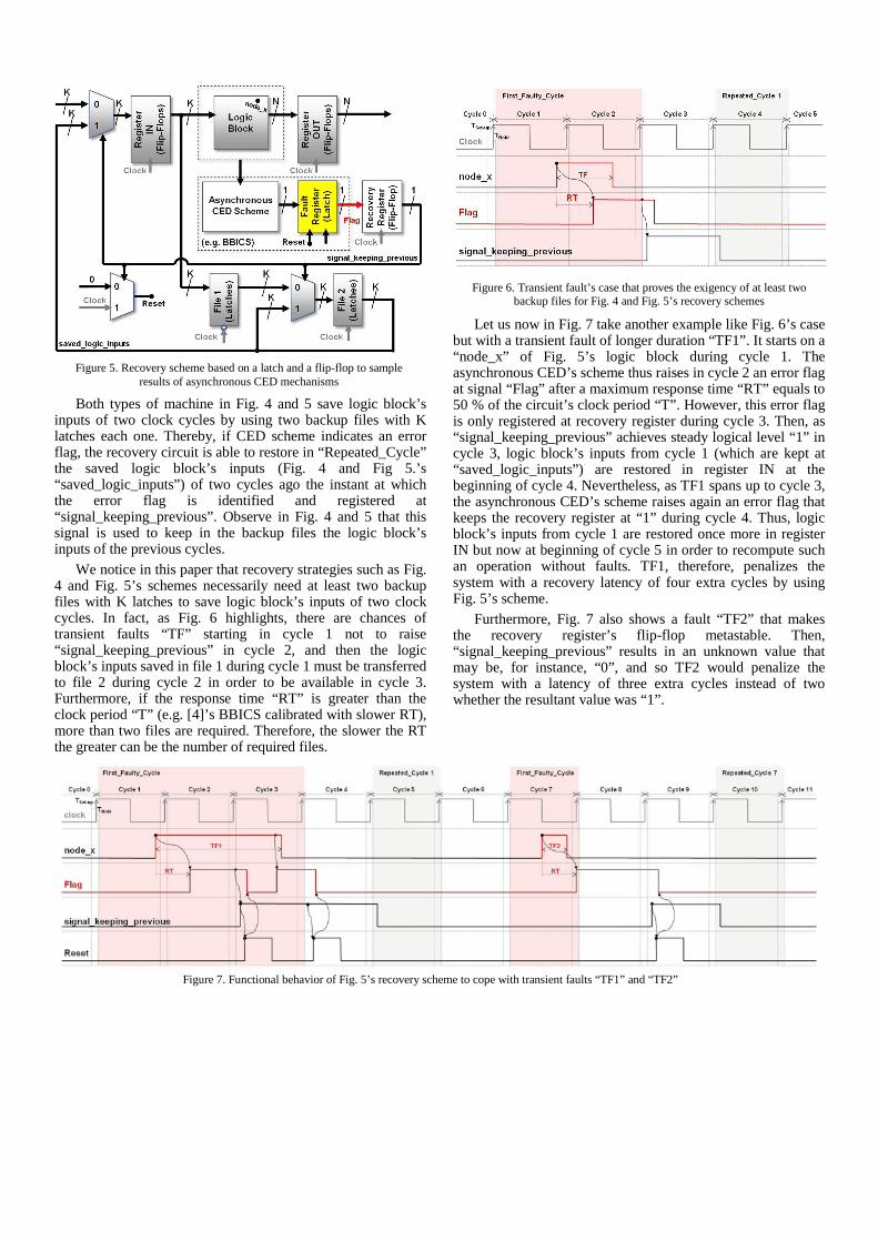
Let us now in Fig. 7 take another example like Fig. 6’s case
but with a transient fault of longer duration “TF1”. It starts on a “node_x” of Fig. 5’s logic block during cycle 1. The asynchronous CED’s scheme thus raises in cycle 2 an error flag at signal “Flag” after a maximum response time “RT” equals to 50 % of the circuit’s clock period “T”. However, this error flag is only registered at recovery register during cycle 3. Then, as “signal_keeping_previous” achieves steady logical level “1” in cycle 3, logic block’s inputs from cycle 1 (which are kept at “saved_logic_inputs”) are restored in register IN at the beginning of cycle 4. Nevertheless, as TF1 spans up to cycle 3, the asynchronous CED’s scheme raises again an error flag that keeps the recovery register at “1” during cycle 4. Thus, logic block’s inputs from cycle 1 are restored once more in register IN but now at beginning of cycle 5 in order to recompute such an operation without faults. TF1, therefore, penalizes the system with a recovery latency of four extra cycles by using Fig. 5’s scheme.
Furthermore, Fig. 7 also shows a fault “TF2” that makes the recovery register’s flip-flop metastable. Then, “signal_keeping_previous” results in an unknown value that may be, for instance, “0”, and so TF2 would penalize the system with a latency of three extra cycles instead of two whether the resultant value was “1”.
Figure 5. Recovery scheme based on a latch and a flip-flop to sample results of asynchronous CED mechanisms
Figure 6. Transient fault’s case that proves the exigency of at least two backup files for Fig. 4 and Fig. 5’s recovery schemes
Figure 7. Functional behavior of Fig. 5’s recovery scheme to cope with transient faults “TF1” and “TF2”
IV. A NEW RECOVERY SCHEMES FOR DEALING WITH
SHORT AND LONG-DURATION TRANSIENT FAULTS IN LOGIC
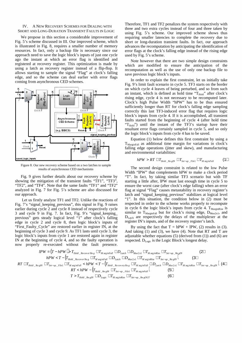
We propose in this section a considerable improvement of Fig. 5’s scheme discussed in III. Our improved scheme, which is illustrated in Fig. 8, requires a smaller number of memory resources. In fact, only a backup file is necessary since our approach need to save the logic block’s inputs of just one cycle ago the instant at which an error flag is identified and registered at recovery register. This optimization is made by using a latch as recovery register instead of a flip-flop. It allows starting to sample the signal “Flag” at clock’s falling edge, and so the scheme can deal earlier with error flags coming from asynchronous CED schemes.
Fig. 9 gives further details about our recovery scheme by
showing the mitigation of the transient faults “TF1”, “TF3”, “TF2”, and “TF4”. Note that the same faults “TF1” and “TF2” analyzed in Fig. 7 for Fig. 5’s scheme are also discussed for our approach.
Let us firstly analyze TF1 and TF2. Unlike the reactions of Fig. 7’s “signal_keeping_previous”, this signal in Fig. 9 raises earlier during cycle 2 and cycle 8 instead of respectively cycle 3 and cycle 9 in Fig. 7. In fact, Fig. 9’s “signal_keeping_ previous” gets steady logical level “1” after clock’s falling edge in cycle 2 and cycle 8, then logic block’s inputs of “First_Faulty_Cycle” are restored earlier in register IN, at the beginning of cycle 3 and cycle 9. As TF1 lasts until cycle 3, the logic block’s inputs from cycle 1 are restored again in register IN at the beginning of cycle 4, and so the faulty operation is now properly re-executed without the fault presence.
Therefore, TF1 and TF2 penalizes the system respectively with three and two extra cycles instead of four and three taken by using Fig. 5’s scheme. Our improved scheme shows thus requiring smaller latencies to complete the recovery due to short or long-duration transient faults. In fact, our approach advances the recomputation by anticipating the identification of error flags at the clock’s falling edge instead of the rising edge used by Fig. 5’s scheme.
Note however that there are two simple design constraints which are modified to ensure the anticipation of the recomputation as well as the use of only one backup file to save previous logic block’s inputs.
In order to explain the first constraint, let us initially take Fig. 9’s limit fault scenario in cycle 5. TF3 starts on the border on which cycle 4 leaves of being perturbed, and so from such an instant, which is defined as hold time “THold” after clock’s rising edge, cycle 4 is not necessary to be recomputed later. Clock’s high Pulse Width “hPW” has to be thus ensured sufficiently longer than RT for clock’s falling edge sampling correctly this last TF3-induced error flag that requires logic block’s inputs from cycle 4. If it is accomplished, all transient faults started from the beginning of cycle 4 (after hold time “T Hold”) until the instant of the TF3’s startup have their resultant error flags certainly sampled in cycle 5, and so only the logic block’s inputs from cycle 4 has to be saved.
Equation (1) below defines this first constraint by using a TMarginFall as additional time margin for variations in clock’s falling edge operations (jitter and skew), and manufacturing and environmental variabilities:
inFallMFileupSetgINHold TTTRThPW arg1_Re_ +++> − (1)
The second design constraint is related to the low Pulse Width “lPW” that complements hPW to make a clock period “T”. In fact, by taking similar TF3 scenario but with TF starting a little after, lPW must last enough time in cycle 5 to ensure the worst case (after clock’s edge falling) when an error flag at signal “Flag” causes metastability in recovery register’s latch and “signal_keeping_previous” stabilizes at logical level “1”. In this situation, the condition below in (2) must be respected in order to the scheme works properly to recompute in cycle 6 the logic block’s inputs from cycle 4. TMarginRise is similar to TMarginFall but for clock’s rising edge, DMux2x1, and DLatch are respectively the delays of the multiplexer at the register IN’s inputs, and of the recovery register’s latch.
By using the fact that T = hPW + lPW, (2) results in (3). And taking (1) and (3), we have (4). Note that RT and T are adjustable whether equations (5) (derived from (1)) and (6) are respected. DLogic is the Logic Block’s longest delay.
( ) gINupSetinRiseMxMuxLatchinFallMgerHold TTDDTThPWTlPW Re_arg12argRecovRe_ −+++++>−= (2)
( )gINupSetinRiseMxMuxLatchinFallMgerHold TTDDTTThPW Re_arg12argRecovRe_ −+++++−<
(3) ( )gINupSetinRiseMxMuxLatchinFallMgeryHoldinFallMFileupSetgINHold TTDDTTThPWTTTRT Re_arg12argRecovRe_arg1_Re_ −− +++++−<<+++ (4)
( )inFallMFileupSetgINHold TTThPWRT arg1_Re_ ++−< − (5)
gOUTupSetinRiseMLogicgINHold TTDTT Re_argRe_ −+++> (6)
Figure 8. Our new recovery scheme based on a two latches to sample results of asynchronous CED mechanisms

V. EXPERIMENTAL RESULTS COMPARING RECOVERY
SCHEMES
In this section we present some experimental results that show the effectiveness of our proposed approach. We compare the recovery latency required for the schemes presented in Fig. 5 and Fig. 8 (our proposed solution). Fig. 3 and Fig. 4’s schemes are not considered because the first one is very costly in terms of area and power consumption while Fig. 4’s approach is not so effective in identifying many transient-fault scenarios and requires at least two backup files (see discussions in sections II and III). Furthermore, in theory these schemes in Fig. 3 and Fig. 4 have higher recovery latencies or, at the best, equivalent since they sample the error flags by using the same clock’s edge used by register IN and OUT.
Experimental results were obtained using hspice simulation of circuits with the recovery schemes and of the injected single transient fault. The asynchronous CED scheme and the fault register’s latch from Fig. 5 and Fig. 8 were emulated such as the behavior of BBICS. The following parameters were considered:
• The circuits were designed using a 65-nm standard-cell library (ST CORE65LPSVT), Vdd 1.2V, and nominal conditions;
• The clock period is 1ns, 50 % duty cycle;
• The transient fault was simulated by using a double-exponential current source. Then, transient pulses with several durations (50ps, 250ps, 500ps, 750ps, and 1ns) were parameterized in such a way that the voltage amplitude achieves Vdd. It prevents the electrical masking effects of the transient faults. In fact, as the goal is to analyze the efficiency of the recovery mechanisms and not of the CED techniques, we were
not interested in any type of transient-fault masking effect;
• Considered RT (asynchronous CED’s response time defined in III) are 200ps, 250ps, 300ps, and 400ps;
• Initial instant of injection were simulated from 0 to 1000 ps of “First_Faulty_Cycle”. We have therefore supposed a range of different logic block’s nodes on which single transient faults are injected and propagated up to make a soft error in register OUT. Logical and latching-window masking effects of the transient faults are thus not taken into account. As a step of 1ps is used, 1000 simulations were performed for each value of RT and fault duration;
• Recovery latency is expressed in number of clock cycles required for the scheme to recompute the logic block’s inputs of “First_Faulty_Cycle”.
For each RT values and transient fault durations, we have counted how many injections (over 1000) were recovered in 1, 2, 3, and 4 clock cycles. Results of all simulations are summarized in Fig. 10. As it can be seen, our proposed scheme allows recovering from short and long transient faults in less clock cycles than the other solution. For instance, for RT 400ps and fault duration 1000ps, our Fig. 8’s approach has a recovery latency of 4 cycles in 21% of the injected faults and of 3 cycles in the remainder 79%, while Fig. 5’s scheme requires 4 cycles in 73% of the injected faults and of 3 cycles in 27% of the scenarios.
Finally, taking into account all transient fault durations for RT 200ps, 250ps, 300ps, and 400ps, the circuit with our scheme returned to its normal operation one cycle earlier respectively in 31%, 33%, 35%, and 37% of the injected transient-fault scenarios. Note therefore that the slower the RT the better is our solution. Evidently, in the remainder of the scenarios both schemes have the same recovery latency.
Figure 9. Functional behavior of our new recovery scheme to cope with transient faults “TF1”, “TF3”, “TF2”, and “TF4”

VI. FINAL CONCLUSIONS
In this paper we have proposed the classification of the CED techniques into synchronous and asynchronous in order to identify which are the necessary recovery resources. In addition, we have proposed a new recovery scheme based on asynchronous CED schemes for dealing with short-to-long transient faults. Our approach uses the clock’s falling edges (in case of data registers use clock’s rising edges) for starting to sample error flags from transient faults. It allows reducing the recovery latency by one cycle. Moreover, the new recovery scheme also permits to use only a backup file to save input contexts of logic blocks. Our solution therefore requires much smaller recovery resources and lower latency than existing similar strategy.
REFERENCES [1] C.N. Chen, and S.M. Yen, “Differential Fault Analysis on AES Key
Schedule and Some Countermeasures,” in Proc. ACISP, v. 2727 of LNCS, 2003, pp. 118-129.
[2] P. Dusart, G. Letourneux, and O. Vivolo, “Differential Fault Analysis on A.E.S,” in Proc. ACNS, v. 2846 of LNCS, 2003, pp. 293-306.
[3] C. Lisboa, M. Erigson, and L. Carro, “System level approaches for mitigation of long duration transient faults in future technologies,” in Proc. ETS, IEEE, 2007, pp. 165-170.
[4] C. Lisboa et al., “Using Built-in Sensors to Cope with Long Duration Transient Faults in Future Technologies,” in Proc. ITC, IEEE, 2007, pp. 1-10.
[5] C. Albrecht et al., “Towards a Flexible Fault-Tolerant System-on-Chip,” in Proc. ARC, VDE Verlag GMBH, 2009, pp. 83-90.
[6] S. Z. Shazli, and M. B. Tahoori, “Transient Error Detection and Recovery in Processor Pipelines,” in Proc. DFT, IEEE, 2009, pp. 304-312.
[7] R.P. Bastos, G.D. Natale, M. Flottes, and B. Rouzeyre, “A New Bulk Built-In Current Sensor-Based Strategy for Dealing with Long-Duration Transient Faults in Deep-Submicron Technologies,” in Proc. DFT, IEEE, 2011, pp. 302-308.
[8] B. Gill et al., “An Efficient BICS Design for SEUs Detection and Correction in Semiconductor Memories,” in Pro. DATE, IEEE, 2005, pp. 592-597.
[9] E. H. Neto et al., “Using Bulk Built-in Current Sensors to Detect Soft Errors,” IEEE Micro, v. 26, n. 5, pp. 10–18, Sep. 2006.
[10] S. Mitra and E. McCluskey, “Which concurrent error detection scheme to choose?,” in Proc. ITC, IEEE, 2000, pp. 985–994.
[11] M. Nicolaidis, “Time redundancy based soft-error tolerance to rescue nanometer technologies,” in Proc. VTS, IEEE, 1999, pp. 86-94.
[12] Anghel, L., and M. Nicolaidis, “Cost Reduction and Evaluation of a Temporary Faults Detecting Technique,” in Proc. DATE, IEEE, 2000, pp. 591-598.
[13] D. Ernst et al., “Razor: A low-power pipeline based on circuit-level timing speculation,” in Proc. MICRO, IEEE/ACM, 2003, pp. 7-18.
[14] K. Bowman et al., “Energy-efficient and metastability-immune resilient circuits for dynamic variation tolerance,” IEEE JSSC, v. 44, n. 1, pp. 49–63, Jan. 2009.
[15] R. P. Bastos et al., “How to Sample Results of Concurrent Error Detection Schemes in Transient Fault Scenarios?,” in Proc. RADECS, IEEE, 2011, pp. 635-642.
[16] S. Das et al., “RazorII: In situ error detection and correction for PVT and SER Tolerance,” IEEE JSSC, vol. 44, no. 1, pp. 32–48, Jan. 2009.
[17] M. M. Kermani, A. R. Masoleh, “Parity-Based Fault Detection Architecture of S-box for Advanced Encryption Standard,” in Proc. DFT', IEEE, 2006, pp. 572-580.
[18] C. Lisboa, and L. Carro, “XOR-based low cost checkers for combinational logic,” in Proc. DFT, IEEE, 2008, pp. 281-289.
[19] D. Rossi, M. Omanã, and C. Metra, “Transient fault and soft error on-die monitoring scheme,” in Proc. DFT, IEEE, 2010, pp. 391–398.
[20] D. J. Palframan, N. S. Kim, M. H. Lipasti, “Time Redundant Parity for Low-Cost Transient Error Detection,” in Proc. DATE, IEEE, 2011.
[21] R. P. Bastos et al., “Timing Issues for an Efficient Use of Concurrent Error Detection Codes,” in Proc. LATW, IEEE, 2011, pp. 1-6.
Figure 10. Distribution of recovery latencies (1, 2, 3, or 4 clock cycles) for Fig. 8 and Fig. 5’s recovery schemes in function of the asynchronous CED’s response time “RT” (200ps, 250ps, 300ps, and 400ps) and the transient fault duration (50ps, 250ps, 500ps, 750ps, and 1ns). For instance, let us take RT
200ps and fault duration 50ps, our Fig. 8’s approach has a recovery latency of 1 cycle in 26% of the injected faults and of 2 cycles in the remainder 74%, while Fig. 5’s scheme requires 3 cycles in 27% of the injected faults and of 2 cycles in 73% of the scenarios.