Embed Size (px)
Citation preview

A New Lab for 6.111:A Coin operated Vending Machine Controller
by
Calvin J. Lin
Submitted to the Department of Electrical Engineering andComputer Science
in Partial Fulfillment of the Requirements for the Degree of
Master of Engineering in Electrical Engineering and Computer Science
at the
MASSACHUSETTS INSTITUTE OF TECHNOLOGY
May 19, 1999
Copyright © 1999 Calvin J. Lin. All rights reserved.
The author hereby grants to M.I.T. permission to reproduceand distribute publicly paper and electronic copies of this thesis and to
grant others the right to do so.
Author.Department of Electrical Engineering an Computer Science
May 21, 1999
Certified byDonald E. Troxel
Thesis Spervisor
Accepted by -
Arthur C. SmithChairman, Department Committee on Graduate Theses
0
ENSLIBRARIES

An New Lab for 6.111:A Coin Operated Vending Machine Controller
by
Calvin J. Lin
Submitted to the Department of Electrical Engineering and Computer Science
May 21, 1999
In Partial Fulfillment of the Requirements for the Degree ofMaster of Engineering in Electrical Engineering and Computer Science
Abstract
This new lab was designed for the purpose of updating the curriculum of MIT's digitaldesign course, 6.111 Introductory Digital Systems Lab. The subject of the laboratoryassignment is the construction of a coin operated vending machine controller. It requiresstudents to design, build and debug this controller using current technology available inthe 6.111 lab. Because this is the first design exercise for most students, the assignment isstructured in a manner appropriate for teaching the design process Students gain practicalexperience in designing a real digital system using industry based tools and standards. Itis expected that completion of this lab will prepare the students for subsequent labs and afinal project.
Thesis Advisor: Donald E. TroxelTitle: Professor
2

Acknowledgments
This thesis would not have been completed if I did not receive the help and supportfrom several people. First are the students who patiently undertook the first iteration ofthis assignment. I know I gave them a hard lab to complete and hope they were able togain the knowledge I wanted to impart.
I would also like to thank the staff of 6.111 whom I had the good fortune to cometo know during my brief time with the class. Not only did they give me great suggestionson how to improve this lab, but kept me company when I was helping students into theearly hours of the morning.
I would like to thank my family for giving me the opportunity and instilling in methe drive to complete my education at MIT. Don't worry Mom and Dad, your moneyhasn't gone to waste.
Finally, I would like to thank my friends for making the time I've spent here veryenjoyable. They not only supported me in my classwork, but they also made sure I hadfun while I was here.
3

Table of Contents
1 Overview ........................................................... 9
2 Background........................................................11
2.1 U pdating 6.111.................................................. 11
2.1.1 Previous W ork ............................................ 12
2.1.2 W ork Since............................................... 12
2.2 Problem Statem ent............................................... 12
2.2.1 Testing and Verification..................................... 13
2.2.2 Flexibility ................................................ 13
2.2.3 Bridge for Lab Three....................................... 13
2.3 D esign G oals ................................................... 14
2.3.1 Educational Goals ......................................... 14
2.3.2 Scope of Project........................................... 15
3 Design of the Laboratory Assignment...................................16
3.1 Vending Machine Operation ...................................... 16
3.2 Organizing the Assignment ....................................... 17
3.2.1 Design Review........................................... 17
3.2.2 Building the Project ....................................... 18
3.2.3 Laboratory Report ........................................ 18
3.3 Satisfying Design Criteria ........................................ 19
3.3.1 Educational Goal ........................................ 19
3.3.2 Scope of Project.......................................... 20
4

4 A Discussion on Implementation...........
4.1 Initial Problems ......................
4.1.1 Fitting.......................
4.1.2 Testing ......................
4.2 Student Feedback....................
4.2.1 Software vs. Hardware ..........
4.2.2 Learning VHDL ...............
4.2.3 Difficulty Compared to Lab Three.
4.3 Modifications to the Lab ..............
4.3.1 More Structured Assignment .....
4.3.2 Testing Eliminated .............
4.4 Future W ork ........................
4.4.1 Testing and Verification .........
4.4.2 More Modifications ............
4.4.3 An Interactive Demo ...........
4.4.3 Designing a New Lab...........
5 The Laboratory Handout...
6 A Sample Solution.........
6.1 Clock Generator.......
6.2 Memory Storage Unit . .
6.3 CPLD ...............
6.3.1 Synchronizer ...
6.3.2 Accumulator ....
6.3.3 FSM ..........
7 Checkoff Guidelines......
8 Conclusion..............
. .21
................. 2 1
................. 2 1
................. 22
................. 22
................. 23
................. 23
................. 23
................. 23
................. 24
................. 24
................. 25
................. 25
................. 25
................. 26
................. 26
.. . . . . . . . . . . . . . . . . . . .. 27
. .37
.. 37
.. 38
.. 38
.. 40
.. 40
.. 41
44
. . . . . . . . . . . . . . . . . . . . .. 47
5
........................................... 0 0 0 0 0 0 0

A Listing of Code Provided to Students ................................... 49
A. 1 Example FSM : lab2.vhd ............................. ............. 49
B Listing of Code Used in the Sample Solution.............................51
B.1 Synchronizer Code: sync.vhd .................................... 51
B.2 Accumulator Code: accum.vhd ..................................... 52
B.3 FSM Code: vendcont.vhd ..................... .................... 53
6

List of Figures
5.1 Vending Machine Top Level Controller Block Diagram.................. 29
5.2 System Level Block Diagram .................................... 30
5.3 SRAM Address Timing ......................................... 35
6.1 Clock Generator Schematic ...................................... 38
6.2 CPLD and SRAM Schematic ..................................... 39
6.3 Synchronizer Block Diagram and Timing ............................ 40
6.4 Accumulator Block Diagram ...................................... 41
6.5 FSM State Transition Diagram ................................... 42
7
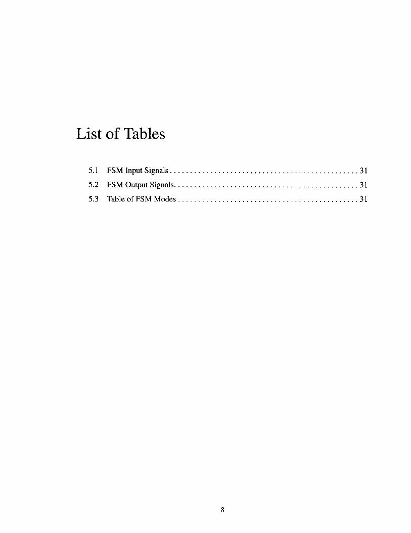
List of Tables
5.1 FSM InputSignals...............................................31
5.2 FSM Output Signals..............................................31
5.3 Table of FSM M odes.............................................31
8

Chapter 1
Overview
The new lab project, which is intended to replace the second lab in 6.111, is the
design of a coin operated vending machine controller. The vending machine controller is
an interesting and familiar subject for students which also provides practical experience in
the design of a digital system. Central to this design process is the use of a high level
description language, VHDL, to implement and debug certain hardware components of
the lab. By teaching VHDL, this lab gives students a very valuable and powerful tool
which is used in industry today.
This assignment requires students to implement a Finite State Machine (FSM) to
determine the behavior of the vending machine controller.The system takes as inputs vari-
ous control signals and switches as well as coin inputs. Based on these signals, the con-
troller will step through the different states of the FSM and provide outputs as described
by FSM's state transition table. A vending machine controller was chosen because it is a
very common piece of equipment all students are familiar with. By eliminating the confu-
sion of describing a complex user interface, this project allows students to focus purely on
the design.
9
This document describes the design and implementation of the lab. It begins with
a discussion concerning why a new lab is needed as well as various issues involved in
designing this lab. It will then describe the actual design process through which the lab
assignment was produced and various problems and changes that resulted from imple-
menting the lab. The lab handout given to the students, a sample solution, as well as
checkoff guidelines for the lab are included in the next sections. The conclusion sums up
the work that has been done and evaluates the effectiveness of this project.
10

Chapter 2
Background
This chapter describes the background behind the design of a new Lab Two for
6.111. Understanding the background is important because it gives a sense of purpose for
the project. It is also important to know how this project fits with the rest of the work that
has been done. Finally, clearly defined goals for the new lab will help focus the design
and implementation of this project.
2.1 Updating 6.111
College courses have an inherent problem of not staying up to speed with current
technology. 6.111 is no exception. Digital technology has become so complex that indus-
try designers need to use a high level language to describe these circuits. Until a couple of
years ago, 6.111 did not have that capability. A very strong effort has been made to cor-
rect this problem by adopting VHDL as part of the curriculum. This thesis is another step
toward making 6.111 a more useful class for students.
11
............
2.1.1 Previous Work
Marc Tanner '98, as a graduate student at MIT under the supervision of Prof.
Troxel first investigated the use of VHDL in 6.111 [1]. He established the infrastructure
for using VHDL and researched what hardware and software should be used in order to
make programming Complex Programmable Logic Devices (CPLDs) with VHDL a viable
option for the students. To demonstrate these new tools Marc implemented a new design
for the third lab of 6.111.
2.1.2 Work Since
Since Marc's update, some changes to the other two labs have been made. In the
fall term of 1998, the students were given the option to implement the second lab using
VHDL [2]. They had the choice of designing the project with the old tools, using a CPLD
chip to implement the FSM only, or implementing the entire lab using one or two CPLDs.
Lab One has also been updated to introduce students to VHDL programming [3].
2.2 Problem Statement
As a continuation of the work that has been done, identifying the specific problems
that remain is an important step. There are three issues that serve as the impetus for
designing a new lab. The first one is to add an increased emphasis on testing and verifica-
tion. The second is to add more flexibility to the class. Third is to bridge the gap between
the updated Lab Three with the rest of the curriculum.
12
9'" , 001

2.2.1 Testing and Verification
Testing has become a vital part of the digital design industry. Because microelec-
tronic devices have become increasingly complex, testing has become an immense prob-
lem. In 6.111, verifying the functionality of a completed system is all that has been done
in the past. This, however, is not enough. Testing systems beyond base functionality is
essential in developing a robust, cost effective product. Designers seek to investigate and
solve as many unanticipated problems as possible before the product reaches the market.
Because testing is very important in industry, it is worthwhile to investigate adding this
aspect to the class.
2.2.2 Flexibility
For many years, the lab exercises for 6.111 have remained relatively unchanged.
Although the specifics of the projects had been altered to prevent students from copying
previous work, the actual project topics have not changed. The design methodology that is
taught in lab still remains valid, but the students would benefit from the design of a new
lab. The new up-to-date lab will not only help to increase student interest, but also add
flexibility to the 6.111 curriculum by providing the instructors with more choices of lab
projects.
2.2.3 Bridge for Lab Three
This lab serves as a bridge between Lab One and Lab Three. After Marc Tanner's
successful update of the third lab, students have been learning how to use VHDL effec-
tively. However, lab three has traditionally been a very large and time consuming project.
13

Having to learn how to use a completely new language to implement their projects is a lot
to ask from the students. The work to upgrade the old Lab Two was an effort to make a
smoother transition. Because the lab was not designed to teach VHDL, it was only par-
tially successful. A new lab focusing on teaching the basics of VHDL programming, is
necessary to make the curriculum more rewarding for the students.
2.3 Design Goals
The lab assignment must satisfy certain design criteria before it can effectively
address the problems stated above. Traditionally, the second lab is the first exposure 6.111
students have to the design process. Therefore, the assignment must emphasize that pro-
cess. This means the project must not be too complex. Otherwise, it will distract from the
educational goals of the lab.
2.3.1 Educational Goals
The new lab must augment the old educational goals with the new tools that have
been made available to the students. FSM control, memory usage, and timing circuitry are
all concepts that have been taught in the past. For this lab, the students are asked to imple-
ment some of these components using VHDL.
The assignment must present the students with the necessary steps to properly
design and build a digital system. This presentation, however, cannot be too restrictive,
limiting the students' creativity in coming up with their own design. Also, testing and ver-
14
w.- _*A,

ification must be added to these steps because these concepts are vital components of
proper design.
2.3.2 Scope of Project
As a continuation of prior work, this lab must utilize the new tools and hardware
that has been incorporated into 6.111. VHDL and CPLDs should be used in the design of
the project. The project must also be a practical application of digital design students can
relate with. To make the lab a rewarding educational experience, the project itself must be
challenging and interesting for the students.
The new lab must be completed within the time allotted. With an increase in com-
plexity and the addition of a testing and verification strategy, the scope of the project has
the potential to become too large. Therefore, when designing the lab it is important to set
reasonable goals the students can accomplish in time.
15

Chapter 3
Design of the Laboratory Assignment
A Coin Operated Vending Machine Controller offers an ideal choice for the second
lab in 6.111. The controller is simple enough to be implemented using a simple FSM,
while being complex enough to make an interesting design project. It offers a wide range
of possibilities for the actual representation of the vending machine as well as the structure
needed to teach concepts of digital design. All of the students should be familiar with
examples of this product making it a fun project for them to build and demonstrate.
This chapter describes how a vending machine controller design was adapted to fit
within the constraints of a 6.111 lab. The first section discusses how the control of a vend-
ing machine is possible using an FSM. The second section addressed organization of the
lab assignment. The last section discusses how this assignment satisfies the design crite-
ria.
3.1 Vending Machine Operation
16

Although a vending machine is a very complex piece of machinery, the electronic
controls are rather simple. FSM control of the vending machine is possible because the
physical actions of the machine can be broken down to a small number of distinct states.
These states are enumerated within the FSM and control is achieved by encoding the
appropriate state transition table [4].
For this assignment, the model of the vending machine can be broken down into
four modes: program, display, vend, and test. The action the vending machine will take in
each mode is determined by a sequence of steps, each represented by a state. There are a
few other states which govern the flow of the table as well as some initial start-up states. It
is a conglomeration of all these states that the FSM is built.
3.2 Organizing the Assignment
The laboratory assignment which is handed out to students at the beginning of the
lab is included in chapter 4. The purpose of the handout is to give students information
about the project they are about to undertake. It outlines the specifications of the vending
machine, presents a suggested solution, and states the various deadlines for the lab. Also,
it clearly outlines the steps the students need to follow in order to design their project. The
project itself is divided into three sections: design review, implementation, and report.
3.2.1 Design Review
Because this is the first design problem many of the students will encounter, it is
necessary to help them throughout this process. The design review offers the students an
17

opportunity to discuss their design with the instructors. It also gives the instructors an
opportunity to check and evaluate the students' progress.
Before the review, students are required to design and draw block and circuit dia-
grams for most of their components. They are encouraged to take a look at various timing
issues for each of the components and understand how that would affect their design.
Also, they should have a state transition diagram describing the behavior of the vending
machine controller.
During the design review, the students will go over their design with a TA. The TA
will correct any errors in the design, offer suggestions to make the design better, and
answer any questions the students might have about the design. Only after talking with a
TA will they be able to continue with their lab.
3.2.2 Building the Project
After the design review, students have two weeks to build and demonstrate their
controller. During this time, they need to wire up the hardware on their lab kits, write the
VHDL code that will be programmed into the CPLD, and debug their project. During the
demonstration, the TA's will have a set of guidelines which will help facilitate this check-
off process. These guidelines are included in chapter 7.
3.2.3 Laboratory Report
The final task the students are required to complete is a written report of the lab.
The content of this report should include a section on the specifications of the vending
machine controller and a description of the controller they implemented. The students are
18
W-M..

to include circuit, block, and timing diagrams for the various components of the project.
Also, any VHDL code they programmed should be attached to this document.
The required report is intended to be a clear and concise description of their work.
The students have the option of submitting this document to MIT's writing department to
fulfill their phase two writing requirement. If they choose to do so, there are more guide-
lines for both content and format the students will need to follow.
3.3 Satisfying Design Criteria
This project satisfies the design requirements as stated in chapter 2.
3.3.1 Educational Goals
The educational goals for this lab are to teach various digital design theories using
the up-to-date tools available to the students. This lab requires the students to use an FSM,
memory unit, and clock generator in the implementation of their design. The students are
also required to use VHDL in designing and realizing their FSM component. The experi-
ence the students gain is not just an understanding of the usage of these components and
the structure of the VHDL programming language; they also gain practical experience
using these design tools.
This lab also presents the design process clearly and succinctly. The handout gives
students specific steps in the design and implementation of their project. For the third lab,
they design another, more complex project. By the end of the two labs, the students
19

should be confident enough with their design skills to be able to conceive, design and
implement their final project.
3.3.2 Scope of Project
Because this lab is centered around a VHDL implementation of the FSM control-
ler, students will gain experience using these tools. Also, the vending machine controller
is a very practical electronic component. Digital designers in industry could conceivably
work on a similar problem.
This familiar subject of the project is both challenging and interesting. It is also
small enough for the students to build in lab. Because the controller is relatively simple,
the time involved in building it should fall within the constraints of the class.
20

Chapter 4
A Discussion on Implementation.
This chapter discusses how well this lab assignment was implemented. There
were some initial problems that caused difficulties for the students. Based on feedback
received from the students, changes were made to improve the lab. There is, however,
more work that can be done to make the lab even better.
4.1 Initial problems
Despite the fact that the lab assignment was designed to make the learning experi-
ence challenging but fun, there were some problems with the lab that made it a frustrating
experience for the students. These problems detracted from the educational value of the
exercise.
4.1.1 Fitting
The problem that plagued the students the most was fitting their VHDL code in the
CPLD provided. Although there is enough of space on the chip, the students had difficulty
21

making their project fit. The main cause of this problem was that students did not have
enough experience with VHDL. Their code was inefficient because they did not under-
stand how it synthesizes into hardware. Also, they did not know how to solve the fitting
problems themselves.
4.1.2 Testing
Students traditionally approached testing as an afterthought. They like to design
things and tend to ignore testing beyond basic functionality. Unfortunately for this lab,
testing became more of a chore rather than an integral component of the design. Because
students left testing toward the end, some never completed it. Also, the testing routines
took up a large amount of space in the CPLD, adding to the fitting problem. Many stu-
dents resented having to implement testing without understanding the necessity of proper
testing in industry.
4.2 Student Feedback
Students were given the opportunity to comment on the content and implementa-
tion of this lab. Approximately 15 out of 88 students responded to an informal e-mail sur-
vey that was sent the class mailing list. Other students talked with TAs and LAs in lab,
some included a feedback section in their report. The students predominantly felt that this
lab was very frustrating and difficult. They cited several reason that contributed to this
opinion.
22

4.2.1 Software vs. Hardware
The heart of this lab is the code that is programmed into the CPLD. Students only
needed to wire three chips. Feedback from the students indicated that they felt most of
their time was spent coding rather than designing hardware. They felt that they were so
occupied with debugging their code that they did not learn digital design skills.
4.2.2 Learning VHDL
Although most of the students' time was spent coding, the feedback indicated that
the students did not feel they understood VHDL. They felt that the fitting issue was such a
distraction that they did not have time to learn proper VHDL programming.
4.2.3 Difficulty Compared to Lab Three
One of the initial goals of this lab was to facilitate the learning of VHDL in order
to make the transition to lab three smoother. Conversations with the students after they
finished the third lab indicated that the experience with VHDL did make the that lab much
easier to understand. In fact, they felt the third lab was easier than the second. However,
the transition between Lab One and this lab became disjoint.
4.3 Modifications to the Lab
Using observations made in lab and feedback from both students and instructors,
several changes have been made to the lab assignment. These changes will hopefully
address some of the problems the students had.
23

4.3.1 More Structured Assignment
Teaching proper coding of VHDL will address better understanding of digital sys-
tems as well as the fitting problem. The crux of the problem is that this lab is the first time
students have to apply the knowledge imparted to them in lecture. The original assign-
ment only outlined the system level diagram without detailing how the VHDL code should
be structured. This left the students with too much to figure out independently.
This is the first time students are asked to design digital hardware; it is also the first
time they are asked to code in VHDL. To facilitate learning these two concepts, a more
structured assignment is necessary. The key to understanding digital design and how
VHDL fits into the picture is to realize that VHDL is a hardware description language.
Digital engineers use VHDL to describe the hardware they design.
Conceptualizing the CPLD as discrete elements will help students learn proper
digital design and VHDL programming. Having the students think about implementing
the CPLD as separate hardware components will reinforce basic concepts of digital
design. Asking them to code each component separately will help their understanding of
VHDL code organization.
4.3.2 Testing Eliminated
Although testing is a very important part of any design process, it is too important
of a topic to be added as an afterthought. Testing and verification is such a large task that
many companies require a separate group of engineers to complete it. There is enough
material concerning testing to create an entire course at MIT. If in fact testing cannot be
24

presented properly, it is better to eliminate it rather than distract the students from learning
more central concepts.
4.4 Future work
Although the changes that have been made should make this lab more rewarding
for the students, many things that can be done to improve it.
4.4.1 Testing and Verification
As stated above, testing should not be attempted unless it is taught properly. Eval-
uating the practicality of testing in a lab is necessary before it can be implemented. If
implemented, it requires more specific instructions in the laboratory handout. The instruc-
tors and lab assistants must fully support and encourage students in this endeavor.
4.4.2 More Modifications
If this lab is used in the future, small changes are necessary to prevent students
from copying previous projects. Some easy modifications can change the user interface or
the model of the vending machine. Changing the number of coin inputs or products is rel-
atively simple.
A more involved modification is to utilize the timer circuit students build in lab
one. The timer could control a timeout signal. If the user does not select a product before
the time expires, the collected money would be returned. This signal can even be used to
25

make the outputs "cleaner." The machine will display the price, change and product
vended for a certain amount of time, after which the displays would be cleared.
4.4.3 An Interactive Demo
The current demo project consists only of a lab kit. To present this to the students,
a camera would be used to project the kit onto a screen. One of the original goals of this
project was to develop a more interactive and realistic demo. Unfortunately due to time
constraints, this goal was not accomplished. Therefore, building some kind of mini-vend-
ing machine, or programming a GUI for a workstation would make the project more
appealing to the students. This demo could be made available to the students to enhance
their demonstrations.
4.4.4 Designing a New Lab
This lab is closely based on the old Massachusetts Stoplight Controller Lab [2].
Because of this, the structure and implementation of the labs are very similar. It would be
worthwhile to investigate implementing a completely new type of lab. The new lab would
be able to take advantage of the many new programmable chips and boards that are cur-
rently being integrated into the class.
26

Chapter 5
The Laboratory Handout
The following section contains the laboratory assignment that was handed to the
students. It was adapted from the Massachusetts Stoplight Controller lab handout which
was used in previous semesters of 6.111 [2].
27
Massachusetts Institute of TechnologyDepartment of Electrical Engineering and Computer Science
6.111 - Introductory Digital Systems Laboratory
Laboratory 2 - Finite State Machines
Handout Date: February 17, 1999Design Due: February 24, 1999
Lab Checkoff Date: March 8, 1999Report Due: March 10, 1999
Introduction
This laboratory exercise concerns the design and implementation of a coin operated vend-ing machine controller. The heart of your implementation will be a synchronous finitestate machine (FSM).
This lab is designed to give you a methodology for designing and building a digital systemand creating procedures to test it for completeness. This lab is also designed to give youpractical experience using VHDL to implement your design.
This laboratory is an exercise that reflects current issues digital designers face in industry.Design and implementation have always been part of this industry, but as microchips havebecome more complicated and the overhead for fixing mistakes become more expensive,verification and testing has become an integral part of digital design. This lab will intro-duce some testing techniques and procedures designers use today.
Your vending machine controller FSM is also given the task of loading static RAM loca-tions with the cost of the vended products. The FSM will also display these values byreading the RAM locations.
Vending Machine Controller
The vending machine to be controlled accepts only coins (nickels, dimes, and quarters)and vends four products. There are two input switches which serve as the function andproduct selectors. There are also two reset switches.
Along with the three coin denominations, there will be another input, the execute or "GO"button. Essentially, this button will be used as the action button. In any operating mode,this is the button that will initiate any action in the FSM controller.
28

Input Switches - -
Coin Inputs Vending - - Products
GO M -- -CostMachine ost
Controller MnyILocal Reset----l
Global Reset-
Figure 5.1: Vending Machine Top Level Controller Block Diagram
As outputs, the vending machine controller should indicate to the user whether or not theproduct selected has been vended as well as the change returned. The machine should alsodisplay how much money was put in as well as how much a product costs.
Upon start-up, the user will use the global reset switch to initialize the FSM. This switchwill set off a simple routine which will test and clear the memory. If this routine fails, itwill halt the FSM. Leds will be used to indicate whether or not the start-up routine hascompleted successfully or not. The user should be able to use this switch at any time dur-ing the operation of the machine.
After running through the initial start-up routine, the operator can switch the controllerbetween four modes: normal operation, programming, display, and free. Using the selec-tion switches, the operator of the vending machine can switch between these modes byselecting the appropriate function and pressing the "GO" button.
In normal mode, the vending machine operates just like any other vending machine. Thecontroller will keep a running total when coins are deposited. To vend a product, the userwill select the product and push the "GO" button. If there is enough money in themachine, it will vend the specified product and return any change. The controller willignore any vend requests if not enough money had been deposited.
In programming mode, the prices for the products are stored in memory. Using the samebuttons used to simulate coin input, the operator of the vending machine has the ability toprogram different prices for the various products.
In display mode, the operator can display prices that were programmed into the vendingmachine controller by selecting the product and pressing the "GO" button. This will allowthe operator of the vending machine to manually check the prices that were programmed.
In free mode, the vending machine will ignore any of the programmed prices and alwaysvend a product when it is selected.
29
-- w-hange

SO
Si
GOH
Local Reset-jH
Global Reset-H
Nickel--I
Dime-
Quarter--
L
FSM+5
, -- Change
-- VendedProducts
0~4/$- - Accumulated
CLR IMoneyAw CLK
W + AccumulatorClock Generator
..... .2: - - - - - - J
Figure 5.2: System Level Block Diagram
The local reset signal is used to switch out of a mode. The operator of the vendingmachine can terminate any mode by using this switch. When this switch is activated, theFSM will return to the function selection state. From there, the operator can select thenext function to be executed. This switch should be synchronized to the system clock.
Specifications
A system level block diagram of the vending machine controller is shown in figure 5.2.There are three main components to this system, the SRAM, Clock Generator and theFSM Controller (represented by the dashed box).
The SRAM is used to store the prices for the four vended products. Remember to wire theunused RAM address lines to GND. However, leave the unused 1/0 pins unconnected.The RAM is implemented using the 6264 SRAM. Timing specification and data sheetsare included at the end of this handout.
The Clock Generator is the component that produces the FSM clock, CLK. This is thesignal that the entire system will be driven and synchronized to. You are welcome to usethe timer you constructed in Lab One.
30
A0
Al SRAM
(WE
/OE
Fost /CE CE
C No

Global RESET (from Synchronizer)Local RESET (from Synchronizer)GO (from Synchronizer)Si and SO Determine Function and Product (from switches)Accumulated Money Amount of money in the machine (from Accumulator)
Table 5.1: FSM Input Signals
Al and AO Specifies an address in the SRAMWE Drives values into SRAMOE Drives values from SRAMCost Used to read and store the cost of products to SRAMVended Products Vended product indicators (to Led's)Change Change indicator (to HEX led's)
Table 5.2: FSM Output Signals
FO F10 0 Examine memory locations specified by address switches (display)0 1 Store new value in memory location of address switches (programming)1 0 Run vending machine (normal)1 1 Vend products for free (free)
Table 5.3: Table of FSM Modes
The FSM Controller is the heart of the system. It should be implemented using VHDLand programmed into a CPLD chip. It consists of three separate components, the Syn-chronizer, Accumulator, and FSM.
The Synchronizer is used to sync the GO, coin, and reset inputs to the system clock.While it is possible to effect this synchronization by being clever and absorbing the syn-chronizing function within your FSM, it is strongly suggested that you explicitly synchro-nize the input signals with D
flip-flops. It is up to you to design the exact timing of each of these signals. Rememberthat you only want to assert any one of these signals only once per clock cycle. Also, youshould consider what would happen if multiple buttons were pushed at once.
The Accumulator is used to store the amount of money that has been put into the machine.It is up to you to devise an appropriate data representation for the money. Don't forget toinclude a clear signal which will set the value in the accumulator to 0. Also remember tooutput the accumulated money to the FSM and HEX led's.
31

The FSM itself should be the physical embodiment of the state transition table for theFSM you created. Although the Warp synthesizer takes care of creating this table, it isimportant to remember FSM timing considerations when writing the VHDL code for it.
The input and output signals for the FSM are listed and described in table 5.1 and 5.2.You may use any polarity you like, e.g., NWE or WE as you choose. table 5.3 describesthe four functions specified by the two function switches.
A partially completed VHDL source file is located in the 6.111 locker, /mit/6. 11 1/vhdl/lab2/lab2.vhd. Copy it to your locker by executing:
cdmkdir lab2; cd lab2cp /mit/6. 11 1/vhdl/lab2/lab2.vhd lab2.vhdchmod 600 lab2.vhd
The VHDL source file provided is not complete enough to create a CPLD file yet. Forexample, it does not include the complete FSM specification.
Procedure
For the sake of simplicity, use the switches and lights available to simulate the machine.The four push-buttons should be used for the three coin inputs and the GO button. Use theswitches to implement the two reset and input switches. You should use the hex leds todisplay the amount of money in the machine, the cost of the products and the changereturned, and one led per product to indicate if it has been vended.
Use the following steps to facilitate your design, implementation, test, and report of thelab.
1. Before proceeding with the details of the FSM design, you should design the circuitryneeded to synchronize the GO, Nickel, Dime and Quarter signals. You will want thesesynchronized signals to be asserted only once per clock cycle.
2. Draw up a complete logic diagram of the system and a state transition diagram of yourFSM.
3. Sketch out timing diagrams which completely demonstrate the operation of each func-tion of your FSM.
4. You should discuss the design with a member of the teaching staff before program-ming your CPLD. Bring the sketches and drawings of your FSM to this DesignCheckoff.
5. Before wiring the entire system together, it is recommended that you wire and verifyeach individual component separately. Test the functionality of the SRAM first. Use
32

the switches to manually store values into the SRAM and verify them by loading themto the led's.
6. It is recommended that you also program and verify the FSM controller in parts. Foreach separate component, use a combination of the Nova simulator, logic analyzer andmanual inputs to verify that they work. Build each component on top of each other,starting with the synchronizer, then accumulator, and finally the FSM itself.
7. Once the FSM controller has been verified, put the entire system together. Now thatyou understand how the signals work for each component, it will be easier for you todebug the interactions between the components within FSM controller as well as theSRAM. Again, use the logic analyzer to debug the various control signal outputs ofthe FSM.
8. Once you have debugged the system for functionality, you should demonstrate the sys-tem to one of the instructors. Have all your timing diagrams, state diagrams, VHDLfile, and logic diagrams available for this demonstration.
9. If you have time, you should test the system for erroneous inputs: inputs that theproject was not designed to handle. What happens when you switch into programmode during the vend cycle? What happens when you push two coin buttons at once?Investigate how robust your design is in regard to these inputs.
Laboratory Report
You should write up a report for this lab which meets the requirements specified in the"Report Guide" handout. Your report should include the following: data paths, an FSM,VHDL source file and the corresponding state diagram, at least one logic diagram, and alltiming diagrams. You should also discuss your design, method of implementing it, andhow you tested for functionality and bugs. The report should flow, be well organized, andmost importantly, be complete. Verbosity is not a requirement.
Design Tips
There are two major problems you will encounter when designing and implementing sys-tems in VHDL: understanding how the code synthesizes into hardware and fitting theentire system onto one chip. An understanding of the first will help to solve the second.These are some tips to help you solve these problems with regard to this lab as well asgeneral tips for designing digital systems.
It is very important to remember the proper approach to programming in VHDL. VHDLis a (H)ardware (D)escription (L)anguage. Instead of laying out circuits and componentsusing a CAD program or wiring various chips together, you will be describing actual phys-ical components using programming constructs.
33

Therefore, you should approach programming in VHDL like you would if you weredesigning this lab using the IC chips you have on hand. The FSM controller is separatedinto three separate parts. Think about and implement each component separately. Onceyou do, then put them together either by instantiating them using component declarationsor by declaring separate processes for each. If needed, break each of the separate compo-nents down even further. Remember that the hierarchical nature of VHDL is a very pow-erful tool.
You have been introduced in lectures and problem sets to various ways if implementingFSM's in VHDL. Because each implementation synthesizes differently, it is very impor-tant to understand how they are synthesized and the hardware that results. When design-ing your FSM think about how you would generate the equations for the outputs of yourstate transition diagram.
You will be spending a large part of your time trying to make your code fit in the CPLD.The secret to understanding how to make your VHDL code efficient is to understand howit synthesizes into hardware. As mentioned above, each different implementation of anFSM will synthesize differently. Some will take up more space than others.
Remember, you want to minimize the amount of product terms your code will generate.Think about where these product terms come from. How does changing the number ofinputs and outputs affect this? How does the number of case statements affect the numberof product terms? It is very bad to have conditionals which use comparators or arithmeticoperators. Think about how checking for one of these conditions affects the conditionalsthat don't use these operators.
It is important to realize how important PROPER verification and testing is in the designprocess. It can make the difference between success and failure. The underlying trait thatis most useful is patience. It is very easy to become so eager to program and wire up theentire system and hope that it works the first time you turn it on. Unfortunately, 99 percentof the time, it doesn't. By then, it become very hard to isolate bugs in such a complex sys-tem.
Therefore, you should have the patience to test each part of the system individually. Notonly verify that it works, but understand the timing involved in making it work. If you dothis, you will be able to eliminate the parts individually from consideration when youencounter bugs while integrating the system. You can concentrate on the interactions ofthe parts rather than the parts themselves.
The last and simplest thing you can do to make your life easier is to have the patience towire NEATLY. Instead of connecting wires using big arches, try using right angles to wirearound the chips and protoboard. Making your chips accessible is very important. Youshould minimize the possibility of unplugging a wire when you need to replace chips.Also, use different colored wires to differentiate between different lines. It is much easierto follow a single wire if its different than the wires next to it. Remember, the neater the
34

wiring, the easier it is for you, the TA's and LA's to debug your kit. The easier it is for youto debug, the more time you will save.
6264 SRAM Chip
Because you will be using a separate SRAM chip, data sheets for the 6264 SRAM areattached. PLEASE read the data sheet carefully as this chip is easily damaged by incor-rect use (wiring). ASK QUESTIONS IF YOU ARE NOT SURE!
The 6264 has a tristate Input/Output (1/0) bus. Reread the handout "Gates, Symbols, andBusses" which pertains to bussing. The 1/0 bus of the 6264 MUST be driven by a tristatebuffer; use the 74LS244 included in your kit, or you can use outputs of the CPLD.
Tristate bus contention occurs when two (or more) drivers are active at the same time. The6264 tristate output is enabled when the /OE input is asserted low, the /CS is asserted low,and the /WE line is high. While it is true that many logic designers allow tristate bus con-tention to occur for short times (due to chip delays), it is not a good idea. For this labora-tory exercise you are to ensure that NO tristate bus contention can occur.
/CS tied to /WE /CS tied to CLK
CLK CLK
/CS /CS
AVE /WEI
ADDR valid ADDR v id
start write start write
Figure 5.3: SRAM Address Timing
The actual write pulse is the AND of both the /CS and the /WE asserted low. It is essentialthat the address lines to the SRAM not change when the write pulse is active. Otherwiseyou may write to multiple locations!
While the 6264 is advertised as a static RAM, a memory cycle is actually initiated when-ever ANY address line changes. Thus, the address lines may NOT be tristated wheneverthe /CS is asserted, as the internal timing circuitry is actuated by noise on the HI-Z addresslines.
One way to solve both the tristate bus contention and address holding problems is to con-nect /CS to the CLK signal. This fix prevents bus contention because the SRAM does notdrive the output when /WE is asserted low before /CS is asserted. Figure 3 outlines thereason this fix solves the address holding problem. The left diagram has /CS ties to /WE.We see that the address isn't valid when the write occurs. The right diagram shows /CS
35

tied to CLK. It is obvious to see that the address have enough time to settle before thewrite happens.
More specific timing diagrams for both the read and write cycle for the SRAM areincluded with the data sheets.
36

Chapter 6
A Sample Solution
This chapter describes a sample solution to the Vending Machine Controller
assignment. Built to satisfy the specifications set in the Laboratory Handout, this solution
can be used as a demonstration for the students. It is only one of many possible solu-
tions.
Following the design recommendations in the Lab Handout, the Coin Operated
Vending Machine Controller can be split up into three hardware components: the CPLD,
memory storage unit, and clock generator. There are three components programmed into
the CPLD: the synchronizer, accumulator, and FSM. Figure 4.2 on page 28 shows the
system level diagram, and the VHDL code for this project is included in Appendix B.
6.1 Clock Generator
The clock signal is generated using a 1.8432MHz square wave crystal oscillator.
Although the frequency of the oscillator is slow enough to handle the propagation delays
of the system, the clock signal is used to drive a divider circuit because the oscillator has a
low fanout. All that is required is to feed the clock signal through a buffer. However, the
37

Figure 6.1: Clock Generator Schematic
students should have already built a clock timer circuit in the first lab and have the option
of using it. This example does use a timer circuit. The divider is built out of three four bit
counters (74LS393) [5]. By taking the 11th bit of the counter chain, a 450Hz clock signal
is generated.
6.2 Memory Storage Unit
This project uses a 6116 SRAM to implement the memory storage unit. Although
the handout given to the students recommends using a 6264 SRAM, the 6116 SRAM
behaves almost identically to the 6264 SRAM. The only perceivable difference is that the
6116 SRAM doesn't have the extra chip select pin. Because this pin is tied to Vdd when
the 6264 SRAM is used, its absence in the 6116 SRAM is inconsequential. The pin
assignments for the SRAM are shown in Figure 6.2.
6.3 CPLD
A 372i CPLD is used to store the VHDL implementation for the three programmed
components [6]. The CPLD also has the capability of storing up to 320 product terms,
divided up into 64 macrocells. 32 macrocells are used for 1/0, the remaining 32 are buried
within the chip. The CPLD has a total of 37 possible external pin connections. These
38

Figure 6.2: CPDL and SRAM Schematic
specifications are sufficient to implement the three components programmed in the CPLD.
This example only uses 34 pins, 50 macrocells, and 259 product terms.
The CPLD takes as inputs the clock, coin inputs, go, local and global reset, and
address switches. It outputs to the SRAM the address, write enable, and output enable sig-
nals. Price, change, and accum go to the hex leds and the product selection indicators go
to the normal leds. Figure 6.2 shows the pinout assignments of the CPLD.
As seen in figure 5.2, the functionality of the CPLD can be split into three distinct
components: the synchronizer, accumulator, and the FSM. This project separates these
components into three different files, with synchronizer and accumulator instantiated
within the top-level FSM file. The reasons these components are separated are to take
advantage of VHDL's hierarchical organizational capability, to allow for flexibility in the
system's design, and to facilitate testing and debugging [7].
39
SInu- D Q - D Q D Q OutputgQ1 Q2 Q3
CLK
CLK
Input
Q1
Q2
Q3
Output
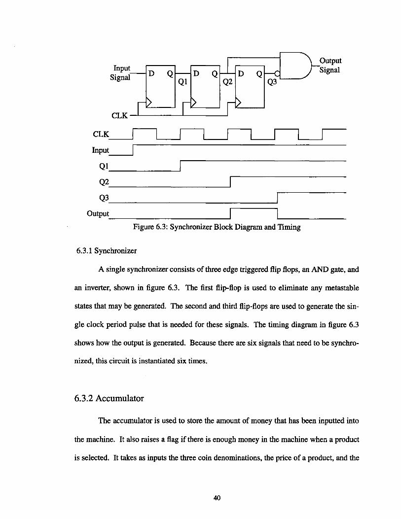
Figure 6.3: Synchronizer Block Diagram and Timing
6.3.1 Synchronizer
A single synchronizer consists of three edge triggered flip flops, an AND gate, and
an inverter, shown in figure 6.3. The first flip-flop is used to eliminate any metastable
states that may be generated. The second and third flip-flops are used to generate the sin-
gle clock period pulse that is needed for these signals. The timing diagram in figure 6.3
shows how the output is generated. Because there are six signals that need to be synchro-
nized, this circuit is instantiated six times.
6.3.2 Accumulator
The accumulator is used to store the amount of money that has been inputted into
the machine. It also raises a flag if there is enough money in the machine when a product
is selected. It takes as inputs the three coin denominations, the price of a product, and the
40

Figure 6.4: Accumulator Block Diagram
accumulator clear signal. It outputs the accumulated money and a status signal which
indicates that there is enough money in the machine.
Money is stored as the denomination of the coin divided by 5 (nickel = 1, dime =2,
quarter = 5). When a coin is deposited, the accumulator will add that amount of money to
the running total. Also, it always checks the running total against the price of the product.
If it is greater than the price, then the "enough" flag is raised. Finally, when the accumula-
tor clear signal is set to 1, the accumulator will clear the accumulated money.
The VHDL code for the accumulator is separated into two processes indicated by
the dashed boxed in figure 6.4. The first is a clocked process which contains the code that
accumulates the money. The second process contains the comparator which determines
whether or not to raise the enough flag. It is implemented as combinational logic.
6.3.3 FSM
The FSM is implemented according to the specifications described in the lab hand-
out. This design uses a 11 state mealy machine to implement its functionality. The FSM
41
11% .......... .....

All transitions except for globalreset states, comp and clearoccur on go = 1.
On global reset from any state,next state = globall.
Program, Display and Free willperform their programmedactions when go is pressedand loop back to themselves.
Figure 6.5: FSM State Transition Diagram
will determine the outputs and next state based on the current state and inputs. Figure 6.5
shows the state transition diagram of the FSM.
The VHDL code for the FSM is split into two different processes. One process
takes the current state and the inputs and determines the next state and output. Essentially,
this is the process which encodes the state transition table for the FSM. The other process,
clocks the next state into the current state. This clocked process regulates the states.
Upon start-up and global reset, the controller will start the global reset routine.
This sequence of four states will clear the contents of the SRAM. The controller will then
42

transition to the idle state. When the go button is pushed in the idle state, the controller
will select one of the four states to go to based on switch inputs.
If go is pressed in the program mode, the controller will set the address to the
switch inputs, the SRAM input to the accumulated price, and the SRAM to write. The
price that was set will be programmed to the appropriate address in memory.
If go is pressed in the display mode, the controller will set the address to the switch
inputs and the SRAM to output the data. Because the output is already connected to the
hex leds, the cost of the product will be displayed.
In vend mode, the controller will transition to the comp state only if the cost of the
product is less than or equal to the accumulated money. Otherwise it will remain in the
vend state. If there is enough money, the controller will output the calculated change and
appropriate led indicator. It will then transition to the clear state where the accumulator is
cleared.
In free mode, the controller will ignore all accumulated money and cost of prod-
ucts. When go is pressed, it will light up the appropriate product leds based on the input
switches.
In all four modes, if local reset is selected, the modes will transition to the idle
state. Also, if the global reset is selected in any of the states, the machine will immedi-
ately transition to the first global reset state.
43

Chapter 7
Checkoff Guidelines
This chapter contains the guidelines TAs can use to help checkoff students' lab
projects. It is important to remember that these are only guidelines. It is up to the TA's
judgment whether or not the students have satisfied the lab requirements. If they can jus-
tify their design choices, then their project is satisfactory.
44

Lab 2: Vending Machine ControllerCheckoff Guidelines
Basic Functionality
The hardware components are the first thing to check. Check the wiring for the clock gen-erator, SRAM, and CPLD. Pay attention especially to how the SRAM is wired up. Askthe students how any why they wired up the SRAM.
When checking off the CPLD, ask the students to produce their VHDL code. Make surehe/she understands how the code relates to the operation of the machine. Ask them howtheir code would be synthesized into hardware components. If convenient, have the stu-dents show a simulation of the components. If they did not use the simulator, encouragethem to do so for the next lab.
Next, ask them how they implemented the synchronizer and accumulator. Make sure theyunderstand why the synchronizer needs three flip flops instead of two. Also ask about howthe delayed synchronizer output affects the operation of the FSM. For the accumulatorcheck to see that the code does indeed works. Point out places where code might be inef-ficient.
To verify the base functionality of the FSM, have the students demonstrate that each of thefour functions of the vending machine controller works. Have a copy of their state transi-tion diagram handy. Ask the students to step through the diagram while demonstratingtheir project.
The programming and display modes can be verified in conjunction. Have the studentsprogram distinct prices in each of the four products. Verify that the correct price was pro-grammed using the display mode.
To verify the vend mode, use the prices programmed when verifying the programmingmode. Try different combinations of coin inputs to verify that the accumulator is working.Vending products with accumulated money that is greater than, equal to, and less than theprice of a product. Make sure that the correct price, change, and product light are dis-played when the product is vended. The product led should not light up if not enoughmoney was inputted.
The local reset signal should be functional, otherwise switching between modes would notbe possible. One thing to make sure, on local reset, the accumulator should be cleared.For the global reset signal, verify that all the memory locations are cleared using the dis-play mode.
45

Questions to Ask Students
These are interesting issues that the students are not required to have an answer for. Ifthey have not addressed them, then bringing it up is sufficient. If they have addressedthese issues in their design, they should be rewarded appropriately.
1. What happens when the accumulator rolls over? What is a good solu-tion to this problem?
2. What will happen if multiple inputs are pressed at once? Will all theinputs be processed? If not, which input has precedence?
3. What state does the machine start when it is first powered up? Whatwould happen if somehow the machine got stuck in an unanticipatedstate?
4. How is their VHDL code organized and why did they choose to orga-nize it in that manner? Why does separating the components make thedesign process easier?
5. What part of the VHDL code takes up the most space in the CPLD?Why?
46

Chapter 8
Conclusion
This new lab for 6.111, The Coin Operated Vending Machine Controller, succeeds
as a continuation of the work that has been done to update the 6.111 curriculum. It effec-
tively utilizes the new tools that were recently developed while leaving room for future
technological improvements.
It offers a solution to the problems stated in Chapter 2 while staying within the
confines of the design goals. Designed with VHDL in mind, this lab takes advantage of
the power inherent in designing digital systems using a high level description language. It
accomplishes this without adding more complexity to the problem. Students are given a
clear and concise learning experience.
Some problems did occur with the initial implementation of the lab. However,
these problems were minor, only distracting minimally from the educational purpose of
the lab. With the understanding and patience of the students and the support of the teach-
ing staff, an improved lab is the result of this endeavor.
Although there is still more work that can be done to make this lab even better, this
lab can stand in its current form. It does serve a very useful and educational purpose. The
47

success of the students even through the initial problems is a testament to that fact. The
reactions from students were positive and the staff does intend to use the new lab for
future classes. Except for the failure to integrate testing into the curriculum, the imple-
mentation of this new lab can be deemed as a success.
48

Appendix A
Listing of Code Provided to Students
This appendix contains the files which were provided to the students. The code
only gives a framework in which the students were to work.
A. 1 Example FSM: lab2.vhd
-- This lines are the library and use clausesLIBRARY ieee;USE ieee.stdjlogic_1164.ALL;USE work.stdarith.all;
-- This is the FSM's entity declaration.-- Note that it is not complete.ENTITY fsm IS
PORT (clk, go: IN stdjlogic;led: OUT stdlogicvector(3 downto 0));
END fsm;
-- This is the FSM's archticture declaration.ARCHITECTURE archfsm OF fsm IS
-- External component declarations go here.-- The actual entity and architecture declarations can be --
-- written in a separate file.COMPONENT sync
PORT (clk, x: IN stdjlogic;
49

y: OUT stdjlogic);END COMPONENT;
-- These lines set up the state encoding as well as any-- signals.
TYPE states IS (statel, state2);SIGNAL pstate, n-state: states;
BEGIN
-- This is how you instantiate a component.go-s: sync port map(clk => clk, x => go, y => syncgo);
-- This process encodes the FSM's state transition tablePROCESS (syncgo)BEGIN
CASE p_state ISWHEN statel => led <= "1100";
IF syncgo = '1' THENn_state <= state2;
ELSE
n_state <= statel;END IF;
WHEN state2 => led <= "0011";IF syncgo = '1' THENn_state <= statel;
ELSE
n_state <= state2;END IF;
END CASE;
END PROCESS;
-- This process creates the register the states are clockedthrough.PROCESS (clk)
BEGIN
IF risingedge(clk) THENp-state <= nstate;
END IF;
END PROCESS;
END archfsm;
50

Appendix B
Listing of Code Used in the
Sample Solution
This appendix contains listings of code used in the sample solution to the labora-
tory assignment. This code is not handed to the students. The framework for the sample
code handed to the students is generated from the overall structure of this code.
B.1 Synchronizer Code: sync.vhd
This file contains the code for the synchronizer. Signal x and clk are the inputs, y
is the synchronized output. The three flip-flops are instantiated by the clocked process.
Because the AND gate is combinational, it is instantiated outside of a process.
library ieee;USE ieee.stdjlogic_1164.ALL;
ENTITY sync isPORT (clk, x: IN stdlogic;
y: OUT stdjlogic);
51

END sync;
ARCHITECTURE pulse OF sync ISSIGNAL a,b,c: stdjlogic;
BEGIN
y <= b AND (NOT c);
PROCESS (clk, x, a, b, c)BEGIN
IF risingedge(clk) THENc <= b;
b <= a;
a <= x;
END IF;
END PROCESS;
END pulse;
B.2 Accumulator Code: accum.vhd
This file contains the code for the accumulator. It contains the two process
described in chapter 6.
LIBRARY ieee;
USE ieee.stdjlogic_1164.ALL;USE work.stdarith.all;
ENTITY count IS
PORT (clk, reset: IN stdjlogic;quarter, nickel, dime: IN stdjlogic;price: IN stdlogic-vector(3 DOWNTO 0);enough: OUT stdjlogic;accum: BUFFER stdjlogicvector(3 DOWNTO 0));
END count;
ARCHITECTURE archcount OF count IS
BEGIN
PROCESS (price, accum)BEGIN
IF accum >= price THENenough <= '1';
ELSE
enough <= '0';
52

END IF;END PROCESS;
PROCESS (clk, reset, quarter,BEGIN
IF risingedge(clk) THENIF quarter = '1' THENaccum <= accum + 5;
ELSIF nickel = '1' THENaccum <= accum + 1;
ELSIF dime = '1' THENaccum <= accum + 2;
ELSIF reset = '1' THENaccum <= "0000";
END IF;END IF;
END PROCESS;END archcount;
nickel, dime, accum)
B.3 FSM Code: vendcont.vhd
This file contains the code for the FSM. It is split up into two processes. One
encodes the state transition table. The other clocks the next state into the current state.
The synchronizer and accumulator are both instantiated in this file.
LIBRARY ieee;USE ieee.stdlogic_1164.ALL;USE work.stdarith.all;
ENTITY fsm ISPORT (clk, resetg, reset_1: IN stdjlogic;
go: IN stdjlogic;sw: IN stdjlogicvector(1 downto 0);quarter, nickel, dime: IN stdjlogic;price: INOUT stdjlogicvector(3 downto 0);we, oe: OUT stdjlogic;addr: OUT stdlogic-vector(1 downto 0);led: OUT stdlogicvector(3 downto 0);change: BUFFER stdjlogicvector (3 downto 0);accum: BUFFER stdjlogicvector(3 downto 0));
ATTRIBUTE pin-numbers OF fsm: ENTITY IS"price(0):31 price(l):30 price(2):29 price(3):28" &
53

led(O):2 led(l):3 led(2):4 led(3):5" &change(Q):27 change(l):26 change(2):25 change(3):24" &go:6 nickel:15 dime:16 quarter:17" &addr(O):39 addr(1):38 we:37 oe:36 sw(O):32 sw(1):43";
END fsm;
ARCHITECTURE archfsm OF fsm ISCOMPONENT count
PORT (clk, reset: IN stdlogic;quarter, nickel, dime: IN stdjlogic;price: IN stdlogic-vector(3 DOWNTO 0);enough: OUT stdjlogic;accum: BUFFER stdlogic-vector(3 DOWNTO 0));
END COMPONENT;
COMPONENT syncPORT (clk, x: IN stdjlogic;
y: OUT stdjlogic);END COMPONENT;
TYPE states IS (globall, global2, global3, global4, idle,program, display, vend, comp, clear, free);
SIGNAL pstate, nstate: states;SIGNAL reseta: stdlogic;SIGNAL syncreset_l, sync-reset-g, sync-go: stdlogic;
SIGNAL sync-nickel, sync_dime, syncquarter: stdjlogic;SIGNAL enough, subgo: stdlogic;
BEGIN
gos: sync port map(clk => clk, x => go, y => syncgo);reset_1_s: sync port map(clk => clk, x => reset_1,
y => syncreset_l);reset_g_s: sync port map(clk => clk, x => reset_g,
y => syncreset_g);nickels: sync port map(clk => clk, x => nickel,
y => sync-nickel);
dimes: sync port map(clk => clk, x => dime,y => sync-dime);
quarters: sync port map(clk => clk, x => quarter,y => syncquarter);
accumulator: count port map(clk => clk, reset => reseta,quarter => syncquarter, nickel => syncnickel,
dime => sync-dime, price => price,
enough => enough, accum => accum);
54

PROCESS (p-state, syncresetg, syncreset 1, syncgo, sw,enough, accum, change, price)
BEGIN
IF sync_resetg = '1' THENn_state <= globall;
ELSE
CASE pstate ISWHEN globall => price <= "0000";
we <= '0';oe <= '1';
addr <= "00";n_state <= global2;
WHEN global2 => price <= "0000";we <= '0';oe <= '1';addr <= "01";n_state <= global3;
WHEN global3 => price <= "0000";we <= '0';oe <= '1';
addr <= "10";n_state <= global4;
WHEN global4 => price <= "0000";we <= '0';oe <= '1';addr <= "11";n_state <= idle;
WHEN idle => price <= "ZZZZ";led <= "0000";
change <= "0000";we <= '1';
oe <= '1';reseta <= '0';IF syncgo = '1' AND sw = "00" THENn_state <= program;
ELSIF syncgo = '1' AND sw = "01" THENn_state <= display;
ELSIF syncgo = '1' AND sw = "10" THENn_state <= vend;
ELSIF syncgo = '1' AND sw = "11" THENn_state <= free;
ELSE
n_state <= idle;END IF;
WHEN program => oe <= '1';
IF syncreset_1 = '1' THEN
55

we <= '1';price <= "ZZZZ";reseta <= '1';n_state <= idle;
ELSIF syncgo = '1' THENaddr <= sw;we <= '0';price <= accum;reseta <= '1';n_state <= program;
ELSEprice <= "ZZZZ";we <= '1';n_state <= program;
END IF;WHEN display => we <= '1';
price <= "ZZZZ";IF syncreset_1 = '1' THEN
oe <= '1';n_state <= idle;
ELSIF syncgo = '1' THENaddr <= sw;oe <= '0';n_state <= display;
ELSEoe <= '0';n_state <= display;
END IF;WHEN vend => we <= '1';
price <= "ZZZZ";
IF sync-resetl = '1' THENoe <= '1';reseta <= '1';n_state <= idle;
ELSIF syncgo = '1' AND enough = '1' THENaddr <= sw;oe <= '0';n_state <= comp;
ELSEoe <= '1';n_state <= vend;
END IF;WHEN comp => we <= '1';
oe <= '0';price <= "ZZZZ";change <= accum - price;
56

n_state <= clear;IF sw = "00" THEN
led <= "0001";ELSIF sw = "01" THEN
led <= "0010";ELSIF sw = "10" THEN
led <= "0100";ELSE
led <= "1000";END IF;
WHEN clear => we <= '1';oe <= '1';reseta <= '1';price <= "ZZZZ";
n_state <= vend;WHEN free => we <= '1';
oe <= '1';price <= "ZZZZ";
IF sync-reset_1 = '1' THEN
n_state <= idle;ELSIF syncgo = '1' AND sw
led <= "0001";
n_state <= free;ELSIF syncgo = '1' AND sw
led <= "0010";
n_state <= free;ELSIF syncgo = '1' AND sw
led <= "0100";
n_state <= free;ELSIF syncgo = '1' AND sw
led <= "1000";
n_state <= free;ELSE
n_state <= free;END IF;
WHEN others => we <= '1';oe <= '1';price <= "ZZZZ";
n_state <= globall;
= "00" THEN
"01" THEN
"10" THEN
"11" THEN
END CASE;
END IF;
END PROCESS;
PROCESS (clk)BEGIN
IF risingedge(clk) THEN
57
,4- -- -1- - - -- z-- --- - - '-

p-state <= nstate;END IF;
END PROCESS;
END archfsm;
58

Biblography
[1] Marc D. Tanner. Helium Breath: An Updated 6.111 Curriculum. Master's Thesis,Massachusetts institute of Technology, May 1998.
[2] Donald E. Troxel. 6.111 Laboratory 2: Massachusetts Stoplight Controller. Massa-chusetts Institute of Technology. Spring 1999 edition.
[3] Donald E. Troxel. 6.111 Laboratory 1. Logic Analizers, Digital Oscilloscopes, PALs,and CPLDs. Massachusetts Institute of Technology. Spring 1999 edition.
[4] Prof Troxel and James Kirtley. 6.111 Lecture Notes. Massachusetts Institute of Tech-nology.
[5] Texan Instruments. The 7TL Data Book, 1988 edition, 1994.
[6] Cypress Semiconductor, Programmable Logic Data Book, 1996 edition, 1995.
[7] Kevin Skahill. VHDL for Programmable Logic. Addison-Wesley, Menlo Park, 1996.
59