Embed Size (px)
Citation preview
1 2 3 4 5 6 7 8 91011121314151617181920212223242526272829303132333435363738394041424344454647484950515253545556576061
1
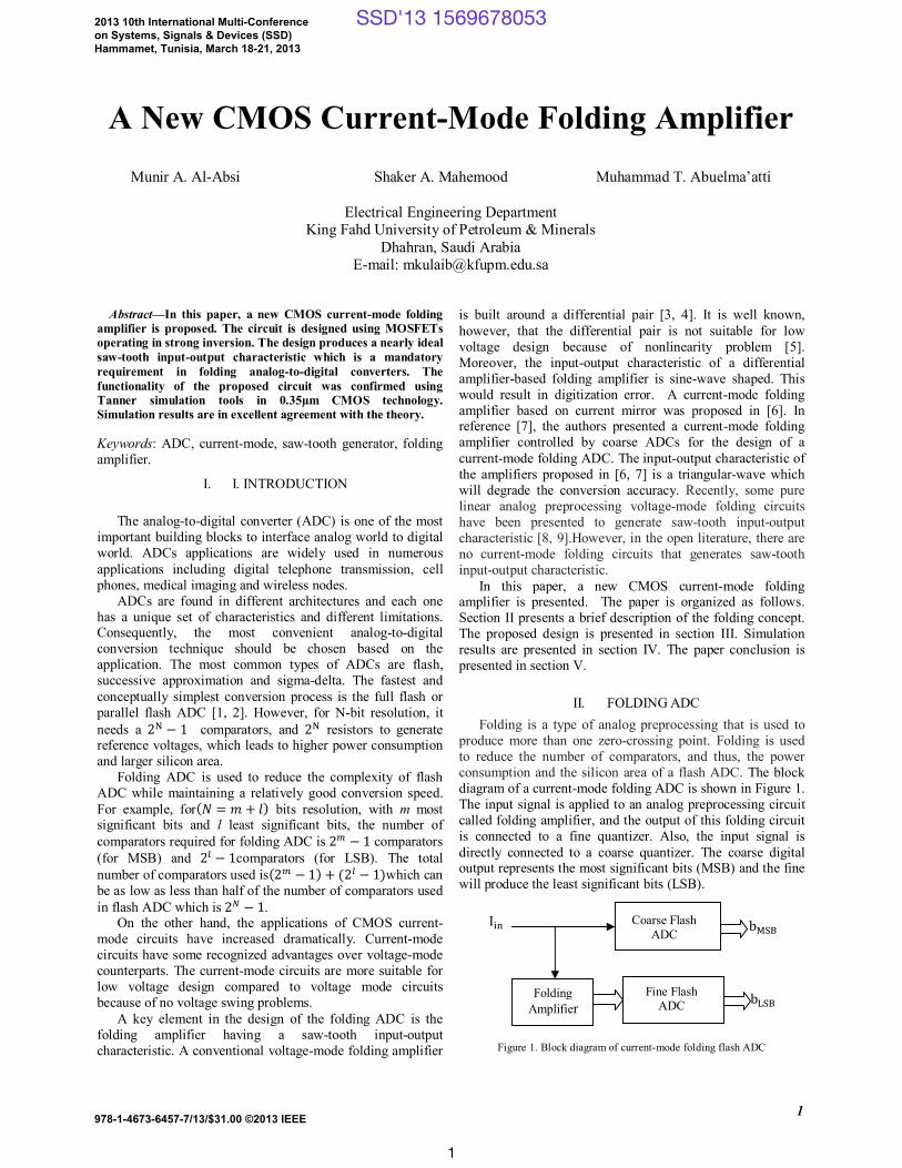
A New CMOS Current-Mode Folding Amplifier
Munir A. Al-Absi Shaker A. Mahemood Muhammad T. Abuelma’atti
Electrical Engineering Department
King Fahd University of Petroleum & Minerals Dhahran, Saudi Arabia
E-mail: [email protected]
Abstract—In this paper, a new CMOS current-mode folding
amplifier is proposed. The circuit is designed using MOSFETs operating in strong inversion. The design produces a nearly ideal saw-tooth input-output characteristic which is a mandatory requirement in folding analog-to-digital converters. The functionality of the proposed circuit was confirmed using Tanner simulation tools in 0.35µm CMOS technology. Simulation results are in excellent agreement with the theory.
Keywords: ADC, current-mode, saw-tooth generator, folding amplifier.
I. I. INTRODUCTION
The analog-to-digital converter (ADC) is one of the most important building blocks to interface analog world to digital world. ADCs applications are widely used in numerous applications including digital telephone transmission, cell phones, medical imaging and wireless nodes.
ADCs are found in different architectures and each one has a unique set of characteristics and different limitations. Consequently, the most convenient analog-to-digital conversion technique should be chosen based on the application. The most common types of ADCs are flash, successive approximation and sigma-delta. The fastest and conceptually simplest conversion process is the full flash or parallel flash ADC [1, 2]. However, for N-bit resolution, it needs a 2 − 1 comparators, and 2 resistors to generate reference voltages, which leads to higher power consumption and larger silicon area.
Folding ADC is used to reduce the complexity of flash ADC while maintaining a relatively good conversion speed. For example, for(푁 = 푚 + 푙) bits resolution, with m most significant bits and l least significant bits, the number of comparators required for folding ADC is 2 − 1 comparators (for MSB) and 2 − 1comparators (for LSB). The total number of comparators used is(2 − 1) + (2 − 1)which can be as low as less than half of the number of comparators used in flash ADC which is 2 − 1.
On the other hand, the applications of CMOS current-mode circuits have increased dramatically. Current-mode circuits have some recognized advantages over voltage-mode counterparts. The current-mode circuits are more suitable for low voltage design compared to voltage mode circuits because of no voltage swing problems.
A key element in the design of the folding ADC is the folding amplifier having a saw-tooth input-output characteristic. A conventional voltage-mode folding amplifier
is built around a differential pair [3, 4]. It is well known, however, that the differential pair is not suitable for low voltage design because of nonlinearity problem [5]. Moreover, the input-output characteristic of a differential amplifier-based folding amplifier is sine-wave shaped. This would result in digitization error. A current-mode folding amplifier based on current mirror was proposed in [6]. In reference [7], the authors presented a current-mode folding amplifier controlled by coarse ADCs for the design of a current-mode folding ADC. The input-output characteristic of the amplifiers proposed in [6, 7] is a triangular-wave which will degrade the conversion accuracy. Recently, some pure linear analog preprocessing voltage-mode folding circuits have been presented to generate saw-tooth input-output characteristic [8, 9].However, in the open literature, there are no current-mode folding circuits that generates saw-tooth input-output characteristic.
In this paper, a new CMOS current-mode folding amplifier is presented. The paper is organized as follows. Section II presents a brief description of the folding concept. The proposed design is presented in section III. Simulation results are presented in section IV. The paper conclusion is presented in section V.
II. FOLDING ADC Folding is a type of analog preprocessing that is used to
produce more than one zero-crossing point. Folding is used to reduce the number of comparators, and thus, the power consumption and the silicon area of a flash ADC. The block diagram of a current-mode folding ADC is shown in Figure 1. The input signal is applied to an analog preprocessing circuit called folding amplifier, and the output of this folding circuit is connected to a fine quantizer. Also, the input signal is directly connected to a coarse quantizer. The coarse digital output represents the most significant bits (MSB) and the fine will produce the least significant bits (LSB).
Figure 1. Block diagram of current-mode folding flash ADC
I b
b Folding Amplifier
Coarse Flash ADC
Fine Flash ADC
SSD'13 1569678053
1
2013 10th International Multi-Conference on Systems, Signals & Devices (SSD) Hammamet, Tunisia, March 18-21, 2013
978-1-4673-6457-7/13/$31.00 ©2013 IEEE
1 2 3 4 5 6 7 8 91011121314151617181920212223242526272829303132333435363738394041424344454647484950515253545556576061
2
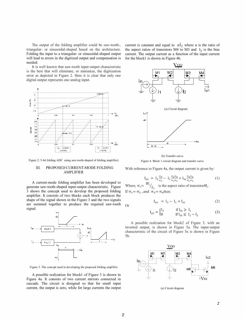
The output of the folding amplifier could be saw-tooth-, triangular- or sinusoidal-shaped based on the architecture. Folding the input to a triangular- or sinusoidal-shaped output will lead to errors in the digitized output and compensation is needed.
It is well known that saw-tooth input-output characteristic is the best that will eliminate, or minimize, the digitization error as depicted in Figure 2. Here it is clear that only one digital output represents one analog input.
Figure 2. 5-bit folding ADC using saw-tooth-shaped of folding amplifier)
III. PROPOSED CURRENT-MODE FOLDING AMPLIFIER
A current-mode folding amplifier has been developed to
generate saw-tooth-shaped input-output characteristic. Figure 3 shows the concept used to develop the proposed folding amplifier. It consists of two blocks each block produces the shape of the signal shown in the Figure 3 and the two signals are summed together to produce the required saw-tooth signal.
Figure 3. The concept used in developing the proposed folding amplifier
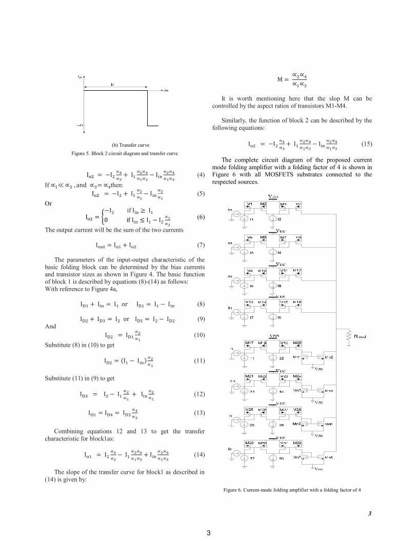
A possible realization for block1 of Figure 3 is shown in Figure 4a. It consists of two current mirrors connected in cascade. The circuit is designed so that for small input current, the output is zero, while for large currents the output
current is constant and equal to 훼I2 where α is the ratio of the aspect ratios of transistors M4 to M3 and I is the bias current. The output current as a function of the input current for the block1 is shown in Figure 4b.
(a) Circuit diagram
(b) Transfer curve
Figure 4. Block 1 circuit diagram and transfer curve
With reference to Figure 4a, the output current is given by:
I = I ∝∝−I ∝ ∝
∝ ∝+ I ∝ ∝
∝ ∝(1)
Where, ∝ =푊 퐿 is the aspect ratio of transistor푀 . If ∝ =∝ , and ∝ =∝ then:
I = I − I + I (2) Or
I = I ifI ≥ I 0ifI ≤ I − I (3)
A possible realization for block2 of Figure 3, with an
inverted output, is shown in Figure 5a. The input-output characteristic of the circuit of Figure 5a is shown in Figure 5b.
(a) Circuit diagram
2
1 2 3 4 5 6 7 8 91011121314151617181920212223242526272829303132333435363738394041424344454647484950515253545556576061
3
(b) Transfer curve
Figure 5. Block 2 circuit diagram and transfer curve
I = −I ∝
∝+I ∝ ∝
∝ ∝− I ∝ ∝
∝ ∝(4)
If ∝ ≪∝ , and ∝ =∝ then: I = −I +I ∝
∝− I ∝
∝(5)
Or
I =−I ifI ≥ I 0ifI ≤ I − I ∝
∝(6)
The output current will be the sum of the two currents
I = I + I (7)
The parameters of the input-output characteristic of the basic folding block can be determined by the bias currents and transistor sizes as shown in Figure 4. The basic function of block 1 is described by equations (8)-(14) as follows: With reference to Figure 4a,
I + I = I orI = I − I (8)
I + I = I orI = I − I (9)
And I = I ∝
∝(10)
Substitute (8) in (10) to get
I = (I − I )∝∝(11)
Substitute (11) in (9) to get
I = I − I ∝∝+ I ∝
∝ (12)
I = I = I ∝
∝(13)
Combining equations 12 and 13 to get the transfer
characteristic for block1as:
I = I ∝∝−I ∝ ∝
∝ ∝+ I ∝ ∝
∝ ∝(14)
The slope of the transfer curve for block1 as described in
(14) is given by:
M =∝ ∝∝ ∝
It is worth mentioning here that the slop M can be
controlled by the aspect ratios of transistors M1-M4.
Similarly, the function of block 2 can be described by the following equations:
I = −I ∝∝+I ∝ ∝
∝ ∝− I ∝ ∝
∝ ∝(15)
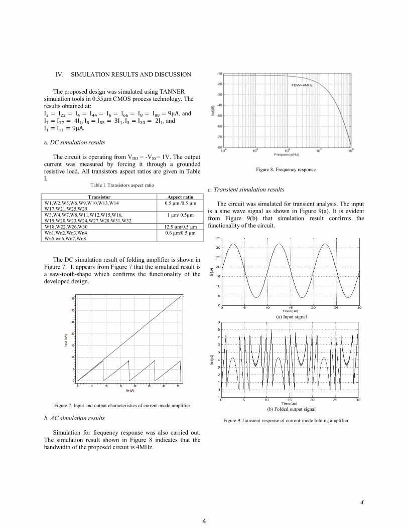
The complete circuit diagram of the proposed current
mode folding amplifier with a folding factor of 4 is shown in Figure 6 with all MOSFETS substrates connected to the respected sources.
Figure 6. Current-mode folding amplifier with a folding factor of 4
3
1 2 3 4 5 6 7 8 91011121314151617181920212223242526272829303132333435363738394041424344454647484950515253545556576061
4
IV. SIMULATION RESULTS AND DISCUSSION
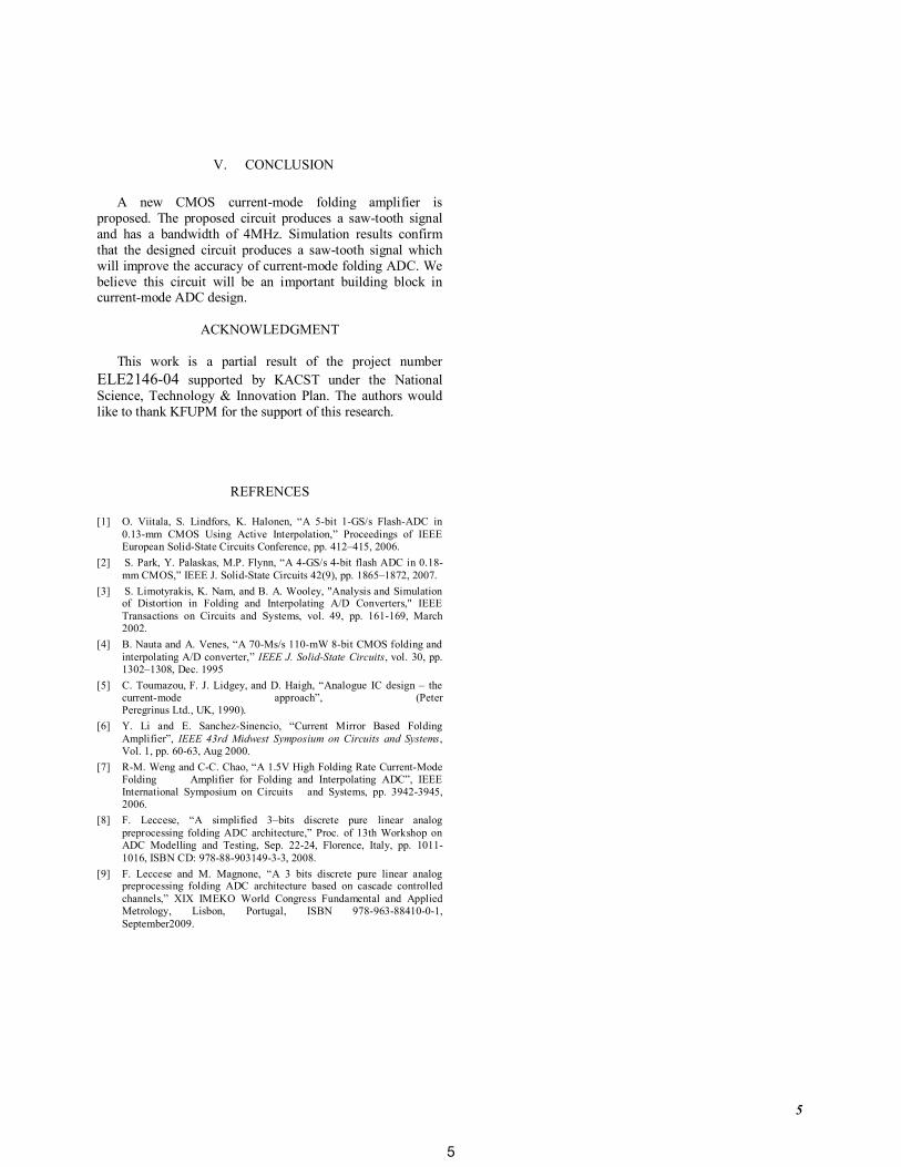
The proposed design was simulated using TANNER simulation tools in 0.35μm CMOS process technology. The results obtained at: I = I = I = I = I = I = I = I = 9μA, and I = I = 4I , I = I =3I , I = I = 2I , and I = I = 9μA. a. DC simulation results
The circuit is operating from VDD = -VSS= 1V. The output current was measured by forcing it through a grounded resistive load. All transistors aspect ratios are given in Table I.
Table I. Transistors aspect ratio
Transistor Aspect ratio W1,W2,W5,W6,W9,W10,W13,W14 W17,W21,W25,W29
0.5 µm /0.5 µm
W3,W4,W7,W8,W11,W12,W15,W16, W19,W20,W23,W24,W27,W28,W31,W32
1 µm/ 0.5µm
W18,W22,W26,W30 12.5 µm/0.5 µm Wn1,Wn2,Wn3,Wn4 Wn5,wn6,Wn7,Wn8
0.6 µm/0.5 µm
The DC simulation result of folding amplifier is shown in Figure 7. It appears from Figure 7 that the simulated result is a saw-tooth-shape which confirms the functionality of the developed design.
Figure 7. Input and output characteristics of current-mode amplifier
b. AC simulation results
Simulation for frequency response was also carried out. The simulation result shown in Figure 8 indicates that the bandwidth of the proposed circuit is 4MHz.
Figure 8. Frequency responce
c. Transient simulation results
The circuit was simulated for transient analysis. The input is a sine wave signal as shown in Figure 9(a). It is evident from Figure 9(b) that simulation result confirms the functionality of the circuit.
(a) Input signal
(b) Folded output signal
Figure 9.Transient response of current-mode folding amplifier
4
1 2 3 4 5 6 7 8 91011121314151617181920212223242526272829303132333435363738394041424344454647484950515253545556576061
5
V. CONCLUSION
A new CMOS current-mode folding amplifier is proposed. The proposed circuit produces a saw-tooth signal and has a bandwidth of 4MHz. Simulation results confirm that the designed circuit produces a saw-tooth signal which will improve the accuracy of current-mode folding ADC. We believe this circuit will be an important building block in current-mode ADC design.
ACKNOWLEDGMENT
This work is a partial result of the project number ELE2146-04 supported by KACST under the National Science, Technology & Innovation Plan. The authors would like to thank KFUPM for the support of this research.
REFRENCES [1] O. Viitala, S. Lindfors, K. Halonen, “A 5-bit 1-GS/s Flash-ADC in
0.13-mm CMOS Using Active Interpolation,” Proceedings of IEEE European Solid-State Circuits Conference, pp. 412–415, 2006.
[2] S. Park, Y. Palaskas, M.P. Flynn, “A 4-GS/s 4-bit flash ADC in 0.18-mm CMOS,” IEEE J. Solid-State Circuits 42(9), pp. 1865–1872, 2007.
[3] S. Limotyrakis, K. Nam, and B. A. Wooley, "Analysis and Simulation of Distortion in Folding and Interpolating A/D Converters," IEEE Transactions on Circuits and Systems, vol. 49, pp. 161-169, March 2002.
[4] B. Nauta and A. Venes, “A 70-Ms/s 110-mW 8-bit CMOS folding and interpolating A/D converter,” IEEE J. Solid-State Circuits, vol. 30, pp. 1302–1308, Dec. 1995
[5] C. Toumazou, F. J. Lidgey, and D. Haigh, “Analogue IC design – the current-mode approach”, (Peter Peregrinus Ltd., UK, 1990).
[6] Y. Li and E. Sanchez-Sinencio, “Current Mirror Based Folding Amplifier”, IEEE 43rd Midwest Symposium on Circuits and Systems, Vol. 1, pp. 60-63, Aug 2000.
[7] R-M. Weng and C-C. Chao, “A 1.5V High Folding Rate Current-Mode Folding Amplifier for Folding and Interpolating ADC”, IEEE International Symposium on Circuits and Systems, pp. 3942-3945, 2006.
[8] F. Leccese, “A simplified 3–bits discrete pure linear analog preprocessing folding ADC architecture,” Proc. of 13th Workshop on ADC Modelling and Testing, Sep. 22-24, Florence, Italy, pp. 1011-1016, ISBN CD: 978-88-903149-3-3, 2008.
[9] F. Leccese and M. Magnone, “A 3 bits discrete pure linear analog preprocessing folding ADC architecture based on cascade controlled channels,” XIX IMEKO World Congress Fundamental and Applied Metrology, Lisbon, Portugal, ISBN 978-963-88410-0-1, September2009.
5