Embed Size (px)
Citation preview
Abstract—A small-signal amplifier with three identical
MOSFETs in Darlington’s topology is proposed and
qualitatively analyzed perhaps for the first time. Unlike CS-
MOSFET amplifiers, the voltage gain of the proposed circuit is
found considerably higher than unity. This amplifier can be
used to amplify audio range signal excursions swinging in 0.1-
2mV range. In the narrow-band performance range, the
proposed amplifier produces simultaneously high voltage and
current gains with low harmonic distortion. These properties
offer a flexible application range to the proposed circuit as
high-voltage-narrow-band amplifier in permissible audio-
frequency range. An additional biasing resistance RA is to be
essentially used in the proposed circuit to maintain its
voltage/current amplification property. Variations in voltage
gain as a function of frequency and different biasing
resistances, temperature dependency of performance
parameters like voltage gain, bandwidth, current gain,
input/output noises and total harmonic distortion of the
amplifier are perused to provide a wide spectrum to the
qualitative studies.
Index Terms—Small signal RC coupled amplifiers,
darlington amplifiers, common Source MOS amplifiers, triple
darlington amplifiers, MOSFET darlington pairs.
I. INTRODUCTION
In general, MOS transistors act as good amplifiers for
radio frequency integrated circuits when operated in the
saturation region (under specific characteristics) and exhibit
capacity to provide high voltage, current and power gains
[1], [2]. Concurrently „Common Source MOSFET‟ has been
explored to amplify small-signals with its specific
characteristic of high input impedance, low output
impedance, high current gain and a voltage gain greater than
unity [3]-[6]. Numerous researches explored this MOSFET
configuration suitable for developing high speed switching
circuits, memory segments, logic gates, buffer amplifiers,
power amplifiers and trans-conductance amplifiers [1]-[9].
However, use of CS-MOSFET in Darlington‟s topology to
develop small-signal audio range amplifiers is still to be
established [5], [10]. In this sequence, authors developed
two small-signal amplifier circuits using MOSFETs in
Darlington pair and explored them as high voltage gain and
wideband amplifiers respectively [5].
In the present manuscript, authors proposed a novel
circuit of high voltage / high current gain audio-range small-
Manuscript received April 27, 2013; revised July 1, 2013.
Sachchida Nand Shukla, Senior member IACSIT, is with the
Department of Physics and Electronics of Dr. Ram Manohar Lohia Avadh
University, Faizabad-224001, U.P., India (e-mail:
Susmrita Srivastava is with the Department of Physics and Electronics
of Dr. Ram Manohar Lohia Avadh University, Faizabad - 224001, U.P.,
India(e-mail: susmrita @rediffmail.com)
signal amplifier by placing identical CS-MOSFETs in
Triple Darlington configuration [11].
Dependency of qualitative performance of the proposed
amplifier on various biasing parameters, biasing supply and
operational frequency is analyzed and compared with that of
high voltage gain Darlington pair MOSFET amplifier [5].
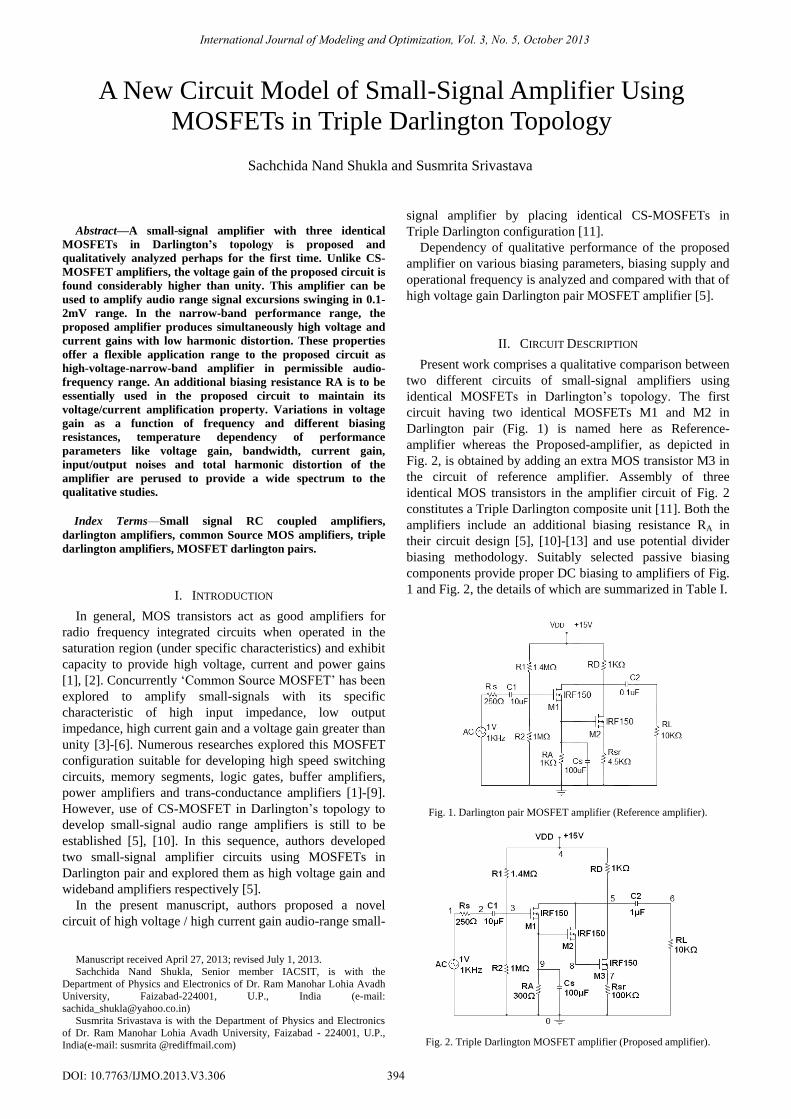
II. CIRCUIT DESCRIPTION
Present work comprises a qualitative comparison between
two different circuits of small-signal amplifiers using
identical MOSFETs in Darlington‟s topology. The first
circuit having two identical MOSFETs M1 and M2 in
Darlington pair (Fig. 1) is named here as Reference-
amplifier whereas the Proposed-amplifier, as depicted in
Fig. 2, is obtained by adding an extra MOS transistor M3 in
the circuit of reference amplifier. Assembly of three
identical MOS transistors in the amplifier circuit of Fig. 2
constitutes a Triple Darlington composite unit [11]. Both the
amplifiers include an additional biasing resistance RA in
their circuit design [5], [10]-[13] and use potential divider
biasing methodology. Suitably selected passive biasing
components provide proper DC biasing to amplifiers of Fig.
1 and Fig. 2, the details of which are summarized in Table I.
Fig. 1. Darlington pair MOSFET amplifier (Reference amplifier).
Fig. 2. Triple Darlington MOSFET amplifier (Proposed amplifier).
A New Circuit Model of Small-Signal Amplifier Using
MOSFETs in Triple Darlington Topology
Sachchida Nand Shukla and Susmrita Srivastava
International Journal of Modeling and Optimization, Vol. 3, No. 5, October 2013
394DOI: 10.7763/IJMO.2013.V3.306
PSpice simulation (Student version 9.2) is performed to
carry out present investigations [5], [10]-[14]. Observations
are procured by feeding the amplifier circuits with 1V AC
input signal source, from which, a small-distortion-less AC
signal of 1mV for both the amplifiers at 1KHz frequency is
drawn as input for amplification purpose. The amplifier of
Fig. 1 is found to provide undistorted output for 0.1-10mV
AC input signal at 1KHz frequency and is biased with +15V
DC supply whereas proposed amplifier of Fig. 2 produces
distortion-less results for 0.1-2mV AC input at similar
frequency and DC biasing supply.
TABLE I: COMPONENT DETAILS OF THE CIRCUITS UNDER DISCUSSION
COMPONENTS DESCRIPTION Fig.1 Fig.2
M1, M2: Power MOSFET (VTO=2.831) IRF150 IRF150
M3: Power MOSFET (VTO=2.831) - IRF150
RS: Source Resistance 250Ω 250Ω
R1: Biasing Resistance 1.4MΩ 1.4MΩ
R2: Biasing Resistance 1MΩ 1MΩ
RD: Drain Biasing Resistance 1KΩ 1KΩ
RSR: Source Biasing Resistance 4.5KΩ 100KΩ
RA: Additional Biasing Resistance 1 KΩ 300Ω
RL: Load Resistance 10KΩ 10KΩ
C1: Coupling Capacitor 10 µF 10 µF
C2: Coupling Capacitor 0.1 µF 1 µF
CS: Source By-pass Capacitor 100µF 100 µF
DC Biasing Supply +15V DC +15V DC
AC input signal range for purposeful
amplification at 1KHz frequency
0.1-10mV 0.1-2mV
III. RESULTS AND DISCUSSIONS
The amplifiers of Fig. 1 and Fig. 2 are found to provide
fair and distortion-less results for 0.1-10mV and 0.1-2mV
AC input signals respectively in 100 Hz to 100 KHz input
frequency range at +15V DC biasing voltage. However,
when DC biasing to the proposed amplifier is changed to
+12V, the circuit provides distortion-less results for 0.1-
15mV AC input signal in the similar range of frequency.
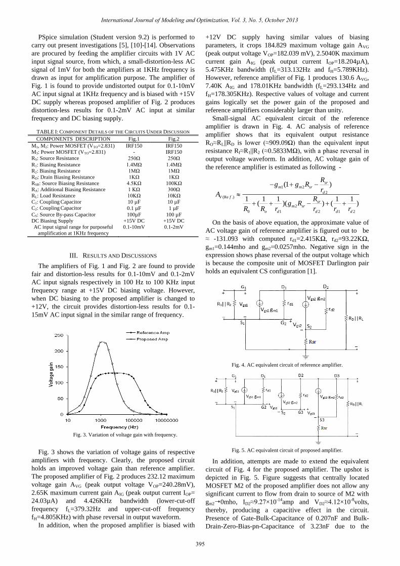
Fig. 3. Variation of voltage gain with frequency.
Fig. 3 shows the variation of voltage gains of respective
amplifiers with frequency. Clearly, the proposed circuit
holds an improved voltage gain than reference amplifier.
The proposed amplifier of Fig. 2 produces 232.12 maximum
voltage gain AVG (peak output voltage VOP=240.28mV),
2.65K maximum current gain AIG (peak output current IOP=
24.03µA) and 4.426KHz bandwidth (lower-cut-off
frequency fL=379.32Hz and upper-cut-off frequency
fH=4.805KHz) with phase reversal in output waveform.
In addition, when the proposed amplifier is biased with
+12V DC supply having similar values of biasing
parameters, it crops 184.829 maximum voltage gain AVG
(peak output voltage VOP=182.039 mV), 2.5040K maximum
current gain AIG (peak output current IOP=18.204µA),
5.475KHz bandwidth (fL=313.132Hz and fH=5.789KHz).
However, reference amplifier of Fig. 1 produces 130.6 AVG,
7.40K AIG and 178.01KHz bandwidth (fL=293.134Hz and
fH=178.305KHz). Respective values of voltage and current
gains logically set the power gain of the proposed and
reference amplifiers considerably larger than unity.
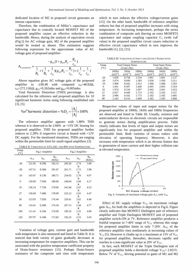
Small-signal AC equivalent circuit of the reference
amplifier is drawn in Fig. 4. AC analysis of reference
amplifier shows that its equivalent output resistance
RO≈RL||RD is lower (≈909.09Ω) than the equivalent input
resistance RI≈R1||R2 (≈0.5833MΩ), with a phase reversal in
output voltage waveform. In addition, AC voltage gain of
the reference amplifier is estimated as following -
1 2
2(Re .)
2
0 1 2 1 2
(1 )
1 1 1 1 1( )( ) ( )
srm m sr
dV f
srm sr
o d d d d
Rg g R
rA
Rg R
R R r r r r
On the basis of above equation, the approximate value of
AC voltage gain of reference amplifier is figured out to be
≈ -131.093 with computed rd1=2.415KΩ, rd2=93.22KΩ,
gm1=0.144mho and gm2=0.0257mho. Negative sign in the
expression shows phase reversal of the output voltage which
is because the composite unit of MOSFET Darlington pair
holds an equivalent CS configuration [1].
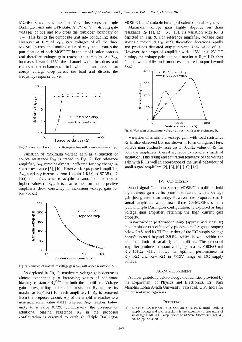
Fig. 4. AC equivalent circuit of reference amplifier.
Fig. 5. AC equivalent circuit of proposed amplifier.
In addition, attempts are made to extend the equivalent
circuit of Fig. 4 for the proposed amplifier. The upshot is
depicted in Fig. 5. Figure suggests that centrally located
MOSFET M2 of the proposed amplifier does not allow any
significant current to flow from drain to source of M2 with
gm20mho, ID2≈9.27×10⁻¹⁴amp and VD2≈4.12×10⁻⁸volts,
thereby, producing a capacitive effect in the circuit.
Presence of Gate-Bulk-Capacitance of 0.207nF and Bulk-
Drain-Zero-Bias-pn-Capacitance of 3.23nF due to the
International Journal of Modeling and Optimization, Vol. 3, No. 5, October 2013
395
dedicated location of M2 in proposed circuit generates an
intense capacitance.
Therefore, the combination of Miller‟s capacitance and
capacitance due to centrally located MOSFET M2 of the
proposed amplifier causes an effective reduction in the
bandwidth. Hence, during the analysis of equivalent circuit
(Fig.5) for AC voltage gain, M2 of the proposed amplifier
would be treated as absent. This estimation suggests
following expression for the approximate value of AC
voltage gain of proposed amplifier-
1 3
3( )
3
0 0 1 3 1 3
(1 )
1 1 1 1 1( )( ) ( )
srm m sr
dV proposed
srm sr
d d d d
Rg g R
rA
Rg R
R R r r r r
Above equation gives AC voltage gain of the proposed
amplifier to -238.48 with computed rd1=48.82Ω,
rd3=272.11KΩ, gm1=0.262mho and gm3=0.005mho.
Total Harmonic Distortion (THD) percentage is also
calculated for the reference and proposed amplifiers for 10
significant harmonic terms using following established rule
[3], [5].
1
% % 100%nth
n
An harmonic distortion D
A
The reference amplifier appears with 1.88% THD
whereas it is observed to be 2.84% at +15V DC biasing for
proposed amplifier. THD for proposed amplifier further
reduces to 2.28% if respective circuit is biased with +12V
DC supply. For the mentioned situations, THDs are ranging
within the permissible limit for small-signal amplifiers [3].
TABLE II: VARIATION OF AVG,AIG AND BW WITH TEMPERATURE
Temp.
(°C) Fig.1 Amplifier Fig.2 Amplifier
AVG AIG
BW
(KHz) AVG AIG
BW
(KHz)
-30 151.85 8.59K 182.53 269.26 2.74
K
3.89
-20 147.51 8.36K 181.67 261.71 2.72
K
3.98
-10 143.47 8.13K 180.71 254.65 2.70
K
4.07
0 139.69 7.92K 180.06 248.04 2.69
K
4.17
10 136.14 7.72K 178.06 241.84 2.67
K
4.23
27 130.60 7.40K 178.00 232.12 2.65
K
4.47
50 123.93 7.02K 176.44 220.41 2.62
K
4.46
80 116.41 6.58K 176.34 207.15 2.58
K
4.77
100 111.41 6.33K 176.09 199.35 2.55
K
4.86
120 107.97 6.10K 173.82 192.25 2.53
K
5.03
Variation of voltage gain, current gain and bandwidth
with temperature is also measured and listed in Table II. It is
noticed that both variety of gains gradually decreases at
increasing temperature for respective amplifiers. This can be
associated with the positive temperature coefficient property
of Drain-Source resistance [15]. Perhaps Drain-Source
resistance of the composite unit rises with temperature
which in turn reduces the effective voltage/current gains
[15]. On the other hand, bandwidth of reference amplifier
reduces but that of proposed amplifier increases with rising
temperature. At increasing temperature, perhaps the series
combination of composite unit (having an extra MOSFET)
capacitance and output coupling capacitor C2 (with 1uF
value) in the proposed amplifier circuit causes reduction in
effective circuit capacitance which in turn improves the
bandwidth [1], [2], [15].
TABLE III: VARIATION OF INPUT AND OUTPUT NOISES WITH
TEMPERATURE
Temp.
(OC)
Total Output Noise
(Volts/√Hz)
Total Input Noise
(Volts/√Hz)
100Hz
(x10-9)
1KHz
(x10-10)
1MHz
(x10-14)
100Hz
(x10-9)
1KHz
(x10-9)
1MHz
(x10-9)
-30 1.839 8.758 1.554 1.891 1.891 3.137
-20 1.874 8.699 1.583 1.930 1.930 3.211
-10 1.908 8.642 1.612 1.968 1.968 3.283
0 1.941 8.587 1.640 2.005 2.005 3.354
10 1.974 8.534 1.667 2.042 2.041 3.423
27 2.027 8.449 1.713 2.102 2.102 3.537
50 2.096 8.342 1.773 2.182 2.182 3.685
80 2.182 8.216 1.849 2.282 2.282 3.868
Respective values of input and output noises for the
proposed amplifier at 100Hz, 1KHz and 1MHz frequencies
are observed and listed in Table III. Usually, resistors and
semiconductor devices in electronic circuits are responsible
to generate noises during amplification process. Table
clearly indicates that levels of input and output noises are
significantly low for proposed amplifier and within the
permissible limit. Both varieties of noises reduce with
elevation of operating frequency. Moreover, it also
increases with temperature which is an obvious feature due
to generation of more carriers and their higher collision rate
at elevated temperature.
Fig. 6. Variation of maximum voltage gain AVG with VDD。
Effect of DC supply voltage VCC on maximum voltage
gain AVG for both the amplifiers is depicted in Fig.6. Figure
clearly indicates that MOSFET Darlington pair of reference
amplifier and Triple Darlington MOSFET unit of proposed
amplifier switch-ON at 7V. Reference amplifier produces a
fruitful response in 7-40V range of VCC whereas this range
for proposed amplifier limits to only 7-20V. AVG of the
reference amplifier rises nonlinearly at increasing values of
VCC [5]. However it climbs up to a maximum at 15V of VCC
for proposed amplifier, thereafter, decreases rapidly and
reaches to a non-significant value at 20V of VCC.
In fact, each MOSFET of the Triple Darlington unit of
proposed amplifier holds a threshold voltage VTO= 2.831V.
Below 7V of VCC, driving potential to gates of M1 and M2
International Journal of Modeling and Optimization, Vol. 3, No. 5, October 2013
396
MOSFETs are found less than VTO. This keeps the triple
Darlington unit into OFF state. At 7V of VCC, driving gate
voltages of M1 and M3 cross the forbidden boundary of
VTO. This brings the composite unit into conducting state.
However at 15V of VCC, gate voltages of all the three
MOSFETs cross the limiting value of VTO. This ensures the
participation of each MOSFET in the amplification process
and therefore voltage gain reaches to a maxim. As VCC
increases beyond 15V, the channel width broadens and
causes sudden enhancement in ID which in turn forces for an
abrupt voltage drop across the load and distorts the
frequency response curve.
Fig. 7. Variation of maximum voltage gain AVG with source resistance RSR。
Variation of maximum voltage gain as a function of
source resistance RSR is traced in Fig. 7. For reference
amplifier, AVG remains almost unaffected for any change in
source resistance [5], [10]. However for proposed amplifier,
AVG suddenly increases from 1.44 (at 1 KΩ) to187.38 (at 2
KΩ), thereafter, tends to acquire a saturation tendency at
higher values of RSR. It is also to mention that respective
amplifiers show constancy in maximum voltage gain for
RSR>10KΩ.
Fig. 8. Variation of maximum voltage gain AVG with added resistance RA。
As depicted in Fig. 8, maximum voltage gain decreases
almost exponentially at increasing values of additional
biasing resistance RA(5,10) for both the amplifiers. Voltage
gain corresponding to the added resistance RA acquires its
maxim at RA≤1KΩ for each amplifier. If RA is removed
from the proposed circuit, AIG of the amplifier reaches to a
non-significant value 0.013 whereas AVG reaches below
unity to a value 0.729. Conclusively, the presence of
additional biasing resistance RA in the proposed
configuration is essential to establish „Triple Darlington
MOSFET unit‟ suitable for amplification of small-signals.
Maximum voltage gain highly depends on drain
resistance RD [1], [2], [5], [10]. Its variation with RD is
depicted in Fig. 9. For reference amplifier, voltage gain
attains a maxim at RD=3KΩ, thereafter, decreases rapidly
and produces distorted output beyond 4KΩ value of RD.
However, for proposed amplifier with +15V or +12V DC
biasing, the voltage gain attains a maxim at RD=1KΩ, then
falls down rapidly and produces distorted output beyond
2KΩ.
Fig. 9. Variation of maximum voltage gain AVG with drain resistance RD。
Variation of maximum voltage gain with load resistance
RL is also observed but not shown in form of figure. Here,
voltage gain gradually rises up to 100KΩ value of RL for
both the amplifiers, thereafter, tends to acquire a mark of
saturation. This rising and saturation tendency of the voltage
gain with RL is well in accordance of the usual behaviour of
small signal amplifiers [2], [5], [6], [10]-[13].
IV. CONCLUSION
Small-signal Common Source MOSEFT amplifiers hold
high current gain as its prominent feature with a voltage
gain just greater than unity. However, the proposed small-
signal amplifier, which uses three CS-MOSFETs in a
typical Triple Darlington configuration, is explored as high
voltage gain amplifier, retaining the high current gain
property.
In narrowband performance range (approximately 5KHz)
this amplifier can effectively process small-signals ranging
below 2mV and its THD at either of the DC supply voltage
doesn‟t exceed beyond 2.84%, which is well within the
tolerance limit of small-signal amplifiers. The proposed
amplifier produces constant voltage gain at RL>100KΩ and
RSR>10KΩ while shows its optimal performance at
RA<1KΩ and RD=1KΩ in 7-15V range of DC supply
voltage.
ACKNOWLEDGEMENT
Authors gratefully acknowledge the facilities provided by
the Department of Physics and Electronics, Dr. Ram
Manohar Lohia Avadh University, Faizabad, U.P., India for
the present investigations.
REFERENCES
[1] E. Vernon, D. B Ryson, E. S. Orr, and S. N. Mohammad, “Role of
supply voltage and load capacitors in the experimental operations of
small signal MOSFET amplifiers,” Solid State Electronics, vol. 45,
no. 12, pp. 2033, 2001.
International Journal of Modeling and Optimization, Vol. 3, No. 5, October 2013
397
[2] E. Vernon, D. Bryson, E. S. Orr, and S. N. Mohammad,
“Experimental studies of frequency response of small signal
MOSFET amplifiers,” Solid State Electronics, vol. 46, no. 2, pp. 287-
294, 2002.
[3] R. L. Boylestad and L. Nashelsky, “Electronic Devices and Circuit
Theory,” Pearson Education Asia, 3rd ed., 2002, pp. 263, 307, 600.
[4] P. McGregor, J. Mena, and C. A. T. Salama, “Small signal high
frequency performance of power MOS transistors,” Solid State
Electronics, vol. 27, no. 5, pp. 419, 1984.
[5] S. Srivastava, B. Pandey, S. N. Tiwari, J. Singh, and S. N. Shukla,
“Qualitative analysis of MOS based Darlington Pair Amplifiers,”
Bulletin of Pure and Applied Science, vol. 30D (Physics), no. 2, pp.
195, 2011.
[6] E. Vernon, D. Bryson, A. Motayed, and S. N. Mohammad,
“Experimental investigation of factors influencing design of small
signal CMOS amplifiers,” Solid State Electronics, vol. 45, no. 1, pp.
63, 2001.
[7] P. M. Figueiredo and J. C. Vital, “The MOS capacitor amplifier,”
IEEE Transactions on Circuits and Systems-II: Express Briefs, vol.
51, no. 3, March, 2004.
[8] B. Federico, E. A. M. Klumperink, and B. Nauta, “Generating All
Two-MOS-Transistor Amplifiers Leads to New Wide-Band LNAs,”
IEEE Journal of Solid State Circuits, vol. 36, no. 7, pp. 1032, 2001.
[9] M. K. Kazimierczuk, “Class D Voltage-Switching MOSFET Power
Amplifier, Electronic Power Amplifications,” IEEE Proceeding B,
vol. 138, issue. 6, pp. 285, 1991.
[10] S. Srivastava, B. Pandey, S. N. Tiwari, J. Singh, and S. N. Shukla,
“Development of small-signal high voltage gain amplifier using
compound unit of BJT and MOSFET,” Acta Ciencia Indica, vol.
xxxviip, no. 4, pp. 431, 2011.
[11] S. N. Tiwari and S. N. Shukla, “Qualitative Analysis of Small Signal
Modified Darlington Pair and Triple Darlington Amplifiers,” Bulletin
of Pure and Applied Science, vol. 28D, no. 1, pp. 1, 2009.
[12] A. M. H. Sayed ElAhl, M. M. E. Fahmi, and S. N. Mohammad,
“Qualitative analysis of high frequency performance of modified
Darlington pair,” Solid State Electronics, vol. 46, pp. 593, 2002.
[13] S. N. Tiwari, B. Pandey, A. K. Dwivedi, and S. N. Shukla,
“Development of Small-Signal Amplifiers by Placing BJT and JFET
in Darlington Pair Configuration,” Journal of Ultra Scientist of
Physical Sciences, vol. 21, no. 3, pp. 509, 2009.
[14] M. H. Rashid, “Introduction to PSpice Using OrCAD for Circuits and
Electronics,” Pearson Education, 3rd ed., pp. 255-300, 2004.
[15] P. E. J. Dodge, “Power MOSFET Tutorial,” Application Note APT-
0403 Rev B, March 2, 2006
Sachchida Nand Shukla received his M.Sc. and Ph.D.
Degrees in Physics (Electronics) from Dr. Ram
Manohar Lohia Avadh University, Faizabad in 1988 and
1991 respectively. Presently he is working as Associate
Professor in the Department of Physics and Electronics
of Dr. Ram Manohar Lohia Avadh University, Faizabad,
U.P., India and actively engaged in researches related to
the Circuit designing and simulation. During last five
years, he published over 35 research papers in International/National
journals and Conference Proceedings on various topics of his current
research interest.
Susmrita Srivastava received her M.Sc. degree in
Electronics from Department of Physics and
Electronics of Dr. Ram Manohar Lohia Avadh
University, Faizabad, U.P., India in 2008. Presently she
is pursuing Ph.D. degree in Electronics and published
16 research papers on various topics of Circuit
designing and simulation in International /National
journals and Conference Proceedings.
International Journal of Modeling and Optimization, Vol. 3, No. 5, October 2013
398


![Modeling and Analysis of Induction Machines under Broken ... · 21 22 2 2 31 32 3 3 sr sr sr n sr e T sr rs sr sr sr n sr e ... Therefore the resistance matrix [R r]is a symmetric(n+1)](https://img.pdfslide.us/doc/110x75/5e83e33adae9df101c14911a/modeling-and-analysis-of-induction-machines-under-broken-21-22-2-2-31-32-3-3.jpg)