Embed Size (px)
Citation preview

Volume No: 1(2014), Issue No: 11 (November) November 2014 www.ijmetmr.com Page 451
ISSN No: 2348-4845International Journal & Magazine of Engineering,
Technology, Management and ResearchA Monthly Peer Reviewed Open Access International e-Journal
Abstract:
The dynamic voltage restorer (DVR) is one of the mod-ern devices used in distribution systems to protect consumers against sudden changes in voltage ampli-tude. In this paper, emergency control in distribution systems is discussed by using the proposed multifunc-tional DVR control strategy.
Also, the multi-loop controller using the Posicast and P+Resonant controllers is proposed in order to improve the transient response and eliminate the steady-state error in DVR response, respectively. The proposed al-gorithm is applied to some disturbances in load voltage caused by induction motors starting, and a three-phase short circuit fault.
Also, the capability of the proposed DVR has been test-ed to limit the downstream fault current. The current limitation will restore the point of common coupling (PCC) (the bus to which all feeders under study are connected) voltage and protect the DVR itself.
The innovation here is that the DVR acts as virtual im-pedance with the main aim of protecting the PCC volt-age during downstream fault without any problem in real power injection into the DVR. Simulation results show the capability of the DVR to control the emer-gency conditions of the distribution systems.
Index Terms:
Dynamic voltage restorer (DVR), Emergency control, voltage sag, voltage swells.
M ShobhaP.G Student Scholar,
Department of Electrical & Electronics Engineering,
Avanti Institute of Engineering & Technology, Makavaripalem,
Vishakhapatnam.
K.Durga RaoAssistant Professor,
Department of Electrical & Electronics Engineering,
Avanti Institute of Engineering & Technology, Makavaripalem,
Vishakhapatnam.
Tegala.Srinivasa RaoAssociate Professor,
Department of Electrical & Electronics Engineering,
Avanti Institute of Engineering & Technology, Makavaripalem,
Vishakhapatnam.
I.INTRODUCTION:
Voltage sag and voltage swell are two of the most impor¬tant power-quality (PQ) problems that encom-pass almost 80% of the distribution system PQ prob-lems [1] According to the IEEE 1959-1995 standard, voltage sag is the decrease of 0.1 to 0.9p.u. in the RMS voltage level at system frequency and with the dura-tion of half a cycle to 1 min [2]. Short circuits, starting large motors, sudden changes of load, and energiza-tion of trans¬formers arc the main causes of voltage sags [3].According to the definition and nature of volt-age sag, it can be found that this is a transient phenom-enon whose cause’s arc classified as low- or medium-frequency transient events [2].
In recent years, considering the use of sensitive devic-es in modern industries, different methods of compen-sation of voltage sags have been used. One of these methods is using the DVR to im¬prove the PQ and com-pensate the load voltage [6]-[13].Previous works have been done on different aspects of DVR performance, and different control strategies have been found. These methods mostly depend on the purpose of using DVR. In some methods, the main purpose is to detect and compensate for the voltage sag with minimum DVR ac-tive power injection |4J, [5].
Also, the in-phase compensation method can be used for sag and swell mitigation [6]. The multiline DVR can be used for eliminating the battery in the DVR struc-ture and control¬ling more than one line [7], [14J.
A New Approach to Multifunctional Dynamic Voltage Restorer Implementation for Emergency Control in
Distribution Systems

Volume No: 1(2014), Issue No: 11 (November) November 2014 www.ijmetmr.com Page 452
ISSN No: 2348-4845International Journal & Magazine of Engineering,
Technology, Management and ResearchA Monthly Peer Reviewed Open Access International e-Journal
Moreover, research has been made on using the DVR in medium level voltage [8J. Harmonic mitigation [9J and control of DVR under frequency variations [10J are also in the area of research. The closed-loop control with load voltage and current feedback is introduced as a simple method to control the DVR in [I5|. Also, Posicast and P+Res¬onant controllers can be used to improve the transient response and eliminate the steady-state error in DVR.
The Posicast con¬troller is a kind of step function with two parts and is used to improve the damping of the transient oscillations initiated at the start instant from the voltage sag. The P+Rcsonant con¬troller consists of a proportional function plus a resonant func¬tion and it eliminates the steady-state voltage tracking er-ror [16], The state feed forward and feedback methods [17], symmetrical components estimation 118J, robust control [19], and wavelet transform [20] have also been proposed as different methods of controlling the DVR.
In all of the aforementioned methods, the source of distur¬bance is assumed to be on the feeder which is parallel to the DVR feeder. In this paper, a multifunc-tional control system is proposed in which the DVR pro-tects the load voltage using Posi¬cast and P+Resonant controllers when the source of disturbance is the par-allel feeders. On the other hand, during a downstream fault, the equipment protects the PCC voltage, limits the fault current, and protects itself from large fault current.
Although this latest condition has been described in [11] using the flux control method, the DVR proposed there acts like a virtual in¬ductance with a constant val-ue so that it does not receive any active power during limiting the fault current. But in the pro¬posed method when the fault current passes through the DVR, it acts like series variable impedance unlike [11] where the equivalent impedance was a constant.
The basis of the proposed control strategy in this paper is that when the fault current does not pass through the DVR, an outer feedback loop of the load voltage with an inner feedback loop of the filter capacitor cur-rent will be used. Also, a feed forward loop will be used to improve the dynamic response of the load voltage. Moreover, to improve the transient response, the Posi¬cast controller and to eliminate the steady-state error, the P+Res¬onant controller are used.
But in case the fault current passes through the DVR, using the flux control algorithm [11], the se¬ries volt-age is injected in the opposite direction and, therefore, the DVR acts like series variable impedance.
Fig.1. Typical DVR-connected distribution system.
The remainder of this paper is organized as follows: The gen¬eral operation of DVR and its state space de-scription arc provided in Section 11. The closed-loop control using Posicast and P+Resonant controllers has been presented in Section III. In Section IV, the mul-tifunctional DVR is introduced. The basis of the pro-posed control method is described in Section V. Finally, the simulation results are provided in Section VI which shows that the control capability of the proposed DVR system is satisfactory.
A. DVR Components:
A typical DVR-connected distribution system is shown in Fig.1, where the DVR consists of essentially a series-connected injection transformer, a voltage-source in-verter, an inverter output filter, and an energy storage device that is connected to the dc link. Before injecting the inverter output to the system, it must be filtered so that harmonics due to switching function in the invert-er are eliminated. It should be noted that when using the DVR in real situations, the injection transformer will be connected in parallel with a bypass switch (Fig. 1).
When there is no disturbances in voltage, the injection transformer (hence, the DVR) will be short circuited by this switch to minimize losses and maximize cost effec-tiveness. Also, this switch can be in the form of two parallel thyristors, as they have high on and off speed [21].

Volume No: 1(2014), Issue No: 11 (November) November 2014 www.ijmetmr.com Page 453
ISSN No: 2348-4845International Journal & Magazine of Engineering,
Technology, Management and ResearchA Monthly Peer Reviewed Open Access International e-Journal
A financial assessment of voltage sag events and use of flexible ac transmission systems (FACTS) devices, such as DVR, to mitigate them is provided in [22]. It is obvious that the flexibility of the DVR output depends on the switching accuracy of the pulse width modula-tion (PWM) scheme and the control method. The PWM generates sinusoidal signals by comparing a sinusoidal wave with a saw tooth wave and sending appropriate signals to the inverter switches. A further detailed de-scription about this scheme can be found in.
B. Basic Operational Principle of DVR:
The DVR system shown in Fig.1, controls the load volt-age by injecting an appropriate voltage phasor in series with the system using the injection series transformer. In most of the sag compensation techniques, it is nec-essary that during compensation, the DVR injects some active power to the system. Therefore, the capacity of the storage unit can be a limiting factor in compensa-tion, especially during long-term voltage sags.
Fig. 2. Phasor diagram of the electrical conditions dur-ing voltage sag.
‘The phasor diagram in Fig.2, shows the electrical con-ditions during voltage sag, where, for clarity, only one phase is shown. Voltages V1, V2, and VDVR are the source-side voltage, the load- side voltage, and the DVR injected voltage, respectively. Also, the operators I,∅,δ and a are the load current, the load power factor angle, the source phase voltage angle, and the voltage phase advance angle, respectively [24]. It should be noted that in addition to the in-phase injection technique, an-other technique, namely “the phase advance voltage compensation technique” is also used [24]. One of the advantages of this method over the in-phase method is that less active power should be transferred from the storage unit to the distribution system.
This results in compensation for deeper sags or sags with longer durations.
Due to the existence of semiconductor switches in the DVR inverter, this piece of equipment is nonlinear. How-ever, the state equations can be linear zed using linear-ization techniques. The dynamic characteristic of the DVR is influenced by the filter and the load. Although the modeling of the filter (that usually is a simple LC circuit) is easy to do, the load modeling is not as simple because the load can vary from a linear time invariant one to a nonlinear time-variant one. In this paper, the simulations are performed with two types of loads: 1) a constant power load and 2) a motor load.
As Fig.3. Shows, the load voltage is regulated by the DVR through injecting VDVR. For simplicity, the bypass switch shown in Fig.1 is not presented in this figure. Here, it is assumed that the load has a resistance Rl and an inductance Ll. The DVR harmonic filter has an induc-tance of Lf, a resistance of Rf , and a capacitance of Cf. Also, the DVR injection transformer has a combined winding resistance of Rt, a leakage inductance of Lt ,and turns ratio of 1: n.
The Posicast controller is used in order to improve the transient response. Fig.4 shows a typical control block diagram of the DVR. Note that because in real situa-tions, we are dealing with multiple feeders connected to a common bus, namely “the
Fig.3 Distribution system with the DVR..
Fig.4 Open-loop control using the Posicast controller..
Volume No: 1(2014), Issue No: 11 (November) November 2014 www.ijmetmr.com Page 454
ISSN No: 2348-4845International Journal & Magazine of Engineering,
Technology, Management and ResearchA Monthly Peer Reviewed Open Access International e-Journal
Point of Common Coupling (PCC),” from now on V1, and V2 will be replaced with VPCC and VL, respectively, to make a generalized sense. As shown in the figure, in the open-loop control, the voltage on the source side of the DVR VPCC is compared with a load-side refer-ence voltage VL*so that the necessary injection volt-age VDVR* is derived. A simple method to continue is to feed the error signal into the PWM inverter of the DVR. But the problem with this is that the transient os-cillations initiated at the start instant from the voltage sag could not be damped sufficiently. To improve the damping, as shown in Fig.4, the Posicast controller can be used just before transferring the signal to the PWM inverter of the DVR. The transfer function of the con-troller can be described as follows:
Where δ and Td are the step response overshoot and the period of damped response signal, respectively. It should be noted that the Posicast controller has limited high-frequency gain; hence, low sensitivity to noise.
To find the appropriate values of δ and Td, first the DVR model will be derived according to Fig.3, as follows:
Then, according to (2) and the definitions of damping and the delay time in the control literature, δ and Td are derived as follows:
Fig.5, the open-loop controller can be converted to a closed loop controller by adding a multi-loop feedback path parallel to the existing feed forward path. Inclu-sion of a feed forward and a feedback path is com-monly referred to as two-degrees-of freedom (2-DOF) control in the literature.
As the name implies, 2-DOF control provides a DOF for ensuring fast dynamic tracking through the feed for-ward path and a second degree of freedom for the in-dependent tuning of the system disturbance compen-sation through the feedback path [12].
The feedback path consists of an outer voltage loop and a fast inner current loop. To eliminate the steady-state voltage tracking error (VL*-VL) a Computation-ally less intensive P+Resonant compensator is added to the outer voltage loop. The ideal P+Resonant com-pensator can be mathematically expressed as:
Where Kp, Ki are gain constants, and ω_0=2π×50 rad/sec is the controller resonant frequency. Theoretically, the resonant Controller compensates by introducing an infinite gain at the resonant frequency of 50 Hz (Fig.6) to force the steady-state voltage error to zero.
The ideal resonant controller, however, acts like a net-work with an infinite quality factor, which is not realiz-able in practice. A more practical (non-ideal) compen-sator is therefore used here, and is expressed as:
Where ω_cutis the compensator cut-off frequency which is 1rad/s in this application [12]. Plotting the fre-quency response of (5), as in Fig. 6, it is noted that the resonant peak now has a finite gain of 40 dB which is satisfactorily high for eliminating the voltage tracking error [12].
In addition, a wider bandwidth is observed around the resonant frequency, which minimizes the sensitivity of the compensator to slight utility frequency variations. At other harmonic frequencies, the response of the non-ideal controller is comparable to that of the ideal one
III. PROPOSED MULTIFUNCTIONAL DVR:
In addition to the aforementioned capabilities of DVR, it can be used in the medium-voltage level as in (Fig.7) to protect a group of consumers when the cause of dis-turbance is in the down-stream of the DVR’s feeder and the large fault current passes through the DVR itself.

Volume No: 1(2014), Issue No: 11 (November) November 2014 www.ijmetmr.com Page 455
ISSN No: 2348-4845International Journal & Magazine of Engineering,
Technology, Management and ResearchA Monthly Peer Reviewed Open Access International e-Journal
Fig.5 Multi-loop control using the Posicast and P+Resonant controllers.
Fig.6 Typical magnitude responses of the (a) Ideal, and (b) Non-Ideal P+Resonant controller.
In this case, the equipment can limit the fault current and protect the loads in parallel feeders until the break-er works and disconnects the faulted feeder.
The large fault current will cause the PCC voltage to drop and the loads on the other feeders connected to this bus will be affected. Furthermore, if not controlled properly, the DVR might also contribute to this PCC voltage sag in the process of compensate the missing voltages. Hence further worsening the fault situation [11].
Fig.7 DVR connected in a medium-voltage level power system.
To limit the fault current, a flux-charge model has been proposed and used to make DVR act like a pure virtual inductance which does not take any real power from the external system and, therefore, protects the dc-link capacitor and battery as shown in Fig. 1 [11]. But in this model, the value of the virtual inductance of DVR is a fixed one and the reference of the control loop is the flux of the injection transformer winding, and the PCC voltage is not mentioned in the control loop. In this pa-per, the PCC voltage is used as the main reference sig-nal and the DVR acts like variable impedance. For this reason, the absorption of real power is harmful for the battery and dc-link capacitor.
To solve this problem, impedance including a resistance and an inductance will be connected in parallel with the dc-link capacitor. This capacitor will be separated from the circuit, and the battery will be connected in series with a diode just when the downstream fault occurs so that the power does not enter the battery and the dc-link capacitor. It should be noted here that the in-ductance is used mainly to prevent large oscillations in the current. The active power mentioned is, therefore, absorbed by the impedance.
IV. PROPOSED METHOD FOR USING THE FLUX-CHARGE MODEL:
In this part, an algorithm is proposed for the DVR to restore the PCC voltage, limit the fault current, and, therefore, protect the DVR components. The flux-charge model here is used in a way so that the DVR acts as a virtual inductance with a variable value in series with the distribution feeder. To do this, the DVR must be controlled in a way to inject a proper voltage having the opposite polarity with respect to usual cases.
Volume No: 1(2014), Issue No: 11 (November) November 2014 www.ijmetmr.com Page 456
ISSN No: 2348-4845International Journal & Magazine of Engineering,
Technology, Management and ResearchA Monthly Peer Reviewed Open Access International e-Journal
Fig.8 Proposed methods
It should be noted that over current tripping is not possible in this case, unless additional communication between the DVR and the downstream side over cur-rent circuit breaker (CB) is available. If it is necessary to operate the over current CB at PCC, communication between the DVR and the PCC breaker might have to be made and this can be easily done by sending a signal to the breaker when the DVR is in the fault-current lim-iting mode as the DVR is just located after PCC [11]. The proposed DVR control method is illustrated in Fig.8. It should also be noted that the reference flux ∅_refis derived by integration of the subtraction of the PCC reference voltageV_PCC^* and the DVR load-side volt-age. In this control strategy, the control variable used for the outer flux model is the inverter-filtered terminal flux defined as:
Where V_(0 dvr)is the filter capacitor voltage of the DVR (at the DVR power converter side of the injection transformer). The flux error is then fed to the flux regu-lator, which is a P+-Resonant controller, with a trans-fer function given in (6). On the other hand, it can be shown that a single flux-model would not damp out the resonant peak of the LC filter connected to the output of the inverter. To stabilize the system, an inner charge model is therefore considered. In this loop, the filter inductor charge, which is derived by integration of its current, tracks the reference charge output Qref of the flux regulator. The calculated charge error is then fed to the charge regulator with the transfer function.
Which is actually a practical form of the derivative con-troller? In this transfer function, the regulator gain is limited to N at high frequencies to prevent noise ampli-fication. The derivative term inS⁄1+S⁄N neutralizes the effects of voltage and current integrations at the inputs of the flux-charge model, resulting in the proposed
algorithm having the same regulation performance as the multi-loop voltage-current feedback control, with the only difference being the presence of an additional low–pass filter in the flux control loop in the form of S⁄1+S⁄N. The bandwidth of this low–pass filter is tuned (through varying N) with consideration for measure-ment noise attenuation, DVR LC-filter transient reso-nance attenuation, and system stability margins.
Fig.9 Under study test system.
SIMULATION RESULTS:
In this paper, the IEEE standard 13-bus balanced indus-trial system will be used as the test system. The one-line diagram of this system is shown in Fig.9 The test system is modeled in simulation software. Control methods of Fig.5 and fig.8 were applied to control the DVR, and the voltage, current, flux, and charge errors were included as the figures show. Also, the DVR was modeled by its components 13.8(instead of its transfer functions) in the simulation software to make more real simulation results.
The plant is fed from a utility supply at 69 kV and the lo-cal plant distribution system operates at 13.8 kV. The lo-cal (in-plant) generator is represented as a simple Thev-enin’s equivalent. The internal voltage, determined from the converged power-flow solution, 13.81.52^0is kV. The equivalent impedance is the sub transient im-pedance which is 0.0366+j1.3651Ω . The plant power factor correction capacitors are rated at 6000 kvar. As is typically done, leakage and series resistance of the bank are neglected in this study.
B. Three-Phase Short Circuit:
In this part, the three-phase short circuit is applied on bus breaker, and the capability of the DVR in protect-ing the voltage on bus load will be studied.

Volume No: 1(2014), Issue No: 11 (November) November 2014 www.ijmetmr.com Page 457
ISSN No: 2348-4845International Journal & Magazine of Engineering,
Technology, Management and ResearchA Monthly Peer Reviewed Open Access International e-Journal
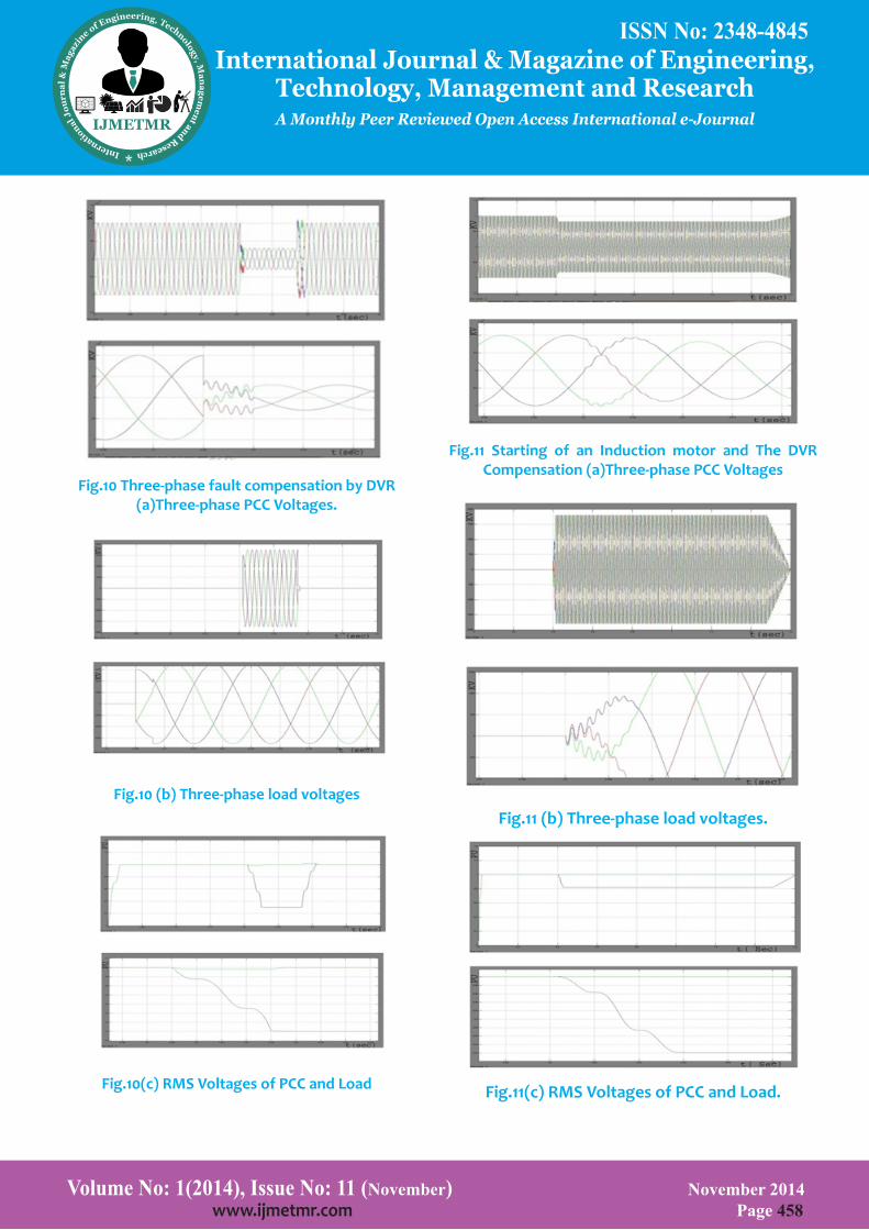
The DVR parameters and the control system specifica-tions are provided in Appendices A and B. At 205 ms, the fault is applied at 285 ms, and the breaker works and separates the line between buses transformer and breaker from the system. At 305 ms, the fault will be recovered and, finally, at 310 ms, the separated line will be rejoined to the system by the breaker. The simula-tion results are shown in Fig.10 As can be seen in the figure, the RMS voltage of PCC drops to about 0.25p.u. During the fault it is obvious that this remaining volt-age is due to the impedances in the system. The DVR will start the compensation just after the detection of sag. As can be seen in the enlarged figure, the DVR has restored the voltage to normal form with attenuation of the oscillations at the start of the compensation in less than half a cycle. It is worth noting that the amount and shape of the oscillations depends also on the time of applying the fault. As can be seen in the enlarged figure, the voltage value of phase B is nearly zero; this phase has minimum oscillation when the fault starts.
C. Starting the Induction Motor:
A large induction motor is started on bus transformer. The motor specifications are provided in Appendix C. The large motor starting current will cause the PCC voltage (bus transformer voltage) to drop. The simula-tion results in the case of using the DVR are shown in Fig.11 In this simulation, the motor is started at 405 ms. as can be seen in Fig.11, at this time, the PCC rms volt-age drops to about 0.8 p.u. The motor speed reaches the Nominal value in About 1s during this period, the PCC bus is under voltage sag. From 1.4 s, as the speed approaches nominal, the voltage also approaches the normal condition. However, during all of these events, the DVR keeps the load bus voltage (bus load voltage) at the normal condition. Also, as can be seen in the en-larged version of Fig.11, the DVR has succeeded in re-storing the load voltage in half a cycle from the instant of the motor starting.
D. Fault Current Limiting:
The last simulation is run for a symmetrical downstream fault, and the capability of the DVR to reduce the fault current and restore the PCC voltage is tested. For this purpose, a three-phase short circuit is applied on bus load. In Fig.12, the fault current, without the DVR com-pensation, is shown.
For the simulation with DVR compensation, the three-phase fault is applied at 205 ms and then removed af-ter 0.1 s. Also, a breaker will remove the faulted bus from the entire system at 300 ms. Fig.13 shows the DVR operation during the fault.
As can be seen, the rms obvious that this remaining voltage is due to the impedances in the system. The DVR will start the compensation just after the detec-tion of sag. As can be seen in the enlarged figure, the DVR has restored the voltage to normal form with at-tenuation of the oscillations at the start of the com-pensation in less than half a cycle.
It is worth noting that the amount and shape of the oscillations depends also on the time of applying the fault. As can be seen in the enlarged figure, the voltage value of phase B is nearly zero; this phase has minimum oscillation when the fault starts.
C. Starting the Induction Motor:
A large induction motor is started on bus transformer. The motor specifications are provided in Appendix C. The large motor starting current will cause the PCC voltage (bus transformer voltage) to drop.
The simulation results in the case of using the DVR are shown in Fig.11 In this simulation, the motor is started at 405 ms. as can be seen in Fig.11, at this time, the PCC rms voltage drops to about 0.8 p.u.
The motor speed reaches the Nominal value in load bus voltage reaches zero during the fault, and as the en-larged figure shows, in about half a cycle, the DVR has succeeded in restoring the PCC voltage wave shape to the normal condition.
It should be noted that the amount and shape of the oscillations depend on the time of applying the fault. As Fig.13 shows, at this time, the voltage value of phase B is nearly zero; this phase has the minimum oscillation when the fault starts.
Also, the maximum value of the fault current has been reduced from 40 kA (see Fig.12) to 5 kA with DVR com-pensation.
Volume No: 1(2014), Issue No: 11 (November) November 2014 www.ijmetmr.com Page 458
ISSN No: 2348-4845International Journal & Magazine of Engineering,
Technology, Management and ResearchA Monthly Peer Reviewed Open Access International e-Journal
Fig.10 Three-phase fault compensation by DVR(a)Three-phase PCC Voltages.
Fig.10 (b) Three-phase load voltages
Fig.10(c) RMS Voltages of PCC and Load
Fig.11 Starting of an Induction motor and The DVR Compensation (a)Three-phase PCC Voltages
Fig.11 (b) Three-phase load voltages.
Fig.11(c) RMS Voltages of PCC and Load.
Volume No: 1(2014), Issue No: 11 (November) November 2014 www.ijmetmr.com Page 457
ISSN No: 2348-4845International Journal & Magazine of Engineering,
Technology, Management and ResearchA Monthly Peer Reviewed Open Access International e-Journal
The DVR parameters and the control system specifica-tions are provided in Appendices A and B. At 205 ms, the fault is applied at 285 ms, and the breaker works and separates the line between buses transformer and breaker from the system. At 305 ms, the fault will be recovered and, finally, at 310 ms, the separated line will be rejoined to the system by the breaker. The simula-tion results are shown in Fig.10 As can be seen in the figure, the RMS voltage of PCC drops to about 0.25p.u. During the fault it is obvious that this remaining volt-age is due to the impedances in the system. The DVR will start the compensation just after the detection of sag. As can be seen in the enlarged figure, the DVR has restored the voltage to normal form with attenuation of the oscillations at the start of the compensation in less than half a cycle. It is worth noting that the amount and shape of the oscillations depends also on the time of applying the fault. As can be seen in the enlarged figure, the voltage value of phase B is nearly zero; this phase has minimum oscillation when the fault starts.
C. Starting the Induction Motor:
A large induction motor is started on bus transformer. The motor specifications are provided in Appendix C. The large motor starting current will cause the PCC voltage (bus transformer voltage) to drop. The simula-tion results in the case of using the DVR are shown in Fig.11 In this simulation, the motor is started at 405 ms. as can be seen in Fig.11, at this time, the PCC rms volt-age drops to about 0.8 p.u. The motor speed reaches the Nominal value in About 1s during this period, the PCC bus is under voltage sag. From 1.4 s, as the speed approaches nominal, the voltage also approaches the normal condition. However, during all of these events, the DVR keeps the load bus voltage (bus load voltage) at the normal condition. Also, as can be seen in the en-larged version of Fig.11, the DVR has succeeded in re-storing the load voltage in half a cycle from the instant of the motor starting.
D. Fault Current Limiting:
The last simulation is run for a symmetrical downstream fault, and the capability of the DVR to reduce the fault current and restore the PCC voltage is tested. For this purpose, a three-phase short circuit is applied on bus load. In Fig.12, the fault current, without the DVR com-pensation, is shown.
For the simulation with DVR compensation, the three-phase fault is applied at 205 ms and then removed af-ter 0.1 s. Also, a breaker will remove the faulted bus from the entire system at 300 ms. Fig.13 shows the DVR operation during the fault.
As can be seen, the rms obvious that this remaining voltage is due to the impedances in the system. The DVR will start the compensation just after the detec-tion of sag. As can be seen in the enlarged figure, the DVR has restored the voltage to normal form with at-tenuation of the oscillations at the start of the com-pensation in less than half a cycle.
It is worth noting that the amount and shape of the oscillations depends also on the time of applying the fault. As can be seen in the enlarged figure, the voltage value of phase B is nearly zero; this phase has minimum oscillation when the fault starts.
C. Starting the Induction Motor:
A large induction motor is started on bus transformer. The motor specifications are provided in Appendix C. The large motor starting current will cause the PCC voltage (bus transformer voltage) to drop.
The simulation results in the case of using the DVR are shown in Fig.11 In this simulation, the motor is started at 405 ms. as can be seen in Fig.11, at this time, the PCC rms voltage drops to about 0.8 p.u.
The motor speed reaches the Nominal value in load bus voltage reaches zero during the fault, and as the en-larged figure shows, in about half a cycle, the DVR has succeeded in restoring the PCC voltage wave shape to the normal condition.
It should be noted that the amount and shape of the oscillations depend on the time of applying the fault. As Fig.13 shows, at this time, the voltage value of phase B is nearly zero; this phase has the minimum oscillation when the fault starts.
Also, the maximum value of the fault current has been reduced from 40 kA (see Fig.12) to 5 kA with DVR com-pensation.
Volume No: 1(2014), Issue No: 11 (November) November 2014 www.ijmetmr.com Page 458
ISSN No: 2348-4845International Journal & Magazine of Engineering,
Technology, Management and ResearchA Monthly Peer Reviewed Open Access International e-Journal
Fig.10 Three-phase fault compensation by DVR(a)Three-phase PCC Voltages.
Fig.10 (b) Three-phase load voltages
Fig.10(c) RMS Voltages of PCC and Load
Fig.11 Starting of an Induction motor and The DVR Compensation (a)Three-phase PCC Voltages
Fig.11 (b) Three-phase load voltages.
Fig.11(c) RMS Voltages of PCC and Load.

Volume No: 1(2014), Issue No: 11 (November) November 2014 www.ijmetmr.com Page 459
ISSN No: 2348-4845International Journal & Magazine of Engineering,
Technology, Management and ResearchA Monthly Peer Reviewed Open Access International e-Journal
Fig.12 Current wave shapes due to three-phase short circuit fault without DVR compensation.
Fig.13 Fault current limiting by DVR (a)Three-phase PCC Voltages.
Fig.13 (b) Three-phase load voltages.
Fig.13(c) Three-phase currents.
Fig.11(d) RMS Voltages of PCC and Load
V.CONCLUSION:
In this paper, a multifunctional DVR is proposed, and a closed-loop control system is used for its control to im-prove the damping of the DVR response. Also, for fur-ther improving the transient response and eliminating the steady-state error, the Posicast and P+Resonant controllers are used. As the second function of this DVR, using the flux-charge model, the equipment is controlled so that it limits the downstream fault cur-rents and protects the PCC voltage during these faults by acting as a variable impedance.
The problem of absorbed active power is solved by entering an impedance just at the start of this kind of fault in parallel with the dc-link capacitor and the bat-tery being connected in series with a diode so that the power does not enter it. The simulation results verify the effectiveness and capability of the proposed DVR in compensating for the voltage sags caused by short circuits and the large induction motor starting and lim-iting the downstream fault currents and protecting the PCC voltage.
REFERENCES:
[1] J. A. Martinez and J. Martin-Arnedo, “Voltage sag studies in distribution networks- part II: Voltage sag as-sessment,” IEEE Trans. Power Del., vol. 21, no. 3, pp. 1679–1688, Jul. 2006.
[2] J. A. Martinez and J. M. Arnedo, “Voltage sag stud-ies in distribution networks- part I: System modeling,” IEEE Trans. Power Del., vol. 21, no. 3, pp. 338–345, Jul. 2006.
[3] P. Hcine and M. Khronen, “Voltage sag distribution caused by power system faults,” IEEE Trans. Power Syst., vol. 18, no. 4, pp. 1367–1373, Nov. 2003.
Volume No: 1(2014), Issue No: 11 (November) November 2014 www.ijmetmr.com Page 460
ISSN No: 2348-4845International Journal & Magazine of Engineering,
Technology, Management and ResearchA Monthly Peer Reviewed Open Access International e-Journal
[4] S. S. Choi, B. H. Li, and D. M. Vilathgamuwa, “Dy-namic voltage restoration with minimum energy injec-tion,” IEEE Trans. Power Syst., vol. 15, no. 1, pp. 51–57, Feb. 2000.
[5] C. Fitzer, M. Barnes, and P. Green, “Voltage sag de-tection technique for a dynamic voltage restore,” IEEE Trans. Ind. Appl., vol. 2, no. 1, pp. 203–212, Jan./Feb. 2004.
[6] C. Benachaiba and B. Ferdi, “Voltage quality im-provement using DVR,” Electt. Power Qual. Utilisation, Journal, vol. XIV, no. 1, 2008.
[7] D. M. Vilathgamuwa, H. M. Wijekoon, and S. S. Choi, “A novel technique to compensate voltage sags in mul-tiline distribution system-the interline dynamic voltage restorer,” IEEE Trans. Ind. Electron., vol. 53, no. 5, pp. 1603–1611, Oct. 2006.
[8] J. G. Nielsen, M. Newman, H. Nielsen, and F. Blaab-jerg, “Control and testing of a dynamic voltage restor-er (DVR) at medium voltage level,” IEEE Trans. Power Electron., vol. 19, no. 3, pp. 806–813, May 2004.
[9] M. J. Newman, D. G. Holmes, J. G. Nielsen, and F. Blaabjerg, “A dynamic voltage restorer (DVR) with se-lective harmonic compensation at medium voltage lev-el,” IEEE Trans. Ind. Appl., vol. 41, no. 6, pp. 1744–1753, Nov./Dec. 2005.
[10] A. K. Jindal, A. Ghosh, and A. Joshi, “Critical load bus voltage control using DVR under system frequency variation,” Elect. Power Syst. Res., vol. 78, no. 2, pp. 255–263, Feb. 2008.
[11] Y. W. Li, D. M. Vilathgamuwa, P. C. Loh, and F. Blaabjerg, “A dualfunctional medium voltage level DVR to limit downstream fault currents,” IEEE Trans. Power Electron., vol. 22, no. 4, pp. 1330–1340, Jul. 2007.
[12] P. C. Loh, D. M. Vilathgamuwa, S. K. Tang, and H. L. Long, “Multilevel dynamic voltage restorer,” IEEE Power Electron. Lett., vol. 2, no. 4, pp. 125–130, Dec. 2004.
[13] E. Babaei, M. Farhadi, and M. Sabahi, “Compen-sation of voltage disturbances in distribution systems using single-phase dynamic voltage restorer,” Elect. Power Syst. Res., Jul. 2010.
[14] C. N.-M. Ho and H. S.-H. Chung, “Implementation and performance evaluation of a fast dynamic control scheme for capacitor-supported interline DVR,” IEEE Trans Power Electron., vol. 25, no. 8, pp. 1975–1988, Aug. 2010.
[15] M. Vilathgamuwa, A. A. D. R. Perera, and S. S. Choi, “Performance improvement of the dynamic voltage re-storer with closed-loop load voltage and current-mode control,” IEEE Trans. Power Electron., vol. 17, no. 5, pp. 824–834, Sep. 2002.
[16] Y. W. Li, P. C. Loh, F. Blaabjerg, and D. M.Vilathgamuwa, “Investigation and improvement of transient response of DVR at medium voltage level,” IEEE Trans. Ind. Appl., vol. 43, no. 5, pp. 1309–1319, Sep./Oct. 2007.
[17] H. Kim and S. K. Sul, “Compensation voltage con-trol in dynamic voltage restorers by use of feedforward and state feedback scheme,” IEEE Trans. Power Elec-tron., vol. 20, no. 5, pp. 1169–1177, Sep. 2005.
[18] M. I. Marei, E. F. El-Saadany, and M. M. A. Salama, “A new approach to control DVR based on symmetrical components estimation,” IEEE Trans. Power Del., vol. 22, no. 4, pp. 2017–2024, Oct. 2007.
[19] Y. W. Li, D. M. Vilathgamuwa, F. Blaabjerg, and P. C. Loh, “A robust control scheme for medium-voltage-levelDVR implementation,” IEEE Trans. Ind. Electron., vol. 54, no. 4, pp. 2249–2261, Aug. 2007.
[20] S. A. Saleh, C. R. Moloney, and M. A. Rahman, “Im-plementation of a dynamic voltage restorer system based on discretewavelet transforms,” IEEE Trans. Power Del., vol. 23, no. 4, pp. 2360–2375, Oct. 2008.