Embed Size (px)
Citation preview

Zang et al. / Front Inform Technol Electron Eng 2020 21(4):604-614 604
A new approach for analyzing the effect of non-ideal power supply on a constant current underwater cabled system*
Yu-jia ZANG, Yan-hu CHEN†‡, Can-jun YANG, De-jun LI, Ze-jian CHEN, Gul MUHAMMAD The State Key Laboratory of Fluid Power and Mechatronic Systems, Zhejiang University, Hangzhou 310027, China
†E-mail: [email protected] Received Nov. 21, 2018; Revision accepted May 9, 2019; Crosschecked Feb. 19, 2020
Abstract: The effect of a constant current (CC) power supply on the CC ocean observation system is a problem that once was neglected. The dynamic characteristics of the CC power supply may have great influence on the whole system, especially the voltage behavior in the event of load change. This needs to be examined. In this paper, a method is introduced to check whether the CC power supply can satisfy the dynamic requirements of the CC ocean observation system. An equivalent model to describe the non-ideal CC power supply is presented, through which the dynamic characteristics can be standardized. To verify the feasibility of this model, a minimum system of a single node in the CC ocean observation system is constructed, from which the model is derived. Focusing on the power failure problem, the output voltage responses are performed and the models are validated. Through the model, the dynamic behavior of the CC power supply is checked in a practical design. Key words: Non-ideal power supply; Constant current input; Ocean observation system https://doi.org/10.1631/FITEE.1800737 CLC number: TP202 1 Introduction
An ocean observation system enables long-term, real-time, and in-situ observation of oceans. It plays an important role in ocean exploration and research (Chave et al., 2004). With constant voltage (CV) transmission (Taylor, 2008; Pawlak et al., 2009) and constant current (CC) transmission (Duennebier et al. 2002; Asakawa et al., 2003), direct current (DC) transmission has been applied widely in ocean ob-servation systems because of its low cost (Howe et al., 2002). In China, DC–CV transmission is used in the ocean observation system in the South China Sea
(Chen et al., 2012, 2013). However, compared with CV transmission, CC transmission has many advantages such as good robustness and ease in lo-cating the fault point and isolating underwater electric circuits (Asakawa et al., 2007). However, most sci-entific instruments are powered by CV. Hence, converting CC into CV is a functionality that the CC ocean observation system should possess.
Similarly, commercial submarine communication systems are usually powered by CC. Both the repeater and the branch unit (BU) adopt the CC input to con-nect directly and to collect electricity from a subma-rine cable (Takehira, 2016). However, similar to the repeater and BU, an ocean observation system also has terminal nodes such as the junction box and the science instrument interface module (Howe et al., 2011; Qu et al., 2015). Unlike commercial submarine communication systems, the load power of ocean observation systems may change frequently because of the possible cut-in and cut-out of scientific in-struments (Chen et al., 2012). When designing a ter-minal node prototype in a CC ocean observation
Frontiers of Information Technology & Electronic Engineering www.jzus.zju.edu.cn; engineering.cae.cn; www.springerlink.com ISSN 2095-9184 (print); ISSN 2095-9230 (online) E-mail: [email protected]
‡ Corresponding author * Project supported by the National Natural Science Foundation of China (No. 41676089), the Natural Science Foundation of Zhejiang Province, China (No. LY18E090003), and the Fundamental Research Funds for the Central Universities, China (No. 2018QNA4005)
ORCID: Yu-jia ZANG, https://orcid.org/0000-0002-2712-9854; Yan-hu CHEN, https://orcid.org/0000-0002-5020-7355 © Zhejiang University and Springer-Verlag GmbH Germany, part of Springer Nature 2020
Zang et al. / Front Inform Technol Electron Eng 2020 21(4):604-614 605
system, we found that when an external load cuts in, the system output voltage drops rapidly and recovers after a while. As a rule of thumb, because of the power supply, using CC transmission may increase the re-sponse time of the output voltage with load change, and may change the magnitude of voltage fluctuation. In a current distribution system, CC power supply is often regarded as an ideal CC source (Wang HJ et al., 2017b), although such a simplified method may lead to large errors. However, the ocean observation sys-tem has to be ultra-reliable (Petitt et al., 2002). Therefore, the effect of CC power supply is nonnegligible and it is necessary to know the dynamic performance of voltage in the event of load change. There are various types of CC power supplies with different topologies and control strategies (Lour-dusami and Vairamani, 2014; Qu et al., 2015; Wang ZY et al., 2017). In addition, the internal structures of most “off-the-shelf” power supplies are unknown and are essentially “black boxes.” We need to find a method to describe the dynamic performance of these “black boxes,” so that we can analyze their effects on the dynamic characteristics of the device in parallel, and the CC power supply can be checked before being applied in practice. Hence, an equivalent dynamic model of non-ideal CC power supply needs to be proposed and analyzed.
To study the effect of power supply, a minimum system of a single node in a CC ocean observation system that can convert CC into CV must be con-structed and modeled. Converting CC into CV de-mands closed-loop control. However, CC systems are fundamentally and unconditionally unstable with the standard regulated method (Harris and Duennebier, 2002). Fortunately, the problem can be overcome by a shunt regulator which can realize CV output and make the CC system stable (Duennebier et al., 2002; Harris and Duennebier, 2002). Such a method is used widely in ocean observation systems such as HUGO (Duennebier et al., 2002), H2O (Petitt et al., 2002), and ACO (Howe et al., 2011). The converter is an-other necessary component in an ocean observation system. It can enlarge or reduce the input voltage (or the current for a CC input) by a certain ratio. The characteristics of a converter working with CC inputs are quite different from those of one working with CV inputs (Wang HJ et al., 2017a). A push–pull converter used for a CC ocean observation system was proposed
by Asakawa et al. (2003). Similar push–pull con-verters have been studied well and applied widely in many fields (Lai et al., 1992; Cruz et al., 2004; Tru-jillo et al., 2011); however, these studies focused on the circumstances with CV inputs. Furthermore, literature on the dynamic model of the minimum system is scarce. Hence, the dynamic model of the push–pull converter with CC input and the model of the shunt regulator need to be derived, so that the model of the minimum system can be obtained.
In this paper, the main goal is to find a method describing the dynamic behavior of a CC power sup-ply, so that we can check whether the CC power sup-ply can meet the engineering requirements of a CC ocean observation system. The method for analyzing the effect of CC power supply is presented by com-bining a minimum system within a CC ocean obser-vation system. In this paper, the minimum system consists of a push–pull converter, a shunt regulator, and an external load.
2 Non-ideal constant current power supply model
The average-value model and small signal model
are used widely in many fields (Tannir et al., 2016; Alonge et al., 2017; Florez-Tapia et al., 2017; Huang and Abu Qahouq, 2017; Zhang et al., 2017), and also used in this study. To use the small signal model, we need to separate some variables into the following form:
ˆ,a A a= + (1)
where A represents the steady value and a represents the small signal value.
2.1 Equivalent model of constant current power supply
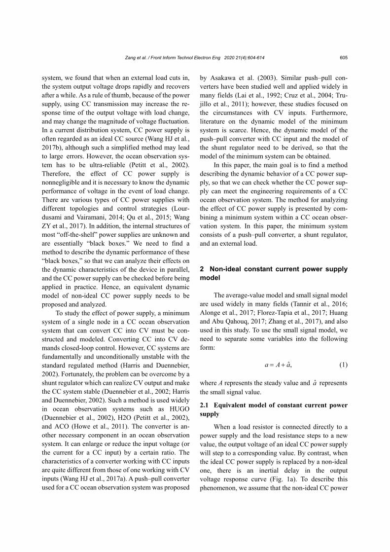
When a load resistor is connected directly to a power supply and the load resistance steps to a new value, the output voltage of an ideal CC power supply will step to a corresponding value. By contrast, when the ideal CC power supply is replaced by a non-ideal one, there is an inertial delay in the output voltage response curve (Fig. 1a). To describe this phenomenon, we assume that the non-ideal CC power
Zang et al. / Front Inform Technol Electron Eng 2020 21(4):604-614 606
supply consists of an ideal CC source in parallel with an equivalent admittance g with the following dy-namic requirements (Fig. 1b):
1. When the load resistance steps to a higher (or lower) value, it can act as a buffer against the sudden change of the output voltage. Then it can be dis-charged (or charged) so that the output voltage can increase (or decrease) slowly.
2. After a while, the current flowing through the equivalent admittance g is equal to 0, namely, having negligible or even no effect on the steady state of the output voltage.
3. The output voltage curve is required to fit ap-propriately with the actual non-ideal power supply.
If it is a capacitor in parallel with the ideal CC source, the first two requirements are satisfied. The current flowing through a capacitor is the multiplica-tion of the derivative of its voltage with respect to time and its own capacitance C. The admittance of capacitor C can be written as
d ,dCg Ct
= (2)
where d/dt represents a derivative operator with re-spect to time. Nonetheless, it is difficult to fit appro-priately with an actual non-ideal power supply.
Therefore, based on Eq. (2), g is constructed in the following form:
1
1 01
d d ,d d
n n
n nn ng A A At t
−
− −= + + + (3)
where Ai (n=0, 1, …, n) are parameters that can be determined in system identification. A0 should be fairly small. Thus, the current flowing through g can be obtained by
1s s
s 1 0 s1
d d.
d d
n n
g n nn n
v vi gv A A A vt t
−
− −= = + + + (4)
When the output voltage becomes steady (vss),
the derivatives and higher-order derivatives of the output voltage are equal to zero, and A0 is small enough to be ignored. Then we can obtain
1
ss ss_steady ss 1 0 ss1
d d0.
d d
n n
g n nn n
v vi gv A A A vt t
−
− −= = + + + =
(5)
In other words, the steady-state current of g is equal to zero. Hence, g will not affect the steady state of the output voltage. This is consistent with condi- tion 2.
With zero initial values, by applying a Laplace transform, we can obtain
s( ) ( ) ( ),I s G s V s= (6)
where
11 0( ) .n n
n nG s A s A s A−−= + + + (7)
2.2 Method for obtaining G(s)
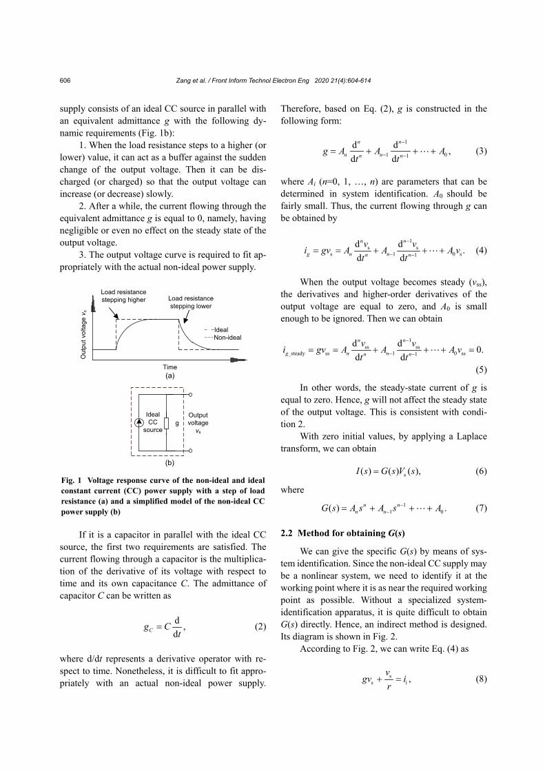
We can give the specific G(s) by means of sys-tem identification. Since the non-ideal CC supply may be a nonlinear system, we need to identify it at the working point where it is as near the required working point as possible. Without a specialized system- identification apparatus, it is quite difficult to obtain G(s) directly. Hence, an indirect method is designed. Its diagram is shown in Fig. 2.
According to Fig. 2, we can write Eq. (4) as
ss i ,
vgv i
r+ = (8)
Out
put v
olta
ge v
s
Load resistance stepping higher
– – Ideal––– Non-ideal
Load resistance stepping lower
Time
IdealCC
sourceg
Output voltage
vs
(a)
(b)
Fig. 1 Voltage response curve of the non-ideal and ideal constant current (CC) power supply with a step of load resistance (a) and a simplified model of the non-ideal CC power supply (b)
Zang et al. / Front Inform Technol Electron Eng 2020 21(4):604-614 607
where vs and r represent the output voltage of the power supply and load resistance, respectively, and ii
is the output current from the ideal CC source. We separate variables into the form of Eq. (1):
s s s
i i
ˆ ,ˆ,
.
= + = + =
v V vr R ri I
(9)
Taking Eq. (9) into Eq. (8), let A0 be sufficiently
small, and ignore the second-order small signal. Then with a Laplace transform, we can obtain
i ( )( ) ,( )
I H sG sH s−
= (10)
where s ( )
( ) .ˆ( )
v sH sr s
= (11)
In the experiment, we assume that the steady
input resistance of the converter above is equal to R+ΔR. Then we select two resistors with resistance values R and ΔR, respectively. Therefore, using switch K, we can let resistance r step from R to R+ΔR, and record the output voltage response curve. Then H(s) can be obtained through system identification. Finally, we can obtain G(s) from Eq. (10).
However, Eq. (10) is derived from the small signal model. On one hand, if ΔR cannot be small enough, it may cause a relatively large error. On the other hand, in the actual experiment, it requires a relatively large value of ΔR to obtain a clear voltage response curve. Hence, an adjustment method is needed. Through our previous experiments, results
would be better if we add a correction factor α to Eq. (10):
i ( )
( ) .( )α
I H sG s α
H s−
= (12)
The physical meaning of α adjustment is obvious:
if n=1 and A0=0, G(s)=A1s. A1 can be seen as the ca-pacitance of a capacitor. The value obtained by sys-tem identification may be different from the actual value. We further adjust α as the capacitance value through other experiments. Similarly, if n>1, for en-gineering convenience, α is, in fact, an overall ampli-fication or reduction of all the coefficients in G(s). An example including α adjustment for obtaining Gα(s) is presented in Section 4.
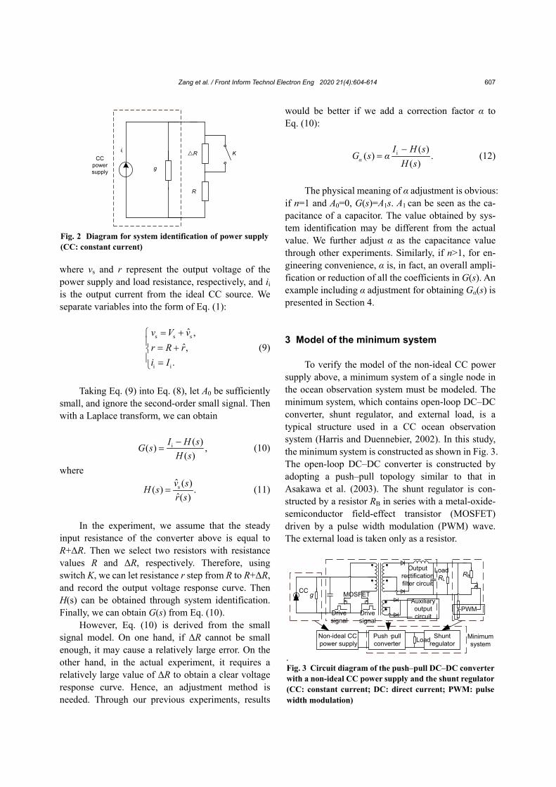
3 Model of the minimum system
To verify the model of the non-ideal CC power supply above, a minimum system of a single node in the ocean observation system must be modeled. The minimum system, which contains open-loop DC–DC converter, shunt regulator, and external load, is a typical structure used in a CC ocean observation system (Harris and Duennebier, 2002). In this study, the minimum system is constructed as shown in Fig. 3. The open-loop DC–DC converter is constructed by adopting a push–pull topology similar to that in Asakawa et al. (2003). The shunt regulator is con-structed by a resistor RB in series with a metal-oxide- semiconductor field-effect transistor (MOSFET) driven by a pulse width modulation (PWM) wave. The external load is taken only as a resistor.
Non-ideal CC power supply
Push–pullconverter
Shunt regulator
Auxiliaryoutputcircuit
PWM
Outputrectificationfilter circuit
LoadRL
RB
Drive signal
Drive signal
MOSFETCC g
Minimumsystem
Load
. Fig. 3 Circuit diagram of the push–pull DC–DC converter with a non-ideal CC power supply and the shunt regulator (CC: constant current; DC: direct current; PWM: pulse width modulation)
CCpowersupply g
△R
R
Kii
Fig. 2 Diagram for system identification of power supply (CC: constant current)
Zang et al. / Front Inform Technol Electron Eng 2020 21(4):604-614 608
3.1 Model of the converter
The model of this converter is derived under the following assumptions:
1. The converter works in the continuous con-duction mode (CCM).
2. All the components are assumed to be ideal, except for diodes and MOSFETs.
Detailed derivation can be found in the appendix. Note that n1 is the ratio between turns of the main output side and the primary side, n2 is the ratio be-tween turns of the auxiliary output side and the pri-mary side, ii, iL, and ia are the input current, the current flowing through inductance L, and the current of the auxiliary output circuit, respectively, VDS and VD are drop voltages of MOSFET and the diode, respectively, vci and vo are voltages of Ci and Co, respectively, and d is the nominal duty cycle of the converter. These variables satisfy Eq. (1).
Through the small signal model, we can obtain the steady state as
io 1 o i D
2 1
( ) ,αc G
II DV n R V V VD n n
= − = − −
(13)
2 D 1i 1 o DS2
2
,g αc
I I v nV n R vD n D D
= − + +
(14)
i
1 2
.αL II ID n n= + (15)
The transfer function from the small signal of the
load and the small signal of the output voltage is
o
o
ˆ ( ) ( ) ,ˆ ( ) ( )v s N sr s D s
= (16)
where 21
12( ) ( ( )) ,L LnN s I L C s G s ID
= + +
2 221 1
2 o 1 12 2
21
1 o 2 o2
( ) ( ( )) ( ( ))
( ( )) 1.
= + + +
+ + + +
n nD s Lc R s C s G s Ls C s G sD D
n C s G s R C R sD
3.2 Model of the shunt regulator
The shunt regulator is equivalent to a variable resistor which can be controlled by a controller. The
resistance of the shunt regulator and the resistance of the load are equivalent to a resistance ro. With a con-troller, ro can converge to a steady value. In other words, the output voltage can converge to a steady value. As shown in Fig. 3, when duty cycle dB changes, the current of RB would flow discontinuously, so as to lead to variability of the equivalent resistance of the shunt regulator (rB). The equivalent resistance of the shunt regulator and the load is equal to ro.
We can obtain the small signal model of the equivalent resistance of the shunt regulator and the load as
Bo
B B
,L
L
R RR
D R R=
+ (17)
B
o BB B
ˆˆ ( ) ( ),L
L
R Rr s d s
D R R=
+ (18)
B s oo B
B B
/ˆ ˆ( ) ( )./L
R D Rr s r s
R R D−
=+
(19)
From Eqs. (18) and (19), under the small signal
model, the increment of ro is equal to the increment of dB multiplied by a negative gain plus the increment of rB multiplied by a positive gain.
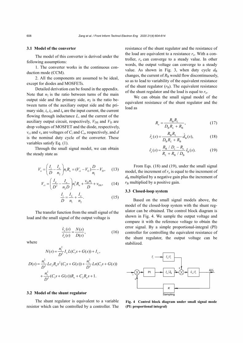
3.3 Closed-loop system
Based on the small signal models above, the model of the closed-loop system with the shunt reg-ulator can be obtained. The control block diagram is shown in Fig. 4. We sample the output voltage and compare it with the reference voltage to obtain the error signal. By a simple proportional-integral (PI) controller for controlling the equivalent resistance of the shunt regulator, the output voltage can be stabilized.
ΔVo
o Lr rLr
o Bˆr d o ˆˆ Lv rPI
K
Sampling
+−
++
Fig. 4 Control block diagram under small signal mode (PI: proportional integral)
Zang et al. / Front Inform Technol Electron Eng 2020 21(4):604-614 609
4 Experimental verification and discussions
4.1 Obtaining the model of constant current power supply
4.1.1 Obtaining G(s)
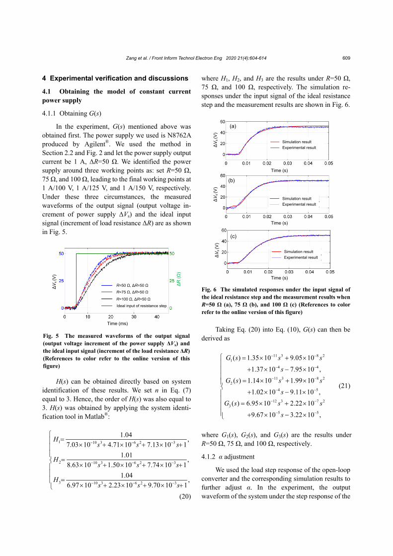
In the experiment, G(s) mentioned above was obtained first. The power supply we used is N8762A produced by Agilent®. We used the method in Section 2.2 and Fig. 2 and let the power supply output current be 1 A, ΔR=50 Ω. We identified the power supply around three working points as: set R=50 Ω, 75 Ω, and 100 Ω, leading to the final working points at 1 A/100 V, 1 A/125 V, and 1 A/150 V, respectively. Under these three circumstances, the measured waveforms of the output signal (output voltage in-crement of power supply ΔVs) and the ideal input signal (increment of load resistance ΔR) are as shown in Fig. 5.
H(s) can be obtained directly based on system identification of these results. We set n in Eq. (7) equal to 3. Hence, the order of H(s) was also equal to 3. H(s) was obtained by applying the system identi-fication tool in Matlab®:
1 10 3 6 2 3
2 10 3 6 2 3
3 10 3 6 2 3
1.04 ,7.03 10 4.71 10 7.13 10 1
1.01 ,8.63 10 1.50 10 7.74 10 1
1.04 ,6.97 10 2.23 10 9.70 10 1
− − −
− − −
− − −
= × + × + × +
=
× + × + × +
=× + × + × +
Hs s s
Hs s s
Hs s s
(20)
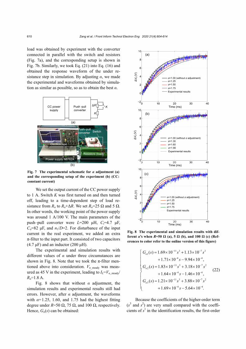
where H1, H2, and H3 are the results under R=50 Ω, 75 Ω, and 100 Ω, respectively. The simulation re-sponses under the input signal of the ideal resistance step and the measurement results are shown in Fig. 6.
Taking Eq. (20) into Eq. (10), G(s) can then be derived as
11 3 8 2
14 4
11 3 8 22
4 5
12 3 7 23
5 5
( ) 1.35 10 9.05 10
1.37 10 7.95 10 ,( ) 1.14 10 1.99 10
1.02 10 9.11 10 ,( ) 6.95 10 2.22 10
9.67 10 3.22 10 ,
− −
− −
− −
− −
− −
− −
= × + ×
+ × − × = × + ×
+ × − × = × + × + × − ×
G s s ss
G s s ss
G s s s
s
(21)
where G1(s), G2(s), and G3(s) are the results under R=50 Ω, 75 Ω, and 100 Ω, respectively.
4.1.2 α adjustment
We used the load step response of the open-loop converter and the corresponding simulation results to further adjust α. In the experiment, the output waveform of the system under the step response of the
ΔR
(Ω)
Time (ms)
ΔV
s (V
)
R=75 Ω, ΔR=50 Ω
R=100 Ω, ΔR=50 Ω
R=50 Ω, ΔR=50 Ω
Ideal input of resistance step
Fig. 5 The measured waveforms of the output signal (output voltage increment of the power supply ΔVs) and the ideal input signal (increment of the load resistance ΔR) (References to color refer to the online version of this figure)
ΔV
s (V
)
Simulation resultExperimental result
(a)
ΔV
s (V
)
Simulation resultExperimental result
(b)
ΔV
s (V
)
Time (s)
Simulation resultExperimental result
(c)
Time (s)
Time (s)
Fig. 6 The simulated responses under the input signal of the ideal resistance step and the measurement results when R=50 Ω (a), 75 Ω (b), and 100 Ω (c) (References to color refer to the online version of this figure)
Zang et al. / Front Inform Technol Electron Eng 2020 21(4):604-614 610
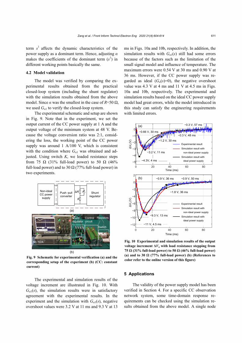
load was obtained by experiment with the converter connected in parallel with the switch and resistors (Fig. 7a), and the corresponding setup is shown in Fig. 7b. Similarly, we took Eq. (21) into Eq. (16) and obtained the response waveform of the under re-sistance step in simulation. By adjusting α, we made the experimental and waveforms obtained by simula-tion as similar as possible, so as to obtain the best α.
We set the output current of the CC power supply to 1 A. Switch K was first turned on and then turned off, leading to a time-dependent step of load re-sistance from Ro to Ro+ΔR. We set Ro=25 Ω and 5 Ω. In other words, the working point of the power supply was around 1 A/100 V. The main parameters of the push–pull converter were L=200 μH, Ci=4.7 μF, Co=82 μF, and n1/D=2. For disturbance of the input current in the real experiment, we added an extra π-filter to the input part. It consisted of two capacitors (4.7 μF) and an inductor (200 μH).
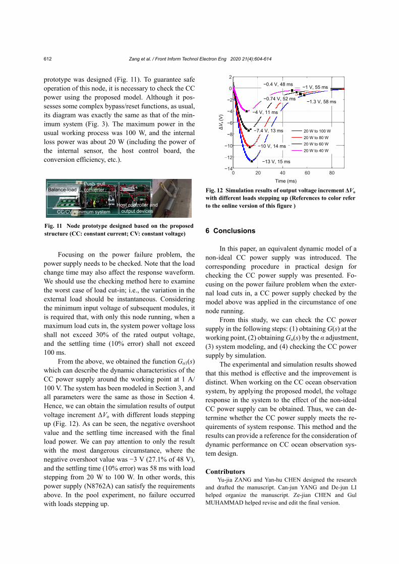
The experimental and simulation results with different values of α under three circumstances are shown in Fig. 8. Note that we took the π-filter men-tioned above into consideration. Vo_steady was meas-ured as 45 V in the experiment, leading to IL=Vo_steady/ Ro=1.8 A.
Fig. 8 shows that without α adjustment, the simulation results and experimental results still had errors. However, after α adjustment, the waveforms with α=1.25, 1.60, and 1.75 had the highest fitting degree under R=50 Ω, 75 Ω, and 100 Ω, respectively. Hence, Gα(s) can be obtained:
11 3 7 2
1
4 4
11 3 7 22
4 4
11 3 7 23
4 4
( ) 1.69 10 1.13 10
1.71 10 9.94 10 ,( ) 1.83 10 3.18 10
1.64 10 1.46 10 ,( ) 1.21 10 3.88 10
1.69 10 5.64 10 .
− −
− −
− −
− −
− −
− −
= × + ×
+ × − ×
= × + ×
+ × − ×
= × + ×
+ × − ×
α
α
α
G s s s
sG s s s
sG s s s
s
(22)
Because the coefficients of the higher-order term (s3 and s2) are very small compared with the coeffi-cients of s1 in the identification results, the first-order
Push–pullconverter
CC powersupply
ΔR
R
(a)
(b)
Push–pull converter Switch
Oscilloscope
Power supply N8762A
Resistors (load)
K
Fig. 7 The experimental schematic for α adjustment (a) and the corresponding setup of the experiment (b) (CC: constant current)
ΔV
s (V
)
Time (ms)
α=1.00 (without α adjustment)α=1.25α=1.50
Experimental results
(a)
ΔV
s (V
)α=1.00 (without α adjustment)α=1.30α=1.60α=1.90Experimental results
(b)
ΔV
s (V
)
Time (ms)
α=1.00 (without α adjustment)α=1.25α=1.50α=1.75Experimental results
(c)
Time (ms)
−2
−2
−2
α=1.75
Fig. 8 The experimental and simulation results with dif-ferent α’s when R=50 Ω (a), 5 Ω (b), and 100 Ω (c) (Ref-erences to color refer to the online version of this figure)
Zang et al. / Front Inform Technol Electron Eng 2020 21(4):604-614 611
term s1 affects the dynamic characteristics of the power supply as a dominant term. Hence, adjusting α makes the coefficients of the dominant term (s1) in different working points basically the same.
4.2 Model validation
The model was verified by comparing the ex-perimental results obtained from the practical closed-loop system (including the shunt regulator) with the simulation results obtained from the above model. Since α was the smallest in the case of R=50 Ω, we used Gα1 to verify the closed-loop system.
The experimental schematic and setup are shown in Fig. 9. Note that in the experiment, we set the output current of the CC power supply at 1 A and the output voltage of the minimum system at 48 V. Be-cause the voltage conversion ratio was 2:1, consid-ering the loss, the working point of the CC power supply was around 1 A/100 V, which is consistent with the condition where Gα1 was obtained and ad-justed. Using switch K, we loaded resistance steps from 75 Ω (31% full-load power) to 50 Ω (46% full-load power) and to 30 Ω (77% full-load power) in two experiments.
The experimental and simulation results of the voltage increment are illustrated in Fig. 10. With Gα1(s), the simulation results were in satisfactory agreement with the experimental results. In the experiment and the simulation with Gα1(s), negative overshoot values were 3.2 V at 11 ms and 9.3 V at 13
ms in Figs. 10a and 10b, respectively. In addition, the simulation results with Gα1(s) still had some errors because of the factors such as the limitation of the small signal model and influence of temperature. The maximum errors were 0.54 V at 30 ms and 0.90 V at 36 ms. However, if the CC power supply was re-garded as ideal (Gα(s)=0), the negative overshoot value was 4.3 V at 4 ms and 11 V at 4.5 ms in Figs. 10a and 10b, respectively. The experimental and simulation results based on the ideal CC power supply model had great errors, while the model introduced in this study can satisfy the engineering requirements with limited errors.
5 Applications
The validity of the power supply model has been
verified in Section 4. For a specific CC observation network system, some time-domain response re-quirements can be checked using the simulation re-sults obtained from the above model. A single node
(b)
(a)
Open-loop converter
Push–pull converter
Non-idealCC power
supply
Shuntregulator
ΔR
R
K
Shuntregulator
Control circuit
Resistors
Switch
Oscilloscope
N8762A
Fig. 9 Schematic for experimental verification (a) and the corresponding setup of the experiment (b) (CC: constant current)
−12
−10
−8
−6
−4
−2
0
2
0 20 40 60 80−5
−4
−3
−2
−1
0Δ
Vs (V
)
Time (ms)
ΔV
s (V
)(a)
−0.66 V, 30 ms
−1.2 V, 30 ms
−3.2 V, 11 ms
−4.3V, 4 ms
−0.3 V, 48 ms
−0.3 V, 57 ms
−0.9 V, 36 ms
−1.8 V, 36 ms
−0.9 V, 50 ms
−9.3 V, 13 ms
−11 V, 4.5 ms
(b)
ideal power supplySimulation result with
Simulation result with non-ideal power supply
Experimental result
ideal power supplySimulation result with
Simulation result with non-ideal power supply
Experimental result
0 20 40 60 80
Time (ms)
Fig. 10 Experimental and simulation results of the output voltage increment ΔVo with load resistance stepping from 75 Ω (31% full-load power) to 50 Ω (46% full-load power) (a) and to 30 Ω (77% full-load power) (b) (References to color refer to the online version of this figure)
Zang et al. / Front Inform Technol Electron Eng 2020 21(4):604-614 612
prototype was designed (Fig. 11). To guarantee safe operation of this node, it is necessary to check the CC power using the proposed model. Although it pos-sesses some complex bypass/reset functions, as usual, its diagram was exactly the same as that of the min-imum system (Fig. 3). The maximum power in the usual working process was 100 W, and the internal loss power was about 20 W (including the power of the internal sensor, the host control board, the conversion efficiency, etc.).
Focusing on the power failure problem, the power supply needs to be checked. Note that the load change time may also affect the response waveform. We should use the checking method here to examine the worst case of load cut-in; i.e., the variation in the external load should be instantaneous. Considering the minimum input voltage of subsequent modules, it is required that, with only this node running, when a maximum load cuts in, the system power voltage loss shall not exceed 30% of the rated output voltage, and the settling time (10% error) shall not exceed 100 ms.
From the above, we obtained the function Gα1(s) which can describe the dynamic characteristics of the CC power supply around the working point at 1 A/ 100 V. The system has been modeled in Section 3, and all parameters were the same as those in Section 4. Hence, we can obtain the simulation results of output voltage increment ΔVo with different loads stepping up (Fig. 12). As can be seen, the negative overshoot value and the settling time increased with the final load power. We can pay attention to only the result with the most dangerous circumstance, where the negative overshoot value was −3 V (27.1% of 48 V), and the settling time (10% error) was 58 ms with load stepping from 20 W to 100 W. In other words, this power supply (N8762A) can satisfy the requirements above. In the pool experiment, no failure occurred with loads stepping up.
6 Conclusions
In this paper, an equivalent dynamic model of a
non-ideal CC power supply was introduced. The corresponding procedure in practical design for checking the CC power supply was presented. Fo-cusing on the power failure problem when the exter-nal load cuts in, a CC power supply checked by the model above was applied in the circumstance of one node running.
From this study, we can check the CC power supply in the following steps: (1) obtaining G(s) at the working point, (2) obtaining Gα(s) by the α adjustment, (3) system modeling, and (4) checking the CC power supply by simulation.
The experimental and simulation results showed that this method is effective and the improvement is distinct. When working on the CC ocean observation system, by applying the proposed model, the voltage response in the system to the effect of the non-ideal CC power supply can be obtained. Thus, we can de-termine whether the CC power supply meets the re-quirements of system response. This method and the results can provide a reference for the consideration of dynamic performance on CC ocean observation sys-tem design.
Contributors
Yu-jia ZANG and Yan-hu CHEN designed the research and drafted the manuscript. Can-jun YANG and De-jun LI helped organize the manuscript. Ze-jian CHEN and Gul MUHAMMAD helped revise and edit the final version.
Balance-loadPush–pull converter
CC/CV minimum systemHost controller and
output devices
Fig. 11 Node prototype designed based on the proposed structure (CC: constant current; CV: constant voltage)
0 20 40 60 80−14
−8
−6
−4
−2
0
2
20 W to 100 W20 W to 80 W20 W to 60 W20 W to 40 W
ΔV
s (V
)
Time (ms)
−0.4 V, 48 ms −1 V, 55 ms
−0.74 V, 52 ms −1.3 V, 58 ms
−4 V, 11 ms
−7.4 V, 13 ms
−10 V, 14 ms
−13 V, 15 ms−12
−10
Fig. 12 Simulation results of output voltage increment ΔVo with different loads stepping up (References to color refer to the online version of this figure )

Zang et al. / Front Inform Technol Electron Eng 2020 21(4):604-614 613
Acknowledgements The authors would like to thank Mei-yan PAN and Joce-
lyn M. LOSH for their help with this paper. Compliance with ethics guidelines
Yu-jia ZANG, Yan-hu CHEN, Can-jun YANG, De-jun LI, Ze-jian CHEN, and Gul MUHAMMAD declare that they have no conflict of interest.
References Alonge F, Pucci M, Rabbeni R, et al., 2017. Dynamic
modelling of a quadratic DC/DC single-switch boost converter. Electr Power Syst Res, 152:130-139.
https://doi.org/10.1016/j.epsr.2017.07.008 Asakawa K, Kojima J, Muramatsu J, et al., 2003. Novel current
to current converter for mesh-like scientific underwater cable network-concept and preliminary test result. Proc Oceans. Celebrating the Past ... Teaming Toward the Future, p.1868-1873.
https://doi.org/10.1109/OCEANS.2003.178172 Asakawa K, Kojima J, Muramatsu J, et al., 2007. Current-
to-current converter for scientific underwater cable networks. IEEE J Ocean Eng, 32(3):584-592.
https://doi.org/10.1109/JOE.2007.905024 Chave AD, Waterworth G, Maffei AR, et al., 2004. Cabled
ocean observatory systems. Mar Technol Soc J, 38(2): 30-43. https://doi.org/10.4031/002533204787522785
Chen YH, Yang CJ, Li DJ, et al., 2012. Design and application of a junction box for cabled ocean observatories. Mar Technol Soc J, 46(3):50-63.
https://doi.org/10.4031/MTSJ.46.3.4 Chen YH, Yang CJ, Li DJ, et al., 2013. Study on 10 KVDC
powered junction box for a cabled ocean observatory system. China Ocean Eng, 27(2):265-275.
https://doi.org/10.1007/s13344-013-0023-y Cruz J, Castilla M, Miret J, et al., 2004. Averaged large-signal
model of single magnetic push-pull forward converter with built-in input filter. Proc IEEE Int Symp on Industrial Electronics, p.1023-1028.
https://doi.org/10.1109/ISIE.2004.1571954 Duennebier FK, Harris DW, Jolly J, et al., 2002. Hugo: the
Hawaii undersea geo-observatory. IEEE J Ocean Eng, 27 (2):218-227. https://doi.org/10.1109/JOE.2002.1002476
Florez-Tapia AM, Ibanez FM, Vadillo J, et al., 2017. Small signal modeling and transient analysis of a trans quasi-Z-source inverter. Electric Power Syst Res, 144:52-62. https://doi.org/10.1016/j.epsr.2016.10.066
Harris DW, Duennebier FK, 2002. Powering cabled ocean- bottom observatories. IEEE J Ocean Eng, 27(2): 202-211. https://doi.org/10.1109/JOE.2002.1002474
Howe BM, Kirkham H, Vorpérian V, 2002. Power system considerations for undersea observatories. IEEE J Ocean Eng, 27(2):267-274.
https://doi.org/10.1109/JOE.2002.1002481 Howe BM, Lukas R, Duennebier F, et al., 2011. ALOHA
cabled observatory installation. Proc Oceans MTS/ IEEE KONA, p.1-11.
https://doi.org/10.23919/oceans.2011.6107301 Huang WX, Abu Qahouq JA, 2017. Small-signal modeling and
controller design of energy sharing controlled distributed battery system. Simul Model Pract Theory, 77:1-19.
https://doi.org/10.1016/j.simpat.2017.05.001 Lai RS, Ngo KDT, Watson JK, 1992. Steady-state analysis of
the symmetrical push-pull power converter employing a matrix transformer. IEEE Trans Power Electron, 7(1):44-53. https://doi.org/10.1109/63.124576
Lourdusami SS, Vairamani R, 2014. Analysis, design and experimentation of series-parallel LCC resonant converter for constant current source. IEICE Electr Expr, 11(17):20140711.
https://doi.org/10.1587/elex.11.20140711 Pawlak G, de Carlo EH, Fram JP, et al., 2009. Development,
deployment, and operation of Kilo Nalu nearshore cabled observatory. Proc OCEANS-EUROPE, p.1-10.
https://doi.org/10.1109/OCEANSE.2009.5278149 Petitt RA, Harris DW, Wooding B, et al., 2002. The Hawaii-2
observatory. IEEE J Ocean Eng, 27(2):245-253. https://doi.org/10.1109/JOE.2002.1002479 Qu FZ, Wang ZD, Song H, et al., 2015a. A study on a cabled
seafloor observatory. IEEE Intell Syst, 30(1):66-69. https://doi.org/10.1109/MIS.2015.9 Takehira K, 2016. Submarine system powering. In: Chesnoy J
(Ed.), Undersea Fiber Communication Systems (2nd Ed.). Academic Press, London, p.381-402.
https://doi.org/10.1016/B978-0-12-804269-4.00010-6 Tannir D, Wang Y, Li P, 2016. Accurate modeling of nonideal
low-power PWM DC–DC converters operating in CCM and DCM using enhanced circuit-averaging techniques. ACM Trans Des Autom ElectrSyst, 21(4):61.
https://doi.org/10.1145/2890500 Taylor SM, 2008. Supporting the operations of the NEPTUNE
Canada and VENUS cabled ocean observatories. Proc OCEANS MTS/IEEE Kobe Techno-Ocean, p.1-8.
https://doi.org/10.1109/OCEANSKOBE.2008.4530975 Trujillo CL, Velasco D, Figueres E, et al., 2011. Modeling and
control of a push-pull converter for photovoltaic microinverters operating in island mode. Appl Energy, 88(8):2824-2834. https://doi.org/10.1016/j.apenergy.2011.01.053
Wang HJ, Saha T, Zane R, 2017a. Analysis and design of a series resonant converter with constant current input and regulated output current. Proc IEEE Applied Power Electronics Conf and Exposition, p.1741-1747.
https://doi.org/10.1109/APEC.2017.7930934 Wang HJ, Saha T, Zane R, 2017b. Impedance-based stability
analysis and design considerations for DC current distribution with long transmission cable. Proc IEEE Workshop on Control and Modeling for Power Electronics, p.1-8.
https://doi.org/10.1109/COMPEL.2017.8013355 Wang ZY, Lai XQ, Wu Q, 2017. A PSR CC/CV flyback
converter with accurate CC control and optimized CV regulation strategy. IEEE Trans Power Electron, 32(9): 7045-7055. https://doi.org/10.1109/TPEL.2016.2629846
Zhang K, Shan ZY, Jatskevich J, 2017. Large- and small-signal
Zang et al. / Front Inform Technol Electron Eng 2020 21(4):604-614 614
average-value modeling of dual-active-bridge DC-DC converter considering power losses. IEEE Trans Power Electron, 32(3):1964-1974.
https://doi.org/10.1109/TPEL.2016.2555929 Appendix: Detailed derivation of the model of the converter
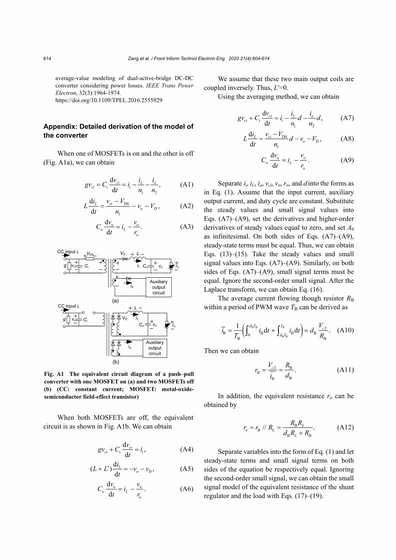
When one of MOSFETs is on and the other is off (Fig. A1a), we can obtain
i
i i i1 2
d,
dc αL
cv iigv C it n n
= = − − (A1)
i DSo D
1
d,
d−
= − −cL v ViL v V
t n (A2)
o oo
o
d.
d= −L
v vC it r
(A3)
When both MOSFETs are off, the equivalent circuit is as shown in Fig. A1b. We can obtain
i
i i id
,d
cc
vgv C it
+ = (A4)
o Dd( ) ,d
LiL L v vt
′+ = − − (A5)
o oo
o
d.
d Lv v
C it r= − (A6)
We assume that these two main output coils are coupled inversely. Thus, L′=0.
Using the averaging method, we can obtain
ii i i
1 2
d,
dc αL
cv iigv C i d dt n n
+ = − − (A7)
i DSo D
1
d ,d
cL v ViL d v Vt n
−= − − (A8)
o oo
o
d.
d Lv v
C it r= − (A9)
Separate ii, iL, ia, vci, vo, ro, and d into the forms as
in Eq. (1). Assume that the input current, auxiliary output current, and duty cycle are constant. Substitute the steady values and small signal values into Eqs. (A7)–(A9), set the derivatives and higher-order derivatives of steady values equal to zero, and set A0 as infinitesimal. On both sides of Eqs. (A7)–(A9), steady-state terms must be equal. Thus, we can obtain Eqs. (13)–(15). Take the steady values and small signal values into Eqs. (A7)–(A9). Similarly, on both sides of Eqs. (A7)–(A9), small signal terms must be equal. Ignore the second-order small signal. After the Laplace transform, we can obtain Eq. (16).
The average current flowing though resistor RB within a period of PWM wave TB can be derived as
( )B B B
B B
2B B B B0
B B
1 d d .= + =∫ ∫d T T c
d T
Vi i t i t d
T R (A10)
Then we can obtain
2 BB
BB
.cV Rr
di= = (A11)
In addition, the equivalent resistance ro can be
obtained by
Bo B L
B B
// .L
L
R Rr r Rd R R
= =+
(A12)
Separate variables into the form of Eq. (1) and let
steady-state terms and small signal terms on both sides of the equation be respectively equal. Ignoring the second-order small signal, we can obtain the small signal model of the equivalent resistance of the shunt regulator and the load with Eqs. (17)–(19).
Auxiliaryoutputcircuit
Auxiliaryoutputcircuit
Civcig
CC input ii VDS VD L
iL Co vo ro
ia
ia
CC input ii
Civcig VD iLCo vo
L
ro
(a)
(b)
Fig. A1 The equivalent circuit diagram of a push–pull converter with one MOSFET on (a) and two MOSFETs off (b) (CC: constant current; MOSFET: metal-oxide- semiconductor field-effect transistor)


![Practical methodology for analyzing the effect of conductor … · 2012-11-05 · Practical methodology for analyzing the effect of conductor roughness on signal ... [19] to affect](https://img.pdfslide.us/doc/110x75/5ec9630e8f6a78529a1d94c9/practical-methodology-for-analyzing-the-effect-of-conductor-2012-11-05-practical.jpg)