Embed Size (px)
Citation preview

2017
UNIVERSIDADE DE LISBOA
FACULDADE DE CIÊNCIAS
DEPARTAMENTO DE FÍSICA
A multiplexed organ-on-chip device for the study of the Blood-
Brain Barrier
Marciano Palma do Carmo
Mestrado Integrado em Engenharia Biomédica e Biofísica
Perfil em Radiações em Diagnóstico e Terapia
Dissertação orientada por:
Marinke van der Helm, MSc. e Dr. Hugo Ferreira

2017
UNIVERSITY OF LISBON
FACULTY OF SCIENCES
DEPARTMENT OF PHYSICS
A multiplexed organ-on-chip device for the study of the Blood-
Brain Barrier
Marciano Palma do Carmo
Integrated Master in Biomedical Engineering and Biophysics
Profile in Radiations in Diagnosis and Therapy
Dissertation guided by Marinke van der Helm, MSc. and Dr. Hugo Ferreira, and co-supervised
by Dr. Loes Segerink


“The important thing is not to stop questioning.”
Albert Einstein

vii
Acknowledgments
My deepest and sincere gratitude is to my daily supervisor, Marinke van der Helm, not only for her
excellent supervision and for teaching me everything, but also for all her help, patience, and especially
friendship. You did your best to make me feel at home and you definitely succeeded with it, so thank
you very much! Furthermore, I thank Loes Segerink for her keen eye on science and all her enthusiasm
for the project, from which I benefited a lot, and also for never saying no every time I came into her
office with a new crazy idea. I also want to thank Albert van der Berg for giving me the opportunity to
perform my Master’s assignment in such an amazing group. In addition, I want to thank Andries van
der Meer for all his guidance, expertise in organs-on-chips and for all the valuable ideas, discussions
and recommendations he gave me during the course of my work. Moreover, I want to thank my internal
supervisor, Hugo Ferreira, for all his supervision throughout this project and for his enthusiasm and
passion about biomedical engineering, in particular for micro and nanotechnologies, which contributed
greatly for my desire in doing my Master’s assignment in such a field.
Next, I want to thank the entire BIOS staff for all the provided help. In particular, I thank Johan
Bomer for teaching me everything I know about microfabrication, for letting me follow him inside the
cleanroom for days, and also for always being willing to try any idea I came up with, even though he
knew from the start that most of them would fail terribly. I also want to thank Paul ter Braak for the
course on cell culturing, all his help with cell-related issues, and for making the BioLab such a fun place
to be. Furthermore, I want to thank Hans de Boer for fabricating both my chip holder and the mold I
used for PDMS membrane fabrication. I also want to thank Anne Leferink for inviting me to be her
teaching assistant, from which I learned a lot on membrane fabrication, and for giving and letting me
use several of her materials. Next, I want to thank Hai Le The for all his help with my abstract
submission, cleanroom-related issues, for all his enthusiasm in membrane fabrication, and for being
such a nice guy to be with. You are the person who made the cleanroom and the cycling back home fun!
Furthermore, I want to thank Hugo Albers for teaching me everything he knew on PDMS chip
fabrication, for his help with CleWin and COMSOL, for being such a nice roommate in the student
corner, and for all the fun times we had around Enschede! I also want to thank Josh Loessberg-Zahl for
all the fruitful discussions and fun times in the lab. In addition, I thank Mathijs Bronkhorst, my other
student corner roomie, for all his help with COMSOL and for teaching and letting me use his setup. I
also owe thanks to Martijn Tibbe for letting me use his setup, Wesley van den Beld for growing the
nitride layer for my membranes and Andrea Minuto for all the help with fabricating my devices in the
DesignLab. Furthermore, I want to thank all the BIOS members for being such an amazing group of
people who made me feel at home for ten months and helped me out whenever I needed. The group
activities were a lot of fun, in particular the barbecue, the mountain biking, and the weekly football
games.

viii
Last, but not least, I am thankful for all the support my parents, family and friends gave me not
only during these ten months but since I started the journey of becoming a biomedical engineer. In
particular, I thank my girlfriend Margarida for all her support, for putting up with me and not turning
off our skype chats every time I started talking about work, and especially for her uplifting personality.
Your love has made all the difference.
ix
Abstract
The blood-brain barrier (BBB) constitutes a complex interface between blood and the central
nervous system (CNS), playing a vital role in maintaining brain homeostasis and protecting it from most
toxic substances and pathogens. However, due to the extremely low permeability that arises from the
tight junctions formed by the endothelial cells, the BBB also inhibits the brain uptake of many
pharmaceuticals, therefore posing a major obstacle for drug development studies. Furthermore, the
disturbance of the function of this unique structure can lead to many neurodegenerative disorders that
are not yet fully understood, such as brain tumors or Alzheimer’s disease.
There have been several attempts to establish reliable in vivo and in vitro models of the BBB that
can increase the knowledge on such pathological states of the brain and provide useful insights on drug
delivery across this barrier. However, as in vivo models require expensive and specific equipment, are
labor intensive, and give rise to many ethical and moral concerns, much effort is being put into
developing an in vitro model that truthfully resembles the BBB and is easy to analyze, reproducible, and
allows higher throughput screening than the in vivo models. Therefore, the main goal of the present
work was to design, fabricate and validate a microfluidic chip that could serve as a tool for the study of
the blood-brain barrier and allowed the creation of several different experimental conditions at the same
time in the same chip, thus increasing the throughput of the system. Two different models, a two-
dimensional and a three-dimensional, were fabricated for this purpose.
The first model that was built, which consisted of two poly(dimethylsiloxane) (PDMS) parts with
a membrane in between, allowed the monitoring of the tightness of the endothelial cell layers by
integrating on-chip transendothelial electrical resistance (TEER) and permeability analysis. Even though
preliminary, the results obtained for both these assays were quite encouraging and TEER and
permeability were found to be as high as 27.5 Ω·cm2 and as low as 3.6·10-5 cm/s, respectively. Moreover,
polystyrene (PS), silicon-rich nitride (SiRN) and PDMS membranes were fabricated in order to improve
the permeable supports on which cells were seeded inside this device. The second model, on the other
hand, was made in plexiglas and allowed the creation of lumen-shaped three-dimensional structures
within collagen on which cells were seeded. No experiments regarding TEER or permeability were
performed in the second model, although permeability studies could be done with the appropriate
protocol.
The capability of individually addressing the microfluidic chambers without any mixing occurring
between them was proven for both devices in experiments using dyes, trypsin and ethanol. Furthermore,
confluent monolayers of endothelial cells were observed in the two models with both phase contrast and
fluorescence microscopy, making it possible for us to conclude that two different yet equally
physiologically relevant multiplexed devices that allow the individual addressing of their microfluidic
chambers had been developed.
However, further experimenting is required in order to fully characterize the devices, especially
concerning TEER measurements, permeability assays and dynamic cell culturing. Moreover, finding a
coating agent that would allow the use of lower concentrations of collagen to fabricate the hollow
channels would make the second model more advantageous. Furthermore, the co-culture of endothelial
cells with other cell types that are known to enhance the tightness of the BBB, such as astrocytes or

x
pericytes, should also be looked into for both devices. Performing on-chip drug screening studies would
also be of interest.
Keywords: BBB-on-chip, blood-brain barrier, microfluidics, microfabrication, organs-on-chips.
xi
Sumário em Português
A barreira hemato-encefálica representa a mais complexa interface entre o sangue e o sistema
nervoso central, sendo bastante importante na manutenção da homeostasia do cérebro e em proteger o
mesmo de diversas substâncias tóxicas e patogénicas. Contudo, devido à baixa permeabilidade que
advém das ligações formadas entre as diversas células endoteliais, esta barreira inibe também a entrada
de vários agentes farmacêuticos no cérebro, constituindo assim um grande obstáculo ao
desenvolvimento de novas terapias. Para além disto, qualquer pertubação no funcionamento desta
estrutura pode originar diversas doenças neurodegenerativas.
Várias têm sido as tentativas de desenvolver um modelo fidedigno da barreira hemato-encefálica,
quer in vivo, ex-vivo, in silico e in vitro, que ajude a melhor compreender estes estados patológicos do
cérebro e que possa fornecer novas perspectivas acerca do transporte de agentes terapêuticos através
desta barreira. No que diz respeito aos modelos in vivo, estes não só requerem equipamento bastante
específico e caro, como também são bastante morosos e dão origem a diversas questões éticas e morais.
Os modelos ex-vivo, por outro lado, permitem analisar tecidos vivos, os quais podem ser fatias de um
órgão ou o órgão completo, fora do seu contexto biológico, permitindo desta forma um maior controlo
de todas as condições experimentais do que os modelos in vivo. No entanto, garantir que o ambiente
artificial em que o tecido é analisado tenha exactamente as mesmas condições que o seu ambiente
biológico pode tornar-se complicado, o que pode por sua vez causar a morte do tecido. No caso dos
modelos in silico, estes são construídos com recurso a modelos computacionais baseados em dados
obtidos em experiências realizadas in vivo, o que os torna bastante fidedignos em prever, por exemplo,
a permeabilidade da barreira hemato-encefálica a um determinado medicamento. O facto destes modelos
muitas vezes não terem em conta toda a complexidade da barreira hemato-encefálica é uma das suas
limitações. No caso dos modelos in vitro, estes permitem o estudo das mais variadas estruturas
biológicas fora do seu contexto natural. Para tal, células derivadas de tecidos cerebrais são cultivadas
em modelos construídos propositadamente para o estudo em questão, o que permite um maior controlo
sobre todas as condições experimentais. Deste modo, é perceptível que muitos esforços têm sido feitos
para desenvolver um modelo in vitro que simule correctamente a barreira hemato-encefálica e que seja
de fácil análise, reprodutível, e permita um maior rastreio (de agentes terapêuticos, por exemplo) que os
modelos in vivo.
O objectivo principal deste trabalho foi desenvolver e validar um chip microfluídico que pudesse
ser usado como uma ferramenta para o estudo da barreira hemato-encefálica e que permitisse a criação
de diferentes condições experimentais ao mesmo tempo, no mesmo chip. Para atingir este objectivo,
foram construídos dois modelos diferentes: um bi-dimenisonal e um tri-dimensional.
O primeiro modelo construído, o qual consistia em duas partes de dimetil polissiloxano com uma
membrana entre elas, foi replicado a partir de um molde feito de silício, o qual por sua vez foi fabricado
numa sala estéril com recurso a técnicas de microfabricação. Células endoteliais foram cultivadas neste
modelo e as barreiras formadas pelas mesmas mantiveram-se viáveis, em todos os casos, durante pelo
menos cinco dias de cultura celular, período após o qual o núcleo e o citoesqueleto das células foram
coloridos de modo a verificar a integridade das barreiras formadas. Este modelo possibilitou ainda a

xii
monitorização da complexidade das barreiras de células endoteliais ao integrar funcionalidades que
permitiam a análise da resistência eléctrica transendotelial e da permeabilidade das mesmas. Embora
preliminares, os resultados obtidos em ambos os testes foram bastante encorajadores e os valores obtidos
para a resistência eléctrica e para a permeabilidade das barreiras foram de 27.5 Ω·cm2 e 3.6·10-5 cm/s,
respectivamente. Para além disto, foram também fabricadas membranas feitas de poliestireno, nitrato
rico em silício e dimetil polissiloxano, com o intuito de substituir os suportes permeáveis feitos em
policarbonato nos quais as células eram cultivadas.
O segundo modelo, por outro lado, foi feito em acrílico. Para tal, um bloco de acrílico foi cortado
a laser e as diferentes peças foram coladas umas às outras com recurso a um adesivo biocompatível.
Depois de montado o chip, um gel de colagénio foi inserido em cada um dos compartimentos do mesmo
e micro-agulhas foram posicionadas por entre os buracos das tampas do chip. Depois de solidificar o
colagénio, as micro-agulhas foram cuidadosamente retiradas. Isto permitiu a criação, em colagénio, de
estruturas tridimensionais em forma de lúmen nas quais as células foram cultivadas. Tal como no modelo
bi-dimensional, as células endoteliais cultivadas no colagénio mantiveram-se viáveis durante pelo
menos cinco dias de cultura celular. Não foram realizadas neste modelo quaisquer experiências que
tivessem como intuito determinar a resistência eléctrica e a permeabilidade das barreiras de células
endoteliais, embora estudos de permeabilidade pudessem ser feitos com o protocolo adequado.
A capacidade de utilizar individualmente os diferentes compartimentos microfluídicos sem que
ocorresse qualquer mistura entre os mesmos foi provada em ambas as plataformas. Em relação ao
modelo bi-dimenional, foram realizadas, numa primeira fase, experiências com corantes, enquanto numa
segunda fase tripsina, álcool e meio de cultura foram inseridos nos diferentes compartimentos
microfluídicos para confirmar se ocorria alguma mistura das soluções que afectasse as diversas barreiras
celulares. Para tal, os chips foram ligados a uma bomba microfluídica que puxou as diversas soluções
em todos os compartimentos microfluídicos. No caso das experiências em que foram utilizados
trisipsina, álcool e meio de cultura, foi realizada uma coloração para verificar a viabilidade das barreiras
celulares no final da experiência, a qual revelou que os diferentes compartimentos podiam ser utilizados
sem que houvesse qualquer contaminação entre os diferentes compartimentos que pudesse pôr em causa
a integridade das barreiras celulares. No que diz respeito ao modelo tri-dimensional, a capacidade de
utilizar individualmente os diversos compartimentos foi apenas provada ao introduzir os diferentes
corantes nos mesmos, o que revelou que o método de fabricação do chip assegurava uma plataforma
robusta na qual diversas experiências podiam ser realizadas sem qualquer risco de contaminação. Para
além disto, foi também possível cultivar células endoteliais neste chip durante pelo menos cinco dias,
embora a coloração das mesmas não tenha sido bem sucedida uma vez que os agentes fluorescentes se
difundiram pelo colagénio. Isto fez com que fosse possível concluir que, embora diferentes, dois
modelos igualmente relevantes em termos fisiológicos tinham sido desenvolvidos.
Contudo, ambos os modelos necessitam de uma caracterização mais profunda. No caso do primeiro
modelo, este beneficiaria caso melhorias fossem feitas no que diz respeito a medições de resistência
eléctrica, de permeabilidade, e também de cultura dinâmica de células. Para tal, experiências futuras e
protocolos adequados são necessários. No caso do segundo modelo, encontrar um agente que permita
revestir as estruturas em acrílico de modo a que seja possível utilizar concentrações mais baixas de
colagénio seria bastante benéfico. Para além disto, a criação de co-culturas de células endoteliais com
células cerebrais que são conhecidas por aumentar a complexidade e a impermeabilidade da barreira
hemato-encefálica, tais como astrócitos ou perócitos, devia também ser realizada em ambos os modelos
de modo a verificar se as mesmas aumentariam a complexidade da barreira hemato-encefálica formada,
como descrito na literatura. Por último, seria também de elevado interesse realizar testes de rastreio de
diversos agentes farmacêuticos utilizados no tratamento de várias patologias, como por exemplo para as
doenças de Alzheimer e de Parkinson, de modo a obter novas perspecivas no que à permeabilidade da
barreira hemato-encefálica a estas substâncias diz respeito.
Palavras-chave: BHE-em-chip, barreira hemato-encefálica, microfluídica, microfabricação,
órgãos-em-chips.
xiii
Contents
Acknowledgments ................................................................................................................................ vii
Abstract ................................................................................................................................................. ix
Sumário em Português ......................................................................................................................... xi
List of figures ..................................................................................................................................... xvii
List of tables ........................................................................................................................................ xxi
List of abbreviations ......................................................................................................................... xxiii
1 Introduction ........................................................................................................................................ 1
1.1 Project description ........................................................................................................................1
1.2 Preview ........................................................................................................................................1
2 Background & theory ........................................................................................................................ 3
2.1 Anatomy and physiology of the blood-brain barrier ....................................................................3
2.2 Ways to study the BBB ................................................................................................................5
2.3 In vitro BBB model evaluation.....................................................................................................7
2.3.1 Cells ...................................................................................................................................... 8
2.3.2 Shear stress ........................................................................................................................... 8
2.3.3 Permeability .......................................................................................................................... 9
2.3.4 Transendothelial electrical resistance ................................................................................. 10
2.4 Existing microfluidic BBB models ............................................................................................ 14
2.5 Summary .................................................................................................................................... 17
3 Microfluidic devices design .............................................................................................................. 19
3.1 Single BBB chip ......................................................................................................................... 19
3.1.1 Design and fabrication ........................................................................................................ 19
3.1.2 Drawbacks & requirements ................................................................................................ 20
3.2 2D Multiplexed BBB chip .......................................................................................................... 20
3.2.1 Chip and photomask design ............................................................................................... 20
3.2.2 Mold fabrication ................................................................................................................. 22
3.3 3D BBB Device .......................................................................................................................... 23
3.3.1 Design and Fabrication ....................................................................................................... 23
4 Membrane fabrication ..................................................................................................................... 25
xiv
4.1 Methods ...................................................................................................................................... 25
4.1.1 Polystyrene membrane ....................................................................................................... 25
4.1.2 Silicon-rich nitride membrane ............................................................................................ 25
4.1.3 Polydimethylsiloxane membrane ....................................................................................... 27
4.2 Results & discussion .................................................................................................................. 30
4.2.1 Polystyrene membrane ....................................................................................................... 30
4.2.2 Silicon-rich nitride membrane ............................................................................................ 31
4.2.3 Polydimethylsiloxane membrane ....................................................................................... 32
5 Microfluidic devices validation ....................................................................................................... 35
5.1 Methods ...................................................................................................................................... 35
5.1.1 Device fabrication .............................................................................................................. 35
5.1.2 Fluidic characterization of two-dimensional devices ......................................................... 37
5.1.3 Characterization of lumen robustness in the 3D devices .................................................... 39
5.1.4 On-chip cell culture ............................................................................................................ 39
5.1.5 Cell observation .................................................................................................................. 41
5.1.6 Mechanical modulation ...................................................................................................... 41
5.1.7 Individually addressable channels ...................................................................................... 42
5.1.8 Dextran permeability assay ................................................................................................ 43
5.1.9 TEER assay ........................................................................................................................ 44
5.2 Results ........................................................................................................................................ 46
5.2.1 Device fabrication .............................................................................................................. 46
5.2.2 Fluidic characterization ...................................................................................................... 51
5.2.3 Characterization of lumen robustness in the 3D devices .................................................... 54
5.2.4 On-chip cell culture ............................................................................................................ 55
5.2.5 Mechanical modulation ...................................................................................................... 60
5.2.6 Individually addressable channels ...................................................................................... 60
5.2.7 Dextran permeability analysis ............................................................................................ 64
5.2.8 TEER analysis .................................................................................................................... 66
6 Conclusion ......................................................................................................................................... 69
7 Recommendations & future perspectives ....................................................................................... 71
8 Bibliography ..................................................................................................................................... 73
Appendices ........................................................................................................................................... 79
A Conference submission .................................................................................................................... 81
xv
B MATLAB scripts ............................................................................................................................. 85
B.1 MATLAB script for the calculation of flow profile .................................................................... 85
B.2 MATLAB script for tracking particles ........................................................................................ 87
B.3 MATLAB script for computing the positions of the tracked particles ........................................ 95
B.4 MATLAB script for calculating the velocities of the tracked particles from the saved tracks .... 96
C Supplementary information ........................................................................................................... 99
C.1 Fluidic characterization ............................................................................................................. 99
C.2 Mechanical modulation ........................................................................................................... 100
C.3 Channels individually addressed using trypsin and EGM-2 .................................................... 100
C.4 Dextran permeability assay ...................................................................................................... 101
C.5 TEER assay .............................................................................................................................. 101
C.6 3D device ................................................................................................................................. 103
D Additional Images .......................................................................................................................... 105

xvi
xvii
List of figures
Figure 2.1 – Schematic representation of the BBB ................................................................................ 3
Figure 2.2 – Structure of BBB tight and adherens junctions .................................................................. 4
Figure 2.3 – Main routes of molecular transport across the BBB .......................................................... 5
Figure 2.4 – Equivalent circuit diagram describing the contribution of the trans- and paracellular
pathway to the total impedance, Z, of the cellular system .................................................................... 12
Figure 2.5 – Impedance simulation of a cell monolayer on a chip ....................................................... 13
Figure 2.6 - Models of the BBB reported in literature ......................................................................... 14
Figure 3.1 - Design of the current BBB chip ........................................................................................ 19
Figure 3.2 – Fully assembled (A) and exploded view (B) of the 2D BBB multiplex device ............... 21
Figure 3.3 – Photomasks design ........................................................................................................... 21
Figure 3.4 – Fabrication process of the molds ...................................................................................... 22
Figure 3.5 – Fully assembled (A) and exploded view (B) of the 3D BBB multiplex device ............... 23
Figure 4.1 - Schematic representation of the SiRN membrane fabrication process ............................. 26
Figure 4.2 - Schematic representation of the Si stamp fabrication process .......................................... 27
Figure 4.3 – Fabrication process of porous PDMS membranes with the aid of a Si stamp ................. 28
Figure 4.4 - Fabrication process of PDMS membranes ........................................................................ 29
Figure 4.5 - Fabricated PS membrane .................................................................................................. 30
Figure 4.6 - Fabricated porous SiRN membrane .................................................................................. 31
Figure 4.7 – SEM image of the pillars in the fabricated Si stamp ........................................................ 32
Figure 4.8 – Broken Si pillars on the stamp (left) and on the PS sheet (right) ..................................... 32
Figure 4.9 – Continuous PDMS membrane .......................................................................................... 33
Figure 4.10 – Porous PDMS membrane ............................................................................................... 34
Figure 4.11 - (Semi-)Porous PDMS membrane, fabricated by curing the first layer of resist at 120ºC for
10 min, before (A) and after being peeled off the wafer (B and C) ...................................................... 34
Figure 5.1 – Schematic illustration of the two-layer PC membrane-based devices ............................. 36
Figure 5.2 - Schematic illustration of the two-layer PDMS membrane-based devices ........................ 37
Figure 5.3 – Dynamic culture setup. .................................................................................................... 42
Figure 5.4 - Schematic representation of the experiments with food dye, trypsin and ethanol in every
other outlet of the 2D BBB multiplex device ........................................................................................ 43
Figure 5.5 - Schematic representation of the on-chip dextran permeability assay ............................... 44
Figure 5.6 - Schematic illustration of the top view of the BBB multiplex device with Pt electrodes (A)
and of the electrical circuit of a cell layer on one of the channels of the BBB multiplex device (B) ... 45
Figure 5.7 – Fabrication of single-layer PDMS on glass devices ......................................................... 46
Figure 5.8 – Problems in the fabrication of two-layer PC membrane-based PDMS devices using the
toluene/PDMS mortar............................................................................................................................ 47
Figure 5.9 – A) Fully assembled two-layer device with a PC membrane and B) Highlight of a fully
enclosed channel after hCMEC/D3 cells were loaded into the device ................................................. 48
xviii
Figure 5.10 – A), B) Fabrication and C) schematic illustration, of two-layer PDMS membrane-based
devices ................................................................................................................................................... 48
Figure 5.11 – A), B) Single BBB device with a PDMS membrane and C) respective schematic
illustration .............................................................................................................................................. 49
Figure 5.12 – Fully assembled two-layer PDMS membrane-based device with Pt electrodes ............ 49
Figure 5.13 – 3D multiplex BBB device both fully assembled and separated in pieces ...................... 50
Figure 5.14 – Beads and fluorescein distribution throughout the channels of the 2D BBB multiplex
devices ................................................................................................................................................... 51
Figure 5.15 – Flow inside the 2D BBB multiplex device..................................................................... 52
Figure 5.16 – Flow rates inside the microfluidic devices obtained empirically ................................... 53
Figure 5.17 – Assessing the integrity of the three hollow lumens inside Collagen I ........................... 54
Figure 5.18 – Stained cells inside a single-layer PDMS on glass device: blue – nuclei; green – f-actin
............................................................................................................................................................... 55
Figure 5.19 – Cells inside two of the channels of a two-layer PC membrane-based device ................ 56
Figure 5.20 – hCMEC/D3 viability on the PC membrane: green (Calcein – AM) – live cells ............ 56
Figure 5.21 – Staining of hCMEC/D3 cell layer on the PC membrane: blue – nuclei, green – f-actin 57
Figure 5.22 – Cells inside two of the channels of a two-layer PDMS membrane-based device .......... 58
Figure 5.23 – Staining of the hCMEC/D3 cells on a two-layer device with a PDMS membrane. Blue –
nuclei, green – f-actin ............................................................................................................................ 59
Figure 5.24 – hCMEC/D3 cells seeded in one the A) top and B) bottom parts of one of the Collagen I
lumens fabricated inside the 3D BBB multiplex chip ........................................................................... 59
Figure 5.25 – hCMEC/D3 cells on one of the microfluidic channel before and after dynamic culture 60
Figure 5.26 – Individually addressable channels of the BBB multiplex device with blue, yellow, red
and green food dyes ............................................................................................................................... 61
Figure 5.27 – Food dyes inside the three-dimensional BBB multiplex chip ........................................ 61
Figure 5.28 – Trypsin experiment: Cells inside two channels of the BBB device before, during and after
(live/dead staining) 0.05% trypsin and normal EGM-2 culture medium were flushed in every other
channel .................................................................................................................................................. 62
Figure 5.29 – Live/dead staining of the cells inside the microfluidic device after normal EGM-2 and
5% ethanol were pulled from every other outlet. Blue – nuclei, green – calcein AM (live cells), red –
ethidium homodimer-1 (dead cells) ...................................................................................................... 63
Figure 5.30 – Live/dead staining of the hCMEC/D3 cells in the areas where the channels merge with
each other in the experiments with A) trypsin and B) ethanol. Blue – nuclei, green – calcein AM (live
cells), red – ethidium homodimer-1 (dead cells) ................................................................................... 64
Figure 5.31 – Permeability coefficients of the eight BBBs of device 1 to the 40 kDa dextran ............ 64
Figure 5.32 – Average TEER values obtained for the eight cell barriers inside the BBB multiplex device
at different time points after seeding the cells (at t = 0 h) ..................................................................... 66
Figure C.1 – Plot of the velocities inside the microfluidic channels of the BBB device obtained with
COMSOL .............................................................................................................................................. 99
Figure C.2 – Air trapped inside the microfluidic channels when investigating the influence of fluidic
shear stress in cell growth, morphology and proliferation .................................................................. 100
Figure C.3 – Permeability coefficients of the eight BBB’s of device 2 to the 40 kDa dextran.......... 100
Figure C.4 – Channels of the 2D BBB multiplex device individually addressed using trypsin and EGM-
2. Blue – nuclei; green – Calcein AM (live cells); red – Ethidium homodimer-1 (dead cells) ........... 101
Figure C.5 – Impedance spectra obtained in obtained for channel 1 of device 2 when A) there were no
cells in the device and when B) hCMEC/D3 cells had been seeded ................................................... 102
Figure C.6 – Nuclei (blue) and f-actin (green) staining of the hCMEC/D3 cells on collagen I inside the
3D BBB-on-chip device ...................................................................................................................... 103
Figure D.1 - Si mold with SU-8 structures for the fabrication of simple BBB multiplex devices ..... 105
Figure D.2 - Si mold with SU-8 structures for the fabrication of BBB multiplex devices with Pt
electrodes ............................................................................................................................................. 105

xix
Figure D.3 – Chip holder used in fabrication of 2D devices .............................................................. 106
Figure D.4 – Mold for the fabrication of the PDMS rings A) dismounted and B) fully assembled ... 106
Figure D.5 – Diced Si stamp (left) and SiRN membrane (right) ........................................................ 106

xx
xxi
List of tables
Table 5.1 – Measured average flow rates, and corresponding calculated shear rates, inside the
microfluidic channels ............................................................................................................................ 53
Table C.1 – TEER values obtained for the cell layers seeded in device 1 ....................................... 101
Table C.2 – TEER values obtained for the cell layers seeded in device 2 ....................................... 102
Table C.3 – TEER values obtained for the cell layers seeded in device 3 ....................................... 102

xxii
xxiii
List of abbreviations
AC Alternating current
ACM Astrocyte-conditioned medium
AJs Adherens junctions
BBB Blood-brain barrier
BL Basal lamina
BSA Bovine serum albumin
CCL Cell layer capacitance (F)
CDL Double-layer capacitance (F)
CEL Electrode capacitance (F)
Cmem Cell membrane capacitance (F)
CNS Central nervous system
DC Direct current
DI Deionized water
DMSO Dimethylsulfoxide
EAE Experimental allergic encephalomyelitis
EBM-2 Endothelial basal medium-2
EGM-2 Endothelial growth medium-2
EVOM Epithelial Voltohmmeter
FDTS Perfluorodecylthrichlorosilane
FN Fibronectin
fTEER Frequency at which TEER is read (Hz)
GBM Glioblastoma multiform
hBMVEC Human brain-derived microvascular endothelial cells
hCMEC/D3 Human cerebral microvascular endothelial cells
hiPSC Human induced pluripotent stem cells
HMDS Hexamethyldisilazane
HNO3 Nitric acid
ID Inner diameter
JAMs Junctional adhesion molecules
KOH Potassium hydroxide
LPCVD Low-pressure chemical vapor deposition
N2 Nitrogen
NaOH Sodium hydroxide
NVU Neurovascular unit
OD Outer diameter
OSP One side polished
xxiv
PB Permeabilization buffer
PBS Phosphate-buffered saline
PC Polycarbonate
PCTE Polycarbonate track-etched
PDMS Poly (dimethylsiloxane)
PE Polyester
PET Polyethylene terephthalate
PMMA Poly (methylmethacrylate)
PS Polystyrene
Pt Platinum
PT790 Plasma term 790
PTFE Polytetrafluoroethylene
PVP Polyvinylpyrrolidone
QDR Quick dump rinse
RIE Reactive ion etching
Rmed Medium resistance (Ω)
Rmembrane Membrane resistance (Ω)
Rpores Resistance of medium inside membrane pores (Ω)
RTEER TEER resistance (Ω)
RPM Rotations per minute
RT Room temperature
SCCM Standard cubic centimeter per minute
SEM Scanning electron microscope / microscopy
SF6 Sulfur hexafluoride
Si Silicon
SiRN Silicon rich nitride
TEER Transendothelial electrical resistance
TJs Tight junction
TNF-α Tumor necrosis factor alpha
UV Ultraviolet
Zmem Membrane impedance
ZO-1 Zonula Occludens 1

1
Chapter 1
Introduction
1.1 Project description
The final goal of the present work is to develop a multiplexed organ-on-chip platform for the study
of the blood-brain barrier (BBB) that allows the creation of different experimental conditions at the same
time (e.g., for the screening of different drugs), thus reducing the elapsed time between experiments and
enhancing the throughput of the system. In order to do this, the current microfluidic model of the BBB
used at BIOS Lab on a Chip group was redesigned, with the main goal of fabricating a new device that
could allow several parallel and compartmentalized cultures of brain endothelial cells. Moreover,
improvements were also made to the supports on which cells are grown. After thorough characterization,
the validity of the multiplex organ-on-chip device as a reliable model of the BBB was investigated.
1.2 Preview
In the next chapter the anatomy and physiology of the BBB, as well as the standard ways to mimic
it, will be described. Furthermore, the most common ways to evaluate the functionality of a BBB model
will also be explained. Subsequently, the procedures that were used to design the microfluidic devices
and the molds from which these were replicated are detailed. In chapter 4, the methods and
corresponding results for the fabrication of different types of membranes to integrate in the BBB device
are described. The methods and results regarding device validation, specifically the fabrication of the
different devices, the on-chip culturing of cells, and the different experiments performed on the devices
are displayed and discussed in chapter 5. After this, conclusions and future prospects about this work
are depicted.
Finally, in appendix A the paper ‘Individually addressable channels in a multiplexed organ-on-
chip device’, and the corresponding poster, that was accepted at the MicroNano Conference (13-14
December 2016, Amsterdam, the Netherlands) is included and in appendices B, C and D the MATLAB
scripts, supplementary information concerning some of the experiments and figures of important parts
and tools that were used throughout this project are shown, respectively.

2
3
Chapter 2
Background & theory
2.1 Anatomy and physiology of the blood-brain barrier
The Blood-Brain Barrier (BBB) is a highly selective structure in the central nervous system that
separates the circulating blood from the extracellular brain fluids. This structure is formed by endothelial
cells, which constitute the walls of the brain capillaries with a combined surface area that makes it the
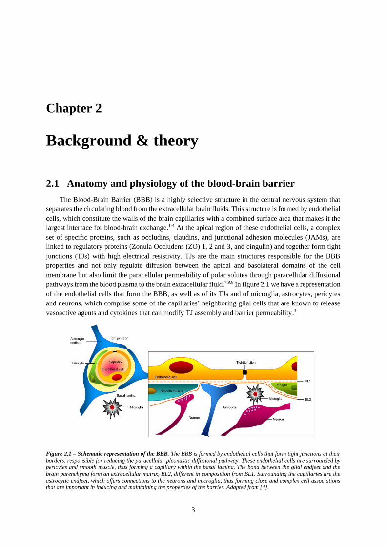
largest interface for blood-brain exchange.1-4 At the apical region of these endothelial cells, a complex
set of specific proteins, such as occludins, claudins, and junctional adhesion molecules (JAMs), are
linked to regulatory proteins (Zonula Occludens (ZO) 1, 2 and 3, and cingulin) and together form tight
junctions (TJs) with high electrical resistivity. TJs are the main structures responsible for the BBB
properties and not only regulate diffusion between the apical and basolateral domains of the cell
membrane but also limit the paracellular permeability of polar solutes through paracellular diffusional
pathways from the blood plasma to the brain extracellular fluid.7,8,9 In figure 2.1 we have a representation
of the endothelial cells that form the BBB, as well as of its TJs and of microglia, astrocytes, pericytes
and neurons, which comprise some of the capillaries’ neighboring glial cells that are known to release
vasoactive agents and cytokines that can modify TJ assembly and barrier permeability.3
Figure 2.1 – Schematic representation of the BBB. The BBB is formed by endothelial cells that form tight junctions at their
borders, responsible for reducing the paracellular pleonastic diffusional pathway. These endothelial cells are surrounded by
pericytes and smooth muscle, thus forming a capillary within the basal lamina. The bond between the glial endfeet and the
brain parenchyma form an extracellular matrix, BL2, different in composition from BL1. Surrounding the capillaries are the
astrocytic endfeet, which offers connections to the neurons and microglia, thus forming close and complex cell associations
that are important in inducing and maintaining the properties of the barrier. Adapted from [4].
4
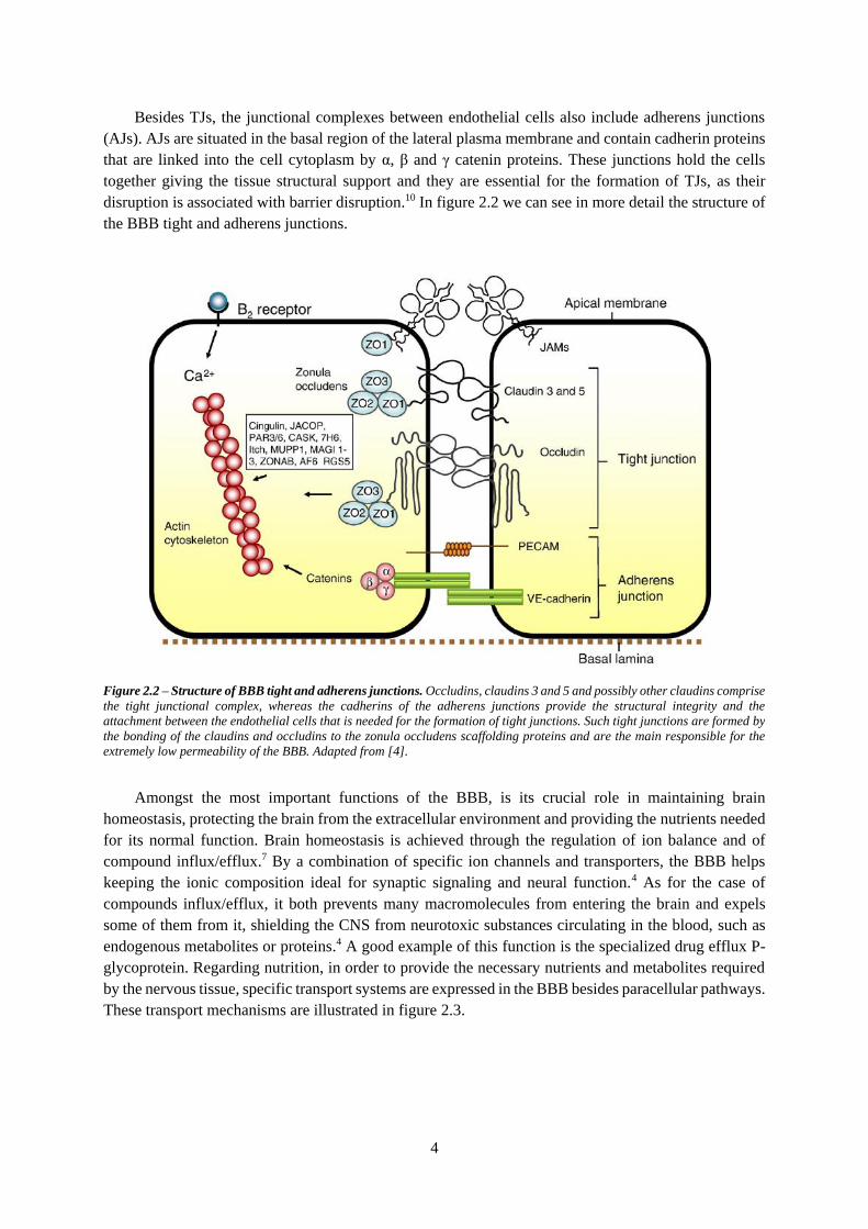
Besides TJs, the junctional complexes between endothelial cells also include adherens junctions
(AJs). AJs are situated in the basal region of the lateral plasma membrane and contain cadherin proteins
that are linked into the cell cytoplasm by α, β and γ catenin proteins. These junctions hold the cells
together giving the tissue structural support and they are essential for the formation of TJs, as their
disruption is associated with barrier disruption.10 In figure 2.2 we can see in more detail the structure of
the BBB tight and adherens junctions.
Amongst the most important functions of the BBB, is its crucial role in maintaining brain
homeostasis, protecting the brain from the extracellular environment and providing the nutrients needed
for its normal function. Brain homeostasis is achieved through the regulation of ion balance and of
compound influx/efflux.7 By a combination of specific ion channels and transporters, the BBB helps
keeping the ionic composition ideal for synaptic signaling and neural function.4 As for the case of
compounds influx/efflux, it both prevents many macromolecules from entering the brain and expels
some of them from it, shielding the CNS from neurotoxic substances circulating in the blood, such as
endogenous metabolites or proteins.4 A good example of this function is the specialized drug efflux P-
glycoprotein. Regarding nutrition, in order to provide the necessary nutrients and metabolites required
by the nervous tissue, specific transport systems are expressed in the BBB besides paracellular pathways.
These transport mechanisms are illustrated in figure 2.3.
Figure 2.2 – Structure of BBB tight and adherens junctions. Occludins, claudins 3 and 5 and possibly other claudins comprise
the tight junctional complex, whereas the cadherins of the adherens junctions provide the structural integrity and the
attachment between the endothelial cells that is needed for the formation of tight junctions. Such tight junctions are formed by
the bonding of the claudins and occludins to the zonula occludens scaffolding proteins and are the main responsible for the
extremely low permeability of the BBB. Adapted from [4].
5
Due to its highly selective permeability, the BBB only allows molecules smaller than,
approximately, 500 Da to easily cross it, which means that it not only protects the human brain from a
great amount of toxic substances but also inhibits several drug candidates from entering brain tissues
from capillaries, therefore posing a great hurdle to drug delivery to the brain. Moreover, loss of barrier
function is highly associated with several neurological disorders, such as brain tumors, multiple
sclerosis, Alzheimer’s and Parkinson’s diseases, brain edema, and many more. For example, the loss of
BBB integrity and barrier functionality caused by the impairment of the tight junctions of claudin-3, but
not claudin-5 or occludin, has been reported to be associated with conditions such as experimental
allergic encephalomyelitis (EAE) and glioblastoma multiform (GBM).4,12 Therefore, the need for more
intensive pre-clinical studies is clear, not only to develop new drug treatments and better understand
their passage across the BBB, but also to study the role of barrier function on CNS disease progression
and test innovative methods of delivery,15 as directing therapies to protect or repair the endothelium may
provide an effective way to reduce severity of neurological symptoms or delay onset of
neurodegeneration for many pathologies.2
2.2 Ways to study the BBB
Since the importance of the BBB has been understood, its physiology and pathology have been
widely studied through in vivo, ex vivo, in silico and in vitro studies, although in vivo and in vitro are
the mainly adopted approaches.
In vivo studies present the most relevant and direct method to study BBB physiology. With these
type of experimentations, in the case of the BBB, valuable information regarding the entire
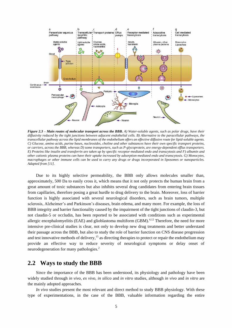
Figure 2.3 – Main routes of molecular transport across the BBB. A) Water-soluble agents, such as polar drugs, have their
diffusivity reduced by the tight junctions between adjacent endothelial cells. B) Alternative to the paracellular pathways, the
transcellular pathway across the lipid membranes of the endothelium offers an effective diffusive route for lipid-soluble agents.
C) Glucose, amino acids, purine bases, nucleosides, choline and other substances have their own specific transport proteins,
or carriers, across the BBB, whereas D) some transporters, such as P-glycoprotein, are energy-dependent efflux transporters.
E) Proteins like insulin and transferrin are taken up by specific receptor-mediated endo and transcytosis and F) albumin and
other cationic plasma proteins can have their uptake increased by adsorption-mediated endo and transcytosis. G) Monocytes,
macrophages or other immune cells can be used to carry any drugs or drugs incorporated in liposomes or nanoparticles.
Adapted from [11].
6
microenvironment of the brain and biological processes in live animals can be obtained, which can be
extremely advantageous when testing and validating other models.7 However, due to the differences
between humans and animals, most of these models fail to replicate the human response accurately16, 17
and therefore much attention has to be given when translating the obtained results from animal models
to humans. Furthermore, we also have to take into account not only the fact that these tests may be
highly costly and labour intensive,17 especially due to the costs for buying the animals and keeping them
alive, but also all the ethical and moral questions addressed to them.
Ex vivo studies are a type of experiments where a living tissue, which can be a whole organ, a
portion of it, or even a larger organ system, is analyzed outside of the organism in an artificial setup
with as little change as possible to in vivo conditions, therefore allowing more controlled conditions
when compared to in vivo experiments. Moreover, these experiments may also be performed on tissues
collected at autopsies and they avoid all the ethical and moral questions of performing experiments in
living subjects, which makes them a viable alternative to in vivo studies. In the case of the brain, one of
the most common ex vivo methods for its study are slices, where interactions between all the components
of the neurovascular unit (NVU) are preserved in a fashion close to the in vivo situation.7
In silico studies are carried out via computer simulations. In these methods, computational models
of the BBB are constructed based on in vivo experimental data, allowing for robust predictions, with
little need to recur to animals.18,19 Despite the fact that these models can be very useful in predicting, for
example, brain permeability to drugs or the properties of the different transport mechanisms across the
BBB, they still present some limitations as they do not fully take into account the complex nature of the
BBB.
In vitro techniques refer to models that allow the study of cells, or other biological features, outside
their normal biological context. As these models are fast, high-throughput, simple, can be thoroughly
analyzed and can be set up with healthy, modified or diseased human tissue20 and they can overcome
significant disadvantages posed by the models mentioned above, the pursuit for a reliable in vitro model
of the BBB has greatly increased. The ideal in vitro model should not only be simple and reproducible,
but it should also mimic as closely as possible the in vivo barrier both functionally and anatomically in
order to allow the study of BBB-related issues and drug delivery to the CNS.7 Essentially, in vitro BBB
models consist of primary cell cultures and cell lines of brain endothelial cells used to assess a wide
range of cell features and disease mechanisms. Not only can these models be designed for a specific
research question, granting the researcher control over a variety of parameters, as they often provide
cells with a controlled environment, making them relatively robust, reproducible, easy to analyze and
more fit for high-throughput screening than animal studies.20 Good examples of such in vitro models are
the Petri dish and the Transwell culture systems. Petri dish cultures form the most simple culture
systems, where cells are seeded on a dish with culture medium, and although they are too simple to carry
out some studies they are helpful when evaluating, e.g., the cytotoxicity of a certain drug. On the other
hand, the Transwell systems are the standard models for culturing barrier forming tissues and consist of
an improved culture setup with a suspended filter membrane normally made of polycarbonate or
polyester. This membrane divides the culture chamber in an apical and basolateral region and allows
more complex and functional studies, such as permeability and transendothelial electrical resistance
(TEER) measurements, and also the possibility to co-culture different types of cells on both sides of the
membrane, thus increasing the relevance of the model. The large surface area of these systems, however,
presents a considerable disadvantage as the difficulty in growing a uniform and confluent cell layer
increases and a single rupture can lead to erroneous results in permeability and TEER assays.
Furthermore, Transwell inserts only allow static culture conditions, therefore lacking the ability to
mechanically modulate the cell layer and assess the influence of fluidic shear stress exposure on cell
differentiation and migration. Such drawbacks may also influence permeability studies, as the analytes
cannot be introduced in the system at a constant rate and that may influence the transport of the
7
molecules across the membrane.23 To address these shortcomings, attempts have been made to
microengineer and integrate more realistic key aspects of the cell’s natural environment in these models.
One of these attempts are the organs-on-chips platforms.
Organs-on-chips are a class of three-dimensional microdevices, based on the principles of
microchip technology, designed to incorporate human living cell cultures that are grown in dynamic
engineered microenvironments derived from the organ. These engineered cell structures mimic the
minimal functional units of human healthy and diseased organs and tissues and allow biological,
chemical or physical manipulation, and analysis, through microfluidics, mechanical and electrical
stimulation, microelectronics, imaging and other high-tech methods, thus granting a high level of
spatiotemporal control over the culture conditions.20
Microfluidics is the science and technology that uses systems with channels with dimensions in the
order of tens to hundreds of micrometers to process small volumes of fluids.24 The main fields of
application of this technology are engineering, physics, chemistry, biology and nanotechnology and
among some of its advantages are its reduced costs and the fact that it offers the possibility to perform
analysis with high resolution and sensitivity in short times and with high throughputs.25 With the
development of new fabrication methods and components, such as valves to direct the flow, pumps to
supply the fluids and samples and mixers to mix those fluids and samples, this technology allows a great
control over a wide variety of aspects, thus both buying time and reducing risks in the experiments,25
which makes it an attractive technology for in vitro researchers. Depending on the design, the organ-on-
chip devices may have one or more microfluidic chambers that can contain multiple cell types in a 3D
culture, thus allowing cells to grow in controlled and sterile conditions and interact as much as they
might do in in vivo tissue. Moreover, due to their small dimensions, these chambers reduce the need for
high volumes of cells, nutrients or drugs and allow the continuous supply of such agents, as well as
bacteria or viruses depending on the question to be addressed.
To more closely mimic the three-dimensional shape and tissue environment of the blood-brain
barrier, there have also been organ-on-chip models described in literature where polymers with a high
water content, commonly known as hydrogels, are used as scaffolds on which cells are grown. The most
commonly used hydrogel for mimicking the cell’s microenvironment is a collagen gel. Collagen is the
most abundant protein in mammals and, depending on the degree of mineralization, can be present in,
e.g., scar tissue, tendons, ligaments, the organic part of the bone26 and in neurons of the human central
nervous system.27 Therefore, the use of collagen as a support in/on which cells are cultured is easy to
understand, as it provides a greater level of biomimicry than the one offered when cells are grown, for
example, in permeable inserts. This can be achieved by mixing a suspension of cells with the hydrogel
solution and, after pipetting the solution into the platform that is being used, gelating the hydrogel by
UV-photopolymerization or changes in temperature and pH, for instance.
All the devices described in this work are examples of organ-on-chip models and aim at providing
a microfluidic platform that can be used to closely mimic and study the physiological functions of the
BBB.
2.3 In vitro BBB model evaluation
Although there are several aspects that need to be taken into account when evaluating the
physiological relevance and functionality of a microfluidic BBB model, the most important ones that
constitute the biggest standardization challenges are the used cell line and whether the model allows for
shear stress, permeability assays, and TEER measurements. These are discussed in more detail here.
8
2.3.1 Cells
When developing a BBB model it is extremely important to choose a cell line that closely mimics
the functions of the human BBB. For this reason, the used cell line constitutes one of the most important
aspects of the model and therefore needs to be well-thought through and evaluated before deciding. Cells
from porcine, bovine and rodent origin have been used in several BBB models reported in literature6, 13,
28, 29, 30 as an alternative to human cells. Bovine and porcine cells are relatively easy to obtain and isolate,
with only one brain yielding large quantities of cells. As for rodent derived brain cells, such as the ones
from rats and mice, these are generally used to investigate the feasibility of certain compounds in treating
some brain pathologies.6 However, translating the results obtained in such animal in vitro models to
humans is quite challenging and therefore, to better resemble what happens in vivo, models with human
brain endothelial cells have been developed. Such cells are usually derived either from autopsies or
biopsies,6 which makes them preferable when it comes to human research purposes as they might have
the appropriate expression profile or possibly a distorted expression profile that is worth studying. This,
among other qualities, has made these models valuable when, e.g., studying drug and nanoparticle
transport across the barrier.6 However, not only the use of such cells is limited by both ethical and moral
questions as they are also scarce and difficult to obtain. Moreover, these cells are relatively fragile when
in culture, thus being difficult to maintain the same phenotype after several passages, and can pose great
batch-to-batch variability,6 which decreases the reproducibility of these models and may hamper the
comparison between different platforms. As an alternative, there have been attempts to immortalize
primary brain endothelial cells to overcome the limited tissue availability. Such cell lines are also
attractive as they can be established with small amounts of tissue and have shown better maintenance of
in vivo functions when comparing to the models previously mentioned. One example of such cell lines
is the immortalized human cerebral microvascular endothelial cell line (hCMEC/D3) that was chosen
for the BBB model in this work, which has already been used in more than 100 scientific publications6,
31 and will be thoroughly described in section 5.1.4. Unfortunately, one common drawback among
commercially available immortalized cell lines is the fact that most of them show poor development of
complex tight junctions between the endothelial cells when these are grown as a cell monolayer on a
porous membrane.6 In addition, advances have also been made in the field of personalized medicine,
with brain endothelial cells derived from human induced pluripotent stem cells (hiPSC) holding great
promise. As these cells can be derived from both healthy and diseased subjects, conditions that happen
in vivo can be mimicked and studied in vitro,22 bringing more hope when treating pathologic states of
the brain that are highly dependent on patient-specific factors, such as genetic defects.
Besides brain endothelial cells, also astrocytes, pericytes, neurons and other cell types from the
neurovascular unit have been shown to enhance barrier integrity when co-cultured with brain endothelial
cells.3, 13, 28, 32 Such models are physiologically more relevant than those that only have a monoculture
of endothelial cells and, when not excessively complex, can provide more accurate and valuable
information regarding the human brain.
2.3.2 Shear stress
Endothelial cells in the brain capillaries are exposed to fluidic shear stress caused by the circulating
blood. This shear stress has been reported to be between 0.3 and 2 Pa and exposure to such shear rates
can influence cell growth, morphology and proliferation as well as enhance the tightness of the cell
barriers.33, 34 As it was explained before, one of the major advantages of the organs-on-chips when
comparing to the standard Transwell culture systems is that they allow the dynamic culture of cells,
which can be easily achieved by flowing solutions, such as normal culture medium, through the channels
of the devices. Therefore, more physiologically relevant microenvironments are created, thus more
9
closely mimicking what happens in vivo. In the case of a microfluidic device with channels with
rectangular cross-sections, such as the 2D model that will be described in detail in this thesis, the fluidic
shear stress is related to the volumetric flow rate according to:35
𝜏 =6µ𝑄
𝑤ℎ2· (1 +
ℎ
𝑤) · 𝑓 · (
ℎ
𝑤) [Pa]
in which τ is the shear stress (Pa), µ the viscosity of the fluid that is flushed through the microfluidic
channels (Pa·s), which might for instance be normal culture medium (viscosity of water at 37ºC, which
is 0.7 mPa·s, can be used to approximate the viscosity of culture medium), Q is the flow rate (mm3/s),
w is the width of the channel (mm) and h its height (mm). The values of function f(x) for the most
common heights and widths of microfluidic channels were listed by Son et al.35 In the case that the width
of the channel is much bigger than the height, the previous equation is reduced to:
𝜏 =6 · µ · 𝑄
𝑤 · ℎ2 [Pa]
When exposing cells to shear stress it is important that the shear rates are uniform on all cells across
the channel width so cells in the middle region and cells close to the walls of the channel are not exposed
to higher and lower shear rates, respectively. For this reason, when designing a microfluidic device it is
important to make the width of its microfluidic channels much bigger than the height, in order to achieve
a flat flow profile across the channel width. The flow profile, in a channel with a rectangular cross
section, can be approximated by:
𝑢𝑥,𝑦
𝑢𝑚ax= [1 − (
2𝑥
ℎ)
2
] [1 − |2𝑦
𝑤|
𝑚
] ; 𝑚 =𝑤
ℎ√2 + 0.89
ℎ
𝑤
where 𝑢𝑥,𝑦 is the fluid velocity at a given position (x,y) inside the channel cross-section, 𝑢𝑚ax the
maximum velocity, h is the channel height and w is the channel width (w>h).36 With this in mind, it is
clear that although cells inside microfluidic devices can be modulated by shear stress, care needs to be
taken when designing such devices if one wants to make sure no differences in cell behavior arise.
2.3.3 Permeability
Low permeability to almost every molecule constitutes one of the main features of the blood-brain
barrier, as it helps maintaining brain homeostasis. Therefore, BBB models should be able to accurately
simulate this feature. As it was mentioned before, the BBB, or more specifically its TJs, only allows
molecules smaller than 500 Da to easily cross it, whereas molecules such as ions, proteins, peptides or
hormones have serious difficulties to enter the brain due to their different size, charge, or polarity,
needing specific transport systems. In this way, a common way of investigating the tightness and
functionality of an endothelial cell layer inside a microfluidic device is to introduce molecules, which
can be either hydrophilic or lipophilic, in the blood compartment and assess what concentration ends up
in the brain compartment. Generally, large molecules, such as long-chain dextran or sucrose, are blocked
by the tight junctions between the endothelial cells and thus have a hard time crossing the barrier. On
the opposite, small lipophilic molecules are known to easily cross it. Therefore, if molecules that are
known to cross the barrier without major obstructions fail to end up in the brain compartment of a BBB
model, or if molecules that are known to not be able to cross the BBB easily cross the BBB in a
microfluidic model, the model cannot be considered physiologically relevant nor functional for transport
studies and further improvements need to be done. However, and if proven fit, such model can still be
used to study other features of the BBB, such as TJ expression or barrier exposure to certain agents.
(2.1)
(2.2)
(2.3)
10
As it was mentioned before, some of the hurdles of conducting permeability assays in Transwell
culture systems are their big surface areas and the fact that a single hole in the cell layers can result in
an increased diffusion of the introduced compound. Microfluidic platforms, on the other hand, not only
have channels with considerably smaller dimensions that require less cells to create a tight cell barrier
and thus reduce the probability of having a gap in it, but also have the ability of providing the analyte to
the luminal channels and collecting it from the basal channels at a constant flow rate. This helps keeping
the concentration difference of the analyte across the membrane constant during the entire assay, thus
preventing underestimations regarding its actual permeability coefficient.
Quantification of this permeability is extremely important as it enables the comparison of
microfluidic BBB models and other in vitro and in vivo data described in literature. For passive transport
where an analyte is added to the luminal side of the barrier under constant flow and it crosses the cell
barrier towards the basal side of the membrane, the permeability coefficient can be obtained by:22
𝑃𝑚𝑒as =𝑚a
𝐴 · (𝐶𝑙 − 𝐶𝑏)=
𝐶𝑏 · 𝑄
𝐴 · (𝐶𝑙 − 𝐶𝑏) [𝑐𝑚/𝑠]
In the previous formulas, Pmeas is the apparent permeability coefficient (cm/s); ma the molar
transport rate across the membrane (mol/s), obtained by multiplying the concentration of analyte in the
basal channel, Cb (mol/ml), by the flow rate, Q (ml/s), inside the channels; A is the area of the membrane
through which transport takes place (cm2) and Cl is the analyte concentration in the luminal chamber
(mol/ml). The permeability coefficient of the cell barrier, Pendo, can then be calculated by subtracting
the apparent permeability measured in a blank device (without any cells), P0, from the calculated
permeability of a device with an endothelial cell layer according to:22
1
𝑃𝑒𝑛𝑑𝑜=
1
𝑃𝑚𝑒𝑎𝑠−
1
𝑃0 [𝑠/𝑐𝑚]
By comparing the coefficient of the endothelial permeability to a certain analyte with permeability
coefficients for the same analyte obtained in other platforms found in literature, the physiological
relevance of the BBB model in question can be evaluated.
2.3.4 Transendothelial electrical resistance
Apart from permeability, transendothelial electrical resistance (TEER) is another widely used
technique to assess the integrity of TJs, as it provides a great way of measuring the electrical resistance
across a cellular monolayer and is a very sensitive and reliable method to confirm the integrity and
permeability of the monolayer.37 As this technique is mostly based on quantifying the amount of ions
that are able to cross the cellular monolayer formed by the endothelial cells, it is easy to understand that
the tighter the endothelial cells are, the less ions will cross the barrier, thus resulting in a higher electrical
resistance and a smaller electrical conductivity, and vice-versa. Among the most important advantages
of this technique are the fact that it is quick, non-invasive, and can be performed in real time to monitor
the different stages of cell growth and differentiation without damaging the cells.
The two main approaches to perform TEER measurements are the Ohm’s law method and
impedance spectroscopy (IS). In the Ohm’s law approach two electrodes (one placed in an upper
compartment and the other in a lower compartment) are used and a defined direct current (DC) voltage
is applied to both electrodes, resulting in a current that is measured and then used to obtain the ohmic
resistance with Ohm’s law (R = U/I, where R is the resistance, U the applied DC voltage and I the
measured current). Between the electrodes there normally is a porous membrane with cells cultured on
it and culture medium, which means that when measuring TEER, the measured resistance is the sum of
the TEER, the medium and the membrane resistances. Therefore, to accurately determine the TEER
(2.4)
(2.5)
11
resistance of a cell layer, the TEER value from a setup filled only with culture medium and without any
seeded cells needs to be measured and subtracted from the measurements obtained from the setup with
the cell layer, after which it is normalized by multiplying it by the area through which the resistance has
been measured, according to:
𝑇𝐸𝐸𝑅 = 𝑅𝑒𝑛𝑑𝑜 · 𝐴 = (𝑅𝐶 − 𝑅𝐵) · 𝐴 [Ω · cm2]
Where RC and RB are the measured resistances (Ω) of the setup with cells and of the blank setup,
respectively, and A is the area (cm2).
As DC currents can easily damage both the cells and the electrodes by build-up of charge,37 systems
that use an alternating current (AC) voltage signal with a square waveform, such as the Epithelial
Voltohmmeter (EVOM, World Precision Instruments), are widely used. Although these systems may
not damage the setup in the same way as the ones that use DC, the resulting TEER measurements are
highly dependent on the electrode positions. When measuring the TEER of a cell layer cultured on a
Transwell system, for instance, great care is required while placing the electrodes in each of the
compartments of the well in order to avoid erroneous measurements.37 On the other hand, IS is a highly
reliable technique to measure the transendothelial electrical resistance38 that, when combined with a
fitting algorithm, provides a more accurate representation of TEER values than traditional DC/single-
frequency AC measurement systems.39 By applying an AC voltage with a frequency sweep to the two
electrodes the amplitude and phase response of the resulting current can be measured, giving the total
impedance (Z) information not only about the TEER but also about the capacitance of the cell layer,
which can be extracted and provided as a readout parameter38 and reveals additional features of the
properties of the barrier such as cell shape and the degree of cell-substrate adhesion.6 Moreover, IS also
allows the continuous analysis over hours to days.
In figure 2.4 a schematic illustration of the equivalent circuit model of a cell monolayer is depicted.
In the circuit displayed in the figure, the double layer of ions that is formed at the interface between the
electrodes and culture medium when an AC signal is applied is modeled as the capacitance of the
electrodes, CEL, and the resistance of the surrounding culture medium as Rmedium. As was explained
before, when cells are cultured on a porous membrane both the membrane and the cell layer add elements
to the circuit that contribute to the measured TEER. In case the membrane has pores, the medium inside
the confinement of the pores results in a resistance, which is not depicted in the circuit in figure 2.4 but
is usually modeled as Rpor. The cell layer, on the other hand, is modeled by the electrical resistance of
the membranes (Rmembrane), the resistance of the paracellular transport pathway (TEER), and the
additional capacitances formed by the interfaces between the apical and basolateral lipid bilayer
membranes and the medium, summarized in the figure by CCL. The capacitances at the cell membranes,
CCL, and the resistance of the membranes, Rmembrane, form the transcellular pathway, while TEER is the
resistance of the paracellular pathway, or the transendothelial resistance.
In figure 2.5 are displayed a simulation of a simplified circuit of a cell monolayer on a chip and the
corresponding simulated impedance measurements. As the resistances of the wires, the membrane and
the cell membranes are small compared to the induced resistance of other components, these were
excluded from the model. In this circuit, the double-layer capacitances of the electrodes are modeled as
Cdl,1-2, the resistance of the medium as Rmed,1-2, the capacitances at the cell membranes as Cmem, the
resistance of the paracellular pathway as RTEER and the parasitic capacitance of the system as Cpar. If we
look at the impedance spectrum on the right, it is possible to distinguish four different regimes. From
the lower to the higher frequencies, first we have the regime of the double-layer capacitance, Cdl,
characterized by a decrease in impedance and a shift in phase. The next regime corresponds to the
medium and TEER resistances, RTEER+Rmed, and is characterized by a plateau in impedance and a local
maximum in phase. Next, we have the regime of the cell membrane capacitances, Cmem, characterized
by a decrease both in impedance and in phase, and finally we have the medium resistance, Rmed, regime,
(2.6)
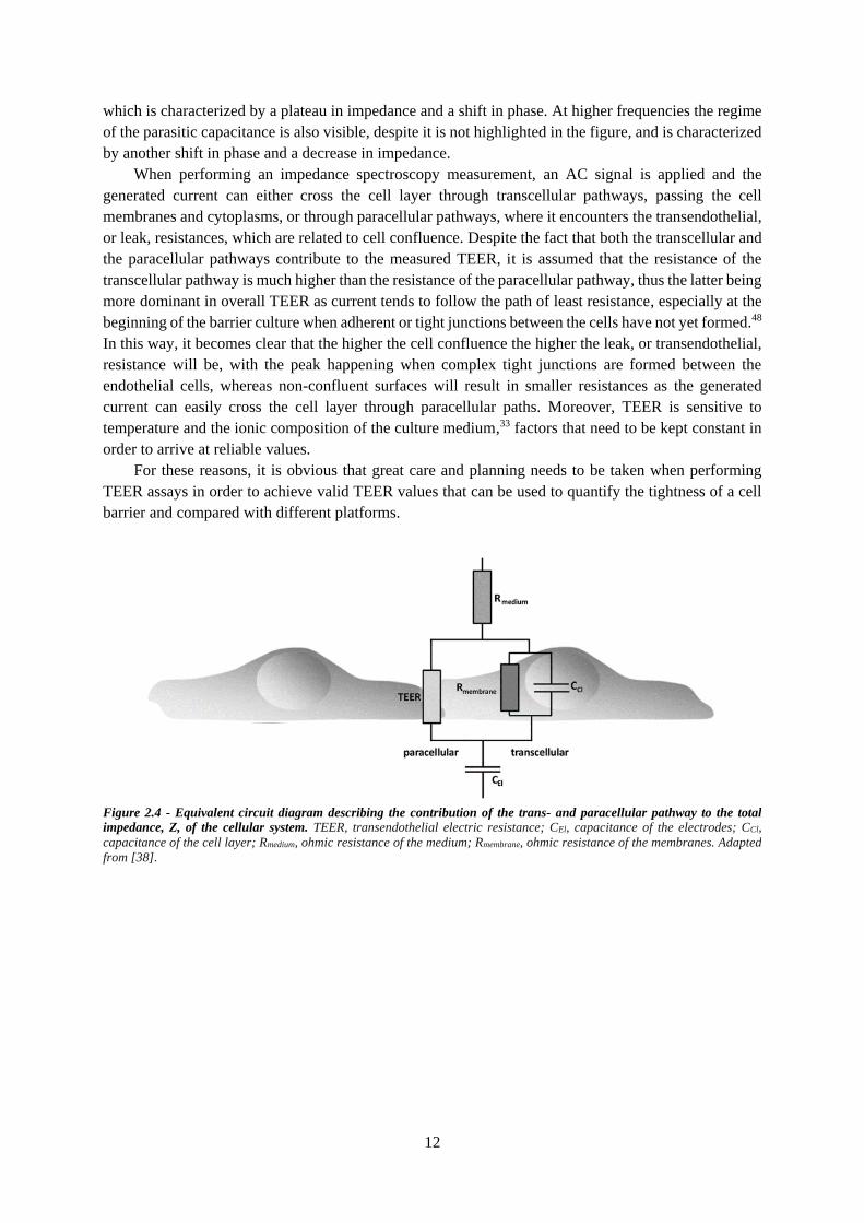
12
which is characterized by a plateau in impedance and a shift in phase. At higher frequencies the regime
of the parasitic capacitance is also visible, despite it is not highlighted in the figure, and is characterized
by another shift in phase and a decrease in impedance.
When performing an impedance spectroscopy measurement, an AC signal is applied and the
generated current can either cross the cell layer through transcellular pathways, passing the cell
membranes and cytoplasms, or through paracellular pathways, where it encounters the transendothelial,
or leak, resistances, which are related to cell confluence. Despite the fact that both the transcellular and
the paracellular pathways contribute to the measured TEER, it is assumed that the resistance of the
transcellular pathway is much higher than the resistance of the paracellular pathway, thus the latter being
more dominant in overall TEER as current tends to follow the path of least resistance, especially at the
beginning of the barrier culture when adherent or tight junctions between the cells have not yet formed.48
In this way, it becomes clear that the higher the cell confluence the higher the leak, or transendothelial,
resistance will be, with the peak happening when complex tight junctions are formed between the
endothelial cells, whereas non-confluent surfaces will result in smaller resistances as the generated
current can easily cross the cell layer through paracellular paths. Moreover, TEER is sensitive to
temperature and the ionic composition of the culture medium,33 factors that need to be kept constant in
order to arrive at reliable values.
For these reasons, it is obvious that great care and planning needs to be taken when performing
TEER assays in order to achieve valid TEER values that can be used to quantify the tightness of a cell
barrier and compared with different platforms.
Figure 2.4 - Equivalent circuit diagram describing the contribution of the trans- and paracellular pathway to the total
impedance, Z, of the cellular system. TEER, transendothelial electric resistance; CEl, capacitance of the electrodes; CCl,
capacitance of the cell layer; Rmedium, ohmic resistance of the medium; Rmembrane, ohmic resistance of the membranes. Adapted
from [38].
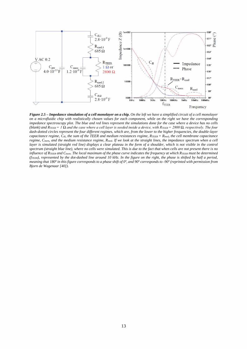
13
Figure 2.5 – Impedance simulation of a cell monolayer on a chip. On the left we have a simplified circuit of a cell monolayer
on a microfluidic chip with realistically chosen values for each component, while on the right we have the corresponding
impedance spectroscopy plot. The blue and red lines represent the simulations done for the case where a device has no cells
(blank) and RTEER = 1 Ω and the case where a cell layer is seeded inside a device, with RTEER = 2800 Ω, respectively. The four
dash-dotted circles represent the four different regimes, which are, from the lower to the higher frequencies, the double-layer
capacitance regime, Cdl, the sum of the TEER and medium resistances regime, RTEER + Rmed, the cell membrane capacitance
regime, Cmem, and the medium resistance regime, Rmed. If we look at the straight lines, the impedance spectrum when a cell
layer is simulated (straight red line) displays a clear plateau in the form of a shoulder, which is not visible in the control
spectrum (straight blue line), where no cells were simulated. This is due to the fact that when cells are not present there is no
influence of RTEER and Cmem. The local maximum of the phase curve indicates the frequency at which RTEER must be determined
(fTEER), represented by the dot-dashed line around 10 kHz. In the figure on the right, the phase is shifted by half a period,
meaning that 180º in this figure corresponds to a phase shift of 0º, and 90º corresponds to -90º (reprinted with permission from
Bjorn de Wagenaar [40]).
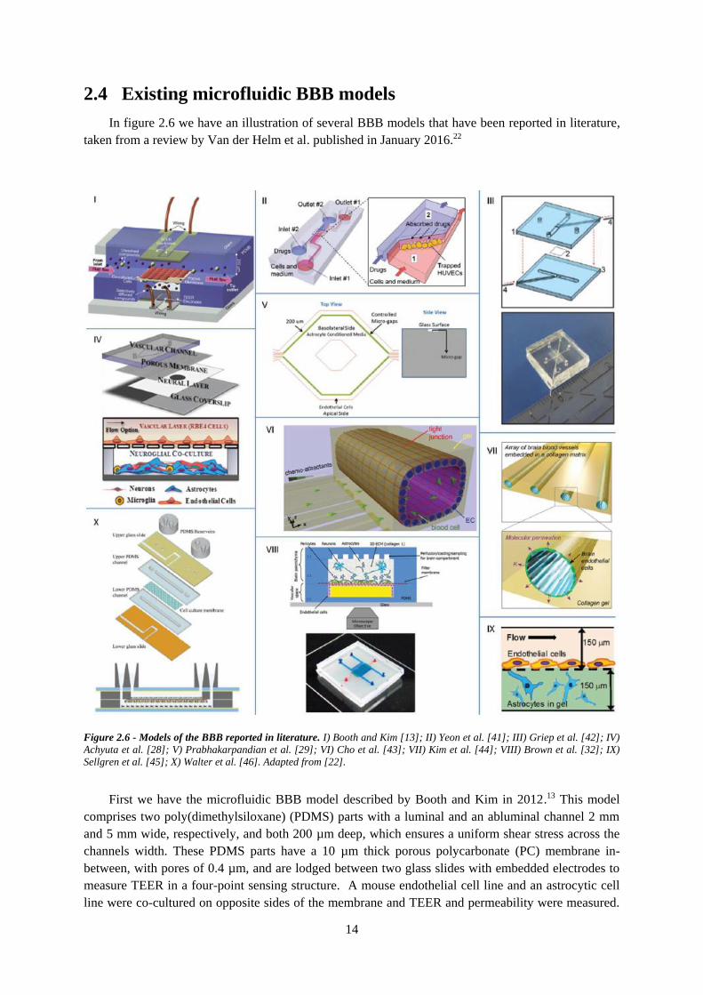
14
2.4 Existing microfluidic BBB models
In figure 2.6 we have an illustration of several BBB models that have been reported in literature,
taken from a review by Van der Helm et al. published in January 2016.22
First we have the microfluidic BBB model described by Booth and Kim in 2012.13 This model
comprises two poly(dimethylsiloxane) (PDMS) parts with a luminal and an abluminal channel 2 mm
and 5 mm wide, respectively, and both 200 µm deep, which ensures a uniform shear stress across the
channels width. These PDMS parts have a 10 µm thick porous polycarbonate (PC) membrane in-
between, with pores of 0.4 µm, and are lodged between two glass slides with embedded electrodes to
measure TEER in a four-point sensing structure. A mouse endothelial cell line and an astrocytic cell
line were co-cultured on opposite sides of the membrane and TEER and permeability were measured.
Figure 2.6 - Models of the BBB reported in literature. I) Booth and Kim [13]; II) Yeon et al. [41]; III) Griep et al. [42]; IV)
Achyuta et al. [28]; V) Prabhakarpandian et al. [29]; VI) Cho et al. [43]; VII) Kim et al. [44]; VIII) Brown et al. [32]; IX)
Sellgren et al. [45]; X) Walter et al. [46]. Adapted from [22].
15
Besides this, fluorescence staining of tight junctions was performed, and barrier exposure to histamine
was monitored. One of the drawbacks of this model is the fact that the electrodes on the glass slides
significantly reduce the cross-sectional area view.
Model II, described by Yeon et al. also in 2012,41 consists of two channels, 25 µm high, connected
by microholes in which human umbilical cord endothelial cells were trapped hydrodynamically by
applying a pressure difference between the channels. After a short incubation period (2-3 hours) it was
possible to observe tight junction formation in astrocyte-conditioned medium (ACM) and the transport
of small molecules and several drugs across the barrier was studied. The fact that there is the need to
maintain a stable pressure difference between the two channels in order to keep the cells trapped is one
of the drawbacks of this model.
Model III was reported by Griep et al. in 201342 and consists of two PDMS parts, both with 500
µm wide and 100 µm deep channels, glued together with a 10 µm thick PC membrane with 0.4 µm
diameter pores in-between. Other than that, to perform TEER measurements, two platinum electrodes
are placed 200 µm apart on each side of the membrane. In this model, human cerebral microvascular
endothelial cells were cultured on the top part of the membrane and after two days a functional barrier
was obtained.
Model IV, described by Achyuta et al. in 2013,28 consists of a neural and a vascular part that can
be fabricated and cultured separately. The neural part consists of a cover slip containing a 100 µm thick
PDMS layer with an 8 mm diameter hole, on which rat cortical cells were cultured. As for the vascular
part, it is a 10 mm wide and 100 µm high channel glued on a 7 µm thick porous PC membrane, with 8
µm diameter pores, on which rat brain endothelial cells were cultured. After the end of the culture period
both parts were assembled together and barrier tightness and function were assessed. Some drawbacks
of this model are the fact that there is no way to access the neural culture after assembly other than
through the vascular layer and TEER cannot be measured.
Model V was reported by Prabhakarpandian et al. also in 201329 and consists of a blood
compartment (outer ring with 200 µm width and 100 µm depth) and a brain compartment (inner ring)
connected to each other by micro gaps in a PDMS wall. These compartments are imprinted in a PDMS
part bonded to a glass slide and were designed in such a way to allow the simultaneous imaging of both
of them. In this model, a layer of cells perpendicular to the gaps was achieved by culturing rat brain
endothelial cells, under fluidic shear, in the blood compartment. In addition, astrocyte-conditioned
medium could be added to the brain compartment to promote tight junction formation and further
decrease barrier permeability. In order to assess the functionality of the model, permeation studies were
performed as well as analysis of protein expression and the reaction of endothelial cells to ACM. The
gaps on the side of the cell layer are a drawback of this model as they might allow cells to migrate to
the basolateral side of the chamber, thus increasing the risk of creating gaps in the barrier.
Model VI was published by Cho et al. in 201543 and consists of a PDMS part positioned between
two well plates, one of acrylic and the other of glass. The PDMS part comprises brain and endothelial
channels, both 50 µm high, which are connected by an array of small perpendicular channels (5 µm
high). The channels were first coated with poly-D-lysine and subsequently filled with a collagen I gel,
which was then replaced by cell culturing medium in the endothelial chambers, which resulted in a thin
layer of collagen gel on the walls. Rat endothelial cells were then cultured on the collagen and the barrier
function was evaluated after a cell monolayer was obtained. Besides this, the authors also simulated
barrier inflammation through the use of tumor necrosis factor alpha (TNF-α) and studied ischemia
conditions by depriving the endothelium of oxygen and glucose and subsequently reoxygenating it under
normal conditions.
Model VII was reported by Kim et al. in 201544 and consists of a collagen-based 3D model of the
BBB. In this model, a 3D frame, to which fluidic connectors can be coupled, was printed and collagen
I was poured around the microneedles placed in the square in the middle of the frame, which resulted in
16
235-360 µm diameter hollow tubes. After this, mouse brain-derived endothelial cells were cultured in
these tubes and 14 days later immunofluorescence showed intact vessels with tight junction protein ZO-
1 expression. Other than that, permeability assays were performed and permeability coefficients were
derived from fluorescence images of these assays. Furthermore, the authors also monitored barrier
exposure to mannitol.
Model VIII was described by Brown et al. in 201532 and it comprises three PDMS parts consisting
of a 100 µm high and 6.2 mm wide vascular compartment with inlet channels, a 4.75 mm wide, 6.2 mm
long and 500 µm deep brain compartment and several parallel channels (100 µm high), forming brain
perfusion channels. Moreover, there is a PC membrane with 0.2 µm diameter pores that separates the
vascular and brain compartments. The vascular compartment was held upside down and under constant
flow and primary human brain-derived microvascular endothelial cells (hBMVEC) were cultured on the
membrane. The device was flipped right-side up after 12 days and pericytes and astrocytes were cultured
in the brain compartment, which was filled with a collagen I matrix with suspended human induced
pluripotent stem cell-derived neurons two days after. Live/dead staining and immunofluorescence
staining were done to assess cell viability and the presence of tight junctions (ZO-1), respectively.
Moreover, the percentage of actin filaments that were aligned with the flow direction was quantified and
permeability assays and TEER measurements, using a 4-point impedance sensing method, were
performed.
Model IX was reported by Sellgren et al. in 201545 and comprises two PDMS parts with a
polytetrafluoroethylene (PTFE) or polyester (PE) membrane in-between. The vascular compartment was
10 mm long, 1 mm wide and 150 µm high, the basolateral compartment was 150-300 µm high and the
membrane had 0.4 µm pores and a thickness of 40 or 10 µm for PTFE or PE, respectively. A murine
cell line of astrocytes was suspended in a collagen hydrogel and cultured in the basolateral compartment
and a murine brain endothelial cell line was cultured on the vascular compartment under a fluid flow
that reproduced physiologically relevant shear stress. As both membranes were transparent, it was
possible to monitor the cell monolayer formation with phase contrast microscopy and when this
monolayer was formed, the collagen containing the astrocytes was flushed out and barrier function was
tested. Furthermore, the authors were able to conclude that the PTFE membranes were more suitable to
support cell attachment and relevant shear stress, as in this membrane the cell monolayer was able to
survive the shear stress caused by the fluid flow and immunofluorescence showed tight junction protein
claudin-5 expression and in the case of the PE membrane cells detached from the membrane due to the
flow and failed to show any tight junction expression.
Model X was published by Walter et al.46 and consists of two PDMS parts with imprinted channels
with heights and widths of 200 µm separated by a polyethylene terephthalate (PET) membrane with a
thickness of 23 µm and pores with a diameter of 0.45 µm. These PDMS parts are fixated to each other
with a silicone sealant and placed between two glass slides with sputtered 25 nm thick transparent gold
electrodes, which are positioned in a four-point sensing structure to measure TEER at near-DC
conditions. Moreover, the top glass slide is attached to two PDMS reservoirs by plasma-bonding,
through which the cells are seeded. Endothelial cells, either human or rat types, were cultured in the top
side of the membrane in the top channel, pericytes in the bottom side of the membrane and astrocytes
on the bottom of the bottom channel. The permeability of the barrier was measured statically by
determining the concentration in the brain compartment at different time intervals and confocal
microscopy was used to assess the presence of both tight junction and adherens junction proteins. In
addition, this model was also used to recreate the intestinal and lung epithelial barriers.

17
2.5 Summary
As explained in the previous sections, the need for a multiplexed platform with high-throughput
that allows several experimental conditions to be created at the same time in the same device is clear. In
organs-on-chips, the two main ways to address this are the 2D, membrane-based, and the 3D, gel-based,
systems. However, and to more closely mimic the physiologically relevance and functionality of the
BBB, several aspects need to be taken into consideration when developing such platforms. Among the
most important are whether the model will enable the formation of endothelial cell barriers with BBB
morphology, such as AJs and TJs formation, and whether it can integrate important tests that allow the
monitoring of the functionality of the barrier, such as permeability and TEER analysis. Besides these,
and in what concerns the design of the platform, there are some considerations which also have to be
taken into account, being one of the most important the dimensions of its microfluidic chambers. With
all these aspects in mind, two different models of the BBB, a 2D and a 3D, were designed, developed,
thoroughly characterized and will now be fully described.

18
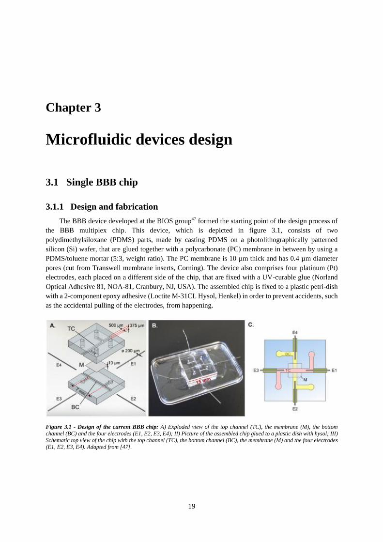
19
Chapter 3
Microfluidic devices design
3.1 Single BBB chip
3.1.1 Design and fabrication
The BBB device developed at the BIOS group47 formed the starting point of the design process of
the BBB multiplex chip. This device, which is depicted in figure 3.1, consists of two
polydimethylsiloxane (PDMS) parts, made by casting PDMS on a photolithographically patterned
silicon (Si) wafer, that are glued together with a polycarbonate (PC) membrane in between by using a
PDMS/toluene mortar (5:3, weight ratio). The PC membrane is 10 µm thick and has 0.4 µm diameter
pores (cut from Transwell membrane inserts, Corning). The device also comprises four platinum (Pt)
electrodes, each placed on a different side of the chip, that are fixed with a UV-curable glue (Norland
Optical Adhesive 81, NOA-81, Cranbury, NJ, USA). The assembled chip is fixed to a plastic petri-dish
with a 2-component epoxy adhesive (Loctite M-31CL Hysol, Henkel) in order to prevent accidents, such
as the accidental pulling of the electrodes, from happening.
Figure 3.1 - Design of the current BBB chip: A) Exploded view of the top channel (TC), the membrane (M), the bottom
channel (BC) and the four electrodes (E1, E2, E3, E4); II) Picture of the assembled chip glued to a plastic dish with hysol; III)
Schematic top view of the chip with the top channel (TC), the bottom channel (BC), the membrane (M) and the four electrodes
(E1, E2, E3, E4). Adapted from [47].
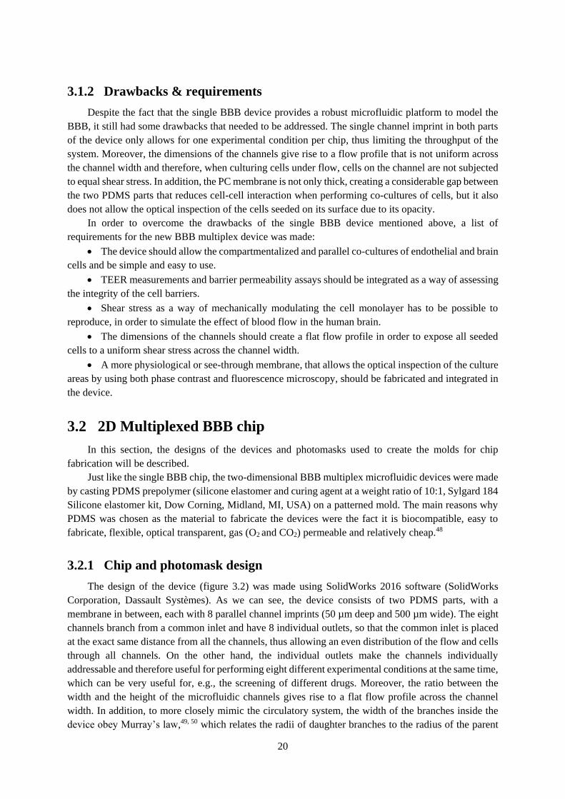
20
3.1.2 Drawbacks & requirements
Despite the fact that the single BBB device provides a robust microfluidic platform to model the
BBB, it still had some drawbacks that needed to be addressed. The single channel imprint in both parts
of the device only allows for one experimental condition per chip, thus limiting the throughput of the
system. Moreover, the dimensions of the channels give rise to a flow profile that is not uniform across
the channel width and therefore, when culturing cells under flow, cells on the channel are not subjected
to equal shear stress. In addition, the PC membrane is not only thick, creating a considerable gap between
the two PDMS parts that reduces cell-cell interaction when performing co-cultures of cells, but it also
does not allow the optical inspection of the cells seeded on its surface due to its opacity.
In order to overcome the drawbacks of the single BBB device mentioned above, a list of
requirements for the new BBB multiplex device was made:
The device should allow the compartmentalized and parallel co-cultures of endothelial and brain
cells and be simple and easy to use.
TEER measurements and barrier permeability assays should be integrated as a way of assessing
the integrity of the cell barriers.
Shear stress as a way of mechanically modulating the cell monolayer has to be possible to
reproduce, in order to simulate the effect of blood flow in the human brain.
The dimensions of the channels should create a flat flow profile in order to expose all seeded
cells to a uniform shear stress across the channel width.
A more physiological or see-through membrane, that allows the optical inspection of the culture
areas by using both phase contrast and fluorescence microscopy, should be fabricated and integrated in
the device.
3.2 2D Multiplexed BBB chip
In this section, the designs of the devices and photomasks used to create the molds for chip
fabrication will be described.
Just like the single BBB chip, the two-dimensional BBB multiplex microfluidic devices were made
by casting PDMS prepolymer (silicone elastomer and curing agent at a weight ratio of 10:1, Sylgard 184
Silicone elastomer kit, Dow Corning, Midland, MI, USA) on a patterned mold. The main reasons why
PDMS was chosen as the material to fabricate the devices were the fact it is biocompatible, easy to
fabricate, flexible, optical transparent, gas (O2 and CO2) permeable and relatively cheap.48
3.2.1 Chip and photomask design
The design of the device (figure 3.2) was made using SolidWorks 2016 software (SolidWorks
Corporation, Dassault Systèmes). As we can see, the device consists of two PDMS parts, with a
membrane in between, each with 8 parallel channel imprints (50 µm deep and 500 µm wide). The eight
channels branch from a common inlet and have 8 individual outlets, so that the common inlet is placed
at the exact same distance from all the channels, thus allowing an even distribution of the flow and cells
through all channels. On the other hand, the individual outlets make the channels individually
addressable and therefore useful for performing eight different experimental conditions at the same time,
which can be very useful for, e.g., the screening of different drugs. Moreover, the ratio between the
width and the height of the microfluidic channels gives rise to a flat flow profile across the channel
width. In addition, to more closely mimic the circulatory system, the width of the branches inside the
device obey Murray’s law,49, 50 which relates the radii of daughter branches to the radius of the parent
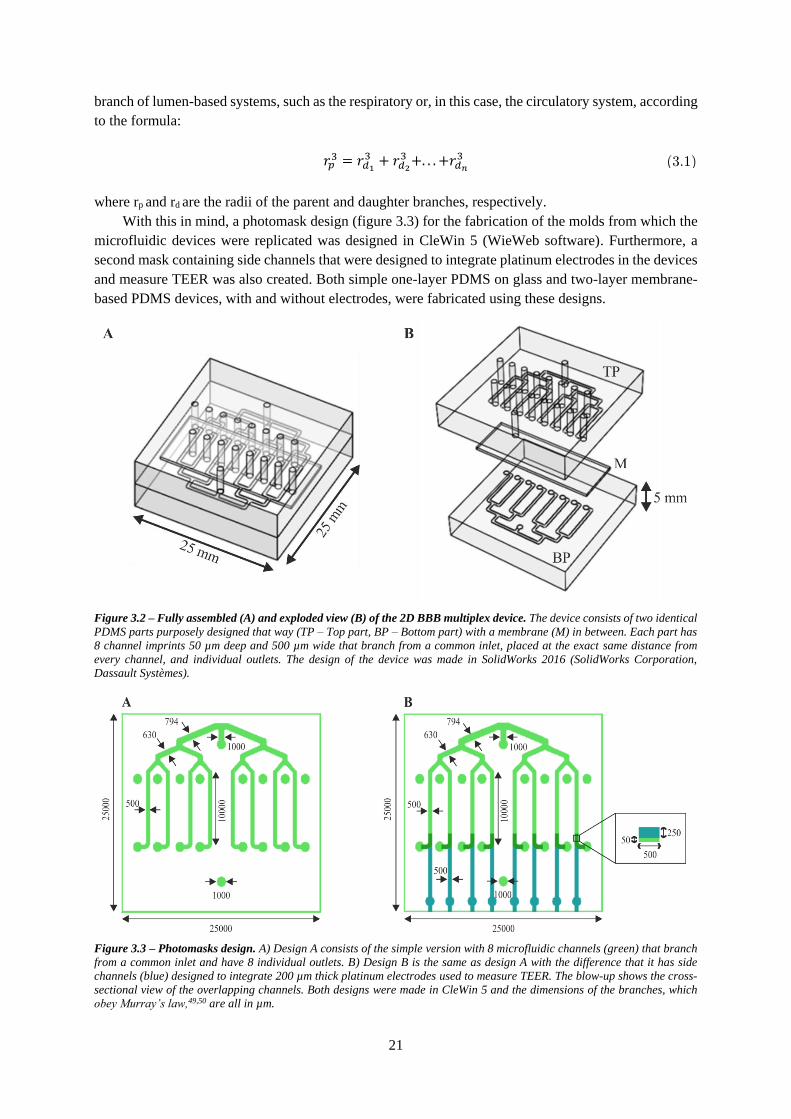
21
branch of lumen-based systems, such as the respiratory or, in this case, the circulatory system, according
to the formula:
𝑟𝑝3 = 𝑟𝑑1
3 + 𝑟𝑑2
3 +. . . +𝑟𝑑𝑛
3
where rp and rd are the radii of the parent and daughter branches, respectively.
With this in mind, a photomask design (figure 3.3) for the fabrication of the molds from which the
microfluidic devices were replicated was designed in CleWin 5 (WieWeb software). Furthermore, a
second mask containing side channels that were designed to integrate platinum electrodes in the devices
and measure TEER was also created. Both simple one-layer PDMS on glass and two-layer membrane-
based PDMS devices, with and without electrodes, were fabricated using these designs.
(3.1)
Figure 3.2 – Fully assembled (A) and exploded view (B) of the 2D BBB multiplex device. The device consists of two identical
PDMS parts purposely designed that way (TP – Top part, BP – Bottom part) with a membrane (M) in between. Each part has
8 channel imprints 50 µm deep and 500 µm wide that branch from a common inlet, placed at the exact same distance from
every channel, and individual outlets. The design of the device was made in SolidWorks 2016 (SolidWorks Corporation,
Dassault Systèmes).
Figure 3.3 – Photomasks design. A) Design A consists of the simple version with 8 microfluidic channels (green) that branch
from a common inlet and have 8 individual outlets. B) Design B is the same as design A with the difference that it has side
channels (blue) designed to integrate 200 µm thick platinum electrodes used to measure TEER. The blow-up shows the cross-
sectional view of the overlapping channels. Both designs were made in CleWin 5 and the dimensions of the branches, which
obey Murray’s law,49,50 are all in µm.
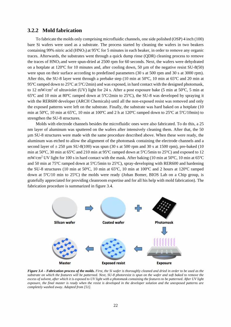
22
3.2.2 Mold fabrication
To fabricate the molds only comprising microfluidic channels, one side polished (OSP) 4 inch (100)
bare Si wafers were used as a substrate. The process started by cleaning the wafers in two beakers
containing 99% nitric acid (HNO3) at 95ºC for 5 minutes in each beaker, in order to remove any organic
traces. Afterwards, the substrates went through a quick dump rinse (QDR) cleaning process to remove
the traces of HNO3 and were spun-dried at 2500 rpm for 60 seconds. Next, the wafers were dehydrated
on a hotplate at 120ºC for 10 minutes and, after cooling down, 50 µm of the negative resist SU-8(50)
were spun on their surface according to predefined parameters (30 s at 500 rpm and 30 s at 3000 rpm).
After this, the SU-8 layer went through a prebake step (10 min at 50ºC, 10 min at 65ºC and 20 min at
95ºC ramped down to 25ºC at 5ºC/2min) and was exposed, in hard contact with the designed photomask,
to 12 mW/cm2 of ultraviolet (UV) light for 24 s. After a post exposure bake (5 min at 50ºC, 5 min at
65ºC and 10 min at 80ºC ramped down at 5ºC/2min to 25ºC), the SU-8 was developed by spraying it
with the RER600 developer (ARCH Chemicals) until all the non-exposed resist was removed and only
the exposed patterns were left on the substrate. Finally, the substrate was hard baked on a hotplate (10
min at 50ºC, 10 min at 65ºC, 10 min at 100ºC and 2 h at 120ºC ramped down to 25ºC at 5ºC/10min) to
strengthen the SU-8 structures.
Molds with electrode channels besides the microfluidic ones were also fabricated. To do this, a 25
nm layer of aluminum was sputtered on the wafers after intensively cleaning them. After that, the 50
µm SU-8 structures were made with the same procedure described above. When these were ready, the
aluminum was etched to allow the alignment of the photomask containing the electrode channels and a
second layer of ± 250 µm SU-8(100) was spun (30 s at 500 rpm and 30 s at 1500 rpm), pre-baked (10
min at 50ºC, 30 min at 65ºC and 210 min at 95ºC ramped down at 5ºC/5min to 25ºC) and exposed to 12
mW/cm2 UV light for 100 s in hard contact with the mask. After baking (10 min at 50ºC, 10 min at 65ºC
and 50 min at 75ºC ramped down at 5ºC/5min to 25ºC), spray-developing with RER600 and hardening
the SU-8 structures (10 min at 50ºC, 10 min at 65ºC, 10 min at 100ºC and 2 hours at 120ºC ramped
down at 5ºC/10 min to 25ºC) the molds were ready (Johan Bomer, BIOS Lab on a Chip group, is
gratefully appreciated for providing cleanroom expertise and for all his help with mold fabrication). The
fabrication procedure is summarized in figure 3.4.
Figure 3.4 – Fabrication process of the molds. First, the Si wafer is thoroughly cleaned and dried in order to be used as the
substrate on which the features will be patterned. Next, SU-8 photoresist is spun on the wafer and soft baked to remove the
excess of solvent, after which it is exposed to UV light with a photomask containing the features to be patterned. After UV light
exposure, the final master is ready when the resist is developed in the developer solution and the unexposed patterns are
completely washed away. Adapted from [51].
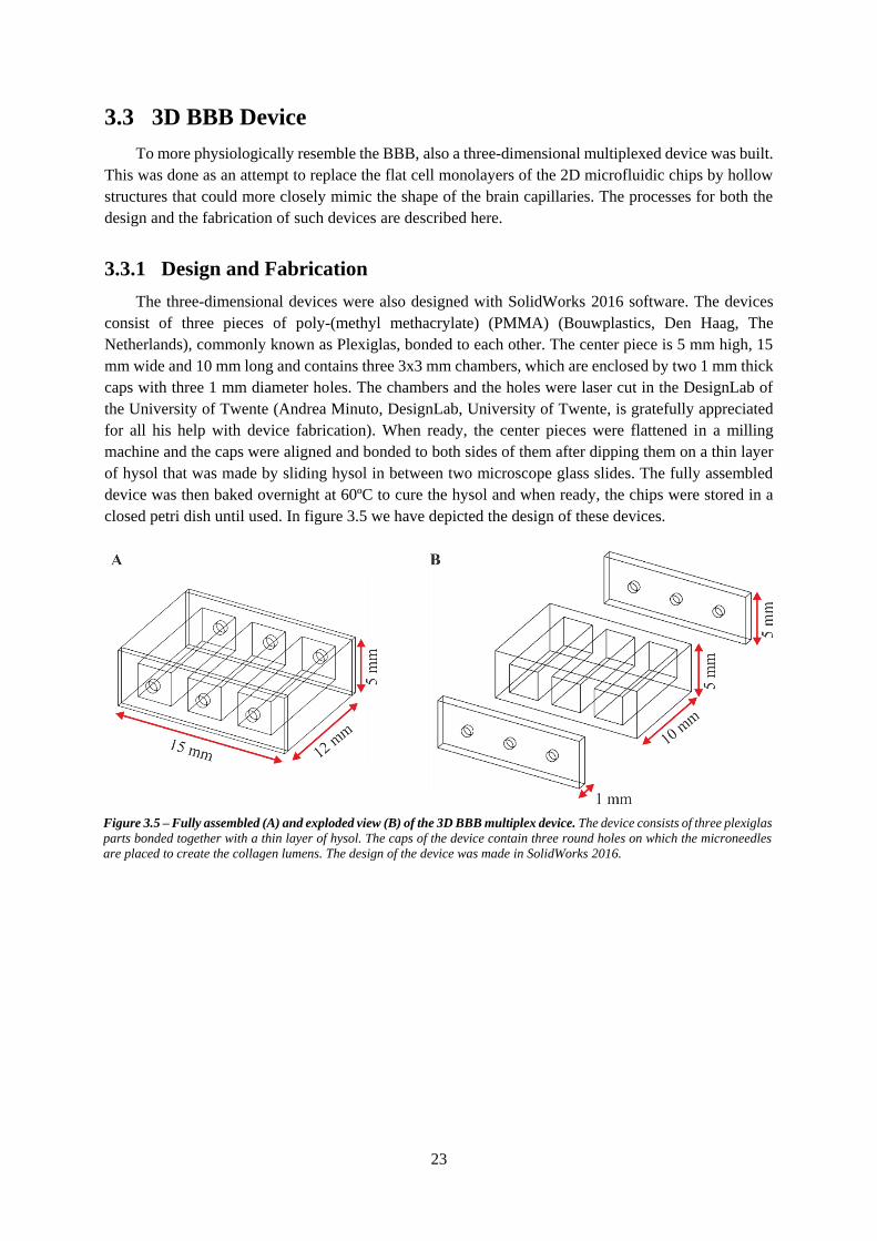
23
3.3 3D BBB Device
To more physiologically resemble the BBB, also a three-dimensional multiplexed device was built.
This was done as an attempt to replace the flat cell monolayers of the 2D microfluidic chips by hollow
structures that could more closely mimic the shape of the brain capillaries. The processes for both the
design and the fabrication of such devices are described here.
3.3.1 Design and Fabrication
The three-dimensional devices were also designed with SolidWorks 2016 software. The devices
consist of three pieces of poly-(methyl methacrylate) (PMMA) (Bouwplastics, Den Haag, The
Netherlands), commonly known as Plexiglas, bonded to each other. The center piece is 5 mm high, 15
mm wide and 10 mm long and contains three 3x3 mm chambers, which are enclosed by two 1 mm thick
caps with three 1 mm diameter holes. The chambers and the holes were laser cut in the DesignLab of
the University of Twente (Andrea Minuto, DesignLab, University of Twente, is gratefully appreciated
for all his help with device fabrication). When ready, the center pieces were flattened in a milling
machine and the caps were aligned and bonded to both sides of them after dipping them on a thin layer
of hysol that was made by sliding hysol in between two microscope glass slides. The fully assembled
device was then baked overnight at 60ºC to cure the hysol and when ready, the chips were stored in a
closed petri dish until used. In figure 3.5 we have depicted the design of these devices.
Figure 3.5 – Fully assembled (A) and exploded view (B) of the 3D BBB multiplex device. The device consists of three plexiglas
parts bonded together with a thin layer of hysol. The caps of the device contain three round holes on which the microneedles
are placed to create the collagen lumens. The design of the device was made in SolidWorks 2016.

24
25
Chapter 4
Membrane fabrication
As was mentioned before, the opacity and the thickness of the PC membrane used in the BBB
device inhibit the monitoring of the cells by normal light microscopy and create a considerable gap
between the endothelial and brain cells when in co-culture, reducing cell-cell interaction. Moreover, the
gluing process of these membranes in between the PDMS parts was quite challenging and time
consuming, as will be explained further, especially in the BBB multiplex device due to its shallow
channels. For these reasons, it was decided to improve the membrane of the BBB device and polystyrene
(PS), Silicon-rich nitride (SiRN) and PDMS membranes were fabricated.
4.1 Methods
4.1.1 Polystyrene membrane
To fabricate PS membranes, a solution containing 5% PS (Sigma Aldrich) in dichloromethane
(Sigma Aldrich) was used. The solution was stirred on a stirring plate, with the aid of a magnet, at 60-
80 rpm, and when PS was completely dissolved it was cast in 50 mm diameter Teflon dishes (Anne
Leferink, BIOS Lab on a Chip group, is greatly appreciated for providing the materials and the know-
how for PS membrane fabrication). The dishes were then placed under nitrogen (N2) purge to uniformly
harden the membranes and, when hardened, the membranes were carefully peeled from the dishes, using
a metal scalpel, and characterized.
4.1.2 Silicon-rich nitride membrane
Porous SiRN membranes were fabricated in the cleanroom facilities of the University of Twente
Nanolab (Johan Bomer, Wesley van den Beld and Hai Le The, BIOS Lab on a Chip group, are greatly
appreciated for all the provided help in fabricating SiRN membranes). The process started by cleaning
two OSP 4 inch (100) silicon wafers in two beakers containing 99% HNO3 (5 min each) to remove any
traces of organic materials. When cleaned, the substrates went through a QDR process to remove any
traces of chemical agents and then put in a beaker containing 69% HNO3 at 95ºC to remove metallic
traces. After 10 min inside the beaker, the substrates went through another QDR step, after which they
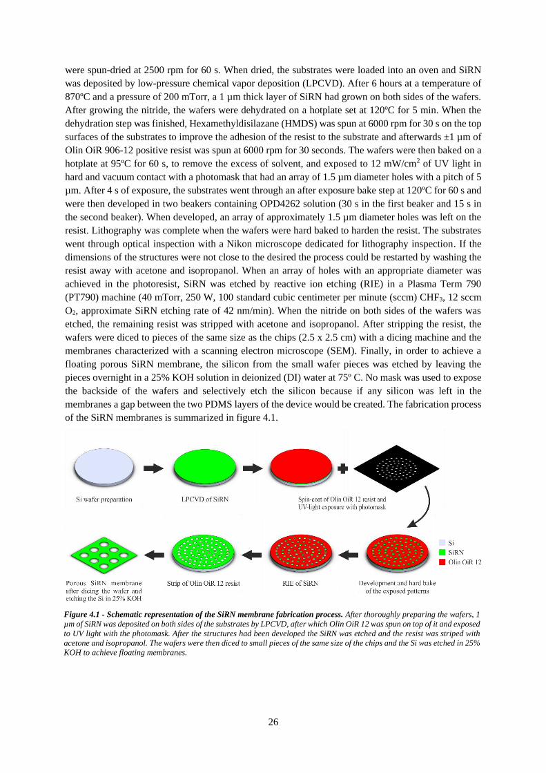
26
were spun-dried at 2500 rpm for 60 s. When dried, the substrates were loaded into an oven and SiRN
was deposited by low-pressure chemical vapor deposition (LPCVD). After 6 hours at a temperature of
870ºC and a pressure of 200 mTorr, a 1 µm thick layer of SiRN had grown on both sides of the wafers.
After growing the nitride, the wafers were dehydrated on a hotplate set at 120ºC for 5 min. When the
dehydration step was finished, Hexamethyldisilazane (HMDS) was spun at 6000 rpm for 30 s on the top
surfaces of the substrates to improve the adhesion of the resist to the substrate and afterwards ±1 µm of
Olin OiR 906-12 positive resist was spun at 6000 rpm for 30 seconds. The wafers were then baked on a
hotplate at 95ºC for 60 s, to remove the excess of solvent, and exposed to 12 mW/cm2 of UV light in
hard and vacuum contact with a photomask that had an array of 1.5 µm diameter holes with a pitch of 5
µm. After 4 s of exposure, the substrates went through an after exposure bake step at 120ºC for 60 s and
were then developed in two beakers containing OPD4262 solution (30 s in the first beaker and 15 s in
the second beaker). When developed, an array of approximately 1.5 µm diameter holes was left on the
resist. Lithography was complete when the wafers were hard baked to harden the resist. The substrates
went through optical inspection with a Nikon microscope dedicated for lithography inspection. If the
dimensions of the structures were not close to the desired the process could be restarted by washing the
resist away with acetone and isopropanol. When an array of holes with an appropriate diameter was
achieved in the photoresist, SiRN was etched by reactive ion etching (RIE) in a Plasma Term 790
(PT790) machine (40 mTorr, 250 W, 100 standard cubic centimeter per minute (sccm) CHF3, 12 sccm
O2, approximate SiRN etching rate of 42 nm/min). When the nitride on both sides of the wafers was
etched, the remaining resist was stripped with acetone and isopropanol. After stripping the resist, the
wafers were diced to pieces of the same size as the chips (2.5 x 2.5 cm) with a dicing machine and the
membranes characterized with a scanning electron microscope (SEM). Finally, in order to achieve a
floating porous SiRN membrane, the silicon from the small wafer pieces was etched by leaving the
pieces overnight in a 25% KOH solution in deionized (DI) water at 75º C. No mask was used to expose
the backside of the wafers and selectively etch the silicon because if any silicon was left in the
membranes a gap between the two PDMS layers of the device would be created. The fabrication process
of the SiRN membranes is summarized in figure 4.1.
Figure 4.1 - Schematic representation of the SiRN membrane fabrication process. After thoroughly preparing the wafers, 1
µm of SiRN was deposited on both sides of the substrates by LPCVD, after which Olin OiR 12 was spun on top of it and exposed
to UV light with the photomask. After the structures had been developed the SiRN was etched and the resist was striped with
acetone and isopropanol. The wafers were then diced to small pieces of the same size of the chips and the Si was etched in 25%
KOH to achieve floating membranes.
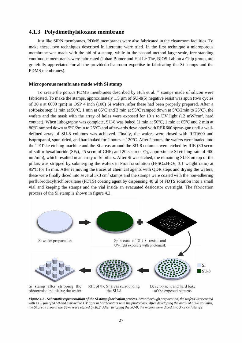
27
4.1.3 Polydimethylsiloxane membrane
Just like SiRN membranes, PDMS membranes were also fabricated in the cleanroom facilities. To
make these, two techniques described in literature were tried. In the first technique a microporous
membrane was made with the aid of a stamp, while in the second method large-scale, free-standing
continuous membranes were fabricated (Johan Bomer and Hai Le The, BIOS Lab on a Chip group, are
gratefully appreciated for all the provided cleanroom expertise in fabricating the Si stamps and the
PDMS membranes).
Microporous membrane made with Si stamp
To create the porous PDMS membranes described by Huh et al.,52 stamps made of silicon were
fabricated. To make the stamps, approximately 1.5 µm of SU-8(5) negative resist was spun (two cycles
of 30 s at 6000 rpm) in OSP 4 inch (100) Si wafers, after these had been properly prepared. After a
softbake step (1 min at 50ºC, 1 min at 65ºC and 3 min at 95ºC ramped down at 5ºC/2min to 25ºC), the
wafers and the mask with the array of holes were exposed for 10 s to UV light (12 mW/cm2, hard
contact). When lithography was complete, SU-8 was baked (1 min at 50ºC, 1 min at 65ºC and 2 min at
80ºC ramped down at 5ºC/2min to 25ºC) and afterwards developed with RER600 spray-gun until a well-
defined array of SU-8 columns was achieved. Finally, the wafers were rinsed with RER600 and
isopropanol, spun-dried, and hard baked for 2 hours at 120ºC. After 2 hours, the wafers were loaded into
the TETske etching machine and the Si areas around the SU-8 columns were etched by RIE (30 sccm
of sulfur hexafluoride (SF6), 25 sccm of CHF3 and 20 sccm of O2, approximate Si etching rate of 400
nm/min), which resulted in an array of Si pillars. After Si was etched, the remaining SU-8 on top of the
pillars was stripped by submerging the wafers in Piranha solution (H2SO4:H2O2, 3:1 weight ratio) at
95ºC for 15 min. After removing the traces of chemical agents with QDR steps and drying the wafers,
these were finally diced into several 3x3 cm2 stamps and the stamps were coated with the non-adhering
perfluorodecyltrichlorosilane (FDTS) coating agent by dispensing 40 µl of FDTS solution into a small
vial and keeping the stamps and the vial inside an evacuated desiccator overnight. The fabrication
process of the Si stamp is shown in figure 4.2.
Figure 4.2 - Schematic representation of the Si stamp fabrication process. After thorough preparation, the wafers were coated
with ±1.5 µm of SU-8 and exposed to UV light in hard contact with the photomask. After developing the array of SU-8 columns,
the Si areas around the SU-8 were etched by RIE. After stripping the SU-8, the wafers were diced into 3×3 cm2 stamps.
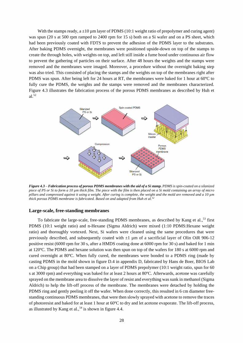
28
With the stamps ready, a ±10 µm layer of PDMS (10:1 weight ratio of prepolymer and curing agent)
was spun (20 s at 500 rpm ramped to 2400 rpm for 15 s) both on a Si wafer and on a PS sheet, which
had been previously coated with FDTS to prevent the adhesion of the PDMS layer to the substrates.
After baking PDMS overnight, the membranes were positioned upside-down on top of the stamps to
create the through holes, with weights on top, and left still inside a fume hood under continuous air flow
to prevent the gathering of particles on their surface. After 48 hours the weights and the stamps were
removed and the membranes were imaged. Moreover, a procedure without the overnight baking step
was also tried. This consisted of placing the stamps and the weights on top of the membranes right after
PDMS was spun. After being left for 24 hours at RT, the membranes were baked for 1 hour at 60ºC to
fully cure the PDMS, the weights and the stamps were removed and the membranes characterized.
Figure 4.3 illustrates the fabrication process of the porous PDMS membranes as described by Huh et
al.52
Large-scale, free-standing membranes
To fabricate the large-scale, free-standing PDMS membranes, as described by Kang et al.,53 first
PDMS (10:1 weight ratio) and n-Hexane (Sigma Aldrich) were mixed (1:10 PDMS:Hexane weight
ratio) and thoroughly vortexed. Next, Si wafers were cleaned using the same procedures that were
previously described, and subsequently coated with ±1 µm of a sacrificial layer of Olin OiR 906-12
positive resist (6000 rpm for 30 s, after a HMDS coating done at 6000 rpm for 30 s) and baked for 1 min
at 120ºC. The PDMS and hexane solution was then spun on top of the wafers for 180 s at 6000 rpm and
cured overnight at 80ºC. When fully cured, the membranes were bonded to a PDMS ring (made by
casting PDMS in the mold shown in figure D.4 in appendix D, fabricated by Hans de Boer, BIOS Lab
on a Chip group) that had been stamped on a layer of PDMS prepolymer (10:1 weight ratio, spun for 60
s at 3000 rpm) and everything was baked for at least 2 hours at 80ºC. Afterwards, acetone was carefully
sprayed on the membrane area to dissolve the layer of resist and everything was sunk in methanol (Sigma
Aldrich) to help the lift-off process of the membrane. The membranes were detached by holding the
PDMS ring and gently peeling it off the wafer. When done correctly, this resulted in 6 cm diameter free-
standing continuous PDMS membranes, that were then slowly sprayed with acetone to remove the traces
of photoresist and baked for at least 1 hour at 60ºC to dry and let acetone evaporate. The lift-off process,
as illustrated by Kang et al.,54 is shown in figure 4.4.
Figure 4.3 – Fabrication process of porous PDMS membranes with the aid of a Si stamp. PDMS is spin-coated on a silanized
piece of PS or Si to form a 10 µm thick film. The piece with the film is then placed on a Si mold containing an array of micro
pillars and compressed against it using a weight. After curing is complete, the weight and the mold are removed and a 10 µm
thick porous PDMS membrane is fabricated. Based on and adapted from Huh et al.52
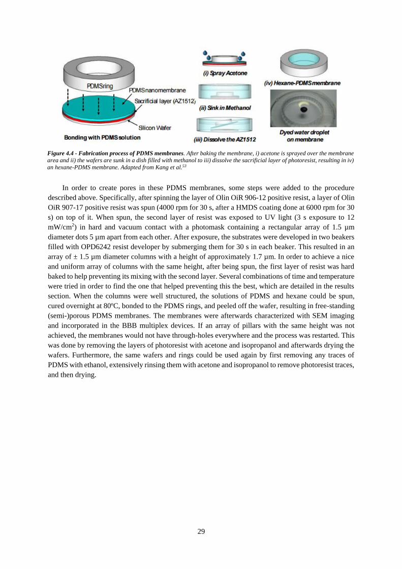
29
In order to create pores in these PDMS membranes, some steps were added to the procedure
described above. Specifically, after spinning the layer of Olin OiR 906-12 positive resist, a layer of Olin
OiR 907-17 positive resist was spun (4000 rpm for 30 s, after a HMDS coating done at 6000 rpm for 30
s) on top of it. When spun, the second layer of resist was exposed to UV light (3 s exposure to 12
mW/cm2) in hard and vacuum contact with a photomask containing a rectangular array of 1.5 µm
diameter dots 5 µm apart from each other. After exposure, the substrates were developed in two beakers
filled with OPD6242 resist developer by submerging them for 30 s in each beaker. This resulted in an
array of ± 1.5 µm diameter columns with a height of approximately 1.7 µm. In order to achieve a nice
and uniform array of columns with the same height, after being spun, the first layer of resist was hard
baked to help preventing its mixing with the second layer. Several combinations of time and temperature
were tried in order to find the one that helped preventing this the best, which are detailed in the results
section. When the columns were well structured, the solutions of PDMS and hexane could be spun,
cured overnight at 80ºC, bonded to the PDMS rings, and peeled off the wafer, resulting in free-standing
(semi-)porous PDMS membranes. The membranes were afterwards characterized with SEM imaging
and incorporated in the BBB multiplex devices. If an array of pillars with the same height was not
achieved, the membranes would not have through-holes everywhere and the process was restarted. This
was done by removing the layers of photoresist with acetone and isopropanol and afterwards drying the
wafers. Furthermore, the same wafers and rings could be used again by first removing any traces of
PDMS with ethanol, extensively rinsing them with acetone and isopropanol to remove photoresist traces,
and then drying.
Figure 4.4 - Fabrication process of PDMS membranes. After baking the membrane, i) acetone is sprayed over the membrane
area and ii) the wafers are sunk in a dish filled with methanol to iii) dissolve the sacrificial layer of photoresist, resulting in iv)
an hexane-PDMS membrane. Adapted from Kang et al.53
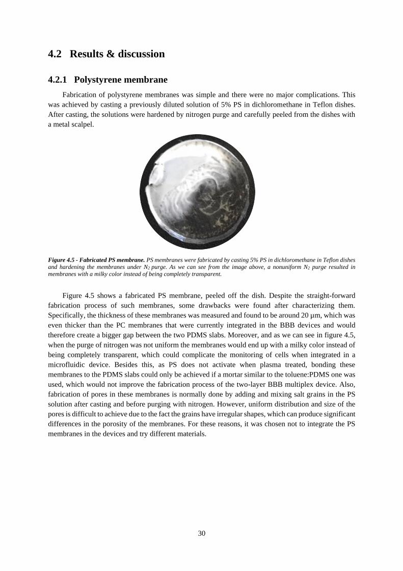
30
4.2 Results & discussion
4.2.1 Polystyrene membrane
Fabrication of polystyrene membranes was simple and there were no major complications. This
was achieved by casting a previously diluted solution of 5% PS in dichloromethane in Teflon dishes.
After casting, the solutions were hardened by nitrogen purge and carefully peeled from the dishes with
a metal scalpel.
Figure 4.5 shows a fabricated PS membrane, peeled off the dish. Despite the straight-forward
fabrication process of such membranes, some drawbacks were found after characterizing them.
Specifically, the thickness of these membranes was measured and found to be around 20 µm, which was
even thicker than the PC membranes that were currently integrated in the BBB devices and would
therefore create a bigger gap between the two PDMS slabs. Moreover, and as we can see in figure 4.5,
when the purge of nitrogen was not uniform the membranes would end up with a milky color instead of
being completely transparent, which could complicate the monitoring of cells when integrated in a
microfluidic device. Besides this, as PS does not activate when plasma treated, bonding these
membranes to the PDMS slabs could only be achieved if a mortar similar to the toluene:PDMS one was
used, which would not improve the fabrication process of the two-layer BBB multiplex device. Also,
fabrication of pores in these membranes is normally done by adding and mixing salt grains in the PS
solution after casting and before purging with nitrogen. However, uniform distribution and size of the
pores is difficult to achieve due to the fact the grains have irregular shapes, which can produce significant
differences in the porosity of the membranes. For these reasons, it was chosen not to integrate the PS
membranes in the devices and try different materials.
Figure 4.5 - Fabricated PS membrane. PS membranes were fabricated by casting 5% PS in dichloromethane in Teflon dishes
and hardening the membranes under N2 purge. As we can see from the image above, a nonuniform N2 purge resulted in
membranes with a milky color instead of being completely transparent.
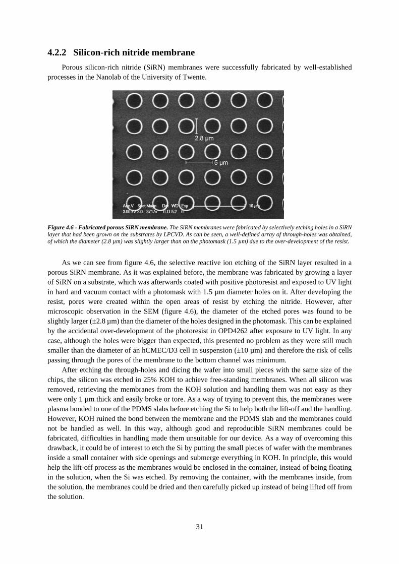
31
4.2.2 Silicon-rich nitride membrane
Porous silicon-rich nitride (SiRN) membranes were successfully fabricated by well-established
processes in the Nanolab of the University of Twente.
As we can see from figure 4.6, the selective reactive ion etching of the SiRN layer resulted in a
porous SiRN membrane. As it was explained before, the membrane was fabricated by growing a layer
of SiRN on a substrate, which was afterwards coated with positive photoresist and exposed to UV light
in hard and vacuum contact with a photomask with 1.5 µm diameter holes on it. After developing the
resist, pores were created within the open areas of resist by etching the nitride. However, after
microscopic observation in the SEM (figure 4.6), the diameter of the etched pores was found to be
slightly larger (±2.8 µm) than the diameter of the holes designed in the photomask. This can be explained
by the accidental over-development of the photoresist in OPD4262 after exposure to UV light. In any
case, although the holes were bigger than expected, this presented no problem as they were still much
smaller than the diameter of an hCMEC/D3 cell in suspension (±10 µm) and therefore the risk of cells
passing through the pores of the membrane to the bottom channel was minimum.
After etching the through-holes and dicing the wafer into small pieces with the same size of the
chips, the silicon was etched in 25% KOH to achieve free-standing membranes. When all silicon was
removed, retrieving the membranes from the KOH solution and handling them was not easy as they
were only 1 µm thick and easily broke or tore. As a way of trying to prevent this, the membranes were
plasma bonded to one of the PDMS slabs before etching the Si to help both the lift-off and the handling.
However, KOH ruined the bond between the membrane and the PDMS slab and the membranes could
not be handled as well. In this way, although good and reproducible SiRN membranes could be
fabricated, difficulties in handling made them unsuitable for our device. As a way of overcoming this
drawback, it could be of interest to etch the Si by putting the small pieces of wafer with the membranes
inside a small container with side openings and submerge everything in KOH. In principle, this would
help the lift-off process as the membranes would be enclosed in the container, instead of being floating
in the solution, when the Si was etched. By removing the container, with the membranes inside, from
the solution, the membranes could be dried and then carefully picked up instead of being lifted off from
the solution.
Figure 4.6 - Fabricated porous SiRN membrane. The SiRN membranes were fabricated by selectively etching holes in a SiRN
layer that had been grown on the substrates by LPCVD. As can be seen, a well-defined array of through-holes was obtained,
of which the diameter (2.8 µm) was slightly larger than on the photomask (1.5 µm) due to the over-development of the resist.
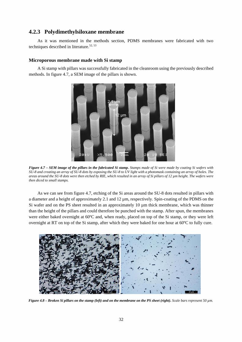
32
4.2.3 Polydimethylsiloxane membrane
As it was mentioned in the methods section, PDMS membranes were fabricated with two
techniques described in literature.52, 53
Microporous membrane made with Si stamp
A Si stamp with pillars was successfully fabricated in the cleanroom using the previously described
methods. In figure 4.7, a SEM image of the pillars is shown.
As we can see from figure 4.7, etching of the Si areas around the SU-8 dots resulted in pillars with
a diameter and a height of approximately 2.1 and 12 µm, respectively. Spin-coating of the PDMS on the
Si wafer and on the PS sheet resulted in an approximately 10 µm thick membrane, which was thinner
than the height of the pillars and could therefore be punched with the stamp. After spun, the membranes
were either baked overnight at 60ºC and, when ready, placed on top of the Si stamp, or they were left
overnight at RT on top of the Si stamp, after which they were baked for one hour at 60ºC to fully cure.
Figure 4.7 – SEM image of the pillars in the fabricated Si stamp. Stamps made of Si were made by coating Si wafers with
SU-8 and creating an array of SU-8 dots by exposing the SU-8 to UV light with a photomask containing an array of holes. The
areas around the SU-8 dots were then etched by RIE, which resulted in an array of Si pillars of 12 µm height. The wafers were
then diced to small stamps.
Figure 4.8 – Broken Si pillars on the stamp (left) and on the membrane on the PS sheet (right). Scale bars represent 50 µm.
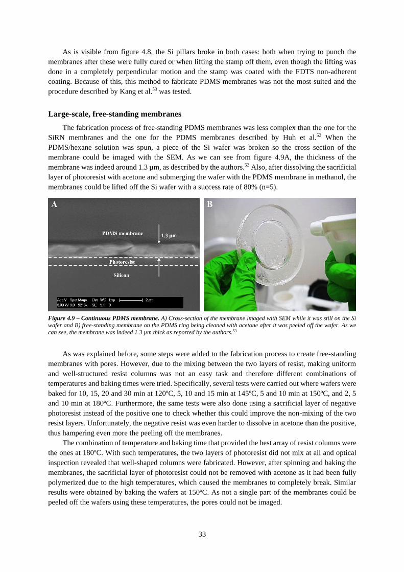
33
As is visible from figure 4.8, the Si pillars broke in both cases: both when trying to punch the
membranes after these were fully cured or when lifting the stamp off them, even though the lifting was
done in a completely perpendicular motion and the stamp was coated with the FDTS non-adherent
coating. Because of this, this method to fabricate PDMS membranes was not the most suited and the
procedure described by Kang et al.53 was tested.
Large-scale, free-standing membranes
The fabrication process of free-standing PDMS membranes was less complex than the one for the
SiRN membranes and the one for the PDMS membranes described by Huh et al.52 When the
PDMS/hexane solution was spun, a piece of the Si wafer was broken so the cross section of the
membrane could be imaged with the SEM. As we can see from figure 4.9A, the thickness of the
membrane was indeed around 1.3 µm, as described by the authors.53 Also, after dissolving the sacrificial
layer of photoresist with acetone and submerging the wafer with the PDMS membrane in methanol, the
membranes could be lifted off the Si wafer with a success rate of 80% (n=5).
As was explained before, some steps were added to the fabrication process to create free-standing
membranes with pores. However, due to the mixing between the two layers of resist, making uniform
and well-structured resist columns was not an easy task and therefore different combinations of
temperatures and baking times were tried. Specifically, several tests were carried out where wafers were
baked for 10, 15, 20 and 30 min at 120ºC, 5, 10 and 15 min at 145ºC, 5 and 10 min at 150ºC, and 2, 5
and 10 min at 180ºC. Furthermore, the same tests were also done using a sacrificial layer of negative
photoresist instead of the positive one to check whether this could improve the non-mixing of the two
resist layers. Unfortunately, the negative resist was even harder to dissolve in acetone than the positive,
thus hampering even more the peeling off the membranes.
The combination of temperature and baking time that provided the best array of resist columns were
the ones at 180ºC. With such temperatures, the two layers of photoresist did not mix at all and optical
inspection revealed that well-shaped columns were fabricated. However, after spinning and baking the
membranes, the sacrificial layer of photoresist could not be removed with acetone as it had been fully
polymerized due to the high temperatures, which caused the membranes to completely break. Similar
results were obtained by baking the wafers at 150ºC. As not a single part of the membranes could be
peeled off the wafers using these temperatures, the pores could not be imaged.
Figure 4.9 – Continuous PDMS membrane. A) Cross-section of the membrane imaged with SEM while it was still on the Si
wafer and B) free-standing membrane on the PDMS ring being cleaned with acetone after it was peeled off the wafer. As we
can see, the membrane was indeed 1.3 µm thick as reported by the authors.53
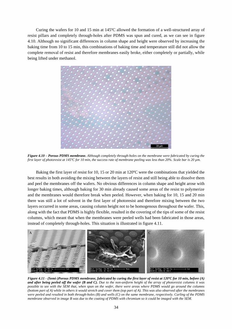
34
Curing the wafers for 10 and 15 min at 145ºC allowed the formation of a well-structured array of
resist pillars and completely through-holes after PDMS was spun and cured, as we can see in figure
4.10. Although no significant differences in column shape and height were observed by increasing the
baking time from 10 to 15 min, this combinations of baking time and temperature still did not allow the
complete removal of resist and therefore membranes easily broke, either completely or partially, while
being lifted under methanol.
Baking the first layer of resist for 10, 15 or 20 min at 120ºC were the combinations that yielded the
best results in both avoiding the mixing between the layers of resist and still being able to dissolve them
and peel the membranes off the wafers. No obvious differences in column shape and height arose with
longer baking times, although baking for 30 min already caused some areas of the resist to polymerize
and the membranes would therefore break when peeled. However, when baking for 10, 15 and 20 min
there was still a lot of solvent in the first layer of photoresist and therefore mixing between the two
layers occurred in some areas, causing column height not to be homogenous throughout the wafer. This,
along with the fact that PDMS is highly flexible, resulted in the covering of the tips of some of the resist
columns, which meant that when the membranes were peeled wells had been fabricated in those areas,
instead of completely through-holes. This situation is illustrated in figure 4.11.
Figure 4.10 – Porous PDMS membrane. Although completely through-holes on the membrane were fabricated by curing the
first layer of photoresist at 145ºC for 10 min, the success rate of membrane peeling was less than 20%. Scale bar is 20 µm.
Figure 4.11 - (Semi-)Porous PDMS membrane, fabricated by curing the first layer of resist at 120ºC for 10 min, before (A)
and after being peeled off the wafer (B and C). Due to the non-uniform height of the array of photoresist columns it was
possible to see with the SEM that, when spun on the wafer, there were areas where PDMS would go around the columns
(bottom part of A) while in others it would stretch and cover them (top part of A). This was also observed after the membranes
were peeled and resulted in both through-holes (B) and wells (C) on the same membrane, respectively. Curling of the PDMS
membrane observed in image B was due to the coating of PDMS with chromium so it could be imaged with the SEM.
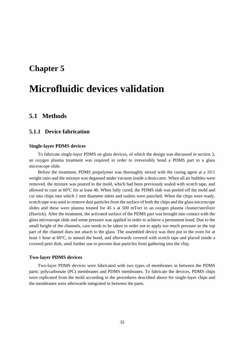
35
Chapter 5
Microfluidic devices validation
5.1 Methods
5.1.1 Device fabrication
Single-layer PDMS devices
To fabricate single-layer PDMS on glass devices, of which the design was discussed in section 3,
an oxygen plasma treatment was required in order to irreversibly bond a PDMS part to a glass
microscope slide.
Before the treatment, PDMS prepolymer was thoroughly mixed with the curing agent at a 10:1
weight ratio and the mixture was degassed under vacuum inside a desiccator. When all air bubbles were
removed, the mixture was poured in the mold, which had been previously sealed with scotch tape, and
allowed to cure at 60ºC for at least 4h. When fully cured, the PDMS slab was peeled off the mold and
cut into chips into which 1 mm diameter inlets and outlets were punched. When the chips were ready,
scotch tape was used to remove dust particles from the surface of both the chips and the glass microscope
slides and these were plasma treated for 45 s at 500 mTorr in an oxygen plasma cleaner/sterilizer
(Harrick). After the treatment, the activated surface of the PDMS part was brought into contact with the
glass microscope slide and some pressure was applied in order to achieve a permanent bond. Due to the
small height of the channels, care needs to be taken in order not to apply too much pressure so the top
part of the channel does not attach to the glass. The assembled device was then put in the oven for at
least 1 hour at 60ºC, to anneal the bond, and afterwards covered with scotch tape and placed inside a
covered petri dish, until further use to prevent dust particles from gathering into the chip.
Two-layer PDMS devices
Two-layer PDMS devices were fabricated with two types of membranes in between the PDMS
parts: polycarbonate (PC) membranes and PDMS membranes. To fabricate the devices, PDMS chips
were replicated from the mold according to the procedures described above for single-layer chips and
the membranes were afterwards integrated in between the parts.
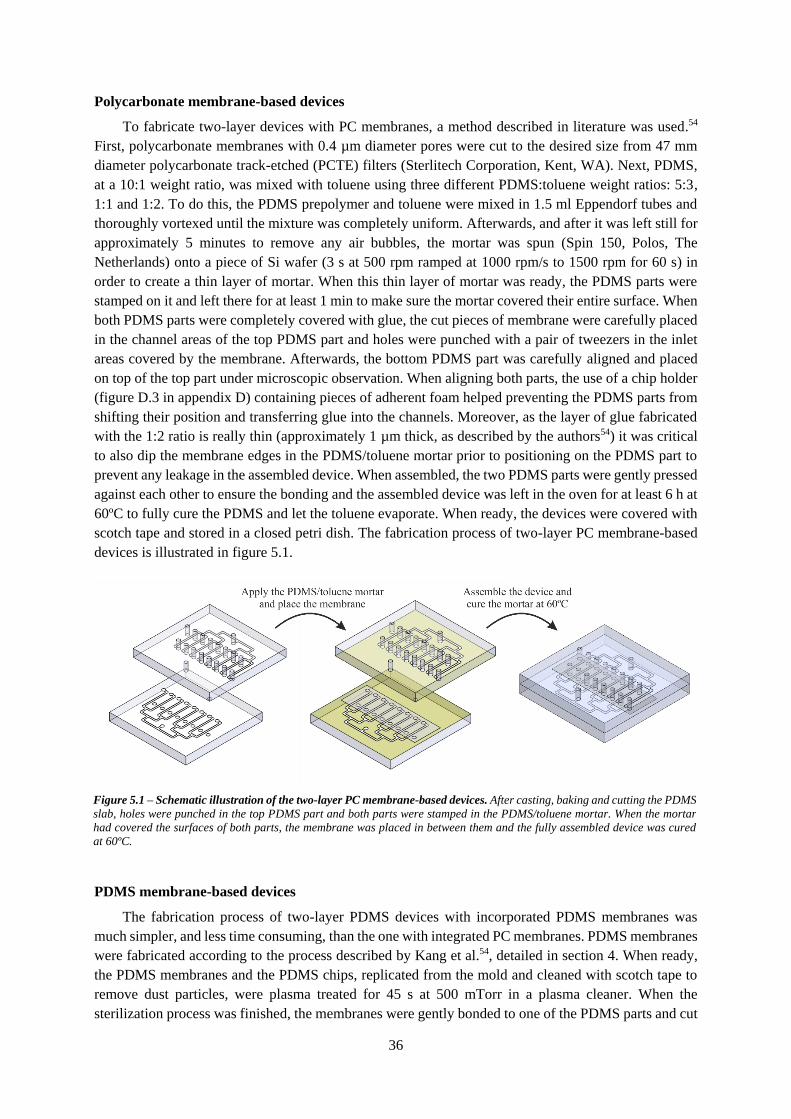
36
Polycarbonate membrane-based devices
To fabricate two-layer devices with PC membranes, a method described in literature was used.54
First, polycarbonate membranes with 0.4 µm diameter pores were cut to the desired size from 47 mm
diameter polycarbonate track-etched (PCTE) filters (Sterlitech Corporation, Kent, WA). Next, PDMS,
at a 10:1 weight ratio, was mixed with toluene using three different PDMS:toluene weight ratios: 5:3,
1:1 and 1:2. To do this, the PDMS prepolymer and toluene were mixed in 1.5 ml Eppendorf tubes and
thoroughly vortexed until the mixture was completely uniform. Afterwards, and after it was left still for
approximately 5 minutes to remove any air bubbles, the mortar was spun (Spin 150, Polos, The
Netherlands) onto a piece of Si wafer (3 s at 500 rpm ramped at 1000 rpm/s to 1500 rpm for 60 s) in
order to create a thin layer of mortar. When this thin layer of mortar was ready, the PDMS parts were
stamped on it and left there for at least 1 min to make sure the mortar covered their entire surface. When
both PDMS parts were completely covered with glue, the cut pieces of membrane were carefully placed
in the channel areas of the top PDMS part and holes were punched with a pair of tweezers in the inlet
areas covered by the membrane. Afterwards, the bottom PDMS part was carefully aligned and placed
on top of the top part under microscopic observation. When aligning both parts, the use of a chip holder
(figure D.3 in appendix D) containing pieces of adherent foam helped preventing the PDMS parts from
shifting their position and transferring glue into the channels. Moreover, as the layer of glue fabricated
with the 1:2 ratio is really thin (approximately 1 µm thick, as described by the authors54) it was critical
to also dip the membrane edges in the PDMS/toluene mortar prior to positioning on the PDMS part to
prevent any leakage in the assembled device. When assembled, the two PDMS parts were gently pressed
against each other to ensure the bonding and the assembled device was left in the oven for at least 6 h at
60ºC to fully cure the PDMS and let the toluene evaporate. When ready, the devices were covered with
scotch tape and stored in a closed petri dish. The fabrication process of two-layer PC membrane-based
devices is illustrated in figure 5.1.
PDMS membrane-based devices
The fabrication process of two-layer PDMS devices with incorporated PDMS membranes was
much simpler, and less time consuming, than the one with integrated PC membranes. PDMS membranes
were fabricated according to the process described by Kang et al.54, detailed in section 4. When ready,
the PDMS membranes and the PDMS chips, replicated from the mold and cleaned with scotch tape to
remove dust particles, were plasma treated for 45 s at 500 mTorr in a plasma cleaner. When the
sterilization process was finished, the membranes were gently bonded to one of the PDMS parts and cut
Figure 5.1 – Schematic illustration of the two-layer PC membrane-based devices. After casting, baking and cutting the PDMS
slab, holes were punched in the top PDMS part and both parts were stamped in the PDMS/toluene mortar. When the mortar
had covered the surfaces of both parts, the membrane was placed in between them and the fully assembled device was cured
at 60ºC.
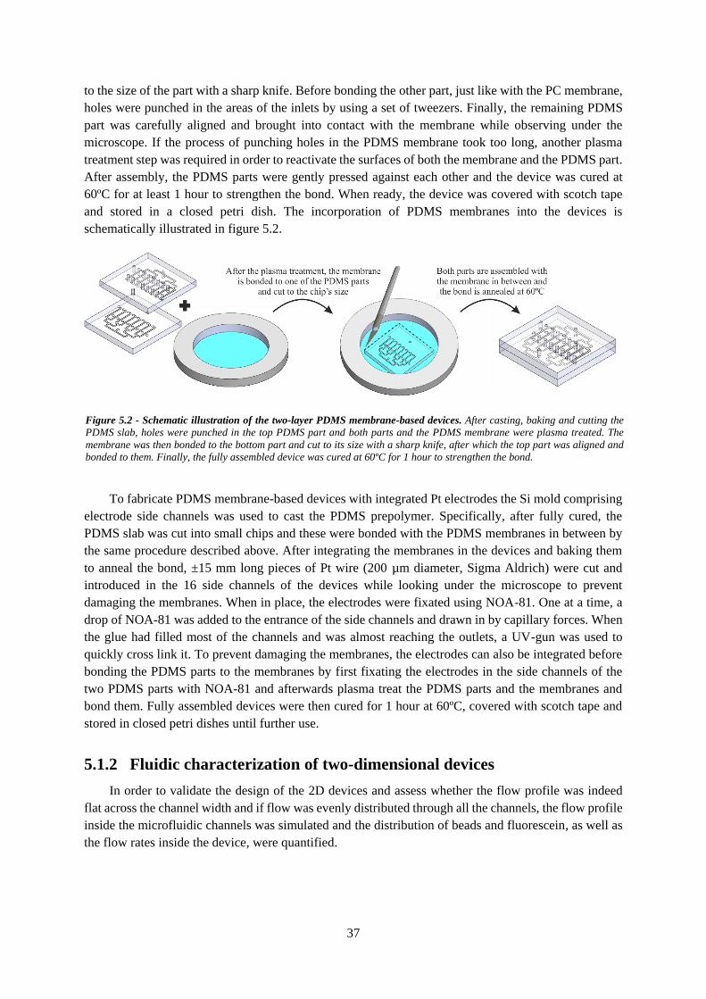
37
to the size of the part with a sharp knife. Before bonding the other part, just like with the PC membrane,
holes were punched in the areas of the inlets by using a set of tweezers. Finally, the remaining PDMS
part was carefully aligned and brought into contact with the membrane while observing under the
microscope. If the process of punching holes in the PDMS membrane took too long, another plasma
treatment step was required in order to reactivate the surfaces of both the membrane and the PDMS part.
After assembly, the PDMS parts were gently pressed against each other and the device was cured at
60ºC for at least 1 hour to strengthen the bond. When ready, the device was covered with scotch tape
and stored in a closed petri dish. The incorporation of PDMS membranes into the devices is
schematically illustrated in figure 5.2.
To fabricate PDMS membrane-based devices with integrated Pt electrodes the Si mold comprising
electrode side channels was used to cast the PDMS prepolymer. Specifically, after fully cured, the
PDMS slab was cut into small chips and these were bonded with the PDMS membranes in between by
the same procedure described above. After integrating the membranes in the devices and baking them
to anneal the bond, ±15 mm long pieces of Pt wire (200 µm diameter, Sigma Aldrich) were cut and
introduced in the 16 side channels of the devices while looking under the microscope to prevent
damaging the membranes. When in place, the electrodes were fixated using NOA-81. One at a time, a
drop of NOA-81 was added to the entrance of the side channels and drawn in by capillary forces. When
the glue had filled most of the channels and was almost reaching the outlets, a UV-gun was used to
quickly cross link it. To prevent damaging the membranes, the electrodes can also be integrated before
bonding the PDMS parts to the membranes by first fixating the electrodes in the side channels of the
two PDMS parts with NOA-81 and afterwards plasma treat the PDMS parts and the membranes and
bond them. Fully assembled devices were then cured for 1 hour at 60ºC, covered with scotch tape and
stored in closed petri dishes until further use.
5.1.2 Fluidic characterization of two-dimensional devices
In order to validate the design of the 2D devices and assess whether the flow profile was indeed
flat across the channel width and if flow was evenly distributed through all the channels, the flow profile
inside the microfluidic channels was simulated and the distribution of beads and fluorescein, as well as
the flow rates inside the device, were quantified.
Figure 5.2 - Schematic illustration of the two-layer PDMS membrane-based devices. After casting, baking and cutting the
PDMS slab, holes were punched in the top PDMS part and both parts and the PDMS membrane were plasma treated. The
membrane was then bonded to the bottom part and cut to its size with a sharp knife, after which the top part was aligned and
bonded to them. Finally, the fully assembled device was cured at 60ºC for 1 hour to strengthen the bond.
38
Beads and fluorescein distribution
To mimic the introduction of cells and culture media inside the 2D device, beads and fluorescein
were introduced through the common inlets of the chips with a single pipetting action.
A suspension of 10 µm polystyrene beads was prepared by adding 2 drops of beads to 5 ml of
culture media, resulting in approximately 7.6 × 10⁵ beads/ml. After thorough vortexing, 35 µl of the
suspension was pipetted and pictures were taken of all the channels. In order to analyze the distribution
of beads, these were counted in every picture (channel) using ImageJ software and the results were
compared. Something similar was done with fluorescein, where also 35 µl of solution was pipetted into
the devices and pictures were taken to every channel. The results were then analyzed by measuring the
intensity of fluorescein in every picture (channel), also with ImageJ software.
Flow inside the channels
Flow rates inside the 2D microfluidic device were assessed both theoretically and experimentally.
As it was explained before, one of the main advantages when culturing cells in an organ-on-chip
platform is that it allows the continuous perfusion of the microfluidic channels and therefore seeded
cells can be exposed to physiologically relevant shear stress. In case of the human brain, such shear is
known to be between 0.3 and 2 Pa.36, 55 For this reason, we decided to investigate what flow rate could
induce a shear stress of 0.5 Pa in the channels of our platform.
If we consider, and rearrange, equation 2.1, the required volumetric flow rate to achieve such shear
inside each of the channels is estimated at approximately 9 µl/min:
𝑄 =𝜏 · 𝑤 · ℎ2
6 · µ · (1 +ℎ𝑤
) · 𝑓 · (ℎ𝑤
)
𝑄 =0.5 𝑃𝑎 · 0.5 · 0.052
6 · 0.7 · 10−3 · (1 +0.050.5
) · 0.8820= 0.1534 𝑚𝑚3/𝑠 ≈ 0.15 µ𝑙/𝑠 = 9 µ𝑙/𝑚𝑖𝑛
However, one must take into account that as the chip has 8 channels and, in principle, the flow is
evenly split, a flow rate of 72 µl/min at the inlet is needed if we want to reproduce a shear stress of 0.5
Pa in each of the parallel microfluidic channels when dynamically culturing cells.
In this way, a simulation in COMSOL Multiphysics 5.0 software (COMSOL®) was done to assess
whether the geometry of our device worked theoretically. Moreover, to experimentally verify if the flow
indeed split evenly and the flow rates were similar in all the channels and relevant shear stress could be
replicated, an experiment to calculate the flow rates inside each channel of the device was also carried
out.
Simulation
Flow rates inside the device were simulated using COMSOL Multiphysics 5.0 software. To do it,
the geometry of the device was built and all the parameters defined. Specifically, a laminar and
stationary flow study was chosen. The fluid inside the model was chosen to be water in order to resemble
the culture medium and the flow was set as incompressible and no turbulence was introduced to the
model. The boundary conditions were the inlet, with a laminar inflow flow rate of 72 µl/min and an
entrance length and thickness of 500 µm and 50 µm, respectively, the eight outlets, all at atmospheric
pressure (0 Pa), and the walls, with a “no slip” boundary condition. The mesh was generated by a free
triangular generator and element size was defined as extremely fine. Furthermore, the averaged flow
(5.1)
39
rates were calculated from the average velocities obtained for each channel and a cut line was done
along the channel’s width to verify what the velocity magnitude in each channel was.
Experiment
To experimentally validate the simulation that was done in COMSOL, the flow rates inside each
channel of the device were measured. To do that, the same beads suspension used to evaluate the beads
distribution throughout the device was pumped at a flow rate of 72 µl/min at the inlet. This was achieved
with a Nemesys syringe pump (CETONI GmbH), equipped with a 3 ml BD syringe (Becton, Dickinson
and Company, Franklin Lakes, NJ), with Tygon tubing (inner diameter (ID) 1.27 mm, outer diameter
(OD) 2.29 mm; Saint-Gobain performance plastics group) and metal syringe tips. To minimize the
hydrostatic pressure differences at the outlets, the top surface of the chip was completely covered with
EGM-2 culture medium. Movies of the beads flowing were recorded for every channel with a high speed
camera (Phantom), from which the velocities of the beads (and consequently, the flow rates) inside the
channels were determined using three different MATLAB (MathWorks) scripts (the first developed by
MathWorks Inc. and the remaining two by Bjorn de Wagenaar and Stefan Dekker, former and current
BIOS Lab on a Chip group members, respectively).
5.1.3 Characterization of lumen robustness in the 3D devices
After the fabrication process of the 3D BBB multiplex devices was optimized, it was time to assess
whether the obtained model could allow the creation of hollow lumens in the collagen gel and if these
lumens were robust enough to allow the culturing of the endothelial cells in their inner surfaces. To
create the collagen I lumens inside the chambers of the device, 9.15 mg/ml collagen I (Corning Life
Sciences) was diluted to a final concentration of 6.5 mg/ml according to the manufacturer’s
specifications (10% phosphate-buffered saline (PBS, Sigma-Aldrich), 71% Collagen I, 1,6% sodium
hydroxide (NaOH) and 17,4% deionized (DI) water). When ready, collagen was introduced in the
chambers of the devices and 800 µm diameter microneedles were inserted through the holes of the caps.
After placing the needles, collagen was set by incubating the devices at 37ºC, for 1 hour. The hollow
collagen I channels were then created by slowly pulling the micro needles out of the devices. With this,
the fabrication process of the 3D chips was concluded and cells could now be cultured in the lumens.
To determine the robustness of the lumens created within collagen I, experiments with beads were
performed. This was done by pipetting 15 µl of beads suspension into each lumen and afterwards
imaging the channels and the collagen surrounding them to determine whether the beads had stayed
inside the lumens or crossed their walls.
5.1.4 On-chip cell culture
Human cerebral microvascular endothelial cell line
Immortalized human cerebral microvascular endothelial cells (hCMEC/D3) were the chosen cell
line to use in the BBB multiplex chip. The cell line was derived from human temporal lobe microvessels
isolated from tissue excised during surgery for control of epilepsy in an adult female. The obtained
endothelial cells were sequentially immortalized by lentiviral vector transduction of the telomerase
complex and proto-oncogenes.28 Some of the factors that made us choose this cell line were their human
origin, low variability, ease of culturing and the fact that they maintain their phenotype until at least
passage 35.31, 56
40
For the purpose of the present work, vials containing hCMEC cells suspended in complete medium
in the presence of the cryo-protective agent dimethylsulfoxide (DMSO) were thawed from a tank filled
with liquid nitrogen. When thawed, the vials were warmed up for approximately 2-3 minutes and the
cell suspensions were pipetted into collagen I-coated T75 flasks (Greiner Bio-One) that had been
previously filled with endothelial growth medium-2 (EGM-2, Lonza), which consists of endothelial
basic medium-2 (EBM-2, Lonza) supplemented with an EGM-2 BulletKit (Lonza), and the flasks were
incubated at 37ºC and 5% CO2 humidified air. In order to separate the cell pellet from the DMSO and
thus prevent cell damage, a centrifuge step at 390 rpm for 5 min can also be done before plating the cells
in the collagen I-coated T75 flasks. When cell confluence was around 90% the cells were passed by first
washing with PBS and subsequently incubating 0.05% trypsin (Gibco) in the flasks for 5 min at 37ºC to
promote cell detachment from the flasks. After this, the cell suspension was collected and centrifuged
for 5 min. at 390 rpm and the pellet was resuspended in EGM-2 and replated at 1:3 or 1:4 into new
collagen I-coated flasks, already containing EGM-2, or seeded in microfluidic devices. Cells were
passed every 2 days and in all the reported experiments hCMEC/D3 cells between passages 28 and 33
were used.
Single-layer and two-layer 2D BBB multiplex devices
Cell culturing in both 1 and 2 layer PDMS devices followed the same protocol. Prior to culturing
the cells, a plasma treatment was done to the devices in order to make PDMS hydrophilic and thus
minimize the chance of having air trapped inside the device. After the plasma treatment, the devices
were flushed with PBS and coated with 35 µl of 40 µg/ml fibronectin (FN, Gibco) in PBS for 2 hours at
37ºC. After 2 hours, the devices were rinsed with culture medium and left at room temperature (RT)
until the cells were ready to be seeded. hCMEC/D3 cells from a confluent T75 culture flask were counted
using a Luna cell counter (Logos Biosystems) and resuspended in EGM-2 to reach a concentration of
40×106 cells/ml. 35 µl of the cell suspension were then loaded into the 8 channels of the devices with a
single pipetting action and the top part of the devices was covered with medium to prevent flow due to
hydrostatic pressure differences between the outlets. Cells were allowed to attach for at least 1 hour
inside the incubator, after which the devices were flushed with fresh EGM-2 medium to wash away the
unattached cells. Medium was refreshed two times per day by inserting pipette tips with 200 µl of new
EGM-2 medium in the inlets of the devices.
3D BBB multiplex devices
Cell culturing in the 3D devices started after the collagen lumens had been created. When ready,
the inner surfaces of the hollow lumens were coated with 40 µg/ml FN, to promote cell adhesion to the
collagen, and incubated for at least 2 hours. Afterwards, culture medium was flushed through the lumens
to wash away the FN and the devices were left at room temperature until the cells were ready to be
seeded. After counting and resuspending the hCMEC/D3 cells to a concentration of 20×106 cells/ml, 15
µl of the cell suspension was introduced in all the lumens and the devices were placed in the incubator.
The devices were flipped upside-down 10 min later to allow cell adhesion on the opposite side of the
lumens and, approximately 1 hour later, sunk in a small petri dish filled with 5 ml of EGM-2 culture
medium, which was refreshed every 24 hours.
41
5.1.5 Cell observation
Cells in culture flasks and microfluidic devices were monitored and imaged with Leica DMI5000
M (camera was operated by Leica Application Suite 4.2.0) and EVOS FL (Life Technologies)
microscopes. In the culture flaks, imaging of the cells was only done with phase contrast, whereas cells
in the devices were imaged both with phase contrast and fluorescence microscopy. Cells seeded on the
PC membrane areas of the membrane-based devices, however, could only be imaged with fluorescence
microscopy due to the opacity of the PC membrane. Moreover, live/dead stainings were also done to
assess the viability of the hCMEC/D3 cells both on the PC membrane and after individually addressing
the channels of the 2D devices.
Fluorescent staining
After 5 days of culture, cells in the microfluidic devices were stained for the nuclei and F-actin.
Prior to applying the staining, cells were rinsed with PBS and fixated with 3.7% paraformaldehyde
(Sigma Aldrich) in PBS. After an incubation period of 30 minutes at RT, the fixative was thoroughly
washed away with PBS and the staining procedure took place. To stain the cells, the cell membranes
were permeabilized by adding a permeabilization buffer (PB) consisting of 0.1% (v/v) Triton X-100 and
1% (m/m) bovine serum albumin (BSA, Sigma) in PBS and incubating the devices for 15 min at RT.
Then, a staining solution containing 42 µl of NucBlue (Ready Probes reagent, Molecular Probes, Life
Technologies) and 12.5 µl of actin green (Molecular probes, Life Technologies) in PB was flushed
through the devices and these were incubated for at least 30 min, in the dark, at RT. After the incubation
period, the devices were flushed at least two times with PBS and then stored in a closed, humidified
petri dish, when not imaged right after. The actin filaments of the cells inside the one-layer PDMS
devices were stained with phalloidin labeled with Texas Red (Molecular Probes, Life Technologies)
instead of actin green. The channel of the acquired images was then switched from red to green, with
ImageJ software, to enhance contrast.
Live/dead staining
To assess the viability of the hCMEC/D3 cells on the PC membrane, cells were cultured for 5 days
and a live/dead staining solution consisting of 1 µl of calcein-AM and 4 µl of ethidium homodimer-1
(LIVE/DEAD® Viability/Cytotoxicity Kit for mammalian cells, Invitrogen), 42 µl of NucBlue and 60
µl of PBS was inserted in the devices after flushing them at least 2 or 3 times with PBS. The devices
were then incubated for 30 min at 37ºC, after which they were imaged. When the channels of the 2D
devices were individually addressed, live/dead stainings equal to the ones described above were done to
determine the viability of the hCMEC/D3 cell layers after the experiments.
5.1.6 Mechanical modulation
The influence that mechanically modulating the hCMEC/D3 cell layer could have on cell growth
and morphology was studied by exposing the cells inside the microfluidic channels of the 2D devices to
a shear stress of 0.5 Pa, after 24 hours of static culture. To do this, EGM-2 culture medium was pumped
by a Harvard PHD 2000 programmable syringe pump through the inlets of the microfluidic devices at a
flow rate of 72 µl/min (approximately 9 µl/min inside each channel). The pump was equipped with a 50
ml BD Plastipak luer-lock syringe, which was connected to a bubble trap by Tygon tubing (ID 1.27 mm,
OD 2.29 mm) and a needle. The bubble trap consisted of a glass vial half-full with culture medium and
sealed with an air-tight septum to prevent air from entering the devices and was connected to the devices
by a needle, Tygon tubing and a metal syringe tip, which had been previously coated with 10 mg/ml
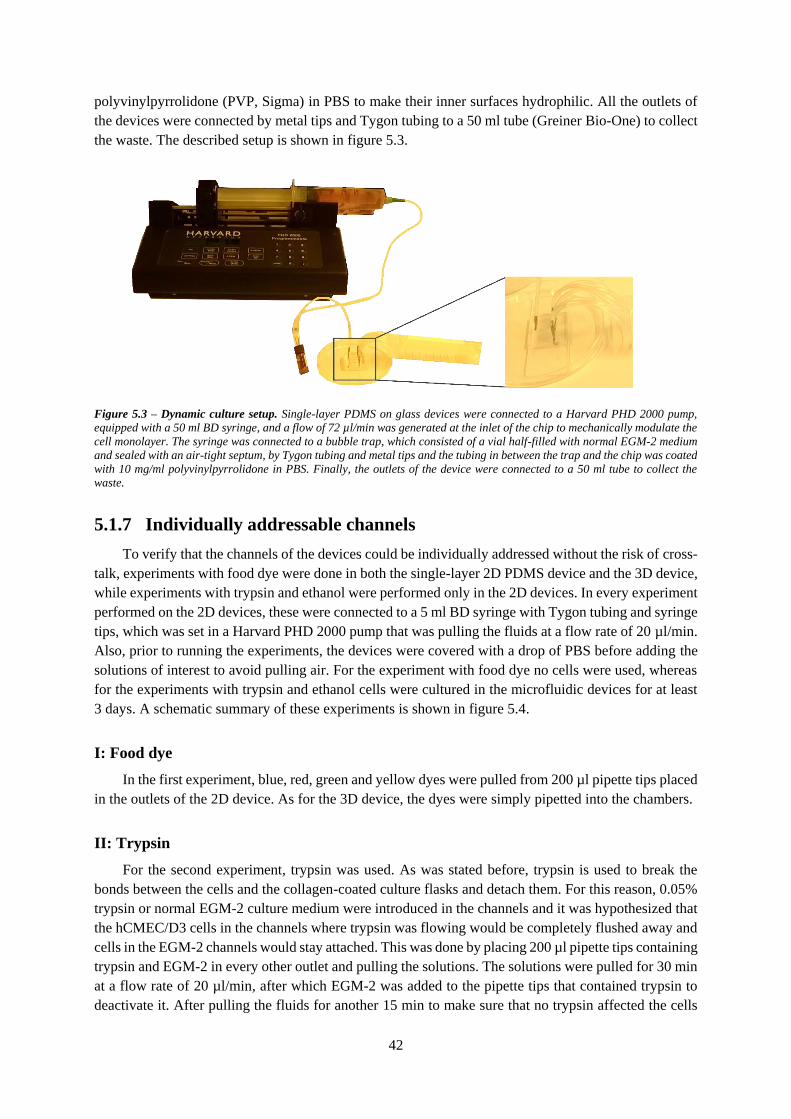
42
polyvinylpyrrolidone (PVP, Sigma) in PBS to make their inner surfaces hydrophilic. All the outlets of
the devices were connected by metal tips and Tygon tubing to a 50 ml tube (Greiner Bio-One) to collect
the waste. The described setup is shown in figure 5.3.
5.1.7 Individually addressable channels
To verify that the channels of the devices could be individually addressed without the risk of cross-
talk, experiments with food dye were done in both the single-layer 2D PDMS device and the 3D device,
while experiments with trypsin and ethanol were performed only in the 2D devices. In every experiment
performed on the 2D devices, these were connected to a 5 ml BD syringe with Tygon tubing and syringe
tips, which was set in a Harvard PHD 2000 pump that was pulling the fluids at a flow rate of 20 µl/min.
Also, prior to running the experiments, the devices were covered with a drop of PBS before adding the
solutions of interest to avoid pulling air. For the experiment with food dye no cells were used, whereas
for the experiments with trypsin and ethanol cells were cultured in the microfluidic devices for at least
3 days. A schematic summary of these experiments is shown in figure 5.4.
I: Food dye
In the first experiment, blue, red, green and yellow dyes were pulled from 200 µl pipette tips placed
in the outlets of the 2D device. As for the 3D device, the dyes were simply pipetted into the chambers.
II: Trypsin
For the second experiment, trypsin was used. As was stated before, trypsin is used to break the
bonds between the cells and the collagen-coated culture flasks and detach them. For this reason, 0.05%
trypsin or normal EGM-2 culture medium were introduced in the channels and it was hypothesized that
the hCMEC/D3 cells in the channels where trypsin was flowing would be completely flushed away and
cells in the EGM-2 channels would stay attached. This was done by placing 200 µl pipette tips containing
trypsin and EGM-2 in every other outlet and pulling the solutions. The solutions were pulled for 30 min
at a flow rate of 20 µl/min, after which EGM-2 was added to the pipette tips that contained trypsin to
deactivate it. After pulling the fluids for another 15 min to make sure that no trypsin affected the cells
Figure 5.3 – Dynamic culture setup. Single-layer PDMS on glass devices were connected to a Harvard PHD 2000 pump,
equipped with a 50 ml BD syringe, and a flow of 72 µl/min was generated at the inlet of the chip to mechanically modulate the
cell monolayer. The syringe was connected to a bubble trap, which consisted of a vial half-filled with normal EGM-2 medium
and sealed with an air-tight septum, by Tygon tubing and metal tips and the tubing in between the trap and the chip was coated
with 10 mg/ml polyvinylpyrrolidone in PBS. Finally, the outlets of the device were connected to a 50 ml tube to collect the
waste.
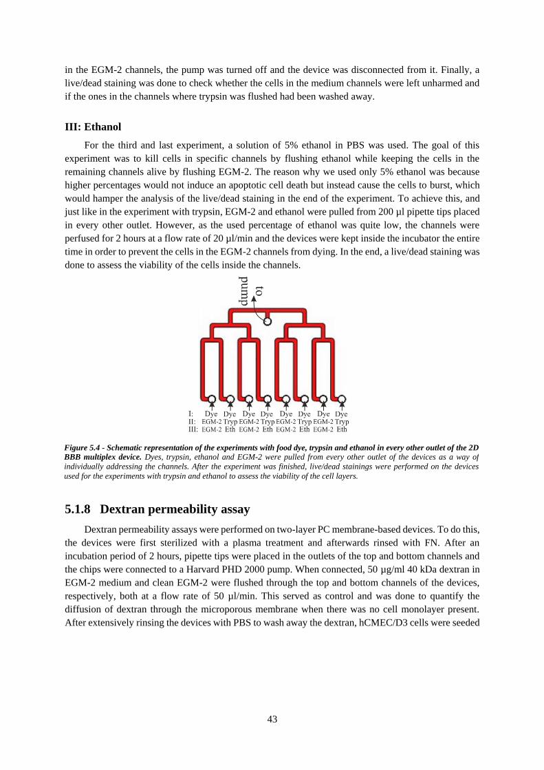
43
in the EGM-2 channels, the pump was turned off and the device was disconnected from it. Finally, a
live/dead staining was done to check whether the cells in the medium channels were left unharmed and
if the ones in the channels where trypsin was flushed had been washed away.
III: Ethanol
For the third and last experiment, a solution of 5% ethanol in PBS was used. The goal of this
experiment was to kill cells in specific channels by flushing ethanol while keeping the cells in the
remaining channels alive by flushing EGM-2. The reason why we used only 5% ethanol was because
higher percentages would not induce an apoptotic cell death but instead cause the cells to burst, which
would hamper the analysis of the live/dead staining in the end of the experiment. To achieve this, and
just like in the experiment with trypsin, EGM-2 and ethanol were pulled from 200 µl pipette tips placed
in every other outlet. However, as the used percentage of ethanol was quite low, the channels were
perfused for 2 hours at a flow rate of 20 µl/min and the devices were kept inside the incubator the entire
time in order to prevent the cells in the EGM-2 channels from dying. In the end, a live/dead staining was
done to assess the viability of the cells inside the channels.
5.1.8 Dextran permeability assay
Dextran permeability assays were performed on two-layer PC membrane-based devices. To do this,
the devices were first sterilized with a plasma treatment and afterwards rinsed with FN. After an
incubation period of 2 hours, pipette tips were placed in the outlets of the top and bottom channels and
the chips were connected to a Harvard PHD 2000 pump. When connected, 50 µg/ml 40 kDa dextran in
EGM-2 medium and clean EGM-2 were flushed through the top and bottom channels of the devices,
respectively, both at a flow rate of 50 µl/min. This served as control and was done to quantify the
diffusion of dextran through the microporous membrane when there was no cell monolayer present.
After extensively rinsing the devices with PBS to wash away the dextran, hCMEC/D3 cells were seeded
Figure 5.4 - Schematic representation of the experiments with food dye, trypsin and ethanol in every other outlet of the 2D
BBB multiplex device. Dyes, trypsin, ethanol and EGM-2 were pulled from every other outlet of the devices as a way of
individually addressing the channels. After the experiment was finished, live/dead stainings were performed on the devices
used for the experiments with trypsin and ethanol to assess the viability of the cell layers.
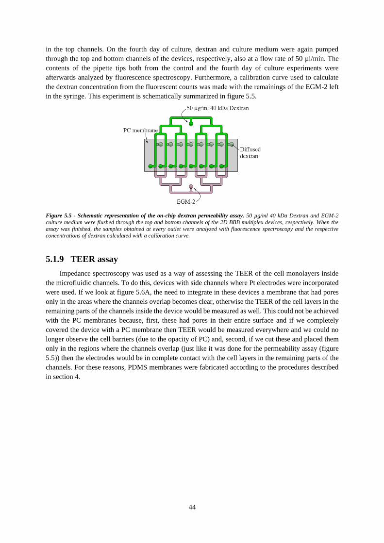
44
in the top channels. On the fourth day of culture, dextran and culture medium were again pumped
through the top and bottom channels of the devices, respectively, also at a flow rate of 50 µl/min. The
contents of the pipette tips both from the control and the fourth day of culture experiments were
afterwards analyzed by fluorescence spectroscopy. Furthermore, a calibration curve used to calculate
the dextran concentration from the fluorescent counts was made with the remainings of the EGM-2 left
in the syringe. This experiment is schematically summarized in figure 5.5.
5.1.9 TEER assay
Impedance spectroscopy was used as a way of assessing the TEER of the cell monolayers inside
the microfluidic channels. To do this, devices with side channels where Pt electrodes were incorporated
were used. If we look at figure 5.6A, the need to integrate in these devices a membrane that had pores
only in the areas where the channels overlap becomes clear, otherwise the TEER of the cell layers in the
remaining parts of the channels inside the device would be measured as well. This could not be achieved
with the PC membranes because, first, these had pores in their entire surface and if we completely
covered the device with a PC membrane then TEER would be measured everywhere and we could no
longer observe the cell barriers (due to the opacity of PC) and, second, if we cut these and placed them
only in the regions where the channels overlap (just like it was done for the permeability assay (figure
5.5)) then the electrodes would be in complete contact with the cell layers in the remaining parts of the
channels. For these reasons, PDMS membranes were fabricated according to the procedures described
in section 4.
Figure 5.5 - Schematic representation of the on-chip dextran permeability assay. 50 µg/ml 40 kDa Dextran and EGM-2
culture medium were flushed through the top and bottom channels of the 2D BBB multiplex devices, respectively. When the
assay was finished, the samples obtained at every outlet were analyzed with fluorescence spectroscopy and the respective
concentrations of dextran calculated with a calibration curve.
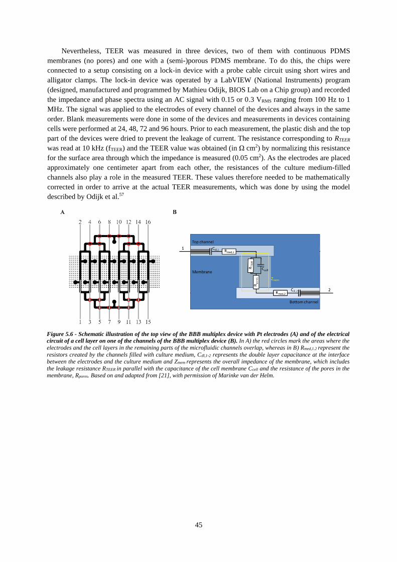
45
Nevertheless, TEER was measured in three devices, two of them with continuous PDMS
membranes (no pores) and one with a (semi-)porous PDMS membrane. To do this, the chips were
connected to a setup consisting on a lock-in device with a probe cable circuit using short wires and
alligator clamps. The lock-in device was operated by a LabVIEW (National Instruments) program
(designed, manufactured and programmed by Mathieu Odijk, BIOS Lab on a Chip group) and recorded
the impedance and phase spectra using an AC signal with 0.15 or 0.3 VRMS ranging from 100 Hz to 1
MHz. The signal was applied to the electrodes of every channel of the devices and always in the same
order. Blank measurements were done in some of the devices and measurements in devices containing
cells were performed at 24, 48, 72 and 96 hours. Prior to each measurement, the plastic dish and the top
part of the devices were dried to prevent the leakage of current. The resistance corresponding to RTEER
was read at 10 kHz (fTEER) and the TEER value was obtained (in Ω cm2) by normalizing this resistance
for the surface area through which the impedance is measured (0.05 cm2). As the electrodes are placed
approximately one centimeter apart from each other, the resistances of the culture medium-filled
channels also play a role in the measured TEER. These values therefore needed to be mathematically
corrected in order to arrive at the actual TEER measurements, which was done by using the model
described by Odijk et al.57
Figure 5.6 - Schematic illustration of the top view of the BBB multiplex device with Pt electrodes (A) and of the electrical
circuit of a cell layer on one of the channels of the BBB multiplex device (B). In A) the red circles mark the areas where the
electrodes and the cell layers in the remaining parts of the microfluidic channels overlap, whereas in B) Rmed,1.2 represent the
resistors created by the channels filled with culture medium, Cdl,1-2 represents the double layer capacitance at the interface
between the electrodes and the culture medium and Zmem represents the overall impedance of the membrane, which includes
the leakage resistance RTEER in parallel with the capacitance of the cell membrane Ccell and the resistance of the pores in the
membrane, Rpores. Based on and adapted from [21], with permission of Marinke van der Helm.
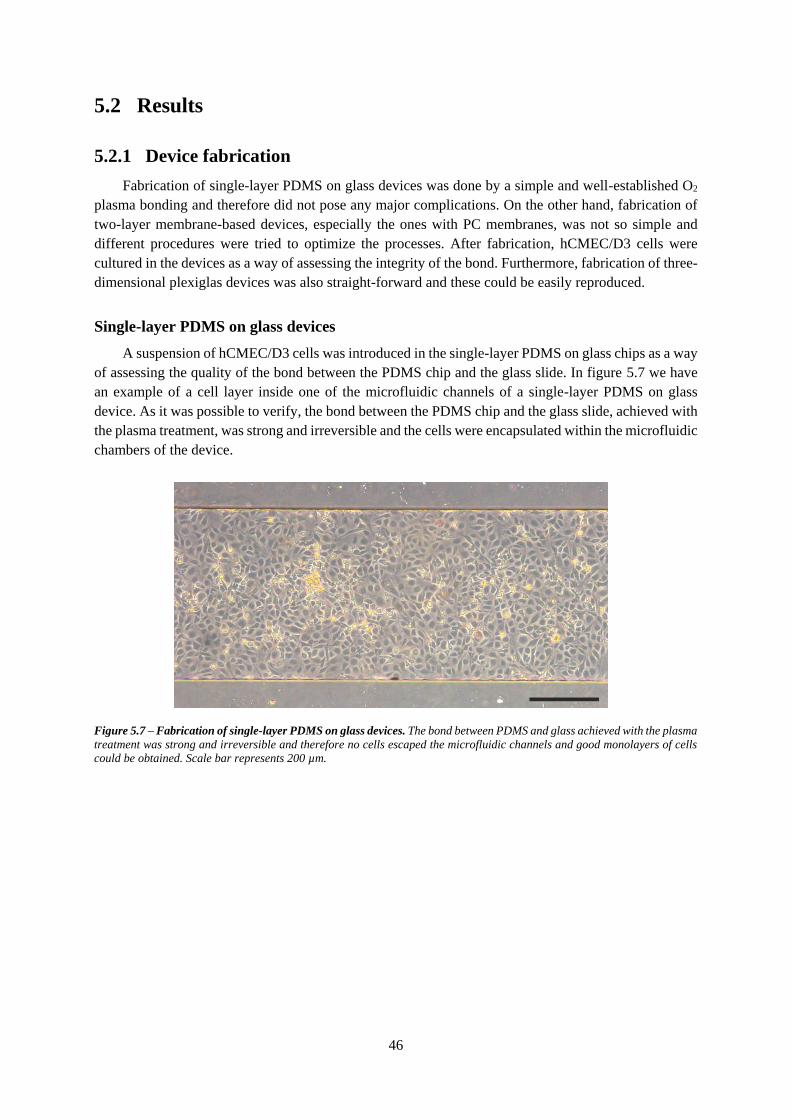
46
5.2 Results
5.2.1 Device fabrication
Fabrication of single-layer PDMS on glass devices was done by a simple and well-established O2
plasma bonding and therefore did not pose any major complications. On the other hand, fabrication of
two-layer membrane-based devices, especially the ones with PC membranes, was not so simple and
different procedures were tried to optimize the processes. After fabrication, hCMEC/D3 cells were
cultured in the devices as a way of assessing the integrity of the bond. Furthermore, fabrication of three-
dimensional plexiglas devices was also straight-forward and these could be easily reproduced.
Single-layer PDMS on glass devices
A suspension of hCMEC/D3 cells was introduced in the single-layer PDMS on glass chips as a way
of assessing the quality of the bond between the PDMS chip and the glass slide. In figure 5.7 we have
an example of a cell layer inside one of the microfluidic channels of a single-layer PDMS on glass
device. As it was possible to verify, the bond between the PDMS chip and the glass slide, achieved with
the plasma treatment, was strong and irreversible and the cells were encapsulated within the microfluidic
chambers of the device.
Figure 5.7 – Fabrication of single-layer PDMS on glass devices. The bond between PDMS and glass achieved with the plasma
treatment was strong and irreversible and therefore no cells escaped the microfluidic channels and good monolayers of cells
could be obtained. Scale bar represents 200 µm.
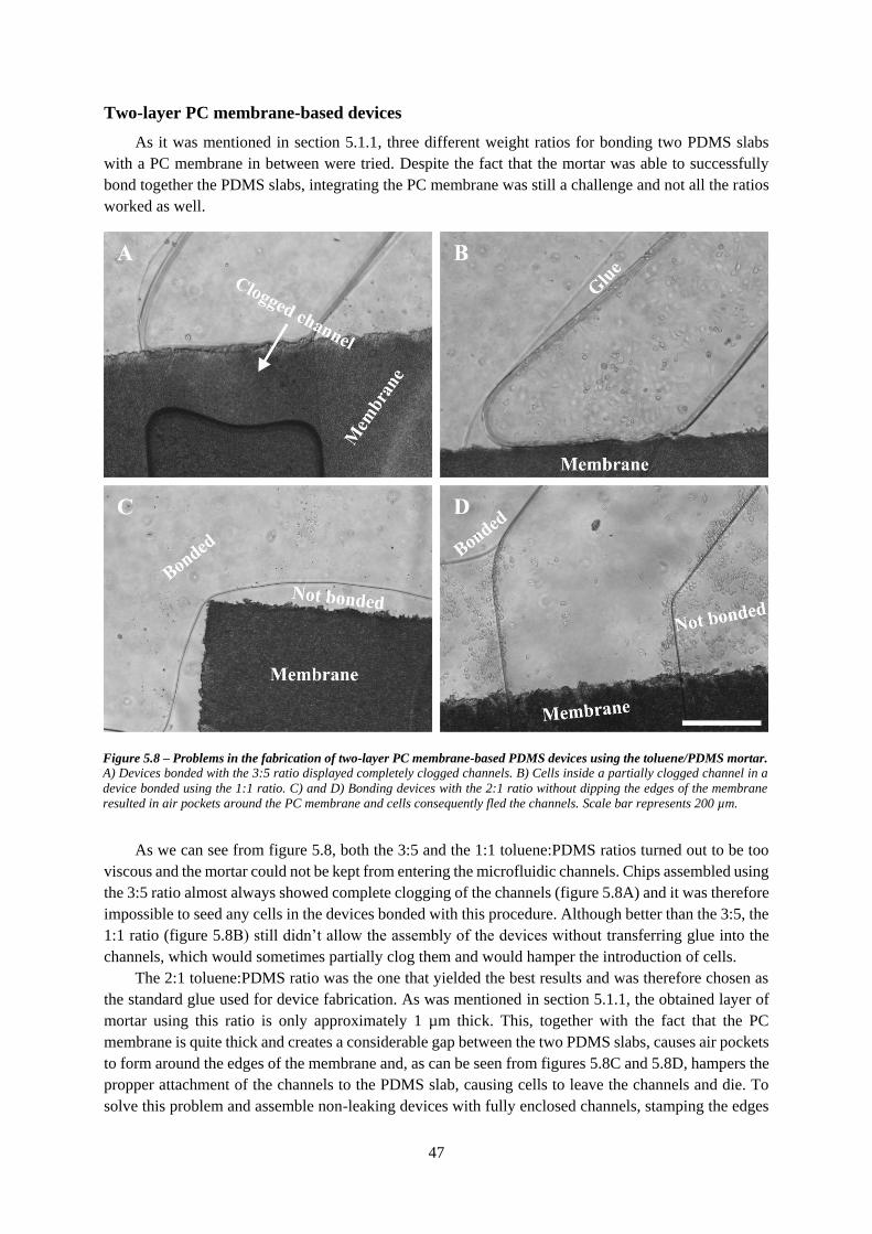
47
Two-layer PC membrane-based devices
As it was mentioned in section 5.1.1, three different weight ratios for bonding two PDMS slabs
with a PC membrane in between were tried. Despite the fact that the mortar was able to successfully
bond together the PDMS slabs, integrating the PC membrane was still a challenge and not all the ratios
worked as well.
As we can see from figure 5.8, both the 3:5 and the 1:1 toluene:PDMS ratios turned out to be too
viscous and the mortar could not be kept from entering the microfluidic channels. Chips assembled using
the 3:5 ratio almost always showed complete clogging of the channels (figure 5.8A) and it was therefore
impossible to seed any cells in the devices bonded with this procedure. Although better than the 3:5, the
1:1 ratio (figure 5.8B) still didn’t allow the assembly of the devices without transferring glue into the
channels, which would sometimes partially clog them and would hamper the introduction of cells.
The 2:1 toluene:PDMS ratio was the one that yielded the best results and was therefore chosen as
the standard glue used for device fabrication. As was mentioned in section 5.1.1, the obtained layer of
mortar using this ratio is only approximately 1 µm thick. This, together with the fact that the PC
membrane is quite thick and creates a considerable gap between the two PDMS slabs, causes air pockets
to form around the edges of the membrane and, as can be seen from figures 5.8C and 5.8D, hampers the
propper attachment of the channels to the PDMS slab, causing cells to leave the channels and die. To
solve this problem and assemble non-leaking devices with fully enclosed channels, stamping the edges
Figure 5.8 – Problems in the fabrication of two-layer PC membrane-based PDMS devices using the toluene/PDMS mortar. A) Devices bonded with the 3:5 ratio displayed completely clogged channels. B) Cells inside a partially clogged channel in a
device bonded using the 1:1 ratio. C) and D) Bonding devices with the 2:1 ratio without dipping the edges of the membrane
resulted in air pockets around the PC membrane and cells consequently fled the channels. Scale bar represents 200 µm.
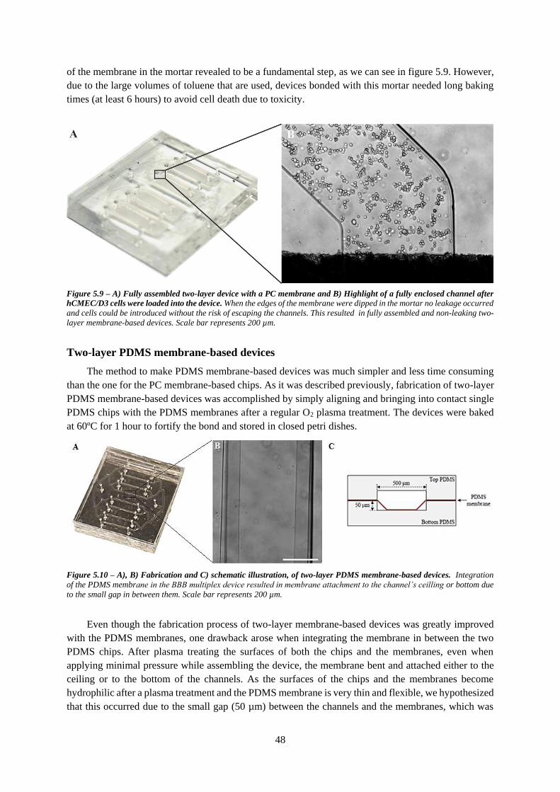
48
of the membrane in the mortar revealed to be a fundamental step, as we can see in figure 5.9. However,
due to the large volumes of toluene that are used, devices bonded with this mortar needed long baking
times (at least 6 hours) to avoid cell death due to toxicity.
Two-layer PDMS membrane-based devices
The method to make PDMS membrane-based devices was much simpler and less time consuming
than the one for the PC membrane-based chips. As it was described previously, fabrication of two-layer
PDMS membrane-based devices was accomplished by simply aligning and bringing into contact single
PDMS chips with the PDMS membranes after a regular O2 plasma treatment. The devices were baked
at 60ºC for 1 hour to fortify the bond and stored in closed petri dishes.
Even though the fabrication process of two-layer membrane-based devices was greatly improved
with the PDMS membranes, one drawback arose when integrating the membrane in between the two
PDMS chips. After plasma treating the surfaces of both the chips and the membranes, even when
applying minimal pressure while assembling the device, the membrane bent and attached either to the
ceiling or to the bottom of the channels. As the surfaces of the chips and the membranes become
hydrophilic after a plasma treatment and the PDMS membrane is very thin and flexible, we hypothesized
that this occurred due to the small gap (50 µm) between the channels and the membranes, which was
Figure 5.9 – A) Fully assembled two-layer device with a PC membrane and B) Highlight of a fully enclosed channel after
hCMEC/D3 cells were loaded into the device. When the edges of the membrane were dipped in the mortar no leakage occurred
and cells could be introduced without the risk of escaping the channels. This resulted in fully assembled and non-leaking two-
layer membrane-based devices. Scale bar represents 200 µm.
Figure 5.10 – A), B) Fabrication and C) schematic illustration, of two-layer PDMS membrane-based devices. Integration
of the PDMS membrane in the BBB multiplex device resulted in membrane attachment to the channel’s ceilling or bottom due
to the small gap in between them. Scale bar represents 200 µm.

49
not deep enough to prevent the PDMS surfaces from attracting and bonding to each other. To verify this,
single BBB-on-chip devices with a channel height of approximately 350 µm were fabricated and PDMS
membranes were integrated in them to check if the membrane would still attach either to the ceiling or
to the bottom of the channels after integrated in the devices.
As can be seen from figure 5.11, no attachment between the ceiling or the bottom of the PDMS
chips and the membranes was observed and a free-standing membrane was incorporated in the device.
This confirmed the initial hypothesis that free-standing membranes can only be incorporated in the
devices if the channels are deep enough to prevent the membrane from sticking to the channel’s ceiling
or bottom after activation in the plasma cleaner. In this way, it could be of interest to slightly increase
the height of the channels of the BBB-multiplex device to overcome this.
Lastly, the process to assemble two-layer PDMS membrane-based devices with Pt electrodes was
really similar to the one to assemble devices without electrodes, only a bit more time consuming as
placing the electrodes could be challenging.
Figure 5.11 – A), B) Single BBB device with a PDMS membrane and C) respective schematic illustration. When integrated
in the single BBB device, which has ±8 times higher channels, the membrane was free-standing. Scale bar represents 200 µm.
Figure 5.12 – Fully assembled two-layer PDMS membrane-based device with Pt electrodes.
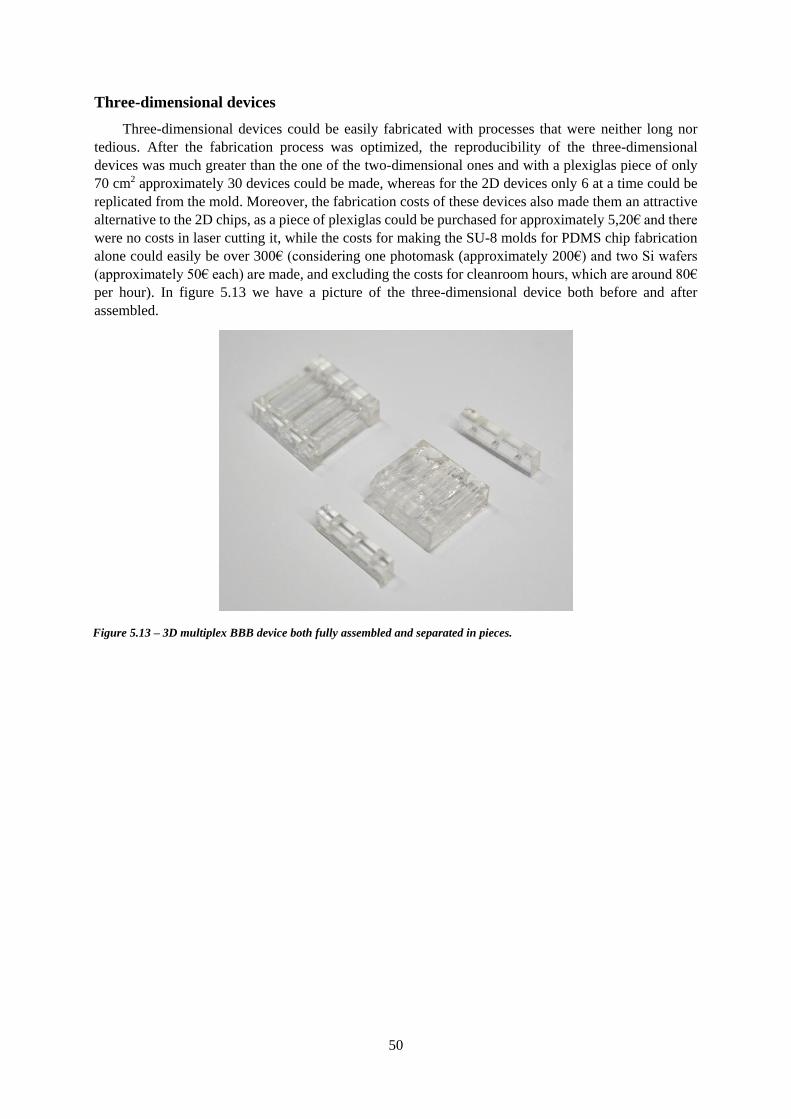
50
Three-dimensional devices
Three-dimensional devices could be easily fabricated with processes that were neither long nor
tedious. After the fabrication process was optimized, the reproducibility of the three-dimensional
devices was much greater than the one of the two-dimensional ones and with a plexiglas piece of only
70 cm2 approximately 30 devices could be made, whereas for the 2D devices only 6 at a time could be
replicated from the mold. Moreover, the fabrication costs of these devices also made them an attractive
alternative to the 2D chips, as a piece of plexiglas could be purchased for approximately 5,20€ and there
were no costs in laser cutting it, while the costs for making the SU-8 molds for PDMS chip fabrication
alone could easily be over 300€ (considering one photomask (approximately 200€) and two Si wafers
(approximately 50€ each) are made, and excluding the costs for cleanroom hours, which are around 80€
per hour). In figure 5.13 we have a picture of the three-dimensional device both before and after
assembled.
Figure 5.13 – 3D multiplex BBB device both fully assembled and separated in pieces.
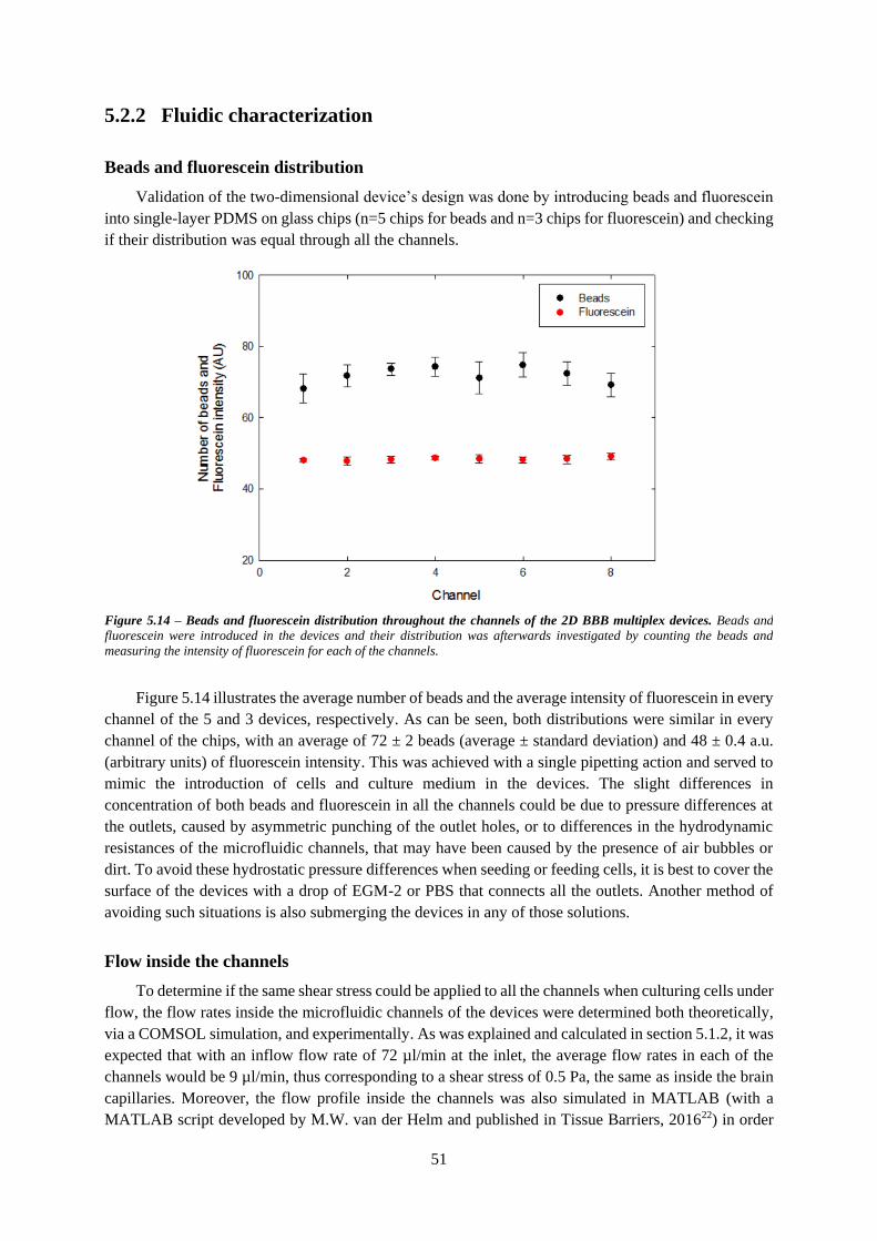
51
5.2.2 Fluidic characterization
Beads and fluorescein distribution
Validation of the two-dimensional device’s design was done by introducing beads and fluorescein
into single-layer PDMS on glass chips (n=5 chips for beads and n=3 chips for fluorescein) and checking
if their distribution was equal through all the channels.
Figure 5.14 illustrates the average number of beads and the average intensity of fluorescein in every
channel of the 5 and 3 devices, respectively. As can be seen, both distributions were similar in every
channel of the chips, with an average of 72 ± 2 beads (average ± standard deviation) and 48 ± 0.4 a.u.
(arbitrary units) of fluorescein intensity. This was achieved with a single pipetting action and served to
mimic the introduction of cells and culture medium in the devices. The slight differences in
concentration of both beads and fluorescein in all the channels could be due to pressure differences at
the outlets, caused by asymmetric punching of the outlet holes, or to differences in the hydrodynamic
resistances of the microfluidic channels, that may have been caused by the presence of air bubbles or
dirt. To avoid these hydrostatic pressure differences when seeding or feeding cells, it is best to cover the
surface of the devices with a drop of EGM-2 or PBS that connects all the outlets. Another method of
avoiding such situations is also submerging the devices in any of those solutions.
Flow inside the channels
To determine if the same shear stress could be applied to all the channels when culturing cells under
flow, the flow rates inside the microfluidic channels of the devices were determined both theoretically,
via a COMSOL simulation, and experimentally. As was explained and calculated in section 5.1.2, it was
expected that with an inflow flow rate of 72 µl/min at the inlet, the average flow rates in each of the
channels would be 9 µl/min, thus corresponding to a shear stress of 0.5 Pa, the same as inside the brain
capillaries. Moreover, the flow profile inside the channels was also simulated in MATLAB (with a
MATLAB script developed by M.W. van der Helm and published in Tissue Barriers, 201622) in order
Figure 5.14 – Beads and fluorescein distribution throughout the channels of the 2D BBB multiplex devices. Beads and
fluorescein were introduced in the devices and their distribution was afterwards investigated by counting the beads and
measuring the intensity of fluorescein for each of the channels.
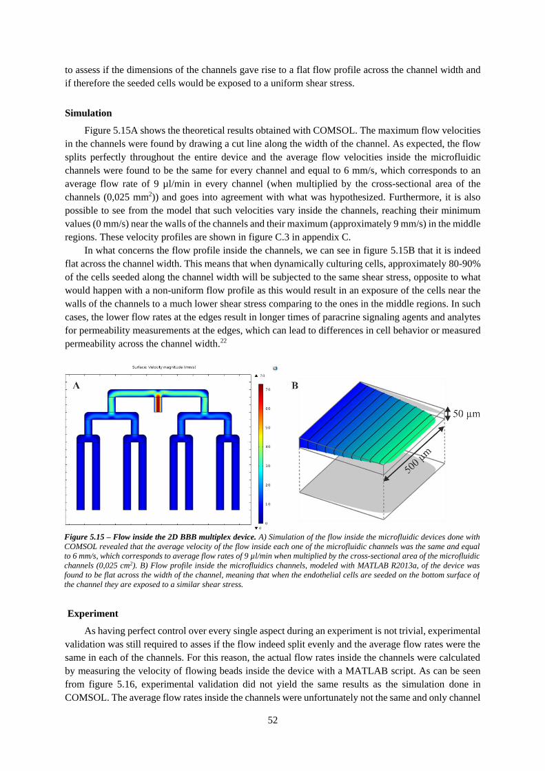
52
to assess if the dimensions of the channels gave rise to a flat flow profile across the channel width and
if therefore the seeded cells would be exposed to a uniform shear stress.
Simulation
Figure 5.15A shows the theoretical results obtained with COMSOL. The maximum flow velocities
in the channels were found by drawing a cut line along the width of the channel. As expected, the flow
splits perfectly throughout the entire device and the average flow velocities inside the microfluidic
channels were found to be the same for every channel and equal to 6 mm/s, which corresponds to an
average flow rate of 9 µl/min in every channel (when multiplied by the cross-sectional area of the
channels (0,025 mm2)) and goes into agreement with what was hypothesized. Furthermore, it is also
possible to see from the model that such velocities vary inside the channels, reaching their minimum
values (0 mm/s) near the walls of the channels and their maximum (approximately 9 mm/s) in the middle
regions. These velocity profiles are shown in figure C.3 in appendix C.
In what concerns the flow profile inside the channels, we can see in figure 5.15B that it is indeed
flat across the channel width. This means that when dynamically culturing cells, approximately 80-90%
of the cells seeded along the channel width will be subjected to the same shear stress, opposite to what
would happen with a non-uniform flow profile as this would result in an exposure of the cells near the
walls of the channels to a much lower shear stress comparing to the ones in the middle regions. In such
cases, the lower flow rates at the edges result in longer times of paracrine signaling agents and analytes
for permeability measurements at the edges, which can lead to differences in cell behavior or measured
permeability across the channel width.22
Experiment
As having perfect control over every single aspect during an experiment is not trivial, experimental
validation was still required to asses if the flow indeed split evenly and the average flow rates were the
same in each of the channels. For this reason, the actual flow rates inside the channels were calculated
by measuring the velocity of flowing beads inside the device with a MATLAB script. As can be seen
from figure 5.16, experimental validation did not yield the same results as the simulation done in
COMSOL. The average flow rates inside the channels were unfortunately not the same and only channel
Figure 5.15 – Flow inside the 2D BBB multiplex device. A) Simulation of the flow inside the microfluidic devices done with
COMSOL revealed that the average velocity of the flow inside each one of the microfluidic channels was the same and equal
to 6 mm/s, which corresponds to average flow rates of 9 µl/min when multiplied by the cross-sectional area of the microfluidic
channels (0,025 cm2). B) Flow profile inside the microfluidics channels, modeled with MATLAB R2013a, of the device was
found to be flat across the width of the channel, meaning that when the endothelial cells are seeded on the bottom surface of
the channel they are exposed to a similar shear stress.

53
8 had an average flow rate close to 9 µl/min. This could be derived from many situations, such as
differences in the hydrodynamic resistances of the microfluidic channels, caused by the presence of
trapped air inside them, differences in hydrostatic pressure at the outlets, which may have been caused
by not punching the outlets of the device in the exact same place, or by differences in the homogeneity
of the medium drop on top of the device, or even due to irregularities in the SU-8 structures in the mold
from which the chips were replicated. Besides these reasons, the number of tracked beads and the
analysis method might have also influenced the results. For instance, if the majority of the tracked beads
were flowing closer to the walls of a channel, the calculated average velocity of those beads will be
smaller as velocity is minimum closer to the walls of a channel. This goes into agreement with the
simulation done in COMSOL, as we can see from figure 5.15A and from the velocity profiles depicted
in figure C.1 in appendix C, and would therefore result in smaller flow rates when comparing to channels
where most of the beads were tracked in the middle regions. The measured values of the average flow
rates obtained both theoretically and empirically are summarized in table 5.1.
Channel Simulation Experiment
Q (µl/min) τ (Pa) Q (µl/min) τ (Pa)
1 9.0 0.5 7.8 0.4
2 9.0 0.5 11.7 0.7
3 9.0 0.5 7.7 0.4
4 9.0 0.5 6.5 0.4
5 9.0 0.5 8.2 0.5
6 9.0 0.5 13.3 0.7
7 9.0 0.5 7.9 0.4
8 9.0 0.5 9.1 0.5
Table 5.1 – Measured average flow rates, and corresponding calculated shear rates, inside the microfluidic channels.
Differences in the empiric measurements may be due differences in the hydrodynamic resistances of the channels, as well as
to hydrostatic pressure differences between the outlets.
Figure 5.16 – Flow rates inside the microfluidic devices obtained empirically. The device was connected to a Nemesys syringe
pump, equipped with a 3 ml BD syringe, with Tygon tubing and metal syringe tips. Average flow rates were calculated from
the average velocities of the flowing beads with a MATLAB script, and were found to unfortunately vary from channel to
channel.
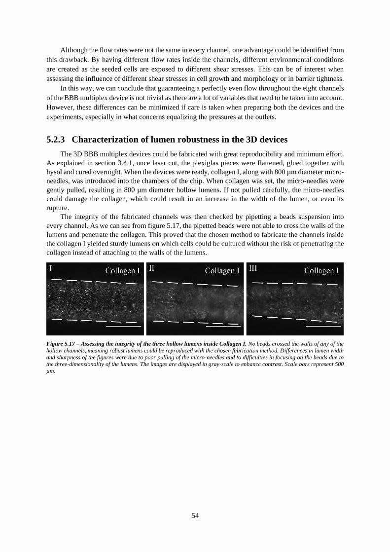
54
Although the flow rates were not the same in every channel, one advantage could be identified from
this drawback. By having different flow rates inside the channels, different environmental conditions
are created as the seeded cells are exposed to different shear stresses. This can be of interest when
assessing the influence of different shear stresses in cell growth and morphology or in barrier tightness.
In this way, we can conclude that guaranteeing a perfectly even flow throughout the eight channels
of the BBB multiplex device is not trivial as there are a lot of variables that need to be taken into account.
However, these differences can be minimized if care is taken when preparing both the devices and the
experiments, especially in what concerns equalizing the pressures at the outlets.
5.2.3 Characterization of lumen robustness in the 3D devices
The 3D BBB multiplex devices could be fabricated with great reproducibility and minimum effort.
As explained in section 3.4.1, once laser cut, the plexiglas pieces were flattened, glued together with
hysol and cured overnight. When the devices were ready, collagen I, along with 800 µm diameter micro-
needles, was introduced into the chambers of the chip. When collagen was set, the micro-needles were
gently pulled, resulting in 800 µm diameter hollow lumens. If not pulled carefully, the micro-needles
could damage the collagen, which could result in an increase in the width of the lumen, or even its
rupture.
The integrity of the fabricated channels was then checked by pipetting a beads suspension into
every channel. As we can see from figure 5.17, the pipetted beads were not able to cross the walls of the
lumens and penetrate the collagen. This proved that the chosen method to fabricate the channels inside
the collagen I yielded sturdy lumens on which cells could be cultured without the risk of penetrating the
collagen instead of attaching to the walls of the lumens.
Figure 5.17 – Assessing the integrity of the three hollow lumens inside Collagen I. No beads crossed the walls of any of the
hollow channels, meaning robust lumens could be reproduced with the chosen fabrication method. Differences in lumen width
and sharpness of the figures were due to poor pulling of the micro-needles and to difficulties in focusing on the beads due to
the three-dimensionality of the lumens. The images are displayed in gray-scale to enhance contrast. Scale bars represent 500
µm.
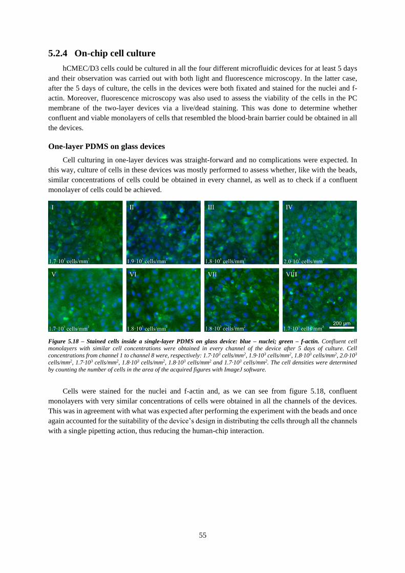
55
5.2.4 On-chip cell culture
hCMEC/D3 cells could be cultured in all the four different microfluidic devices for at least 5 days
and their observation was carried out with both light and fluorescence microscopy. In the latter case,
after the 5 days of culture, the cells in the devices were both fixated and stained for the nuclei and f-
actin. Moreover, fluorescence microscopy was also used to assess the viability of the cells in the PC
membrane of the two-layer devices via a live/dead staining. This was done to determine whether
confluent and viable monolayers of cells that resembled the blood-brain barrier could be obtained in all
the devices.
One-layer PDMS on glass devices
Cell culturing in one-layer devices was straight-forward and no complications were expected. In
this way, culture of cells in these devices was mostly performed to assess whether, like with the beads,
similar concentrations of cells could be obtained in every channel, as well as to check if a confluent
monolayer of cells could be achieved.
Cells were stained for the nuclei and f-actin and, as we can see from figure 5.18, confluent
monolayers with very similar concentrations of cells were obtained in all the channels of the devices.
This was in agreement with what was expected after performing the experiment with the beads and once
again accounted for the suitability of the device’s design in distributing the cells through all the channels
with a single pipetting action, thus reducing the human-chip interaction.
Figure 5.18 – Stained cells inside a single-layer PDMS on glass device: blue – nuclei; green – f-actin. Confluent cell
monolayers with similar cell concentrations were obtained in every channel of the device after 5 days of culture. Cell
concentrations from channel 1 to channel 8 were, respectively: 1.7·103 cells/mm2, 1.9·103 cells/mm2, 1.8·103 cells/mm2, 2.0·103
cells/mm2, 1.7·103 cells/mm2, 1.8·103 cells/mm2, 1.8·103 cells/mm2 and 1.7·103 cells/mm2. The cell densities were determined
by counting the number of cells in the area of the acquired figures with ImageJ software.
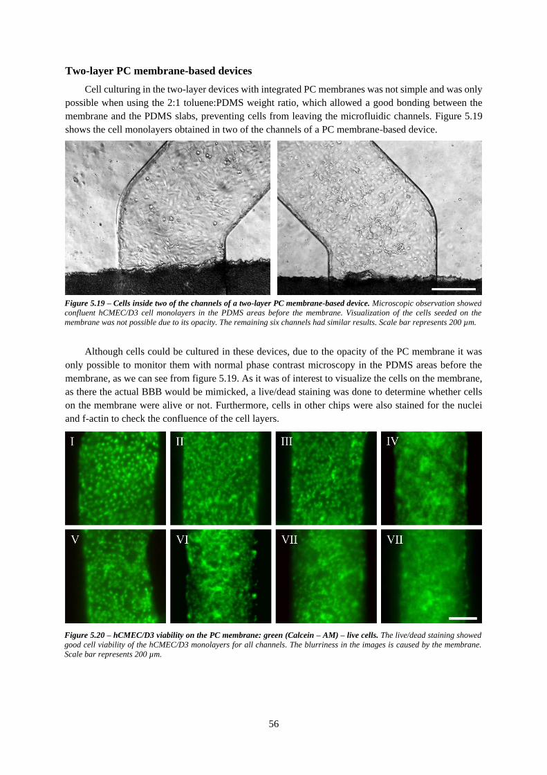
56
Two-layer PC membrane-based devices
Cell culturing in the two-layer devices with integrated PC membranes was not simple and was only
possible when using the 2:1 toluene:PDMS weight ratio, which allowed a good bonding between the
membrane and the PDMS slabs, preventing cells from leaving the microfluidic channels. Figure 5.19
shows the cell monolayers obtained in two of the channels of a PC membrane-based device.
Although cells could be cultured in these devices, due to the opacity of the PC membrane it was
only possible to monitor them with normal phase contrast microscopy in the PDMS areas before the
membrane, as we can see from figure 5.19. As it was of interest to visualize the cells on the membrane,
as there the actual BBB would be mimicked, a live/dead staining was done to determine whether cells
on the membrane were alive or not. Furthermore, cells in other chips were also stained for the nuclei
and f-actin to check the confluence of the cell layers.
Figure 5.20 – hCMEC/D3 viability on the PC membrane: green (Calcein – AM) – live cells. The live/dead staining showed
good cell viability of the hCMEC/D3 monolayers for all channels. The blurriness in the images is caused by the membrane.
Scale bar represents 200 µm.
Figure 5.19 – Cells inside two of the channels of a two-layer PC membrane-based device. Microscopic observation showed
confluent hCMEC/D3 cell monolayers in the PDMS areas before the membrane. Visualization of the cells seeded on the
membrane was not possible due to its opacity. The remaining six channels had similar results. Scale bar represents 200 µm.
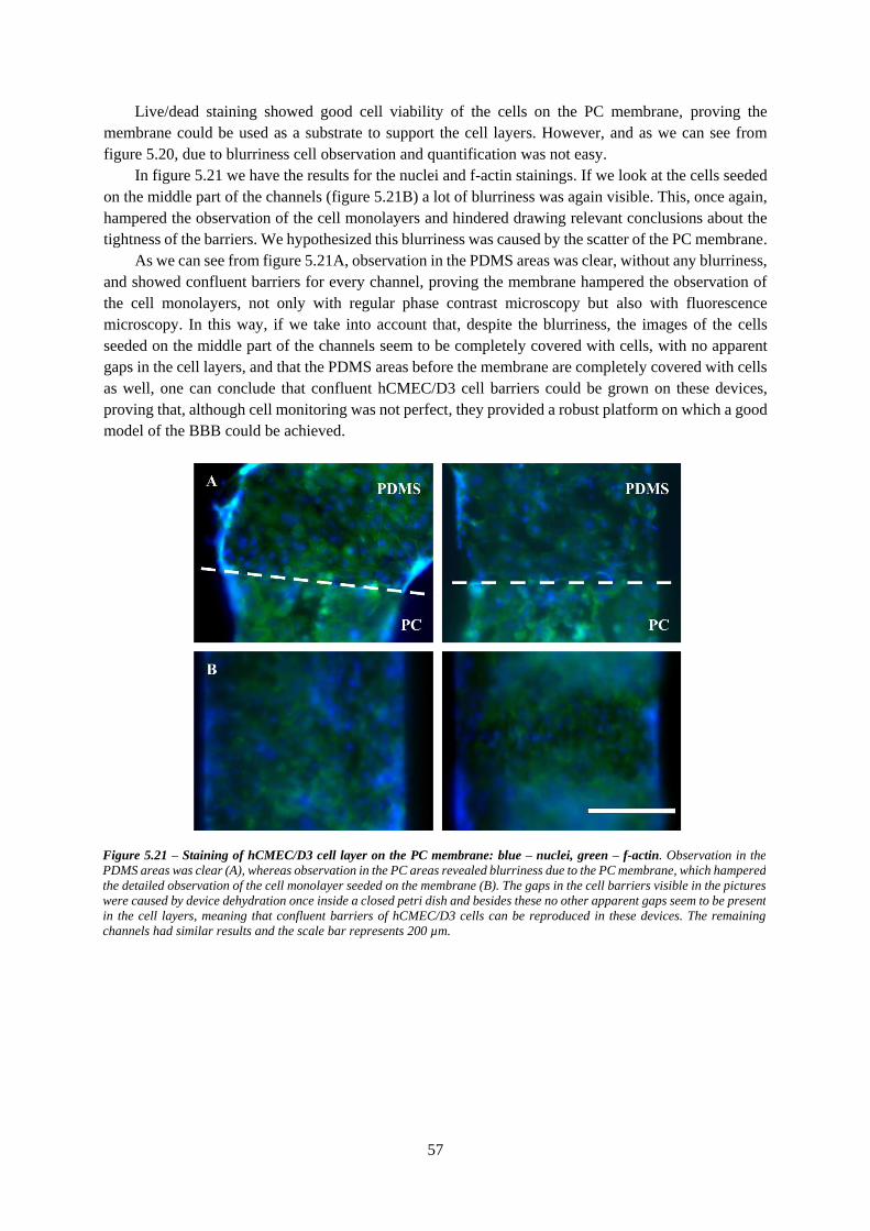
57
Live/dead staining showed good cell viability of the cells on the PC membrane, proving the
membrane could be used as a substrate to support the cell layers. However, and as we can see from
figure 5.20, due to blurriness cell observation and quantification was not easy.
In figure 5.21 we have the results for the nuclei and f-actin stainings. If we look at the cells seeded
on the middle part of the channels (figure 5.21B) a lot of blurriness was again visible. This, once again,
hampered the observation of the cell monolayers and hindered drawing relevant conclusions about the
tightness of the barriers. We hypothesized this blurriness was caused by the scatter of the PC membrane.
As we can see from figure 5.21A, observation in the PDMS areas was clear, without any blurriness,
and showed confluent barriers for every channel, proving the membrane hampered the observation of
the cell monolayers, not only with regular phase contrast microscopy but also with fluorescence
microscopy. In this way, if we take into account that, despite the blurriness, the images of the cells
seeded on the middle part of the channels seem to be completely covered with cells, with no apparent
gaps in the cell layers, and that the PDMS areas before the membrane are completely covered with cells
as well, one can conclude that confluent hCMEC/D3 cell barriers could be grown on these devices,
proving that, although cell monitoring was not perfect, they provided a robust platform on which a good
model of the BBB could be achieved.
Figure 5.21 – Staining of hCMEC/D3 cell layer on the PC membrane: blue – nuclei, green – f-actin. Observation in the
PDMS areas was clear (A), whereas observation in the PC areas revealed blurriness due to the PC membrane, which hampered
the detailed observation of the cell monolayer seeded on the membrane (B). The gaps in the cell barriers visible in the pictures
were caused by device dehydration once inside a closed petri dish and besides these no other apparent gaps seem to be present
in the cell layers, meaning that confluent barriers of hCMEC/D3 cells can be reproduced in these devices. The remaining
channels had similar results and the scale bar represents 200 µm.
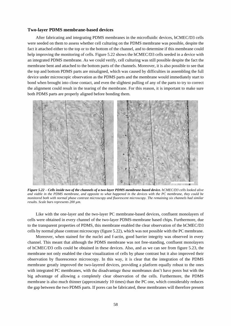
58
Two-layer PDMS membrane-based devices
After fabricating and integrating PDMS membranes in the microfluidic devices, hCMEC/D3 cells
were seeded on them to assess whether cell culturing on the PDMS membrane was possible, despite the
fact it attached either to the top or to the bottom of the channel, and to determine if this membrane could
help improving the monitoring of cells. Figure 5.22 shows the hCMEC/D3 cells seeded in a device with
an integrated PDMS membrane. As we could verify, cell culturing was still possible despite the fact the
membrane bent and attached to the bottom parts of the channels. Moreover, it is also possible to see that
the top and bottom PDMS parts are misaligned, which was caused by difficulties in assembling the full
device under microscopic observation as the PDMS parts and the membrane would immediately start to
bond when brought into close contact, and even the slightest pulling of any of the parts to try to correct
the alignment could result in the tearing of the membrane. For this reason, it is important to make sure
both PDMS parts are properly aligned before bonding them.
Like with the one-layer and the two-layer PC membrane-based devices, confluent monolayers of
cells were obtained in every channel of the two-layer PDMS-membrane based chips. Furthermore, due
to the transparent properties of PDMS, this membrane enabled the clear observation of the hCMEC/D3
cells by normal phase contrast microscopy (figure 5.22), which was not possible with the PC membrane.
Moreover, when stained for the nuclei and f-actin, good barrier integrity was observed in every
channel. This meant that although the PDMS membrane was not free-standing, confluent monolayers
of hCMEC/D3 cells could be obtained in these devices. Also, and as we can see from figure 5.23, the
membrane not only enabled the clear visualization of cells by phase contrast but it also improved their
observation by fluorescence microscopy. In this way, it is clear that the integration of the PDMS
membrane greatly improved the two-layered devices, providing a platform equally robust to the ones
with integrated PC membranes, with the disadvantage these membranes don’t have pores but with the
big advantage of allowing a completely clear observation of the cells. Furthermore, the PDMS
membrane is also much thinner (approximately 10 times) than the PC one, which considerably reduces
the gap between the two PDMS parts. If pores can be fabricated, these membranes will therefore present
Figure 5.22 – Cells inside two of the channels of a two-layer PDMS membrane-based device. hCMEC/D3 cells looked alive
and viable in the PDMS membrane, and opposite to what happened in the devices with the PC membrane, they could be
monitored both with normal phase contrast microscopy and fluorescent microscopy. The remaining six channels had similar
results. Scale bars represents 200 µm.
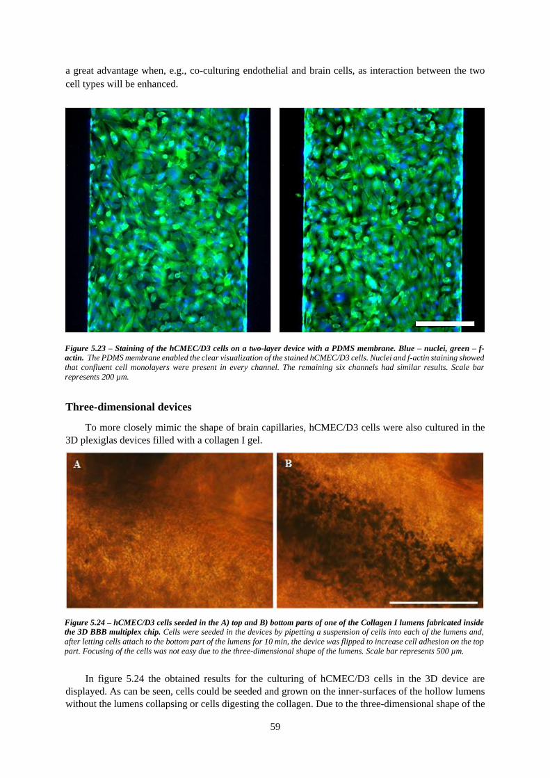
59
a great advantage when, e.g., co-culturing endothelial and brain cells, as interaction between the two
cell types will be enhanced.
Three-dimensional devices
To more closely mimic the shape of brain capillaries, hCMEC/D3 cells were also cultured in the
3D plexiglas devices filled with a collagen I gel.
In figure 5.24 the obtained results for the culturing of hCMEC/D3 cells in the 3D device are
displayed. As can be seen, cells could be seeded and grown on the inner-surfaces of the hollow lumens
without the lumens collapsing or cells digesting the collagen. Due to the three-dimensional shape of the
Figure 5.23 – Staining of the hCMEC/D3 cells on a two-layer device with a PDMS membrane. Blue – nuclei, green – f-
actin. The PDMS membrane enabled the clear visualization of the stained hCMEC/D3 cells. Nuclei and f-actin staining showed
that confluent cell monolayers were present in every channel. The remaining six channels had similar results. Scale bar
represents 200 µm.
Figure 5.24 – hCMEC/D3 cells seeded in the A) top and B) bottom parts of one of the Collagen I lumens fabricated inside
the 3D BBB multiplex chip. Cells were seeded in the devices by pipetting a suspension of cells into each of the lumens and,
after letting cells attach to the bottom part of the lumens for 10 min, the device was flipped to increase cell adhesion on the top
part. Focusing of the cells was not easy due to the three-dimensional shape of the lumens. Scale bar represents 500 µm.
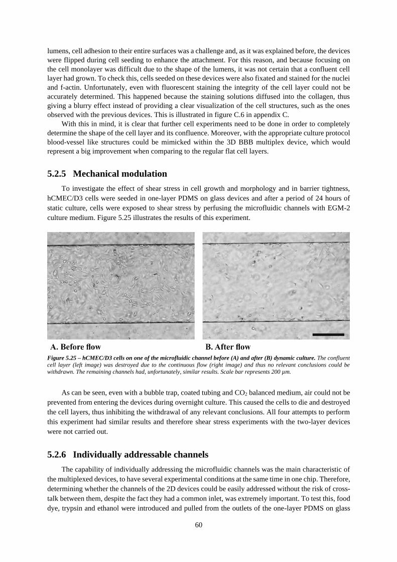
60
lumens, cell adhesion to their entire surfaces was a challenge and, as it was explained before, the devices
were flipped during cell seeding to enhance the attachment. For this reason, and because focusing on
the cell monolayer was difficult due to the shape of the lumens, it was not certain that a confluent cell
layer had grown. To check this, cells seeded on these devices were also fixated and stained for the nuclei
and f-actin. Unfortunately, even with fluorescent staining the integrity of the cell layer could not be
accurately determined. This happened because the staining solutions diffused into the collagen, thus
giving a blurry effect instead of providing a clear visualization of the cell structures, such as the ones
observed with the previous devices. This is illustrated in figure C.6 in appendix C.
With this in mind, it is clear that further cell experiments need to be done in order to completely
determine the shape of the cell layer and its confluence. Moreover, with the appropriate culture protocol
blood-vessel like structures could be mimicked within the 3D BBB multiplex device, which would
represent a big improvement when comparing to the regular flat cell layers.
5.2.5 Mechanical modulation
To investigate the effect of shear stress in cell growth and morphology and in barrier tightness,
hCMEC/D3 cells were seeded in one-layer PDMS on glass devices and after a period of 24 hours of
static culture, cells were exposed to shear stress by perfusing the microfluidic channels with EGM-2
culture medium. Figure 5.25 illustrates the results of this experiment.
As can be seen, even with a bubble trap, coated tubing and CO2 balanced medium, air could not be
prevented from entering the devices during overnight culture. This caused the cells to die and destroyed
the cell layers, thus inhibiting the withdrawal of any relevant conclusions. All four attempts to perform
this experiment had similar results and therefore shear stress experiments with the two-layer devices
were not carried out.
5.2.6 Individually addressable channels
The capability of individually addressing the microfluidic channels was the main characteristic of
the multiplexed devices, to have several experimental conditions at the same time in one chip. Therefore,
determining whether the channels of the 2D devices could be easily addressed without the risk of cross-
talk between them, despite the fact they had a common inlet, was extremely important. To test this, food
dye, trypsin and ethanol were introduced and pulled from the outlets of the one-layer PDMS on glass
Figure 5.25 – hCMEC/D3 cells on one of the microfluidic channel before (A) and after (B) dynamic culture. The confluent
cell layer (left image) was destroyed due to the continuous flow (right image) and thus no relevant conclusions could be
withdrawn. The remaining channels had, unfortunately, similar results. Scale bar represents 200 µm.
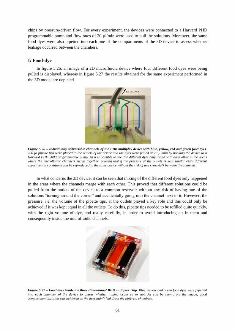
61
chips by pressure-driven flow. For every experiment, the devices were connected to a Harvard PHD
programmable pump and flow rates of 20 µl/min were used to pull the solutions. Moreover, the same
food dyes were also pipetted into each one of the compartments of the 3D device to assess whether
leakage occurred between the chambers.
I: Food-dye
In figure 5.26, an image of a 2D microfluidic device where four different food dyes were being
pulled is displayed, whereas in figure 5.27 the results obtained for the same experiment performed in
the 3D model are depicted.
In what concerns the 2D device, it can be seen that mixing of the different food dyes only happened
in the areas where the channels merge with each other. This proved that different solutions could be
pulled from the outlets of the device to a common reservoir without any risk of having one of the
solutions “turning around the corner” and accidentally going into the channel next to it. However, the
pressure, i.e. the volume of the pipette tips, at the outlets played a key role and this could only be
achieved if it was kept equal in all the outlets. To do this, pipette tips needed to be refilled quite quickly,
with the right volume of dye, and really carefully, in order to avoid introducing air in them and
consequently inside the microfluidic channels.
Figure 5.26 – Individually addressable channels of the BBB multiplex device with blue, yellow, red and green food dyes. 200 µl pipette tips were placed in the outlets of the device and the dyes were pulled at 20 µl/min by hooking the device to a
Harvard PHD 2000 programmable pump. As it is possible to see, the different dyes only mixed with each other in the areas
where the microfluidic channels merge together, proving that if the pressure at the outlets is kept similar eight different
experimental conditions can be reproduced in the same device without the risk of any cross-talk between the channels.
Figure 5.27 – Food dyes inside the three-dimensional BBB multiplex chip. Blue, yellow and green food dyes were pipetted
into each chamber of the device to assess whether mixing occurred or not. As can be seen from the image, good
compartmentalization was achieved as the dyes didn’t leak from the different chambers.
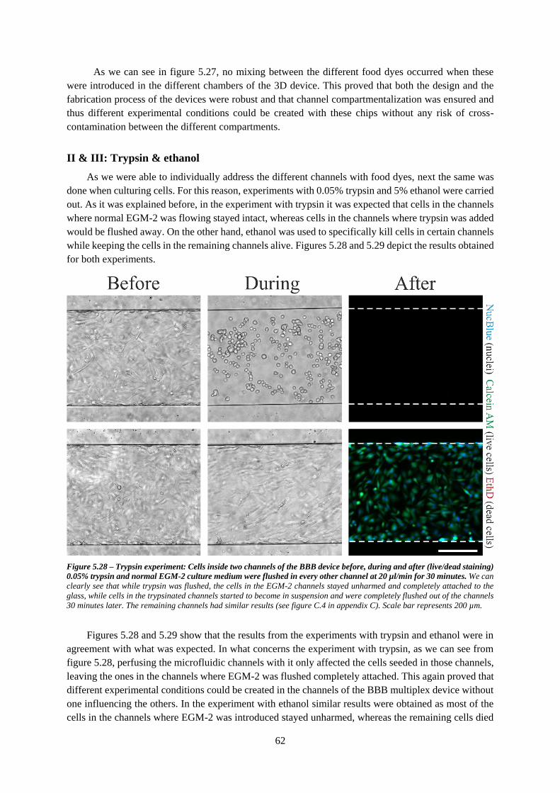
62
As we can see in figure 5.27, no mixing between the different food dyes occurred when these
were introduced in the different chambers of the 3D device. This proved that both the design and the
fabrication process of the devices were robust and that channel compartmentalization was ensured and
thus different experimental conditions could be created with these chips without any risk of cross-
contamination between the different compartments.
II & III: Trypsin & ethanol
As we were able to individually address the different channels with food dyes, next the same was
done when culturing cells. For this reason, experiments with 0.05% trypsin and 5% ethanol were carried
out. As it was explained before, in the experiment with trypsin it was expected that cells in the channels
where normal EGM-2 was flowing stayed intact, whereas cells in the channels where trypsin was added
would be flushed away. On the other hand, ethanol was used to specifically kill cells in certain channels
while keeping the cells in the remaining channels alive. Figures 5.28 and 5.29 depict the results obtained
for both experiments.
Figures 5.28 and 5.29 show that the results from the experiments with trypsin and ethanol were in
agreement with what was expected. In what concerns the experiment with trypsin, as we can see from
figure 5.28, perfusing the microfluidic channels with it only affected the cells seeded in those channels,
leaving the ones in the channels where EGM-2 was flushed completely attached. This again proved that
different experimental conditions could be created in the channels of the BBB multiplex device without
one influencing the others. In the experiment with ethanol similar results were obtained as most of the
cells in the channels where EGM-2 was introduced stayed unharmed, whereas the remaining cells died
Figure 5.28 – Trypsin experiment: Cells inside two channels of the BBB device before, during and after (live/dead staining)
0.05% trypsin and normal EGM-2 culture medium were flushed in every other channel at 20 µl/min for 30 minutes. We can
clearly see that while trypsin was flushed, the cells in the EGM-2 channels stayed unharmed and completely attached to the
glass, while cells in the trypsinated channels started to become in suspension and were completely flushed out of the channels
30 minutes later. The remaining channels had similar results (see figure C.4 in appendix C). Scale bar represents 200 µm.
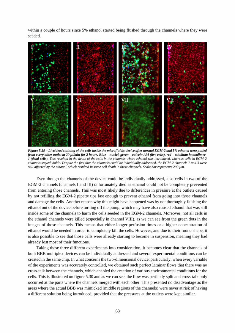
63
within a couple of hours since 5% ethanol started being flushed through the channels where they were
seeded.
Even though the channels of the device could be individually addressed, also cells in two of the
EGM-2 channels (channels I and III) unfortunately died as ethanol could not be completely prevented
from entering those channels. This was most likely due to differences in pressure at the outlets caused
by not refilling the EGM-2 pipette tips fast enough to prevent ethanol from going into those channels
and damage the cells. Another reason why this might have happened was by not thoroughly flushing the
ethanol out of the device before turning off the pump, which may have also caused ethanol that was still
inside some of the channels to harm the cells seeded in the EGM-2 channels. Moreover, not all cells in
the ethanol channels were killed (especially in channel VIII), as we can see from the green dots in the
images of those channels. This means that either longer perfusion times or a higher concentration of
ethanol would be needed in order to completely kill the cells. However, and due to their round shape, it
is also possible to see that those cells were already starting to become in suspension, meaning they had
already lost most of their functions.
Taking these three different experiments into consideration, it becomes clear that the channels of
both BBB multiplex devices can be individually addressed and several experimental conditions can be
created in the same chip. In what concerns the two-dimensional device, particularly, when every variable
of the experiments was accurately controlled, we obtained such perfect laminar flows that there was no
cross-talk between the channels, which enabled the creation of various environmental conditions for the
cells. This is illustrated on figure 5.30 and as we can see, the flow was perfectly split and cross-talk only
occurred at the parts where the channels merged with each other. This presented no disadvantage as the
areas where the actual BBB was mimicked (middle regions of the channels) were never at risk of having
a different solution being introduced, provided that the pressures at the outlets were kept similar.
Figure 5.29 – Live/dead staining of the cells inside the microfluidic device after normal EGM-2 and 5% ethanol were pulled
from every other outlet at 20 µl/min for 2 hours. Blue – nuclei, green – calcein AM (live cells), red – ethidium homodimer-
1 (dead cells). This resulted in the death of the cells in the channels where ethanol was introduced, whereas cells in EGM-2
channels stayed viable. Despite the fact that the channels could be individually addressed, the EGM-2 channels 1 and 3 were
still affected by the ethanol, which resulted in some cell death in these channels. Scale bar represents 200 µm.
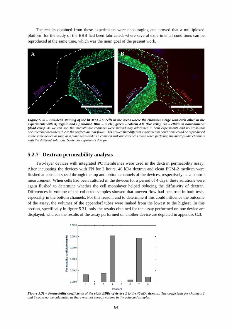
64
The results obtained from these experiments were encouraging and proved that a multiplexed
platform for the study of the BBB had been fabricated, where several experimental conditions can be
reproduced at the same time, which was the main goal of the present work.
5.2.7 Dextran permeability analysis
Two-layer devices with integrated PC membranes were used in the dextran permeability assay.
After incubating the devices with FN for 2 hours, 40 kDa dextran and clean EGM-2 medium were
flushed at constant speed through the top and bottom channels of the devices, respectively, as a control
measurement. When cells had been cultured in the devices for a period of 4 days, these solutions were
again flushed to determine whether the cell monolayer helped reducing the diffusivity of dextran.
Differences in volume of the collected samples showed that uneven flow had occurred in both tests,
especially in the bottom channels. For this reason, and to determine if this could influence the outcome
of the assay, the volumes of the eppendorf tubes were ranked from the lowest to the highest. In this
section, specifically in figure 5.31, only the results obtained for the assay performed on one device are
displayed, whereas the results of the assay performed on another device are depicted in appendix C.3.
Figure 5.30 – Live/dead staining of the hCMEC/D3 cells in the areas where the channels merge with each other in the
experiments with A) trypsin and B) ethanol. Blue – nuclei, green – calcein AM (live cells), red – ethidium homodimer-1
(dead cells). As we can see, the microfluidic channels were individually addressed in both experiments and no cross-talk
occurred between them due to the perfect laminar flows. This proved that different experimental conditions could be reproduced
in the same device as long as a pump was used as a common sink and care was taken when perfusing the microfluidic channels
with the different solutions. Scale bar represents 200 µm.
Figure 5.31 – Permeability coefficients of the eight BBBs of device 1 to the 40 kDa dextran. The coefficients for channels 2
and 5 could not be calculated as there was not enough volume in the collected samples.
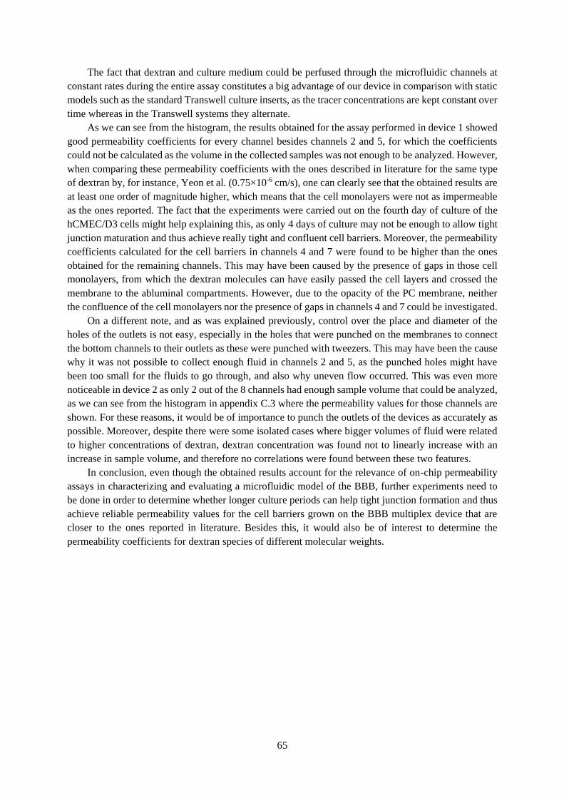
65
The fact that dextran and culture medium could be perfused through the microfluidic channels at
constant rates during the entire assay constitutes a big advantage of our device in comparison with static
models such as the standard Transwell culture inserts, as the tracer concentrations are kept constant over
time whereas in the Transwell systems they alternate.
As we can see from the histogram, the results obtained for the assay performed in device 1 showed
good permeability coefficients for every channel besides channels 2 and 5, for which the coefficients
could not be calculated as the volume in the collected samples was not enough to be analyzed. However,
when comparing these permeability coefficients with the ones described in literature for the same type
of dextran by, for instance, Yeon et al. (0.75×10⁻⁶ cm/s), one can clearly see that the obtained results are
at least one order of magnitude higher, which means that the cell monolayers were not as impermeable
as the ones reported. The fact that the experiments were carried out on the fourth day of culture of the
hCMEC/D3 cells might help explaining this, as only 4 days of culture may not be enough to allow tight
junction maturation and thus achieve really tight and confluent cell barriers. Moreover, the permeability
coefficients calculated for the cell barriers in channels 4 and 7 were found to be higher than the ones
obtained for the remaining channels. This may have been caused by the presence of gaps in those cell
monolayers, from which the dextran molecules can have easily passed the cell layers and crossed the
membrane to the abluminal compartments. However, due to the opacity of the PC membrane, neither
the confluence of the cell monolayers nor the presence of gaps in channels 4 and 7 could be investigated.
On a different note, and as was explained previously, control over the place and diameter of the
holes of the outlets is not easy, especially in the holes that were punched on the membranes to connect
the bottom channels to their outlets as these were punched with tweezers. This may have been the cause
why it was not possible to collect enough fluid in channels 2 and 5, as the punched holes might have
been too small for the fluids to go through, and also why uneven flow occurred. This was even more
noticeable in device 2 as only 2 out of the 8 channels had enough sample volume that could be analyzed,
as we can see from the histogram in appendix C.3 where the permeability values for those channels are
shown. For these reasons, it would be of importance to punch the outlets of the devices as accurately as
possible. Moreover, despite there were some isolated cases where bigger volumes of fluid were related
to higher concentrations of dextran, dextran concentration was found not to linearly increase with an
increase in sample volume, and therefore no correlations were found between these two features.
In conclusion, even though the obtained results account for the relevance of on-chip permeability
assays in characterizing and evaluating a microfluidic model of the BBB, further experiments need to
be done in order to determine whether longer culture periods can help tight junction formation and thus
achieve reliable permeability values for the cell barriers grown on the BBB multiplex device that are
closer to the ones reported in literature. Besides this, it would also be of interest to determine the
permeability coefficients for dextran species of different molecular weights.
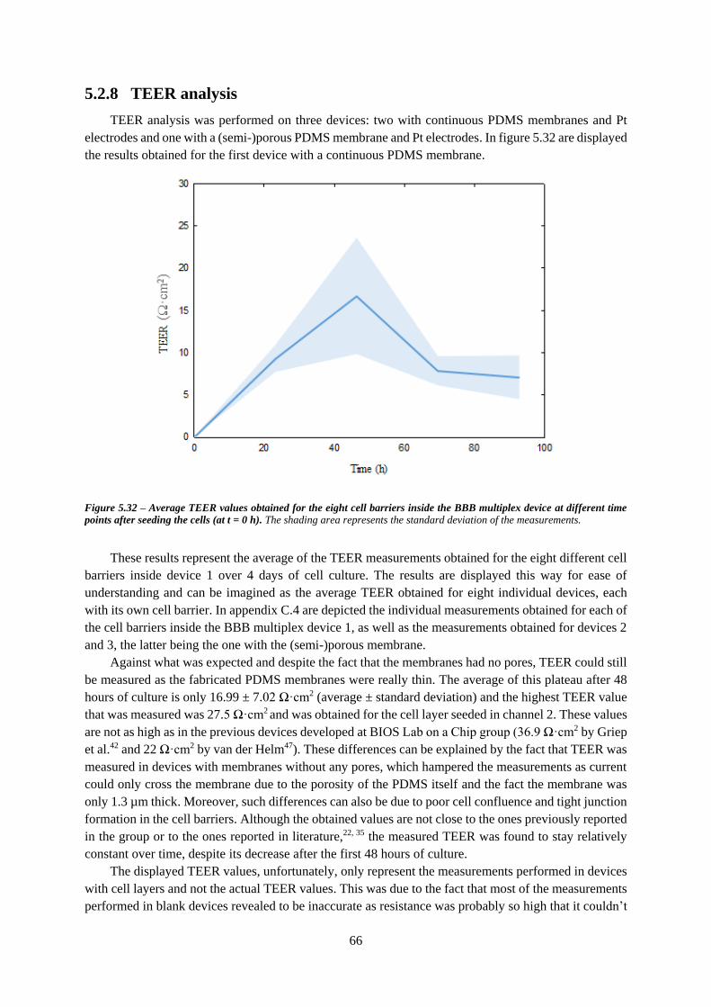
66
5.2.8 TEER analysis
TEER analysis was performed on three devices: two with continuous PDMS membranes and Pt
electrodes and one with a (semi-)porous PDMS membrane and Pt electrodes. In figure 5.32 are displayed
the results obtained for the first device with a continuous PDMS membrane.
These results represent the average of the TEER measurements obtained for the eight different cell
barriers inside device 1 over 4 days of cell culture. The results are displayed this way for ease of
understanding and can be imagined as the average TEER obtained for eight individual devices, each
with its own cell barrier. In appendix C.4 are depicted the individual measurements obtained for each of
the cell barriers inside the BBB multiplex device 1, as well as the measurements obtained for devices 2
and 3, the latter being the one with the (semi-)porous membrane.
Against what was expected and despite the fact that the membranes had no pores, TEER could still
be measured as the fabricated PDMS membranes were really thin. The average of this plateau after 48
hours of culture is only 16.99 ± 7.02 Ω·cm2 (average ± standard deviation) and the highest TEER value
that was measured was 27.5 Ω·cm2 and was obtained for the cell layer seeded in channel 2. These values
are not as high as in the previous devices developed at BIOS Lab on a Chip group (36.9 Ω·cm2 by Griep
et al.42 and 22 Ω·cm2 by van der Helm47). These differences can be explained by the fact that TEER was
measured in devices with membranes without any pores, which hampered the measurements as current
could only cross the membrane due to the porosity of the PDMS itself and the fact the membrane was
only 1.3 µm thick. Moreover, such differences can also be due to poor cell confluence and tight junction
formation in the cell barriers. Although the obtained values are not close to the ones previously reported
in the group or to the ones reported in literature,22, 35 the measured TEER was found to stay relatively
constant over time, despite its decrease after the first 48 hours of culture.
The displayed TEER values, unfortunately, only represent the measurements performed in devices
with cell layers and not the actual TEER values. This was due to the fact that most of the measurements
performed in blank devices revealed to be inaccurate as resistance was probably so high that it couldn’t
Figure 5.32 – Average TEER values obtained for the eight cell barriers inside the BBB multiplex device at different time
points after seeding the cells (at t = 0 h). The shading area represents the standard deviation of the measurements.
67
be measured properly. Another reason why the TEER measured in blank devices might have been
erroneous was due to the fact that sometimes the alligator clamps were not tight enough and if care was
not taken they could disconnect from the wires, thus biasing the measurements. Therefore, such
measurements could not be subtracted from the measurements obtained with cells as in some cases the
final calculated TEER would be negative, which would be impossible. This is shown in figure C.4 in
appendix C, where we can compare the impedance spectra obtained for one channel filled with EGM-2
culture medium and another with hCMEC/D3 cells.
Moreover, looking at the TEER values depicted on tables C.1, C.2 and C.3 in appendix C.4 we can
see that the measurements performed on channels 2 to 7 are higher than the measurements performed
on channels 1 and 8. This can be explained by the overlapping cell layers in the remaining parts of the
microfluidic channels, which are in close contact with the electrodes placed in those channels and
therefore cause the final measured TEER to be increased. This is especially visible for channel 5 of
device 2 and if proven significant, such differences should be corrected with the appropriate
mathematical model, just like it was done for the resistances of the medium-filled channels.
In summary, despite the fact that the obtained TEER values are not as close as we would like to the
ones reported in literature, the possibility to measure TEER in the 2D BBB multiplex system was proven.
However, and unless a more appropriate membrane can be integrated in the device, improvements need
to be done to the PDMS membrane in what concerns pore fabrication so the calculated TEER values are
more accurate and easier to interpret. Furthermore, if a mathematical model that accounts and corrects
for the influence of the overlapping cell layers is developed, not only the obtained TEER values in
devices with PDMS membranes will be more reliable but also devices with integrated PC membranes
could be used to measure the TEER of the cell barriers, as the problem of the electrodes being in contact
with the remaining cell layers would be solved.

68
69
Chapter 6
Conclusion
The main goal of the work described in this report was to develop a multiplexed microfluidic organ-
on-chip platform that could be used for the study of the blood-brain barrier and that allowed the creation
of different experimental conditions at the same time, in the same chip. To achieve this purpose, two
different approaches, a 2D membrane-based and a 3D gel-based, were used.
As detailed in the previous sections, we were able to design and fabricate two different microfluidic
platforms on which several parallel and compartmentalized co-cultures of endothelial and brain cells
can be achieved. In what concerns the two-dimensional model, it fulfilled every requirement drawn in
section 3. Specifically, our device allows the creation of eight different experimental conditions at the
same time without any risk of cross-talk between the different cell layers when pressure at the outlets is
kept similar. This was the main feature of our chip as it enhances the throughput and the reproducibility
of the system and can be of great use in, e.g., the screening of different drugs for treating conditions of
the central nervous system. Moreover, the complexity of the cell barriers can also be evaluated both by
measuring TEER and by performing permeability assays. The influence of fluidic shear on cell growth
and morphology can also be investigated within the platform, as the microfluidic channels can be
continuously perfused just by connecting the device to a pump. Furthermore, due to the dimensions of
the channels, such shear stress was found to be uniform across the channel width.
When validating the devices, we were able to culture equally confluent monolayers of endothelial
cells for at least 5 days. This, along with the results for the distribution of beads and fluorescein within
the device, showed that the design provided an even distribution of the flow and cells with simple
pipetting actions. Experiments where the microfluidic channels of the device were individually
addressed were carried out with dyes, trypsin and ethanol. Mixing between the different solutions only
occurred in the areas where the channels merge together, thus proving the ability of our device in
effectively compartmentalizing the different microenvironments that are created within the chip.
Furthermore, on-chip permeability and TEER analysis yielded promising results. In the case of the
permeability assay, after 4 days of culture the lowest permeability coefficient obtained was 3.6·10-5
cm/s, which was close to the values reported in literature. As for TEER, the highest measured value
(27.5 Ω·cm2) was still far from the ones reported in literature or at the BIOS group. However, the
capability of measuring TEER in our system was well demonstrated. Moreover, with improvements in
the mathematical model used to correct TEER and in the PDMS membranes, especially if through-holes
can be fabricated, the measured TEER is expected to be more accurate and easier to interpret and
compare to other platforms. Therefore, and even though both assays yielded encouraging results, further
experiments need to be done in order to arrive at more reliable values both for the permeability and the
TEER assays. The same should be done to evaluate the influence of shear stress in the cell barriers, as
70
unfortunately these were damaged in every single experiment due to the introduction of air into the
channels.
Another point of improvement was the membrane used in the BBB devices. The opaque PC
membrane was replaced with a clear and transparent one made of PDMS. This membrane not only
improved the monitoring of cells, both with normal phase contrast microscopy and with fluorescence
microscopy, but it also upgraded the fabrication process of two-layer devices. Devices with such
membranes could be fabricated with a simple plasma activation step, thus replacing the long and tedious
gluing process of the membranes in between the PDMS parts and increasing the reproducibility of the
system as the risk of channel clogging due to the introduction of mortar no longer existed. Unfortunately,
the fabrication of through-holes in these membranes could not be optimized and therefore further
research needs to be done in order to arrive at a well-established process. If successful, this would not
only improve the measuring of TEER as it would also allow permeability assays to be performed in
devices with PDMS membranes instead of PC ones, which would enable the monitoring of the diffusion
of the analytes during the entire assay. Furthermore, and when co-culturing endothelial and brain cells,
the PDMS membrane considerably reduces the gap between both PDMS parts created by the 10 µm
thick PC membrane as it is only 1.3 µm thick, which consequently enhances cell-cell interaction.
Besides the 2D model, a 3D device that aimed at more closely mimicking the shape of the human
BBB was also fabricated. In such devices, robust hollow lumens could be created within collagen I and
the hCMEC/D3 cells could be cultured on their inner surfaces, forming three-dimensional shaped cell
layers. However, getting collagen to completely attach to the walls of the devices without the risk of it
collapsing or cells peeling it was not easy and therefore further experimentation is required in order to
find a coating agent for the surfaces of the device that fully prevents this. Regarding the design, despite
the fact that these devices were fabricated only with 3 different compartments, due to the fact that they
are really cost-effective and simple to produce, the number of microfluidic chambers could be easily
increased to any number. Moreover, several experimental conditions can also be generated in these
platforms as the chambers are completely compartmentalized, as was shown in section 5.
In conclusion, the goals set for this work were in a large part successfully met. Not only were we
able to fabricate a microfluidic platform that could be used to study the BBB as it also significantly
increased the throughput of the device used at the BIOS group, without any decrease in the number of
features that can be used to evaluate the integrity of the cell barriers. Furthermore, the fabricated 3D
device also revealed great promise in replacing the conventional flat cell monolayers for ones with a
more three-dimensional nature, thus more closely reproducing the BBB. However, further
experimenting needs to be done in both models in order to arrive at two fully characterized platforms
that can be used by BBB researchers and compared to other data, both in vivo and in vitro.

71
Chapter 7
Recommendations & future perspectives
Although the described microfluidic models were proven to be suitable for various applications,
there are still some questions that need addressing. Regarding the fabrication of the two-dimensional
microfluidic devices, slightly increasing the height of the SU-8 structures on the Si mold to, for instance,
100 µm could be beneficial to help the PDMS membranes not to attach to either the bottom or the top
of the channels. For devices with PC membranes, higher channels would decrease channel clogging
caused by the mortar getting trapped inside of them and would allow the use of a thicker layer of mortar
to glue the PDMS parts, thus reducing the chance of device leakage due to poor bonding of the PC
membrane to PDMS.
Improving the membranes would also be of great importance as our model would benefit greatly if
completely through-holes could be fabricated within the PDMS membranes. Specifically, further
combinations of temperature and curing time of the first layer of positive resist should be tried in order
to find out the optimal one that allows less mixing between the two layers of resist and thus the best
column pattern. Slightly reducing the thickness of the membrane could also be proven helpful as this
would decrease the risk of the pillars being smaller than the thickness of the membrane. This would be
highly advantageous particularly for the on-chip permeability and TEER assays as the diffusion of the
analytes, or compounds, could be monitored and the measured TEER would be more accurate. However,
and in what concerns TEER, such through-holes should only be fabricated in the areas where the top
and bottom channels of the PDMS parts overlap, in order to prevent measuring the TEER of other cell
layers inside the device. To fully characterize the capability of measuring TEER in our platform, it could
also be of interest to evaluate the differences in TEER obtained in devices with membranes without any
pores, with pores everywhere and with pores only in the regions of the channels as this could help
improving the mathematical model used to correct for the geometrical aspects of our platform.
Nevertheless, if obtaining reliable TEER values with the current two-electrode method reveals to be
difficult, different approaches can be tried. Instead of using the Si mold to replicate the chips, chips with
a membrane in between two SU-8 parts with channel openings can be sandwiched between two glass
pieces with sputtered electrodes, which can be made in a variety of metals. As an alternative to the SU-
8 parts, microfluidic channels can also be directly etched in the glass pieces that contain the electrodes
by wet etching. This would not only be useful for measuring TEER as it would also considerably reduce
the fabrication process of devices with integrated electrodes. One drawback of such alternatives,
however, would be the increase in fabrication costs due to the use of SU-8 and glass to make the devices.

72
Another advantageous step would be to investigate the influence of culturing brain cells in the
bottom channels on the overall barrier tightness. This could be quantified by measuring TEER and
performing permeability assays and compared to other data that has been reported in literature so far.
However, robust protocols for the co-culture of different types of cells would need to be designed.
Furthermore, experiments to explore the permeability of the BBB to different drug candidates, for e.g.
Alzheimer’s disease or any other brain conditions, would be of importance.
In addition, the 3D BBB multiplex device could also be improved not only by optimizing the
processes used to fabricate the hollow lumens and to culture the cells within those lumens but also if
micro-needles with smaller diameters were used, in order to arrive at dimensions closer to the ones of
the brain capillaries. Furthermore, with appropriate protocols dynamic cell cultures and permeability
tests could also be carried out to investigate the influence of fluidic shear on the cell barriers and the
permeability of those barriers to certain compounds, respectively. This would be extremely promising
as studying the BBB properties in a device where three-dimensional shaped cell layers that actually
resemble the brain capillaries can be reproduced would be much closer to what happens in vivo.
Moreover, brain cells could also be mixed in the collagen to create a co-culture of endothelial and brain
cells and enhance the physiological relevance of these models.
73
Chapter 8
Bibliography
[1] N. J. Abbott. Prediction of blood-brain barrier permeation in drug discovery from in vivo, in vitro
and in silico models. Drug Discovery Today: Technologies, 1(4), 407–416, 2004.
[2] N. J. Abbott. Dynamics of CNS Barriers: Evolution, Differentiation, and Modulation. Cellular and
Molecular Neurobiology. 25(1), 5-23, 2005.
[3] N. J. Abbott, L. Ronnback, and E. Hansson. Astrocyte-endothelial interactions at the Blood-brain
barrier. Nature Reviews Neuroscience, 7(1), 41–53, 2006.
[4] N. J. Abbott, A. A. K. Patabendige, D. E. M. Dolman, S. R. Yusof, D. J. Begley, Structure and
function of the blood–brain barrier, Neurobiology of Disease, 37(1), 13-25, 2010.
[5] N. J. Abbott. Blood-brain barrier structure and function and the challenges for CNS drug delivery.
Journal of Inherited Metabolic Disease, 36(3), 437–449, 2013.
[6] N. J. Abbott, D. E. M. Dolman, S. R. Yusof, and A. Reichel. In Vitro Models of CNS Barriers.
volume 10 of AAPS Advances in the Pharmaceutical Sciences Series, book section 6, pages 163–197.
Springer New York, 2014.
[7] F. L. Cardoso, D. B., M. A. Brito. Looking at the blood–brain barrier: Molecular anatomy and
possible investigation approaches, Brain Research Reviews, 64(2), 328-363, 2010.
[8] D. J. Begley, M. W. Brightman. Structural and functional aspects of the blood-brain barrier. Progress
in Drug Research, 61, 39-78, 2003.
[9] H. Wolburg, S. Noell, A. Mack, K. Wolburg-Buchholz, P. Fallier-Becker. Brain endothelial cells
and the glio-vascular complex. Cell and Tissue Research, 335(1), 75-96, 2009.
[10] H. Wolburg, A. Lippoldt. Tight junctions of the blood–brain barrier: development, composition
and regulation. Vascular Pharmacology, 38(6), 323-337, 2002.
[11] Y. Chen, L. Liu. Modern methods for delivery of drugs across the blood–brain barrier. Advanced
Drug Delivery Reviews, 64(7), 640-665, 2012.
74
[12] H. Wolburg , K. Wolburg-Buchholz, J. Kraus, G. Rascher-Eggstein, S. Liebner, S. Hamm,
F. Duffner, Ernst-H. Grote, W. Risau, B. Engelhardt. Acta Neuropathologica, 105(6), 586-592, 2003.
[13] R. Booth, H. Kim. Characterization of a microfluidic in vitro model of the blood-brain barrier
(μBBB). Lab on a chip, 12(10), 1784-1792, 2012.
[14] B. T. Hawkins and T. P. Davis. The blood-brain barrier/neurovascular unit in health and disease.
Pharmacological reviews, 57(2), 173-185, 2005.
[15] S. A. Pathan, Z. Iqbal, S. M. Zaidi, S. Talegaonkar, D. Vohra, G. K. Jain, A. Azeem, N. Jain, J. R.
Lalani, R. K. Khar and F. J. Ahmad. CNS drug delivery systems: novel approaches. Recent Patents on
Drug Delivery Formulation, 3(1), 71–89, 2009.
[16] S. Perrin. Make mouse studies work. Nature, 507, 423-425, 2014.
[17] D. Huh, Y.-s. Torisawa, G. A. Hamilton, H. J. Kim, and D. E. Ingber. Microengineered
physiological biomimicry: organs-on-chips. Lab on a chip, 12(12), 2156–2164, 2012.
[18] M. Vastag and G. M. Keseru. Current in vitro and in silico models of blood-brain barrier
penetration: a practical view. Curr Opin Drug Discov Devel, 12(1), 115-124, 2009.
[19] S. Ekins, J. Mestres and B. Testa. In silico pharmacology for drug discovery: applications to targets
and beyond. British journal of pharmacology, 152(1), 21-37, 2007.
[20] A. D. van der Meer and A. van den Berg. Organs-on-chips: breaking the in vitro
impasse. Integrative Biology, 4(5), 2012.
[21] M. W. van der Helm, Blood-Brain Barrier on a microfluidic chip, Master Thesis report at University
of Twente, 2014.
[22] M. W. van der Helm, A. D. van der Meer, J. C. T. Eijkel, A. van den Berg, L. I. Segerink.
Microfluidic organ-on-chip technology for blood-brain barrier research. Tissue Barriers, 4(1), 2016.
[23] T. Korjamo, A. T. Heikkinen, P. Waltari, J. Mönkkönen. The asymmetry of the unstirred water
layer in permeability experiments. Pharm Res, 25(7), 1714-22, 2008.
[24] G. M. Whitesides. The origins and the future of microfluidics. Nature, 4(7101), 368-373, 2006.
[25] A. Manz, D. J. Harrison, E. M. J. Verpoorte, J. C. Fettinger, A. Paulus, H. Lüdi, H. M. Widmer.
Planar chips technology for miniaturization and integration of separation techniques into monitoring
systems: capillary electrophoresis on a chip. Journal of Chromatography A, 593(1), 253-258, 1992.
[26] V. R. Sherman, W. Yang, M. A. Meyers. The materials science of collagen. Journal of the
Mechanical Behavior of Biomedical Materials, 52, 22-50, 2015.
[27] A. Seppänen et al. Distribution of collagen XVII in the human brain. Brain research, 1158, 50-56,
2007.
[28] A. K. H. Achyuta, A. J. Conway, R. B. Crouse, E. C. Bannister, R. N. Lee, C. P. Katnik, A. A.
Behensky, J. Cuevas, and S. S. Sundaram. A modular approach to create a neurovascular unit–on–a–
chip. Lab on a Chip, 13(4), 542–553, 2013.
[29] B. Prabhakarpandian, M. C. Shen, J. B. Nichols, I. R. Mills, M. Sidoryk-Wegrzynowicz, M.
Aschner, and K. Pant. SyM–BBB: a microfluidic blood brain barrier model. Lab on a Chip, 13(6), 1093–
1101, 2013.
75
[30] R. Booth, S. Noh and H. Kim. A multiple-channel, multiple-assay platform for characterization of
full-range shear stress effects on vascular endothelial cells. Lab on a Chip, 14(11), 1880-1890, 2014.
[31] B. Weksler, I. A. Romero, P.-O. Couraud, et al. The hCMEC/D3 cell line as a model of the human
blood-brain barrier. Fluids Barriers CNS, 10(1), 16, 2013.
[32] J. A. Brown JA, V. Pensabene, D. A. Markov, V. Allwardt, M. D. Neely, M. Shi, C. M. Britt, O. S.
Hoilett, Q. Yang, B. M. Brewer, et al. Recreating blood-brain barrier physiology and structure on chip:
A novel neurovascular microfluidic bioreactor. Biomicrofluidics, 9(5), 54-124, 2015.
[33] A. D. Wong, M. Ye, A. F. Levy, J. D. Rothstein, D. E. Bergles, P. C. Searson. The blood-brain
barrier: an engineering perspective. Frontiers in Neuroengineering, 6, 2013.
[34] S. Y. Desai, M. Marroni, L. Cucullo, L. Krizanac-Bengez, M. R. Mayberg, M. T. Hossain, G. G.
Grant, D. Janigro. Mechanisms of endothelial survival under shear stress. Endothelium, 9(2), 89-102,
2002.
[35] Y. Son. Determination of shear viscosity and shear rate from pressure drop and flow rate
relationship in a rectangular channel. Polymer, 48(2), 632–637, 2007.
[36] S. Vanapalli, D. Van den Ende, M. Duits, and F. Mugele. Scaling of interface displacement in a
microfluidic comparator. Applied Physics Letters, 90(11), 114109, 2007.
[37] B. Srinivasan, A. R. Kolli, M. B. Esch, H. E. Abaci, M. L. Shuler and J. J. Hickman. TEER
Measurement Techniques for In Vitro Barrier Model Systems. Journal of Laboratory Automation, 20(2),
107-126, 2015.
[38] K. Benson, S. Cramer and H. J. Galla. Impedance-based cell monitoring: barrier properties and
beyond. Fluids Barriers CNS, 10(1), 5, 2013.
[39] N. J. Douville, Y. C. Tung, R. Li et al. Fabrication of Two-Layered Channel System with Embedded
Electrodes to Measure Resistance across Epithelial and Endothelial Barriers. Analytical Chemistry.
82(6), 2505–2511, 2010.
[40] Bjorn de Wagenaar, Blood-Brain Barrier on a chip, Master Thesis report at University of Twente,
2011.
[41] J. H. Yeon, D. Na, K. Choi, S.W. Ryu, C. Choi, and J. K. Park. Reliable permeability assay system
in a microfluidic device mimicking cerebral vasculatures. Biomedical Microdevices, 14(6), 1141–1148,
2012.
[42] L. M. Griep, F. Wolbers, B. de Wagenaar, P. M. ter Braak, B. B. Weksler, I. A. Romero, P. O.
Couraud, I. Vermes, A. D. van der Meer, and A. van den Berg. BBB ON CHIP: microfluidic platform
to mechanically and biochemically modulate blood–brain barrier function. Biomedical Microdevices,
15(1), 145–150, 2013.
[43] H. Cho, J. H. Seo, K. H. Wong, Y. Terasaki, J. Park, K. Bong, K. Arai, E. H. Lo, D. Irimia. Three-
Dimensional Blood-Brain Barrier Model for in vitro Studies of Neurovascular Pathology. Scientific
reports, 5, 15222, 2015.
[44] J. A. Kim, H. N. Kim, S-K Im, S. Chung, J. Y. Kang, N. Choi. Collagen-based brain
microvasculature model in vitro using three-dimensional printed template. Biomicrofluidics, 9(2),
24115, 2015.
76
[45] K. L. Sellgren, B. T. Hawkins, S. Grego. An optically transparent membrane supports shear stress
studies in a three-dimensional microfluidic neurovascular unit model. Biomicrofluidics, 9(6), 61-102,
2015.
[46] F. R. Walter, S. Valkai, A. Kincses, A. Petneházi, T. Czeller, S. Veszelka, P. Ormos, M. A. Deli
and A. Dér. A versatile lab-on-a-chip tool for modeling biological barriers. Sensors and Actuators B:
Chemical, 222, 1209-19, 2016.
[47] M. W. van der Helm, M. Odijk, J-P. Frimat, A. D. van der Meer, J. C. T. Eijkel, A. van der Berg,
L. I. Segerink. Direct quantification of transendothelial electrical resistance in organs-on-
chips. Biosensors and Bioelectronics, 85, 924-929, 2016.
[48] J. R. Anderson, D. T. Chiu, R. J. Jackman, O. Cherniavskaya, J. C. McDonald, H. Wu, S. H.
Whitesides, G. M. Whitesides. Fabrication of topologically complex three-dimensional microfluidic
systems in PDMS by rapid prototyping. Analytical Chemistry, 72(14), 3158-3164, 2000.
[49] Cecil D. Murray. The Physiological Principle of Minimum Work: I. The Vascular System and the
Cost of Blood Volume. Proceedings of the National Academy of Sciences of the United States of
America, 12(3), 207–214, 1926.
[50] Cecil D. Murray. The Physiological Principle of Minimum Work: II. Oxygen Exchange in
Capillaries. Proceedings of the National Academy of Sciences of the United States of America, 12(5),
299–304, 1926.
[51] Baskin Engineering UC Santa Cruz. Nano-and Microscale Fabrication and Characterization.
http://cleanroom.soe.ucsc.edu/microfluidics. Assessed in November 2016.
[52] D. Huh, H. J. Kim, J. P. Fraser, D. E. Shea, M. Khan, A. Bahinski, G. A. Hamilton, D. E. Ingber.
Microfabrication of human organs-on-chips. Nature Protocols, 8(11), 2135-2157, 2013.
[53] E. Kang, J. Ryoo, G. S. Jeong, Y. Y. Choi, S. M. Jeong, J. Ju, S. Chung, S. Takayama, S-H. Lee.
Large-scale, Ultrapliable, and Free-standing Nanomembranes. Advanced Materials, 25(15), 2167-2173,
2013.
[54] B.-h. Chueh, D. Huh, C. R. Kyrtsos, T. Houssin, N. Futai, and S. Takayama. Leakage-free bonding
of porous membranes into layered microfluidic array systems. Analytical Chemistry, 79(9), 3504–3508,
2007.
[55] P. A. Vogel, S. T. Halpin, R. S. Martin, and D. M. Spence. Microfluidic transendothelial electrical
resistance measurement device that enables blood flow and postgrowth experiments. Analytical
Chemistry, 83(11), 4296–4301, 2011.
[56] B. B. Weksler, E. A. Subileau, N. Perriere, P. Charneau, K. Holloway, M. Leveque, H. Tricoire-
Leignel, A. Nicotra, S. Bourdoulous, and P. Turowski. Blood–brain barrier–specific properties of a
human adult brain endothelial cell line. The FASEB Journal, 19(13), 1872–1874, 2005.
[57] M. Odijk, A. D. van der Meer, D. Levner, H. J. Kim, M. W. van der Helm, L. I Segerink, J-P.
Frimat, G. A. Hamilton, D. E. Ingber, A. van den Berg. Measuring direct current trans-epithelial
electrical resistance in organ-on-a-chip microsystems. Lab on a Chip, 15, 745-52, 2015.
[58] W. M. Pardridge. Drug transport across the blood–brain barrier. Journal of Cerebral Blood Flow
& Metabolism, 32(11), 1959-1972, 2012.

77
[59] R. Thuenauer, E. Rodriguez-Boulan, and W. Römer. Microfluidic approaches for epithelial cell
layer culture and characterisation. Analyst, 139(13), 3206-3218, 2014.
[60] C. Zang, Z. Zhao, N. A. Rahim, D. Noort and H. Yu. Towards a human-on-chip: culturing multiple
cell types on a chip with compartmentalized microenvironments. Lab on a Chip, 9(22), 3185-3192,
2009.
[61] G. Shao, J. Wang, Z. Li, L. Saraf, W. Wang and Y. Lin. Poly (dimethylsiloxane) microchip-based
immunoassay with multiple reaction zones: Toward on-chip multiplex detection platform. Sensors and
Actuators B: Chemical, 159(1), 44-50, 2011.
[62] N. Wongkaew, P. He, V. Kurth, W. Surareungchai and A. J. Baeumner. Multi-channel PMMA
microfluidic biosensor with integrated IDUAs for electrochemical detection. Analytical and
Bioanalytical Chemistry, 405(18), 5965-5974, 2013.

78

79
Appendices

80

81
Appendix A
Conference submission
On the next pages the paper that was accepted at the MicroNanoConference 2016 and the corresponding
poster are presented. This conference aims at bringing together the active involvement of industry,
science and user community of microsystems and nanotechnology, spanning basic research, engineering
science, technology, equipment and instrumentation.1
1 MicroNano Conference organization. International MicroNano Conference Amsterdam 2016. http://
www.micronanoconference.org
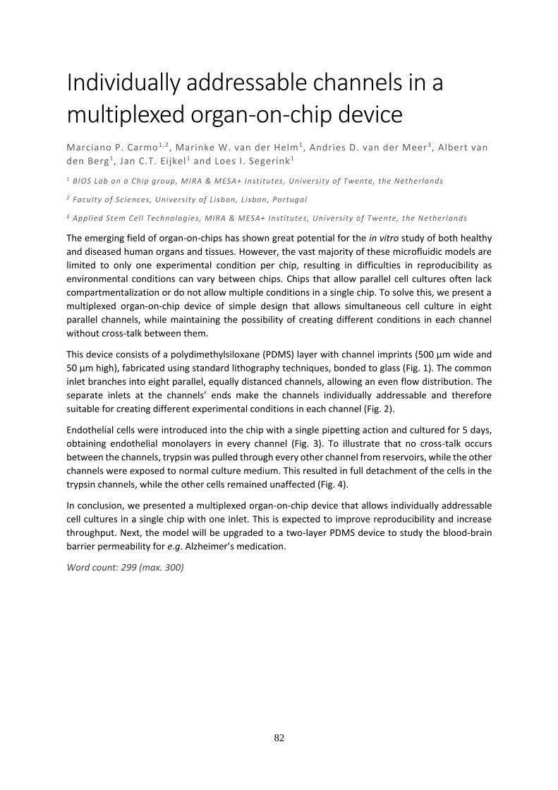
82
Individually addressable channels in a multiplexed organ-on-chip device Marciano P. Carmo1,2, Marinke W. van der Helm 1, Andries D. van der Meer3, Albert van
den Berg1, Jan C.T. Eijkel1 and Loes I. Segerink1
1 BIOS Lab on a Chip group, MIRA & MESA+ Institutes, University of Twente, the Netherlands
2 Faculty of Sciences, University of Lisbon, Lisbon, Portugal
3 Applied Stem Cell Technologies, MIRA & MESA+ Institutes, University of Twente, the Netherlands
The emerging field of organ-on-chips has shown great potential for the in vitro study of both healthy
and diseased human organs and tissues. However, the vast majority of these microfluidic models are
limited to only one experimental condition per chip, resulting in difficulties in reproducibility as
environmental conditions can vary between chips. Chips that allow parallel cell cultures often lack
compartmentalization or do not allow multiple conditions in a single chip. To solve this, we present a
multiplexed organ-on-chip device of simple design that allows simultaneous cell culture in eight
parallel channels, while maintaining the possibility of creating different conditions in each channel
without cross-talk between them.
This device consists of a polydimethylsiloxane (PDMS) layer with channel imprints (500 µm wide and
50 µm high), fabricated using standard lithography techniques, bonded to glass (Fig. 1). The common
inlet branches into eight parallel, equally distanced channels, allowing an even flow distribution. The
separate inlets at the channels’ ends make the channels individually addressable and therefore
suitable for creating different experimental conditions in each channel (Fig. 2).
Endothelial cells were introduced into the chip with a single pipetting action and cultured for 5 days,
obtaining endothelial monolayers in every channel (Fig. 3). To illustrate that no cross-talk occurs
between the channels, trypsin was pulled through every other channel from reservoirs, while the other
channels were exposed to normal culture medium. This resulted in full detachment of the cells in the
trypsin channels, while the other cells remained unaffected (Fig. 4).
In conclusion, we presented a multiplexed organ-on-chip device that allows individually addressable
cell cultures in a single chip with one inlet. This is expected to improve reproducibility and increase
throughput. Next, the model will be upgraded to a two-layer PDMS device to study the blood-brain
barrier permeability for e.g. Alzheimer’s medication.
Word count: 299 (max. 300)
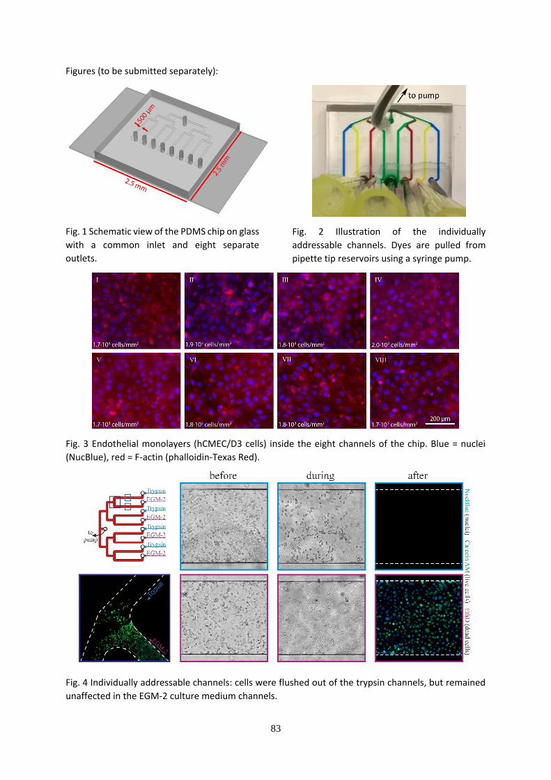
83
Figures (to be submitted separately):
Fig. 1 Schematic view of the PDMS chip on glass
with a common inlet and eight separate
outlets.
Fig. 2 Illustration of the individually
addressable channels. Dyes are pulled from
pipette tip reservoirs using a syringe pump.
Fig. 3 Endothelial monolayers (hCMEC/D3 cells) inside the eight channels of the chip. Blue = nuclei
(NucBlue), red = F-actin (phalloidin-Texas Red).
Fig. 4 Individually addressable channels: cells were flushed out of the trypsin channels, but remained
unaffected in the EGM-2 culture medium channels.
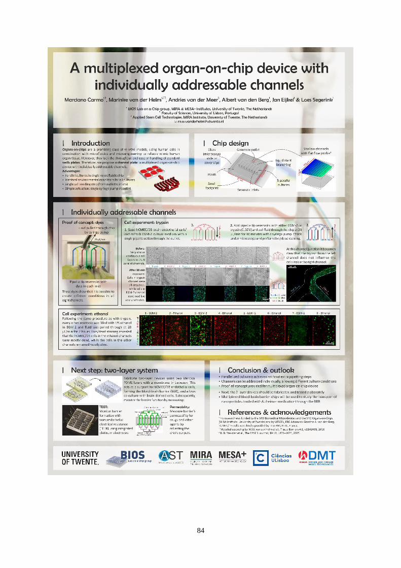
84
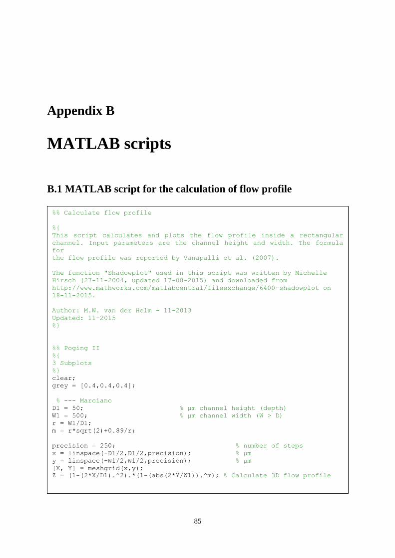
85
Appendix B
MATLAB scripts
B.1 MATLAB script for the calculation of flow profile
%% Calculate flow profile
%
This script calculates and plots the flow profile inside a rectangular
channel. Input parameters are the channel height and width. The formula
for
the flow profile was reported by Vanapalli et al. (2007).
The function "Shadowplot" used in this script was written by Michelle
Hirsch (27-11-2004, updated 17-08-2015) and downloaded from
http://www.mathworks.com/matlabcentral/fileexchange/6400-shadowplot on
18-11-2015.
Author: M.W. van der Helm - 11-2013
Updated: 11-2015
%
%% Poging II
%
3 Subplots
%
clear;
grey = [0.4,0.4,0.4];
% --- Marciano
D1 = 50; % µm channel height (depth)
W1 = 500; % µm channel width (W > D)
r = W1/D1;
m = r*sqrt(2)+0.89/r;
precision = 250; % number of steps
x = linspace(-D1/2,D1/2,precision); % µm
y = linspace(-W1/2,W1/2,precision); % µm
[X, Y] = meshgrid(x,y);
Z = (1-(2*X/D1).^2).*(1-(abs(2*Y/W1)).^m); % Calculate 3D flow profile
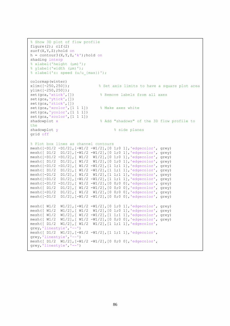
86
% Show 3D plot of flow profile
figure(2); clf(2)
surf(X,Y,Z);hold on
h = contour3(X,Y,Z,'k');hold on
shading interp
% xlabel('height (µm)');
% ylabel('width (µm)');
% zlabel('z: speed (u/u_max)');
colormap(winter)
xlim([-250,250]); % Set axis limits to have a square plot area
ylim([-250,250]);
set(gca,'xtick',[]) % Remove labels from all axes
set(gca,'ytick',[])
set(gca,'ztick',[]) set(gca,'xcolor',[1 1 1]) % Make axes white set(gca,'ycolor',[1 1 1]) set(gca,'zcolor',[1 1 1]) shadowplot x % Add "shadows" of the 3D flow profile to
the shadowplot y % side planes grid off
% Plot box lines as channel contours mesh([-D1/2 -D1/2],[-W1/2 -W1/2],[0 1;0 1],'edgecolor', grey) mesh([ D1/2 D1/2],[-W1/2 -W1/2],[0 1;0 1],'edgecolor', grey) mesh([-D1/2 -D1/2],[ W1/2 W1/2],[0 1;0 1],'edgecolor', grey) mesh([ D1/2 D1/2],[ W1/2 W1/2],[0 1;0 1],'edgecolor', grey) mesh([-D1/2 -D1/2],[ W1/2 -W1/2],[1 1;1 1],'edgecolor', grey) mesh([ D1/2 D1/2],[ W1/2 -W1/2],[1 1;1 1],'edgecolor', grey) mesh([-D1/2 D1/2],[ W1/2 W1/2],[1 1;1 1],'edgecolor', grey) mesh([-D1/2 D1/2],[-W1/2 -W1/2],[1 1;1 1],'edgecolor', grey) mesh([-D1/2 -D1/2],[ W1/2 -W1/2],[0 0;0 0],'edgecolor', grey) mesh([ D1/2 D1/2],[ W1/2 -W1/2],[0 0;0 0],'edgecolor', grey) mesh([-D1/2 D1/2],[ W1/2 W1/2],[0 0;0 0],'edgecolor', grey) mesh([-D1/2 D1/2],[-W1/2 -W1/2],[0 0;0 0],'edgecolor', grey)
mesh([ W1/2 W1/2],[-W1/2 -W1/2],[0 1;0 1],'edgecolor', grey) mesh([ W1/2 W1/2],[ W1/2 W1/2],[0 1;0 1],'edgecolor', grey) mesh([ W1/2 W1/2],[ W1/2 -W1/2],[1 1;1 1],'edgecolor', grey) mesh([ W1/2 W1/2],[ W1/2 -W1/2],[0 0;0 0],'edgecolor', grey) mesh([ D1/2 W1/2],[ W1/2 W1/2],[1 1;1 1],'edgecolor',
grey,'linestyle','--') mesh([ D1/2 W1/2],[-W1/2 -W1/2],[1 1;1 1],'edgecolor',
grey,'linestyle','--') mesh([ D1/2 W1/2],[-W1/2 -W1/2],[0 0;0 0],'edgecolor',
grey,'linestyle','--')
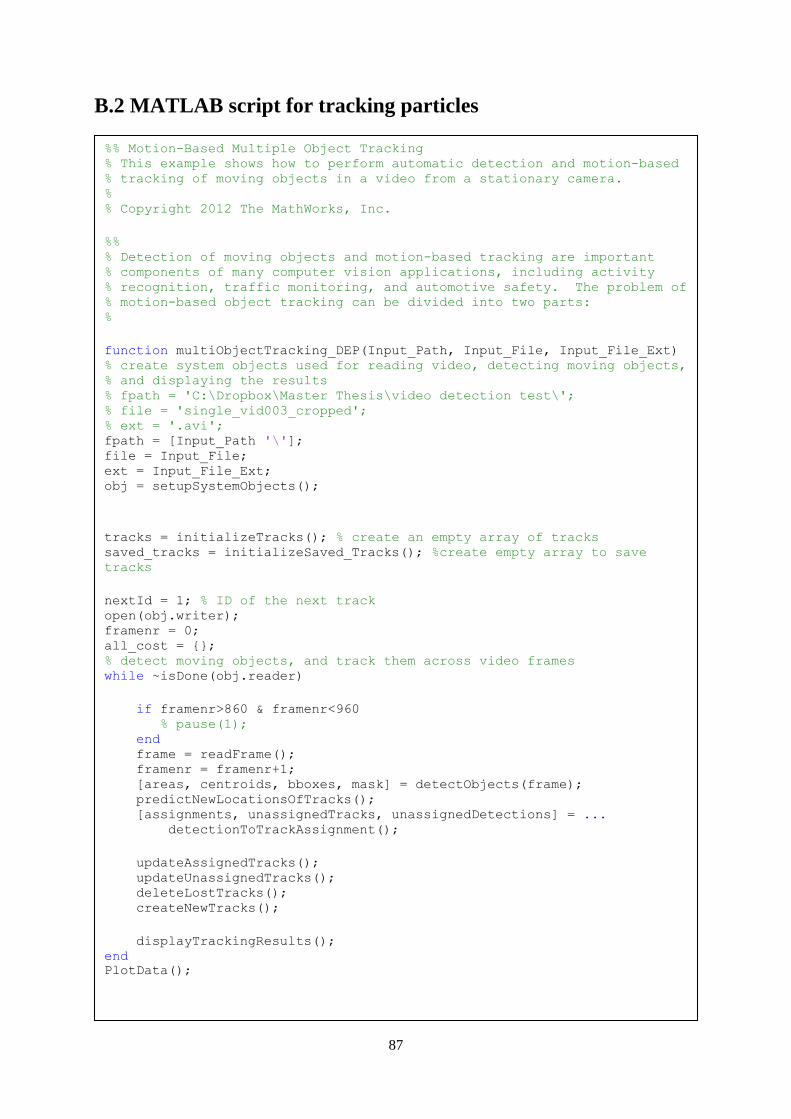
87
B.2 MATLAB script for tracking particles
%% Motion-Based Multiple Object Tracking % This example shows how to perform automatic detection and motion-based % tracking of moving objects in a video from a stationary camera. % % Copyright 2012 The MathWorks, Inc.
%% % Detection of moving objects and motion-based tracking are important % components of many computer vision applications, including activity % recognition, traffic monitoring, and automotive safety. The problem of % motion-based object tracking can be divided into two parts: %
function multiObjectTracking_DEP(Input_Path, Input_File, Input_File_Ext) % create system objects used for reading video, detecting moving objects, % and displaying the results % fpath = 'C:\Dropbox\Master Thesis\video detection test\'; % file = 'single_vid003_cropped'; % ext = '.avi'; fpath = [Input_Path '\']; file = Input_File; ext = Input_File_Ext; obj = setupSystemObjects();
tracks = initializeTracks(); % create an empty array of tracks saved_tracks = initializeSaved_Tracks(); %create empty array to save
tracks
nextId = 1; % ID of the next track open(obj.writer); framenr = 0; all_cost = ; % detect moving objects, and track them across video frames while ~isDone(obj.reader)
if framenr>860 & framenr<960 % pause(1); end frame = readFrame(); framenr = framenr+1; [areas, centroids, bboxes, mask] = detectObjects(frame); predictNewLocationsOfTracks(); [assignments, unassignedTracks, unassignedDetections] = ... detectionToTrackAssignment();
updateAssignedTracks(); updateUnassignedTracks(); deleteLostTracks(); createNewTracks();
displayTrackingResults(); end PlotData();

88
%% Create System Objects % Create System objects used for reading the video frames, detecting % foreground objects, and displaying results.
function obj = setupSystemObjects() % Initialize Video I/O % Create objects for reading a video from a file, drawing the
tracked % objects in each frame, and playing the video.
% create a video file reader obj.reader = vision.VideoFileReader([fpath file ext]);
%FPS hieruit toveren vidHeight = obj.reader.info.VideoSize(2); vidWidth = obj.reader.info.VideoSize(1); obj.writer = VideoWriter([fpath 'Object_Tracked' file
ext],'Uncompressed AVI'); obj.writer.FrameRate=obj.reader.info.VideoFrameRate;
% create two video players, one to display the video, % and one to display the foreground mask obj.videoPlayer = vision.VideoPlayer('Position',[10 50
50+vidWidth 50+vidHeight]); obj.maskPlayer = vision.VideoPlayer('Position',[10
50+50+vidHeight 50+vidWidth 50+vidHeight]);
% Create system objects for foreground detection and blob
analysis
% The foreground detector is used to segment moving objects from % the background. It outputs a binary mask, where the pixel value % of 1 corresponds to the foreground and the value of 0
corresponds % to the background.
obj.detector = vision.ForegroundDetector( 'AdaptLearningRate',
1 , ... 'NumTrainingFrames', 40, ... 'LearningRate', 0.00005,
...'MinimumBackgroundRatio', 0.95 , .... 'NumGaussians', 5, ...
'InitialVariance' , (70/255)^2 ...); % Connected groups of foreground pixels are likely to correspond
to moving % objects. The blob analysis system object is used to find such
groups % (called 'blobs' or 'connected components'), and compute their % characteristics, such as area, centroid, and the bounding box.
obj.blobAnalyser = vision.BlobAnalysis('BoundingBoxOutputPort',
true, ... 'AreaOutputPort', true, 'CentroidOutputPort', true, ... 'MinimumBlobArea', 1); end

89
%% Initialize Tracks % The |initializeTracks| function creates an array of tracks, where each % track is a structure representing a moving object in the video. The % purpose of the structure is to maintain the state of a tracked object. % The state consists of information used for detection to track
assignment, track termination, and display. function tracks = initializeTracks() % create an empty array of tracks tracks = struct(... 'id', , ... 'bbox', , ... 'kalmanFilter', , ... 'age', , ... 'totalVisibleCount', , ... 'consecutiveInvisibleCount', ); end %% Initialize Tracks % The |initializeSaved Tracks| function creates an array of tracks, where % the location points of the track are saved corresponding to the frame % number. function saved_tracks = initializeSaved_Tracks() % create an empty array of saved_tracks saved_tracks = struct(...'id',struct( 'frame', [], ...
'measured_centroid', [], ... 'time',[] ...)...); end %% Read a Video Frame % Read the next video frame from the video file. function frame = readFrame() frame = obj.reader.step(); end %% Detect Objects % The |detectObjects| function returns the centroids and the bounding
boxes % of the detected objects. It also returns the binary mask, which has the % same size as the input frame. Pixels with a value of 1 correspond to
the % foreground, and pixels with a value of 0 correspond to the background. function [areas, centroids, bboxes, mask] = detectObjects(frame) % detect foreground mask = obj.detector.step(frame); % apply morphological operations to remove noise and fill in holes mask = imopen(mask, strel('line', 2, -1)); %mask = bwmorph(mask,'bridge'); mask = imclose(mask, strel('line', 2, -1)); %mask = imfill(mask, 'holes'); mask = bwareaopen(mask,1,1); % perform blob analysis to find connected components [areas, centroids, bboxes] = obj.blobAnalyser.step(mask); if size(bboxes,1)>0 bboxes(:,1:2) = centroids; bboxes(:,3) = 5; bboxes(:,4) = 5; end end
90
%% Predict New Locations of Existing Tracks % Use the Kalman filter to predict the centroid of each track in the % current frame, and update its bounding box accordingly.
function predictNewLocationsOfTracks() for i = 1:length(tracks) bbox = tracks(i).bbox;
% predict the current location of the track predictedCentroid = predict(tracks(i).kalmanFilter);
% shift the bounding box so that its center is at % the predicted location predictedCentroid = int32(predictedCentroid) - bbox(3:4) / 2; tracks(i).bbox = [predictedCentroid, bbox(3:4)];
end end
%% Assign Detections to Tracks % Assigning object detections in the current frame to existing tracks is % done by minimizing cost. The cost is defined as the negative % log-likelihood of a detection corresponding to a track. % function [assignments, unassignedTracks, unassignedDetections] = ... detectionToTrackAssignment()
nTracks = length(tracks); nDetections = size(centroids, 1);
% compute the cost of assigning each detection to each track cost = zeros(nTracks, nDetections); for i = 1:nTracks cost(i, :) = distance(tracks(i).kalmanFilter, centroids); end
all_cost(end +1) = cost; % solve the assignment problem costOfNonAssignment = 15; [assignments, unassignedTracks, unassignedDetections] = ... assignDetectionsToTracks(cost, costOfNonAssignment); end %% Update Assigned Tracks % The |updateAssignedTracks| function updates each assigned track with
the % corresponding detection. It calls the |correct| method of % |vision.KalmanFilter| to correct the location estimate. Next, it stores % the new bounding box, and increases the age of the track and the total % visible count by 1. Finally, the function sets the invisible count to
0.
91
function updateAssignedTracks() numAssignedTracks = size(assignments, 1); for i = 1:numAssignedTracks trackIdx = assignments(i, 1); detectionIdx = assignments(i, 2); centroid = centroids(detectionIdx, :); bbox = bboxes(detectionIdx, :); area = areas(detectionIdx, :); %save track data id=tracks(trackIdx).id; if size(saved_tracks.id,2)>=id frameind = size(saved_tracks.id(id).frame,1); else frameind = 0; end; saved_tracks.id(id).frame(frameind+1,:) = framenr; saved_tracks.id(id).time(frameind+1,:) =
saved_tracks.id(id).frame(frameind+1,:)/25; saved_tracks.id(id).measured_centroid(frameind+1,:) =
centroid; saved_tracks.id(id).area(frameind+1,:) = area;
% saved_tracks.id(1,1).frame(end)-
saved_tracks.id(1,1).frame(1)/25; % Correct the estimate of the object's location % using the new detection. correct(tracks(trackIdx).kalmanFilter, centroid);
% replace predicted bounding box with detected % bounding box tracks(trackIdx).bbox = bbox;
% update track's age tracks(trackIdx).age = tracks(trackIdx).age + 1;
% update visibility tracks(trackIdx).totalVisibleCount = ... tracks(trackIdx).totalVisibleCount + 1; tracks(trackIdx).consecutiveInvisibleCount = 0; end end
%% Update Unassigned Tracks % Mark each unassigned track as invisible, and increase its age by 1.
function updateUnassignedTracks() for i = 1:length(unassignedTracks) ind = unassignedTracks(i); tracks(ind).age = tracks(ind).age + 1; tracks(ind).consecutiveInvisibleCount = ... tracks(ind).consecutiveInvisibleCount + 1; end end
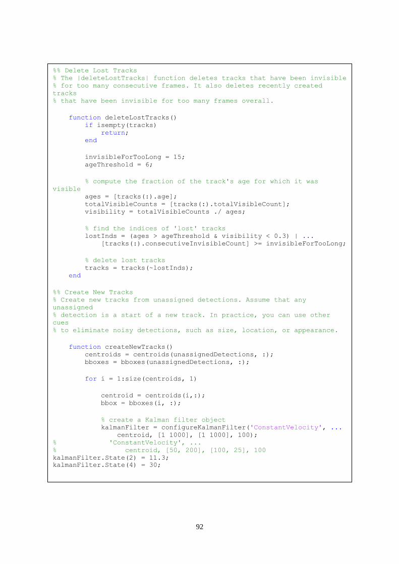
92
%% Delete Lost Tracks % The |deleteLostTracks| function deletes tracks that have been invisible % for too many consecutive frames. It also deletes recently created
tracks % that have been invisible for too many frames overall.
function deleteLostTracks() if isempty(tracks) return; end
invisibleForTooLong = 15; ageThreshold = 6;
% compute the fraction of the track's age for which it was
visible ages = [tracks(:).age]; totalVisibleCounts = [tracks(:).totalVisibleCount]; visibility = totalVisibleCounts ./ ages;
% find the indices of 'lost' tracks lostInds = (ages > ageThreshold & visibility < 0.3) | ... [tracks(:).consecutiveInvisibleCount] >= invisibleForTooLong;
% delete lost tracks tracks = tracks(~lostInds); end
%% Create New Tracks % Create new tracks from unassigned detections. Assume that any
unassigned % detection is a start of a new track. In practice, you can use other
cues % to eliminate noisy detections, such as size, location, or appearance.
function createNewTracks() centroids = centroids(unassignedDetections, :); bboxes = bboxes(unassignedDetections, :);
for i = 1:size(centroids, 1)
centroid = centroids(i,:); bbox = bboxes(i, :);
% create a Kalman filter object kalmanFilter = configureKalmanFilter('ConstantVelocity', ... centroid, [1 1000], [1 1000], 100); % 'ConstantVelocity', ... % centroid, [50, 200], [100, 25], 100 kalmanFilter.State(2) = 11.3;
kalmanFilter.State(4) = 30;
93
% create a new track newTrack = struct(... 'id', nextId, ... 'bbox', bbox, ... 'kalmanFilter', kalmanFilter, ... 'age', 1, ... 'totalVisibleCount', 1, ... 'consecutiveInvisibleCount', 0);
% add it to the array of tracks tracks(end + 1) = newTrack;
% increment the next id nextId = nextId + 1; end end
%% Display Tracking Results % The |displayTrackingResults| function draws a bounding box and label ID % for each track on the video frame and the foreground mask. It then % displays the frame and the mask in their respective video players.
function displayTrackingResults() % convert the frame and the mask to uint8 RGB frame = im2uint8(frame); mask = uint8(repmat(mask, [1, 1, 3])) .* 255;
minVisibleCount = 1; if ~isempty(tracks) reliableTrackInds = ... [tracks(:).totalVisibleCount] > minVisibleCount; reliableTracks = tracks(reliableTrackInds);
% display the objects. If an object has not been detected % in this frame, display its predicted bounding box. if ~isempty(reliableTracks) % get bounding boxes bboxes = cat(1, reliableTracks.bbox); % get ids ids = int32([reliableTracks(:).id]);
% create labels for objects indicating the ones for % which we display the predicted rather than the actual % location labels = cellstr(int2str(ids')); predictedTrackInds = ... [reliableTracks(:).consecutiveInvisibleCount] > 0; isPredicted = cell(size(labels)); isPredicted(predictedTrackInds) = ' predicted'; labels = strcat(labels, isPredicted);
94
% draw on the frame frame = insertObjectAnnotation(frame, 'circle', ... bboxes(:,1:3), labels);
% draw on the mask mask = insertObjectAnnotation(mask, 'circle', ... bboxes(:,1:3), labels); end end
% display the mask and the frame obj.maskPlayer.step(mask); obj.videoPlayer.step(frame); writeVideo(obj.writer,frame); end
close(obj.writer);
function PlotData() save([fpath file 'saved_tracks.mat'],'saved_tracks'); end end
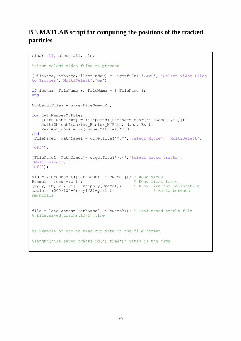
95
B.3 MATLAB script for computing the positions of the tracked
particles
clear all, close all, clc;
%First select video files to procces
[FileName,PathName,FilterIndex] = uigetfile('*.avi', 'Select Video Files
to Procces','MultiSelect','on');
if ischar( FileName ), FileName = FileName ; end
NumberOfFiles = size(FileName,2);
for i=1:NumberOfFiles [Path Name Ext] = fileparts([PathName char(FileName(1,i))]); multiObjectTracking_Basler_M(Path, Name, Ext); Percent_done = i/(NumberOfFiles)*100 end [FileName1, PathName1]= uigetfile('*.*','Select Movie', 'MultiSelect',
... 'off');
[FileName2, PathName2]= uigetfile('*.*','Select saved tracks',
'MultiSelect', ... 'off');
vid = VideoReader([PathName1 FileName1]); % Read video Frame1 = read(vid,1); % Read first frame [x, y, BW, xi, yi] = roipoly(Frame1); % Draw line for calibration ratio = (500*10^-6)/(yi(2)-yi(1)); % Ratio between
µm/pixels
file = load(strcat(PathName2,FileName2)); % Load saved tracks file % file.saved_tracks.id(5).time ;
%% Example of how to read out data in the file format
%length(file.saved_tracks.id(j).time'); %this is the time
96
B.4 MATLAB script for calculating the velocities of the tracked
particles from the saved tracks
close all; clc; %% Definition of parameters and empty matrices time=10; %time in seconds nframes=2000; %number of frames dt=time/nframes; %timestep
n=length(file.saved_tracks.id);
t=zeros(n,nframes); f=zeros(n,nframes); p1=zeros(n,nframes); p2=zeros(n,nframes); NumberOfNonPaddedEntries=zeros(n,1);
vx=zeros(n,nframes); vy=zeros(n,nframes);
%% Filling of time, frame and centroid information j=1;
for j=1:(n) u=length(file.saved_tracks.id(j).time'); NumberOfNonPaddedEntries(j)=u; if u==0 j=j+1; else t(j,:)=padarray(file.saved_tracks.id(j).time',[0 nframes-
length(file.saved_tracks.id(j).time')],'post'); f(j,:)=padarray(file.saved_tracks.id(j).frame',[0 nframes-
length(file.saved_tracks.id(j).frame')],'post'); p1(j,:)=padarray(file.saved_tracks.id(j).measured_centroid(:,1)',[0
nframes-length(file.saved_tracks.id(j).measured_centroid(:,1)')],'post'); p2(j,:)=padarray(file.saved_tracks.id(j).measured_centroid(:,2)',[0
nframes-length(file.saved_tracks.id(j).measured_centroid(:,2)')],'post'); j=j+1; end end
%% Calculation of the velocity i=1; j=1; for j=1:n for i=1:(NumberOfNonPaddedEntries-1) vx(j,i)=ratio*(p1(j,i+1)-p1(j,i))/dt'; vy(j,i)=ratio*(p2(j,i+1)-p2(j,i))/dt'; i=i+1; end j=j+1; end
%% Plot velocities j=1; figure(1) hold on for j=1:n
plot(1:1:NumberOfNonPaddedEntries(j),vx(j,1:NumberOfNonPaddedEntries(j))) j=j+1; end hold off
j=1;
97
%% Plot velocities j=1; figure(1) hold on for j=1:n
plot(1:1:NumberOfNonPaddedEntries(j),vx(j,1:NumberOfNonPaddedEntries(j))) j=j+1; end hold off
j=1; figure(2) hold on for j=1:n
plot(1:1:NumberOfNonPaddedEntries(j),vy(j,1:NumberOfNonPaddedEntries(j))) j=j+1; end hold off
%% Calculate averages
%velocity_x j=1; for j=1:n if NumberOfNonPaddedEntries(j)==0 Average_vx(j)=NaN; j=j+1; else Average_vx(j)=mean(vx(j,1:NumberOfNonPaddedEntries(j))); j=j+1; end end Average_vx(find(isnan(Average_vx))) = []; Average19=mean(Average_vx)
for j=1:n if NumberOfNonPaddedEntries(j)==0 Average_vy(j)=NaN; j=j+1; else Average_vy(j)=mean(vy(j,1:NumberOfNonPaddedEntries(j))); j=j+1; end end Average_vy(find(isnan(Average_vy))) = []; Average20=mean(Average_vy)

98
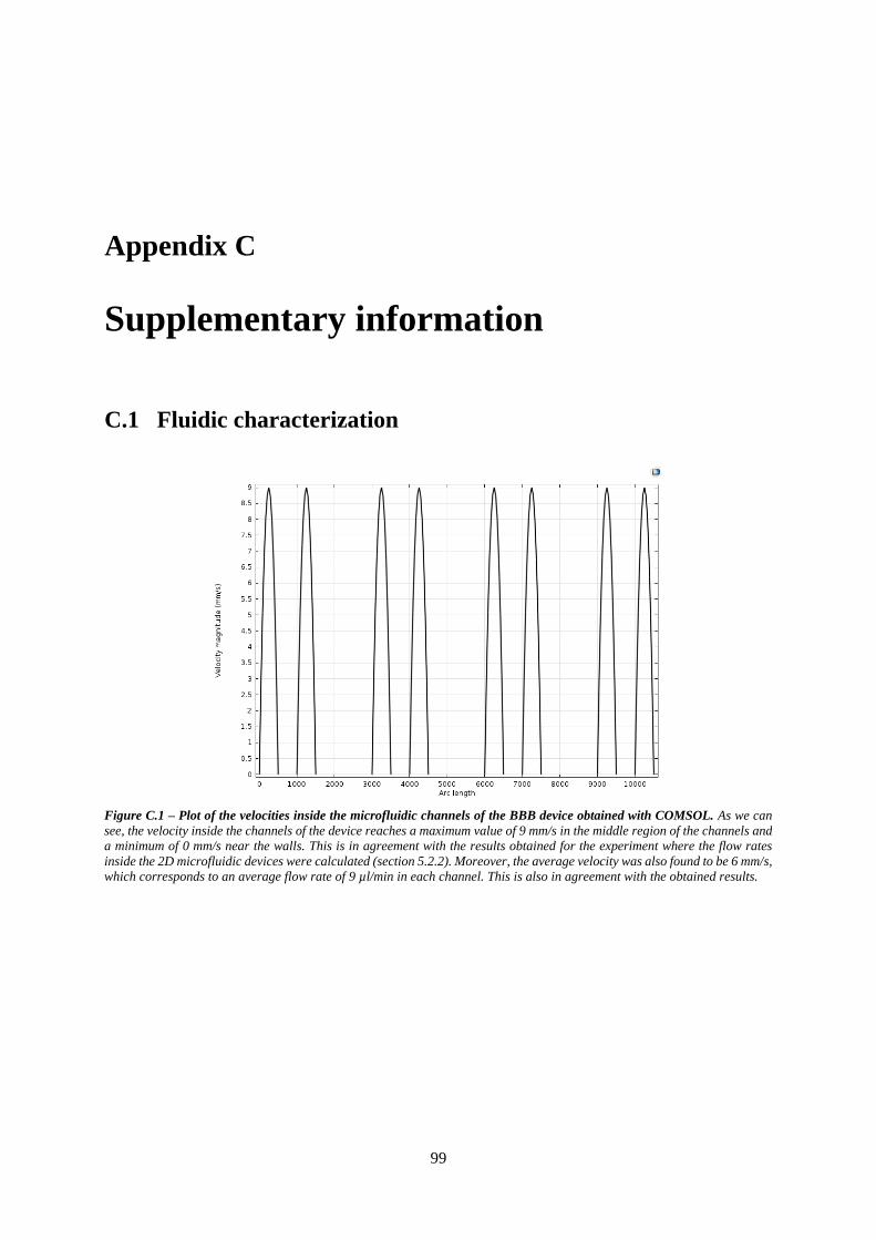
99
Appendix C
Supplementary information
C.1 Fluidic characterization
Figure C.1 – Plot of the velocities inside the microfluidic channels of the BBB device obtained with COMSOL. As we can
see, the velocity inside the channels of the device reaches a maximum value of 9 mm/s in the middle region of the channels and
a minimum of 0 mm/s near the walls. This is in agreement with the results obtained for the experiment where the flow rates
inside the 2D microfluidic devices were calculated (section 5.2.2). Moreover, the average velocity was also found to be 6 mm/s,
which corresponds to an average flow rate of 9 µl/min in each channel. This is also in agreement with the obtained results.
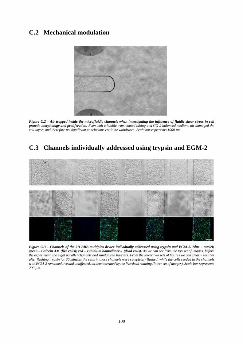
100
C.2 Mechanical modulation
C.3 Channels individually addressed using trypsin and EGM-2
Figure C.2 – Air trapped inside the microfluidic channels when investigating the influence of fluidic shear stress in cell
growth, morphology and proliferation. Even with a bubble trap, coated tubing and CO-2 balanced medium, air damaged the
cell layers and therefore no significant conclusions could be withdrawn. Scale bar represents 1000 µm.
Figure C.3 – Channels of the 2D BBB multiplex device individually addressed using trypsin and EGM-2. Blue – nuclei;
green – Calcein AM (live cells); red – Ethidium homodimer-1 (dead cells). As we can see from the top set of images, before
the experiment, the eight parallel channels had similar cell barriers. From the lower two sets of figures we can clearly see that
after flushing trypsin for 30 minutes the cells in those channels were completely flushed, while the cells seeded in the channels
with EGM-2 remained live and unaffected, as demonstrated by the live/dead staining (lower set of images). Scale bar represents
200 µm.

101
C.4 Dextran permeability assay
Channel
1 2 3 4 5 6 7 8
Pe
rme
ab
ility
co
effic
ients
(cm
/s)
0,000
0,001
0,002
0,003
0,004
C.5 TEER assay
Table C.1 - TEER values obtained for the cell layers seeded in device 1.
Chip 1
Channel Condition (Ω·cm2)
EGM-2 24 h. 48 h. 72 h. 96 h.
1 - 7.89 16.82 6.18 6.50
2 - 8.13 27.47 10.27 12.75
3 - 8.83 17.04 8.63 5.81
4 - 11.10 17.49 9.44 6.66
5 - 12.72 15.69 5.96 7.33
6 - 9.35 8.00 7.26 7.90
7 - 9.04 7.97 6.16 3.38
8 - 8.55 25.44 9.63 7.00
Average - 9.45 16.99 7.94 7.16
SD - 1.65 7.02 1.76 2.64
Figure C.4 – Permeability coefficients of the eight BBB’s of device 2 to the 40 kDa dextran. Only the coefficients obtained
for channels 4 and 7 could be calculated as there was not enough volume in the remaining collected samples. This was probably
caused by poor punching of the PC membrane when creating the connections between the bottom channels and their outlets.
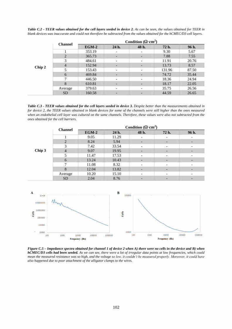
102
Table C.2 - TEER values obtained for the cell layers seeded in device 2. As can be seen, the values obtained for TEER in
blank devices was inaccurate and could not therefore be subtracted from the values obtained for the hCMEC/D3 cell layers.
Chip 2
Channel Condition (Ω·cm2)
EGM-2 24 h. 48 h. 72 h. 96 h.
1 353.19 - - 9.30 5.67
2 365.73 - - 7.88 7.55
3 484.61 - - 11.91 20.76
4 152.94 - - 13.73 8.57
5 153.43 - - 131.96 87.50
6 469.84 - - 74.72 35.44
7 446.50 - - 18.36 24.94
8 610.81 - - 18.17 22.05
Average 379.63 - - 35.75 26.56
SD 160.58 - - 44.59 26.65
Table C.3 - TEER values obtained for the cell layers seeded in device 3. Despite better than the measurements obtained in
for device 2, the TEER values obtained in blank devices for some of the channels were still higher than the ones measured
when an endothelial cell layer was cultured on the same channels. Therefore, these values were also not subtracted from the
ones obtained for the cell barriers.
Chip 3
Channel Condition (Ω·cm2)
EGM-2 24 h. 48 h. 72 h. 96 h.
1 9.05 11.29 - - -
2 8.24 5.94 - - -
3 7.42 33.54 - - -
4 9.07 19.95 - - -
5 11.47 17.53 - - -
6 13.24 10.43 - - -
7 11.08 8.32 - - -
8 12.04 13.82 - - -
Average 10.20 15.10 - - -
SD 2.04 8.76 - - -
Figure C.5 – Impedance spectra obtained for channel 1 of device 2 when A) there were no cells in the device and B) when
hCMEC/D3 cells had been seeded. As we can see, there were a lot of irregular data points at low frequencies, which could
mean the measured resistance was so high, and the voltage so low, it couldn’t be measured properly. Moreover, it could have
also happened due to poor attachment of the alligator clamps to the wires.
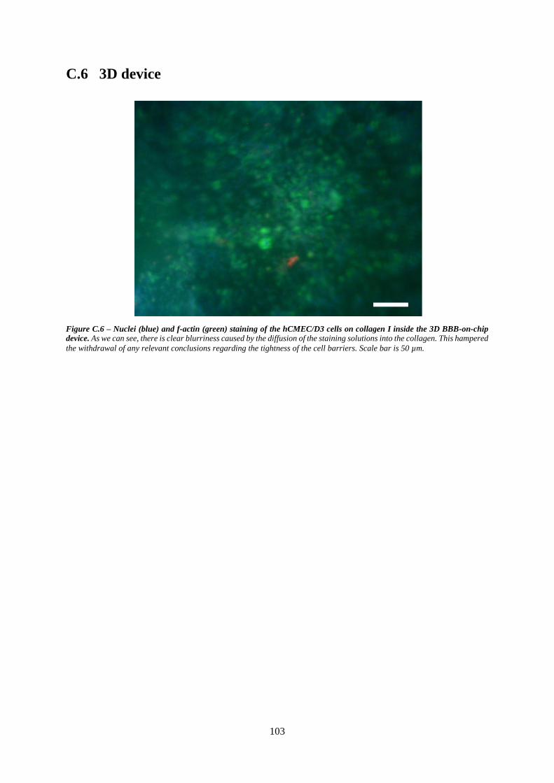
103
C.6 3D device
Figure C.6 – Nuclei (blue) and f-actin (green) staining of the hCMEC/D3 cells on collagen I inside the 3D BBB-on-chip
device. As we can see, there is clear blurriness caused by the diffusion of the staining solutions into the collagen. This hampered
the withdrawal of any relevant conclusions regarding the tightness of the cell barriers. Scale bar is 50 µm.

104
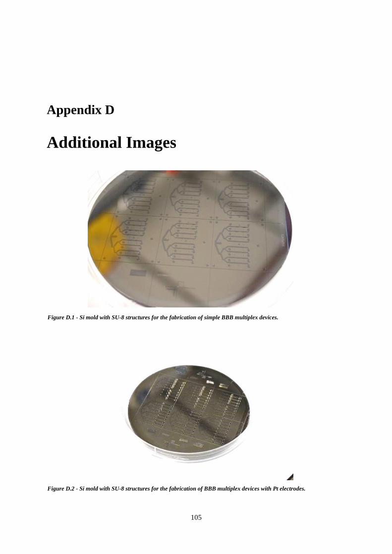
105
Appendix D
Additional Images
Figure D.1 - Si mold with SU-8 structures for the fabrication of simple BBB multiplex devices.
Figure D.2 - Si mold with SU-8 structures for the fabrication of BBB multiplex devices with Pt electrodes.
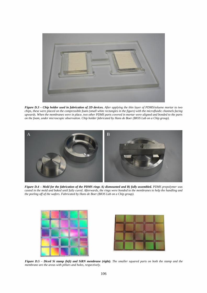
106
Figure D.3 – Chip holder used in fabrication of 2D devices. After applying the thin layer of PDMS/toluene mortar to two
chips, these were placed on the compressible foam (small white rectangles in the figure) with the microfluidic channels facing
upwards. When the membranes were in place, two other PDMS parts covered in mortar were aligned and bonded to the parts
on the foam, under microscopic observation. Chip holder fabricated by Hans de Boer (BIOS Lab on a Chip group).
Figure D.4 – Mold for the fabrication of the PDMS rings A) dismounted and B) fully assembled. PDMS prepolymer was
casted in the mold and baked until fully cured. Afterwards, the rings were bonded to the membranes to help the handling and
the peeling off of the wafers. Fabricated by Hans de Boer (BIOS Lab on a Chip group).
Figure D.5 – Diced Si stamp (left) and SiRN membrane (right). The smaller squared parts on both the stamp and the
membrane are the areas with pillars and holes, respectively.


![Microfluidic Organ‐on‐a‐Chip Technology for ...web.me.iastate.edu/hashemi/Caplin_Hashemi_Organ_Chip_Montaza… · [ 2 ] Organ-on-a-chip technology provides a practical solu-tion](https://img.pdfslide.us/doc/110x75/5f83c00f8cebff40bb7a548c/microfluidic-organaonaaachip-technology-for-webme-2-organ-on-a-chip.jpg)