Embed Size (px)
Citation preview

1 of 4
AbstractA 64-site wireless current microstimulator chip (Interestim-2B) and a prototype implant based on this chip have been developed for neural prosthesis applications. Modular stand-alone architecture allows up to 32 such chips to be connected in parallel to drive 2048 sites. The only off-chip components are a receiver inductive-capacitive (LC) tank and microelectrode arrays such as silicon probes for intracortical stimulation. The implant receives inductive power and data at 2.5 Mb/sec from a frequency shift keyed carrier to generate up to 65800 stimulus pulses/sec. Each chip contains 16 current drivers with 270 µA full-scale current, 5-bit resolution, 100 MΩ output impedance, and a dynamic range that extends within 150 mV of the 5 V supply rail. The chip and implant (without probes) measure 4.6×4.6×0.5 and 19×14×6 (mm), respectively.
Fig. 1. Block diagram of an Interestim-2B module [3].
Keywords Implant, microstimulator, modular, wireless
I. INTRODUCTION
Auditory function restoration in profoundly deaf individuals has been successfully achieved by implanting wireless stimulators capable of electrically stimulating the cochlea and auditory brain stem. Visual prostheses however, have not yet been widely utilized in the blind despite their longer history than some commercialized implantable devices such as deep brain stimulators [1]. The reason is the complexity of the visual system, which imposes severe technological challenges on an implant in terms of the number of stimulating sites, bandwidth, size,
power, and stimulation protocol. Several researchers have addressed the above problems with limited success [1], [2]. This paper presents Interestim-2B (IS-2B), a multichannel monolithic wireless microstimulator ASIC with a modular architecture, which advances the state-of-the-art in nearly all of the above directions. IS-2B can be assembled in a 64-module × 32-site wireless stimulating microsystem to address up to 2048 stimulating sites. Our ultimate goal is to develop button-sized wireless microstimulating 3D arrays by mounting IS-2B chips on micromachined platforms, connected to passive probes, or by implementing IS-2B circuitry on the backend of active silicon probes [3].
A Multichannel Monolithic Wireless Microstimulator
Khalil Najafi and Maysam Ghovanloo Center for Wireless Integrated Microsystems
Department of Electrical Engineering and Computer Science, University of Michigan, MI, USA
II. INTERESTIM-2B ARCHITECTURE
A. Interestim-2B Chip
Fig. 1 shows the block diagram of an IS-2B module [3]. There are two identical modules in each IS-2B chip, supporting a total of 64 stimulating sites. A hybrid receiver LC-tank circuit (LrCr), which can be shared between up to 32 chips via a pair of common inputs (C1, C2), provides each module with inductively attained power and data. Implant size reduction is achieved by utilizing a fully integrated full-wave CMOS rectifier [5] followed by an on-chip 430 pF capacitor. A 10 nF off-chip capacitor is used in parallel with the on-chip capacitor to achieve further ripple rejection. A regulator stabilizes VCC at 5 V for unregulated

2 of 4
inputs > 6.7 V, while supplying 1.65 mA to each module. In order to ensure safe operation, the power-on-reset (POR) circuit continuously monitors VCC and releases the reset line 70 µs after the regulator voltage > 4.8 V. It also shuts the entire stimulator down when VCC < 3.4 V.
The carrier frequency should be kept < 20 MHz due to the implanted coil self resonance and excessive power absorption in the tissue at higher frequencies. To achieve data rates comparable to the carrier frequency, FSK modulation scheme was utilized. Using a new FSK demodulator, data bits were detected by directly measuring the duration of each received carrier cycle [4]. The demodulator also derives a constant frequency clock from the FSK carrier. As a result, IS-2B is able to wirelessly receive 2.5 Mbps using an FSK carrier that switches between 5 and 10 MHz for logic 1 and 0, respectively.
Fig. 2. Current drivers schematic and block diagram [3], [6].
Isochronous communication scheme is adopted to provide a fast, steady, and uninterrupted data stream, which is preferred for video applications. The IS-2Bs 18-bit command frames, which consist of data and address bytes each accompanied by a parity bit, are transmitted back to back, separated by 1-bit spacers. An 18-bit shift register and a sequencer convert the serial bit-stream to parallel, while a pattern detector resets the sequencer upon receiving a unique frame (0FF0FFh) to maintain synchronization with the transmitter. The address byte consists of a 6-bit module-address and a 2-bit register-address. The module-address is compared to the modules hardwired user-programmable address, and if they match and there is no parity error, the data byte is stored in one of the four internal registers that is defined by the register-address. Otherwise, the received command frame is ignored.
Each module has eight current drivers (CD) that are enclosed in dashed boxes in Fig. 2. Each CD has both nMOS current sink (M1) and pMOS current source (M3) versions of a novel circuit topology that utilizes the above transistors in deep triode region as linearized voltage-controlled resistors (VCR) by applying a larger than
threshold VGS, while actively maintaining their VDS at 80 mV [6]. Linearity is achieved by using saturated auxiliary transistors in parallel with M1 and M3. The stimulus current amplitudes of all CDs are controlled by a dual pair of 5-bit voltage-mode DACs (DAC-n and DAC-p) with an additional bit for adjusting the offset current.
Each CDn, multiplexed among four stimulating sites, is controlled by two specific status-bits (An, Bn) and two shared mode-bits (MD0, MD1) as shown in Fig. 2. Combinations of these bits in four operating modes connect each site to VCC, current source, GND, current sink, common analog line (CAL), or keep it at high-Z. The result is a wide variety of stimulation strategies that can be applied depending on the application. CAL can be used for charge balancing, recording from sites, or site impedance measurement. There is also a reference line, controlled by FB0 and FB1 bits, which stays at high-Z in bipolar stimulation and can be connected to VCC, GND, or CAL for monopolar stimulation or impedance measurement [7].
B. Interestim-2B Implant
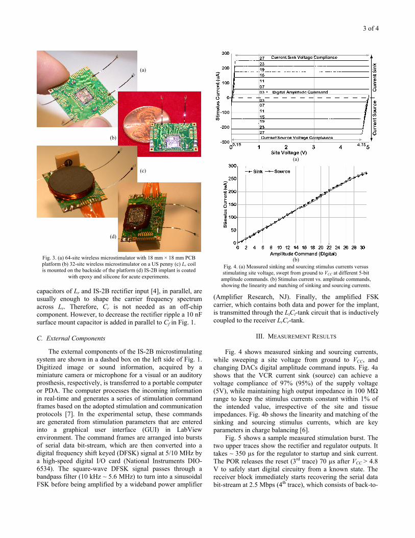
The IS-2B implant consists of the IS-2B wireless micro-stimulator ASIC, one or more stimulating microelectrode arrays, LrCr-tank, a platform, and packaging. Physical design of the package, platform, and stimulating probes highly depend on the application. Prototype IS-2B implants that are shown in Fig. 3 are designed for acute wireless intracortical microstimulation. Therefore, they were only coated with epoxy and silicone (Nusil Technology, CA) as a temporary package. Double layer, 0.4mm-thick printed circuit board (PCB) was used for the platform with 76.2µm minimum feature size. Two conservatively designed platforms, which include edge connectors for direct access to the sites as well as the ASIC test-points, are 18 mm × 18 mm and 18 mm × 13 mm in size and support two and four microelectrode arrays, respectively. The platform can be shrunk to 10 mm on each side by using a multilayer PCB and eliminating the edge connectors.
16-site micromachined silicon passive microelectrode arrays (called Rat-2) with 1cm flexible ribbon cables, which specifications are summarized in Table 1 [8], were glued to the platform with wax before being bonded. Unlike most other probes that have polysilicon interconnects running on their shanks and ribbon cable, these probes are equipped with metal (platinum) interconnects to minimize the access resistance to the stimulating sites. This is important in wireless microstimulators, where the implant supply voltage is limited and voltage dropout across the stimulating sites access lines can saturate the current drivers before achieving the desired stimulus current levels.
The receiver coil (Lr), which specifications are shown in Table 1, is wound around a ferrite core (Fair-Rite, NY) to intensify the electromagnetic field and increase the coupling with an external transmitter coil (Lt). Lr is attached to the backside of the platform using double-sticky tape. Parasitic
3 of 4
(a)
Fig. 3. (a) 64-site wireless microstimulator with 18 mm × 18 mm PCB platform (b) 32-site wireless microstimulator on a US penny (c) Lr coil is mounted on the backside of the platform (d) IS-2B implant is coated
with epoxy and silicone for acute experiments.
(b)
(a)
(c)
(d)
(b) Fig. 4. (a) Measured sinking and sourcing stimulus currents versus stimulating site voltage, swept from ground to VCC at different 5-bit
amplitude commands. (b) Stimulus current vs. amplitude commands, showing the linearity and matching of sinking and sourcing currents.
capacitors of Lr and IS-2B rectifier input [4], in parallel, are usually enough to shape the carrier frequency spectrum across Lr. Therefore, Cr is not needed as an off-chip component. However, to decrease the rectifier ripple a 10 nF surface mount capacitor is added in parallel to Cf in Fig. 1.
C. External Components
The external components of the IS-2B microstimulating system are shown in a dashed box on the left side of Fig. 1. Digitized image or sound information, acquired by a miniature camera or microphone for a visual or an auditory prosthesis, respectively, is transferred to a portable computer or PDA. The computer processes the incoming information in real-time and generates a series of stimulation command frames based on the adopted stimulation and communication protocols [7]. In the experimental setup, these commands are generated from stimulation parameters that are entered into a graphical user interface (GUI) in LabView environment. The command frames are arranged into bursts of serial data bit-stream, which are then converted into a digital frequency shift keyed (DFSK) signal at 5/10 MHz by a high-speed digital I/O card (National Instruments DIO-6534). The square-wave DFSK signal passes through a bandpass filter (10 kHz ~ 5.6 MHz) to turn into a sinusoidal FSK before being amplified by a wideband power amplifier
(Amplifier Research, NJ). Finally, the amplified FSK carrier, which contains both data and power for the implant, is transmitted through the LtCt-tank circuit that is inductively coupled to the receiver LrCr-tank.
III. MEASUREMENT RESULTS
Fig. 4 shows measured sinking and sourcing currents, while sweeping a site voltage from ground to VCC, and changing DACs digital amplitude command inputs. Fig. 4a shows that the VCR current sink (source) can achieve a voltage compliance of 97% (95%) of the supply voltage (5V), while maintaining high output impedance in 100 MΩ range to keep the stimulus currents constant within 1% of the intended value, irrespective of the site and tissue impedances. Fig. 4b shows the linearity and matching of the sinking and sourcing stimulus currents, which are key parameters in charge balancing [6].
Fig. 5 shows a sample measured stimulation burst. The two upper traces show the rectifier and regulator outputs. It takes ~ 350 µs for the regulator to startup and sink current. The POR releases the reset (3rd trace) 70 µs after VCC > 4.8 V to safely start digital circuitry from a known state. The receiver block immediately starts recovering the serial data bit-stream at 2.5 Mbps (4th trace), which consists of back-to-

4 of 4
TABLE 1 INTERESTIM-2B SPECIFICATIONS
IS-2B ASIC Process technology AMI 1.5-µm CMOS
Die size 4.6 × 4.6 × 0.5 (mm)
Module per chip 2 Current drivers per module 8
Stimulating sites per module 32
Max number of addressable modules 64
Total number of addressable sites 2048 Power and data source Inductive coupling
Power consumption per module 8.25 mW @ 5 V Number of transistors per module 6500
Telemetry Communication scheme Isochronous
Modulation scheme FSK Carrier frequency 5/10 MHz
Command frame size 18-bits + 1-spacer Data rate / Bit error rate (BER) 2.5 Mbps / 10 ppm
Nominal coupling distance 5 mm Receiver Coil Size ∅13 × 3 (mm)
Number of turns / Lr 15 / 9 µH Stimulation
Supported stimulation protocols 8 Full-scale stimulation current 270 µA
Stimulation amplitude resolution 8.43 µA (5-bits)
Current source/sink compliance voltage 4.75 V / 4.85 V Current driver output impedance ~ 100 MΩ
Timing resolution / accuracy 7.6 µs / 50 ns Max stimulation pulse rate 65800 pulses/sec
Silicon Microelectrode Array (Rat-2) Number of stimulating sites / Array 16 / 4 × 4
Site coating Iridium Oxide Average site impedance before/after activation 210 kΩ / 45 kΩ
Site area / Spacing ~ 1000 µm2 / 250 µm Shank size 1500 × 80 × 15 (µm)
Ribbon cable size 10 mm × 250 µm IS-2B Implant
Backend size (without probes) 19 × 14 × 6 (mm)
Fig. 5. Wireless operation of the IS-2B microstimulating system. From top: CMOS rectifier output, regulator output, POR output,
demodulated data bit-stream, Site0 single-ended voltage, differential voltage across a 10 kΩ resistor between Site0 and Site4, Site4 voltage
back command frames. The stimulation burst, shown on the three lower traces, starts as soon as the digital block synchronizes with the transmitter by detecting the unique frame that is sent between every 2 stimulation pulses in this specific example. A 10 kΩ load, resembling sites and tissue impedances, is connected between Site0 and Site4. Single-ended voltages at these sites and their subtraction are shown in Fig. 5 three lower traces, which are also magnified in Fig. 5 inset. Three initialization commands set the sourcing and sinking stimulus amplitudes to full-scale and connect CD0 and CD1 outputs to Site0 and Site4 (see Fig. 2). The 1st stimulation command connects Site4 (Site0) to a source (sink). As a result, 270 µA flows from Site4 to Site0 in the cathodic phase. The 2nd command puts both sites in the high-Z state for an interphase delay. The 3rd command swaps the sites status and 270 µA flows back from Site0 to Site4 in the anodic phase. Finally, the 4th command returns both sites to high-Z. The duration of every command, including the spacer bit, is 7.6 µs. Therefore, considering that at least two commands are needed per stimulation phase, IS-2B can generate up to 65800 pulses per second.
REFERENCES [1] R.A. Normann, Sight restoration for individuals with profound
blindness, Available: http://www.bioen.utah.edu/cni/projects [2] W. Liu et al., A neuro-stimulus chip with telemetry unit for retinal
prosthetic device, IEEE J. Solid-State Circuits, vol. 35, no. 10, pp. 1487-1497, Oct. 2001.
[3] M. Ghovanloo and K. Najafi, A modular 32-site wireless neural stimulation microsystem, IEEE Solid-State Circuits Conference, Digest of technical papers, pp. 226-227, Feb. 2004.
IV. CONCLUSION [4] , Fully integrated wideband high-current rectifiers for inductively powered biomedical implants, IEEE Journal on Solid-State Circuits, accepted for publication.
A multichannel monolithic wireless microstimulating system (Interestim-2B) is developed for neural prosthesis applications by integrating all the required circuitry on an ASIC except for the receiver LC-tank. Each IS-2B chip drives 64 stimulating sites, and its modular stand-alone architecture makes it possible to address up to 32 chips in parallel to drive 2048 sites. Table 1 summarizes the specs of a prototype implant based on IS-2B for acute intracortical stimulation. Experimental in vitro and in vivo results with IS-2B microsystem are discussed in [7].
[5] , A fully digital frequency shift keying demodulator chip for the wireless biomedical implants, Proc. IEEE Southwest Symp. Mixed-Signal Design, pp. 223-227, Feb. 2003.
[6] , A small size large voltage compliance programmable current source for biomedical implantable microstimulators, Proc. IEEE 25th EMBS Conf., pp. 1979-1982, Sep. 2003.
[7] M. Ghovanloo, K.J. Otto, D.R. Kipke, and K. Najafi, In Vitro and In Vivo Testing of a Wireless Multichannel Stimulating Telemetry Microsystem, Unpublished.
[8] Center for Neural Communication Technology (CNCT), Available: http://www.engin.umich.edu/center/cnct/